CN108447987B - Preparation method of low-activation-voltage resistance change device - Google Patents
Preparation method of low-activation-voltage resistance change deviceDownload PDFInfo
- Publication number
- CN108447987B CN108447987BCN201810396055.7ACN201810396055ACN108447987BCN 108447987 BCN108447987 BCN 108447987BCN 201810396055 ACN201810396055 ACN 201810396055ACN 108447987 BCN108447987 BCN 108447987B
- Authority
- CN
- China
- Prior art keywords
- dielectric layer
- preparation
- low
- precursor solution
- activation
- Prior art date
- Legal status (The legal status is an assumption and is not a legal conclusion. Google has not performed a legal analysis and makes no representation as to the accuracy of the status listed.)
- Expired - Fee Related
Links
Images


Classifications
- H—ELECTRICITY
- H10—SEMICONDUCTOR DEVICES; ELECTRIC SOLID-STATE DEVICES NOT OTHERWISE PROVIDED FOR
- H10N—ELECTRIC SOLID-STATE DEVICES NOT OTHERWISE PROVIDED FOR
- H10N70/00—Solid-state devices having no potential barriers, and specially adapted for rectifying, amplifying, oscillating or switching
- H10N70/20—Multistable switching devices, e.g. memristors
- H10N70/24—Multistable switching devices, e.g. memristors based on migration or redistribution of ionic species, e.g. anions, vacancies
- H—ELECTRICITY
- H10—SEMICONDUCTOR DEVICES; ELECTRIC SOLID-STATE DEVICES NOT OTHERWISE PROVIDED FOR
- H10N—ELECTRIC SOLID-STATE DEVICES NOT OTHERWISE PROVIDED FOR
- H10N70/00—Solid-state devices having no potential barriers, and specially adapted for rectifying, amplifying, oscillating or switching
- H10N70/011—Manufacture or treatment of multistable switching devices
- H10N70/021—Formation of switching materials, e.g. deposition of layers
- H—ELECTRICITY
- H10—SEMICONDUCTOR DEVICES; ELECTRIC SOLID-STATE DEVICES NOT OTHERWISE PROVIDED FOR
- H10N—ELECTRIC SOLID-STATE DEVICES NOT OTHERWISE PROVIDED FOR
- H10N70/00—Solid-state devices having no potential barriers, and specially adapted for rectifying, amplifying, oscillating or switching
- H10N70/011—Manufacture or treatment of multistable switching devices
- H10N70/041—Modification of switching materials after formation, e.g. doping
Landscapes
- Engineering & Computer Science (AREA)
- Manufacturing & Machinery (AREA)
- Semiconductor Memories (AREA)
Abstract
Translated fromChinese
Description
Translated fromChinese技术领域technical field
本发明涉及信息存储的技术领域,更具体地,涉及一种低激活电压阻变器件的制备方法。The present invention relates to the technical field of information storage, and more particularly, to a preparation method of a low activation voltage resistive switching device.
背景技术Background technique
随着手机、平板电脑等一系列产品在我们的生活中越来越普及,便携式电子产品受到越来越多的关注,相应的市场也空前巨大。其中,存储器作为电子产品的核心部件对器件的性能有着十分重要的作用。然而,受限于晶体管集成技术,以及尺寸微小化的瓶颈,当前市场的主流产品闪存(Flash)已无法满足市场及半导体产业对存储器的需求。因此,近年来国内外广大科研人员针对下一代存储器开展了许多研究。As a series of products such as mobile phones and tablet computers become more and more popular in our lives, portable electronic products receive more and more attention, and the corresponding market is unprecedentedly huge. Among them, the memory, as the core component of electronic products, plays a very important role in the performance of the device. However, limited by transistor integration technology and the bottleneck of size miniaturization, the current mainstream product Flash (Flash) in the market has been unable to meet the needs of the market and the semiconductor industry for memory. Therefore, in recent years, researchers at home and abroad have carried out a lot of research on the next-generation memory.
阻变存储器,因具有断电保持能力、快速读写、高存储密度、低功耗且结构简单易于制备等优势,被认为是下一代存储器的最有力的竞争者之一。但是,阻变存储器往往需要一个很高的激活电压,来刺激介质层使缺陷(如氧空位)在局部产生聚集,进而才能实现状态的切换。这一问题的存在严重制约了阻变存储器的应用。因此,想要有效降低激活电压甚至消除激活过程,就必须对阻变介质层中的缺陷形成能进行有效调控。研究中发现,缺陷形成能较低的介质层材料其阻变存储特性往往不理想,甚至不具备阻变特性。而存储特性较好的介质层材料,其缺陷形成能往往较高。Resistive memory is considered to be one of the most powerful competitors for next-generation memory due to its advantages of power-off retention capability, fast read and write, high storage density, low power consumption, and simple structure and easy preparation. However, resistive memory often requires a very high activation voltage to stimulate the dielectric layer to cause defects (such as oxygen vacancies) to locally aggregate, so as to achieve state switching. The existence of this problem seriously restricts the application of resistive memory. Therefore, in order to effectively reduce the activation voltage or even eliminate the activation process, it is necessary to effectively control the defect formation energy in the resistive dielectric layer. It is found in the research that the resistive memory properties of dielectric layer materials with low defect formation energy are often unsatisfactory, or even do not have resistive switching properties. However, the dielectric layer materials with better storage properties tend to have higher defect formation energies.
因此,如何调控阻变介质层中的缺陷形成能就成了关键。目前,阻变介质层的主要制备方法是溅射法。通过掺杂的靶材沉积,或是在电极与介质层之间形成过渡层来增加氧空位的含量,从而在一定程度上减小激活电压。但是介质层在制备时其成分的控制要求比较精确,对实验设备、工艺参数有很高的要求。此外,过渡层的化学计量比、厚度等条件需要严格控制,其对应的电极材料也有特殊的要求。Therefore, how to control the defect formation energy in the resistive dielectric layer becomes the key. At present, the main preparation method of the resistive dielectric layer is sputtering. The content of oxygen vacancies is increased by doped target deposition or by forming a transition layer between the electrode and the dielectric layer, thereby reducing the activation voltage to a certain extent. However, the control of the composition of the dielectric layer is relatively precise during the preparation, and it has high requirements for experimental equipment and process parameters. In addition, the stoichiometric ratio, thickness and other conditions of the transition layer need to be strictly controlled, and the corresponding electrode materials also have special requirements.
发明内容SUMMARY OF THE INVENTION
本发明为克服上述现有技术所述的至少一种缺陷,提供一种低激活电压阻变器件的制备方法,提出一种控制难度小、成本低廉、对设备要求低、可行性高的方法来有效调控阻变介质层中的缺陷形成能,从而大幅降低阻变器件的激活电压,消除激活过程的不利影响。In order to overcome at least one of the above-mentioned defects in the prior art, the present invention provides a preparation method of a low activation voltage resistive device, and proposes a method with low control difficulty, low cost, low equipment requirements and high feasibility. The defect formation energy in the resistive switching medium layer is effectively regulated, thereby greatly reducing the activation voltage of the resistive switching device and eliminating the adverse effects of the activation process.
本发明的技术方案是:一种低激活电压阻变器件的制备方法,包括以下步骤:The technical scheme of the present invention is: a preparation method of a low activation voltage resistive device, comprising the following steps:
步骤1)、对导电衬底进行表面清洗和预处理后待用;Step 1), carry out surface cleaning and pretreatment to the conductive substrate for later use;
步骤2)、随后,在导电衬底上生长并热处理后得到介质层S1;Step 2), subsequently, growing on the conductive substrate and heat-treating to obtain a dielectric layer S1;
步骤3)、配制介质层S2的前驱体溶液A2,并加入腐蚀剂得到混合前驱体溶液A3;Step 3), preparing a precursor solution A2 of the dielectric layer S2, and adding an etchant to obtain a mixed precursor solution A3;
步骤4)、将混合前驱体溶液A3旋涂在介质层S1上并热处理得到复合介质层S2(1)/S1;Step 4), spin-coating the mixed precursor solution A3 on the dielectric layer S1 and heat treatment to obtain a composite dielectric layer S2(1)/S1;
步骤5)、在复合介质层S2(1)/S1上蒸镀顶电极,完成制备。Step 5): Evaporating a top electrode on the composite dielectric layer S2(1)/S1 to complete the preparation.
进一步的,所述的步骤2)中所述介质层S1为ITO、IZO、In2O3、InOx中的一种或几种。Further, in the step 2), the medium layer S1 is one or more of ITO, IZO, In2 O3 , and InOx .
所述的步骤2)中所述热处理的温度为100-300 ℃。The temperature of the heat treatment in the step 2) is 100-300°C.
所述的步骤3)中所述介质层S2为Al2O3。In the step 3), the dielectric layer S2 is Al2 O3 .
所述的步骤3)中所述前驱体溶液A2中,溶剂为H2O2。In the precursor solution A2 in the step 3), the solvent is H2 O2 .
所述的步骤3)中所述前驱体溶液A2的浓度为0.05 mol/L-0.3 mol/L。In the step 3), the concentration of the precursor solution A2 is 0.05 mol/L-0.3 mol/L.
所述的步骤3)中所述腐蚀剂为NH3·H2O和HNO3。In the step 3), the etchants are NH3 ·H2 O and HNO3 .
所述的步骤4)中所述热处理的温度为100-200 ℃。The temperature of the heat treatment in the step 4) is 100-200°C.
所述的步骤4)中所述介质层S2(1)的厚度为10-40 nm。In the step 4), the thickness of the dielectric layer S2(1) is 10-40 nm.
所述的步骤4)中所述介质层S2(1),为介质层S2与部分介质层S1形成的混合层;步骤5)中所述顶电极为Au、Ag、Ni、Al、Pt中的一种或几种。The dielectric layer S2(1) in the step 4) is a mixed layer formed by the dielectric layer S2 and part of the dielectric layer S1; the top electrode in the step 5) is Au, Ag, Ni, Al, and Pt. one or more.
与现有技术相比,有益效果是:本发明通过在高形成能介质层的前驱体中添加腐蚀剂,在高形成能介质层的成型过程中对低形成能的介质层表面进行适当腐蚀,从而形成同时具有阻变特性和低形成能的混合介质层。在高形成能介质层的成型过程中对低形成能介质层表面进行腐蚀,可以使混合更加充分,避免纯相的高形成能介质层产生。本发明具有操作简单、对设备要求低、易于重复试验、性能优异等优点,可作为调控介质层缺陷形成能、大幅降低激活电压的理想方法。经反复实验表明,本发明的有益效果将会在下面的描述中更加明显。Compared with the prior art, the beneficial effect is as follows: the present invention appropriately etches the surface of the low-forming-energy dielectric layer during the molding process of the high-forming-energy dielectric layer by adding an etchant to the precursor of the high-forming-energy dielectric layer, thereby A mixed dielectric layer with both resistive switching properties and low formation energy is formed. Etching the surface of the low-forming-energy medium layer during the forming process of the high-forming-energy medium layer can make mixing more sufficient and avoid the generation of a pure-phase high-forming-energy medium layer. The invention has the advantages of simple operation, low requirements for equipment, easy repeated test, excellent performance and the like, and can be used as an ideal method for regulating the defect formation energy of the dielectric layer and greatly reducing the activation voltage. Repeated experiments show that the beneficial effects of the present invention will be more apparent in the following description.
附图说明Description of drawings
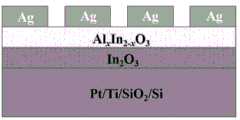
图1为实施例1制备得到的阻变单元的结构示意图。FIG. 1 is a schematic structural diagram of the resistive switching unit prepared in Example 1. FIG.
图2为实施例1中阻变单元的电流-电压曲线。FIG. 2 is a current-voltage curve of the resistive switching unit in Example 1. FIG.
图3为对比例1制备得到的阻变单元的结构示意图。FIG. 3 is a schematic structural diagram of the resistive switching unit prepared in Comparative Example 1. FIG.
图4为对比例1中阻变单元的电流-电压曲线。FIG. 4 is a current-voltage curve of the resistive switching unit in Comparative Example 1. FIG.
图5为对比例2制备得到的阻变单元的结构示意图。FIG. 5 is a schematic structural diagram of the resistive switching unit prepared in Comparative Example 2. FIG.
图6为对比例2中阻变单元的电流-电压曲线。FIG. 6 is a current-voltage curve of the resistive switching unit in Comparative Example 2. FIG.
具体实施方式Detailed ways
附图仅用于示例性说明,不能理解为对本专利的限制;为了更好说明本实施例,附图某些部件会有省略、放大或缩小,并不代表实际产品的尺寸;对于本领域技术人员来说,附图中某些公知结构及其说明可能省略是可以理解的。附图中描述位置关系仅用于示例性说明,不能理解为对本专利的限制。The accompanying drawings are for illustrative purposes only, and should not be construed as limitations on this patent; in order to better illustrate the present embodiment, some parts of the accompanying drawings may be omitted, enlarged or reduced, and do not represent the size of the actual product; for those skilled in the art It is understandable to the artisan that certain well-known structures and descriptions thereof may be omitted from the drawings. The positional relationships described in the drawings are only for exemplary illustration, and should not be construed as a limitation on the present patent.
实施例1Example 1
将长1 cm,宽1 cm的Pt/Ti/SiO2/Si衬底分别用丙酮、异丙醇、去离子水清洗,烘干后备用。The Pt/Ti/SiO2 /Si substrate with a length of 1 cm and a width of 1 cm was washed with acetone, isopropanol, and deionized water, respectively, and dried for later use.
配置0.2 mol/L的硝酸铟水溶液并搅拌24 h后待用。A 0.2 mol/L indium nitrate aqueous solution was prepared and stirred for 24 h before use.
称取一定量固体硝酸铝溶解于2.5 ml 双氧水(30%)中,配置成0.2 mol/L的硝酸铝溶液。A certain amount of solid aluminum nitrate was weighed and dissolved in 2.5 ml of hydrogen peroxide (30%) to prepare a 0.2 mol/L aluminum nitrate solution.
向硝酸铝溶液中加入111 μL氨水和75 μL硝酸,并搅拌24 h得到硝酸铝混合溶液。111 μL of ammonia water and 75 μL of nitric acid were added to the aluminum nitrate solution, and stirred for 24 h to obtain a mixed solution of aluminum nitrate.
将硝酸铟水溶液旋涂在Pt/Ti/SiO2/Si衬底上,之后置于加热板上加热5 min。该过程重复操作4次。随后将样品至于退火炉中180 ℃退火1 h,之后让样品自然冷却至室温。The aqueous solution of indium nitrate was spin-coated on the Pt/Ti/SiO2 /Si substrate, and then placed on a heating plate for 5 min. This process is repeated 4 times. The samples were then annealed in an annealing furnace at 180 °C for 1 h, and then allowed to cool to room temperature naturally.
样品取出后,将硝酸铝混合溶液在样品上旋涂,之后置于退火炉中180 ℃退火30min。该过程重复操作2次。之后让样品自然冷却至室温。After the sample was taken out, the mixed solution of aluminum nitrate was spin-coated on the sample, and then placed in an annealing furnace for annealing at 180 °C for 30 min. This process is repeated 2 times. The samples were then allowed to cool to room temperature naturally.
样品取出后用孔径100 μm的掩膜板遮盖,再置于电子束蒸发镀膜机中生长上电极,溅射靶材为99.99%的Ag,生长厚度为140 nm。After the sample was taken out, it was covered with a mask plate with an aperture of 100 μm, and then placed in an electron beam evaporation coating machine to grow the upper electrode. The sputtering target was 99.99% Ag, and the growth thickness was 140 nm.
完成上述步骤后取出样品,制备完毕。After completing the above steps, take out the sample, and the preparation is complete.
经过透射电镜截面与能谱分析,介质层结构为AlxIn2-xO3(20 nm)/In2O3(30 nm),单元结构为Ag/AlxIn2-xO3/In2O3/Pt/Ti/SiO2/Si。正常情况下,所制备的介质层结构应当为Al2O3/In2O3。但是由于Al2O3的前驱体溶液中添加有硝酸,热处理过程中会腐蚀In2O3的上表面,使部分In2O3溶解混入到Al2O3的前驱体溶液中。因此,在对Al2O3的前驱体溶液进行热处理后会形成AlxIn2-xO3混合介质层。其中,In2O3是一种氧空位形成能较低(<2 eV)的介质层,而Al2O3是一种氧空位形成能较高(>6 eV)的介质层。采用半导体分析仪对单元的电学特性进行表征。由图2可以看出,当操作电压仅为0.27 V时,单元中电流发生突变,实现状态切换。Through TEM cross-section and energy spectrum analysis, the structure of the dielectric layer is Alx In2-x O3 (20 nm)/In2 O3 (30 nm), and the unit structure is Ag/Alx In2-x O3 /In2 O3 /Pt/Ti/SiO2 /Si. Normally, the prepared dielectric layer structure should be Al2 O3 /In2 O3 . However, due to the addition of nitric acid to the Al2 O3 precursor solution, the upper surface of In2 O3 will be corroded during the heat treatment process, so that part of In2 O3 is dissolved and mixed into the Al2 O3 precursor solution. Therefore, anAlxIn2-xO3 mixed dielectric layer is formed after heat treatmentof theAl2O3 precursor solution. Among them, In2 O3 is a dielectric layer with low oxygen vacancy formation energy (<2 eV), while Al2 O3 is a dielectric layer with high oxygen vacancy formation energy (>6 eV). The electrical properties of the cells were characterized using a semiconductor analyzer. It can be seen from Figure 2 that when the operating voltage is only 0.27 V, the current in the cell changes abruptly to achieve state switching.
实施例2Example 2
将长1 cm,宽1 cm的Pt/Ti/SiO2/Si衬底分别用丙酮、异丙醇、去离子水清洗,烘干后备用。The Pt/Ti/SiO2 /Si substrate with a length of 1 cm and a width of 1 cm was washed with acetone, isopropanol, and deionized water, respectively, and dried for later use.
配置0.22 mol/L的硝酸铟水溶液并搅拌24 h后待用。A 0.22 mol/L indium nitrate aqueous solution was prepared and stirred for 24 h before use.
称取一定量固体硝酸铝溶解于2.5 ml 双氧水(30%)中,配置成0.18 mol/L的硝酸铝溶液。A certain amount of solid aluminum nitrate was weighed and dissolved in 2.5 ml of hydrogen peroxide (30%) to prepare a 0.18 mol/L aluminum nitrate solution.
向硝酸铝溶液中加入111 μL氨水和75 μL硝酸,并搅拌24 h得到硝酸铝混合溶液。111 μL of ammonia water and 75 μL of nitric acid were added to the aluminum nitrate solution, and stirred for 24 h to obtain a mixed solution of aluminum nitrate.
将硝酸铟水溶液旋涂在Pt/Ti/SiO2/Si衬底上,之后置于加热板上加热5 min。该过程重复操作4次。随后将样品至于退火炉中150 ℃退火1 h,之后让样品自然冷却至室温。The aqueous solution of indium nitrate was spin-coated on the Pt/Ti/SiO2 /Si substrate, and then placed on a heating plate for 5 min. This process is repeated 4 times. The samples were then annealed in an annealing furnace at 150 °C for 1 h, and then allowed to cool to room temperature naturally.
样品取出后,将硝酸铝混合溶液在样品上旋涂,之后置于退火炉中150 ℃退火30min。该过程重复操作3次。之后让样品自然冷却至室温。After the sample was taken out, the mixed solution of aluminum nitrate was spin-coated on the sample, and then placed in an annealing furnace for annealing at 150 °C for 30 min. This process is repeated 3 times. The samples were then allowed to cool to room temperature naturally.
样品取出后用孔径100 μm的掩膜板遮盖,再置于电子束蒸发镀膜机中生长上电极,溅射靶材为99.99%的Ag,生长厚度为140 nm。After the sample was taken out, it was covered with a mask plate with an aperture of 100 μm, and then placed in an electron beam evaporation coating machine to grow the upper electrode. The sputtering target was 99.99% Ag, and the growth thickness was 140 nm.
完成上述步骤后取出样品,制备完毕。After completing the above steps, take out the sample, and the preparation is complete.
实施例3Example 3
将长1 cm,宽1 cm的Pt/Ti/SiO2/Si衬底分别用丙酮、异丙醇、去离子水清洗,烘干后备用。The Pt/Ti/SiO2 /Si substrate with a length of 1 cm and a width of 1 cm was washed with acetone, isopropanol, and deionized water, respectively, and dried for later use.
配置0.22 mol/L的硝酸铟水溶液并搅拌24 h后待用。A 0.22 mol/L indium nitrate aqueous solution was prepared and stirred for 24 h before use.
称取一定量固体硝酸铝溶解于2.5 ml 双氧水(30%)中,配置成0.2 mol/L的硝酸铝溶液。A certain amount of solid aluminum nitrate was weighed and dissolved in 2.5 ml of hydrogen peroxide (30%) to prepare a 0.2 mol/L aluminum nitrate solution.
向硝酸铝溶液中加入111 μL氨水和75 μL硝酸,并搅拌24 h得到硝酸铝混合溶液。111 μL of ammonia water and 75 μL of nitric acid were added to the aluminum nitrate solution, and stirred for 24 h to obtain a mixed solution of aluminum nitrate.
将硝酸铟水溶液旋涂在Pt/Ti/SiO2/Si衬底上,之后置于加热板上加热5 min。该过程重复操作4次。随后将样品至于退火炉中180 ℃退火1 h,之后让样品自然冷却至室温。The aqueous solution of indium nitrate was spin-coated on the Pt/Ti/SiO2 /Si substrate, and then placed on a heating plate for 5 min. This process is repeated 4 times. The samples were then annealed in an annealing furnace at 180 °C for 1 h, and then allowed to cool to room temperature naturally.
样品取出后,将硝酸铝混合溶液在样品上旋涂,之后置于退火炉中150 ℃退火30min。该过程重复操作2次。之后让样品自然冷却至室温。After the sample was taken out, the mixed solution of aluminum nitrate was spin-coated on the sample, and then placed in an annealing furnace for annealing at 150 °C for 30 min. This process is repeated 2 times. The samples were then allowed to cool to room temperature naturally.
样品取出后用孔径100 μm的掩膜板遮盖,再置于电子束蒸发镀膜机中生长上电极,溅射靶材为99.99%的Au,生长厚度为140 nm。After the sample was taken out, it was covered with a mask plate with an aperture of 100 μm, and then placed in an electron beam evaporation coating machine to grow the upper electrode. The sputtering target was 99.99% Au, and the growth thickness was 140 nm.
完成上述步骤后取出样品,制备完毕。After completing the above steps, take out the sample, and the preparation is complete.
对比例1Comparative Example 1
为了说明经腐蚀产生的混合层的作用,制备了Ag/Al2O3/Pt/Ti/SiO2/Si单元,除了未制备In2O3层外,其余和实施例1一致。In order to illustrate the effect of the mixed layer produced by etching, Ag/Al2 O3 /Pt/Ti/SiO2 /Si units were prepared, which were the same as in Example 1 except that the In2 O3 layer was not prepared.
由图4可以看出,单元需要较高的激活电压,达到了1.82 V,显著高于实施例1。It can be seen from FIG. 4 that the cell requires a higher activation voltage, reaching 1.82 V, which is significantly higher than that of Example 1.
对比例2Comparative Example 2
为了说明经腐蚀产生的混合层的作用,制备了Ag/In2O3/Pt/Ti/SiO2/Si单元,除了未制备Al2O3层外,其余和实施例1一致。In order to illustrate the effect of the mixed layer produced by etching, Ag/In2 O3 /Pt/Ti/SiO2 /Si units were prepared, which were the same as in Example 1 except that the Al2 O3 layer was not prepared.
由图6可以看出,单元始终处于高电流状态,无法实现状态切换。即单元不具备阻变特性。It can be seen from Figure 6 that the unit is always in a high current state and cannot achieve state switching. That is, the unit does not have resistive characteristics.
显然,本发明的上述实施例仅仅是为清楚地说明本发明所作的举例,而并非是对本发明的实施方式的限定。对于所属领域的普通技术人员来说,在上述说明的基础上还可以做出其它不同形式的变化或变动。这里无需也无法对所有的实施方式予以穷举。凡在本发明的精神和原则之内所作的任何修改、等同替换和改进等,均应包含在本发明权利要求的保护范围之内。Obviously, the above-mentioned embodiments of the present invention are only examples for clearly illustrating the present invention, rather than limiting the embodiments of the present invention. For those of ordinary skill in the art, changes or modifications in other different forms can also be made on the basis of the above description. There is no need and cannot be exhaustive of all implementations here. Any modifications, equivalent replacements and improvements made within the spirit and principle of the present invention shall be included within the protection scope of the claims of the present invention.
Claims (7)
Priority Applications (1)
| Application Number | Priority Date | Filing Date | Title |
|---|---|---|---|
| CN201810396055.7ACN108447987B (en) | 2018-04-27 | 2018-04-27 | Preparation method of low-activation-voltage resistance change device |
Applications Claiming Priority (1)
| Application Number | Priority Date | Filing Date | Title |
|---|---|---|---|
| CN201810396055.7ACN108447987B (en) | 2018-04-27 | 2018-04-27 | Preparation method of low-activation-voltage resistance change device |
Publications (2)
| Publication Number | Publication Date |
|---|---|
| CN108447987A CN108447987A (en) | 2018-08-24 |
| CN108447987Btrue CN108447987B (en) | 2020-02-14 |
Family
ID=63201883
Family Applications (1)
| Application Number | Title | Priority Date | Filing Date |
|---|---|---|---|
| CN201810396055.7AExpired - Fee RelatedCN108447987B (en) | 2018-04-27 | 2018-04-27 | Preparation method of low-activation-voltage resistance change device |
Country Status (1)
| Country | Link |
|---|---|
| CN (1) | CN108447987B (en) |
Families Citing this family (2)
| Publication number | Priority date | Publication date | Assignee | Title |
|---|---|---|---|---|
| CN109461812B (en)* | 2018-09-27 | 2022-07-29 | 西交利物浦大学 | Aluminum oxide-based RRAM and preparation method thereof |
| CN110289351B (en)* | 2019-07-05 | 2023-04-07 | 湘潭大学 | Anti-irradiation flexible resistive random access unit device, preparation method thereof and application of device in flexible resistive random access memory |
Family Cites Families (5)
| Publication number | Priority date | Publication date | Assignee | Title |
|---|---|---|---|---|
| TWI255018B (en)* | 2005-06-15 | 2006-05-11 | Winbond Electronics Corp | Method of fabricating a non-volatile memory |
| US8084760B2 (en)* | 2009-04-20 | 2011-12-27 | Macronix International Co., Ltd. | Ring-shaped electrode and manufacturing method for same |
| CN102468434A (en)* | 2010-11-17 | 2012-05-23 | 中芯国际集成电路制造(北京)有限公司 | Manufacturing method of phase change memory |
| CN103178208A (en)* | 2013-03-05 | 2013-06-26 | 东北大学 | Nano particle thin film with resistance variation storage characteristics and preparation method thereof |
| CN107946459B (en)* | 2017-10-17 | 2021-10-19 | 宁波工程学院 | A kind of full solution preparation method of oxide memristor |
- 2018
- 2018-04-27CNCN201810396055.7Apatent/CN108447987B/ennot_activeExpired - Fee Related
Also Published As
| Publication number | Publication date |
|---|---|
| CN108447987A (en) | 2018-08-24 |
Similar Documents
| Publication | Publication Date | Title |
|---|---|---|
| CN102820427B (en) | Zn doped with Ge 2sb 2te 5phase transiting storing thin-film material and preparation method thereof | |
| CN108441831B (en) | Preparation method of yttrium-doped hafnium oxide ferroelectric film | |
| CN108899420A (en) | The preparation method and perovskite solar cell device of perovskite thin film | |
| WO2014094417A1 (en) | Resistive random access memory and preparation method thereof | |
| CN103311435B (en) | Based on the resistance-variable storing device and preparation method thereof of vanadium oxide/aluminium oxide laminated construction | |
| CN105810817A (en) | A Two-Dimensional Nanosheet MoS2 Vertical Structure Resistive Switching Device | |
| CN108546110A (en) | A kind of method that ultralow temperature prepares High conductivity zinc oxide ceramic | |
| CN111092157A (en) | Preparation method of efficient and stable perovskite solar cell | |
| CN108447987B (en) | Preparation method of low-activation-voltage resistance change device | |
| CN103474571B (en) | Resistance memory component and manufacturing method thereof | |
| CN103214274B (en) | Graphene-supported porous ceramics electro-conductive material and preparation method thereof | |
| CN107833969A (en) | A kind of high efficiency planar heterojunction perovskite thin film solar cell and preparation method | |
| CN108321294A (en) | A kind of adjustable film resistance-variable storing device of memory mechanism and preparation method thereof | |
| CN107275480B (en) | A kind of resistance-variable storing device and preparation method thereof of double-layer porous structure amorphous carbon material | |
| CN105914244B (en) | A kind of method of raising CZTS/CdS hetero-junctions commutating ratios | |
| CN103950889B (en) | The excellent preparation method with the silicon nanowire array of cutting-edge structure of a kind of field emission performance | |
| CN100422110C (en) | Seepage type Ag-PbTiO3 composite ceramic film and preparation method therefor | |
| CN107527946A (en) | Oxide semiconductor thin-film, oxide thin film transistor and preparation method thereof | |
| CN103526263A (en) | Preparation method of Cr-doped TiO2 nano-magnetic film with room temperature ferromagnetic effect | |
| CN106673050B (en) | A kind of preparation method of three-dimensional dendritic nano-CuO | |
| CN108492987A (en) | A kind of solid film capacitor and preparation method thereof with self-repair function | |
| CN108735749A (en) | A kind of preparation method and application of doped yttrium zirconium dioxide ferroelectric thin film | |
| CN107799415A (en) | A kind of method that chemical solution method prepares boron doping oxide dielectric film | |
| CN102864412A (en) | Preparation method of amorphous lanthanum oxide film | |
| CN101281884A (en) | A kind of SiOx film preparation method that can be used in silicon-based optoelectronic integrated device |
Legal Events
| Date | Code | Title | Description |
|---|---|---|---|
| PB01 | Publication | ||
| PB01 | Publication | ||
| SE01 | Entry into force of request for substantive examination | ||
| SE01 | Entry into force of request for substantive examination | ||
| GR01 | Patent grant | ||
| GR01 | Patent grant | ||
| CF01 | Termination of patent right due to non-payment of annual fee | ||
| CF01 | Termination of patent right due to non-payment of annual fee | Granted publication date:20200214 |