CN108446053B - Array substrate, method for manufacturing the same, and display device - Google Patents
Array substrate, method for manufacturing the same, and display deviceDownload PDFInfo
- Publication number
- CN108446053B CN108446053BCN201810258988.XACN201810258988ACN108446053BCN 108446053 BCN108446053 BCN 108446053BCN 201810258988 ACN201810258988 ACN 201810258988ACN 108446053 BCN108446053 BCN 108446053B
- Authority
- CN
- China
- Prior art keywords
- touch
- lines
- conductor
- touch signal
- array substrate
- Prior art date
- Legal status (The legal status is an assumption and is not a legal conclusion. Google has not performed a legal analysis and makes no representation as to the accuracy of the status listed.)
- Active
Links
Images


Classifications
- G—PHYSICS
- G06—COMPUTING OR CALCULATING; COUNTING
- G06F—ELECTRIC DIGITAL DATA PROCESSING
- G06F3/00—Input arrangements for transferring data to be processed into a form capable of being handled by the computer; Output arrangements for transferring data from processing unit to output unit, e.g. interface arrangements
- G06F3/01—Input arrangements or combined input and output arrangements for interaction between user and computer
- G06F3/03—Arrangements for converting the position or the displacement of a member into a coded form
- G06F3/041—Digitisers, e.g. for touch screens or touch pads, characterised by the transducing means
- G06F3/0412—Digitisers structurally integrated in a display
- G—PHYSICS
- G06—COMPUTING OR CALCULATING; COUNTING
- G06F—ELECTRIC DIGITAL DATA PROCESSING
- G06F3/00—Input arrangements for transferring data to be processed into a form capable of being handled by the computer; Output arrangements for transferring data from processing unit to output unit, e.g. interface arrangements
- G06F3/01—Input arrangements or combined input and output arrangements for interaction between user and computer
- G06F3/03—Arrangements for converting the position or the displacement of a member into a coded form
- G06F3/041—Digitisers, e.g. for touch screens or touch pads, characterised by the transducing means
- G06F3/0416—Control or interface arrangements specially adapted for digitisers
- G06F3/04164—Connections between sensors and controllers, e.g. routing lines between electrodes and connection pads
- H—ELECTRICITY
- H10—SEMICONDUCTOR DEVICES; ELECTRIC SOLID-STATE DEVICES NOT OTHERWISE PROVIDED FOR
- H10D—INORGANIC ELECTRIC SEMICONDUCTOR DEVICES
- H10D86/00—Integrated devices formed in or on insulating or conducting substrates, e.g. formed in silicon-on-insulator [SOI] substrates or on stainless steel or glass substrates
- H10D86/01—Manufacture or treatment
- H10D86/021—Manufacture or treatment of multiple TFTs
- H—ELECTRICITY
- H10—SEMICONDUCTOR DEVICES; ELECTRIC SOLID-STATE DEVICES NOT OTHERWISE PROVIDED FOR
- H10D—INORGANIC ELECTRIC SEMICONDUCTOR DEVICES
- H10D86/00—Integrated devices formed in or on insulating or conducting substrates, e.g. formed in silicon-on-insulator [SOI] substrates or on stainless steel or glass substrates
- H10D86/40—Integrated devices formed in or on insulating or conducting substrates, e.g. formed in silicon-on-insulator [SOI] substrates or on stainless steel or glass substrates characterised by multiple TFTs
- H10D86/441—Interconnections, e.g. scanning lines
- H10D86/443—Interconnections, e.g. scanning lines adapted for preventing breakage, peeling or short circuiting
- H—ELECTRICITY
- H10—SEMICONDUCTOR DEVICES; ELECTRIC SOLID-STATE DEVICES NOT OTHERWISE PROVIDED FOR
- H10D—INORGANIC ELECTRIC SEMICONDUCTOR DEVICES
- H10D86/00—Integrated devices formed in or on insulating or conducting substrates, e.g. formed in silicon-on-insulator [SOI] substrates or on stainless steel or glass substrates
- H10D86/40—Integrated devices formed in or on insulating or conducting substrates, e.g. formed in silicon-on-insulator [SOI] substrates or on stainless steel or glass substrates characterised by multiple TFTs
- H10D86/60—Integrated devices formed in or on insulating or conducting substrates, e.g. formed in silicon-on-insulator [SOI] substrates or on stainless steel or glass substrates characterised by multiple TFTs wherein the TFTs are in active matrices
- G—PHYSICS
- G06—COMPUTING OR CALCULATING; COUNTING
- G06F—ELECTRIC DIGITAL DATA PROCESSING
- G06F2203/00—Indexing scheme relating to G06F3/00 - G06F3/048
- G06F2203/041—Indexing scheme relating to G06F3/041 - G06F3/045
- G06F2203/04103—Manufacturing, i.e. details related to manufacturing processes specially suited for touch sensitive devices
- G—PHYSICS
- G06—COMPUTING OR CALCULATING; COUNTING
- G06F—ELECTRIC DIGITAL DATA PROCESSING
- G06F3/00—Input arrangements for transferring data to be processed into a form capable of being handled by the computer; Output arrangements for transferring data from processing unit to output unit, e.g. interface arrangements
- G06F3/01—Input arrangements or combined input and output arrangements for interaction between user and computer
- G06F3/03—Arrangements for converting the position or the displacement of a member into a coded form
- G06F3/041—Digitisers, e.g. for touch screens or touch pads, characterised by the transducing means
- G06F3/044—Digitisers, e.g. for touch screens or touch pads, characterised by the transducing means by capacitive means
- G06F3/0443—Digitisers, e.g. for touch screens or touch pads, characterised by the transducing means by capacitive means using a single layer of sensing electrodes
Landscapes
- Engineering & Computer Science (AREA)
- General Engineering & Computer Science (AREA)
- Theoretical Computer Science (AREA)
- Human Computer Interaction (AREA)
- Physics & Mathematics (AREA)
- General Physics & Mathematics (AREA)
- Computer Networks & Wireless Communication (AREA)
- Devices For Indicating Variable Information By Combining Individual Elements (AREA)
- Position Input By Displaying (AREA)
Abstract
Translated fromChinese
Description
Translated fromChinese技术领域technical field
本公开涉及显示领域,特别涉及一种阵列基板及其制造方法、显示装置。The present disclosure relates to the field of display, and in particular, to an array substrate, a manufacturing method thereof, and a display device.
背景技术Background technique
在例如触控与显示驱动器集成(Touch and Display driver Integration,TDDI)的触控产品中,容易因透明的触控电极的电阻过大、所接收到的触控信号的信号强度过低而产生触控不良。例如,覆盖5×5mm的显示区域的触控电极一般需通过金属引线将收集的触控信号导出给外部芯片,由于金属引线的数量受到开口率方面的限制无法密集排列,而触控电极上距离金属引线比较远的位置处产生的触控信号在传导时会存在相当大的信号衰减,因此出现局部触控信号容易被噪声覆盖的问题,导致相关的触控不良。In touch products such as Touch and Display Driver Integration (TDDI), it is easy to generate touch because the resistance of the transparent touch electrodes is too large and the signal strength of the received touch signal is too low. Poor control. For example, the touch electrodes covering a display area of 5×5mm generally need to export the collected touch signals to the external chip through metal wires. Due to the limitation of the aperture ratio, the number of metal wires cannot be densely arranged, and the distance between the touch electrodes is The touch signal generated at a position farther from the metal lead will have considerable signal attenuation during conduction, so there is a problem that the local touch signal is easily covered by noise, resulting in related poor touch control.
发明内容SUMMARY OF THE INVENTION
本公开提供一种阵列基板及其制造方法、显示装置,有助于提升基板接收到的触控信号的信号强度。The present disclosure provides an array substrate, a method for manufacturing the same, and a display device, which help to improve the signal strength of touch signals received by the substrate.
第一方面,本公开提供了一种阵列基板,所述阵列基板包括显示区和周边电路区,所述阵列基板还包括:In a first aspect, the present disclosure provides an array substrate, the array substrate includes a display area and a peripheral circuit area, and the array substrate further includes:
位于所述显示区内的若干个触控电极;a plurality of touch electrodes located in the display area;
将所述若干个触控电极连接至所述周边电路区的若干条触控信号线;connecting the plurality of touch electrodes to a plurality of touch signal lines in the peripheral circuit region;
延伸方向与所述若干条触控信号线相同的若干条第一导体线;以及,a plurality of first conductor lines extending in the same direction as the plurality of touch signal lines; and,
延伸方向与所述若干条触控信号线不同的若干条第二导体线;a plurality of second conductor lines whose extension direction is different from that of the plurality of touch signal lines;
其中,每条所述第一导体线在一个所述触控电极的厚度方向上与该触控电极相连;每条所述第二导体线与一个所述触控电极相对应,任一所述第二导体线连接所对应的触控电极所连接的触控信号线,任一所述第二导体线分别连接所对应的触控电极所连接的每条第一导体线。Wherein, each of the first conductor lines is connected to the touch electrode in the thickness direction of one of the touch electrodes; each of the second conductor lines corresponds to one of the touch electrodes, any one of the touch electrodes The second conductor lines are connected to the touch signal lines connected to the corresponding touch electrodes, and any of the second conductor lines are respectively connected to each of the first conductor lines connected to the corresponding touch electrodes.
在一种可能的实现方式中,每条所述触控信号线将一个所述触控电极连接至所述周边电路区,所述若干个触控信号线与所述若干条第一导体线在同一次构图工艺中形成,至少部分所述第一导体线为无效触控信号线,所述无效触控信号线是所述若干条触控信号线以外的与任一条所述触控信号线处在同一条直线上的导体线。In a possible implementation manner, each of the touch signal lines connects one of the touch electrodes to the peripheral circuit area, and the plurality of touch signal lines and the plurality of first conductor lines are in Formed in the same patterning process, at least part of the first conductor lines are invalid touch signal lines, and the invalid touch signal lines are between the touch signal lines other than the plurality of touch signal lines and any one of the touch signal lines. Conductor lines in the same straight line.
在一种可能的实现方式中,所述阵列基板包括多行栅线和多列数据线,所述若干条第二导体线与所述多行栅线在同一次构图工艺中形成,所述若干条第一导体线、所述若干条触控信号线以及所述多列数据线在同一次构图工艺中形成。In a possible implementation manner, the array substrate includes multiple rows of gate lines and multiple columns of data lines, the plurality of second conductor lines and the multiple rows of gate lines are formed in the same patterning process, and the plurality of second conductor lines are formed in the same patterning process. The first conductor lines, the plurality of touch signal lines and the plurality of columns of data lines are formed in the same patterning process.
在一种可能的实现方式中,所述阵列基板包括第一绝缘层,所述多行栅线和所述多列数据线分别位于所述第一绝缘层的厚度方向上的两侧;所述第一绝缘层中设有第一过孔,每条所述第二导体线通过所述第一过孔连接对应的第一导体线和对应的触控信号线。In a possible implementation manner, the array substrate includes a first insulating layer, and the multiple rows of gate lines and the multiple columns of data lines are respectively located on both sides in the thickness direction of the first insulating layer; the The first insulating layer is provided with a first via hole, and each of the second conductor lines is connected to the corresponding first conductor line and the corresponding touch signal line through the first via hole.
在一种可能的实现方式中,所述若干个触控信号线与所述若干条第一导体线在同一次构图工艺中形成;In a possible implementation manner, the plurality of touch signal lines and the plurality of first conductor lines are formed in the same patterning process;
所述阵列基板包括第二绝缘层,所述若干个触控信号线和所述若干个触控电极分别位于所述第二绝缘层在厚度方向上的两侧;The array substrate includes a second insulating layer, and the plurality of touch signal lines and the plurality of touch electrodes are respectively located on both sides of the second insulating layer in the thickness direction;
所述第二绝缘层中设有若干个第二过孔,每条所述触控信号线通过至少一个所述第二过孔与对应的触控电极连接,每条所述第一导体线通过至少一个的所述第二过孔与对应的触控电极连接。The second insulating layer is provided with a plurality of second via holes, each of the touch signal lines is connected to the corresponding touch electrodes through at least one of the second via holes, and each of the first conductor lines passes through At least one of the second via holes is connected to the corresponding touch electrodes.
在一种可能的实现方式中,所述若干条触控信号线、所述若干条第一导体线以及所述若干条第二导体线均在同一次构图工艺中形成。In a possible implementation manner, the plurality of touch signal lines, the plurality of first conductor lines, and the plurality of second conductor lines are all formed in the same patterning process.
在一种可能的实现方式中,所述显示区包括多行多列的像素开口区,每个所述触控信号线均位于相邻两列的像素开口区之间,每个所述第一导体线均位于相邻两列的像素开口区之间,每个所述第二导体线均位于相邻两行的像素开口区之间。In a possible implementation manner, the display area includes pixel opening areas of multiple rows and columns, each of the touch signal lines is located between pixel opening areas of two adjacent columns, and each of the first The conductor lines are located between the pixel opening areas of two adjacent columns, and each of the second conductor lines is located between the pixel opening areas of two adjacent rows.
在一种可能的实现方式中,与一个所述触控电极相连的所有的第一导体线的正投影均位于该触控电极的正投影区域内;In a possible implementation manner, the orthographic projections of all the first conductor lines connected to one of the touch electrodes are located in the orthographic projection area of the touch electrode;
与一个所述触控电极所连接的所有的第一导体线相连的第二导体线的正投影位于该触控电极的正投影区域内。The orthographic projections of the second conductor lines connected to all the first conductor lines connected to one of the touch electrodes are located in the orthographic projection area of the touch electrode.
在一种可能的实现方式中,与一个所述触控电极所连接的所有的第一导体线的第二导体线的数量为一条,该条第二导体线的正投影位于该触控电极的正投影区域的中央;In a possible implementation manner, the number of the second conductor lines of all the first conductor lines connected to one touch electrode is one, and the orthographic projection of the second conductor line is located on the surface of the touch electrode. the center of the orthographic projection area;
或者,or,
与一个所述触控电极所连接的所有的第一导体线的第二导体线的数量为两条,该两条第二导体线的正投影分别位于该触控电极的正投影区域的一个边缘。The number of the second conductor lines of all the first conductor lines connected to one of the touch electrodes is two, and the orthographic projections of the two second conductor lines are respectively located at one edge of the orthographic projection area of the touch electrode .
第二方面,本公开还提供了一种显示装置,所述显示装置包括上述任意一种的阵列基板。In a second aspect, the present disclosure further provides a display device including any one of the array substrates described above.
第三方面,本公开还提供了一种阵列基板的制造方法,所述阵列基板包括显示区和周边电路区,所述制造方法包括:In a third aspect, the present disclosure also provides a method for manufacturing an array substrate, the array substrate includes a display area and a peripheral circuit area, and the manufacturing method includes:
形成若干条触控信号线,所述若干条触控信号线具有相同的延伸方向;forming a plurality of touch signal lines, the plurality of touch signal lines have the same extension direction;
形成若干条第一导体线,所述若干条第一导体线的延伸方向与所述若干条触控信号线相同;forming a plurality of first conductor lines, and the extension direction of the plurality of first conductor lines is the same as that of the plurality of touch signal lines;
形成若干条第二导体线,所述若干条第二导体线的延伸方向与所述若干条触控信号线不同;以及,forming a plurality of second conductor lines, the extension directions of the plurality of second conductor lines are different from the plurality of touch signal lines; and,
形成若干个触控电极,所述若干个触控电极位于所述显示区内,所述若干条触控信号线将所述若干个触控电极连接至所述周边电路区;forming a plurality of touch electrodes, the plurality of touch electrodes are located in the display area, and the plurality of touch signal lines connect the plurality of touch electrodes to the peripheral circuit area;
其中,每条所述第一导体线在一个所述触控电极的厚度方向上与该触控电极相连;每条所述第二导体线与一个所述触控电极相对应,任一所述第二导体线连接所对应的触控电极所连接的触控信号线,任一所述第二导体线分别连接所对应的触控电极所连接的每条第一导体线。Wherein, each of the first conductor lines is connected to the touch electrode in the thickness direction of one of the touch electrodes; each of the second conductor lines corresponds to one of the touch electrodes, any one of the touch electrodes The second conductor lines are connected to the touch signal lines connected to the corresponding touch electrodes, and any of the second conductor lines are respectively connected to each of the first conductor lines connected to the corresponding touch electrodes.
由上述技术方案可知,本公开基于第一导体线和第二导体线的设置,能够扩大触控信号线与触控电极之间相互接触的位置范围,并可以减小触控电极的边缘到触控信号线之间的电阻,因而可以提升通过触控电极接收到的触控信号的信号强度,有助于减少相关的触控不良,提升产品的触控性能。As can be seen from the above technical solutions, based on the arrangement of the first conductor line and the second conductor line, the present disclosure can expand the position range of the touch signal line and the touch electrode in contact with each other, and can reduce the distance between the edge of the touch electrode and the touch electrode. Therefore, the signal strength of the touch signal received through the touch electrodes can be improved, which is helpful to reduce related touch defects and improve the touch performance of the product.
附图说明Description of drawings
为了更清楚地说明本公开实施例中的技术方案,下面将对实施例描述中所需要使用的附图作简单地介绍,显而易见地,下面描述中的附图仅仅是本公开的一些实施例,这些附图的合理变型也都涵盖在本公开的保护范围中。In order to illustrate the technical solutions in the embodiments of the present disclosure more clearly, the following briefly introduces the accompanying drawings used in the description of the embodiments. Obviously, the accompanying drawings in the following description are only some embodiments of the present disclosure. Reasonable variations of these drawings are also included within the scope of the present disclosure.
图1是本公开一个实施例提供的阵列基板的结构示意图;FIG. 1 is a schematic structural diagram of an array substrate provided by an embodiment of the present disclosure;
图2是本公开一个实施例提供的阵列基板的显示区内部走线示意图;FIG. 2 is a schematic diagram of internal wiring in a display area of an array substrate according to an embodiment of the present disclosure;
图3是本公开一个实施例提供的阵列基板在第一过孔处的剖面示意图;3 is a schematic cross-sectional view of an array substrate at a first via hole provided by an embodiment of the present disclosure;
图4是本公开一个实施例提供的阵列基板在第二过孔处的剖面示意图;4 is a schematic cross-sectional view of an array substrate at a second via hole provided by an embodiment of the present disclosure;
图5是本公开一个实施例提供的阵列基板的触控布线示意图;FIG. 5 is a schematic diagram of touch wiring of an array substrate provided by an embodiment of the present disclosure;
图6是本公开又一实施例提供的阵列基板的触控布线示意图;FIG. 6 is a schematic diagram of touch wiring of an array substrate according to another embodiment of the present disclosure;
图7是本公开又一实施例提供的阵列基板的触控布线示意图;FIG. 7 is a schematic diagram of touch wiring of an array substrate according to another embodiment of the present disclosure;
图8是本公开又一实施例提供的阵列基板的触控布线示意图;FIG. 8 is a schematic diagram of touch wiring of an array substrate according to another embodiment of the present disclosure;
图9是本公开一个实施例提供的阵列基板的制造方法的步骤流程示意图;FIG. 9 is a schematic flowchart of steps of a method for manufacturing an array substrate provided by an embodiment of the present disclosure;
图10是本公开一个实施例提供的显示装置的结构示意图。FIG. 10 is a schematic structural diagram of a display device provided by an embodiment of the present disclosure.
具体实施方式Detailed ways
为使本公开的目的、技术方案和优点更加清楚,下面将结合附图对本公开实施方式作进一步地详细描述。显然,所描述的实施例是本公开的一部分实施例,而不是全部的实施例。基于所描述的本公开的实施例,本领域普通技术人员在无需创造性劳动的前提下所获得的所有其他实施例,都属于本公开保护的范围。除非另外定义,本公开使用的技术术语或者科学术语应当为本公开所属领域内具有一般技能的人士所理解的通常意义。本公开中使用的“第一”、“第二”以及类似的词语并不表示任何顺序、数量或者重要性,而只是用来区分不同的组成部分。“包括”或者类似的词语意指出现该词前面的元件或者物件涵盖出现在该词后面列举的元件或者物件及其等同,而不排除其他元件或者物件。单独出现的“连接”或者“连接”等类似的词语并非限定于物理的或者机械的连接,而是可以包括电性的连接,且该连接可以是直接的或间接的。In order to make the objectives, technical solutions and advantages of the present disclosure clearer, the embodiments of the present disclosure will be further described in detail below with reference to the accompanying drawings. Obviously, the described embodiments are some, but not all, embodiments of the present disclosure. Based on the described embodiments of the present disclosure, all other embodiments obtained by those of ordinary skill in the art without creative efforts fall within the protection scope of the present disclosure. Unless otherwise defined, technical or scientific terms used in this disclosure shall have the ordinary meaning as understood by one of ordinary skill in the art to which this disclosure belongs. As used in this disclosure, "first," "second," and similar terms do not denote any order, quantity, or importance, but are merely used to distinguish the various components. "Comprising" or similar words means that the elements or things appearing before the word encompass the elements or things recited after the word and their equivalents, but do not exclude other elements or things. The appearance of "connected" or "connected" like words in isolation is not limited to physical or mechanical connections, but may include electrical connections, and such connections may be direct or indirect.
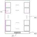
图1是本公开一个实施例提供的阵列基板的结构示意图。参见图1,该阵列基板包括显示区A1和周边电路区A2,该阵列基板还包括位于显示区A1内的若干个触控电极11。示例性地,图1中的周边电路区A2位于显示区A1的一侧,并且若干个触控电极11在显示区A1内排成多行多列。应理解的是,在可能的范围内,周边电路区A2可以位于显示区A1相对的两侧,在又一示例中周边电路区A2还可以环绕在显示区A1四周;在可能的范围内,若干个触控电极11可以按照任意一种平面内的单元排布方式进行排列,例如排列成倾斜网格、三角网格、菱形网格等等。FIG. 1 is a schematic structural diagram of an array substrate provided by an embodiment of the present disclosure. Referring to FIG. 1, the array substrate includes a display area A1 and a peripheral circuit area A2, and the array substrate further includes a plurality of
示例性地,图1中还示出了位于周边电路区A2中的触控电路21,该触控电路21被配置为通过采集若干个触控电极11上的电信号来实现触摸感测。应理解的是,出于触摸感测的应用需求,触控电路21与若干个触控电极11之间应当具有电路连接关系;然而为了图示清晰,图1中未示出将若干个触控电极11连接至周边电路区A2的若干条触控信号线12。其中应理解的是,基于图1中触控电路21位于显示区A1一侧的位置关系,上述若干条触控信号线12的延伸方向均为从显示区A1指向周边电路区A2的方向。Exemplarily, FIG. 1 also shows the
图2是本公开一个实施例提供的阵列基板的显示区内部走线示意图。图2中示例性地示出了排成两行两列的四个触控电极11,以及与这四个触控电极11对应的四条触控信号线12。本实施例中,阵列基板除了上述若干个触控电极11和若干条触控信号线12之外,还包括若干条第一导体线13和若干条第二导体线14,以及多行栅线GL和多列数据线DL。如图2所示,阵列基板中的所述若干条触控信号线12均具有相同的延伸方向,并且每条第一导体线13的延伸方向均与若干条触控信号线12的延伸方向相同,每条第二导体线14的延伸方向均与若干条触控信号线12的延伸方向不同。在连接关系上,每条第一导体线13在一个触控电极11的厚度方向上与该触控电极11相连;每条第二导体线14与一个触控电极11相对应,任一第二导体线14连接所对应的触控电极11所连接的触控信号线12,任一第二导体线14分别连接所对应的触控电极11所连接的每条第一导体线13。FIG. 2 is a schematic diagram of internal wirings in a display area of an array substrate according to an embodiment of the present disclosure. FIG. 2 exemplarily shows four
可以看出,基于第一导体线13和第二导体线14的设置,触控电极上11上的触控信号不仅能够直接传导至触控信号线12上,还能够通过第一导体线13和第二导体线14传输至触控信号线12上,而且触控电极11上各个位置到触控信号线12的电阻也得以均匀化。即,本公开实施例能够扩大触控信号线与触控电极之间相互接触的位置范围,并可以减小触控电极的边缘到触控信号线之间的电阻,因而可以提升通过触控电极接收到的触控信号的信号强度,有助于减少相关的触控不良,提升产品的触控性能。It can be seen that, based on the arrangement of the
示例性地,若干条第二导体线14与多行栅线GL在同一次构图工艺中形成,而若干条第一导体线13、若干条触控信号线12以及多列数据线DL在同一次构图工艺中形成。如此,第二导体线14和栅线GL位于同一层中,第一导体线13、触控信号线12以及数据线DL位于同一层中。Exemplarily, several
示例性地,阵列基板还包括第一绝缘层(在图2中省略表示),多行栅线GL和多列数据线DL分别位于该第一绝缘层的厚度方向上的两侧。如此,以第一绝缘层包括栅绝缘层的底栅结构为例,第二导体线14和栅线GL位于第一绝缘层的下侧,而第一导体线13、触控信号线12以及数据线DL位于第一绝缘层的上侧。Exemplarily, the array substrate further includes a first insulating layer (not shown in FIG. 2 ), and a plurality of rows of gate lines GL and a plurality of columns of data lines DL are located on both sides of the first insulating layer in the thickness direction, respectively. In this way, taking the bottom gate structure in which the first insulating layer includes a gate insulating layer as an example, the
示例性地,第一绝缘层中设有第一过孔15,每条第二导体线14通过第一过孔15连接所对应的第一导体线13和触控信号线12。如此,上述触控信号线12与第二导体线14之间的连接关系,以及上述第一导体线13与第二导体线14之间的连接关系,均可以通过彼此间正投影相交位置处的第一过孔15来实现。Exemplarily, a first via
示例性地,阵列基板还包括第二绝缘层(在图2中省略表示),若干个触控信号线12和若干个触控电极11分别位于第二绝缘层在厚度方向上的两侧。如此,以触控电极11位于第二绝缘层远离第一绝缘层的一侧为例,第一导体线13、触控信号线12以及数据线DL位于第二绝缘层的下侧,而触控电极11位于第二绝缘层的上侧。应理解的是,上述示例中的若干个触控电极11可以作为提供公共电压的公共电极来使用。Exemplarily, the array substrate further includes a second insulating layer (not shown in FIG. 2 ), and a plurality of
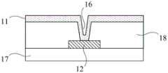
示例性地,第二绝缘层中设有若干个第二过孔16,每条触控信号线12通过至少一个第二过孔16与对应的触控电极11连接,每条第一导体线13通过至少一个的第二过孔16与对应的触控电极11连接。如此,上述触控信号线12与触控电极11之间的连接关系,以及上述第一导体线13与触控电极11之间的连接关系,均可以通过至少一个第二过孔16来实现。Exemplarily, a plurality of second via
图3是本公开一个实施例提供的阵列基板在第一过孔处的剖面示意图,图4是本公开一个实施例提供的阵列基板在第二过孔处的剖面示意图。对照图2可以看出,图3示出的是图2中标记“15”所指位置处的行向剖面,图4示出的是图2中标记“16”所指位置处的行向剖面。可以看出,与上述示例所述的一致,第二导体线14位于第一绝缘层17的下侧,而第一导体线13和触控信号线12位于第一绝缘层17的上侧;第一绝缘层17中设有第一过孔15,第二导体线14通过第一过孔15连接所对应的第一导体线13;第一导体线13和触控信号线12位于第二绝缘层18的下侧,而触控电极11位于第二绝缘层18的上侧;第二绝缘层18中设有若干个第二过孔16,触控信号线12通过第二过孔16与对应的触控电极11连接。3 is a schematic cross-sectional view of an array substrate provided at an embodiment of the present disclosure at a first via hole, and FIG. 4 is a cross-sectional schematic view of an array substrate provided by an embodiment of the present disclosure at a second via hole. It can be seen from Fig. 2 that Fig. 3 shows the row section at the position indicated by the mark "15" in Fig. 2, and Fig. 4 shows the row section at the position indicated by the mark "16" in Fig. 2 . It can be seen that, consistent with the above examples, the
图2中,按照从左至右的顺序,四条触控信号线12分别连接左上、左下、右上、右下的触控电极11,连接关系可以通过第二过孔16的设置得以体现。以此为例,阵列基板中的每条触控信号线12都将一个触控电极11连接至周边电路区,以在满足触控信号采集需求的同时使各触控电极11之间保持电性绝缘,避免不同触控电极11上的触控信号彼此干扰。比照图1和图2可以理解的是,为了使每个触控电极11上的触控信号都能单独地传输至周边电路区A2,每列触控电极11的行向投影范围都要能够容纳足够多的触控信号线12在其中平行排列,即触控电极11的尺寸、触控信号线12的线宽以及触控信号线12的排列间距均需要满足相对应的限制条件。In FIG. 2 , the four
例如,图5中示出了排成3行4列的触控电极11,由于每条触控信号线12都需要沿着列向将所连接的触控电极11上的触控信号引接至周边电路区A2,因此每列触控电极11的行向投影范围都要能够容纳至少3条触控信号线12在其范围内平行排列。可理解的是,本示例中每列触控电极11对应设置的触控信号线12的条数应当不少于触控电极11的总行数,而在大于触控电极11的总行数时会出现部分触控电极连接两条或两条以上的触控信号线12的情况。在一个示例中,可以设置远离触控电路21的触控电极11连接多于一条的触控信号线12,以在一定程度上补偿远端触控电极11上触控信号的电阻压降。For example, FIG. 5 shows the
图6示出了在图5所示结构基础上进行常规布线简化之后的结构,比照图5和图6可以看出的是,上述常规布线简化实际上是保留了触控信号的实际传输路径,而去除了触控信号线12中没有起到传输作用的部分走线。由于这一变化可以仅通过修改触控信号线所在导体膜层所对应的掩膜板图案来实现,因此可以不对原有的制作工艺造成很大影响。如此,有利地省去了多余走线的布线空间,避免了多余走线容易引发短路或串扰等不良的问题。相关技术中,图6所示的方式是最直观而常见的布线方式。Fig. 6 shows the structure after the conventional wiring is simplified on the basis of the structure shown in Fig. 5. It can be seen from Fig. 5 and Fig. 6 that the conventional wiring is simplified in fact to retain the actual transmission path of the touch signal, However, some traces in the
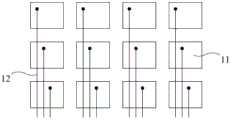
图7示出了本公开实施例在图5所示结构基础上进行布线简化之后的结构,比照图6和图7可以看出的是,本公开实施例中并没有完全去除触控信号线12中没有起到传输作用的部分走线,而是去除了该部分走线中处于相邻两行的触控电极11之间的部分(同样可以通过修改触控信号线所在导体膜层所对应的掩膜板图案来实现),从而有利地利用触控信号线的制作工艺形成了上述有助于将触控信号从触控电极11传导至触控信号线12上的第一导体线13。FIG. 7 shows the structure of the embodiment of the present disclosure after the wiring is simplified on the basis of the structure shown in FIG. 5 . It can be seen from FIG. 6 and FIG. 7 that the
然而应当理解的是,直接从触控信号线12上分离出来的第一导体线13在未经过其他连接设置的情况下仍为不具有任何有用功能的导体线。为叙述方便,本文将此类脱离于上述若干条触控信号线以外的与任一条触控信号线处于同一条直线上的导体线称为无效触控信号线。可理解的是,第一导体线13并不一定全部都是无效触控信号线(例如图7中每个触控电极11的正投影范围内最右侧的第一导体线13就不是无效触控信号线),而且不同位置处的触控电极11的正投影范围内无效触控信号线的数量也可能存在差异(如图7所示)。此外可以看出的是,图2中右上方触控电极11所在区域中以标记“13”示出的第一导体线13即属于无效触控信号线。However, it should be understood that the
本公开实施例中,为了实现上述提升触控信号的信号强度的效果,如图7所示的第一导体线13还需要与所对应的触控电极11和所对应的触控信号线12相连。其中,第一导体线13与触控电极11的连接方式可以参照触控信号线12与触控电极11的连接方式来实现,例如上文所述的那样将第二绝缘层中用于连接触控信号线12和触控电极11的第二过孔16扩展设置到第一导体线13和触控电极11之间,以在不增加工艺步骤的情况下实现上述连接关系。第一导体线13与触控信号线12之间可以借助行向延伸的第二导体线14来彼此相连,如图8所示,可以在每个触控电极11中央设置一条行向延伸的第二导体线14,并且该第二导体线14与每一条相交的第一导体线13及触控信号线12相连,使得第一导体线13能够连接到所对应的触控信号线12。In the embodiment of the present disclosure, in order to achieve the above effect of enhancing the signal strength of the touch signal, the
需要说明的是,第二导体线14除了可以单独制作在阵列基板内部之外,还可以如上文所述的那样与栅线GL在同一次构图工艺中形成(可参照阵列基板的双栅线设计),或者还可以与触控信号线12及第一导体线13在同一次构图工艺中形成,均能够实现上述提升触控信号的信号强度的效果。相比于其他两种方式,若干条触控信号线12、若干条第一导体线13以及若干条第二导体线14均在同一次构图工艺中形成所需要制作的过孔数量更少,更有助于提升触控信号的信号强度。It should be noted that the
可以看出,图2和图8分别给出了两种第二导体线的设置方式示例。图2中,与一个触控电极11所连接的所有的第一导体线13的第二导体线14的数量为两条,这两条第二导体线14的正投影分别位于该触控电极11的正投影区域的一个边缘(在图2中分别位于其上边缘和下边缘)。图8中,与一个触控电极11所连接的所有的第一导体线13的第二导体线14的数量为一条,该条第二导体线14的正投影位于该触控电极11的正投影区域的中央。It can be seen that FIG. 2 and FIG. 8 respectively give two examples of the arrangement of the second conductor lines. In FIG. 2 , the number of the
还需要说明的是,在上述任意一个示例中,显示区A1均可以包括多行多列的像素开口区,并且每条触控信号线12均位于相邻两列的像素开口区之间,每条第一导体线13均位于相邻两列的像素开口区之间,每条第二导体线14均位于相邻两行的像素开口区之间。如此,可以将触控信号线12、第一导体线13和第二导体线14均设置在黑矩阵所遮挡的区域范围内,减小对显示效果造成的影响。在一个示例中,每条触控信号线12在相邻两列像素开口区之间与数据线DL并行排列,而每条第一导体线13均为从一条触控信号线12上分离出来的无效触控信号线,触控信号线12、第一导体线13和数据线DL均处于阵列基板的源漏导电层当中。而且,每条第二导体线14在相邻两行像素开口区之间与栅线GL并行排列,第二导体线14和栅线GL均处于阵列基板的栅极导电层当中。It should also be noted that, in any of the above examples, the display area A1 may include pixel opening areas of multiple rows and columns, and each
还需要说明的是,上述示例中,与一个触控电极11相连的所有的第一导体线13的正投影均位于该触控电极11的正投影区域内,并且与一个触控电极11所连接的所有的第一导体线13相连的第二导体线14的正投影位于该触控电极11的正投影区域内。如此,可以避免相邻的触控电极11上触控信号的相互干扰,更有助于触控性能的提升。It should also be noted that, in the above example, the orthographic projections of all the
应理解的是,以上示例均为本公开的示例性说明,在相关技术中任意一种利用若干条触控信号线将若干个触控电极引接至显示区之外的方案的基础上均可能应用本公开的技术方案,以通过第一导体线和第二导体线的相关设置扩大触控信号线与触控电极之间相互接触的位置范围,从而提升通过触控电极接收到的触控信号的信号强度,有助于减少相关的触控不良,提升产品的触控性能。It should be understood that the above examples are all exemplary illustrations of the present disclosure, and may be applied on the basis of any solution in the related art that utilizes several touch signal lines to lead several touch electrodes outside the display area The technical solution of the present disclosure expands the position range of the mutual contact between the touch signal line and the touch electrode through the relative arrangement of the first conductor line and the second conductor line, thereby improving the sensitivity of the touch signal received through the touch electrode. Signal strength can help reduce related touch failures and improve the touch performance of products.
基于同样的发明构思,图9是本公开一个实施例提供的阵列基板的制造方法的步骤流程示意图。参见图9,该方法包括:Based on the same inventive concept, FIG. 9 is a schematic flowchart of steps of a method for manufacturing an array substrate provided by an embodiment of the present disclosure. Referring to Figure 9, the method includes:
步骤701、形成若干条触控信号线。
其中,所述若干条触控信号线具有相同的延伸方向。Wherein, the plurality of touch signal lines have the same extension direction.
步骤702、形成若干条第一导体线。
其中,所述若干条第一导体线的延伸方向与所述若干条触控信号线相同。Wherein, the extension direction of the plurality of first conductor lines is the same as that of the plurality of touch signal lines.
步骤703、形成若干条第二导体线。
其中,所述若干条第二导体线的延伸方向与所述若干条触控信号线不同。Wherein, the extending directions of the plurality of second conductor lines are different from those of the plurality of touch signal lines.
步骤704、形成若干个触控电极。
其中,所述若干个触控电极位于所述显示区内,所述若干条触控信号线将所述若干个触控电极连接至所述周边电路区。Wherein, the plurality of touch electrodes are located in the display area, and the plurality of touch signal lines connect the plurality of touch electrodes to the peripheral circuit area.
关于上述第一导体线和第二导体线,每条所述第一导体线在一个所述触控电极的厚度方向上与该触控电极相连;每条所述第二导体线与一个所述触控电极相对应,任一所述第二导体线连接所对应的触控电极所连接的触控信号线,任一所述第二导体线分别连接所对应的触控电极所连接的每条第一导体线。Regarding the above-mentioned first conductor lines and second conductor lines, each of the first conductor lines is connected to the touch electrode in the thickness direction of one of the touch electrodes; each of the second conductor lines is connected to one of the touch electrodes. Corresponding to the touch electrodes, any one of the second conductor lines is connected to the touch signal lines connected to the corresponding touch electrodes, and any one of the second conductor lines is respectively connected to each of the corresponding touch electrodes. the first conductor wire.
需要说明的是,上述步骤701至步骤704的执行顺序并不一定要严格按照如图9中所示出的那样,依照每个图形在阵列基板内部所在层的位置,可以适应性调整上述各步骤的执行顺序。It should be noted that, the execution order of the
由上述技术方案可知,本公开实施例基于第一导体线和第二导体线的设置,能够扩大触控信号线与触控电极之间相互接触的位置范围,并可以减小触控电极的边缘到触控信号线之间的电阻,因而可以提升通过触控电极接收到的触控信号的信号强度,有助于减少相关的触控不良,提升产品的触控性能。As can be seen from the above technical solutions, based on the arrangement of the first conductor lines and the second conductor lines, the embodiments of the present disclosure can expand the range of the mutual contact positions between the touch signal lines and the touch electrodes, and can reduce the edge of the touch electrodes. Therefore, the signal strength of the touch signal received through the touch electrodes can be improved, which is helpful to reduce related touch defects and improve the touch performance of the product.
在一个示例中,参照图2,上述阵列基板的制造方法具体包括以下过程:In one example, referring to FIG. 2 , the above-mentioned manufacturing method of the array substrate specifically includes the following processes:
第一次构图工艺:在衬底基板上形成包括栅极导电层的图形。The first patterning process: forming a pattern including a gate conductive layer on the base substrate.
在一个示例中,在对衬底基板(材质例如是玻璃、硅片、有机聚合物等等)的表面进行清洗和烘干之后,在衬底基板的表面上采用金属材料的物理气相沉积工艺(PhysicalVapor Deposition,PVD)沉积一层金属材料薄膜,膜层厚度等参数的设置可以通过例如调整相关工艺参数的手段来实现。在此基础之上,对整面分布的金属材料薄膜进行图案化处理:在还未图案化的金属材料薄膜上采用例如旋涂的方式涂覆一层光刻胶(此处以正性光刻胶为例进行说明),采用紫外光透过掩膜板照射全部待刻蚀区域内的光刻胶以使其充分曝光,再将其置于显影液中以通过显影将待刻蚀区域内的光刻胶全部去除,将余留下来的光刻胶作为掩膜对未图案化的栅极导电层进行刻蚀,刻蚀完成后再去除剩余的光刻胶。In one example, after cleaning and drying the surface of the base substrate (such as glass, silicon wafer, organic polymer, etc.), a physical vapor deposition process of metal material is used on the surface of the base substrate ( Physical Vapor Deposition, PVD) deposits a thin film of metal material, and the setting of parameters such as the thickness of the film layer can be achieved by means of, for example, adjusting relevant process parameters. On this basis, patterning treatment is performed on the metal material film distributed on the entire surface: a layer of photoresist (here, a positive photoresist is applied to the unpatterned metal material film by means of spin coating, for example) Example to illustrate), use ultraviolet light to pass through the mask to irradiate the photoresist in all the areas to be etched to make it fully exposed, and then place it in the developing solution to develop the photoresist in the area to be etched through development. The photoresist is completely removed, and the remaining photoresist is used as a mask to etch the unpatterned gate conductive layer, and after the etching is completed, the remaining photoresist is removed.
栅极导电层的形成材料可以是例如包括铁、铜、铝、钼、镍、钛、银、锌、锡、铅、铬、锰中至少一个元素的金属材料,并可以依照所期望的电导率设置组分。所述栅极导电层中包括上述栅线GL和上述若干条第二导体线14,还包括阵列基板中薄膜晶体管的栅电极。The material for forming the gate conductive layer can be, for example, a metal material including at least one element of iron, copper, aluminum, molybdenum, nickel, titanium, silver, zinc, tin, lead, chromium, and manganese, and can be formed according to desired electrical conductivity. Set components. The gate conductive layer includes the above-mentioned gate line GL and the above-mentioned several second conductor lines 14, and also includes the gate electrode of the thin film transistor in the array substrate.
第二次构图工艺:在形成第一绝缘层之后,形成包括第一过孔的图形。The second patterning process: after forming the first insulating layer, a pattern including the first via hole is formed.
在一个示例中,在衬底基板和栅极导电层之上采用化学气相沉积工艺(ChemicalVapor Deposition,CVD)沉积覆盖在基板和栅极导电层上的栅绝缘层(作为第一绝缘层),其中栅绝缘层的膜层厚度可能需要满足对于薄膜晶体管的栅绝缘层的厚度的相关要求,对于膜层厚度等参数的设置可以通过例如调整相关工艺参数的手段来实现。在此基础之上,在还未形成第一过孔15的第一绝缘层上采用例如旋涂的方式涂覆一层光刻胶(此处以正性光刻胶为例进行说明),采用紫外光透过掩膜板照射全部待刻蚀区域内的光刻胶以使其充分曝光,再将其置于显影液中以通过显影将待刻蚀区域内的光刻胶全部去除,将余留下来的光刻胶作为掩膜对还未形成第一过孔15的第一绝缘层进行刻蚀,以在第一绝缘层中形成包括第一过孔15的图形,刻蚀完成后再去除剩余的光刻胶。In one example, a gate insulating layer (as the first insulating layer) covering the substrate and the gate conductive layer is deposited by chemical vapor deposition (Chemical Vapor Deposition, CVD) on the base substrate and the gate conductive layer, wherein The film thickness of the gate insulating layer may need to meet relevant requirements for the thickness of the gate insulating layer of the thin film transistor, and the setting of parameters such as the film thickness can be achieved by, for example, adjusting relevant process parameters. On this basis, a layer of photoresist is applied on the first insulating layer where the first via
第三次构图工艺:形成包括有源层的图形。The third patterning process: forming a pattern including the active layer.
在一个示例中,在第一绝缘层上形成半导体材料层,并对半导体材料层进行图案化处理,以形成具有预期图案的有源层。其中,形成有源层的半导体材料可以包括非晶硅、多晶硅、单晶硅、金属氧化物半导体等等,并可以依照所要实现的薄膜晶体管的特性对至少部分区域进行掺杂。In one example, a semiconductor material layer is formed on the first insulating layer, and the semiconductor material layer is patterned to form an active layer having a desired pattern. The semiconductor material for forming the active layer may include amorphous silicon, polycrystalline silicon, single crystal silicon, metal oxide semiconductor, etc., and at least part of the region may be doped according to the characteristics of the thin film transistor to be realized.
第四次构图工艺:形成包括源漏导电层的图形。The fourth patterning process: forming a pattern including the source-drain conductive layer.
在一个示例中,在第一绝缘层和有源层上采用金属材料的物理气相沉积工艺沉积还未图案化的源漏导电层,膜层厚度等参数的设置可以通过例如调整相关工艺参数的手段来实现。在此基础之上,对整面分布的源漏导电层进行图案化处理:在还未图案化的源漏导电层上采用例如旋涂的方式涂覆一层光刻胶(此处以正性光刻胶为例进行说明),采用紫外光透过掩膜板照射全部待刻蚀区域内的光刻胶以使其充分曝光,再将其置于显影液中以通过显影将待刻蚀区域内的光刻胶全部去除,将余留下来的光刻胶作为掩膜对未图案化的源漏导电层进行刻蚀,刻蚀完成后再去除剩余的光刻胶。In one example, a physical vapor deposition process of a metal material is used to deposit an unpatterned source-drain conductive layer on the first insulating layer and the active layer, and parameters such as film thickness can be set by, for example, adjusting relevant process parameters. to fulfill. On this basis, patterning is performed on the source-drain conductive layers distributed over the entire surface: a layer of photoresist (here, positive photoresist is applied to the unpatterned source-drain conductive layers by means of spin coating, for example) The photoresist in the area to be etched is fully exposed by ultraviolet light through the mask plate to make it fully exposed, and then it is placed in the developer to develop the photoresist in the area to be etched by developing. All the photoresist is removed, and the remaining photoresist is used as a mask to etch the unpatterned source-drain conductive layer, and after the etching is completed, the remaining photoresist is removed.
源漏导电层的形成材料可以是例如包括铁、铜、铝、钼、镍、钛、银、锌、锡、铅、铬、锰中至少一个元素的金属材料,并可以依照所期望的电导率设置组分。所述源漏导电层中包括上述数据线DL、上述若干条触控信号线12和上述若干条第一导体线13,以及薄膜晶体管的源电极和漏电极。并且,第二导体线14与触控信号线12之间的连接以及第二导体线14与第一导体线13之间的连接已通过第一过孔15实现。The material for forming the source-drain conductive layer may be, for example, a metal material including at least one element of iron, copper, aluminum, molybdenum, nickel, titanium, silver, zinc, tin, lead, chromium, and manganese, and may be formed according to desired electrical conductivity. Set components. The source-drain conductive layer includes the data line DL, the plurality of
第五次构图工艺,在形成第二绝缘层后,形成包括第二过孔的图形。In the fifth patterning process, after forming the second insulating layer, a pattern including the second via hole is formed.
在一个示例中,在第一绝缘层和源漏导电层之上采用化学气相沉积工艺沉积覆盖在第一绝缘层和源漏导电层上的第二绝缘层。在此基础之上,在还未形成第二过孔16的第二绝缘层上采用例如旋涂的方式涂覆一层光刻胶(此处以正性光刻胶为例进行说明),采用紫外光透过掩膜板照射全部待刻蚀区域内的光刻胶以使其充分曝光,再将其置于显影液中以通过显影将待刻蚀区域内的光刻胶全部去除,将余留下来的光刻胶作为掩膜对还未形成第二过孔16的第二绝缘层进行刻蚀,以在第二绝缘层中形成包括第二过孔16的图形,刻蚀完成后再去除剩余的光刻胶。In one example, a chemical vapor deposition process is used to deposit a second insulating layer overlying the first insulating layer and the source-drain conductive layer over the first insulating layer and the source-drain conductive layer. On this basis, a layer of photoresist is applied on the second insulating layer on which the second via
第六次构图工艺:形成包括第一透明导电层的图形。The sixth patterning process: forming a pattern including the first transparent conductive layer.
在一个示例中,在第二绝缘层上采用透明导电材料(可以包括铟锡氧化物ITO、石墨烯、金属网格、导电聚合物、纳米导电材料中至少一个,还可以是例如是银薄膜一类的半透明的导电材料,并可以不仅限于此)的物理气相沉积工艺沉积还未图案化的第一透明导电层的图形,膜层厚度等参数的设置可以通过例如调整相关工艺参数的手段来实现。在此基础之上,对整面分布的透明导电材料进行图案化处理:在还未图案化的第一透明导电层上采用例如旋涂的方式涂覆一层光刻胶(此处以正性光刻胶为例进行说明),采用紫外光透过掩膜板照射全部待刻蚀区域内的光刻胶以使其充分曝光,再将其置于显影液中以通过显影将待刻蚀区域内的光刻胶全部去除,将余留下来的光刻胶作为掩膜对未图案化的第一透明导电层进行刻蚀,刻蚀完成后再去除剩余的光刻胶。第一透明导电层中,包括上述若干个触控电极11,并且触控电极11与触控信号线12之间的连接以及触控电极11与第一导体线13之间的连接已通过第二过孔16实现。In one example, a transparent conductive material (which may include at least one of indium tin oxide (ITO), graphene, metal mesh, conductive polymer, nano-conductive material, and may also be, for example, a silver thin film—is used on the second insulating layer. The pattern of the first transparent conductive layer that has not been patterned is deposited by the physical vapor deposition process of the semi-transparent conductive material, and can not be limited to this. The setting of parameters such as film thickness can be adjusted by means of, for example, adjusting the relevant process parameters. accomplish. On this basis, patterning treatment is performed on the transparent conductive material distributed on the entire surface: a layer of photoresist (here, positive light is applied to the first transparent conductive layer that has not been patterned) is coated by spin coating, for example. The photoresist in the area to be etched is fully exposed by ultraviolet light through the mask plate to make it fully exposed, and then it is placed in the developer to develop the photoresist in the area to be etched by developing. All the photoresist is removed, and the remaining photoresist is used as a mask to etch the unpatterned first transparent conductive layer, and after the etching is completed, the remaining photoresist is removed. The first transparent conductive layer includes the above-mentioned plurality of
第七次构图工艺:在形成第三绝缘层后,形成包括源漏连接过孔的图形。The seventh patterning process: after forming the third insulating layer, a pattern including source-drain connection vias is formed.
在一个示例中,在第二绝缘层和第一透明导电层之上采用化学气相沉积工艺沉积覆盖在第二绝缘层和第一透明导电层上的第三绝缘层。在此基础之上,在还未形成源漏连接过孔的第三绝缘层上采用例如旋涂的方式涂覆一层光刻胶(此处以正性光刻胶为例进行说明),采用紫外光透过掩膜板照射全部待刻蚀区域内的光刻胶以使其充分曝光,再将其置于显影液中以通过显影将待刻蚀区域内的光刻胶全部去除,将余留下来的光刻胶作为掩膜对还未形成源漏连接过孔的第二绝缘层和第三绝缘层进行刻蚀,以在第二绝缘层和第三绝缘层中形成包括源漏连接过孔的图形,刻蚀完成后再去除剩余的光刻胶。In one example, a chemical vapor deposition process is used to deposit a third insulating layer overlying the second insulating layer and the first transparent conductive layer over the second insulating layer and the first transparent conductive layer. On this basis, a layer of photoresist is applied on the third insulating layer where the source-drain connection vias have not yet been formed, for example, by spin coating (here, positive photoresist is used as an example for description), and ultraviolet light is used as an example. The light penetrates the mask to irradiate the photoresist in all the areas to be etched to make it fully exposed, and then put it in the developing solution to remove all the photoresist in the area to be etched through development, and the remaining The lower photoresist is used as a mask to etch the second insulating layer and the third insulating layer that have not yet formed source-drain connection vias, so as to form source-drain connection vias in the second insulating layer and the third insulating layer. After the etching is completed, the remaining photoresist is removed.
第八次构图工艺:形成包括第二透明导电层的图形。Eighth patterning process: forming a pattern including the second transparent conductive layer.
在一个示例中,在第三绝缘层上采用透明导电材料的物理气相沉积工艺沉积还未图案化的第二透明导电层的图形,膜层厚度等参数的设置可以通过例如调整相关工艺参数的手段来实现。在此基础之上,对整面分布的透明导电材料进行图案化处理:在还未图案化的第二透明导电层上采用例如旋涂的方式涂覆一层光刻胶(此处以正性光刻胶为例进行说明),采用紫外光透过掩膜板照射全部待刻蚀区域内的光刻胶以使其充分曝光,再将其置于显影液中以通过显影将待刻蚀区域内的光刻胶全部去除,将余留下来的光刻胶作为掩膜对未图案化的第二透明导电层进行刻蚀,刻蚀完成后再去除剩余的光刻胶。第二透明导电层中,包括分别填满每个像素开口区域的若干个像素电极,并且像素电极通过源漏连接过孔与上述源电极或漏电极相连。In one example, a physical vapor deposition process of a transparent conductive material is used to deposit a pattern of the unpatterned second transparent conductive layer on the third insulating layer, and parameters such as film thickness can be set by, for example, adjusting relevant process parameters. to fulfill. On this basis, patterning the transparent conductive material distributed on the entire surface: apply a layer of photoresist (here, positive photoresist) on the unpatterned second transparent conductive layer by, for example, spin coating. The photoresist in the area to be etched is fully exposed by ultraviolet light through the mask plate to make it fully exposed, and then it is placed in the developer to develop the photoresist in the area to be etched by developing. All the photoresist is removed, and the remaining photoresist is used as a mask to etch the unpatterned second transparent conductive layer, and after the etching is completed, the remaining photoresist is removed. The second transparent conductive layer includes a plurality of pixel electrodes respectively filling the opening area of each pixel, and the pixel electrodes are connected to the source electrode or the drain electrode through a source-drain connection via hole.
此后,形成覆盖在第三绝缘层和第二透明导电层之上的平坦化层,即完成了本公开实施例的阵列基板的制作。应理解的是,根据产品类型的不同可以参考上述过程得到其他实现方式的制作方法,在此不再赘述。Thereafter, a planarization layer covering the third insulating layer and the second transparent conductive layer is formed, and the fabrication of the array substrate according to the embodiment of the present disclosure is completed. It should be understood that, according to different product types, the above-mentioned process may be referred to to obtain the manufacturing methods of other implementation manners, which will not be repeated here.
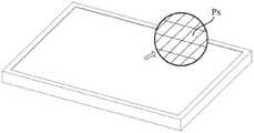
基于同样的公开构思,本公开实施例提供一种显示装置,该显示装置包括上述任意一种的阵列基板。本公开实施例中的显示装置可以为:显示面板、手机、平板电脑、电视机、显示器、笔记本电脑、数码相框、导航仪等任何具有显示功能的产品或部件。作为一种示例,图10是本公开一个实施例提供的显示装置的结构示意图。所述显示装置包括上述任意一种显示基板,该显示基板的显示区内包括行列设置的子像素区域Px,每个子像素区域Px中都设置有一个像素开口区域。基于第一导体线和第二导体线的设置,本公开实施例能够扩大触控信号线与触控电极之间相互接触的位置范围,并可以减小触控电极的边缘到触控信号线之间的电阻,因而可以提升通过触控电极接收到的触控信号的信号强度,有助于减少相关的触控不良,提升产品的触控性能。Based on the same disclosed concept, an embodiment of the present disclosure provides a display device including any one of the array substrates described above. The display device in the embodiment of the present disclosure may be any product or component with a display function, such as a display panel, a mobile phone, a tablet computer, a television, a monitor, a notebook computer, a digital photo frame, and a navigator. As an example, FIG. 10 is a schematic structural diagram of a display device provided by an embodiment of the present disclosure. The display device includes any one of the above-mentioned display substrates, and the display area of the display substrate includes sub-pixel regions Px arranged in rows and columns, and each sub-pixel region Px is provided with a pixel opening region. Based on the arrangement of the first conductor line and the second conductor line, the embodiment of the present disclosure can expand the range of the mutual contact position between the touch signal line and the touch electrode, and can reduce the distance between the edge of the touch electrode and the touch signal line. Therefore, the signal strength of the touch signal received through the touch electrodes can be improved, which is helpful to reduce related touch defects and improve the touch performance of the product.
需要说明的是,清晰起见,本公开的附图中仅示出了用于说明技术方案的结构;在实际产品中,还可以在可能的范围内在本公开附图的基础上进行添加、删除或变形,而不影响技术方案的实现。以上所述仅为本公开的实施例,并不用以限制本公开,凡在本公开的精神和原则之内,所作的任何修改、等同替换、改进等,均应包含在本公开的保护范围之内。It should be noted that, for the sake of clarity, the drawings of the present disclosure only show the structures used to illustrate the technical solutions; in actual products, additions, deletions or deformation without affecting the realization of the technical solution. The above description is only an embodiment of the present disclosure, and is not intended to limit the present disclosure. Any modification, equivalent replacement, improvement, etc. made within the spirit and principle of the present disclosure should be included in the protection scope of the present disclosure. Inside.
Claims (11)
Priority Applications (3)
| Application Number | Priority Date | Filing Date | Title |
|---|---|---|---|
| CN201810258988.XACN108446053B (en) | 2018-03-27 | 2018-03-27 | Array substrate, method for manufacturing the same, and display device |
| US16/473,718US20210333968A1 (en) | 2018-03-27 | 2018-11-30 | Array substrate and manufacturing method thereof, and display device |
| PCT/CN2018/118516WO2019184416A1 (en) | 2018-03-27 | 2018-11-30 | Array substrate and manufacturing method therefor, and display apparatus |
Applications Claiming Priority (1)
| Application Number | Priority Date | Filing Date | Title |
|---|---|---|---|
| CN201810258988.XACN108446053B (en) | 2018-03-27 | 2018-03-27 | Array substrate, method for manufacturing the same, and display device |
Publications (2)
| Publication Number | Publication Date |
|---|---|
| CN108446053A CN108446053A (en) | 2018-08-24 |
| CN108446053Btrue CN108446053B (en) | 2021-03-26 |
Family
ID=63196884
Family Applications (1)
| Application Number | Title | Priority Date | Filing Date |
|---|---|---|---|
| CN201810258988.XAActiveCN108446053B (en) | 2018-03-27 | 2018-03-27 | Array substrate, method for manufacturing the same, and display device |
Country Status (3)
| Country | Link |
|---|---|
| US (1) | US20210333968A1 (en) |
| CN (1) | CN108446053B (en) |
| WO (1) | WO2019184416A1 (en) |
Families Citing this family (4)
| Publication number | Priority date | Publication date | Assignee | Title |
|---|---|---|---|---|
| CN108446053B (en)* | 2018-03-27 | 2021-03-26 | 京东方科技集团股份有限公司 | Array substrate, method for manufacturing the same, and display device |
| CN114981762B (en)* | 2020-10-22 | 2024-08-13 | 京东方科技集团股份有限公司 | Array substrate, manufacturing method thereof and display device |
| CN112864199B (en)* | 2021-01-08 | 2022-12-06 | 武汉华星光电半导体显示技术有限公司 | Touch display panel and display device |
| CN117016053A (en)* | 2022-03-01 | 2023-11-07 | 京东方科技集团股份有限公司 | Display panel, preparation method thereof and display device |
Citations (6)
| Publication number | Priority date | Publication date | Assignee | Title |
|---|---|---|---|---|
| CN103760708A (en)* | 2014-01-09 | 2014-04-30 | 北京京东方光电科技有限公司 | Array substrate, capacitive touch screen and touch display device |
| CN105677076A (en)* | 2015-12-28 | 2016-06-15 | 上海天马微电子有限公司 | Touch display device, touch display panel and array substrate |
| CN106055171A (en)* | 2016-08-08 | 2016-10-26 | 京东方科技集团股份有限公司 | Array substrate, manufacturing method thereof and display device |
| CN107229153A (en)* | 2017-07-07 | 2017-10-03 | 昆山龙腾光电有限公司 | Embedded touch control type array base palte and preparation method and display device |
| CN107340919A (en)* | 2017-06-30 | 2017-11-10 | 厦门天马微电子有限公司 | Array base palte, display panel and display device |
| CN107422930A (en)* | 2017-05-02 | 2017-12-01 | 京东方科技集团股份有限公司 | Touch base plate and touch-screen |
Family Cites Families (7)
| Publication number | Priority date | Publication date | Assignee | Title |
|---|---|---|---|---|
| CN101118470B (en)* | 2006-08-02 | 2010-12-29 | 智点科技(深圳)有限公司 | Touch control type flat-panel display electric pole structure |
| TWI376623B (en)* | 2008-11-19 | 2012-11-11 | Au Optronics Corp | Touch panel and touch display panel |
| KR101843462B1 (en)* | 2011-12-14 | 2018-03-30 | 엘지디스플레이 주식회사 | Liquid crystal display apparatus comprising a touch screen |
| CN103472943A (en)* | 2013-08-06 | 2013-12-25 | 福建华映显示科技有限公司 | Embedded touch control display panel |
| CN104678628A (en)* | 2013-11-26 | 2015-06-03 | 瀚宇彩晶股份有限公司 | Embedded touch display panel and driving method thereof |
| CN107490913B (en)* | 2015-04-01 | 2020-11-13 | 上海天马微电子有限公司 | Array substrate, display panel and display device |
| CN108446053B (en)* | 2018-03-27 | 2021-03-26 | 京东方科技集团股份有限公司 | Array substrate, method for manufacturing the same, and display device |
- 2018
- 2018-03-27CNCN201810258988.XApatent/CN108446053B/enactiveActive
- 2018-11-30WOPCT/CN2018/118516patent/WO2019184416A1/ennot_activeCeased
- 2018-11-30USUS16/473,718patent/US20210333968A1/ennot_activeAbandoned
Patent Citations (6)
| Publication number | Priority date | Publication date | Assignee | Title |
|---|---|---|---|---|
| CN103760708A (en)* | 2014-01-09 | 2014-04-30 | 北京京东方光电科技有限公司 | Array substrate, capacitive touch screen and touch display device |
| CN105677076A (en)* | 2015-12-28 | 2016-06-15 | 上海天马微电子有限公司 | Touch display device, touch display panel and array substrate |
| CN106055171A (en)* | 2016-08-08 | 2016-10-26 | 京东方科技集团股份有限公司 | Array substrate, manufacturing method thereof and display device |
| CN107422930A (en)* | 2017-05-02 | 2017-12-01 | 京东方科技集团股份有限公司 | Touch base plate and touch-screen |
| CN107340919A (en)* | 2017-06-30 | 2017-11-10 | 厦门天马微电子有限公司 | Array base palte, display panel and display device |
| CN107229153A (en)* | 2017-07-07 | 2017-10-03 | 昆山龙腾光电有限公司 | Embedded touch control type array base palte and preparation method and display device |
Also Published As
| Publication number | Publication date |
|---|---|
| WO2019184416A1 (en) | 2019-10-03 |
| US20210333968A1 (en) | 2021-10-28 |
| CN108446053A (en) | 2018-08-24 |
Similar Documents
| Publication | Publication Date | Title |
|---|---|---|
| CN108319397B (en) | Array substrate and touch display device | |
| CN106933416B (en) | An array substrate and its manufacturing method, a display panel and a display device | |
| CN108446053B (en) | Array substrate, method for manufacturing the same, and display device | |
| CN106681077B (en) | Display panel and display device | |
| CN108336100B (en) | Array substrate and preparation method thereof, display panel, and display device | |
| WO2015090000A1 (en) | Array substrate and manufacturing method therefor, and display device | |
| WO2014044054A1 (en) | Tft array substrate, fabrication method thereof, and liquid crystal display device | |
| CN204422935U (en) | A kind of array base palte and display device | |
| CN105159486A (en) | ADS array substrate, manufacturing method for ADS array substrate and display device | |
| CN105448935B (en) | A kind of array substrate and preparation method thereof, display device | |
| CN105093736A (en) | IPS array substrate, manufacture method thereof and display device | |
| CN101093843A (en) | Electrode structure in flat panel display, and fabricating method | |
| CN106876330A (en) | A kind of array base palte and preparation method thereof, display panel and display device | |
| US10534233B2 (en) | Array substrate, method for manufacturing the same, display device | |
| WO2020210939A1 (en) | Touch display substrate, manufacturing method therefor, and display device | |
| CN107845644B (en) | Array substrate, preparation method thereof and display device | |
| CN104795405B (en) | A kind of array base palte and preparation method thereof, display device | |
| CN106873266B (en) | Array substrate, liquid crystal display panel and display device | |
| CN106095167B (en) | Touch base plate and preparation method thereof, display device | |
| CN108535925B (en) | Display panels and display devices | |
| CN210668377U (en) | Display substrate and display device | |
| CN109117025B (en) | Display panel, method for making the same, and display device | |
| CN101577255A (en) | Method for manufacturing TFT array substrate | |
| CN117199080A (en) | Array substrate and production method thereof, display panel | |
| CN210324162U (en) | Embedded self-capacitive touch display substrate and touch display device |
Legal Events
| Date | Code | Title | Description |
|---|---|---|---|
| PB01 | Publication | ||
| PB01 | Publication | ||
| SE01 | Entry into force of request for substantive examination | ||
| SE01 | Entry into force of request for substantive examination | ||
| GR01 | Patent grant | ||
| GR01 | Patent grant |