CN108428760B - Efficient photovoltaic solder strip and manufacturing method thereof - Google Patents
Efficient photovoltaic solder strip and manufacturing method thereofDownload PDFInfo
- Publication number
- CN108428760B CN108428760BCN201810254457.3ACN201810254457ACN108428760BCN 108428760 BCN108428760 BCN 108428760BCN 201810254457 ACN201810254457 ACN 201810254457ACN 108428760 BCN108428760 BCN 108428760B
- Authority
- CN
- China
- Prior art keywords
- reflective
- base material
- tin
- copper
- copper base
- Prior art date
- Legal status (The legal status is an assumption and is not a legal conclusion. Google has not performed a legal analysis and makes no representation as to the accuracy of the status listed.)
- Active
Links
Images


Classifications
- H—ELECTRICITY
- H10—SEMICONDUCTOR DEVICES; ELECTRIC SOLID-STATE DEVICES NOT OTHERWISE PROVIDED FOR
- H10F—INORGANIC SEMICONDUCTOR DEVICES SENSITIVE TO INFRARED RADIATION, LIGHT, ELECTROMAGNETIC RADIATION OF SHORTER WAVELENGTH OR CORPUSCULAR RADIATION
- H10F19/00—Integrated devices, or assemblies of multiple devices, comprising at least one photovoltaic cell covered by group H10F10/00, e.g. photovoltaic modules
- H10F19/90—Structures for connecting between photovoltaic cells, e.g. interconnections or insulating spacers
- H10F19/902—Structures for connecting between photovoltaic cells, e.g. interconnections or insulating spacers for series or parallel connection of photovoltaic cells
- H10F19/906—Structures for connecting between photovoltaic cells, e.g. interconnections or insulating spacers for series or parallel connection of photovoltaic cells characterised by the materials of the structures
- H—ELECTRICITY
- H10—SEMICONDUCTOR DEVICES; ELECTRIC SOLID-STATE DEVICES NOT OTHERWISE PROVIDED FOR
- H10F—INORGANIC SEMICONDUCTOR DEVICES SENSITIVE TO INFRARED RADIATION, LIGHT, ELECTROMAGNETIC RADIATION OF SHORTER WAVELENGTH OR CORPUSCULAR RADIATION
- H10F19/00—Integrated devices, or assemblies of multiple devices, comprising at least one photovoltaic cell covered by group H10F10/00, e.g. photovoltaic modules
- H10F19/90—Structures for connecting between photovoltaic cells, e.g. interconnections or insulating spacers
- H10F19/902—Structures for connecting between photovoltaic cells, e.g. interconnections or insulating spacers for series or parallel connection of photovoltaic cells
- H10F19/904—Structures for connecting between photovoltaic cells, e.g. interconnections or insulating spacers for series or parallel connection of photovoltaic cells characterised by the shapes of the structures
- H—ELECTRICITY
- H10—SEMICONDUCTOR DEVICES; ELECTRIC SOLID-STATE DEVICES NOT OTHERWISE PROVIDED FOR
- H10F—INORGANIC SEMICONDUCTOR DEVICES SENSITIVE TO INFRARED RADIATION, LIGHT, ELECTROMAGNETIC RADIATION OF SHORTER WAVELENGTH OR CORPUSCULAR RADIATION
- H10F77/00—Constructional details of devices covered by this subclass
- H10F77/40—Optical elements or arrangements
- H10F77/42—Optical elements or arrangements directly associated or integrated with photovoltaic cells, e.g. light-reflecting means or light-concentrating means
- H10F77/488—Reflecting light-concentrating means, e.g. parabolic mirrors or concentrators using total internal reflection
- Y—GENERAL TAGGING OF NEW TECHNOLOGICAL DEVELOPMENTS; GENERAL TAGGING OF CROSS-SECTIONAL TECHNOLOGIES SPANNING OVER SEVERAL SECTIONS OF THE IPC; TECHNICAL SUBJECTS COVERED BY FORMER USPC CROSS-REFERENCE ART COLLECTIONS [XRACs] AND DIGESTS
- Y02—TECHNOLOGIES OR APPLICATIONS FOR MITIGATION OR ADAPTATION AGAINST CLIMATE CHANGE
- Y02E—REDUCTION OF GREENHOUSE GAS [GHG] EMISSIONS, RELATED TO ENERGY GENERATION, TRANSMISSION OR DISTRIBUTION
- Y02E10/00—Energy generation through renewable energy sources
- Y02E10/50—Photovoltaic [PV] energy
- Y02E10/52—PV systems with concentrators
- Y—GENERAL TAGGING OF NEW TECHNOLOGICAL DEVELOPMENTS; GENERAL TAGGING OF CROSS-SECTIONAL TECHNOLOGIES SPANNING OVER SEVERAL SECTIONS OF THE IPC; TECHNICAL SUBJECTS COVERED BY FORMER USPC CROSS-REFERENCE ART COLLECTIONS [XRACs] AND DIGESTS
- Y02—TECHNOLOGIES OR APPLICATIONS FOR MITIGATION OR ADAPTATION AGAINST CLIMATE CHANGE
- Y02P—CLIMATE CHANGE MITIGATION TECHNOLOGIES IN THE PRODUCTION OR PROCESSING OF GOODS
- Y02P70/00—Climate change mitigation technologies in the production process for final industrial or consumer products
- Y02P70/50—Manufacturing or production processes characterised by the final manufactured product
Landscapes
- Photovoltaic Devices (AREA)
Abstract
Translated fromChinese
Description
Translated fromChinese技术领域technical field
本发明涉及太阳能电池组件加工技术领域,特别是一种高效光伏焊带及其制作方法。The invention relates to the technical field of solar cell component processing, in particular to a high-efficiency photovoltaic welding ribbon and a manufacturing method thereof.
背景技术Background technique
太阳能光伏发电是利用太阳光照射在半导体界面的光生伏特效应,将光能直接转变为电能的一种技术。目前常规的光伏组件,需要利用焊带将不同电池片串联起来,焊带一端焊接在电池正面,另一端焊接在另一电池背面,并封装进光伏组件,将光伏电池产生的电能导出到汇流条上,然后经过处理电路送到用户终端,达到组件功率输出目的。Solar photovoltaic power generation is a technology that uses the photovoltaic effect of sunlight irradiated on the semiconductor interface to directly convert light energy into electrical energy. At present, conventional photovoltaic modules need to use welding strips to connect different cells in series. One end of the welding strip is welded to the front of the battery, and the other end is welded to the back of another battery, and is packaged into the photovoltaic module to export the electrical energy generated by the photovoltaic cell to the bus bar. , and then sent to the user terminal through the processing circuit to achieve the purpose of component power output.
普通光伏焊带不具备反光效果,照射到其上的光能白白浪费掉了,反光光伏焊带具备反光功能,其将照射到其上的光全反射到发电单元,降低了发电功率的输出。Ordinary photovoltaic welding tape does not have a reflective effect, and the light energy irradiated on it is wasted in vain. The reflective photovoltaic welding tape has a reflective function, which fully reflects the light irradiated on it to the power generation unit, reducing the output of power generation.
现有的反光焊带主要结构为以铜芯为基础,在铜芯上表面(受光面)压延薄银层,下表面(非受光面)压延上锡铅层,银层具有特殊的反光织构,然后再裁剪成所需的焊带尺寸,此种焊带虽然能够提高组件的输出功率,但其本身具有以下缺点:1)成本昂贵,由于大量采用的贵金属银,其成本是常规焊带的数倍;2)需要开发新的焊接或者其他联结工艺,成本高;3)现有太阳能组件生产线的焊接工艺无法将铜芯上面的银层焊接至电池背面,需通过其他工艺联接,工艺复杂,成本高昂;4)由于裁剪后铜芯左右两边没有镀层保护,铜芯直接和组件中的 EVA 接触,增加了组件在日常使用中失效的概率;5)反光结构不合理,反光镀层成分不合适,反光焊带反光效果不理想,不能形成全反射,反光焊带生产过程中,反光结构不易达到设计要求。The main structure of the existing reflective welding tape is based on a copper core, a thin silver layer is rolled on the upper surface (light-receiving surface) of the copper core, and a tin-lead layer is rolled on the lower surface (non-light-receiving surface), and the silver layer has a special reflective texture. , and then cut to the required size of the ribbon. Although this ribbon can improve the output power of the component, it has the following disadvantages: 1) The cost is expensive. Due to the large amount of precious metal silver, the cost is the same as that of the conventional ribbon. 2) New welding or other connection processes need to be developed, and the cost is high; 3) The welding process of the existing solar module production line cannot weld the silver layer on the copper core to the back of the battery, and it needs to be connected by other processes, and the process is complicated. High cost; 4) Since there is no coating protection on the left and right sides of the copper core after cutting, the copper core is directly in contact with the EVA in the module, which increases the probability of failure of the module in daily use; 5) The reflective structure is unreasonable and the reflective coating composition is not suitable, The reflective effect of the reflective welding tape is not ideal, and total reflection cannot be formed. In the production process of the reflective welding tape, the reflective structure is not easy to meet the design requirements.
发明内容SUMMARY OF THE INVENTION
本发明需要解决的技术问题是提供了一种高效光伏焊带及其制作方法,以解决普通光伏焊带不具备反光效果而降低发电功率输出以及现有的反光焊带价格昂贵、反光结构不合理使得反光效果不理想的问题,以提高发电功率的输出。The technical problem to be solved by the present invention is to provide a high-efficiency photovoltaic welding strip and a manufacturing method thereof, so as to solve the problem that the ordinary photovoltaic welding strip does not have the reflective effect and reduces the power output, and the existing reflective welding strip is expensive and has an unreasonable reflective structure. The problem of making the reflection effect unsatisfactory in order to improve the output of power generation.
为解决上述技术问题,本发明所采取的技术方案如下。In order to solve the above technical problems, the technical solutions adopted by the present invention are as follows.
一种高效光伏焊带,包括铜基材以及通过风刀凃锡系统包覆设置在铜基材外的合金镀锡层,所述铜基材由多个铜基材基本单元依次首尾连接组成,相邻两铜基材基本单元之间形成用于进行图像识别的标记点;所述铜基材基本单元包括一体设置的铜基材反光段和铜基材背光段,所述铜基材反光段的上表面上设置有截面形状为等腰梯形结构的锯齿状沟槽,铜基材反光段的下表面上设置有弧形凹槽,所述铜基材背光段的上表面上设置有截面形状同锯齿状沟槽形状相同的锯齿状沟槽二;所述合金镀锡层包括涂设在锯齿状沟槽外层的反光面镀锡层、涂设在弧形凹槽外层用于与放置在铜基材反光段下方的第一电池片主栅线焊接连接的下焊接面镀锡层、涂设在铜基材背光段上表面用于与放置在铜基材背光段上方的第二电池片背电极焊接连接的上焊接面镀锡层。A high-efficiency photovoltaic welding tape includes a copper base material and an alloy tin plating layer which is covered and arranged outside the copper base material by an air knife tin coating system, wherein the copper base material is composed of a plurality of copper base material basic units connected end to end in sequence, Marking points for image recognition are formed between two adjacent basic units of copper substrates; the basic units of copper substrates include a copper substrate reflective segment and a copper substrate backlight segment that are integrally arranged, and the copper substrate reflective segment The upper surface of the copper substrate is provided with a zigzag groove with an isosceles trapezoid structure, the lower surface of the copper substrate reflective segment is provided with an arc groove, and the upper surface of the copper substrate backlight segment is provided with a cross-sectional shape. The
进一步优化技术方案,所述反光面镀锡层为均匀排列具有更好反光效果的倒等腰三角形结构。To further optimize the technical solution, the tin-plated layer on the reflective surface is an inverted isosceles triangular structure that is uniformly arranged and has better reflective effect.
进一步优化技术方案,所述合金镀锡层包括以下重量比例的组分:Sn 60~63%、Bi0~1%、P 0~1%、P 0~1%、GeP 0~1 %、Pb 36~37%。Further optimizing the technical scheme, the alloy tin plating layer includes the following components by weight: Sn 60~63%, Bi0~1%, P 0~1%, P 0~1%, GeP 0~1%, Pb 36 ~37%.
进一步优化技术方案,所述合金镀锡层包括以下重量比例的组分:Sn 63 %,Bi0.02 %,P 0.03 %,P 0.02 %,GeP 0.001 %,Pb 36.929 %。To further optimize the technical solution, the alloy tin plating layer includes the following components by weight: Sn 63%, Bi0.02%, P 0.03%, P 0.02%, GeP 0.001%, Pb 36.929%.
进一步优化技术方案,所述反光面镀锡层的厚度为3μm以下。The technical solution is further optimized, and the thickness of the tin plating layer on the reflective surface is 3 μm or less.
进一步优化技术方案,所述上焊接面镀锡层的厚度为20μm±5μm。Further optimizing the technical solution, the thickness of the tin-plated layer on the upper welding surface is 20 μm±5 μm.
进一步优化技术方案,所述下焊接面镀锡层的厚度为15μm±5μm。Further optimizing the technical solution, the thickness of the tin plating layer on the lower soldering surface is 15 μm±5 μm.
高效光伏焊带的制作方法,1)先将一定规格的无氧铜丝通过压延轮压到所需尺寸的无氧铜带;2)无氧铜带经过生产线上的模具整形机构使得无氧铜带形成多个铜基材基本单元,相邻两铜基材基本单元之间形成标记点,将铜基材基本单元分设为铜基材反光段和铜基材背光段,在铜基材反光段的反光面上形成设定结构的锯齿状沟槽以及边缘反光斜面,在铜基材反光段反光面的背面形成弧形凹槽,在铜基材背光段形成与铜基材反光段结构相同的锯齿状沟槽二;3)锡铅合金经过退火、清洗、熔化后,再经过精密风刀镀锡装置依次在铜基材反光段的上表面上形成反光面镀锡层、铜基材反光段的下表面上形成下焊接面镀锡层、铜基材背光段的上表面上形成上焊接面镀锡层,未涂锡的铜基材背光段背面形成背光面。The production method of high-efficiency photovoltaic welding tape is as follows: 1) First, a certain specification of oxygen-free copper wire is pressed to the required size of oxygen-free copper tape through a calendering wheel; 2) The oxygen-free copper tape passes through the mold shaping mechanism on the production line to make the oxygen-free copper tape. The tape forms a plurality of basic units of copper substrates, and a marking point is formed between the basic units of two adjacent copper substrates. The basic units of copper substrates are divided into copper substrate reflective sections and copper substrate backlight sections. A zigzag groove with a set structure and an edge reflective slope are formed on the reflective surface of the copper substrate, arc grooves are formed on the back of the reflective surface of the copper substrate reflective section, and the copper substrate backlight section is formed with the same structure as the copper substrate reflective section.
由于采用了以上技术方案,本发明所取得技术进步如下。Due to the adoption of the above technical solutions, the technical progress achieved by the present invention is as follows.
本发明设计独特、实用性强,通过将铜基材的上表面设置成等腰梯形结构,再将反光面镀锡层涂设在铜基材反光段中的锯齿状沟槽上的方式,使得反光面镀锡层在涂设的时候能够形成理想的等腰三角形结构,满足了设计要求,大大地提高了反光效果,从而有效地解决了光伏焊带反光效果差的问题;弧形凹槽的设置能够在反光焊带生产过程中,在弧形凹槽内形成一定量的镀层合金存留,以便使光伏焊带焊接可靠,同时弧形凹槽结构由于集肤效应作用可有效增大焊带的载流量,减小焊带在导电时的热损,提高组件功率输出;通过在想相邻两铜基材基本单元之间设置有标记点,能够进行图像识别。The invention has unique design and strong practicability. By setting the upper surface of the copper base material into an isosceles trapezoid structure, and then coating the tin-plated layer on the reflective surface on the zigzag grooves in the reflective section of the copper base material, the The tin-plated layer on the reflective surface can form an ideal isosceles triangular structure when it is coated, which meets the design requirements and greatly improves the reflective effect, thus effectively solving the problem of poor reflective effect of the photovoltaic ribbon; The setting can form a certain amount of coating alloy retention in the arc groove during the production process of the reflective welding strip, so that the photovoltaic welding strip can be welded reliably. At the same time, the arc groove structure can effectively increase the welding strip due to the skin effect. The current-carrying capacity can reduce the heat loss of the welding tape when conducting electricity, and improve the power output of the module. Image recognition can be performed by setting a marking point between the two adjacent copper substrate basic units.
附图说明Description of drawings
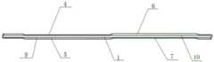
图1为本发明的侧视图;Fig. 1 is the side view of the present invention;
图2为本发明的俯视图;Fig. 2 is the top view of the present invention;
图3为图2的AA向剖视图;3 is a sectional view taken along the line AA of FIG. 2;
图4为图2的BB向剖视图;Fig. 4 is the BB direction sectional view of Fig. 2;
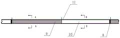
图5为本发明铜基材结构示意图。FIG. 5 is a schematic diagram of the structure of the copper substrate of the present invention.
其中:1、铜基材,2、锯齿状沟槽,3、弧形凹槽,4、反光面镀锡层,5、下焊接面镀锡层,6、上焊接面镀锡层,7、背光面,8、标记点,9、铜基材反光段,10、铜基材背光段,11、铜基材基本单元,12、锯齿状沟槽二。Among them: 1. Copper base material, 2. Sawtooth groove, 3. Arc-shaped groove, 4. Tin coating on reflective surface, 5. Tin coating on lower welding surface, 6. Tin coating on upper welding surface, 7. Backlight surface, 8. Marking point, 9. Reflective section of copper base material, 10. Backlight section of copper base material, 11. Basic unit of copper base material, 12.
具体实施方式Detailed ways
下面将结合具体实施例对本发明进行进一步详细说明。The present invention will be further described in detail below with reference to specific embodiments.
一种高效光伏焊带及其制作方法,结合图1至图2所示,包括铜基材1和合金镀锡层。A high-efficiency photovoltaic welding ribbon and a manufacturing method thereof, as shown in FIG. 1 to FIG. 2 , include a
铜基材1为双零3的无氧铜,铜的导电率较高,铜经过成型模具后成型能达到理想的角度并且表面光滑无毛刺,铜基材经过镀锡后能形成光滑的反光面。铜基材1由多个铜基材基本单元11依次首尾连接组成,相邻两铜基材基本单元11之间形成标记点8,标记点8用于进行图像识别。铜基材基本单元11包括铜基材反光段9和铜基材背光段10。铜基材反光段9的上表面上设置有锯齿状沟槽2,锯齿状沟槽2的截面形状为等腰梯形结构,等腰梯形的反光结构有助于在光伏焊带凃锡过程中经过凃锡而形成理想的等腰三角形结构,若是在铜基材上直接形成的是等腰三角形,那么在光伏焊带经过生产凃锡工序后,形成的等腰三角形达不到设计的等腰三角形角度,反光效果就不理想,不能形成全反射;铜基材反光段9的下表面上设置有弧形凹槽3,弧形凹槽结构的设计是为了在反光焊带生产过程中,在弧形凹槽内形成一定量的镀层合金存留,以便使光伏焊带焊接更加可靠,同时弧形凹槽结构由于集肤效应作用可有效增大焊带的载流量,减小焊带在导电时的热损,提高组件功率输出。铜基材背光段10的表面上设置有与铜基材反光段9上的锯齿状沟槽2结构相同的锯齿状沟槽二12。The
合金镀锡层镀设在铜基材1的表面上,设置为特定的厚度,镀层合金经过特殊加工,具有特定的成分,其成分含有特定比例的金属铋,金属铋的添加能够增加焊带表面的亮度,以加强焊带表面的反光效果;镀层合金含有特定比例的磷元素,其作用是增加镀层在热熔状态下的流动性,使反光焊带在镀锡工序中形成的沟槽表面锡层尽可能地薄,使在反光焊带生产过程中可靠稳定地形成设计角度的反光结构。本发明使用的锡合金流动性好、亮度高,能形成优质的反光面。The alloy tin plating layer is plated on the surface of the
合金镀锡层包括以下重量比例的组分:Sn 60~63%、Bi 0~1%、P 0~1%、P 0~1%、GeP0~1 %、Pb 36~37%。本实施例中合金镀锡层采用的重量比例的组分为Sn 63 %,Bi 0.02 %,P0.03 %,P 0.02 %,GeP 0.001 %,Pb 36.929 %。这种成分配比可大大增加合金的焊接拉力;增加合金镀层的亮度,提高反光效果;增加合金热熔状态下的流动性,使焊带表面合金镀层均匀平整,增加反光效果。The alloy tin plating layer includes the following components by weight: Sn 60~63%, Bi 0~1%, P 0~1%, P 0~1%, GeP0~1%, Pb 36~37%. In the present embodiment, the components of the alloy tin plating layer by weight are Sn 63%, Bi 0.02%, P0.03%, P 0.02%, GeP 0.001%, Pb 36.929%. This composition ratio can greatly increase the welding tension of the alloy; increase the brightness of the alloy coating and improve the reflective effect; increase the fluidity of the alloy in the hot-melting state, make the alloy coating on the surface of the welding strip uniform and smooth, and increase the reflective effect.
合金镀锡层包括反光面镀锡层4、下焊接面镀锡层5和上焊接面镀锡层6。反光面镀锡层4涂设在锯齿状沟槽2的外层,厚度为3μm以下,为均匀排列的倒等腰三角形结构,反光角度设计合理,对照射到其上的光能形成全反射,具有更好反光效果;下焊接面镀锡层5涂设在弧形凹槽3的外层,厚度为15μm±5μm,用于与放置在铜基材反光段9下方的第一电池片主栅线焊接连接,能够有效提高焊带的导电率;上焊接面镀锡层6涂设在铜基材背光段10上表面上,厚度为20μm±5μm,用于与放置在铜基材背光段10上方的第二电池片背电极焊接连接。The alloy tin-plated layer includes a tin-plated layer 4 on the reflective surface, a tin-plated
铜基材反光段9的截面图如图3所示,包括规则排列3μm以下的反光面镀锡层4,反光面镀锡层4为倒等腰三角形沟槽,反光面镀锡层4的下方为铜基材,铜基材的下方为15μm±5μm的下焊接面镀锡层。The cross-sectional view of the
铜基材背光段10的截面图如图4所示,包括铜基材,铜基材的上方设置有等腰梯形结构状的锯齿状沟槽二,锯齿状沟槽二的上方填满设置为上方为弧形状的上焊接面镀锡层6,铜基材的下方设置成凹型槽的背光面。The cross-sectional view of the copper
本发明铜基材成型是通过特制模具成型,如图5所示,然后通过特制的风刀凃锡系统形成以一定长度相互间隔排列的沟槽反光面、焊接面,经过凃锡后,一定长度的基材均匀排列的倒等腰梯形变成了均匀排列的到等腰三角形沟槽反光面段、用于图像识别的标记点、用于焊接的填满锡铅合金沟槽焊接段。各部分的锡层厚度由风刀凃锡系统来控制,使反光沟槽达到设计的最佳反光角度、焊接面达到良好的焊接效果、凹面达到设计的弧度以提高导电率。基材铜采用的是晶粒细化的无氧铜杆,拉丝冷却液使用的是无油拉丝液,使经过模具成型的焊带基材表面光滑无毛刺、成型规整达到设计形状。使用的特制的镀层合金,流动性好、亮度高,使反光沟槽在镀锡时能达到设计的反光倒三角形结构,并且反射面平整光亮反光效果好。The copper base material of the present invention is formed by a special mold, as shown in Figure 5, and then a special air knife tin coating system is used to form grooved reflective surfaces and welding surfaces that are arranged at intervals of a certain length. After tin coating, a certain length of The evenly arranged inverted isosceles trapezoid of the base material becomes the evenly arranged to isosceles triangle groove reflective surface segment, the marking point for image recognition, and the soldering segment filled with tin-lead alloy groove for welding. The thickness of the tin layer of each part is controlled by the air knife tin coating system, so that the reflective groove can reach the designed optimal reflective angle, the welding surface can achieve a good welding effect, and the concave surface can reach the designed radian to improve the conductivity. The substrate copper is made of oxygen-free copper rods with refined grains, and the wire drawing coolant is oil-free wire drawing liquid, so that the surface of the base material of the welding strip formed by the mold is smooth and free of burrs, and the forming is regular to achieve the designed shape. The special coating alloy used has good fluidity and high brightness, so that the reflective groove can achieve the designed reflective inverted triangular structure when tinned, and the reflective surface is flat and bright, and the reflective effect is good.
该高效焊带倒三角形结构具有的角度具有全反射作用,使照射到其上的太阳光有效反射到发电单元,提高了组件的发电功率;焊带背面的凹型结构起到了集肤效应的作用,提高了焊带的导电率,减少了组件的导电损失,提高了组件的功率输出,在270W的组件上经试用,该高效焊带,可使组件功率提升在4--6瓦。The angle of the inverted triangular structure of the high-efficiency welding ribbon has a total reflection effect, so that the sunlight irradiated on it is effectively reflected to the power generation unit, and the power generation power of the component is improved; The conductivity of the welding tape is improved, the conductive loss of the component is reduced, and the power output of the component is improved. After being tried on a 270W component, the high-efficiency welding tape can increase the power of the component to 4--6 watts.
本发明生在产过程,反光结构成型简单,成型系统寿命远远高于以往的压延成型机构。The invention is produced in the production process, the reflective structure is simple to form, and the service life of the forming system is much longer than that of the previous calendering forming mechanism.
高效光伏焊带的制作方法如下。The manufacturing method of the high-efficiency photovoltaic ribbon is as follows.
1)先将一定规格的无氧铜丝通过压延轮压到所需尺寸的无氧铜带。1) First, press the oxygen-free copper wire of a certain specification to the oxygen-free copper tape of the required size through the calendering wheel.
2)无氧铜带经过生产线上的模具整形机构使得无氧铜带形成多个铜基材基本单元11,相邻两铜基材基本单元11之间形成标记点8,将铜基材基本单元11分设为铜基材反光段9和铜基材背光段10,在铜基材反光段9的反光面上形成设定结构的锯齿状沟槽2以及边缘反光斜面,在铜基材反光段9反光面的背面形成弧形凹槽3,在铜基材背光段10形成与铜基材反光段9结构相同的锯齿状沟槽二12。2) The oxygen-free copper strip passes through the mold shaping mechanism on the production line, so that the oxygen-free copper strip forms a plurality of copper base material
3)锡铅合金经过退火、清洗、熔化后,再经过精密风刀镀锡装置依次在铜基材反光段9的上表面上形成反光面镀锡层4、铜基材反光段9的下表面上形成下焊接面镀锡层5、铜基材背光段10的上表面上形成上焊接面镀锡层6,未涂锡的铜基材背光段10背面形成背光面7;形成的反光面镀锡层4厚度为3μm以下,上焊接面镀锡层6的厚度为20μm±5μm,下焊接面镀锡层5的厚度为15μm±5μm。3) After the tin-lead alloy is annealed, cleaned and melted, the tinned layer 4 and the lower surface of the
在组件制作时,下焊接面镀锡层与放置在铜基材反光段下方的第一电池片的主栅线焊接连接,上焊接面镀锡层与放置在其上方的第二电池片的背电极焊接连接,依次如此周期焊接,制成组件电池串。During the manufacture of the module, the tin-plated layer on the lower welding surface is welded and connected to the busbar of the first cell placed under the reflective section of the copper substrate, and the tin-plated layer on the upper welding surface is connected with the back of the second cell placed above it. The electrodes are welded and connected, and are sequentially welded in such a cycle to form a module battery string.
Claims (4)
Translated fromChinesePriority Applications (1)
| Application Number | Priority Date | Filing Date | Title |
|---|---|---|---|
| CN201810254457.3ACN108428760B (en) | 2018-03-26 | 2018-03-26 | Efficient photovoltaic solder strip and manufacturing method thereof |
Applications Claiming Priority (1)
| Application Number | Priority Date | Filing Date | Title |
|---|---|---|---|
| CN201810254457.3ACN108428760B (en) | 2018-03-26 | 2018-03-26 | Efficient photovoltaic solder strip and manufacturing method thereof |
Publications (2)
| Publication Number | Publication Date |
|---|---|
| CN108428760A CN108428760A (en) | 2018-08-21 |
| CN108428760Btrue CN108428760B (en) | 2020-09-08 |
Family
ID=63159688
Family Applications (1)
| Application Number | Title | Priority Date | Filing Date |
|---|---|---|---|
| CN201810254457.3AActiveCN108428760B (en) | 2018-03-26 | 2018-03-26 | Efficient photovoltaic solder strip and manufacturing method thereof |
Country Status (1)
| Country | Link |
|---|---|
| CN (1) | CN108428760B (en) |
Families Citing this family (8)
| Publication number | Priority date | Publication date | Assignee | Title |
|---|---|---|---|---|
| CN108987517B (en)* | 2018-09-13 | 2024-04-16 | 常州市北达机械制造有限公司 | Trapezoidal copper base structure of tin-coated copper strip for light collection |
| CN111261742A (en)* | 2018-12-17 | 2020-06-09 | 宁波森联光电科技有限公司 | Photovoltaic device and photovoltaic solder strip and method of manufacturing the same |
| CN110890441A (en)* | 2019-11-15 | 2020-03-17 | 苏州宇邦新型材料股份有限公司 | Photovoltaic solder strip |
| CN111223953A (en)* | 2019-11-29 | 2020-06-02 | 英利能源(中国)有限公司 | A kind of reflective welding tape, photovoltaic module and preparation method |
| CN111900226A (en)* | 2020-09-08 | 2020-11-06 | 晶澜光电科技(江苏)有限公司 | Photovoltaic bus bar and preparation method thereof |
| CN112531060A (en)* | 2020-11-20 | 2021-03-19 | 浙江爱旭太阳能科技有限公司 | Crystal silicon photovoltaic module with low irradiation performance |
| CN115602745A (en)* | 2022-10-27 | 2023-01-13 | 安徽华晟新能源科技有限公司(Cn) | Solder strip piece, manufacturing method thereof and photovoltaic module |
| CN117878175A (en)* | 2024-02-05 | 2024-04-12 | 常州时创能源股份有限公司 | Triangular conductive wire and preparation method thereof |
Family Cites Families (11)
| Publication number | Priority date | Publication date | Assignee | Title |
|---|---|---|---|---|
| CN102660723B (en)* | 2012-05-17 | 2014-03-12 | 合肥工业大学 | Rare-earth modified tin alloy for continuous hot-dip coating of copper wire and copper-coated metal composite wire, and manufacturing method thereof |
| CN104008787A (en)* | 2014-06-03 | 2014-08-27 | 江西理工大学 | High-temperature-resistant tinned copper wire |
| CN204577444U (en)* | 2015-01-04 | 2015-08-19 | 印冰 | Reflective solder strip |
| CN204348744U (en)* | 2015-01-27 | 2015-05-20 | 苏州阿特斯阳光电力科技有限公司 | A kind of solar module |
| CN105006492A (en)* | 2015-07-24 | 2015-10-28 | 苏州宇邦新型材料股份有限公司 | Segmented serrated solder strip and photovoltaic module and preparation method thereof |
| CN105118882A (en)* | 2015-09-16 | 2015-12-02 | 同享(苏州)电子材料科技有限公司 | Low-temperature light-reflecting solder strip |
| CN105355258A (en)* | 2015-11-13 | 2016-02-24 | 芜湖楚江合金铜材有限公司 | High-performance tin-coated copper wire |
| CN205810837U (en)* | 2016-05-31 | 2016-12-14 | 韩华新能源(启东)有限公司 | The photovoltaic module of new structure is with being coated with stannum band |
| CN106024959B (en)* | 2016-07-18 | 2019-09-10 | 邓琴 | A kind of solar battery sheet structuring high-gain reflective solder strip |
| CN106711264B (en)* | 2016-12-16 | 2019-12-31 | 苏州宇邦新型材料股份有限公司 | Segmented dot embossed welding ribbon, photovoltaic module and manufacturing method thereof |
| CN106449836A (en)* | 2016-12-21 | 2017-02-22 | 常州天合光能有限公司 | Segmented slightly light-concentrating welding belt and preparation thereof |
- 2018
- 2018-03-26CNCN201810254457.3Apatent/CN108428760B/enactiveActive
Also Published As
| Publication number | Publication date |
|---|---|
| CN108428760A (en) | 2018-08-21 |
Similar Documents
| Publication | Publication Date | Title |
|---|---|---|
| CN108428760B (en) | Efficient photovoltaic solder strip and manufacturing method thereof | |
| CN111403490B (en) | Preparation method of solar cell interconnection structure | |
| JP3164183B2 (en) | Photovoltaic element and module | |
| EP4557378A1 (en) | Photovoltaic cell unit and preparation methods therefor | |
| CN215988787U (en) | Solar cell and photovoltaic module | |
| CN103824894B (en) | Solar cell with reflector | |
| WO2017177726A1 (en) | Solar cell module and method for manufacturing same, assembly, and system | |
| CN104716213B (en) | Photovoltaic battery module and preparation method thereof | |
| CN114765229A (en) | Packaging method of solar cell module and solar cell module | |
| CN112670376A (en) | Connection method of solar cell | |
| CN104350604B (en) | Solar cell module and method for manufacturing solar cell module | |
| CN107799615A (en) | Solar cell blade unit, photovoltaic cell module and its preparation technology | |
| CN215988782U (en) | Solar cell and photovoltaic module | |
| CN104103335A (en) | Metal wire for solar energy battery back electrode and preparation method thereof, solar energy battery sheet and preparation thereof, and solar energy battery assembly | |
| JPH08330615A (en) | Series solar cell and method of manufacturing the same | |
| CN104576767A (en) | Solder strip for solar cell module | |
| CN216902960U (en) | Solar cell piece and battery pack with special secondary grid line structure | |
| CN209418512U (en) | Double-side solar cell interconnection architecture | |
| CN116525694A (en) | Back contact solar cell without main grid, cell assembly and preparation method thereof | |
| CN105244401A (en) | Solar energy battery sheet and photovoltaic battery module having the same | |
| CN204558491U (en) | A kind of photovoltaic battery module | |
| CN212659548U (en) | Electrode structure contacting with conductive surface of solar cell | |
| JPH1051018A (en) | Solar cell module | |
| CN113921640A (en) | An interconnection material and a string welding process for battery strings | |
| CN112670363A (en) | Tin-plated photovoltaic graphene copper brazing strip with high conductivity and high heat dissipation |
Legal Events
| Date | Code | Title | Description |
|---|---|---|---|
| PB01 | Publication | ||
| PB01 | Publication | ||
| SE01 | Entry into force of request for substantive examination | ||
| SE01 | Entry into force of request for substantive examination | ||
| TA01 | Transfer of patent application right | ||
| TA01 | Transfer of patent application right | Effective date of registration:20200807 Address after:050000 second floor, southeast corner workshop, No. 105, Gree supporting industrial park, No. 389, Hengshan street, high tech Zone, Shijiazhuang City, Hebei Province Applicant after:Hebei Struo New Energy Technology Co.,Ltd. Address before:300450 No. 5, No. 4 Dalian Road, Tanggu District, Tianjin Binhai New Area. Applicant before:Zhang Xueqing Applicant before:Wu Shengli Applicant before:Zhang Guodong | |
| GR01 | Patent grant | ||
| GR01 | Patent grant |