CN108369893B - Silicon carbide single crystal substrate, silicon carbide epitaxial substrate and method for manufacturing silicon carbide semiconductor device - Google Patents
Silicon carbide single crystal substrate, silicon carbide epitaxial substrate and method for manufacturing silicon carbide semiconductor deviceDownload PDFInfo
- Publication number
- CN108369893B CN108369893BCN201680068455.4ACN201680068455ACN108369893BCN 108369893 BCN108369893 BCN 108369893BCN 201680068455 ACN201680068455 ACN 201680068455ACN 108369893 BCN108369893 BCN 108369893B
- Authority
- CN
- China
- Prior art keywords
- silicon carbide
- main surface
- orientation plane
- single crystal
- region
- Prior art date
- Legal status (The legal status is an assumption and is not a legal conclusion. Google has not performed a legal analysis and makes no representation as to the accuracy of the status listed.)
- Active
Links
Images


Classifications
- H—ELECTRICITY
- H01—ELECTRIC ELEMENTS
- H01L—SEMICONDUCTOR DEVICES NOT COVERED BY CLASS H10
- H01L21/00—Processes or apparatus adapted for the manufacture or treatment of semiconductor or solid state devices or of parts thereof
- H01L21/02—Manufacture or treatment of semiconductor devices or of parts thereof
- H01L21/02104—Forming layers
- H01L21/02365—Forming inorganic semiconducting materials on a substrate
- H01L21/02367—Substrates
- H01L21/0237—Materials
- H01L21/02373—Group 14 semiconducting materials
- H01L21/02378—Silicon carbide
- H—ELECTRICITY
- H10—SEMICONDUCTOR DEVICES; ELECTRIC SOLID-STATE DEVICES NOT OTHERWISE PROVIDED FOR
- H10D—INORGANIC ELECTRIC SEMICONDUCTOR DEVICES
- H10D62/00—Semiconductor bodies, or regions thereof, of devices having potential barriers
- H10D62/80—Semiconductor bodies, or regions thereof, of devices having potential barriers characterised by the materials
- H10D62/83—Semiconductor bodies, or regions thereof, of devices having potential barriers characterised by the materials being Group IV materials, e.g. B-doped Si or undoped Ge
- H10D62/832—Semiconductor bodies, or regions thereof, of devices having potential barriers characterised by the materials being Group IV materials, e.g. B-doped Si or undoped Ge being Group IV materials comprising two or more elements, e.g. SiGe
- H10D62/8325—Silicon carbide
- C—CHEMISTRY; METALLURGY
- C30—CRYSTAL GROWTH
- C30B—SINGLE-CRYSTAL GROWTH; UNIDIRECTIONAL SOLIDIFICATION OF EUTECTIC MATERIAL OR UNIDIRECTIONAL DEMIXING OF EUTECTOID MATERIAL; REFINING BY ZONE-MELTING OF MATERIAL; PRODUCTION OF A HOMOGENEOUS POLYCRYSTALLINE MATERIAL WITH DEFINED STRUCTURE; SINGLE CRYSTALS OR HOMOGENEOUS POLYCRYSTALLINE MATERIAL WITH DEFINED STRUCTURE; AFTER-TREATMENT OF SINGLE CRYSTALS OR A HOMOGENEOUS POLYCRYSTALLINE MATERIAL WITH DEFINED STRUCTURE; APPARATUS THEREFOR
- C30B25/00—Single-crystal growth by chemical reaction of reactive gases, e.g. chemical vapour-deposition growth
- C30B25/02—Epitaxial-layer growth
- C30B25/18—Epitaxial-layer growth characterised by the substrate
- C30B25/186—Epitaxial-layer growth characterised by the substrate being specially pre-treated by, e.g. chemical or physical means
- C—CHEMISTRY; METALLURGY
- C30—CRYSTAL GROWTH
- C30B—SINGLE-CRYSTAL GROWTH; UNIDIRECTIONAL SOLIDIFICATION OF EUTECTIC MATERIAL OR UNIDIRECTIONAL DEMIXING OF EUTECTOID MATERIAL; REFINING BY ZONE-MELTING OF MATERIAL; PRODUCTION OF A HOMOGENEOUS POLYCRYSTALLINE MATERIAL WITH DEFINED STRUCTURE; SINGLE CRYSTALS OR HOMOGENEOUS POLYCRYSTALLINE MATERIAL WITH DEFINED STRUCTURE; AFTER-TREATMENT OF SINGLE CRYSTALS OR A HOMOGENEOUS POLYCRYSTALLINE MATERIAL WITH DEFINED STRUCTURE; APPARATUS THEREFOR
- C30B25/00—Single-crystal growth by chemical reaction of reactive gases, e.g. chemical vapour-deposition growth
- C30B25/02—Epitaxial-layer growth
- C30B25/18—Epitaxial-layer growth characterised by the substrate
- C30B25/20—Epitaxial-layer growth characterised by the substrate the substrate being of the same materials as the epitaxial layer
- C—CHEMISTRY; METALLURGY
- C30—CRYSTAL GROWTH
- C30B—SINGLE-CRYSTAL GROWTH; UNIDIRECTIONAL SOLIDIFICATION OF EUTECTIC MATERIAL OR UNIDIRECTIONAL DEMIXING OF EUTECTOID MATERIAL; REFINING BY ZONE-MELTING OF MATERIAL; PRODUCTION OF A HOMOGENEOUS POLYCRYSTALLINE MATERIAL WITH DEFINED STRUCTURE; SINGLE CRYSTALS OR HOMOGENEOUS POLYCRYSTALLINE MATERIAL WITH DEFINED STRUCTURE; AFTER-TREATMENT OF SINGLE CRYSTALS OR A HOMOGENEOUS POLYCRYSTALLINE MATERIAL WITH DEFINED STRUCTURE; APPARATUS THEREFOR
- C30B29/00—Single crystals or homogeneous polycrystalline material with defined structure characterised by the material or by their shape
- C30B29/10—Inorganic compounds or compositions
- C30B29/36—Carbides
- H—ELECTRICITY
- H01—ELECTRIC ELEMENTS
- H01L—SEMICONDUCTOR DEVICES NOT COVERED BY CLASS H10
- H01L21/00—Processes or apparatus adapted for the manufacture or treatment of semiconductor or solid state devices or of parts thereof
- H01L21/02—Manufacture or treatment of semiconductor devices or of parts thereof
- H01L21/02002—Preparing wafers
- H—ELECTRICITY
- H01—ELECTRIC ELEMENTS
- H01L—SEMICONDUCTOR DEVICES NOT COVERED BY CLASS H10
- H01L21/00—Processes or apparatus adapted for the manufacture or treatment of semiconductor or solid state devices or of parts thereof
- H01L21/02—Manufacture or treatment of semiconductor devices or of parts thereof
- H01L21/02104—Forming layers
- H01L21/02365—Forming inorganic semiconducting materials on a substrate
- H01L21/02367—Substrates
- H01L21/02433—Crystal orientation
- H—ELECTRICITY
- H01—ELECTRIC ELEMENTS
- H01L—SEMICONDUCTOR DEVICES NOT COVERED BY CLASS H10
- H01L21/00—Processes or apparatus adapted for the manufacture or treatment of semiconductor or solid state devices or of parts thereof
- H01L21/02—Manufacture or treatment of semiconductor devices or of parts thereof
- H01L21/02104—Forming layers
- H01L21/02365—Forming inorganic semiconducting materials on a substrate
- H01L21/02518—Deposited layers
- H01L21/02521—Materials
- H01L21/02524—Group 14 semiconducting materials
- H01L21/02529—Silicon carbide
- H—ELECTRICITY
- H01—ELECTRIC ELEMENTS
- H01L—SEMICONDUCTOR DEVICES NOT COVERED BY CLASS H10
- H01L21/00—Processes or apparatus adapted for the manufacture or treatment of semiconductor or solid state devices or of parts thereof
- H01L21/02—Manufacture or treatment of semiconductor devices or of parts thereof
- H01L21/02104—Forming layers
- H01L21/02365—Forming inorganic semiconducting materials on a substrate
- H01L21/02612—Formation types
- H01L21/02617—Deposition types
- H01L21/0262—Reduction or decomposition of gaseous compounds, e.g. CVD
- H—ELECTRICITY
- H10—SEMICONDUCTOR DEVICES; ELECTRIC SOLID-STATE DEVICES NOT OTHERWISE PROVIDED FOR
- H10D—INORGANIC ELECTRIC SEMICONDUCTOR DEVICES
- H10D12/00—Bipolar devices controlled by the field effect, e.g. insulated-gate bipolar transistors [IGBT]
- H10D12/01—Manufacture or treatment
- H10D12/031—Manufacture or treatment of IGBTs
- H—ELECTRICITY
- H10—SEMICONDUCTOR DEVICES; ELECTRIC SOLID-STATE DEVICES NOT OTHERWISE PROVIDED FOR
- H10D—INORGANIC ELECTRIC SEMICONDUCTOR DEVICES
- H10D30/00—Field-effect transistors [FET]
- H10D30/01—Manufacture or treatment
- H10D30/021—Manufacture or treatment of FETs having insulated gates [IGFET]
- H10D30/028—Manufacture or treatment of FETs having insulated gates [IGFET] of double-diffused metal oxide semiconductor [DMOS] FETs
- H10D30/0291—Manufacture or treatment of FETs having insulated gates [IGFET] of double-diffused metal oxide semiconductor [DMOS] FETs of vertical DMOS [VDMOS] FETs
- H—ELECTRICITY
- H10—SEMICONDUCTOR DEVICES; ELECTRIC SOLID-STATE DEVICES NOT OTHERWISE PROVIDED FOR
- H10D—INORGANIC ELECTRIC SEMICONDUCTOR DEVICES
- H10D62/00—Semiconductor bodies, or regions thereof, of devices having potential barriers
- H10D62/40—Crystalline structures
- H10D62/405—Orientations of crystalline planes
Landscapes
- Engineering & Computer Science (AREA)
- Chemical & Material Sciences (AREA)
- Manufacturing & Machinery (AREA)
- Physics & Mathematics (AREA)
- Computer Hardware Design (AREA)
- Microelectronics & Electronic Packaging (AREA)
- Power Engineering (AREA)
- Condensed Matter Physics & Semiconductors (AREA)
- General Physics & Mathematics (AREA)
- Materials Engineering (AREA)
- Crystallography & Structural Chemistry (AREA)
- Metallurgy (AREA)
- Organic Chemistry (AREA)
- Chemical Kinetics & Catalysis (AREA)
- General Chemical & Material Sciences (AREA)
- Inorganic Chemistry (AREA)
- Crystals, And After-Treatments Of Crystals (AREA)
Abstract
Translated fromChinese
Description
Translated fromChinese技术领域technical field
本公开涉及一种碳化硅单晶衬底、一种碳化硅外延衬底以及一种制造碳化硅半导体器件的方法。本申请要求于2015年11月24日提交的日本专利申请号2015-228517的优先权,其全部内容通过引用并入本文。The present disclosure relates to a silicon carbide single crystal substrate, a silicon carbide epitaxial substrate, and a method for manufacturing a silicon carbide semiconductor device. This application claims priority from Japanese Patent Application No. 2015-228517 filed on Nov. 24, 2015, the entire contents of which are incorporated herein by reference.
背景技术Background technique
日本专利特开第2014-170891号(PTD 1)公开一种在碳化硅单晶衬底上外延生长碳化硅层的方法。Japanese Patent Laid-Open No. 2014-170891 (PTD 1) discloses a method of epitaxially growing a silicon carbide layer on a silicon carbide single crystal substrate.
引用文献列表Citation List
专利文献Patent Literature
PTD 1:日本专利特开:第2014-170891号PTD 1: Japanese Patent Laid-Open: No. 2014-170891
发明内容SUMMARY OF THE INVENTION
根据本公开的碳化硅单晶衬底包括第一主表面和取向平面。所述取向平面沿<11-20>方向延伸。所述第一主表面包括从所述第一主表面的外周延伸至多5mm的端部区域。在垂直于所述第一主表面的方向上,与所述取向平面连续的所述端部区域的翘曲量不大于3μm。The silicon carbide single crystal substrate according to the present disclosure includes a first main surface and an orientation plane. The orientation plane extends in the <11-20> direction. The first major surface includes an end region extending up to 5 mm from the periphery of the first major surface. In the direction perpendicular to the first main surface, the warpage amount of the end region continuous with the orientation plane is not more than 3 μm.
附图说明Description of drawings
图1是示出根据本实施例的碳化硅单晶衬底的构造的示意立体图。FIG. 1 is a schematic perspective view showing the configuration of a silicon carbide single crystal substrate according to the present embodiment.
图2是示出根据本实施例的碳化硅单晶衬底的构造的示意平面图。FIG. 2 is a schematic plan view showing the configuration of the silicon carbide single crystal substrate according to the present embodiment.
图3是示出第一主表面的相对高度与第一主表面上的位置之间关系的第一示例的图。FIG. 3 is a diagram showing a first example of the relationship between the relative height of the first main surface and the position on the first main surface.
图4是图3中区域IV的放大图。FIG. 4 is an enlarged view of area IV in FIG. 3 .
图5是示出第一主表面的相对高度与第一主表面上的位置之间关系的第二示例的图。FIG. 5 is a diagram showing a second example of the relationship between the relative height of the first main surface and the position on the first main surface.
图6是示出用于测量碳化硅单晶衬底的第一主表面的相对高度的设备的构造的示意图。6 is a schematic diagram showing the configuration of an apparatus for measuring the relative height of the first main surface of the silicon carbide single crystal substrate.
图7是示出根据本实施例的碳化硅外延衬底的构造的示意立体图。FIG. 7 is a schematic perspective view showing the configuration of the silicon carbide epitaxial substrate according to the present embodiment.
图8是示出根据本实施例的碳化硅单晶衬底的第一变型的构造的示意平面图。8 is a schematic plan view showing the configuration of a first modification of the silicon carbide single crystal substrate according to the present embodiment.
图9是示出根据本实施例的碳化硅单晶衬底的第二变型的构造的示意平面图。9 is a schematic plan view showing the configuration of a second modification of the silicon carbide single crystal substrate according to the present embodiment.
图10是示出根据本实施例的碳化硅单晶衬底的第三变型的构造的示意平面图。10 is a schematic plan view showing the configuration of a third modification of the silicon carbide single crystal substrate according to the present embodiment.
图11是示出根据本实施例的制造碳化硅单晶衬底的方法的第一步骤的示意立体图。FIG. 11 is a schematic perspective view showing the first step of the method of manufacturing the silicon carbide single crystal substrate according to the present embodiment.
图12是示出根据本实施例的制造碳化硅单晶衬底的方法的第二步骤的示意剖视图。12 is a schematic cross-sectional view showing a second step of the method of manufacturing a silicon carbide single crystal substrate according to the present embodiment.
图13是示出根据本实施例的制造碳化硅单晶衬底的方法的第三步骤的示意立体图。FIG. 13 is a schematic perspective view showing a third step of the method of manufacturing the silicon carbide single crystal substrate according to the present embodiment.
图14是示出根据本实施例的制造碳化硅单晶衬底的方法的第四步骤的示意剖视图。14 is a schematic cross-sectional view showing a fourth step of the method of manufacturing a silicon carbide single crystal substrate according to the present embodiment.
图15是示出根据本实施例的制造碳化硅单晶衬底的方法的第五步骤的示意立体图。FIG. 15 is a schematic perspective view showing a fifth step of the method of manufacturing a silicon carbide single crystal substrate according to the present embodiment.
图16是示出根据本实施例的制造碳化硅单晶衬底的方法的第六步骤的示意剖视图。16 is a schematic cross-sectional view showing a sixth step of the method of manufacturing a silicon carbide single crystal substrate according to the present embodiment.
图17是示出根据本实施例的制造碳化硅单晶衬底的方法的第七步骤的示意剖视图。17 is a schematic cross-sectional view showing a seventh step of the method of manufacturing a silicon carbide single crystal substrate according to the present embodiment.
图18是示出根据本实施例的制造碳化硅外延衬底的方法的示意剖视图。18 is a schematic cross-sectional view illustrating a method of manufacturing a silicon carbide epitaxial substrate according to the present embodiment.
图19是示意性示出根据本实施例的制造碳化硅半导体器件的方法的流程图。FIG. 19 is a flowchart schematically showing a method of manufacturing a silicon carbide semiconductor device according to the present embodiment.
图20是示出根据本实施例的制造碳化硅半导体器件的方法的第一步骤的示意剖视图。20 is a schematic cross-sectional view showing a first step of the method of manufacturing a silicon carbide semiconductor device according to the present embodiment.
图21是示出根据本实施例的制造碳化硅半导体器件的方法的第二步骤的示意剖视图。21 is a schematic cross-sectional view showing a second step of the method of manufacturing a silicon carbide semiconductor device according to the present embodiment.
图22是示出根据本实施例的制造碳化硅半导体器件的方法的第三步骤的示意剖视图。22 is a schematic cross-sectional view showing a third step of the method of manufacturing a silicon carbide semiconductor device according to the present embodiment.
具体实施方式Detailed ways
[本公开实施例的概况][Overview of Embodiments of the Present Disclosure]
首先将描述本公开实施例的概况。在下文的描述中,相同或相对应的元素具有相同的附图标记,并且不再重复其相同的描述。关于本文的晶体学符号,分别以[]、<>、()和{}示出单个取向、群取向、单个平面、和群平面。晶体学负指数通常由上带横线“-”的数字表示,而本文的负号在数字前。First, the outline of the embodiment of the present disclosure will be described. In the following description, the same or corresponding elements have the same reference numerals, and the same description thereof will not be repeated. Regarding the crystallographic notation herein, a single orientation, a group orientation, a single plane, and a group plane are shown with [], <>, (), and {}, respectively. Crystallographic negative exponents are usually indicated by a number with a dash "-" on it, and the minus sign in this article is before the number.
(1)根据本公开的碳化硅单晶衬底10包括第一主表面11和取向平面31。取向平面31沿<11-20>方向延伸。第一主表面11包括从第一主表面11的外周105延伸至多5mm的端部区域103。在垂直于第一主表面11的方向上,与取向平面31连续的端部区域103的翘曲101的量不大于3μm。(1) Silicon carbide
碳化硅单晶衬底通常通过用线锯切割碳化硅单晶锭来获得。在用线锯切割碳化硅锭的过程中,理想地,线锯基本上垂直于碳化硅单晶锭的侧表面来引入。然而,在开始切割时,线锯的相对于碳化硅单晶锭的侧表面的引入的角度并不稳定,并且线锯可能倾斜地被引入到侧表面中。在物理上,碳平面比硅平面更容易切割。因而,线锯趋于朝向碳平面移动。因此,碳化硅单晶锭的切割面(换言之,切出的碳化硅单晶衬底的正面和背面)趋于在开始切割碳化硅单晶锭时朝向碳平面弯曲。因而,切出的碳化硅单晶衬底的正面的外缘可能在背离碳化硅单晶衬底的背面的方向上向上翘曲,或者反之,在朝向背面的方向上向下翘曲。The silicon carbide single crystal substrate is usually obtained by cutting a silicon carbide single crystal ingot with a wire saw. In the process of cutting a silicon carbide ingot with a wire saw, ideally, the wire saw is introduced substantially perpendicular to the side surface of the silicon carbide single crystal ingot. However, at the start of cutting, the angle of introduction of the wire saw with respect to the side surface of the silicon carbide single crystal ingot is not stable, and the wire saw may be introduced into the side surface obliquely. Physically, carbon planes are easier to cut than silicon planes. Thus, the wire saw tends to move towards the carbon plane. Therefore, the cut surfaces of the silicon carbide single crystal ingot (in other words, the front and back surfaces of the cut silicon carbide single crystal substrate) tend to be curved toward the carbon plane when the silicon carbide single crystal ingot is started to be cut. Thus, the outer edge of the front surface of the cut silicon carbide single crystal substrate may be warped upward in a direction away from the back surface of the silicon carbide single crystal substrate, or conversely, warped downward in a direction toward the back surface.
特别是,当与取向平面连续的碳化硅单晶衬底的正面的端部区域发生很大翘曲(具体地,大于3μm)时,通过外延生长在碳化硅单晶衬底上形成碳化硅层的过程中,堆垛层错趋于从取向平面发展到碳化硅层中。因而,期望使端部区域的翘曲量(即,向上或向下的翘曲量)减小(具体地,减小到3μm或更小)。In particular, when a large warpage (specifically, more than 3 μm) occurs in the end region of the front surface of the silicon carbide single crystal substrate continuous with the orientation plane, a silicon carbide layer is formed on the silicon carbide single crystal substrate by epitaxial growth During the process, stacking faults tend to develop from the orientation plane into the SiC layer. Therefore, it is desirable to reduce the warpage amount (ie, the upward or downward warpage amount) of the end region (specifically, to 3 μm or less).
作为研究结果,本发明人已经设想,在用线锯切割碳化硅单晶锭时,在碳化硅单晶锭的取向平面上布置呈板状的保护部,之后首先切割该保护部,随后再切割碳化硅单晶锭。尽管首先切割的保护部的切割面可能相对于保护部的侧表面弯曲,但切割面将逐渐基本上垂直于侧表面。因而,继保护部之后切割的碳化硅锭基本上垂直于其侧表面被切割。因此,能够减小端部区域的翘曲量。具体地,端部区域的翘曲量能够不大于3μm。因此,能够减轻在外延生长期间从取向平面发展到碳化硅层中的堆垛层错。As a result of research, the present inventors have conceived that, when a silicon carbide single crystal ingot is cut with a wire saw, a plate-shaped protective portion is arranged on the orientation plane of the silicon carbide single crystal ingot, and then the protective portion is first cut and then cut Silicon carbide single crystal ingot. Although the cutting face of the protective portion cut first may be curved relative to the side surface of the protective portion, the cutting face will gradually become substantially perpendicular to the side surface. Thus, the silicon carbide ingot cut subsequent to the protective portion is cut substantially perpendicular to the side surface thereof. Therefore, the warpage amount of the end region can be reduced. Specifically, the warpage amount of the end region can be not more than 3 μm. Therefore, stacking faults that develop from the orientation plane into the silicon carbide layer during epitaxial growth can be mitigated.
(2)在根据(1)所述的碳化硅单晶衬底10中,当观察在垂直于第一主表面11的方向上观察时将取向平面31垂直地分成两个相等区段的截面时,端部区域103可以在背离与第一主表面11相反的表面13的方向上、朝向取向平面31、向上翘曲。翘曲量101可以表示取向平面31与第一主表面11之间的接触点7和从区域102中的所述第一主表面11的横截面轮廓15算出的最小二乘线4与取向平面31相交的点6之间的距离,该区域从朝向第一主表面11的中心5距离取向平面31为3mm的位置延伸至距离该取向平面31为5mm的位置。(2) In silicon carbide
(3)在根据(1)所述的碳化硅单晶衬底10中,当观察在垂直于第一主表面11的方向上观察时将取向平面31垂直地分成两个相等区段的截面时,端部区域103可以在朝向与第一主表面11相反的表面13的方向上、朝向取向平面31、向下翘曲。翘曲量101可以表示取向平面31与第一主表面11之间的接触点7和从区域102中的所述第一主表面11的横截面轮廓15算出的最小二乘线4与沿取向平面31延伸的虚拟面相交的点6之间的距离,该区域从朝向第一主表面11的中心5距离取向平面31为3mm的位置延伸至距离该取向平面31为5mm的位置。(3) In silicon carbide
(4)在根据(1)至(3)中的任一项所述的碳化硅单晶衬底10中,翘曲量101可以不大于2μm。(4) In silicon carbide
(5)在根据(4)所述的碳化硅单晶衬底10中,翘曲量101可以不大于1μm。(5) In silicon carbide
(6)根据本公开的碳化硅外延衬底100可以包括(1)至(5)中的任一项中所述的碳化硅单晶衬底10以及碳化硅层20。碳化硅层20位于第一主表面11上。碳化硅层20包括与接触第一主表面11的表面14相反的第二主表面12。第二主表面12不带有在<1-100>方向上从取向平面31延伸并且长度不短于1mm的堆垛层错。(6) The silicon
(7)在根据(1)至(5)中的任一项所述的碳化硅单晶衬底10中,当在垂直于第一主表面11的方向上观察时将取向平面31垂直地分成两个相等区段的线段3被分成四个相等区段时,第一主表面11可以包括从取向平面31延伸至与线段3的1/4相对应的位置44的下部区域41。与下部区域41的端部33连续的端部区域103的翘曲量101不大于3μm。(7) In silicon carbide
(8)根据本公开的碳化硅外延衬底100可以包括(7)中所述的碳化硅单晶衬底10以及碳化硅层20。碳化硅层20位于第一主表面11上。碳化硅层20包括与接触第一主表面11的表面14相反的第二主表面12。第二主表面12不带有在<1-100>方向从下部区域41的端部33延伸并且长度不短于1mm的堆垛层错。(8) The silicon
(9)在根据(1)至(5)中的任一项所述的碳化硅单晶衬底10中,当在垂直于第一主表面11的方向上观察时将取向平面31垂直地分成两个相等区段的线段3被分成四个相等区段时,第一主表面11可以包括从与取向平面31相反的端部35延伸至与线段的1/4相对应的位置45的上部区域43。与上部区域43的端部35连续的端部区域103的翘曲量101不大于3μm。(9) In silicon carbide
(10)根据本公开的碳化硅外延衬底100可以包括(9)中所述的碳化硅单晶衬底10以及碳化硅层20。碳化硅层20位于第一主表面11上。碳化硅层20包括与接触第一主表面11的表面14相反的第二主表面12。第二主表面12不带有在<1-100>方向上从上部区域43的端部35延伸并且长度不短于1mm的堆垛层错。(10) The silicon
(11)在根据(1)至(5)中的任一项所述的碳化硅单晶衬底10中,当在垂直于第一主表面11的方向上观察时将取向平面31垂直地分成两个相等区段的线段3被分成四个相等区段时,第一主表面11可以包括从取向平面31延伸至与线段的1/4相对应的位置44的下部区域41以及从与取向平面31相反的端部35延伸至与线段的1/4相对应的位置45的上部区域43。与下部区域41的端部33连续的端部区域103的翘曲量101不大于3μm,并且与上部区域43的端部35连续的端部区域103的翘曲量101不大于3μm。(11) In silicon carbide
(12)根据本公开的碳化硅外延衬底100可以包括(11)中所述的碳化硅单晶衬底10以及碳化硅层20。碳化硅层20位于第一主表面11上。碳化硅层20包括与接触第一主表面11的表面14相反的第二主表面12。第二主表面12不带有在<1-100>方向上从下部区域41的端部33延伸并且长度不短于1mm的堆垛层错并且不带有在<1-100>方向上从上部区域43的端部35延伸并且长度不短于1mm的堆垛层错。(12) The silicon
(13)根据本公开的制造碳化硅半导体器件300的方法包括以下步骤。制备(6)、(8)、(10)和(12)中的任一项中所述的碳化硅外延衬底100。处理碳化硅外延衬底100。(13) The method of manufacturing the silicon
[本公开实施例的细节][Details of Embodiments of the Present Disclosure]
下面将描述对本公开实施例的详情。Details of the embodiments of the present disclosure will be described below.
(碳化硅单晶衬底)(Silicon carbide single crystal substrate)
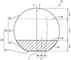
最初将描述根据本实施例的碳化硅单晶衬底的构造。如图1和图2所示,碳化硅单晶衬底10包括第一主表面11、与第一主表面11相反的第三主表面13、以及位于第一主表面11与第三主表面13之间的侧端面30。侧端面30由平面的取向平面31和弯曲的曲部32构成。取向平面31沿<11-20>方向延伸。取向平面31基本上呈矩形。取向平面31的纵向方向是<11-20>方向。垂直于取向平面31的方向可以是<1-100>方向。The configuration of the silicon carbide single crystal substrate according to the present embodiment will be initially described. As shown in FIGS. 1 and 2 , silicon carbide
如图2所示,在从垂直于第一主表面11的方向上观察时,侧端面30包括呈直线的取向平面31和呈弧形的曲部32。由曲部32上的任意三点形成的三角形的外接圆的中心可以被定义为第一主表面11的中心5。碳化硅单晶衬底10(下文可以简称为“单晶衬底”)由碳化硅单晶制成。碳化硅单晶的多型例如是4H-SiC。与其他多型相比,4H-SiC的电子迁移率和介电强度更高。碳化硅单晶衬底10包含诸如氮(N)的n型杂质。碳化硅单晶衬底10例如具有n型导电类型。As shown in FIG. 2 , when viewed from a direction perpendicular to the first
第一主表面11例如是{0001}平面或者从{0001}平面倾斜至多8°的表面。当第一主表面11从{0001}平面倾斜时,第一主表面11的法线的倾斜的方向(偏离方向)例如是<11-20>方向。从{0001}平面的倾斜的角(偏离角)可以不小于1°或不小于2°。偏离角可以不大于7°或不大于6°。第一主表面11具有例如不小于100mm的最大直径(直径)。最大直径可以不小于150mm、不小于200mm、或不小于250mm。最大直径的上限不被特别地限制。最大直径的上限可以例如被设定为300mm。当第一主表面11位于(0001)平面侧时,第三主表面13位于(000-1)平面侧。反之,当第一主表面11位于(000-1)平面侧时,第三主表面13位于(0001)平面侧。第一主表面11包括从第一主表面11的外周105朝向中心5延伸至多5mm的端部区域103(第一端部区域)以及由端部区域103围绕的中央区域104。端部区域103与取向平面31连续。The first
现将描述端部区域的翘曲量。The warpage amount of the end region will now be described.
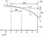
图3示出在垂直于第一主表面11的方向上观察时,此刻观察到将取向平面31垂直地分成两个相等区段的截面时的第一主表面11的横截面轮廓15。在图3中,纵坐标表示第一主表面11的相对高度,横坐标表示第一主表面上的在垂直于取向平面31的方向上的位置。稍后将描述测量相对高度的方法。第一位置1是指当在垂直于第一主表面11的方向上观察时取向平面的中心中的位置。第二位置2是指当在第一主表面11的中心5观察时曲部32的与第一位置1相反的位置。如图3所示,在截面图中,朝向取向平面31,端部区域103可以在背离与第一主表面11相反的第三主表面13的方向上向上翘曲。第一主表面11的相对高度可以在第二位置2处最低。第一主表面11的相对高度可以从第二位置2朝向第一位置1逐渐增大。FIG. 3 shows the
图4是图3中区域IV的放大图。在图4中,横坐标表示在垂直于取向平面31的方向上与取向平面31的距离。横坐标上的位置0是指取向平面31的位置。假设最小二乘线4,其由从与取向平面31相距3mm的位置朝向第一主表面11的中心5延伸至与从该定相平面相距5mm的位置的区域102中的第一主表面11的横截面轮廓15算出。翘曲量101表示其中最小二乘线4与取向平面31相交的点6和取向平面31与第一主表面11之间的接触点7之间的距离。接触点7可以在垂直于第一主表面11的方向上位于取向平面31中的最高位置。FIG. 4 is an enlarged view of area IV in FIG. 3 . In FIG. 4 , the abscissa represents the distance from the
如图5所示,在截面图中,朝向取向平面31,端部区域103可以在朝向与第一主表面11相反的第三主表面13的方向上向下翘曲。在图5中的横坐标表示在垂直于取向平面31的方向上与取向平面31的距离。横坐标上的位置0是指取向平面31的位置。假设最小二乘线4,其由从与取向平面31相距3mm的位置朝向第一主表面11的中心5延伸至与该定相平面相距5mm的位置的区域102中的第一主表面11的横截面轮廓15算出。翘曲量101表示其中最小二乘线4与沿取向平面31延伸的虚拟面36相交的点8和取向平面31与第一主表面11之间的接触点7之间的距离。接触点7可以是在垂直于第一主表面11的方向上位于取向平面31中的最低位置。As shown in FIG. 5 , in cross-sectional view, towards the
如上所述,朝向外周105,端部区域103可以在背离碳化硅单晶衬底10的第三主表面13的方向上向上翘曲,或者反之,可以在朝向第三主表面13的方向上向下翘曲。第三主表面13包括从第三主表面13的外周延伸至多5mm的第二端部区域。第二端部区域与取向平面31连续。当第一端部区域103向上翘曲时,第二端部区域可能向下翘曲。反之,当第一端部区域103向下翘曲时,第二端部区域可能向上翘曲。在垂直于第一主表面11的方向上,第一端部区域103的翘曲量101不大于3μm。翘曲量101优选不大于2μm,并且更优选不大于1μm。类似地,在垂直于第三主表面13的方向上,第二端部区域的翘曲量101可以不大于3μm、不大于2μm或不大于1μm。As described above, toward the
现将描述一种测量翘曲量的方法。A method of measuring the amount of warpage will now be described.
例如,能够利用由Kohzu Precision Co.,Ltd.制造的Dyvoce系列表面轮廓系统来测量翘曲量。如图6所示,表面仿形系统57主要包括例如激光位移计50和XY载台55。激光位移计50主要包括光发射元件51和光接收元件52。光发射元件51例如通过半导体激光器来实现。For example, the amount of warpage can be measured using a Dyvoce series surface profile system manufactured by Kohzu Precision Co., Ltd. As shown in FIG. 6 , the
如图6所示,碳化硅单晶衬底10被布置在XY载台55上。用来自光发射元件51的入射光53照射碳化硅单晶衬底10的第一主表面11。由光接收元件52感测来自第一主表面11的反射光54。因此,能够测量激光位移计50到第一主表面11的距离。通过使XY载台55在二维平面内移动,能够测量沿第一主表面11的径向方向的表面的相对高度的轮廓。As shown in FIG. 6 , silicon carbide
垂直于第一主表面11的直线58与入射光53的入射的方向之间的角度是例如不小于0°且不大于60°。当角度大于60°时,由于特别是在第一主表面11的外周附近上的漫射而导致噪声是较高的,并且难以精确地测量碳化硅单晶衬底10的表面轮廓。在本实施例中,通过将该角度设定为较小,能够精确地测量第一主表面11的外周附近的表面轮廓(特别是,第一主表面11与侧端面30之间的切线7附近的轮廓)。The angle between the straight line 58 perpendicular to the first
例如,沿着图2中的线段3测量第一主表面11的相对高度。然后,使用XY载台55,将碳化硅单晶衬底10例如沿<11-20>方向上移位10mm。然后,沿平行于线段3的线段测量第一主表面11的相对高度。如上所述,以10mm间隔测量第一主表面11的相对高度曲线。For example, the relative height of the first
当在垂直于第一主表面11的方向上观察时,与取向平面31连续的端部区域103的翘曲量101不大于3μm意旨,当在取向平面31的延伸方向(即,<11-20>方向)上以10mm间隔在测量位置处测量端部区域103的翘曲量101时,所有测量位置处的端部区域103的翘曲量101不大于3μm。When viewed in the direction perpendicular to the first
(碳化硅外延衬底)(Silicon carbide epitaxial substrate)
现将描述根据本实施例的碳化硅外延衬底的构造。如图7所示,碳化硅外延衬底100包括碳化硅单晶衬底10和碳化硅层20。碳化硅层20位于第一主表面11上。碳化硅层20包括与第一主表面11接触的第四主表面14以及与第四主表面14相反的第二主表面12。第二主表面12不带有从取向平面31在<1-100>方向上延伸并且长度不短于1mm的堆垛层错。第二主表面优选地不带有长度不短于1.5mm的堆垛层错,并且更优选不带有长度不短于2mm的堆垛层错。堆垛层错的长度被定义为在<1-100>方向上的长度。第二主表面12可以包括从与取向平面31不同的区域延伸的堆垛层错、在与<1-100>方向不同的方向上延伸的堆垛层错、或者具有短于1mm的长度的堆垛层错。The configuration of the silicon carbide epitaxial substrate according to the present embodiment will now be described. As shown in FIG. 7 , the silicon
碳化硅层20是通过外延生长形成的外延层。碳化硅层20包含诸如氮的n型杂质。碳化硅层20中包含的n型杂质的浓度可以低于碳化硅单晶衬底10中包含的n型杂质的浓度。碳化硅层20限定第二主表面12。碳化硅层20可以具有例如不小于5μm、不小于10μm或不小于15μm的厚度。The
(观察堆垛层错的方法)(How to observe stacking faults)
现将描述一种观察堆垛层错的方法。例如,使用由Photon Design Corporation制造的光致发光成像设备用于观察堆垛层错。当用激发光照射碳化硅外延衬底100的第二主表面12时,在第二主表面12中观察到光致发光。例如,采用白光作为激发光。白光例如穿过313nm带通滤波器并且发射到第二主表面12。光致发光例如穿过740nm低通滤波器并于此后到达诸如相机的光接收元件。如上所述,拍摄第二主表面12上的测量区域的光致发光图像。A method of observing stacking faults will now be described. For example, a photoluminescence imaging apparatus manufactured by Photon Design Corporation is used for observing stacking faults. When second
例如,通过在使碳化硅外延衬底100在平行于第二主表面12的方向上移动的同时来拍摄第二主表面12的光致发光图像,映射整个第二主表面12上的光致发光图像。在光致发光图像中,从取向平面31呈线性伸的白色条纹被识别为堆垛层错。For example, by taking a photoluminescence image of the second
(碳化硅单晶衬底的第一变型)(First modification of silicon carbide single crystal substrate)
如图8所示,假设一个示例,当在垂直于第一主表面11的方向上观察时,将取向平面31垂直地分成两个相等区段的线段3在碳化硅单晶衬底10中分成四个相等区段。第一主表面11包括从取向平面31延伸到与线段3的1/4相对应的位置44的下部区域41。线段3位于第一主表面11上。线段3穿过第一主表面11的中心5。位置44定义与线段3垂直的线段。当线段3分成四个相等区段时,位置44位于与第一位置1相距对应于线段3的1/4长度的位置处,该第一位置表示线段3与取向平面31之间的接触点。As shown in FIG. 8 , assuming an example, when viewed in a direction perpendicular to first
当在垂直于第一主表面11的方向观察时,呈弧形的曲部32包括下弧部33、中央弧部34和上弧部35。中央弧部34位于下弧部33与上弧部35之间。下弧部33由下部区域41限定。与下部区域41的端部33连续的端部区域103的翘曲量101不大于3μm。当在垂直于第一主表面11的方向上观察时,端部区域103的翘曲量101不大于3μm意旨,当在沿端部33的方向上以10mm间隔在多个测量位置处测量端部区域103的翘曲量101时,所有测量位置处的端部区域103的翘曲量101不大于3μm。端部区域103的翘曲量101优选不大于2μm,更优选不大于1μm。The
(碳化硅外延衬底的第一变型)(First Variation of Silicon Carbide Epitaxial Substrate)
如图7所示,根据第一变型的碳化硅外延衬底100包括根据第一变型的碳化硅单晶衬底10以及碳化硅层20。碳化硅层20位于第一主表面11上。碳化硅层20包括与第一主表面11接触的第四主表面14以及与第四主表面14相反的第二主表面12。第二主表面12不带有从下部区域41的端部33在<1-100>方向上延伸并且长度不短于1mm的堆垛层错。第二主表面12可以包括从与下部区域41的端部33不同的区域延伸的堆垛层错、在与<1-100>方向不同的方向上延伸的堆垛层错、或者具有短于1mm长度的堆垛层错。As shown in FIG. 7 , the silicon
(碳化硅单晶衬底的第二变型)(Second modification of silicon carbide single crystal substrate)
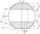
如图9所示,假设一个示例,当在垂直于第一主表面11的方向上观察时,将取向平面31垂直分成两个相等区段的线段3在根据第二变型的碳化硅单晶衬底10中分成四个相等区段。第一主表面11包括从与取向平面31相反的端部35延伸到与线段的1/4相对应的位置45的上部区域43。线段3位于第一主表面11上。线段3穿过第一主表面11的中心5。位置45定义与线段3垂直的线段。当将线段3分成四个相等区段时,位置45位于与第二位置2相距与线段3的1/4长度相对应的位置处,该第二位置2表示线段3与端部35之间的接触点。As shown in FIG. 9 , assuming an example, when viewed in a direction perpendicular to the first
当在垂直于第一主表面11的方向观察时,呈弧形的曲部32包括下弧部33、中央弧部34、和上弧部35。中央弧部34位于下弧部33与上弧部35之间。上弧部35由上部区域43限定。与上部区域43的端部35连续的端部区域103的翘曲量101不大于3μm。当在垂直于第一主表面11的方向上观察时,与上部区域43的端部35连续的端部区域103的翘曲量101不大于3μm意旨,当在沿端部35的方向上以10mm间隔在测量位置处测量端部区域103的翘曲量101时,所有测量位置处的端部区域103的翘曲量101不大于3μm。端部区域103的翘曲量101优选不大于2μm,更优选不大于1μm。The
(碳化硅外延衬底的第二变型)(Second modification of silicon carbide epitaxial substrate)
如图7所示,根据第二变型的碳化硅外延衬底100包括根据第二变型的碳化硅单晶衬底10以及碳化硅层20。碳化硅层20位于第一主表面11上。碳化硅层20包括与接触第一主表面11的表面14相反的第二主表面12。第二主表面12不带有从上部区域43的端部35沿<1-100>方向上延伸并且长度不短于1mm的堆垛层错。第二主表面12可以包括从与上部区域43的端部35不同的区域延伸的堆垛层错、在与<1-100>方向不同的方向延伸的堆垛层错、或者具有短于1mm长度的堆垛层错。As shown in FIG. 7 , a silicon
(碳化硅单晶衬底的第三变型)(Third modification of silicon carbide single crystal substrate)
如图10所示,假设一个示例,当在垂直于第一主表面11的方向上观察时,将取向平面31垂直分成两个相等区段的线段3在根据第三变型的碳化硅单晶衬底10中分成四个相等区段。第一主表面11包括从取向平面31延伸到与线段的1/4相对应的位置44的下部区域41以及从与取向平面31相反的端部35延伸到与线段的1/4相对应的位置45的上部区域43。线段3位于第一主表面11上。线段3穿过第一主表面11的中心5。位置44定义与线段3垂直的线段。当将线段3分成四个相等区段时,位置44位于与第一位置1相距对应于线段3的1/4长度的位置处,该第一位置1表示线段3与取向平面31之间的接触点。当将线段3分成四个相等区段时,位置45位于与第二位置2相距对应于线段3的1/4长度的位置处,该第二位置2表示线段3与端部35之间的接触点。As shown in FIG. 10 , assuming an example, when viewed in the direction perpendicular to the first
当在垂直于第一主表面11的方向上观察时,呈弧形的曲部32包括下弧部33、中央弧部34、和上弧部35。中央弧部34位于下弧部33与上弧部35之间。上弧部35由上部区域43限定。下弧部33由下部区域41限定。The
与下部区域41的端部33连续的端部区域103的翘曲量101不大于3μm。当在垂直于第一主表面11的方向上观察时,与下部区域41的端部33连续的端部区域103的翘曲量101不大于3μm意旨,当在沿端部33的方向上以10mm间隔在测量位置处测量端部区域103的翘曲量101时,所有测量位置处的端部区域103的翘曲量101不大于3μm。端部区域103的翘曲量101优选不大于2μm,更优选不大于1μm。The
与上部区域43的端部35连续的端部区域103的翘曲量101不大于3μm。当在垂直于第一主表面11的方向观察时,与上部区域43的端部35连续的端部区域103的翘曲量101不大于3μm意旨,当在沿端部35的方向上以10mm间隔在测量位置处测量端部区域103的翘曲量101时,所有测量位置处的端部区域103的翘曲量101不大于3μm。端部区域103的翘曲量101优选不大于2μm,更优选不大于1μm。The
(碳化硅外延衬底的第三变型)(Third modification of silicon carbide epitaxial substrate)
如图7所示,根据第三变型的碳化硅外延衬底100包括根据第三变型所述的碳化硅单晶衬底10以及碳化硅层20。碳化硅层20位于第一主表面11上。碳化硅层20包括与接触第一主表面11的表面14相反的第二主表面12。第二主表面12不带有从下部区域41的端部33沿<1-100>方向延伸并且长度不短于1mm的堆垛层错,并且不带有从上部区域43的端部35在<1-100>方向上延伸并且长度不短于1mm的堆垛层错。第二主表面12可以包括从与上部区域43的端部35和下部区域41的端部33不同的区域延伸的堆垛层错、在与<1-100>方向不同的方向上延伸的堆垛层错、或者具有短于1mm长度的堆垛层错。As shown in FIG. 7 , the silicon
(制造碳化硅单晶衬底的方法)(Method of Manufacturing Silicon Carbide Single Crystal Substrate)
现将描述根据本实施例的制造碳化硅单晶衬底的方法。A method of manufacturing a silicon carbide single crystal substrate according to the present embodiment will now be described.
例如利用升华法制造多型4H的碳化硅单晶锭80。如图11所示,碳化硅单晶锭80包括上表面81、下表面82、和侧表面83。侧表面83位于上表面81与下表面82之间。侧表面83被连续设置到上表面81并且被连续设置到下表面82。上表面81例如呈凸状弯曲。下表面82例如基本上呈平面并且基本上呈圆形。在截面图中,侧表面83具有从下表面82朝上表面81增加的宽度。当使用坩埚以升华法制造碳化硅单晶时,上表面81面向碳化硅源材料,并且下表面82面向晶种衬底。For example, a polytype 4H silicon carbide
然后,成形碳化硅单晶锭80。具体地,准备第一磨石61和第二磨石62。第一磨石61被布置成面向侧表面83。第二磨石62被布置成面向上表面81。碳化硅单晶锭80的下表面82被固定到支架65。支架65例如由不锈钢制成。通过使支架65围绕旋转轴67旋转,使固定到支架65的碳化硅单晶锭80旋转。随着将第一磨石61压靠在碳化硅单晶锭80的侧表面83上,同时使碳化硅单晶锭80旋转,研磨侧表面83。类似地,随着将第二磨石62压靠在碳化硅单晶锭80的上表面81上,同时使碳化硅单晶锭80旋转,研磨上表面81。因此,碳化硅单晶锭80被成形成大致呈柱状的形状(参见图13)。碳化硅单晶锭80具有大致呈圆形的上表面81、大致呈圆形的下表面82和大致呈圆柱形的侧表面83。支架65从碳化硅单晶锭80的下表面82移开。Then, the silicon carbide
然后,将支架71附接到碳化硅单晶锭80的下表面82。当碳化硅单晶锭80被静止固定到支架71时,第三磨石68被压靠在碳化硅单晶锭80的侧表面83上。随着在用箭头所示的方向70上压靠第三磨石68,同时其沿平行于侧表面83的方向69进行往复运动,研磨侧表面83。因此,在碳化硅单晶锭80中形成取向平面84(参见图15)。侧表面83由平面的取向平面84和曲面部85限定。取向平面84基本上呈矩形。Then, the
然后,将保护部92附接到取向平面84。设置保护部92以覆盖整个平面的取向平面84(见图16)。保护部92例如用粘合剂固定到取向平面84。虽然保护部92的形状不受特别限制,但其例如呈板状。例如,采用碳化硅作为保护部92的材料。保护部92可以由单晶碳化硅或多晶碳化硅构成。呈板状的保护部92具有不小于10mm的厚度。Then, the
如图16所示,碳化硅单晶锭80被保持在基座91上,而取向平面84用保护部92覆盖。基座91的表面96被设置有呈弧形的凹部95。碳化硅单晶锭80的侧表面83的曲面部85被布置在凹部95中。碳化硅单晶锭80例如用粘合剂固定到基座91。碳化硅单晶锭80的取向平面84相对于基座91的表面96倾斜。保护部92可以远离表面96。As shown in FIG. 16 , the silicon carbide
然后,切割碳化硅单晶锭80。如图17所示,当从碳化硅单晶锭80观察时,线锯93被布置在基座91的相反侧。随着底座91在用箭头所示的方向94上移动,同时线锯93摆动,用线锯93切割碳化硅单晶锭80。多个线锯93可以在垂直于上表面81的方向上对齐。线锯93在与碳化硅单晶锭80接触之前与保护部92接触。在切开保护部92的一部分之后,线锯93开始切割碳化硅单晶锭80。Then, the silicon carbide
在用线锯93切割碳化硅单晶锭80时,理想地,线锯93大致垂直地引入到碳化硅单晶锭80的侧表面83中。然而,在开始切割时,线锯93到碳化硅单晶锭80的侧表面83中的引入的角度并不稳定,并且线锯93可能倾斜地被引入到侧表面83中。当在不需要使用保护部92就开始用线锯93切割碳化硅单晶锭80时,线锯93趋于倾斜地引入到侧表面83。When the silicon carbide
在本实施例中,保护部92覆盖取向平面84的整个表面。尽管首先切割的保护部92的切割面可能相对于保护部92的侧表面弯曲,但切割面将逐渐基本上垂直于侧表面。因而,继保护部92之后切割的碳化硅单晶锭80被切割为基本上垂直于碳化硅单晶锭80的侧表面83。因此,能够减小与定位平面31连续的端部区域103的翘曲量101(参见图4)。如上所述,制备碳化硅单晶衬底10(参见图1)。In the present embodiment, the
(制造碳化硅外延衬底的方法)(Method of Manufacturing Silicon Carbide Epitaxial Substrate)
现将描述一种制造碳化硅外延衬底的方法。例如,通过热壁化学气相沉积(CVD),通过外延生长在碳化硅单晶衬底10上形成碳化硅层20。具体地,将碳化硅单晶衬底10布置在CVD反应室内。例如,在反应室内的压力从大气压降到约1×10⁻⁶Pa之后,开始碳化硅单晶衬底10的温升。在温升期间,将代表载气的氢(H2)气引入到反应室中。A method of fabricating a silicon carbide epitaxial substrate will now be described. The
在反应室中的温度例如达到约1600℃之后,将源气体和掺杂气体引入到反应室内。源气体包括Si源气体和C源气体。例如,能够使用硅烷(SiH4)气作为Si源气体。例如,能够使用丙烷(C3H8)气作为C源气体。硅烷气和丙烷气的流量例如分别设定为46sccm和14sccm。硅烷气与氢气的体积比例如设定为0.04%。源气体的C/Si比例如设定为0.9。After the temperature in the reaction chamber reaches, for example, about 1600° C., the source gas and the dopant gas are introduced into the reaction chamber. The source gas includes Si source gas and C source gas. For example, silane (SiH4 ) gas can be used as the Si source gas. For example, propane (C3 H8 ) gas can be used as the C source gas. The flow rates of the silane gas and the propane gas are set to, for example, 46 sccm and 14 sccm, respectively. The volume ratio of silane gas and hydrogen gas is set to, for example, 0.04%. The C/Si ratio of the source gas is set to, for example, 0.9.
例如,使用氨(NH3)气作为掺杂气体。氨气比具有三键的氮气更容易热分解。通过使用氨气,能够预期载体浓度的平面内均匀性的提高。氨气相对于氢气的浓度例如设定为1ppm。通过将载气体、源气体、和掺杂气体引入到反应室中,同时将碳化硅单晶衬底10加热到约1600℃,通过外延生长在碳化硅单晶衬底10上形成碳化硅层20(参见图7和图18)。因此,制成包括碳化硅单晶衬底10和碳化硅层20的碳化硅外延衬底100。For example, ammonia (NH3 ) gas is used as the dopant gas. Ammonia is easier to thermally decompose than nitrogen with triple bonds. By using ammonia gas, an improvement in the in-plane uniformity of the carrier concentration can be expected. The concentration of the ammonia gas relative to the hydrogen gas is set to, for example, 1 ppm.
(制造碳化硅半导体器件的方法)(Method of Manufacturing Silicon Carbide Semiconductor Device)
现将描述根据本实施例的制造碳化硅半导体器件300的方法。A method of manufacturing the silicon
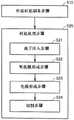
根据本实施例的制造碳化硅半导体器件的方法主要包括外延衬底制备步骤(图19:S10)和衬底处理步骤(图19:S20)。The method of manufacturing a silicon carbide semiconductor device according to the present embodiment mainly includes an epitaxial substrate preparation step ( FIG. 19 : S10 ) and a substrate processing step ( FIG. 19 : S20 ).
起初,执行外延衬底制备步骤(图19:S10)。具体地,利用前述的制造碳化硅外延衬底的方法,制备碳化硅外延衬底100(参见图7和图18)。Initially, an epitaxial substrate preparation step is performed (FIG. 19: S10). Specifically, using the aforementioned method of manufacturing a silicon carbide epitaxial substrate, a silicon
然后,执行衬底处理步骤(图19:S20)。具体地,通过处理碳化硅外延衬底来制造碳化硅半导体器件。“处理”包括各种类型的处理,诸如离子注入、热处理、蚀刻、氧化膜的形成、电极的形成、和切割(dicing)。衬底处理步骤可以至少包括离子注入、热处理、蚀刻、氧化膜的形成、电极的形成和切割中的任何处理。Then, a substrate processing step is performed (FIG. 19: S20). Specifically, silicon carbide semiconductor devices are fabricated by processing silicon carbide epitaxial substrates. "Processing" includes various types of processes such as ion implantation, heat treatment, etching, formation of oxide films, formation of electrodes, and dicing. The substrate processing step may include at least any of ion implantation, heat treatment, etching, formation of oxide films, formation of electrodes, and dicing.
下面将描述制造代表碳化硅半导体器件的一个示例的金属氧化物半导体场效应晶体管(MOSFET)的方法。衬底处理步骤(图19:S20包括离子注入步骤(图19:S21)、氧化膜形成步骤(图19:S22)、电极形成步骤(图19:S23)和切割步骤(图19:S24)。A method of manufacturing a metal oxide semiconductor field effect transistor (MOSFET) representing one example of a silicon carbide semiconductor device will be described below. The substrate processing step ( FIG. 19 : S20 ) includes an ion implantation step ( FIG. 19 : S21 ), an oxide film forming step ( FIG. 19 : S22 ), an electrode forming step ( FIG. 19 : S23 ), and a cutting step ( FIG. 19 : S24 ).
首先,执行离子注入步骤(图19:S21)。将诸如铝(Al)的p型杂质注入到第二主表面12中,其中形成设置有开口的掩模(未示出)。因此,形成具有p型导电类型的体区132。然后,将诸如磷(P)的n型杂质注入到体区132中的规定位置中。因此,形成具有n型导电类型的源区133。然后,将诸如铝的p型杂质注入到源区133中的规定位置。因此,形成具有p型导电类型的接触区134(参见图20)。First, an ion implantation step is performed (FIG. 19: S21). A p-type impurity such as aluminum (Al) is implanted into the second
碳化硅层20中除体区132、源区133、和接触区134之外的部分是漂移区131。源区133通过体区132与漂移区131间隔开。通过将碳化硅外延衬底100加热到大约不低于300℃且不高于600℃的温度,可以注入离子。在离子注入之后,碳化硅外延衬底100经受活化退火。注入在碳化硅层20中的杂质通过激活退火而活化,从而在每个区域中产生载体。用于活化退火的气氛可以例如是氩(Ar)气氛。活化退火的温度可以例如设定为约1800℃。活化退火的时间段可以例如设定为约30分钟。A portion of the
然后,执行氧化膜形成步骤(图19:S22)。例如,随着在含氧气氛中加热碳化硅外延衬底100,在第二主表面12上形成氧化膜136(参见图21)。氧化膜136例如由二氧化硅(SiO2)构成。氧化膜136充当栅极绝缘膜。用于热氧化处理的温度可以例如设定为约1300℃。热氧化处理的时间可以例如设定为约30分钟。Then, an oxide film forming step is performed (FIG. 19: S22). For example, as silicon
在形成氧化膜136之后,可以在氮气氛中进一步执行热处理。例如,可以在一氧化氮(NO)或一氧化二氮(N2O)气氛中在约1100℃下进行热处理约达一小时。此后,可以在氩气氛中进一步进行热处理。例如,可以在约1100℃至1500℃的温度下在氩气氛中进行热处理约达1小时。After the
然后,执行电极形成步骤(图19:S23)。在氧化膜136上形成第一电极141。第一电极141充当栅电极。例如,用CVD形成第一电极141。第一电极141例如由通过含有杂质而导电的多晶硅构成。在面向源区133和体区132的位置处形成第一电极141。Then, an electrode forming step is performed (FIG. 19: S23). The
然后,形成覆盖第一电极141的层间绝缘膜137。例如,用CVD形成层间绝缘膜137。层间绝缘膜137例如由二氧化硅构成。层间绝缘膜137被形成为与第一电极141和氧化膜136接触。然后,蚀刻掉规定位置处的氧化膜136和层间绝缘膜137。因此,透过氧化膜136暴露源区133和接触区134。Then, the
例如,利用溅射在该暴露部分中形成第二电极142。第二电极142充当源电极。第二电极142例如由钛、铝、和硅构成。在形成第二电极142之后,在例如约900℃至1100℃的温度下加热第二电极142和碳化硅外延衬底100。因此,使第二电极142与碳化硅外延衬底100彼此呈欧姆接触。然后,互连层138被形成为与第二电极142接触。互连层138由例如含有铝的材料构成。For example, the
然后,在第三主表面13上形成第三电极143。第三电极143充当漏电极。第三电极143例如由含有镍和硅的合金(例如,NiSi)构成。Then, the
然后,执行切割步骤(图19:S24)。例如,随着沿切割线切割碳化硅外延衬底100,碳化硅外延衬底100被分成多个半导体芯片。如上所述,制成碳化硅半导体器件300(参见图22)。Then, the cutting step is performed (FIG. 19: S24). For example, as the silicon
尽管上文参照MOSFET描述了根据本公开的制造碳化硅半导体器件的方法,但根据本公开的制造方法不限于此。根据本公开的制造方法可应用于各种碳化硅半导体器件,诸如绝缘栅双极晶体管(IGBT)、肖特基势垒二极管(SBD)、晶闸管、门极可关断晶闸管(GTO)和PiN二极管。Although the method of manufacturing the silicon carbide semiconductor device according to the present disclosure is described above with reference to the MOSFET, the manufacturing method according to the present disclosure is not limited thereto. The fabrication method according to the present disclosure can be applied to various silicon carbide semiconductor devices, such as insulated gate bipolar transistors (IGBTs), Schottky barrier diodes (SBDs), thyristors, gate turn-off thyristors (GTOs), and PiN diodes .
应当理解,本文公开的实施例在各方面皆是说明性而非限制性。本发明的范围由权利要求的术语限定,而非由上述实施例限定,并且旨在包括在与权利要求的用语等价的范围和含义内的任何修改。It should be understood that the embodiments disclosed herein are illustrative and non-restrictive in every respect. The scope of the present invention is defined by the terms of the claims, rather than the above-described embodiments, and is intended to include any modifications within the scope and meaning equivalent to the terms of the claims.
附图标记列表List of reference signs
1第一位置;2第二位置;3线段;4最小二乘线;5中心;6,8点;7,9接触点、切线;10单晶衬底;11第一主表面;12第二主表面;13第三主表面(表面);14第四主表面(表面);15横截面轮廓;20碳化硅层;30侧端面;31,84取向平面;32曲部;33下弧部(端部);34中央弧部;35上弧部(端部);36虚拟表面;41下部区域;43上部区域;50激光位移计;51光发射元件;52光接收元件;53入射光;54反射光;55载台;57表面仿形系统;61第一磨石;62第二磨石;65,71支架;67旋转轴;68第三磨石;80单晶锭;81上表面;82下表面;83侧表面;85曲面部;91基座;92保护部;93线锯;95凹部;96表面;100碳化硅外延衬底;101翘曲量;102区域;103端部区域(第一端部区域);104中央区;105外周;131漂移区;132体区;133源区;134接触区;136氧化膜;137层间绝缘膜;138互连层;141第一电极;142第二电极;143第三电极;300碳化硅半导体器件。1 first position; 2 second position; 3 line segment; 4 least squares line; 5 center; 6, 8 points; 7, 9 contact points, tangents; 10 single crystal substrate; main surface; 13 third main surface (surface); 14 fourth main surface (surface); 15 cross-sectional profile; 20 silicon carbide layer; 30 side end face; 31,84 orientation plane; 32 curved part; end); 34 central arc; 35 upper arc (end); 36 virtual surface; 41 lower area; 43 upper area; 50 laser displacement gauge; 51 light emitting element; 52 light receiving element; 53 incident light; 54 Reflected Light; 55 Stage; 57 Surface Profiling System; 61 First Grinding Stone; 62 Second Grinding Stone; lower surface; 83 side surface; 85 curved surface part; 91 base; 92 protection part; 93 wire saw; 95 recessed part; 96 surface; 100 silicon carbide epitaxial substrate; 101 warpage amount; 104 central region; 105 periphery; 131 drift region; 132 body region; 133 source region; 134 contact region; 136 oxide film; 137 interlayer insulating film; 138 interconnection layer; 141 first electrode; 142 Second electrode; 143 third electrode; 300 silicon carbide semiconductor device.
Claims (17)
Applications Claiming Priority (3)
| Application Number | Priority Date | Filing Date | Title |
|---|---|---|---|
| JP2015-228517 | 2015-11-24 | ||
| JP2015228517 | 2015-11-24 | ||
| PCT/JP2016/072775WO2017090279A1 (en) | 2015-11-24 | 2016-08-03 | Silicon carbide single crystal substrate, silicon carbide epitaxial substrate, and method for manufacturing silicon carbide semiconductor device |
Publications (2)
| Publication Number | Publication Date |
|---|---|
| CN108369893A CN108369893A (en) | 2018-08-03 |
| CN108369893Btrue CN108369893B (en) | 2022-07-19 |
Family
ID=58763336
Family Applications (1)
| Application Number | Title | Priority Date | Filing Date |
|---|---|---|---|
| CN201680068455.4AActiveCN108369893B (en) | 2015-11-24 | 2016-08-03 | Silicon carbide single crystal substrate, silicon carbide epitaxial substrate and method for manufacturing silicon carbide semiconductor device |
Country Status (4)
| Country | Link |
|---|---|
| US (3) | US10283596B2 (en) |
| CN (1) | CN108369893B (en) |
| DE (1) | DE112016005373T5 (en) |
| WO (1) | WO2017090279A1 (en) |
Families Citing this family (5)
| Publication number | Priority date | Publication date | Assignee | Title |
|---|---|---|---|---|
| JP6597381B2 (en)* | 2016-02-22 | 2019-10-30 | 住友電気工業株式会社 | Method for manufacturing silicon carbide substrate, method for manufacturing silicon carbide epitaxial substrate, and method for manufacturing silicon carbide semiconductor device |
| JP7310805B2 (en)* | 2018-05-09 | 2023-07-19 | 住友電気工業株式会社 | Silicon carbide epitaxial substrate and method for manufacturing silicon carbide semiconductor device |
| JP6585799B1 (en) | 2018-10-15 | 2019-10-02 | 昭和電工株式会社 | Method for evaluating SiC substrate and method for producing SiC epitaxial wafer |
| JPWO2022004181A1 (en)* | 2020-07-02 | 2022-01-06 | ||
| JP7695902B2 (en)* | 2022-01-27 | 2025-06-19 | 住友重機械工業株式会社 | Wafer Processing Equipment |
Family Cites Families (20)
| Publication number | Priority date | Publication date | Assignee | Title |
|---|---|---|---|---|
| JP2003327497A (en)* | 2002-05-13 | 2003-11-19 | Sumitomo Electric Ind Ltd | GaN single crystal substrate, nitride-based semiconductor epitaxial substrate, nitride-based semiconductor device, and method of manufacturing the same |
| US7422634B2 (en)* | 2005-04-07 | 2008-09-09 | Cree, Inc. | Three inch silicon carbide wafer with low warp, bow, and TTV |
| JP2007301688A (en) | 2006-05-12 | 2007-11-22 | Naoetsu Electronics Co Ltd | Workpiece cutting method |
| JP2010098253A (en)* | 2008-10-20 | 2010-04-30 | Sumitomo Electric Ind Ltd | Semiconductor substrate, method of manufacturing the same, and method of manufacturing semiconductor device |
| WO2011046021A1 (en)* | 2009-10-13 | 2011-04-21 | 住友電気工業株式会社 | Silicon carbide substrate manufacturing method and silicon carbide substrate |
| EP2597670B1 (en) | 2010-03-31 | 2016-03-30 | EV Group E. Thallner GmbH | Method for permanently connecting two metal surfaces |
| JP2011243770A (en)* | 2010-05-19 | 2011-12-01 | Sumitomo Electric Ind Ltd | Silicon carbide substrate, semiconductor device, and silicon carbide substrate manufacturing method |
| JP2012038973A (en)* | 2010-08-09 | 2012-02-23 | Siltronic Ag | Silicon wafer and method of producing the same |
| US8890170B2 (en)* | 2010-11-15 | 2014-11-18 | Hoya Corporation | Silicon carbide substrate, semiconductor device and method for manufacturing silicon carbide substrate |
| JP2012201543A (en)* | 2011-03-25 | 2012-10-22 | Sumitomo Electric Ind Ltd | Silicon carbide substrate |
| JP2013008769A (en)* | 2011-06-23 | 2013-01-10 | Sumitomo Electric Ind Ltd | Production method of silicon carbide substrate |
| CN103636179B (en)* | 2011-07-07 | 2017-07-07 | 瑞典爱立信有限公司 | For the method and apparatus of the Media Stream marshalling in multimedia communication network |
| US9041010B2 (en)* | 2012-05-29 | 2015-05-26 | William F. Seng | Wide band gap semiconductor wafers grown and processed in a microgravity environment and method of production |
| JP2013258243A (en)* | 2012-06-12 | 2013-12-26 | Sumitomo Electric Ind Ltd | Manufacturing method and manufacturing device of compound semiconductor substrate |
| JP6131605B2 (en)* | 2013-01-21 | 2017-05-24 | 住友電気工業株式会社 | Method for manufacturing silicon carbide semiconductor device |
| JP2014170891A (en) | 2013-03-05 | 2014-09-18 | Sumitomo Electric Ind Ltd | Silicon carbide substrate, silicon carbide substrate manufacturing method and silicon carbide semiconductor device manufacturing method |
| JP6197461B2 (en)* | 2013-08-06 | 2017-09-20 | 住友電気工業株式会社 | Silicon carbide semiconductor substrate, method of manufacturing the same, and method of manufacturing silicon carbide semiconductor device |
| JP6230112B2 (en)* | 2014-01-17 | 2017-11-15 | 旭ダイヤモンド工業株式会社 | Wafer manufacturing method and wafer manufacturing apparatus |
| JP5839069B2 (en) | 2014-03-28 | 2016-01-06 | 住友電気工業株式会社 | Silicon carbide single crystal substrate, silicon carbide epitaxial substrate, and manufacturing method thereof |
| JP2015192006A (en)* | 2014-03-28 | 2015-11-02 | セイコーエプソン株式会社 | Semiconductor wafer, light receiving sensor manufacturing method and light receiving sensor |
- 2016
- 2016-08-03CNCN201680068455.4Apatent/CN108369893B/enactiveActive
- 2016-08-03WOPCT/JP2016/072775patent/WO2017090279A1/ennot_activeCeased
- 2016-08-03DEDE112016005373.8Tpatent/DE112016005373T5/enactivePending
- 2016-08-03USUS15/772,183patent/US10283596B2/enactiveActive
- 2019
- 2019-03-26USUS16/365,172patent/US10700169B2/enactiveActive
- 2020
- 2020-05-22USUS16/882,153patent/US10998406B2/enactiveActive
Also Published As
| Publication number | Publication date |
|---|---|
| US10998406B2 (en) | 2021-05-04 |
| DE112016005373T5 (en) | 2018-08-09 |
| CN108369893A (en) | 2018-08-03 |
| WO2017090279A1 (en) | 2017-06-01 |
| US10283596B2 (en) | 2019-05-07 |
| US20180323262A1 (en) | 2018-11-08 |
| US20190221647A1 (en) | 2019-07-18 |
| US10700169B2 (en) | 2020-06-30 |
| US20200287000A1 (en) | 2020-09-10 |
Similar Documents
| Publication | Publication Date | Title |
|---|---|---|
| CN108369893B (en) | Silicon carbide single crystal substrate, silicon carbide epitaxial substrate and method for manufacturing silicon carbide semiconductor device | |
| US10697086B2 (en) | Method for manufacturing silicon carbide epitaxial substrate, method for manufacturing silicon carbide semiconductor device, and apparatus for manufacturing silicon carbide epitaxial substrate | |
| US20190013198A1 (en) | Silicon carbide epitaxial substrate and method for manufacturing silicon carbide semiconductor device | |
| US10121865B2 (en) | Silicon carbide epitaxial substrate and method of manufacturing silicon carbide semiconductor device | |
| CN110214363A (en) | The method of silicon carbide epitaxy substrate and manufacture sic semiconductor device | |
| JP2017108179A (en) | Silicon carbide single crystal substrate, silicon carbide epitaxial substrate and silicon carbide semiconductor device manufacturing method | |
| CN110214362A (en) | The method of silicon carbide epitaxy substrate and manufacture sic semiconductor device | |
| JP7632313B2 (en) | Silicon carbide epitaxial substrate and method for manufacturing silicon carbide semiconductor device | |
| CN112074928B (en) | Silicon carbide epitaxial substrate and method for manufacturing silicon carbide semiconductor device | |
| JP6930640B2 (en) | Method for manufacturing silicon carbide single crystal substrate, silicon carbide epitaxial substrate and silicon carbide semiconductor device | |
| US20210166941A1 (en) | Method for manufacturing silicon carbide epitaxial substrate and method for manufacturing silicon carbide semiconductor device | |
| CN112470255B (en) | Silicon carbide epitaxial substrate and manufacturing method of silicon carbide semiconductor device | |
| JP6468291B2 (en) | Silicon carbide epitaxial substrate, silicon carbide epitaxial substrate manufacturing method, and silicon carbide semiconductor device manufacturing method | |
| JP6090552B1 (en) | Method for manufacturing silicon carbide epitaxial substrate, method for manufacturing silicon carbide semiconductor device, and device for manufacturing silicon carbide epitaxial substrate | |
| US10526699B2 (en) | Silicon carbide epitaxial substrate and method for manufacturing silicon carbide semiconductor device | |
| US11862684B2 (en) | Recycle wafer of silicon carbide and method for manufacturing silicon carbide semiconductor device |
Legal Events
| Date | Code | Title | Description |
|---|---|---|---|
| PB01 | Publication | ||
| SE01 | Entry into force of request for substantive examination | ||
| SE01 | Entry into force of request for substantive examination | ||
| GR01 | Patent grant | ||
| GR01 | Patent grant |