CN108352352B - Biasable rotatable electrostatic chuck - Google Patents
Biasable rotatable electrostatic chuckDownload PDFInfo
- Publication number
- CN108352352B CN108352352BCN201680062275.5ACN201680062275ACN108352352BCN 108352352 BCN108352352 BCN 108352352BCN 201680062275 ACN201680062275 ACN 201680062275ACN 108352352 BCN108352352 BCN 108352352B
- Authority
- CN
- China
- Prior art keywords
- rotatable
- electrostatic chuck
- coupled
- coupling device
- conductive plate
- Prior art date
- Legal status (The legal status is an assumption and is not a legal conclusion. Google has not performed a legal analysis and makes no representation as to the accuracy of the status listed.)
- Active
Links
- 230000008878couplingEffects0.000claimsabstractdescription55
- 238000010168coupling processMethods0.000claimsabstractdescription55
- 238000005859coupling reactionMethods0.000claimsabstractdescription55
- 239000000758substrateSubstances0.000claimsdescription38
- 229910052751metalInorganic materials0.000claimsdescription30
- 239000002184metalSubstances0.000claimsdescription30
- 239000012212insulatorSubstances0.000claimsdescription5
- 230000000284resting effectEffects0.000claimsdescription4
- 238000007667floatingMethods0.000claimsdescription3
- 230000003068static effectEffects0.000claimsdescription3
- 238000000034methodMethods0.000description15
- 238000012545processingMethods0.000description9
- 239000004020conductorSubstances0.000description8
- 238000000151depositionMethods0.000description8
- 239000012530fluidSubstances0.000description7
- 239000000463materialSubstances0.000description7
- 230000008021depositionEffects0.000description6
- 239000007789gasSubstances0.000description6
- 238000005240physical vapour depositionMethods0.000description5
- 229910052782aluminiumInorganic materials0.000description4
- XAGFODPZIPBFFR-UHFFFAOYSA-NaluminiumChemical compound[Al]XAGFODPZIPBFFR-UHFFFAOYSA-N0.000description4
- 239000000919ceramicSubstances0.000description4
- 238000012546transferMethods0.000description4
- DNIAPMSPPWPWGF-UHFFFAOYSA-NPropylene glycolChemical compoundCC(O)CODNIAPMSPPWPWGF-UHFFFAOYSA-N0.000description3
- 239000002826coolantSubstances0.000description3
- 238000005137deposition processMethods0.000description3
- 238000010438heat treatmentMethods0.000description3
- 150000002500ionsChemical class0.000description3
- ZOKXTWBITQBERF-UHFFFAOYSA-NMolybdenumChemical compound[Mo]ZOKXTWBITQBERF-UHFFFAOYSA-N0.000description2
- 229910010293ceramic materialInorganic materials0.000description2
- 238000006243chemical reactionMethods0.000description2
- 238000004891communicationMethods0.000description2
- 229910052750molybdenumInorganic materials0.000description2
- 239000011733molybdenumSubstances0.000description2
- TWNQGVIAIRXVLR-UHFFFAOYSA-Noxo(oxoalumanyloxy)alumaneChemical compoundO=[Al]O[Al]=OTWNQGVIAIRXVLR-UHFFFAOYSA-N0.000description2
- 229910052582BNInorganic materials0.000description1
- PZNSFCLAULLKQX-UHFFFAOYSA-NBoron nitrideChemical compoundN#BPZNSFCLAULLKQX-UHFFFAOYSA-N0.000description1
- GWEVSGVZZGPLCZ-UHFFFAOYSA-NTitan oxideChemical compoundO=[Ti]=OGWEVSGVZZGPLCZ-UHFFFAOYSA-N0.000description1
- RTAQQCXQSZGOHL-UHFFFAOYSA-NTitaniumChemical compound[Ti]RTAQQCXQSZGOHL-UHFFFAOYSA-N0.000description1
- 238000010521absorption reactionMethods0.000description1
- PMHQVHHXPFUNSP-UHFFFAOYSA-Mcopper(1+);methylsulfanylmethane;bromideChemical compoundBr[Cu].CSCPMHQVHHXPFUNSP-UHFFFAOYSA-M0.000description1
- 239000003989dielectric materialSubstances0.000description1
- 238000009826distributionMethods0.000description1
- 239000010408filmSubstances0.000description1
- 229910052736halogenInorganic materials0.000description1
- 150000002367halogensChemical class0.000description1
- 239000013529heat transfer fluidSubstances0.000description1
- 238000004519manufacturing processMethods0.000description1
- 229910001092metal group alloyInorganic materials0.000description1
- 238000004377microelectronicMethods0.000description1
- 238000012544monitoring processMethods0.000description1
- 230000005855radiationEffects0.000description1
- 238000007789sealingMethods0.000description1
- 239000004065semiconductorSubstances0.000description1
- 238000009987spinningMethods0.000description1
- 239000010409thin filmSubstances0.000description1
- 239000010936titaniumSubstances0.000description1
- 229910052719titaniumInorganic materials0.000description1
- OGIDPMRJRNCKJF-UHFFFAOYSA-Ntitanium oxideInorganic materials[Ti]=OOGIDPMRJRNCKJF-UHFFFAOYSA-N0.000description1
- XLYOFNOQVPJJNP-UHFFFAOYSA-NwaterSubstancesOXLYOFNOQVPJJNP-UHFFFAOYSA-N0.000description1
Images


Classifications
- H—ELECTRICITY
- H01—ELECTRIC ELEMENTS
- H01L—SEMICONDUCTOR DEVICES NOT COVERED BY CLASS H10
- H01L21/00—Processes or apparatus adapted for the manufacture or treatment of semiconductor or solid state devices or of parts thereof
- H01L21/67—Apparatus specially adapted for handling semiconductor or electric solid state devices during manufacture or treatment thereof; Apparatus specially adapted for handling wafers during manufacture or treatment of semiconductor or electric solid state devices or components ; Apparatus not specifically provided for elsewhere
- H01L21/683—Apparatus specially adapted for handling semiconductor or electric solid state devices during manufacture or treatment thereof; Apparatus specially adapted for handling wafers during manufacture or treatment of semiconductor or electric solid state devices or components ; Apparatus not specifically provided for elsewhere for supporting or gripping
- H01L21/6831—Apparatus specially adapted for handling semiconductor or electric solid state devices during manufacture or treatment thereof; Apparatus specially adapted for handling wafers during manufacture or treatment of semiconductor or electric solid state devices or components ; Apparatus not specifically provided for elsewhere for supporting or gripping using electrostatic chucks
- H01L21/6833—Details of electrostatic chucks
- H—ELECTRICITY
- H01—ELECTRIC ELEMENTS
- H01L—SEMICONDUCTOR DEVICES NOT COVERED BY CLASS H10
- H01L21/00—Processes or apparatus adapted for the manufacture or treatment of semiconductor or solid state devices or of parts thereof
- H01L21/67—Apparatus specially adapted for handling semiconductor or electric solid state devices during manufacture or treatment thereof; Apparatus specially adapted for handling wafers during manufacture or treatment of semiconductor or electric solid state devices or components ; Apparatus not specifically provided for elsewhere
- H01L21/67005—Apparatus not specifically provided for elsewhere
- H01L21/67011—Apparatus for manufacture or treatment
- H01L21/67098—Apparatus for thermal treatment
- H01L21/67115—Apparatus for thermal treatment mainly by radiation
- H—ELECTRICITY
- H01—ELECTRIC ELEMENTS
- H01L—SEMICONDUCTOR DEVICES NOT COVERED BY CLASS H10
- H01L21/00—Processes or apparatus adapted for the manufacture or treatment of semiconductor or solid state devices or of parts thereof
- H01L21/67—Apparatus specially adapted for handling semiconductor or electric solid state devices during manufacture or treatment thereof; Apparatus specially adapted for handling wafers during manufacture or treatment of semiconductor or electric solid state devices or components ; Apparatus not specifically provided for elsewhere
- H01L21/683—Apparatus specially adapted for handling semiconductor or electric solid state devices during manufacture or treatment thereof; Apparatus specially adapted for handling wafers during manufacture or treatment of semiconductor or electric solid state devices or components ; Apparatus not specifically provided for elsewhere for supporting or gripping
- H01L21/687—Apparatus specially adapted for handling semiconductor or electric solid state devices during manufacture or treatment thereof; Apparatus specially adapted for handling wafers during manufacture or treatment of semiconductor or electric solid state devices or components ; Apparatus not specifically provided for elsewhere for supporting or gripping using mechanical means, e.g. chucks, clamps or pinches
- H01L21/68714—Apparatus specially adapted for handling semiconductor or electric solid state devices during manufacture or treatment thereof; Apparatus specially adapted for handling wafers during manufacture or treatment of semiconductor or electric solid state devices or components ; Apparatus not specifically provided for elsewhere for supporting or gripping using mechanical means, e.g. chucks, clamps or pinches the wafers being placed on a susceptor, stage or support
- H01L21/68785—Apparatus specially adapted for handling semiconductor or electric solid state devices during manufacture or treatment thereof; Apparatus specially adapted for handling wafers during manufacture or treatment of semiconductor or electric solid state devices or components ; Apparatus not specifically provided for elsewhere for supporting or gripping using mechanical means, e.g. chucks, clamps or pinches the wafers being placed on a susceptor, stage or support characterised by the mechanical construction of the susceptor, stage or support
- H—ELECTRICITY
- H01—ELECTRIC ELEMENTS
- H01L—SEMICONDUCTOR DEVICES NOT COVERED BY CLASS H10
- H01L21/00—Processes or apparatus adapted for the manufacture or treatment of semiconductor or solid state devices or of parts thereof
- H01L21/67—Apparatus specially adapted for handling semiconductor or electric solid state devices during manufacture or treatment thereof; Apparatus specially adapted for handling wafers during manufacture or treatment of semiconductor or electric solid state devices or components ; Apparatus not specifically provided for elsewhere
- H01L21/683—Apparatus specially adapted for handling semiconductor or electric solid state devices during manufacture or treatment thereof; Apparatus specially adapted for handling wafers during manufacture or treatment of semiconductor or electric solid state devices or components ; Apparatus not specifically provided for elsewhere for supporting or gripping
- H01L21/687—Apparatus specially adapted for handling semiconductor or electric solid state devices during manufacture or treatment thereof; Apparatus specially adapted for handling wafers during manufacture or treatment of semiconductor or electric solid state devices or components ; Apparatus not specifically provided for elsewhere for supporting or gripping using mechanical means, e.g. chucks, clamps or pinches
- H01L21/68714—Apparatus specially adapted for handling semiconductor or electric solid state devices during manufacture or treatment thereof; Apparatus specially adapted for handling wafers during manufacture or treatment of semiconductor or electric solid state devices or components ; Apparatus not specifically provided for elsewhere for supporting or gripping using mechanical means, e.g. chucks, clamps or pinches the wafers being placed on a susceptor, stage or support
- H01L21/68792—Apparatus specially adapted for handling semiconductor or electric solid state devices during manufacture or treatment thereof; Apparatus specially adapted for handling wafers during manufacture or treatment of semiconductor or electric solid state devices or components ; Apparatus not specifically provided for elsewhere for supporting or gripping using mechanical means, e.g. chucks, clamps or pinches the wafers being placed on a susceptor, stage or support characterised by the construction of the shaft
- H—ELECTRICITY
- H01—ELECTRIC ELEMENTS
- H01R—ELECTRICALLY-CONDUCTIVE CONNECTIONS; STRUCTURAL ASSOCIATIONS OF A PLURALITY OF MUTUALLY-INSULATED ELECTRICAL CONNECTING ELEMENTS; COUPLING DEVICES; CURRENT COLLECTORS
- H01R39/00—Rotary current collectors, distributors or interrupters
- H01R39/60—Devices for interrupted current collection, e.g. commutating device, distributor, interrupter
- H—ELECTRICITY
- H01—ELECTRIC ELEMENTS
- H01L—SEMICONDUCTOR DEVICES NOT COVERED BY CLASS H10
- H01L21/00—Processes or apparatus adapted for the manufacture or treatment of semiconductor or solid state devices or of parts thereof
- H01L21/67—Apparatus specially adapted for handling semiconductor or electric solid state devices during manufacture or treatment thereof; Apparatus specially adapted for handling wafers during manufacture or treatment of semiconductor or electric solid state devices or components ; Apparatus not specifically provided for elsewhere
- H01L21/683—Apparatus specially adapted for handling semiconductor or electric solid state devices during manufacture or treatment thereof; Apparatus specially adapted for handling wafers during manufacture or treatment of semiconductor or electric solid state devices or components ; Apparatus not specifically provided for elsewhere for supporting or gripping
- H01L21/687—Apparatus specially adapted for handling semiconductor or electric solid state devices during manufacture or treatment thereof; Apparatus specially adapted for handling wafers during manufacture or treatment of semiconductor or electric solid state devices or components ; Apparatus not specifically provided for elsewhere for supporting or gripping using mechanical means, e.g. chucks, clamps or pinches
- H01L21/68714—Apparatus specially adapted for handling semiconductor or electric solid state devices during manufacture or treatment thereof; Apparatus specially adapted for handling wafers during manufacture or treatment of semiconductor or electric solid state devices or components ; Apparatus not specifically provided for elsewhere for supporting or gripping using mechanical means, e.g. chucks, clamps or pinches the wafers being placed on a susceptor, stage or support
- H01L21/68742—Apparatus specially adapted for handling semiconductor or electric solid state devices during manufacture or treatment thereof; Apparatus specially adapted for handling wafers during manufacture or treatment of semiconductor or electric solid state devices or components ; Apparatus not specifically provided for elsewhere for supporting or gripping using mechanical means, e.g. chucks, clamps or pinches the wafers being placed on a susceptor, stage or support characterised by a lifting arrangement, e.g. lift pins
- H—ELECTRICITY
- H01—ELECTRIC ELEMENTS
- H01R—ELECTRICALLY-CONDUCTIVE CONNECTIONS; STRUCTURAL ASSOCIATIONS OF A PLURALITY OF MUTUALLY-INSULATED ELECTRICAL CONNECTING ELEMENTS; COUPLING DEVICES; CURRENT COLLECTORS
- H01R39/00—Rotary current collectors, distributors or interrupters
- H01R39/64—Devices for uninterrupted current collection
Landscapes
- Engineering & Computer Science (AREA)
- Microelectronics & Electronic Packaging (AREA)
- Condensed Matter Physics & Semiconductors (AREA)
- General Physics & Mathematics (AREA)
- Manufacturing & Machinery (AREA)
- Computer Hardware Design (AREA)
- Physics & Mathematics (AREA)
- Power Engineering (AREA)
- Health & Medical Sciences (AREA)
- Toxicology (AREA)
- Container, Conveyance, Adherence, Positioning, Of Wafer (AREA)
- Physical Vapour Deposition (AREA)
- Chemical Vapour Deposition (AREA)
- Physical Deposition Of Substances That Are Components Of Semiconductor Devices (AREA)
Abstract
Description
Translated fromChinese技术领域technical field
本公开内容的实施方式大致涉及在微电子装置制造工艺中用于保持(retain)基板的静电夹盘。Embodiments of the present disclosure generally relate to electrostatic chucks for retaining substrates in microelectronic device fabrication processes.
背景技术Background technique
在基板上形成某些装置需要在沉积腔室中沉积的多层薄膜,沉积腔室例如是物理气相沉积(PVD)腔室。在某些实施方式中,基板在沉积工艺期间需要旋转,以获得良好的膜均匀性。某些层的沉积可能还需要加热基板。此外,沉积工艺需要高真空压力。静电夹盘通常用于在沉积工艺期间将基板静电地保持在基板支撑件上。传统上,静电夹盘包含陶瓷主体,所述陶瓷主体具有一个或多个布置于陶瓷主体中的电极。典型的静电夹盘仅上下竖直移动,以促进基板的传送。然而,发明人已观察到这种移动限制妨碍将这些传统静电夹盘使用于离轴沉积,由于在基板上非均匀的沉积。Forming certain devices on a substrate requires multilayer thin films deposited in a deposition chamber, such as a physical vapor deposition (PVD) chamber. In certain embodiments, the substrate needs to be rotated during the deposition process to obtain good film uniformity. Deposition of some layers may also require heating of the substrate. Furthermore, the deposition process requires high vacuum pressures. Electrostatic chucks are commonly used to electrostatically hold a substrate on a substrate support during a deposition process. Traditionally, electrostatic chucks include a ceramic body with one or more electrodes disposed within the ceramic body. A typical electrostatic chuck only moves vertically up and down to facilitate substrate transfer. However, the inventors have observed that this movement limitation prevents the use of these conventional electrostatic chucks for off-axis deposition due to non-uniform deposition on the substrate.
因此,发明人已提供改良的可旋转加热静电夹盘(rotatable heatedelectrostatic chuck)的实施方式。Accordingly, the inventors have provided an improved embodiment of a rotatable heated electrostatic chuck.
发明内容Contents of the invention
本公开内容的实施方式涉及可旋转RF耦合装置和结合此装置的静电夹盘。在某些实施方式中,可旋转RF耦合装置包括导电板;可旋转对分圆柱(split cylinder),所述可旋转对分圆柱配置成耦合至静电夹盘的介电盘,以提供RF功率至布置于介电盘中的一个或多个RF偏压电极;多个RF输入抽头(tap),这些RF输入抽头耦合至导电板,以将RF功率耦合至导电板;静置环(stationary ring),耦合至导电板并且环绕可旋转对分圆柱;和接地护罩,环绕导电板、静置环与可旋转对分圆柱。Embodiments of the present disclosure relate to rotatable RF coupling devices and electrostatic chucks incorporating such devices. In certain embodiments, the rotatable RF coupling device includes a conductive plate; a rotatable split cylinder configured to couple to a dielectric plate of an electrostatic chuck to provide RF power to One or more RF bias electrodes disposed in a dielectric disk; a plurality of RF input taps coupled to a conductive plate to couple RF power to the conductive plate; a stationary ring ) coupled to the conductive plate and surrounding the rotatable cylinder bisect; and a ground shield surrounding the conductive plate, the stationary ring, and the rotatable cylinder bisect.
在某些实施方式中,静电夹盘包括介电盘,所述介电盘具有支撑表面和相对的第二表面,支撑表面支撑基板,其中至少一个夹持(chucking)电极布置于介电盘中;灯壳体,所述灯壳体布置于介电盘下方,并且具有多个灯以加热介电盘;金属板,所述金属板布置于灯壳体下方,以吸收由多个灯产生的热;可旋转射频(RF)耦合装置,所述可旋转射频(RF)耦合装置延伸穿过灯壳体和金属板,并且于可旋转RF耦合装置的第一端处耦合至介电盘,来以与灯壳体隔开的关系支撑介电盘;轴,所述轴于轴的第一端处耦合至可旋转RF耦合装置的第二端;和旋转组件,所述旋转组件耦合至轴,以相对于灯壳体和金属板而旋转轴、RF耦合装置的一部分和介电盘。In certain embodiments, an electrostatic chuck includes a dielectric disk having a support surface and an opposing second surface, the support surface supporting a substrate, wherein at least one chucking electrode is disposed in the dielectric disk a lamp housing, which is arranged under the dielectric pan, and has a plurality of lamps to heat the dielectric pan; a metal plate, which is arranged under the lamp housing, to absorb the heat produced by the plurality of lamps thermal; a rotatable radio frequency (RF) coupling extending through the lamp housing and metal plate and coupled to a dielectric disc at a first end of the rotatable RF coupling to supporting a dielectric disk in spaced relation to the lamp housing; a shaft coupled at a first end of the shaft to a second end of the rotatable RF coupling device; and a rotating assembly coupled to the shaft, to rotate the shaft, part of the RF coupling device and the dielectric plate relative to the lamp housing and metal plate.
在某些实施方式中,静电夹盘包括介电盘,所述介电盘具有支撑表面和相对的第二表面,支撑表面支撑基板,其中至少一个夹持电极和一个或多个射频(RF)偏压电极布置于介电盘中;灯壳体,所述灯壳体布置于介电盘下方,并且具有多个灯以加热介电盘;金属板,所述金属板布置于灯壳体下方,以吸收由多个灯产生的热;可旋转射频(RF)耦合装置,所述可旋转射频(RF)耦合装置延伸穿过灯壳体和金属板,并且于可旋转RF耦合装置的第一端处耦合至介电盘,来以与灯壳体隔开的关系支撑介电盘;轴,所述轴于轴的第一端处耦合至可旋转RF耦合装置的第二端;壳体,所述壳体环绕灯壳体和金属板;间隙,所述间隙布置于金属板的外直径和壳体的内表面之间,其中间隙经依一定尺寸制造,使得当金属板从多个灯吸收热时,金属板的热膨胀造成金属板的外直径接触壳体的内表面;和磁性驱动组件,所述磁性驱动组件耦合至轴,以相对于灯壳体和金属板而旋转轴、RF耦合装置的一部分和介电盘。可旋转RF耦合装置包括:导电板;可旋转对分圆柱,所述可旋转对分圆柱耦合至介电盘,以提供RF功率至布置于介电盘中的一个或多个RF偏压电极;多个RF输入抽头,这些RF输入抽头耦合至导电板,以将RF功率耦合至导电板;静置环,所述静置环耦合至导电板并且环绕可旋转对分圆柱;和接地护罩,所述接地护罩环绕导电板、静置环与可旋转对分圆柱。In certain embodiments, an electrostatic chuck includes a dielectric disk having a support surface and an opposing second surface, the support surface supporting a substrate, wherein at least one chucking electrode and one or more radio frequency (RF) a bias electrode disposed in the dielectric disc; a lamp housing disposed below the dielectric disc and having a plurality of lamps to heat the dielectric disc; a metal plate disposed in the lamp housing below, to absorb heat generated by a plurality of lamps; a rotatable radio frequency (RF) coupling extending through the lamp housing and metal plate, and at the first position of the rotatable RF coupling coupled at one end to a dielectric disc to support the dielectric disc in spaced relation to the lamp housing; a shaft coupled at a first end of the shaft to a second end of the rotatable RF coupling device; the housing , the housing surrounds the lamp housing and the metal plate; a gap, the gap is disposed between the outer diameter of the metal plate and the inner surface of the housing, wherein the gap is dimensioned such that when the metal plate is removed from a plurality of lamps When heat is absorbed, thermal expansion of the metal plate causes the outer diameter of the metal plate to contact the inner surface of the housing; and a magnetic drive assembly coupled to the shaft to rotate the shaft relative to the lamp housing and metal plate, RF coupled part of the device and the dielectric disc. A rotatable RF coupling device comprising: a conductive plate; a rotatable bisected cylinder coupled to a dielectric disc to provide RF power to one or more RF bias electrodes disposed in the dielectric disc a plurality of RF input taps coupled to the conductive plate to couple RF power to the conductive plate; a stationary ring coupled to the conductive plate and encircling the rotatable bisected cylinder; and a ground shield , the ground shield surrounds the conductive plate, the static ring and the rotatable bisection cylinder.
本公开内容的其他和进一步的实施方式更详细地说明于下方。Other and further embodiments of the present disclosure are described in more detail below.
附图说明Description of drawings
简要于上概述并且将于以下更详细论述的本公开内容的实施方式,可通过参照附图中描绘的本公开内容的说明性的实施方式来理解。然而,附图仅图示本公开内容的典型实施方式,因此不应被认为是对范围的限制,因为本公开内容可承认其他同等有效的实施方式。Embodiments of the present disclosure, briefly summarized above and discussed in greater detail below, can be understood by reference to the illustrative embodiments of the disclosure depicted in the accompanying drawings. However, the appended drawings illustrate only typical embodiments of the disclosure and are therefore not to be considered limiting of scope, for the disclosure may admit to other equally effective embodiments.
图1根据本公开内容的至少一些实施方式,描绘适合具有静电夹盘的工艺腔室的示意性侧视图。Figure 1 depicts a schematic side view of a process chamber suitable for having an electrostatic chuck, in accordance with at least some embodiments of the present disclosure.
图2根据本公开内容的至少一些实施方式,描绘静电夹盘的示意性侧视横截面图。2 depicts a schematic side cross-sectional view of an electrostatic chuck, according to at least some embodiments of the present disclosure.
图3A根据本公开内容的至少一些实施方式,描绘可旋转RF耦合装置的横截面图。3A depicts a cross-sectional view of a rotatable RF coupling device, in accordance with at least some embodiments of the present disclosure.
图3B根据本公开内容的至少一些实施方式,描绘可旋转RF耦合装置的俯视图。3B depicts a top view of a rotatable RF coupling device, in accordance with at least some embodiments of the present disclosure.
图3C根据本公开内容的至少一些实施方式,描绘静电夹盘的具有可旋转RF耦合装置的上部的横截面图。3C depicts a cross-sectional view of an upper portion of an electrostatic chuck with a rotatable RF coupling device, in accordance with at least some embodiments of the present disclosure.
图4根据本公开内容的至少一些实施方式,描绘基板加热设备的灯笼(lamp cage)的俯视图。4 depicts a top view of a lamp cage of a substrate heating apparatus, in accordance with at least some embodiments of the present disclosure.
为了促进理解,尽可能地使用相同的参考数字,来代表附图共有的相同的元件。附图并非按比例绘制,并且可能为了清楚而简化。一个实施方式的元件和特征可有益地并入其他实施方式中而无需进一步说明。To facilitate understanding, identical reference numerals have been used wherever possible to refer to identical elements common to the drawings. The figures are not drawn to scale and may have been simplified for clarity. Elements and features of one embodiment may be beneficially incorporated in other embodiments without further recitation.
具体实施方式Detailed ways
本文提供可旋转RF耦合装置的实施方式。创造性的的便携RF耦合装置可有利地将RF功率电容耦合至旋转静电夹盘(ESC),因此改善待处理基板上的沉积均匀性。Embodiments of rotatable RF coupling devices are provided herein. The inventive portable RF coupling device can advantageously capacitively couple RF power to a spinning electrostatic chuck (ESC), thus improving deposition uniformity on substrates to be processed.
图1是根据本公开内容的某些实施方式的等离子体处理腔室的示意性横截面图。在某些实施方式中,等离子体处理腔室是物理气相沉积(PVD)处理腔室。然而,也可使用其他类型的配置成用于不同工艺的处理腔室,或可将其他类型的配置成用于不同工艺的处理腔室修改成与本文所述的创造性的静电夹盘的实施方式一起使用。1 is a schematic cross-sectional view of a plasma processing chamber according to certain embodiments of the present disclosure. In certain embodiments, the plasma processing chamber is a physical vapor deposition (PVD) processing chamber. However, other types of processing chambers configured for different processes may also be used or modified to the embodiments of the inventive electrostatic chuck described herein. use together.
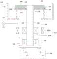
腔室100是真空腔室,适合用于在基板处理期间维持腔室内部空间120中的次大气压(sub-atmospheric pressure)。腔室100包括由盖104覆盖的腔室主体106,所述盖104包围定位于腔室内部空间120的上半部中的处理空间119。腔室100还可包括约束各种腔室部件的一个或多个护罩105,以防止这些部件和离子化的工艺材料之间不必要的反应。腔室主体106和盖104可以金属制成,例如铝。腔室主体106可经由耦合至地线115而接地。The
基板支撑件124布置于腔室内部空间120中,以支撑并且保持诸如半导体晶片的基板S,或例如可电气保持的其他此类基板。基板支撑件124可通常包含静电夹盘150(在下方关于图2-图4将更详细地说明)和用于支撑静电夹盘150的中空支撑轴112。中空支撑轴112提供导管,以将例如工艺气体、流体、冷却剂、功率或诸如此类提供至静电夹盘150。A
在某些实施方式中,中空支撑轴112耦合至诸如致动器或电动机的升降机构(liftmechanism)113,所述升降机构113提供静电夹盘150在上部、处理位置(如图1所示)和下部、传送位置(未示出)之间的竖直移动。波纹管组件110围绕中空支撑轴112布置并且耦合于静电夹盘150和腔室100的底表面126之间,以提供允许静电夹盘150的竖直运动的柔性密封同时防止从腔室100中漏失真空。波纹管组件110还包括与O形环165接触的下部波纹管凸缘164,或与底表面126接触的其他适合的密封元件,以帮助防止腔室真空的漏失。In certain embodiments, the
中空支撑轴112提供导管,所述导管用于将流体源142、气源141、夹持电源140和RF源(例如,RF等离子体电源170和RF偏压电源117)耦合至静电夹盘150。在某些实施方式中,RF等离子体电源170和RF偏压电源117经由相应的RF匹配网络(仅示出RF匹配网络116)耦合至静电夹盘。
基板升降器130可包括安装于连接至轴111的平台108上的升降杆109,轴111耦合至第二升降机构132,用于升起和降低基板升降器130,使得基板“S”可放置于静电夹盘150上或从静电夹盘150移除。静电夹盘150包括通孔(以下将说明)以容纳升降杆109。波纹管组件131耦合于基板升降器130和底表面126之间,以提供在基板升降器130的竖直运动期间维持腔室真空的柔性密封。The
腔室100耦合至真空系统114并且与真空系统114流体连通,真空系统114包括节流阀(未示出)和用于抽空腔室100的真空泵(未示出)。在腔室100内部的压力可通过调整节流阀和/或真空泵而调节。腔室100还耦接至工艺气源118并且与工艺气源118流体连通,工艺气源118可供应一种或多种工艺气体至腔室100,用于处理布置于腔室100中的基板。The
举例而言,在操作中可在腔室内部空间120中产生等离子体102,以实行一种或多种工艺。等离子体102可通过从等离子体功率源(例如,RF等离子体电源170)经由靠近腔室内部空间120或在腔室内部空间120中的一个或多个电极来耦合功率至工艺气体而产生,以点燃(ignite)工艺气体并且产生等离子体102。在某些实施方式中,也可从偏压电源(例如,RF偏压电源117)经由电容耦合的偏压板(以下将说明)提供偏压功率至布置于静电夹盘150中的一个或多个电极(以下将说明),以从等离子体吸引离子朝向基板S。In operation, for example,
举例而言,在腔室100是PVD腔室的某些实施方式中,包含待沉积于基板S上的源材料的靶166可布置于基板上方并且在腔室内部空间120中。靶166可由腔室100的接地的导电部分支撑,例如经由介电绝缘器的铝适配器。在其他实施方式中,腔室100可包括多阴极排列中的多个靶,用于使用相同的腔室沉积不同材料的层。For example, in certain embodiments where
可控制的DC功率源168可耦合至腔室100以施加负电压或偏压至靶166。RF偏压电源117可耦合至基板支撑件124,以引起在基板S上的负DC偏压。此外,在某些实施方式中,负DC自偏压可在处理期间形成于基板S上。在某些实施方式中,RF等离子体电源170也可耦合至腔室100以施加RF功率至靶166,而促进对基板S上沉积速率的径向分布的控制。在操作中,腔室100中产生的等离子体102中的离子与来自靶166的源材料反应。反应造成靶166射出源材料的原子,源材料的原子接着导向基板S,因此沉积材料。A controllable
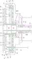
图2根据本公开内容的实施方式,描绘静电夹盘(夹盘200)的横截面图。夹盘200包括盘(disk)202,从盘202底部延伸的轴204,和包围盘202、轴204与夹盘200的其他部件(以下将说明)的壳体206。FIG. 2 depicts a cross-sectional view of an electrostatic chuck (chuck 200 ), according to an embodiment of the disclosure.
盘202以诸如陶瓷材料的介电材料形成,例如氮化铝、氧化铝、氮化硼、掺杂有氧化钛的氧化铝和诸如此类。盘202包括接近盘202的上表面布置的一个或多个夹持电极208。盘202包括用于支撑基板(未示出)的支撑表面和相对的第二表面。一个或多个夹持电极208以适合的导电材料制成,例如钼、钛或诸如此类。一个或多个夹持电极208可以任何将在处理期间充分地将基板固定至盘的上表面的配置而安排。举例而言,一个或多个夹持电极208可经安排以提供单一电极静电夹盘、双极静电夹盘或诸如此类。
如上所述,盘202也可包括一个或多个RF偏压电极210。一个或多个RF偏压电极210电容耦合至RF功率,以从等离子体吸引离子朝向布置于盘202上的基板。功率经由可旋转RF耦合装置300(以下将说明)输送至RF偏压电极210,可旋转RF耦合装置300从外部RF功率源(例如,RF偏压电源117)接收功率。可旋转RF耦合装置300电容耦合至RF偏压电极210,因而移除横跨导体的任何直接的电气耦合。因此,可在盘202旋转的同时输送功率至RF偏压电极210。As mentioned above,
为了促进盘202和当被布置于盘上时基板的加热,夹盘200包括多个灯214。多个灯214可布置于灯笼211中,灯笼211包括灯壳体216,灯壳体216收容多个灯214和布置于多个灯214上方以保护灯不受RF能量的影响的RF护罩212(例如,法拉第笼(Faraday cage))。灯壳体216以能够承受多个灯214的热的材料形成。举例而言,灯壳体216可以陶瓷材料形成。多个灯214包括能够发射足够热以通过辐射加热盘202的任何类型的灯。举例而言,多个灯214可包括卤素灯。To facilitate heating of the
RF护罩212设计为允许由多个灯214产生的热通过RF护罩212到达盘202,举例而言,在某些实施方式中,RF护罩可包括布置于每个灯214上方的开口213。替代地,在某些实施方式中,RF护罩可以是网状物(mesh),网状物允许热通过网孔,同时保护灯214不受RF能量的影响。因此RF护罩212有利地防止或限制RF能量耦合至多个灯214,同时允许来自多个灯214的热能到达盘202。在某些实施方式中,RF护罩212以例如用于在高达约750℃的温度下使用的的钼或例如用于在高达约250℃的温度下使用的抛光铝形成。RF护罩212可由夹(clamp)236保持在位。举例而言,夹236可包括外安装环232和内安装环234,外安装环232和内安装环234可各自栓接(bolted)或用其他方法固定至灯壳体216,同时夹或保持RF护罩212在位。The
夹盘200还可包括靠近于盘202定位的轴承218(举例而言,在盘202的约3英寸内),以提供旋转期间对夹盘200的增强的稳定性(rigidity)。轴承218可包括例如交叉滚子轴承或诸如此类。金属板220布置于灯壳体216的下方,以将热传导离开轴承218,否则可造成轴承膨胀并且最终卡住。金属板220可以任何处理相容的金属或金属合金形成,例如铝。金属板220经依一定尺寸制造,使得间隙布置于金属板220的外边缘和壳体206的内表面之间。在夹盘200操作期间,由多个灯214产生的热加热金属板220,造成金属板220热膨胀,使得金属板220的外直径或边缘接触壳体206的内表面。在接触壳体206的内表面之后,金属板220立即通过传导传送热至壳体206。流体通道(以下将说明)可布置于壳体206中,以流动传热流体(例如,冷却剂)来冷却壳体206。The
夹盘200进一步包括旋转组件(即,磁性驱动组件222)以旋转盘202。磁性驱动组件222包括内磁体222A和外磁体222B。内磁体222A附接或固定至轴204。在某些实施方式中,内磁体222A附接至轴204的下部靠近轴204相对于盘202的一端。外磁体222B布置于壳体206的外侧靠近内磁体222A。外磁体222B可由适合的机构驱动,例如由带驱动或电动机,以驱动内磁体222A、和轴204与盘202。因为内磁体222A布置于壳体206中,所以内磁体222A处于真空压力,因为外磁体222B布置于壳体206外侧,所以外磁体222B处于大气压力。然而,内磁体222A和外磁体222B两者可替代地都布置于壳体206中。因此,磁性驱动组件222使盘202和轴204相对于保持静止的工艺腔室和夹盘200其余的部件(例如,壳体206、灯笼211、金属板220和诸如此类)旋转。或者,磁性驱动组件222可使用其他配置以旋转盘202和轴204。举例而言,在某些实施方式中,内磁体222A和外磁体222B可分别作用为转子及定子,而具有导体缠绕于定子周围以电磁驱动转子。The
夹盘200还包括轴承组件224,轴承组件224位于轴204相对于盘202的一端处。轴承组件224支撑轴204并且促进轴204的旋转。此外,发明人已提供改善的方式,以通过轴承组件224将功率路由至夹持电极208,来促进在旋转夹盘200的同时提供功率至夹持电极208。功率从DC功率源226提取通过壳体206中的连接并且路由至轴承组件224。电流流动通过轴承组件224,并且随后经由布置于轴204内部中的夹持功率线228路由至夹持电极208。为了防止夹持电源(例如,DC功率源226)的任何干扰,轴承组件可耦合至绝缘体230,绝缘体230耦合至壳体206的内部。The
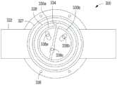
图3A根据本公开内容的某些实施方式,描绘可旋转RF耦合装置300(以下称为“耦合装置300”)的横截面图。图3B描绘耦合装置300的俯视图。耦合装置300包括接地护罩322,接地护罩322内部布置耦合至导电板325的多个RF输入抽头324、耦合至导电板325的导电静置环328、和具有第一半部330a与第二半部330b的导电可旋转对分圆柱330。例如通过从RF输入抽头324路由出腔室并且到RF匹配网络116的一个或多个RF电缆,或一些其他电气耦合至RF匹配网络116的部件,多个RF输入抽头324电气耦合至RF偏压电源117和RF匹配网络116。一个或多个介电绝缘体326、327布置于护罩322与导电板325和静置环328之间以防止发弧(arcing)。3A depicts a cross-sectional view of a rotatable RF coupling device 300 (hereinafter "
可旋转RF耦合装置300可经由RF输入抽头324,从RF偏压电源117或从另一功率源(未示出)接收功率。陶瓷圆柱332布置于可旋转对分圆柱330的下方有利地防止来自RF波的夹持电源的干扰。Rotatable
间隙334形成于静置环328和可旋转对分圆柱330之间。在某些实施方式中,间隙334具有在约0.003英寸至约0.01英寸之间的宽度。在使用期间,RF功率流动通过多个RF输入抽头324、通过导电板325、通过静置环328并且横跨间隙334,以耦合RF能量至可旋转对分圆柱330,可旋转对分圆柱330耦合至含有一个或多个夹持电极208和RF偏压电极210的盘202。发明人已发现横跨间隙334的RF能量的电容耦合有利地允许隔绝的(isolated)并且由接地电位环绕的RF耦合,以防止发弧或放电。发明人还发现电容损失为介于供应至多个RF输入抽头324的RF功率的约10-15%。A
耦合装置300可包括多个电气抽头,以耦合功率至盘202中的夹持电极。举例而言,如图3B中所描绘,三个电气抽头:第一、第二和第三电气抽头338a、338b和338c延伸穿过可旋转对分圆柱330。布置于第一半部330a中的第一电气抽头338a可携带正或负电压,而布置于第二半部330b中的第二电气抽头338b携带与电气抽头338a相反的极性的电压。第三电气抽头338c作用为浮动电位(floating potential)并且未耦合至电源。对分圆柱330耦合至夹持电源,以供应电气抽头用于夹持电极308的DC功率。护罩322可包括多个通孔336,固定元件(螺钉、螺栓等等)可延伸穿过通孔336以将可旋转RF耦合装置300耦合至轴承218。
图3C描绘包括可旋转RF耦合装置300的夹盘200的横截面图。多个灯214从布置于介电板302(例如陶瓷板)中的多个导体304接收功率。导体304可从DC功率源226接收功率。在某些实施方式中,介电层306可布置于介电板302顶上,以保护导体304并且防止导体304和夹盘200的任何其他导电元件之间的非故意的接触。提供在介电层306中的开口以促进将导体304耦合至相应的灯214。可旋转RF耦合装置300延伸穿过灯壳体216和金属板220,并且于可旋转RF耦合装置300的第一端处耦合至盘202,来以与灯壳体216隔开的关系支撑盘202。在某些实施方式中,多个灯可划分成多个区,例如图4中所图示的内灯阵列和可独立控制的外灯阵列。FIG. 3C depicts a cross-sectional view of
如以上所解释,当启动多个灯214时,立即产生热并且加热盘202。因为热朝所有方向发射而不仅朝向盘202,所以金属板220布置于灯壳体216下方以吸收热。在吸收工艺期间,金属板220膨胀并且开始延伸至介于金属板220的外边缘和壳体206之间的间隙316中。在接触壳体206之后,金属板220立即传送热至壳体206。为了保持壳体206冷却,多个流体通道可形成于壳体206中。任何适合的冷却剂(例如,水、丙二醇或诸如此类)可流动通过流体通道以冷却壳体206。As explained above, when the plurality of
在某些实施方式中,夹盘200可包括扭力弹簧340以确保耦合装置300与夹盘200的其余部分适当地对准。为了促进基板在盘202上的放置和移除,夹盘200还可包括升降杆组件,升降杆组件包括多个升降杆314以升起和降低基板离开盘202或到盘202上。在某些实施方式中,多个升降杆314中的至少一个可包括高温计,以测量盘202的温度。盘202相对于升降杆314布置的区域可经处理以具有非常高的发射率(emissivity),来促进通过高温计监测盘202的温度。In some embodiments, the
图4根据本公开内容的某些实施方式,描绘灯笼的俯视图。如以上所解释,灯笼的RF护罩(图2所示的RF护罩212)允许由多个灯214产生的热加热盘202。由于RF护罩的特性,并且特别是RF护罩是网状物的实施方式,为了不遮蔽余下的细节,在图4的俯视图中未示出RF护罩。在某些实施方式中,RF护罩或网状物可由内安装环404和外安装环407保持在位。RF护罩212和灯壳体216还包括中心孔402和多个孔406,中心孔402允许轴204穿过中心孔402,多个孔406允许多个升降杆314穿过多个孔406。尽管显示为以特定配置安排的狭缝,可改变开口的形状和数量以及灯的形状和数量,以在盘202上提供期望的热分布。Figure 4 depicts a top view of a lantern, according to certain embodiments of the present disclosure. As explained above, the lantern's RF shield (
尽管以上针对本公开内容的实施方式,可设计本公开内容的其他和进一步的实施方式而不悖离本公开内容的基本范围。While the above is directed to embodiments of the present disclosure, other and further embodiments of the present disclosure can be devised without departing from the basic scope of the present disclosure.
Claims (15)
Translated fromChineseApplications Claiming Priority (3)
| Application Number | Priority Date | Filing Date | Title |
|---|---|---|---|
| US201562247745P | 2015-10-28 | 2015-10-28 | |
| US62/247,745 | 2015-10-28 | ||
| PCT/US2016/059500WO2017075474A1 (en) | 2015-10-28 | 2016-10-28 | Biasable rotatable electrostatic chuck |
Publications (2)
| Publication Number | Publication Date |
|---|---|
| CN108352352A CN108352352A (en) | 2018-07-31 |
| CN108352352Btrue CN108352352B (en) | 2023-05-09 |
Family
ID=58631219
Family Applications (1)
| Application Number | Title | Priority Date | Filing Date |
|---|---|---|---|
| CN201680062275.5AActiveCN108352352B (en) | 2015-10-28 | 2016-10-28 | Biasable rotatable electrostatic chuck |
Country Status (7)
| Country | Link |
|---|---|
| US (1) | US10490434B2 (en) |
| EP (1) | EP3369109B1 (en) |
| JP (1) | JP6869978B2 (en) |
| KR (1) | KR102657486B1 (en) |
| CN (1) | CN108352352B (en) |
| TW (1) | TWI725067B (en) |
| WO (1) | WO2017075474A1 (en) |
Families Citing this family (12)
| Publication number | Priority date | Publication date | Assignee | Title |
|---|---|---|---|---|
| US9887120B2 (en)* | 2015-11-03 | 2018-02-06 | Lam Research Ag | Apparatus for treating surfaces of wafer-shaped articles |
| US10784139B2 (en) | 2016-12-16 | 2020-09-22 | Applied Materials, Inc. | Rotatable electrostatic chuck having backside gas supply |
| US10573498B2 (en) | 2017-01-09 | 2020-02-25 | Applied Materials, Inc. | Substrate processing apparatus including annular lamp assembly |
| WO2018230883A1 (en)* | 2017-06-16 | 2018-12-20 | 주성엔지니어링(주) | Substrate processing apparatus and rotary electric connector for vacuum |
| CN118380371A (en)* | 2017-11-21 | 2024-07-23 | 朗姆研究公司 | Bottom edge ring and middle edge ring |
| US11149345B2 (en) | 2017-12-11 | 2021-10-19 | Applied Materials, Inc. | Cryogenically cooled rotatable electrostatic chuck |
| US11562890B2 (en) | 2018-12-06 | 2023-01-24 | Applied Materials, Inc. | Corrosion resistant ground shield of processing chamber |
| CN110265323B (en)* | 2019-05-31 | 2021-09-03 | 拓荆科技股份有限公司 | Wafer heating seat with contact array |
| US12112972B2 (en) | 2021-04-02 | 2024-10-08 | Applied Materials, Inc. | Rotating biasable pedestal and electrostatic chuck in semiconductor process chamber |
| KR102589182B1 (en)* | 2021-08-31 | 2023-10-16 | 피에스케이 주식회사 | Apparatus for treating substrate and method for aligning dielectric plate using the same |
| CN115632029B (en)* | 2022-12-22 | 2023-03-17 | 河北博特半导体设备科技有限公司 | Ceramic rotating platform structure of high-precision wafer bearing platform |
| GB202319929D0 (en)* | 2023-12-22 | 2024-02-07 | Spts Technologies Ltd | Pvd apparatus and method |
Citations (1)
| Publication number | Priority date | Publication date | Assignee | Title |
|---|---|---|---|---|
| US5708250A (en)* | 1996-03-29 | 1998-01-13 | Lam Resarch Corporation | Voltage controller for electrostatic chuck of vacuum plasma processors |
Family Cites Families (12)
| Publication number | Priority date | Publication date | Assignee | Title |
|---|---|---|---|---|
| US4170541A (en)* | 1978-08-14 | 1979-10-09 | Varian Associates, Inc. | Rotating resonator for large substrate tables in sputtering systems |
| US6132517A (en)* | 1997-02-21 | 2000-10-17 | Applied Materials, Inc. | Multiple substrate processing apparatus for enhanced throughput |
| JP2003133233A (en) | 2001-10-23 | 2003-05-09 | Hitachi Kokusai Electric Inc | Substrate processing equipment |
| US6875927B2 (en)* | 2002-03-08 | 2005-04-05 | Applied Materials, Inc. | High temperature DC chucking and RF biasing cable with high voltage isolation for biasable electrostatic chuck applications |
| JP4768699B2 (en)* | 2006-11-30 | 2011-09-07 | キヤノンアネルバ株式会社 | Power introduction apparatus and film forming method |
| WO2012011149A1 (en) | 2010-07-21 | 2012-01-26 | キヤノンアネルバ株式会社 | Power input device and vacuum processing apparatus using power input device |
| US20120222618A1 (en)* | 2011-03-01 | 2012-09-06 | Applied Materials, Inc. | Dual plasma source, lamp heated plasma chamber |
| KR101625318B1 (en)* | 2011-12-13 | 2016-05-27 | 캐논 아네르바 가부시키가이샤 | Power introduction device and vacuum processing device |
| US20150004798A1 (en)* | 2013-06-28 | 2015-01-01 | Lam Research Corporation | Chemical deposition chamber having gas seal |
| US9490149B2 (en)* | 2013-07-03 | 2016-11-08 | Lam Research Corporation | Chemical deposition apparatus having conductance control |
| US20150083042A1 (en)* | 2013-09-26 | 2015-03-26 | Applied Materials, Inc. | Rotatable substrate support having radio frequency applicator |
| US9853579B2 (en)* | 2013-12-18 | 2017-12-26 | Applied Materials, Inc. | Rotatable heated electrostatic chuck |
- 2016
- 2016-10-26TWTW105134497Apatent/TWI725067B/enactive
- 2016-10-28CNCN201680062275.5Apatent/CN108352352B/enactiveActive
- 2016-10-28USUS15/337,942patent/US10490434B2/enactiveActive
- 2016-10-28JPJP2018521344Apatent/JP6869978B2/enactiveActive
- 2016-10-28WOPCT/US2016/059500patent/WO2017075474A1/ennot_activeCeased
- 2016-10-28EPEP16860958.4Apatent/EP3369109B1/enactiveActive
- 2016-10-28KRKR1020187015080Apatent/KR102657486B1/enactiveActive
Patent Citations (1)
| Publication number | Priority date | Publication date | Assignee | Title |
|---|---|---|---|---|
| US5708250A (en)* | 1996-03-29 | 1998-01-13 | Lam Resarch Corporation | Voltage controller for electrostatic chuck of vacuum plasma processors |
Also Published As
| Publication number | Publication date |
|---|---|
| KR20180061421A (en) | 2018-06-07 |
| US10490434B2 (en) | 2019-11-26 |
| US20170125274A1 (en) | 2017-05-04 |
| EP3369109A1 (en) | 2018-09-05 |
| KR102657486B1 (en) | 2024-04-12 |
| JP2019503066A (en) | 2019-01-31 |
| TW201721799A (en) | 2017-06-16 |
| JP6869978B2 (en) | 2021-05-12 |
| EP3369109A4 (en) | 2019-03-13 |
| CN108352352A (en) | 2018-07-31 |
| TWI725067B (en) | 2021-04-21 |
| EP3369109B1 (en) | 2021-01-06 |
| WO2017075474A1 (en) | 2017-05-04 |
Similar Documents
| Publication | Publication Date | Title |
|---|---|---|
| CN108352352B (en) | Biasable rotatable electrostatic chuck | |
| US9853579B2 (en) | Rotatable heated electrostatic chuck | |
| CN110050334B (en) | Rotatable electrostatic chuck with backside gas source | |
| US10978276B2 (en) | Substrate processing apparatus including top reflector above annular lamp assembly | |
| JP2023517716A (en) | Sheath and temperature control for process kits in substrate processing chambers | |
| CN105027274A (en) | Substrate Support Chuck Cooling for Deposition Chambers | |
| CN107004628A (en) | The electrostatic chuck applied for high temperature RF |
Legal Events
| Date | Code | Title | Description |
|---|---|---|---|
| PB01 | Publication | ||
| PB01 | Publication | ||
| SE01 | Entry into force of request for substantive examination | ||
| SE01 | Entry into force of request for substantive examination | ||
| GR01 | Patent grant | ||
| GR01 | Patent grant | ||
| TG01 | Patent term adjustment | ||
| TG01 | Patent term adjustment |