CN108304086B - Touch control display device - Google Patents
Touch control display deviceDownload PDFInfo
- Publication number
- CN108304086B CN108304086BCN201710019694.7ACN201710019694ACN108304086BCN 108304086 BCN108304086 BCN 108304086BCN 201710019694 ACN201710019694 ACN 201710019694ACN 108304086 BCN108304086 BCN 108304086B
- Authority
- CN
- China
- Prior art keywords
- touch
- display device
- layer
- touch display
- insulating layer
- Prior art date
- Legal status (The legal status is an assumption and is not a legal conclusion. Google has not performed a legal analysis and makes no representation as to the accuracy of the status listed.)
- Active
Links
Images


Classifications
- G—PHYSICS
- G06—COMPUTING OR CALCULATING; COUNTING
- G06F—ELECTRIC DIGITAL DATA PROCESSING
- G06F3/00—Input arrangements for transferring data to be processed into a form capable of being handled by the computer; Output arrangements for transferring data from processing unit to output unit, e.g. interface arrangements
- G06F3/01—Input arrangements or combined input and output arrangements for interaction between user and computer
- G06F3/03—Arrangements for converting the position or the displacement of a member into a coded form
- G06F3/041—Digitisers, e.g. for touch screens or touch pads, characterised by the transducing means
- G06F3/0412—Digitisers structurally integrated in a display
- G—PHYSICS
- G06—COMPUTING OR CALCULATING; COUNTING
- G06F—ELECTRIC DIGITAL DATA PROCESSING
- G06F3/00—Input arrangements for transferring data to be processed into a form capable of being handled by the computer; Output arrangements for transferring data from processing unit to output unit, e.g. interface arrangements
- G06F3/01—Input arrangements or combined input and output arrangements for interaction between user and computer
- G06F3/03—Arrangements for converting the position or the displacement of a member into a coded form
- G06F3/041—Digitisers, e.g. for touch screens or touch pads, characterised by the transducing means
- G06F3/0416—Control or interface arrangements specially adapted for digitisers
- G06F3/04164—Connections between sensors and controllers, e.g. routing lines between electrodes and connection pads
- G—PHYSICS
- G06—COMPUTING OR CALCULATING; COUNTING
- G06F—ELECTRIC DIGITAL DATA PROCESSING
- G06F3/00—Input arrangements for transferring data to be processed into a form capable of being handled by the computer; Output arrangements for transferring data from processing unit to output unit, e.g. interface arrangements
- G06F3/01—Input arrangements or combined input and output arrangements for interaction between user and computer
- G06F3/03—Arrangements for converting the position or the displacement of a member into a coded form
- G06F3/041—Digitisers, e.g. for touch screens or touch pads, characterised by the transducing means
- G06F3/044—Digitisers, e.g. for touch screens or touch pads, characterised by the transducing means by capacitive means
- G06F3/0443—Digitisers, e.g. for touch screens or touch pads, characterised by the transducing means by capacitive means using a single layer of sensing electrodes
- G—PHYSICS
- G06—COMPUTING OR CALCULATING; COUNTING
- G06F—ELECTRIC DIGITAL DATA PROCESSING
- G06F3/00—Input arrangements for transferring data to be processed into a form capable of being handled by the computer; Output arrangements for transferring data from processing unit to output unit, e.g. interface arrangements
- G06F3/01—Input arrangements or combined input and output arrangements for interaction between user and computer
- G06F3/03—Arrangements for converting the position or the displacement of a member into a coded form
- G06F3/041—Digitisers, e.g. for touch screens or touch pads, characterised by the transducing means
- G06F3/044—Digitisers, e.g. for touch screens or touch pads, characterised by the transducing means by capacitive means
- G06F3/0446—Digitisers, e.g. for touch screens or touch pads, characterised by the transducing means by capacitive means using a grid-like structure of electrodes in at least two directions, e.g. using row and column electrodes
- H—ELECTRICITY
- H01—ELECTRIC ELEMENTS
- H01L—SEMICONDUCTOR DEVICES NOT COVERED BY CLASS H10
- H01L25/00—Assemblies consisting of a plurality of semiconductor or other solid state devices
- H01L25/16—Assemblies consisting of a plurality of semiconductor or other solid state devices the devices being of types provided for in two or more different subclasses of H10B, H10D, H10F, H10H, H10K or H10N, e.g. forming hybrid circuits
- H01L25/167—Assemblies consisting of a plurality of semiconductor or other solid state devices the devices being of types provided for in two or more different subclasses of H10B, H10D, H10F, H10H, H10K or H10N, e.g. forming hybrid circuits comprising optoelectronic devices, e.g. LED, photodiodes
- H—ELECTRICITY
- H10—SEMICONDUCTOR DEVICES; ELECTRIC SOLID-STATE DEVICES NOT OTHERWISE PROVIDED FOR
- H10K—ORGANIC ELECTRIC SOLID-STATE DEVICES
- H10K59/00—Integrated devices, or assemblies of multiple devices, comprising at least one organic light-emitting element covered by group H10K50/00
- H10K59/10—OLED displays
- H10K59/12—Active-matrix OLED [AMOLED] displays
- H10K59/131—Interconnections, e.g. wiring lines or terminals
- H—ELECTRICITY
- H10—SEMICONDUCTOR DEVICES; ELECTRIC SOLID-STATE DEVICES NOT OTHERWISE PROVIDED FOR
- H10K—ORGANIC ELECTRIC SOLID-STATE DEVICES
- H10K59/00—Integrated devices, or assemblies of multiple devices, comprising at least one organic light-emitting element covered by group H10K50/00
- H10K59/40—OLEDs integrated with touch screens
- G—PHYSICS
- G06—COMPUTING OR CALCULATING; COUNTING
- G06F—ELECTRIC DIGITAL DATA PROCESSING
- G06F2203/00—Indexing scheme relating to G06F3/00 - G06F3/048
- G06F2203/041—Indexing scheme relating to G06F3/041 - G06F3/045
- G06F2203/04103—Manufacturing, i.e. details related to manufacturing processes specially suited for touch sensitive devices
- H—ELECTRICITY
- H10—SEMICONDUCTOR DEVICES; ELECTRIC SOLID-STATE DEVICES NOT OTHERWISE PROVIDED FOR
- H10H—INORGANIC LIGHT-EMITTING SEMICONDUCTOR DEVICES HAVING POTENTIAL BARRIERS
- H10H20/00—Individual inorganic light-emitting semiconductor devices having potential barriers, e.g. light-emitting diodes [LED]
- H10H20/80—Constructional details
- H10H20/85—Packages
- H10H20/852—Encapsulations
- H—ELECTRICITY
- H10—SEMICONDUCTOR DEVICES; ELECTRIC SOLID-STATE DEVICES NOT OTHERWISE PROVIDED FOR
- H10K—ORGANIC ELECTRIC SOLID-STATE DEVICES
- H10K59/00—Integrated devices, or assemblies of multiple devices, comprising at least one organic light-emitting element covered by group H10K50/00
- H10K59/80—Constructional details
- H10K59/87—Passivation; Containers; Encapsulations
- H10K59/873—Encapsulations
Landscapes
- Engineering & Computer Science (AREA)
- General Engineering & Computer Science (AREA)
- Theoretical Computer Science (AREA)
- Physics & Mathematics (AREA)
- General Physics & Mathematics (AREA)
- Human Computer Interaction (AREA)
- Microelectronics & Electronic Packaging (AREA)
- Computer Networks & Wireless Communication (AREA)
- Power Engineering (AREA)
- Computer Hardware Design (AREA)
- Condensed Matter Physics & Semiconductors (AREA)
- Devices For Indicating Variable Information By Combining Individual Elements (AREA)
- Position Input By Displaying (AREA)
- Electroluminescent Light Sources (AREA)
- Electromagnetism (AREA)
- Electrophonic Musical Instruments (AREA)
- Fittings On The Vehicle Exterior For Carrying Loads, And Devices For Holding Or Mounting Articles (AREA)
- Push-Button Switches (AREA)
- Illuminated Signs And Luminous Advertising (AREA)
- Switches That Are Operated By Magnetic Or Electric Fields (AREA)
Abstract
Translated fromChinese
Description
Translated fromChinese技术领域technical field
本实施例涉及一种触控显示装置,尤其涉及一种包括发光组件的的触控显示装置。This embodiment relates to a touch display device, and more particularly, to a touch display device including a light-emitting component.
背景技术Background technique
近年来,随着信息技术、无线移动通信和信息家电等各项应用的快速发展,为了达到更便利、体积更轻巧化以及更人性化的目的,许多信息产品的输入装置已由传统的键盘或鼠标等转变为触控显示装置。常见的触控显示装置可以是在显示面板与触控面板分别制造完成后,再将两者贴合在一起或是组装在一起而实现触控功能与显示功能的整合。然而,以这种方式制造的触控显示装置,其体积无法精简,而不符合市场对电子产品的需求。因此,已有将触控组件整合于显示面板的技术被提出。In recent years, with the rapid development of various applications such as information technology, wireless mobile communication and information appliances, in order to achieve the purpose of being more convenient, lighter in size and more user-friendly, the input devices of many information products have been replaced by traditional keyboards or A mouse or the like is transformed into a touch display device. In a common touch display device, after the display panel and the touch panel are manufactured separately, the two are bonded together or assembled together to realize the integration of the touch function and the display function. However, the volume of the touch display device manufactured in this way cannot be reduced, which does not meet the market demand for electronic products. Therefore, technologies for integrating touch components into display panels have been proposed.
发明内容SUMMARY OF THE INVENTION
依据一些实施例,触控显示装置包括基板、发光组件、第一绝缘层、第一触控部以及第一传输部。基板具有显示区和周边区。发光组件设置于所述显示区上。第一绝缘层设置于所述显示区和所述周边区上,且覆盖所述发光组件。第一触控部设置于所述第一绝缘层上,所述第一触控部的至少一部分位于所述显示区上。第一传输部设置于所述第一绝缘层上且设置于所述周边区上,与所述第一触控部电性连接。所述第一传输部与一处理单元电性连接以进行信号传输。According to some embodiments, a touch display device includes a substrate, a light emitting component, a first insulating layer, a first touch portion, and a first transmission portion. The substrate has a display area and a peripheral area. The light-emitting component is arranged on the display area. The first insulating layer is disposed on the display area and the peripheral area, and covers the light emitting element. The first touch part is disposed on the first insulating layer, and at least a part of the first touch part is located on the display area. The first transmission part is disposed on the first insulating layer and the peripheral region, and is electrically connected with the first touch part. The first transmission part is electrically connected with a processing unit for signal transmission.
基于上述,本发明实施例的触控显示装置中,触控部和发光组件设置在相同基板上,达到触控和显示的整合。第一绝缘层设置在发光组件上,且第一传输部设置在第一绝缘层上,达到传递触控信号的目的。Based on the above, in the touch display device according to the embodiment of the present invention, the touch part and the light-emitting component are disposed on the same substrate, so as to achieve the integration of touch and display. The first insulating layer is arranged on the light-emitting component, and the first transmission part is arranged on the first insulating layer, so as to achieve the purpose of transmitting touch signals.
附图说明Description of drawings
包含附图以便进一步理解本发明,且附图并入本说明书中并构成本说明书的一部分。附图说明本发明的实施例,并与描述一起用于解释本发明的原理。The accompanying drawings are included to provide a further understanding of the present invention, and are incorporated in and constitute a part of this specification. The drawings illustrate embodiments of the invention and together with the description serve to explain the principles of the invention.
图1A为本发明第一实施例的触控显示装置的局部上视示意图;FIG. 1A is a schematic partial top view of a touch display device according to a first embodiment of the present invention;
图1B为图1A的触控显示装置沿线I-I的剖面示意图;FIG. 1B is a schematic cross-sectional view of the touch display device of FIG. 1A along line I-I;
图1C为图1B的触控显示装置在虚线框C中以微发光二极管作为发光组件的变化例的示意图;FIG. 1C is a schematic diagram of a variation of the touch display device in FIG. 1B in which micro-LEDs are used as light-emitting components in the dotted frame C;
图2为本发明第一实施例的触控显示装置的变化例的剖面示意图;2 is a schematic cross-sectional view of a modification of the touch display device according to the first embodiment of the present invention;
图3A、图3B、图3C为本发明第二实施例的触控显示装置的剖面示意图;3A, 3B, and 3C are schematic cross-sectional views of a touch display device according to a second embodiment of the present invention;
图4为本发明第二实施例的触控显示装置的变化例的剖面示意图;4 is a schematic cross-sectional view of a modification of the touch display device according to the second embodiment of the present invention;
图5为本发明第三实施例的触控显示装置的剖面示意图;5 is a schematic cross-sectional view of a touch display device according to a third embodiment of the present invention;
图6为本发明第三实施例的触控显示装置的变化例的剖面示意图;6 is a schematic cross-sectional view of a modification of the touch display device according to the third embodiment of the present invention;
图7为本发明第四实施例的触控显示装置的剖面示意图;7 is a schematic cross-sectional view of a touch display device according to a fourth embodiment of the present invention;
图8为本发明第四实施例的触控显示装置的变化例的剖面示意图;8 is a schematic cross-sectional view of a modification of the touch display device according to the fourth embodiment of the present invention;
图9为本发明第五实施例的触控显示装置的剖面示意图;9 is a schematic cross-sectional view of a touch display device according to a fifth embodiment of the present invention;
图10为本发明第五实施例的触控显示装置的变化例的剖面示意图;10 is a schematic cross-sectional view of a modification of the touch display device according to the fifth embodiment of the present invention;
图11A为本发明第六实施例的触控显示装置的局部上视示意图;11A is a schematic partial top view of a touch display device according to a sixth embodiment of the present invention;
图11B为图11A的触控显示装置沿线II-II的剖面示意图;11B is a schematic cross-sectional view of the touch display device of FIG. 11A along line II-II;
图11C为本发明第六实施例的触控显示装置的变化例的剖面示意图;11C is a schematic cross-sectional view of a modification of the touch display device according to the sixth embodiment of the present invention;
图12A为图11B的触控显示装置的变化例的剖面示意图;12A is a schematic cross-sectional view of a modification of the touch display device of FIG. 11B ;
图12B为图11C的触控显示装置的变化例的剖面示意图;12B is a schematic cross-sectional view of a modification of the touch display device of FIG. 11C ;
图13A为本发明第七实施例的触控显示装置的局部上视示意图;13A is a schematic partial top view of a touch display device according to a seventh embodiment of the present invention;
图13B为图13A的触控显示装置沿线III-III的剖面示意图;13B is a schematic cross-sectional view of the touch display device of FIG. 13A along line III-III;
图14为本发明第七实施例的触控显示装置的变化例的剖面示意图;14 is a schematic cross-sectional view of a modification of the touch display device according to the seventh embodiment of the present invention;
图15为本发明第七实施例的触控显示装置的另一变化例的剖面示意图;15 is a schematic cross-sectional view of another variation of the touch display device according to the seventh embodiment of the present invention;
图16A为本发明第八实施例的触控显示装置的局部上视示意图;16A is a schematic partial top view of a touch display device according to an eighth embodiment of the present invention;
图16B为图16A的触控显示装置沿线IV-IV的剖面示意图;16B is a schematic cross-sectional view of the touch display device of FIG. 16A along the line IV-IV;
图17为本发明第八实施例的触控显示装置的变化例的剖面示意图。17 is a schematic cross-sectional view of a modification of the touch display device according to the eighth embodiment of the present invention.
附图标号说明:Description of reference numbers:
100、200、300、300'、300”、400、500、600、700、800、900、1000、1100、1100’、1200、1200’、1300、1400、1500、1600、1700:触控显示装置;100, 200, 300, 300', 300", 400, 500, 600, 700, 800, 900, 1000, 1100, 1100', 1200, 1200', 1300, 1400, 1500, 1600, 1700: touch display device ;
102:基板;102: substrate;
104:显示区;104: display area;
106:周边区;106: surrounding area;
108:发光组件;108: light-emitting components;
109:第一电极;109: the first electrode;
110:第一绝缘层;110: the first insulating layer;
111:发光层;111: light-emitting layer;
112:第一无机层;112: the first inorganic layer;
114:有机层;114: organic layer;
116:第二无机层;116: the second inorganic layer;
118、120:边缘部;118, 120: edge part;
122:触控组件;122: touch component;
124:触控信号传输线;124: touch signal transmission line;
126:第一传输部;126: the first transmission part;
128:第二传输部;128: the second transmission part;
130:第一导接结构;130: the first conducting structure;
132:薄膜晶体管;132: thin film transistor;
134:第一导电层;134: the first conductive layer;
136:第二导电层;136: the second conductive layer;
138:半导体层;138: semiconductor layer;
140:第一介电层;140: a first dielectric layer;
142:第二介电层;142: a second dielectric layer;
144:第三传输部;144: the third transmission part;
145:第四传输部;145: the fourth transmission part;
146:第二导接结构;146: the second conducting structure;
147:第一触控电极;147: a first touch electrode;
148:第一触控部;148: the first touch part;
149:第一连接部;149: the first connecting part;
150:第二触控部;150: the second touch part;
151:第二触控电极;151: a second touch electrode;
152:第三绝缘层;152: the third insulating layer;
153:第二连接部;153: the second connecting part;
154:辅助传输线部;154: auxiliary transmission line part;
155:第三导接结构;155: the third guide structure;
156:对向电极;156: opposite electrode;
158:接合部;158: joint;
160:覆盖层;160: overlay;
162:盖板;162: cover plate;
163:第二绝缘层;163: the second insulating layer;
164:像素定义层;164: pixel definition layer;
166:缓冲层;166: buffer layer;
168:电极;168: electrode;
170:对向电极走线;170: opposite electrode wiring;
172、176、263、272:导接结构;172, 176, 263, 272: guide structure;
174:第三金属层;174: the third metal layer;
178:微发光二极管;178: Micro LED;
180:绝缘材料;180: insulating material;
192:对向导电层;192: opposite conductive layer;
254:第四绝缘层;254: the fourth insulating layer;
264:介电层;264: dielectric layer;
3000:薄膜晶体管层;3000: thin film transistor layer;
A1、A2:区域;A1, A2: area;
BR:架桥;BR: bridge;
C:虚线框;C: dotted frame;
D:漏极;D: drain;
G:栅极;G: grid;
I-I、II-II、III-III、IV-IV:线I-I, II-II, III-III, IV-IV: Lines
10:处理单元;10: processing unit;
S:源极;S: source;
x:第一方向;x: the first direction;
y:第二方向。y: the second direction.
具体实施方式Detailed ways
现将详细地描述本发明的示范性实施例,示范性实施例的实例说明于附图中。只要有可能,相同组件符号在附图和描述中用来表示相同或相似部分。并且,实施例之间可以相互结合,对于相同或相似的概念或过程在某些实施例不再赘述。Reference will now be made in detail to the exemplary embodiments of the present invention, examples of which are illustrated in the accompanying drawings. Wherever possible, the same reference numerals are used in the drawings and description to refer to the same or like parts. In addition, the embodiments may be combined with each other, and the same or similar concepts or processes will not be repeated in some embodiments.
在本发明揭示内容中,在使用“元件A在元件B上”来描述位置关系时,表示可在元件A和元件B之间设置一个或多个的其他元件。或者,也可表示在元件A和元件B之间没有其他元件。In the present disclosure, when "element A is on element B" is used to describe the positional relationship, it means that one or more other elements may be disposed between element A and element B. Alternatively, it may also mean that there are no other elements between element A and element B.
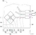
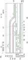
图1A为本发明第一实施例的触控显示装置的局部上视示意图。图1B为图1A的触控显示装置沿线I-I的剖面示意图。FIG. 1A is a schematic partial top view of the touch display device according to the first embodiment of the present invention. FIG. 1B is a schematic cross-sectional view of the touch display device of FIG. 1A along the line I-I.
请同时参看图1A和图1B。触控显示装置100包括基板102、发光组件108、第一绝缘层110、包括第一触控部148的触控组件122以及包括第一传输部126的触控信号传输线124。在本实施例中,可依据最边缘的发光组件108的发光区域的边界作为基板102的显示区104和周边区106的交界。基板102可为软性基板或刚性基板。软性基板的材料包括但不限于塑胶或玻璃。刚性基板的材料包括但不限于玻璃或硅晶圆。发光组件108设置于显示区104上。第一绝缘层110设置于显示区104和周边区106上,且覆盖发光组件108。第一触控部148设置于第一绝缘层110上,第一触控部148的至少一部分位于显示区104上。第一传输部126设置于第一绝缘层110上且设置于周边区106上。第一传输部126与第一触控部148电性连接,以将第一触控部148的信号传递至外部,例如传递至外部的一处理单元10。如图1A所示,第一传输部126可经由一接合部158而与一处理单元10电性连接以进行信号传输。例如,处理单元10可为集成电路。依据一些实施例,第一传输部126可和第一触控部148具有相同材料。例如,第一传输部126和第一触控部148可在相同过程中形成,也即,使用一相同原料层进行图案化而形成。例如,第一传输部126和第一触控部148可为相同层。Please refer to FIG. 1A and FIG. 1B simultaneously. The
触控显示装置100还可包括有源组件阵列(主动组件阵列),其配置于基板102的显示区104中。触控显示装置100可还包括第二绝缘层163,设置于有源组件阵列与发光组件108之间以分隔有源组件阵列与发光组件108。有源组件阵列包括至少一薄膜晶体管132,但不以此为限,有源组件阵列在一实施例中可以包括薄膜晶体管132以外的其他组件,例如电容、传输线等。在本实施例中,薄膜晶体管132是由半导体层138、栅极G、源极S和漏极D构成的组件。栅极G与半导体层138的通道区(未示出)重叠,源极S和漏极D接触半导体层138的通道区的两侧。栅极G由第一导电层134所构成,源极S和漏极D由第二导电层136所构成,其中第一导电层134位于第二导电层136与基板102之间。第二绝缘层163设置于薄膜晶体管132和发光组件108之间。具体而言,第二绝缘层163设置于薄膜晶体管132的第一导电层134和发光组件108之间,且设置于薄膜晶体管132的第二导电层136和发光组件108之间。The
图1B示例性地表示薄膜晶体管132为底栅极的薄膜晶体管(即:栅极G位于半导体层138与基板102之间)。不过,半导体层138也可位于栅极G与基板102之间,而构成顶栅极(topgate)薄膜晶体管。第一导电层134或第二导电层136的材料可为任何已知适用于制作有源组件阵列的金属材料或合适的导电材料,在此不再赘述。可理解有源组件阵列包括所述栅极或所述源极和漏极的至少一金属组件。此外,所述薄膜晶体管132还可以通过多层介电层来分隔不同的金属组件,例如图1B所示的第一介电层140与第二介电层142。第一介电层140位于第一导电层134与半导体层138之间,且第二介电层142位于第二导电层136与半导体层138之间。1B exemplarily shows that the
发光组件108设置于覆盖有源组件阵列的第二绝缘层163上。本实施例可通过像素定义层164来定义出发光组件108的区域范围。发光组件108包括第一电极109、对向电极156和发光层111。发光层111配置于对向电极156与第一电极109之间。发光组件108可由有源组件阵列驱动。以图1B为例,有源组件阵列中的第二导电层136还可包括用于连接至第一电极109的电极168,因此第一电极109可以是通过贯穿第二绝缘层163的导接结构263而电性连接电极168。第一电极109例如可为阳极,而对向电极156例如可为阴极。或者,第一电极109可为阴极,对向电极156可为阳极。发光组件108例如为有机发光二极管(OLED)或微发光二极管(micro-LED)等发光组件,但不限于此。The
在本实施例中,触控显示装置100还可以包括对向电极走线170,其例如是由第二导电层136形成的,但不限于此。以图1B为例,对向电极156例如可通过导接结构272和导接结构172以使对向电极156连接至由第二导电层136形成的对向电极走线170。导接结构272位于像素定义层164内,导接结构172位于第二绝缘层163内。In this embodiment, the
第一绝缘层110覆盖发光组件108与有源组件阵列,可用来阻隔水氧,以保护发光组件。第一绝缘层110可由无机材料和/或有机材料交错堆叠为多层结构所形成。无机材料包括但不限于Al2O3、SiNx或SiOx。有机材料包括但不限于丙烯酸系(acrylic base)材料或聚对二甲苯系(parylene base)材料。只要能够维持第一绝缘层110的阻水氧效果,无机材料和有机材料的堆叠顺序与数量没有特别限制。在本实施例中,第一绝缘层110可包括一第一无机层112以及设置于第一无机层112上的一第二无机层116,但不限于此。触控显示装置100的显示区104上还包括一有机层114,位于第一无机层112与第二无机层116之间。也就是说,第一无机层112和第二无机层116在周边区106直接接触,而在显示区104则位于有机层114的上下两侧。一般来说,有机层114的厚度相对较厚,通过将有机层114的边缘设置成缓坡结构,能够有效减少后续层别于有机层114的边缘处的断线现象。The first insulating
触控显示装置100还可包括第二触控部150以及第三绝缘层152。详细而言,如图1A所示,第一触控部148、第二触控部150以及第三绝缘层152可构成触控组件122。和前述第一触控部148类似地,第二触控部150也可与处理单元10电性连接进行信号传输。第二触控部150可经由和上述第一触控部148类似的方式,经由包括传输部的触控信号传输线,而与处理单元10电性连接,在此不再赘述。The
在本实施例中,触控显示装置的触控型式为互容式,第一触控部148可为驱动电极,用以接收驱动信号,第二触控部150可为感测电极,用以将感测信号回传到处理单元。或者,第一触控部148可为感测电极,第二触控部150可为驱动电极。在其他实施例中,触控显示装置的触控型式也可为自容式。In this embodiment, the touch type of the touch display device is a mutual capacitance type, the
第一触控部148包括多数个第一触控电极147以及多数个第一连接部149。多数个第一触控电极147沿着第一方向x排列,且通过多数个第一连接部149彼此电性连接。第二触控部150包括多数个第二触控电极151以及多数个第二连接部153。多数个第二触控电极151沿着第二方向y排列,第一方向x和第二方向y不同(第一方向x和第二方向y例如为彼此正交,但也可以采用非正交方式相交)。其中,多数个第二触控电极151通过多数个第二连接部153(即:架桥BR)彼此电性连接,且第一连接部149和第二连接部153互为交错。第三绝缘层152设置于多数个第一连接部149和多数个第二连接部153之间,使得多数个第一连接部149与多数个第二连接部153彼此电性絶缘。依据一些实施例,第三绝缘层152可包括多数个岛状绝缘构造,每个岛状绝缘构造位于对应的第一连接部149和第二连接部153之间。为方便说明,图1A和图1B中仅显示一个岛状绝缘构造。第一触控电极147与第二触控电极151的材料可为透明导电材料、金属网格(metal mesh)、纳米银线(sliver nanowires)或纳米碳管。透明导电材料包括但不限于ITO(氧化铟锡;indium tin oxide)或导电高分子。The
为方便说明,图1A仅显示一个第一触控部148和一个第二触控部150。此技术领域人士可知,触控显示装置100可包括多数个第一触控部148和多数个第二触控部150。多数个第一触控部148可沿着第二方向y而排列,多数个第二触控部150可沿着第一方向x而排列,在此不再赘述。For convenience of description, FIG. 1A only shows one
在本发明的第一实施例中,如图1B所示,示例性地表示为顶架桥结构,即:第二连接部153位于第一触控部148上方。另外,第一连接部149的材料可由与第一触控电极147相同或不同的材料制成,第二连接部153可由与第二触控电极151相同或不同的材料制成,例如,依据一些实施例,第一触控电极147、第一连接部149和第二触控电极151可使用相同材料并且以同一道制程制得,例如,可以透明导电材料制得,第二连接部153可使用金属而以另外过程制得,但不限于此。在其他实施例中,触控组件122例如是单层(one layersolution)形式的触控组件或是单层自容感测形式的触控组件,即只包括一个导电材料层的触控组件。In the first embodiment of the present invention, as shown in FIG. 1B , it is exemplarily represented as a top bridge structure, that is, the
在本实施例中,触控信号传输线124可包括第一传输部126、第一导接结构130以及第二传输部128。第一导接结构130贯穿第一绝缘层110。依据一些实施例,第一传输部126可与第一导接结构130具有相同材料,也可与第一触控部148具有相同材料。第二传输部128和第一电极109可具有相同材料,但不限于此。例如,可以相同材料在同一道制程同时形成第一触控部148、第一传输部126和第一导接结构130。也即,对于一相同原料层进行图案化,而同时形成第一触控部148、第一传输部126和第一导接结构130。例如,第一触控部148、第一传输部126和第一导接结构130可为相同层。依据一些实施例,第一传输部126和第一导接结构130可为不同材料,且由不同过程形成。例如,第一传输部126可为透明导电层(例如ITO),第一导接结构130可为金属。In this embodiment, the touch
依据一些实施例,可在同一道过程同时形成第二传输部128和第一电极109。也即,对于一相同原料层进行图案化,而同时形成第二传输部128和第一电极109。例如,第二传输部128和第一电极109可为相同层。第一传输部126电性连接至第一触控部148。第一传输部126经由第一导接结构130与第二传输部128电性连接。触控信号传输线124还可以包括接合部158。如图1A所示,接合部158位于触控信号传输线124的末段,使得第一传输部126、第二传输部128与接合部158构成连续的传输线路。接合部158位于周边区106而用来与外部的处理单元10连接,因此触控信号传输线124可以用来连接触控组件122与外部的处理单元10,以将触控组件122的信号传递至外部。According to some embodiments, the
触控显示装置100也可以包括有其他层或组件,在图1B中,示例性地示出有缓冲层166、覆盖层160和盖板162。有源组件阵列、发光组件108、第一绝缘层110、触控组件122以及第一传输部126位于覆盖层160与基板102之间。缓冲层166配置于有源组件阵列与基板102之间。同时,覆盖层160位于盖板162与触控组件122之间。但本发明并不限于此,凡是常用于触控显示装置的其他层或组件均可用于本发明。依据实际的需求可选择性设置这些层或组件。The
在本实施例中,第一传输部126与第一触控部148可为相同层,可由同一道工艺完成。第二传输部128与第一电极109可为相同层(如图1B所示),可由同一道工艺完成。如此,便不需要额外的过程制作金属线路来实现触控组件122的信号传输,可简化过程。In this embodiment, the
依据一些实施例,在例如是以ITO作为第一传输部126的材料且以金属材质制作第二传输部128时,由于第一传输部126可经由第一导接结构130与金属材质的第二传输部128连接,所以有助于降低触控信号传输线124的整体阻抗,提高触控信号的传递及回馈,有效提升触控的效能。依据一些实施例,金属材质的第二传输部128的图案化程序是在制作第一绝缘层110之前进行的,可有效降低图案化第二传输部128时对第一绝缘层110可能造成的伤害,而保有其阻水氧的效果。依据一些实施例,由于第一导接结构130是贯穿第一无机层112的边缘部118(延伸至有机层114之外的第一无机层112)和第二无机层116的边缘部120(延伸至有机层114之外的第二无机层116),而不会贯穿有机层114,因此对于水气及氧气的渗透性有足够强的防护。According to some embodiments, when, for example, ITO is used as the material of the
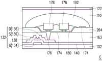
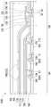
图1C为图1B的触控显示装置在虚线框C中以微发光二极管作为发光组件108的变化例的示意图。如图1C所示,各个微发光二极管178在此例如是微米等级尺寸的发光二极管晶片。微发光二极管178作为发光组件时,用以驱动微发光二极管178的薄膜晶体管132可以包括栅极G(例如由第一金属层134形成)、半导体层138、以及源极S和漏极D(例如由第二金属层136形成),其中半导体层138和栅极G以第一介电层140分隔开来,且第二绝缘层163覆盖此薄膜晶体管而可作为平坦层。在本实施例中,在第二绝缘层163上配置有介电层264,介电层264具有开口以定义出微发光二极管178的设置空间。也即,微发光二极管178可配置于介电层264的开口中。第三金属层174配置在第二绝缘层163上,位于介电层264的开口中,且微发光二极管178例如是接合在第三金属层174上。第三金属层174可通过贯穿第二绝缘层163的导接结构176与漏极D电性连接。此外,在微发光二极管178之间还填充有绝缘材料180。一对向导电层192设置于微发光二极管178上。本实施例的设计应用于图1B的触控显示装置时,第一绝缘层110与触控组件122则例如配置于对向导电层192上,其中第一绝缘层110与触控组件122仅示意性的表示于图1C中,而这些构件的具体设计可以参照前述内容。此外,第一绝缘层110可为单层式绝缘层,也可为多层式绝缘层。换言之,第一绝缘层110可不限定须采用有机层与无机层堆叠的结构,第一绝缘层110也可选择以单层无机层或是多层无机层来构成。FIG. 1C is a schematic diagram of a modification of the touch display device in FIG. 1B in which the micro-LED is used as the light-emitting
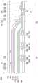
图2为本发明第一实施例的触控显示装置的变化例的剖面示意图。触控显示装置200与本发明第一实施例的触控显示装置100的差异在于触控组件122为底架桥结构,即:第二连接部153位于第一触控部148下方而相对较第一触控部148还接近于第一绝缘层110。而触控显示装置200的其余结构可参见上述第一实施例,从此不再赘述。2 is a schematic cross-sectional view of a modified example of the touch display device according to the first embodiment of the present invention. The difference between the
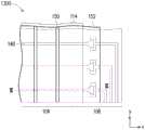
图3A为本发明第二实施例的触控显示装置的剖面示意图。图3A的触控显示装置300的基本结构与图1B的触控显示装置100的基本结构相同,除非另有说明,否则其具体描述可参见上述第一实施例。在触控显示装置300中,还可以包括贯穿第二绝缘层163的第二导接结构146以及第三传输部144。第三传输部144和第二导电层136可具有相同材料,而第二传输部128经由第二导接结构146与第三传输部144电性连接。3A is a schematic cross-sectional view of a touch display device according to a second embodiment of the present invention. The basic structure of the
在本实施例中,第三传输部144是由形成源极S和漏极D的第二导电层136形成的,所以第三传输部144与源极S和漏极D可在相同工艺中完成,可为相同层。另外,第二绝缘层163由第二导接结构146贯穿以使第二传输部128通过第二导接结构146连接至第三传输部144。此外,由图3A可知,第一导接结构130投影至基板102的区域A1和第二导接结构146投影至基板102的区域A2彼此分离不重叠。不过,在例如图3B的一实施例中,可选择利用栅极G的第一金属层134形成第三传输部144,而且第二导接结构146除了贯穿第二绝缘层163还贯穿介电层140与142。或是,在例如图3C的另一实施例中,可以还利用栅极G的第一金属层134形成第四传输部145,设置贯穿介电层140与142的第三导接结构155,并且使得由第二导电层136形成的第三传输部144通过第三导接结构155连接至第四传输部145。也就是说,触控信号传输线124可以包括由第一金属层134与第二金属层136至少一者所构成的传输部。In the present embodiment, the
依据一些实施例,第二传输部128与发光元件的第一电极109可为相同层,而且第三传输部144与第一金属层134或第二金属层136可为相同层,或者,在其他实施例中,第三传输部144与第二金属层136可为相同层,而且第四传输部145与第一金属层134可为相同层,如此,便不需要额外的过程制作金属线路来实现触控组件122的信号传输,可简化过程。According to some embodiments, the
依据一些实施例,作为触控信号传输的传输部,与发光组件的一电极或有源组件阵列的至少一导电层为相同层。如此,在完成发光组件的工艺之后,可不需额外制作金属线路来将触控组件的信号连接至外部,所以能避免额外制作金属线路对发光组件可能造成的伤害。依据一些实施例,由于触控组件中的第一触控部可通过触控信号传输线连接至由金属材料制作而成的第二传输部或第三传输部,故可提高触控信号的传递及回馈,提升触控的效能。According to some embodiments, as the transmission part for touch signal transmission, it is the same layer as an electrode of the light-emitting element or at least one conductive layer of the active element array. In this way, after the process of the light-emitting element is completed, there is no need to make additional metal lines to connect the signals of the touch element to the outside, so the possible damage to the light-emitting element caused by additionally making metal lines can be avoided. According to some embodiments, since the first touch part in the touch element can be connected to the second transmission part or the third transmission part made of a metal material through a touch signal transmission line, the transmission of touch signals and the transmission of touch signals can be improved. Feedback to improve touch performance.
图4为本发明第二实施例的触控显示装置的变化例的剖面示意图。触控显示装置400与本发明第二实施例的触控显示装置300的差异在于触控组件122为底架桥结构,即:第二连接部153位于第一触控部148下方。而触控显示装置400的其余结构可参见上述第二实施例,从此不再赘述。4 is a schematic cross-sectional view of a modified example of the touch display device according to the second embodiment of the present invention. The difference between the
图5为本发明第三实施例的触控显示装置的剖面示意图。图5的触控显示装置500的基本结构与图3A的触控显示装置300的基本结构相同,除非另有说明,否则其具体描述可参见上述实施例。在触控显示装置500中,第一导接结构130投影至基板102的区域A1和第二导接结构146投影至基板102的区域A2部分地重叠。5 is a schematic cross-sectional view of a touch display device according to a third embodiment of the present invention. The basic structure of the
图6为本发明第三实施例的触控显示装置的变化例的剖面示意图。触控显示装置600与本发明第三实施例的触控显示装置500的差异在于触控组件122为底架桥结构,即:第二连接部153位于第一触控部148下方。而触控显示装置600的其余结构可参见上述第三实施例,从此不再赘述。6 is a schematic cross-sectional view of a modification of the touch display device according to the third embodiment of the present invention. The difference between the
图7为本发明第四实施例的触控显示装置的剖面示意图。图7的触控显示装置700的基本结构与图3A的触控显示装置300的基本结构相同,除非另有说明,否则其具体描述可参见上述第二实施例。在触控显示装置700中,第一传输部126与所述第二连接部153为相同层,而与第一触控部148为不同层。详细而言,第一传输部126是和多个架桥(第二连接部153)使用相同材料以相同过程一起形成的。例如,第一传输部126和第二连接部153具有相同材料。因为图7的触控组件122例如是顶架桥结构,所以第一传输部126的一部分可叠置于第一触控部148上,以电性连接于第一触控部148。依据一些实施例,可以相同材料在同一道过程同时形成第二连接部153、第一传输部126和第一导接结构130。例如,第二连接部153、第一传输部126和第一导接结构130可具有相同材料,可为相同层。7 is a schematic cross-sectional view of a touch display device according to a fourth embodiment of the present invention. The basic structure of the
图8为本发明第四实施例的触控显示装置的变化例的剖面示意图。触控显示装置800与本发明第四实施例的触控显示装置700的差异在于触控组件122为底架桥结构,即:第二连接部153位于第一触控部148下方。因此,第一触控部148的一部分叠置于第一传输部126上,以电性连接第一传输部126。对于触控显示装置800的其余结构可参见上述第四实施例,从此不再赘述。8 is a schematic cross-sectional view of a modified example of the touch display device according to the fourth embodiment of the present invention. The difference between the
图9为本发明第五实施例的触控显示装置的剖面示意图。图9的触控显示装置900的基本结构与图3A的触控显示装置300的基本结构相同,除非另有说明,否则其具体描述可参见上述第二实施例。在触控显示装置900中,触控信号传输线124还包括辅助传输线部154,辅助传输线部154与第一传输部126叠置,且辅助传输线部154与第二连接部153为相同层,具有相同材料。通过在第一传输部126上叠置辅助传输线部154,不仅可进一步降低触控信号传输线124的整体阻抗,还可辅助修补第一传输部126有可能的断线部分,兼具改善工艺良率和提升触控效能的作用。9 is a schematic cross-sectional view of a touch display device according to a fifth embodiment of the present invention. The basic structure of the
图10为本发明第五实施例的触控显示装置的变化例的剖面示意图。图10的触控显示装置1000与图9的触控显示装置900的主要差异在于触控组件122为底架桥结构(即:第二连接部153位于第一触控部148下方),且第一传输部126与第二连接部153为相同层。而为使本领域技术人员容易了解本发明第五实施例的触控显示装置1000的基本结构,此处对于触控显示装置1000的具体描述可参照图8的触控显示装置800,除非另有说明,否则不再赘述。在触控显示装置1000中,是以相同工艺形成多个架桥(第二连接部153)和第一传输部126后才形成有第一触控部148,故而第一触控部148是堆叠于第一传输部126上,且覆盖第一传输部126。10 is a schematic cross-sectional view of a modified example of the touch display device according to the fifth embodiment of the present invention. The main difference between the
图11A为本发明第六实施例的触控显示装置的局部上视示意图。图11B为图11A的触控显示装置沿线II-II的剖面示意图。请同时参看图11A和图11B。触控显示装置1100的基本结构与图1B的触控显示装置100的基本结构相同,除非另有说明,否则其具体描述可参见上述第一实施例。在触控显示装置1100中,第一传输部126与第二连接部153为相同层。详细而言,第一传输部126是和多个架桥(第二连接部153)一起形成的,可具有相同材料。因为本发明的第六实施例的触控组件122例如是顶架桥结构,所以第一传输部126的一部分叠置于第一触控部148上,以电性连接第一触控部148。此外,在本实施例中,第一传输部126可直接作为触控信号传输线124且延伸至末段。第一传输部126可经由一接合部158而与一处理单元10电性连接以进行信号传输。11A is a schematic partial top view of a touch display device according to a sixth embodiment of the present invention. FIG. 11B is a schematic cross-sectional view of the touch display device of FIG. 11A along line II-II. Please refer to FIG. 11A and FIG. 11B simultaneously. The basic structure of the
在本实施例中,触控显示装置的触控型式为互容式,第一触控部148可为驱动电极,用以接收驱动信号,第二触控部150可为感测电极,用以将感测信号回传到处理单元。或者,第一触控部148可为感测电极,第二触控部150可为驱动电极。在其他实施例中,触控显示装置的触控型式也可为自容式。In this embodiment, the touch type of the touch display device is a mutual capacitance type, the
图11C为本发明第六实施例的触控显示装置的变化例的剖面示意图。触控显示装置1100’与触控显示装置1100的差异在于触控组件122为底架桥结构,即:第二连接部153位于第一触控部148下方。因此,第一触控部148的一部分叠置于第一传输部126上,以电性连接第一传输部126,第一传输部126可直接作为触控信号传输线124且延伸至末段,并具有接合部158。而触控显示装置1100’的其余结构可参见上述触控显示装置1100,从此不再赘述。11C is a schematic cross-sectional view of a modified example of the touch display device according to the sixth embodiment of the present invention. The difference between the
图12A为图11B的触控显示装置的变化例的剖面示意图。在图12A的触控显示装置1200中还包括以第二导电层136来形成第二传输部128,且第二传输部128的末端可具有接合部158。也就是说,第二传输部128是与源极S、漏极D在同一道工艺中制作而成。在此,第一导接结构130除了贯穿第一无机层112与第二无机层116外还可以贯穿第二绝缘层163以使第一传输部126连接至第二传输部128。图12A的触控显示装置1200的基本结构与触控显示装置1100的基本结构相同,除非另有说明,否则其具体描述可参见上述触控显示装置1100。FIG. 12A is a schematic cross-sectional view of a modification of the touch display device of FIG. 11B . In the
图12B为图11C的触控显示装置的变化例的剖面示意图。图12B的触控显示装置1200’与图12A的触控显示装置1200的差异在于触控组件122为底架桥结构,即:第二连接部153位于第一触控部148下方。和图11C比较,在图12B的触控显示装置1200’中还包括以第二导电层136来形成第二传输部128,且第二传输部128的末端可具有接合部158。也就是说,第二传输部128是与源极S、漏极D在同一道工艺中制作而成。在此,第一导接结构130除了贯穿第一无机层112与第二无机层116外还可以贯穿第二绝缘层163以使第一传输部126连接至第二传输部128。图12B的触控显示装置1200’的基本结构与触控显示装置1100’的基本结构相同,除非另有说明,否则其具体描述可参见上述触控显示装置1100’。FIG. 12B is a schematic cross-sectional view of a modified example of the touch display device of FIG. 11C . The difference between the
图13A为本发明第七实施例的触控显示装置的局部上视示意图。图13B为图13A的触控显示装置沿线III-III的剖面示意图。FIG. 13A is a schematic partial top view of a touch display device according to a seventh embodiment of the present invention. 13B is a schematic cross-sectional view of the touch display device of FIG. 13A along line III-III.
请同时参看图13A和图13B。图13A和图13B的触控显示装置1300的基本结构与图5的触控显示装置500的基本结构相同,除非另有说明,否则其具体描述可参见上述第三实施例。在图13A的触控显示装置1300中,示例性地示出几个层别而未示出全部的层别;而在图13B的触控显示装置1300中,省略薄膜晶体管132的完整结构,而仅绘出薄膜晶体管层3000作为代表,薄膜晶体管132的其余结构可参见上述实施例。在本实施例中,触控组件122例如是双层氧化铟锡结构(double indium tin oxide,DITO)。一第四绝缘层254,设置于第一触控部148和第二触控部150之间。第一触控部148例如是沿着第一方向x延伸,第二触控部150例如是沿着第二方向y延伸,第一方向x和第二方向y不同(第一方向x和第二方向y例如为彼此正交,但也可以采用非正交方式相交)。触控显示装置1300可包括多数个第一触控部148和多数个第二触控部150。多数个第一触控部148沿着第二方向y排列,多数个第二触控部150沿着第一方向x排列。在本实施例中,触控显示装置的触控型式为互容式,第一触控部148可为驱动电极,用以接收驱动信号,第二触控部150可为感测电极,用以将感测信号回传到处理单元。或者,第一触控部148可为感测电极,第二触控部150可为驱动电极。Please refer to FIG. 13A and FIG. 13B simultaneously. The basic structure of the
在本发明的第七实施例中,第一无机层112和第二无机层116在第一导接结构130远离显示区104的一侧具有倾斜状(taper)的边缘,而第一无机层112和第二无机层116部分覆盖在第二传输部128上并且顺应着第二传输部128的厚度而起伏,如此配置于第二无机层116上的第一传输部126可具有对应于第二传输部128的凸起表面。In the seventh embodiment of the present invention, the first
图14为本发明第七实施例的触控显示装置的变化例的剖面示意图。触控显示装置1400与本发明第七实施例的触控显示装置1300的差异在于第一无机层112的厚度和第二传输部128的厚度大致相等,且第一无机层112不与第二传输部128交叠,因此第一无机层112和第二传输部128构成大致平坦的表面,而第二无机层116部分覆盖在第二传输部128上。如此一来,由于第二无机层116无对应于第二传输部128的明显起伏,使得第一传输部126在有机层114的边缘之外的部分具有平坦表面。触控显示装置1400的其余结构可参见上述第七实施例,从此不再赘述。14 is a schematic cross-sectional view of a modification of the touch display device according to the seventh embodiment of the present invention. The difference between the
图15为本发明第七实施例的触控显示装置的另一变化例的剖面示意图。触控显示装置1500与本发明第七实施例的触控显示装置1300的差异在于第四绝缘层254未覆盖在第一传输部126上。而触控显示装置1500的其余结构可参见上述第七实施例,从此不再赘述。FIG. 15 is a schematic cross-sectional view of another modification of the touch display device according to the seventh embodiment of the present invention. The difference between the
图16A为本发明第八实施例的触控显示装置的局部上视示意图。图16B为图16A的触控显示装置沿线IV-IV的剖面示意图。16A is a schematic partial top view of a touch display device according to an eighth embodiment of the present invention. 16B is a schematic cross-sectional view of the touch display device of FIG. 16A along the line IV-IV.
请同时参看图16A和图16B。图16A和图16B的的触控显示装置1600的基本结构与图5的触控显示装置500的基本结构相同,除非另有说明,否则其具体描述可参见上述第三实施例。此外,在触控显示装置1600中,省略薄膜晶体管132的完整结构,而仅绘出薄膜晶体管层3000作为代表。在本实施例中,触控组件122例如是单层(one layer solution)形式的触控组件,即只包括第一触控部148的触控组件。并且,第一触控部148与发光层111交错设置,所以发光层111的上方没有覆盖第一触控部148。在本实施例中,触控显示装置的触控型式可为自容式,第一触控部148可接收一驱动信号并将一感测信号回传到处理单元。Please refer to FIG. 16A and FIG. 16B simultaneously. The basic structure of the
图17为本发明第八实施例的触控显示装置的变化例的剖面示意图。触控显示装置1700与本发明第八实施例的触控显示装置1600的差异在于第一触控部148与发光层111交叠设置,即:发光层111的上方覆盖有第一触控部148。而触控显示装置1700的其余结构可参见上述第八实施例,从此不再赘述。17 is a schematic cross-sectional view of a modification of the touch display device according to the eighth embodiment of the present invention. The difference between the
综上所述,本发明实施例的触控显示装置中,第一绝缘层设置于发光组件上,第一触控部和第一传输部设置于第一绝缘层上,第一传输部与第一触控部电性连接且与一处理单元电性连接以进行信号传输。依据一些实施例,周边区上的触控信号传输线的传输部,可与显示区上的触控部、导电层、或电极为相同层,而可简化过程。To sum up, in the touch display device according to the embodiment of the present invention, the first insulating layer is disposed on the light-emitting element, the first touch part and the first transmission part are disposed on the first insulating layer, and the first transmission part and the first transmission part are disposed on the first insulating layer. A touch portion is electrically connected to a processing unit for signal transmission. According to some embodiments, the transmission part of the touch signal transmission line on the peripheral area can be the same layer as the touch part, the conductive layer, or the electrode on the display area, which can simplify the process.
最后应说明的是:以上各实施例仅用以说明本发明的技术方案,而非对其限制;尽管参照前述各实施例对本发明进行了详细的说明,本领域的普通技术人员应当理解:其依然可以对前述各实施例所记载的技术方案进行修改,或者对其中部分或者全部技术特征进行等同替换;而这些修改或者替换,并不使相应技术方案的本质脱离本发明各实施例技术方案的范围。Finally, it should be noted that the above embodiments are only used to illustrate the technical solutions of the present invention, but not to limit them; although the present invention has been described in detail with reference to the foregoing embodiments, those of ordinary skill in the art should understand that: The technical solutions described in the foregoing embodiments can still be modified, or some or all of the technical features thereof can be equivalently replaced; and these modifications or replacements do not make the essence of the corresponding technical solutions deviate from the technical solutions of the embodiments of the present invention. scope.
Claims (9)
Translated fromChinesePriority Applications (10)
| Application Number | Priority Date | Filing Date | Title |
|---|---|---|---|
| CN201710019694.7ACN108304086B (en) | 2017-01-11 | 2017-01-11 | Touch control display device |
| CN202010825195.9ACN111966241B (en) | 2017-01-11 | 2017-01-11 | Touch display device |
| US15/846,239US10606391B2 (en) | 2017-01-11 | 2017-12-19 | Touch display device |
| KR1020180003652AKR102442395B1 (en) | 2017-01-11 | 2018-01-11 | Touch display device |
| US16/795,543US11144145B2 (en) | 2017-01-11 | 2020-02-19 | Touch display device |
| US17/465,857US11567596B2 (en) | 2017-01-11 | 2021-09-03 | Touch display device |
| KR1020220111959AKR102545431B1 (en) | 2017-01-11 | 2022-09-05 | Touch display device |
| US18/079,882US11907458B2 (en) | 2017-01-11 | 2022-12-13 | Sensing device |
| US18/414,482US20240184389A1 (en) | 2017-01-11 | 2024-01-17 | Electronic device |
| US19/008,534US20250147613A1 (en) | 2017-01-11 | 2025-01-02 | Electronic device |
Applications Claiming Priority (1)
| Application Number | Priority Date | Filing Date | Title |
|---|---|---|---|
| CN201710019694.7ACN108304086B (en) | 2017-01-11 | 2017-01-11 | Touch control display device |
Related Child Applications (1)
| Application Number | Title | Priority Date | Filing Date |
|---|---|---|---|
| CN202010825195.9ADivisionCN111966241B (en) | 2017-01-11 | 2017-01-11 | Touch display device |
Publications (2)
| Publication Number | Publication Date |
|---|---|
| CN108304086A CN108304086A (en) | 2018-07-20 |
| CN108304086Btrue CN108304086B (en) | 2020-09-15 |
Family
ID=62782375
Family Applications (2)
| Application Number | Title | Priority Date | Filing Date |
|---|---|---|---|
| CN201710019694.7AActiveCN108304086B (en) | 2017-01-11 | 2017-01-11 | Touch control display device |
| CN202010825195.9AActiveCN111966241B (en) | 2017-01-11 | 2017-01-11 | Touch display device |
Family Applications After (1)
| Application Number | Title | Priority Date | Filing Date |
|---|---|---|---|
| CN202010825195.9AActiveCN111966241B (en) | 2017-01-11 | 2017-01-11 | Touch display device |
Country Status (3)
| Country | Link |
|---|---|
| US (6) | US10606391B2 (en) |
| KR (2) | KR102442395B1 (en) |
| CN (2) | CN108304086B (en) |
Families Citing this family (13)
| Publication number | Priority date | Publication date | Assignee | Title |
|---|---|---|---|---|
| CN108304086B (en)* | 2017-01-11 | 2020-09-15 | 群创光电股份有限公司 | Touch control display device |
| KR102593459B1 (en)* | 2018-04-18 | 2023-10-24 | 엘지디스플레이 주식회사 | Organic light emitting display device with touch sensor |
| KR102528266B1 (en) | 2018-11-16 | 2023-05-04 | 삼성디스플레이 주식회사 | Electronic apparatus |
| KR102562807B1 (en) | 2018-11-23 | 2023-08-03 | 삼성디스플레이 주식회사 | Electronic apparatus |
| US10950809B2 (en)* | 2018-12-21 | 2021-03-16 | Wuhan China Star Optoelectronics Semiconductor Display Technology Co., Ltd. | Flexible display panel having a photoresist supporting element |
| CN109830521B (en)* | 2019-03-29 | 2021-03-16 | 武汉天马微电子有限公司 | Organic light-emitting display panel and display device |
| CN110286795B (en)* | 2019-06-27 | 2022-11-22 | 业成科技(成都)有限公司 | Touch control device |
| CN111142714B (en)* | 2020-01-21 | 2021-12-28 | 昆山国显光电有限公司 | Display panel and display device |
| CN111326565B (en)* | 2020-04-10 | 2022-11-15 | 云谷(固安)科技有限公司 | Display panel, manufacturing method thereof and display device |
| KR20210145026A (en)* | 2020-05-22 | 2021-12-01 | 삼성디스플레이 주식회사 | Electronic device |
| US11640210B2 (en)* | 2020-11-27 | 2023-05-02 | Tpk Advanced Solutions Inc. | Touch panel and touch device |
| WO2023142014A1 (en)* | 2022-01-29 | 2023-08-03 | 京东方科技集团股份有限公司 | Touch display panel, touch display device, and touch display motherboard |
| US20240353962A1 (en)* | 2022-04-28 | 2024-10-24 | Chengdu Boe Optoelectronics Technology Co., Ltd. | Display panel and display device |
Citations (4)
| Publication number | Priority date | Publication date | Assignee | Title |
|---|---|---|---|---|
| CN105549242A (en)* | 2014-10-22 | 2016-05-04 | 三星显示有限公司 | Liquid crystal display |
| CN105655378A (en)* | 2016-01-04 | 2016-06-08 | 京东方科技集团股份有限公司 | Array substrate, OLED display panel, manufacturing method and display device |
| CN105824457A (en)* | 2015-01-28 | 2016-08-03 | 三星显示有限公司 | Organic light emitting diode display |
| CN105912165A (en)* | 2016-02-26 | 2016-08-31 | 友达光电股份有限公司 | Organic light emitting display device |
Family Cites Families (30)
| Publication number | Priority date | Publication date | Assignee | Title |
|---|---|---|---|---|
| US8217396B2 (en)* | 2004-07-30 | 2012-07-10 | Semiconductor Energy Laboratory Co., Ltd. | Display device comprising electrode layer contacting wiring in the connection region and extending to pixel region |
| EP1793266B1 (en) | 2005-12-05 | 2017-03-08 | Semiconductor Energy Laboratory Co., Ltd. | Transflective Liquid Crystal Display with a Horizontal Electric Field Configuration |
| JP5400904B2 (en)* | 2011-07-15 | 2014-01-29 | アルプス電気株式会社 | Manufacturing method of touch panel integrated display device |
| KR20140012803A (en)* | 2012-07-23 | 2014-02-04 | 삼성디스플레이 주식회사 | Display panel and method of driving the same |
| KR20150033468A (en)* | 2013-09-24 | 2015-04-01 | 엘지이노텍 주식회사 | Touch panel |
| CN104571655B (en)* | 2013-10-15 | 2017-09-15 | 鸿富锦精密工业(深圳)有限公司 | touch display device |
| KR102187911B1 (en)* | 2013-11-13 | 2020-12-07 | 엘지이노텍 주식회사 | Touch panel |
| KR102144084B1 (en)* | 2013-11-19 | 2020-08-14 | 삼성디스플레이 주식회사 | display device integrated touch screen panel |
| KR102192035B1 (en) | 2013-12-02 | 2020-12-17 | 삼성디스플레이 주식회사 | Flexible display device including touch detecting sensor |
| KR102162912B1 (en)* | 2013-12-06 | 2020-10-07 | 엘지디스플레이 주식회사 | Organic electroluminescent device having touch panel and method for fabricating the same |
| KR102302811B1 (en)* | 2013-12-16 | 2021-09-16 | 엘지이노텍 주식회사 | Touch panel |
| KR102276330B1 (en) | 2014-03-10 | 2021-07-13 | 엘지디스플레이 주식회사 | Display device and method of drving the same |
| CN104123054B (en)* | 2014-07-22 | 2017-10-20 | 昆山龙腾光电有限公司 | Touch control display apparatus |
| US9891769B2 (en)* | 2014-11-25 | 2018-02-13 | Lg Innotek Co., Ltd. | Touch window |
| KR102289934B1 (en)* | 2014-11-28 | 2021-08-13 | 삼성디스플레이 주식회사 | Display device including touch detecting sensor |
| US9535522B2 (en)* | 2014-12-22 | 2017-01-03 | Lg Display Co., Ltd. | Flexible organic light emitting diode display device |
| US9508681B2 (en)* | 2014-12-22 | 2016-11-29 | Google Inc. | Stacked semiconductor chip RGBZ sensor |
| KR102312260B1 (en)* | 2015-01-09 | 2021-10-13 | 삼성디스플레이 주식회사 | Flexible touch panel and flexible display device |
| CN104777637B (en)* | 2015-05-08 | 2018-01-02 | 上海中航光电子有限公司 | Array base palte, touch control display apparatus and its method of testing |
| TWI581149B (en)* | 2015-11-02 | 2017-05-01 | 友達光電股份有限公司 | Touch display panel |
| CN105810716A (en)* | 2016-04-01 | 2016-07-27 | 友达光电股份有限公司 | Flexible display device and preparation method |
| KR102066099B1 (en)* | 2016-07-29 | 2020-01-14 | 엘지디스플레이 주식회사 | Organic light emitting display and fabricating method thereof |
| KR102601207B1 (en)* | 2016-07-29 | 2023-11-13 | 삼성디스플레이 주식회사 | Display device |
| US10430000B2 (en)* | 2016-08-05 | 2019-10-01 | Innolux Corporation | Touch display device |
| KR102648415B1 (en)* | 2016-11-30 | 2024-03-18 | 엘지디스플레이 주식회사 | Touch Screen Integrated Display Device and Method for Manufacturing the Same |
| KR102670360B1 (en)* | 2016-12-08 | 2024-05-28 | 엘지디스플레이 주식회사 | Display device with integrated touch screen and method for fabricating the same |
| KR102793060B1 (en)* | 2016-12-16 | 2025-04-08 | 엘지디스플레이 주식회사 | Display device and fabricating method thereof |
| KR102810070B1 (en)* | 2016-12-27 | 2025-05-21 | 엘지디스플레이 주식회사 | Display device |
| KR20180076689A (en)* | 2016-12-28 | 2018-07-06 | 엘지디스플레이 주식회사 | Display device |
| CN108304086B (en)* | 2017-01-11 | 2020-09-15 | 群创光电股份有限公司 | Touch control display device |
- 2017
- 2017-01-11CNCN201710019694.7Apatent/CN108304086B/enactiveActive
- 2017-01-11CNCN202010825195.9Apatent/CN111966241B/enactiveActive
- 2017-12-19USUS15/846,239patent/US10606391B2/enactiveActive
- 2018
- 2018-01-11KRKR1020180003652Apatent/KR102442395B1/enactiveActive
- 2020
- 2020-02-19USUS16/795,543patent/US11144145B2/enactiveActive
- 2021
- 2021-09-03USUS17/465,857patent/US11567596B2/enactiveActive
- 2022
- 2022-09-05KRKR1020220111959Apatent/KR102545431B1/enactiveActive
- 2022-12-13USUS18/079,882patent/US11907458B2/enactiveActive
- 2024
- 2024-01-17USUS18/414,482patent/US20240184389A1/enactivePending
- 2025
- 2025-01-02USUS19/008,534patent/US20250147613A1/enactivePending
Patent Citations (4)
| Publication number | Priority date | Publication date | Assignee | Title |
|---|---|---|---|---|
| CN105549242A (en)* | 2014-10-22 | 2016-05-04 | 三星显示有限公司 | Liquid crystal display |
| CN105824457A (en)* | 2015-01-28 | 2016-08-03 | 三星显示有限公司 | Organic light emitting diode display |
| CN105655378A (en)* | 2016-01-04 | 2016-06-08 | 京东方科技集团股份有限公司 | Array substrate, OLED display panel, manufacturing method and display device |
| CN105912165A (en)* | 2016-02-26 | 2016-08-31 | 友达光电股份有限公司 | Organic light emitting display device |
Also Published As
| Publication number | Publication date |
|---|---|
| KR20220126285A (en) | 2022-09-15 |
| US20250147613A1 (en) | 2025-05-08 |
| US11907458B2 (en) | 2024-02-20 |
| US20200192512A1 (en) | 2020-06-18 |
| CN111966241B (en) | 2023-05-30 |
| US20240184389A1 (en) | 2024-06-06 |
| KR102442395B1 (en) | 2022-09-08 |
| US10606391B2 (en) | 2020-03-31 |
| KR20180082976A (en) | 2018-07-19 |
| US20210397287A1 (en) | 2021-12-23 |
| CN111966241A (en) | 2020-11-20 |
| US11144145B2 (en) | 2021-10-12 |
| US20230111761A1 (en) | 2023-04-13 |
| CN108304086A (en) | 2018-07-20 |
| US20180196564A1 (en) | 2018-07-12 |
| KR102545431B1 (en) | 2023-06-20 |
| US11567596B2 (en) | 2023-01-31 |
Similar Documents
| Publication | Publication Date | Title |
|---|---|---|
| CN108304086B (en) | Touch control display device | |
| CN103943061B (en) | OLED display device with built-in touch structure | |
| CN109524435B (en) | display device | |
| CN105390526B (en) | It is integrated with the flexible oganic light-emitting display device of In-cell touch panel | |
| KR102124906B1 (en) | Organic electro luminescent device having touch screen and method of fabricationg the same | |
| CN111785757B (en) | Display device, display panel and manufacturing method thereof | |
| CN106125424B (en) | A kind of array substrate, display panel and display device | |
| CN113126806A (en) | Touch display device | |
| CN108987426B (en) | Flexible LED display panel and electronic equipment | |
| CN107272942A (en) | Touch-screen and the display device with it | |
| CN115172436B (en) | Display panel and display device | |
| WO2020118845A1 (en) | Touch display panel and manufacturing method therefor, and touch display device | |
| CN104064567B (en) | Array substrate, display device and manufacturing method of array substrate | |
| CN105224117B (en) | Touching display screen and its manufacturing method | |
| CN102569341A (en) | Organic light emitting diode display | |
| CN112015299B (en) | Touch substrate and touch device | |
| CN112631452B (en) | Pressure sensor and display device including the same | |
| CN113540180A (en) | Display device | |
| TWM522419U (en) | Fingerprint recognition sensor | |
| KR102521628B1 (en) | Display apparatus | |
| KR20230094458A (en) | Transparent display device with touch sensor | |
| CN108091676B (en) | A touch display substrate, a manufacturing method thereof, and a touch display device | |
| KR102510942B1 (en) | Organic light emitting display device | |
| WO2021184435A1 (en) | Touch display device and method for manufacturing touch display device | |
| CN115241247A (en) | a display panel |
Legal Events
| Date | Code | Title | Description |
|---|---|---|---|
| PB01 | Publication | ||
| PB01 | Publication | ||
| SE01 | Entry into force of request for substantive examination | ||
| SE01 | Entry into force of request for substantive examination | ||
| GR01 | Patent grant | ||
| GR01 | Patent grant |