CN108303377B - A thermo-optic effect optical waveguide detection device - Google Patents
A thermo-optic effect optical waveguide detection deviceDownload PDFInfo
- Publication number
- CN108303377B CN108303377BCN201810105858.2ACN201810105858ACN108303377BCN 108303377 BCN108303377 BCN 108303377BCN 201810105858 ACN201810105858 ACN 201810105858ACN 108303377 BCN108303377 BCN 108303377B
- Authority
- CN
- China
- Prior art keywords
- terminal
- coupled
- transistor
- control
- circuit
- Prior art date
- Legal status (The legal status is an assumption and is not a legal conclusion. Google has not performed a legal analysis and makes no representation as to the accuracy of the status listed.)
- Active
Links
- 230000003287optical effectEffects0.000titleclaimsabstractdescription119
- 238000001514detection methodMethods0.000titleclaimsabstractdescription46
- 230000000694effectsEffects0.000titleclaimsabstractdescription28
- 239000004065semiconductorSubstances0.000claimsabstractdescription15
- 238000010438heat treatmentMethods0.000claimsabstractdescription9
- VYPSYNLAJGMNEJ-UHFFFAOYSA-NSilicium dioxideChemical compoundO=[Si]=OVYPSYNLAJGMNEJ-UHFFFAOYSA-N0.000claimsdescription18
- 230000008859changeEffects0.000claimsdescription11
- 238000004364calculation methodMethods0.000claimsdescription9
- 239000000377silicon dioxideSubstances0.000claimsdescription9
- 238000009529body temperature measurementMethods0.000claimsdescription6
- 239000000758substrateSubstances0.000claimsdescription6
- 238000012360testing methodMethods0.000claimsdescription6
- 235000012239silicon dioxideNutrition0.000claimsdescription5
- XUIMIQQOPSSXEZ-UHFFFAOYSA-NSiliconChemical compound[Si]XUIMIQQOPSSXEZ-UHFFFAOYSA-N0.000claimsdescription4
- 229910052710siliconInorganic materials0.000claimsdescription4
- 239000010703siliconSubstances0.000claimsdescription4
- 238000005516engineering processMethods0.000abstractdescription4
- 239000007788liquidSubstances0.000description9
- 238000010586diagramMethods0.000description7
- 239000000126substanceSubstances0.000description5
- 230000036541healthEffects0.000description4
- 239000000463materialSubstances0.000description4
- 230000001629suppressionEffects0.000description4
- 238000004458analytical methodMethods0.000description3
- 201000010099diseaseDiseases0.000description3
- 208000037265diseases, disorders, signs and symptomsDiseases0.000description3
- 238000010339medical testMethods0.000description3
- 238000000034methodMethods0.000description3
- XLYOFNOQVPJJNP-UHFFFAOYSA-NwaterSubstancesOXLYOFNOQVPJJNP-UHFFFAOYSA-N0.000description3
- 238000006243chemical reactionMethods0.000description2
- 238000004590computer programMethods0.000description2
- 230000008878couplingEffects0.000description2
- 238000010168coupling processMethods0.000description2
- 238000005859coupling reactionMethods0.000description2
- 238000011161developmentMethods0.000description2
- 239000003814drugSubstances0.000description2
- 239000002184metalSubstances0.000description2
- 238000012123point-of-care testingMethods0.000description2
- 230000035945sensitivityEffects0.000description2
- 241000894006BacteriaSpecies0.000description1
- WQZGKKKJIJFFOK-GASJEMHNSA-NGlucoseNatural productsOC[C@H]1OC(O)[C@H](O)[C@@H](O)[C@@H]1OWQZGKKKJIJFFOK-GASJEMHNSA-N0.000description1
- 241000700605VirusesSpecies0.000description1
- 239000000427antigenSubstances0.000description1
- 230000000975bioactive effectEffects0.000description1
- 230000004071biological effectEffects0.000description1
- 239000003990capacitorSubstances0.000description1
- 230000002925chemical effectEffects0.000description1
- 230000007613environmental effectEffects0.000description1
- 239000003344environmental pollutantSubstances0.000description1
- 238000003912environmental pollutionMethods0.000description1
- 239000002778food additiveSubstances0.000description1
- 235000013373food additiveNutrition0.000description1
- 239000008103glucoseSubstances0.000description1
- 238000007689inspectionMethods0.000description1
- 239000007791liquid phaseSubstances0.000description1
- 230000007774longtermEffects0.000description1
- 238000012544monitoring processMethods0.000description1
- 230000000704physical effectEffects0.000description1
- 230000002265preventionEffects0.000description1
- 230000008569processEffects0.000description1
- 238000011896sensitive detectionMethods0.000description1
- 230000004083survival effectEffects0.000description1
Images


Classifications
- G—PHYSICS
- G01—MEASURING; TESTING
- G01N—INVESTIGATING OR ANALYSING MATERIALS BY DETERMINING THEIR CHEMICAL OR PHYSICAL PROPERTIES
- G01N21/00—Investigating or analysing materials by the use of optical means, i.e. using sub-millimetre waves, infrared, visible or ultraviolet light
- G01N21/17—Systems in which incident light is modified in accordance with the properties of the material investigated
- G01N21/171—Systems in which incident light is modified in accordance with the properties of the material investigated with calorimetric detection, e.g. with thermal lens detection
Landscapes
- Physics & Mathematics (AREA)
- Health & Medical Sciences (AREA)
- Life Sciences & Earth Sciences (AREA)
- Chemical & Material Sciences (AREA)
- Analytical Chemistry (AREA)
- Biochemistry (AREA)
- General Health & Medical Sciences (AREA)
- General Physics & Mathematics (AREA)
- Immunology (AREA)
- Pathology (AREA)
- Photometry And Measurement Of Optical Pulse Characteristics (AREA)
- Optical Modulation, Optical Deflection, Nonlinear Optics, Optical Demodulation, Optical Logic Elements (AREA)
Abstract
Translated fromChinese
Description
Translated fromChinese技术领域technical field
本发明涉及一种光电检测装置,特别涉及一种基于热光效应的光波导检测装置。The invention relates to a photoelectric detection device, in particular to an optical waveguide detection device based on thermo-optic effect.
背景技术Background technique
随着人类科学技术的巨大进步和经济、社会的不断发展,普通民众越来越注重个人的身体健康,对健康医疗提出了更高的要求。无论疾病的预防或治疗,都需要即刻、及时乃至长期大数据量的人体医学检测数据。但是,专业医学检测设备的稀缺、医疗检测价格的昂贵、专业检测场所的局限,都极大限制了普通民众在健康体检甚至疾病治疗时的医学检测。因此,以便捷低廉、灵敏快速为主要特征的“即刻检验”(Point-of-CareTesting,POCT)成为医疗设备的发展趋势之一。另一方面,在当今世界,环境污染、食品安全、恐怖袭击等问题也时时困扰着很多国家和地区,对人们的健康乃至生存造成了严重威胁。专业机构需要对环境污染物、食品添加剂、病毒细菌等目标进行现场快速检测(Rapidon-sitedetection),微型便携、操作简便、快速灵敏的检测分析设备也显得尤为重要。因此,便携便捷、低耗低廉、灵敏快速的生物学、化学检测分析手段是医学、环境、食品、反恐等多个社会领域的热点需求。With the great progress of human science and technology and the continuous development of economy and society, ordinary people pay more and more attention to personal health, and put forward higher requirements for health care. Regardless of the prevention or treatment of diseases, immediate, timely and even long-term large-scale human medical detection data are required. However, the scarcity of professional medical testing equipment, the high price of medical testing, and the limitations of professional testing sites have greatly restricted the medical testing of ordinary people during health checkups and even disease treatment. Therefore, "Point-of-Care Testing" (POCT), which is characterized by convenience, low cost, sensitivity and speed, has become one of the development trends of medical equipment. On the other hand, in today's world, problems such as environmental pollution, food safety, and terrorist attacks have plagued many countries and regions from time to time, posing serious threats to people's health and even survival. Professional institutions need rapid on-site detection (Rapidon-site detection) of environmental pollutants, food additives, viruses and bacteria, etc. Micro-portable, easy-to-operate, fast and sensitive detection and analysis equipment is also particularly important. Therefore, portable, convenient, low-cost, low-cost, sensitive and rapid biological and chemical detection and analysis methods are hot demands in many social fields such as medicine, environment, food, and anti-terrorism.
作为一种新兴的生物化学检测手段,光波导生化传感器以其无需标定、高灵敏度、结构简单、可实时实地检测等优良的性质,在食品安全、疾病检测、环境监测等方面已实现了多种的应用,具有非常光明的前景。由于折射率通常和液体的化学性质(如物质成分、各组分含量以及粘稠度等)联系在一起,另外,很多生物分子的折射率也是其结构、大小、形态等参数的函数。同时折射率是所有材料的固有特征,它通常不会受物理、化学和生物效应的影响而发生变化,所以通过折射率测量来实现对各种化学量的传感无疑是最简单和直接的途径。通常情况下在波导表面涂覆的高选择性敏感层与液体中的待测分子发生特异性反应,其引起导模的折射率变化由探测设备测得,即可反映出样品特性上的差异。利用折射率传感器测量气/液相浓度、监测生物活性膜厚度、抗体-抗原反应和DNA反应中参数的变化等,可以实现对生物化学、医学、生命科学等领域中各种现象的分析。As an emerging biochemical detection method, the optical waveguide biochemical sensor has achieved a variety of applications in food safety, disease detection, and environmental monitoring due to its excellent properties such as no need for calibration, high sensitivity, simple structure, and real-time on-site detection. application has a very bright future. Because the refractive index is usually associated with the chemical properties of the liquid (such as material composition, component content, and viscosity, etc.), in addition, the refractive index of many biomolecules is also a function of its structure, size, shape and other parameters. At the same time, the refractive index is an inherent feature of all materials, and it usually does not change under the influence of physical, chemical and biological effects, so it is undoubtedly the simplest and most direct way to realize the sensing of various chemical quantities by measuring the refractive index . Usually, the highly selective sensitive layer coated on the surface of the waveguide reacts specifically with the molecules to be measured in the liquid, and the refractive index change of the guided mode caused by it is measured by the detection equipment, which can reflect the difference in the characteristics of the sample. The use of refractive index sensors to measure gas/liquid phase concentrations, monitor bioactive film thickness, antibody-antigen reactions, and changes in parameters in DNA reactions can realize the analysis of various phenomena in the fields of biochemistry, medicine, and life sciences.
发明内容Contents of the invention
为解决上述问题,提供了一种一种热光效应光波导检测装置,包括:第一光电探测器,具有输入端、输出端,基于参考光源产生第一电信号;光波导器件,具有第一光输入端、第一光输出端、第一控制端和第二控制端,具有第一波导和第二波导,其第一光输入端用于接收第一光信号,其第一光输出端用于提供第一光输出信号,其第一控制端和第二控制端接收控制电压,基于热光效应调整光第一光输出信号;第二光电探测器,具有输入端、输出端,其输入端耦接至光波导器件的光输出端,基于第二光信号产生第二电信号;第一放大器,具有电源端、接地端、第一端、第二端和输出端,其电源端耦接至电源,其接地端耦接至地,其第一端耦接至第一光电检测器件输出端以接收第一电信号,其第二端耦接至第二光电检测器件输出端以接收第二电信号,其输出端耦接至所述光波导器件的第一控制端并提供第一模拟信号。In order to solve the above problems, a thermo-optic effect optical waveguide detection device is provided, including: a first photodetector, which has an input end and an output end, and generates a first electrical signal based on a reference light source; an optical waveguide device, which has a first The optical input terminal, the first optical output terminal, the first control terminal and the second control terminal have a first waveguide and a second waveguide, the first optical input terminal is used for receiving the first optical signal, and the first optical output terminal is used for For providing the first light output signal, its first control terminal and second control terminal receive the control voltage, and adjust the light first light output signal based on the thermo-optic effect; the second photodetector has an input terminal and an output terminal, and its input terminal Coupled to the optical output terminal of the optical waveguide device, based on the second optical signal to generate a second electrical signal; the first amplifier has a power supply terminal, a ground terminal, a first terminal, a second terminal and an output terminal, and its power supply terminal is coupled to The power supply, whose ground terminal is coupled to the ground, whose first terminal is coupled to the output terminal of the first photodetection device to receive the first electrical signal, and whose second terminal is coupled to the output terminal of the second photodetection device to receive the second electrical signal signal, the output end of which is coupled to the first control end of the optical waveguide device and provides a first analog signal.
可以采用现存半导体工艺将光波导、加热装置、温度检测装置、放大器等全部集成于单个晶片(例如硅片)上。第一放大器输出的电信号调整光波导器件的温度,基于热光效应调整光波导器件的输出光信号,从而获得环路稳定。测量第一放大器输出的电信号或者光波导器件的温度即可快速准确地获得待测物品的信息。The optical waveguide, heating device, temperature detection device, amplifier, etc. can all be integrated on a single chip (such as a silicon chip) by using existing semiconductor technology. The electrical signal output by the first amplifier adjusts the temperature of the optical waveguide device, and adjusts the output optical signal of the optical waveguide device based on the thermo-optic effect, thereby obtaining loop stability. By measuring the electrical signal output by the first amplifier or the temperature of the optical waveguide device, the information of the object to be tested can be obtained quickly and accurately.
附图说明Description of drawings
图1示出根据本发明一个实施例的热光效应光波导检测装置10。FIG. 1 shows a thermo-optic effect optical
图2示出根据本发明一个实施例的光波导器件20的结构示意图。FIG. 2 shows a schematic structural diagram of an
图2(a)为波导器件三维立体示意图。Fig. 2(a) is a three-dimensional schematic diagram of the waveguide device.
图2(b)为波导器件截面图。Figure 2(b) is a cross-sectional view of the waveguide device.
图2(c)为波导器件俯视图。Figure 2(c) is a top view of the waveguide device.
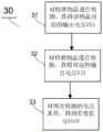
图3示出根据本发明一个实施例的检测流程图30。FIG. 3 shows a
图4为根据本发明一个实施例的偏置和温测电路40的示意图。FIG. 4 is a schematic diagram of a biasing and
图5为根据本发明一个实施例的偏置和温测电路50的电路图。FIG. 5 is a circuit diagram of a bias and
图6示出根据本发明一个实施例的光波导器件60。FIG. 6 shows an
图6(a)为光波导器件三维立体示意图。Fig. 6(a) is a three-dimensional schematic diagram of an optical waveguide device.
图6(b)为光波导器件切面图。Figure 6(b) is a cross-sectional view of the optical waveguide device.
图6(C)为图6(a)中光波导器件沿XY面的切面图。FIG. 6(C) is a sectional view of the optical waveguide device in FIG. 6(a) along the XY plane.
图7示出根据本发明一个实施例的热光效应光波导检测装置70。FIG. 7 shows a thermo-optic effect optical
具体实施方式Detailed ways
在下文所述的特定实施例代表本发明的示例性实施例,并且本质上仅为示例说明而非限制。在说明书中,提及“一个实施例”或者“实施例”意味着结合该实施例所描述的特定特征、结构或者特性包括在本发明的至少一个实施例中。术语“在一个实施例中”在说明书中各个位置出现并不全部涉及相同的实施例,也不是相互排除其他实施例或者可变实施例。本说明书中公开的所有特征,或公开的所有方法或过程中的步骤,除了互相排斥的特征和/或步骤以外,均可以以任何方式组合。The specific embodiments described below represent exemplary embodiments of the invention and are merely illustrative rather than limiting in nature. In the specification, reference to "one embodiment" or "an embodiment" means that a particular feature, structure, or characteristic described in connection with the embodiment is included in at least one embodiment of the present invention. The appearances of the term "in one embodiment" in various places in the specification are not all referring to the same embodiment, nor are they intended to mutually exclude other or alternative embodiments. All features disclosed in this specification, or steps in all methods or processes disclosed, may be combined in any manner, except for mutually exclusive features and/or steps.
下面将参考附图详细说明本发明的具体实施方式。贯穿所有附图相同的附图标记表示相同的部件或特征。Specific embodiments of the present invention will be described in detail below with reference to the accompanying drawings. Like reference numerals refer to like parts or features throughout the drawings.
图1是根据本发明一个实施例的光电检测装置10,该装置包括第一光电探测器11、光波导器件12、第二光电探测器13和第一放大器14。FIG. 1 is a
第一光电探测器11,具有输入端和输出端,基于参考光源PREF产生第一电信号V1。The
光波导器件12,具有第一光输入端、第一光输出端、第一控制端和第二控制端,其第一光输入端用于接收第一光信号PIN,其第一光输出端用于提供第一光输出信号POUT1,其第二控制端耦接至地电势GND。第一控制端和第二控制端接收外部控制信号以调整光波导器件的温度,基于热光效应改变光波导器件的折射率,进而调整第一光输出信号POUT1。The
第二光电探测器13,具有输入端、输出端,其输入端耦接至光波导器件102的第一光输出端,基于第一光输出信号POUT1产生第二电信号V2。The
第一放大器14,具有电源端、接地端、第一端、第二端和输出端,其电源端耦接至内部电源VINT,其接地端耦接至地电势GND,其第一端耦接至第一光电检测器件11输出端以接收第一电信号V1,其第二端耦接至第二光电探测器件13输出端以接收第二电信号V2,其输出端耦接至所述光波导器件12的第一控制端并提供第一模拟信号VA1。The
当待检测物品放置进入光波导器件12的检测区域后,由于折射率的改变(待测物品的折射率不同于空气或水),光波导器件12输出的光信号(即第一光输出信号POUT1)将会发生变化,第二光电探测器13输出的第二电信号V2发生变化,第一放大器14输出电压发生变化,光波导器件的控制电压(第一模拟信号VA1)调整光波导器件12的温度,由于热光效应改变光波导器件12的折射率从而改变第二光电探测器13的输入信号(第一光输出信号POUT1)和输出信号(第二电信号V2),使得第一电信号V1等于第二电信号V2。不同的物体、不同的化学性质、或不同的浓度具有不同的折射率,第一放大器14也会输出不同电压。测量第一模拟信号VA1的电压就可以获得物品信息,例如浓度、粘稠度、物质属性等。When the object to be detected is placed into the detection area of the
图2示出根据本发明一个实施例的光波导器件20的结构示意图,其中2(a)为三维立体示意图,2(b)为截面图,2(c)为俯视图,光波导器件20可以作为光波导器件12用于检测装置10。需要指出的是光波导器件20仅是一个实施例而非限制,本领域的技术人员可以根据本发明的教导选择其他热光效应光波导器件/热光效应定向耦合器作为光波导器件12用于检测装置10。在一个实施例中,热光效应指通过控制电压改变光波导器件温度,从而改变导光特性,例如折射率、光波导之间的耦合等,最终改变光强。Fig. 2 shows a schematic structural view of an
如图2(a)所示,光波导器件20包括衬底层21,一般采用Si材料;两条平行的光波导22和23,一般采用二氧化硅,集成在硅衬底21的上表面24上方;作为电极用于连接外部(控制)电压的接触孔25-28。图2(b)示出光波导器件20沿YZ平面的切面图(如2(a)中虚线/切线所示)。波导层22和23的下方采用半导体工艺集成了电阻器221和231作为加热装置。电阻器通过金属线或者重掺杂半导体区域连接至外部控制信号或进行互联。图2(c)示出光波导20的俯视图,两条平行的光波导22和23集成在半导体层21上。第一光信号PIN通过第一光输入端进入光波导22后,一部分通过光波导22的输出端产生第二光输出信号POUT2,另外一分部被耦合至光波导23并在其输出端提供第一光输出信号POUT1。合理设置光波导的宽度(d1)和光波导耦合距离(d2),光波导器件20可以作为理想的定向耦合器使用,即,第一光信号PIN全部被耦合至光波导23并在其输出端提供第一光输出信号POUT1(PIN实质等于POUT1,POUT2实质等于0)。As shown in Figure 2(a), the
根据本发明的一个实施例,电阻器221第一端通过接触孔27接收第一模拟信号VA1,电阻器221第二端通过接触孔28连接至接地端;电阻器231第一端通过接触孔26接收第一模拟信号VA1,电阻器231第二端通过接触孔25连接至接地端。通电后,电阻器221和231即可分别对光波导22和23进行加热。在其他实施例中,电阻器221和231还可以组成串联电阻对光波导22和23进行加热。光波导22和23之间的区域用以盛放待测物体/液体,称为测试区29。当待测液体进入测试区29后,由于待测液体的折射率高于空气或水的折射率,导致耦合进入光波导23的光量发生变化,进而使得第二电信号V2发生变化,第一放大器V1提供的VA1也发生变化,进而调整光波导器件的温度,由于热光效应,改变光波导的折射率,使得光信号PIN再次耦合进入光波导23,以最终达到平衡。不同的液体具有不同的折射率,导致VA1发生不同变化,即VA1的电压包含了待测液体折射率信息。According to an embodiment of the present invention, the first end of the
需要指出的是,加热装置不仅限于集成电阻,还可以是金属电阻,还可以是电阻和MOS管串联或其他。电阻221和231不限于集成于波导层下面,还可以是侧面或上面。It should be pointed out that the heating device is not limited to integrated resistors, but can also be metal resistors, resistors connected in series with MOS tubes, or others. The
由于两个光电探测器之间不可避免的存在失配,误差放大器14也存在失调,因而将同一种液体放置在两个不同的检测装置时,第一放大器可能会得到两个不同的输出电压。为解决上述问题,可以采用图3所示检测方法。Due to the unavoidable mismatch between the two photodetectors, the
首先,执行步骤31,对校准物品进行检测,获得该物品对应的输出电压VS1。而后,执行步骤32,对待测物品进行检测,获得对应的输出电压VJ1。最后,执行步骤33,对两次检测的电压求差,得到差值信号(VDIF=VS1-VJ1)。由于两次检测所得的电压都包含了光电探测器失配值、第一放大器的失调电压等因素。相减所得差值就去除了失调、失配的影响,仅包含了校准物品的折射率信息和待测物品的折射率信息,从而提高了精准度。优选地,校准物品可以是纯水、特定浓度葡萄糖或者空气。First, step 31 is executed to detect the calibration item and obtain the output voltage VS1 corresponding to the item. Then, step 32 is executed to detect the object to be tested and obtain the corresponding output voltage VJ1. Finally, step 33 is executed to obtain the difference between the two detected voltages to obtain a difference signal (VDIF=VS1-VJ1). The voltages obtained from the two detections include factors such as the mismatch value of the photodetector, the offset voltage of the first amplifier, and the like. The difference obtained by subtraction removes the influence of misalignment and mismatch, and only includes the refractive index information of the calibration item and the refractive index information of the item to be measured, thereby improving the accuracy. Preferably, the calibration item can be pure water, glucose with a specific concentration or air.
由于电子电路中存储模拟电压或者计算两个模拟电压之间的差值不仅困难而且精度低,优选地,检测电路10还可以进一步包括AD转换器15,寄存器16、计算单元17和查找表18。Since storing analog voltages in electronic circuits or calculating the difference between two analog voltages is difficult and has low precision, preferably, the
AD转换器15,用于将第一模拟信号VA1转换为第一数字信号D1。第一寄存器(RegisterUnit)16,具有控制端、输入端和输出端,其输入端用以接收所述第一数字信号D1,其输出端提供第二数字信号D2。第一计算单元(ComputingUnit)17,具有第一输入端、第二输入端和输出端,其第一输入端耦接至所述寄存器16输出端以接收所述第二数字信号D2,其第二端耦接至所述AD转换器15输出端用以接收第一数字信号D1,其输出端提供计算信号。查找表,基于计算信号和预存储数据输出待测物品信息。The
在一个实施例中,对校准物品进行检测,该物品对应的第一数字信号即存储进入第一寄存器16。对物品进行检查时,第一计算单元17将该待测物品对应的数字信号与寄存器存储的校准电压(校准数字信号)进行运算(例如相减),并将结果提供给查找表18。查找表根据与存储信息输出物品信息,例如在一个实施例中,差值信号为000111时表示该物品折射率为1.8。在另外一个实施例中,差值信号为000111时还可以表示该液体浓度为1mol/L。In one embodiment, a calibration item is detected, and the first digital signal corresponding to the item is stored into the
在一个实施例中,所述第一光电探测器11、第二光电探测器13、光波导器件12、放大器14、寄存器16和计算单元17集成于同一晶片上(例如衬底21的外延层区域)或布局于硬件系统上。查找表18采用计算机程序实现以增加灵活度。在一个实施例中,可以在出厂检测时将校准物品对应的第一数字信号存储进入第一寄存器16,这样后续用户使用时即可无需再次进行校准。In one embodiment, the
在一个实施例中,所述第一寄存器16、所述第一计算单元17和所述查找表18采用计算机程序实现。In one embodiment, the
特别地,本发明还提供了一种偏置电路19,该电路可以为光电探测器11、光电探测器13、放大器14、AD转换器15,寄存器16、计算单元17和查找表18提供稳定的高抑制比内部电源VINT和高抑制比参考电流IREF,为AD转换器15提供高电源抑制比基准电压源VREF。在另外一个实施例中,偏置电路19还可以检测温度并提供温测信号VSES,此时偏置电路19也可以称为偏置与温测电路19。Especially, the present invention also provides a kind of
图4为根据本发明一个实施例的偏置与温测电路40,包括启动电路401、基准单元402和反馈电路403。FIG. 4 is a bias and
启动电路401,具有第一控制端、第一偏置端、第二偏置端、电源输入端和电源提供端,其第一控制端接收控制信号VCON,其电源输入端耦接至外部电源VCC。The start-up
基准单元402,具有电源端、接地端、第一偏置端、第二偏置端、电压提供端和电流提供端,其电源端耦接至启动电路的电源提供端,其接地端耦接至地,其第一偏置端耦接至启动电路第二偏置端、其第二偏置端耦接至反馈电路偏置端提供偏置电压VB,其电压提供端提供一基准电压VREF,其温测端提供温度信号VSES。The
反馈电路403,具有电源输入端、接地端、偏置端、控制端和电源提供端,其电源输入端耦接至外部电源VCC,其接地端耦接至地,其偏置端耦接至基准单元第二偏置端,其控制端耦接至启动电路第一偏置端,其电源提供端耦接至基准单元电源端以提供内部电源VINT,其中基准单元402启动前,启动电路401为基准单元402供电;基准单元402启动后,反馈电路403控制启动电路401停止为基准单元402供电以减小功耗,反馈电路403开始为基准单元402供电。由于反馈电路403具有反馈功能,当外部电源VCC发生变化或抖动时,其电源提供端提供的内部电源VINT基本不发生变化,故而增大了基准电压源100的电源抑制比。即,基准单元402提供了电源抑制功能(VINT到VREF)同时,反馈电路403还提供了电源抑制功能(VCC到VINT),从而使得基准电压源400获得更高的电源抑制比。The
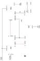
图5为根据本发明一个实施例的偏置与温测电路50。包括启动电路501、基准单元502(包括PTAT电流产生电路5021和基准电压产生电路5022)和反馈电路503。基准电压源电路50可以看作基准电压源电路40的一个具体实施例。FIG. 5 is a bias and
启动电路501包括:The
第一晶体管M1,具有第一端、第二端和控制端,其第一端耦接至地,其控制端耦接至启动电路的第一控制端;第一电阻R1,具有第一端和第二端,其第一端耦接至第一晶体管M1的第二端;第二晶体管M2,具有第一端、第二端和控制端,其第一端耦接至第一电阻R1的第二端,其控制端耦接至第二晶体管M2的第一端,其第二端耦接至启动电路的电源输入端;第三晶体管M3,具有第一端、第二端和控制端,其第一端耦接至启动电路的第二偏置端,其第二端耦接至启动电路电源的输入端VCC,其控制端耦接至第二晶体管M2的控制端;第五晶体管M5,具有第一端、第二端和控制端,其第二端耦接至启动电路的电源输入端,其控制端耦接至第二晶体管M2的控制端,其第一端耦接至启动电路的电源提供端。The first transistor M1 has a first terminal, a second terminal and a control terminal, its first terminal is coupled to the ground, and its control terminal is coupled to the first control terminal of the start-up circuit; the first resistor R1 has a first terminal and The second terminal, the first terminal of which is coupled to the second terminal of the first transistor M1; the second transistor M2 has a first terminal, a second terminal and a control terminal, and the first terminal of which is coupled to the first terminal of the first resistor R1 Two terminals, the control terminal of which is coupled to the first terminal of the second transistor M2, and the second terminal of which is coupled to the power input terminal of the startup circuit; the third transistor M3 has a first terminal, a second terminal and a control terminal, and its second terminal is coupled to the power input terminal of the startup circuit; The first terminal is coupled to the second bias terminal of the startup circuit, the second terminal thereof is coupled to the input terminal VCC of the power supply of the startup circuit, and the control terminal thereof is coupled to the control terminal of the second transistor M2; the fifth transistor M5 has The first terminal, the second terminal and the control terminal, the second terminal of which is coupled to the power input terminal of the startup circuit, the control terminal of which is coupled to the control terminal of the second transistor M2, and the first terminal of which is coupled to the power supply of the startup circuit Provide end.
基准单元502包括PTAT(proportional to absolute temperature,与绝对温度成正比)电流产生电路5021,用以产生PTAT电流;以及基准电压产生电路5022,镜像PTAT电流作为参考电流IREF,并产生基准电压VREF。The reference unit 502 includes a PTAT (proportional to absolute temperature, proportional to absolute temperature)
PTAT电流产生电路5021包括:The PTAT
第六晶体管M6,具有第一端、第二端和控制端,其第二端耦接至基准单元的电源端;第二电阻R2,具有第一端和第二端,其第二端耦接至第六晶体管M6的第一端,其第一端耦接至第六晶体管M6的控制端;第七晶体管M7,具有第一端、第二端和控制端,其第二端耦接至基准单元的电源端,其控制端耦接至第六晶体管M6的控制端;第三电阻R3,具有第一端和第二端,其第二端耦接至第七晶体管M7的第一端;第八晶体管M8,具有第一端、第二端和控制端,其第二端耦接至第二电阻R2的第一端,其控制端耦接至启动电路第二偏置端;第九晶体管M9,具有第一端、第二端和控制端,其第二端耦接至第三电阻R3的第一端,其控制端耦接至第八晶体管M8控制端和第三电阻R3的第二端;第四电阻R4,具有第一端和第二端,其第二端耦接至第八晶体管M8的第一端;第十晶体管Q10,具有第一端、第二端和控制端,其第一端和控制端耦接至地,其第二端耦接至第四电阻R4的第一端;第十一晶体管Q11,具有第一端、第二端和控制端,其第一端和控制端耦接至地,其第二端耦接至第九晶体管M9的第一端;第十四晶体管M14,具有第一端、第二端和控制端,其第一端耦接至地,其第二端耦接至基准单元的电源端,其控制端耦接至第九晶体管M9的第二端。The sixth transistor M6 has a first terminal, a second terminal and a control terminal, and its second terminal is coupled to the power supply terminal of the reference unit; the second resistor R2 has a first terminal and a second terminal, and its second terminal is coupled to To the first terminal of the sixth transistor M6, its first terminal is coupled to the control terminal of the sixth transistor M6; the seventh transistor M7 has a first terminal, a second terminal and a control terminal, and its second terminal is coupled to the reference The power terminal of the unit, the control terminal of which is coupled to the control terminal of the sixth transistor M6; the third resistor R3 has a first terminal and a second terminal, and the second terminal of which is coupled to the first terminal of the seventh transistor M7; The eight transistor M8 has a first terminal, a second terminal and a control terminal, the second terminal of which is coupled to the first terminal of the second resistor R2, and the control terminal of which is coupled to the second bias terminal of the starting circuit; the ninth transistor M9 , having a first terminal, a second terminal and a control terminal, the second terminal of which is coupled to the first terminal of the third resistor R3, and the control terminal of which is coupled to the control terminal of the eighth transistor M8 and the second terminal of the third resistor R3 The fourth resistor R4 has a first terminal and a second terminal, and its second terminal is coupled to the first terminal of the eighth transistor M8; the tenth transistor Q10 has a first terminal, a second terminal and a control terminal, and its second terminal is coupled to the first terminal of the eighth transistor M8; One terminal and the control terminal are coupled to ground, and the second terminal thereof is coupled to the first terminal of the fourth resistor R4; the eleventh transistor Q11 has a first terminal, a second terminal and a control terminal, and its first terminal is connected to the control terminal The terminal is coupled to the ground, and its second terminal is coupled to the first terminal of the ninth transistor M9; the fourteenth transistor M14 has a first terminal, a second terminal and a control terminal, its first terminal is coupled to the ground, and its The second terminal is coupled to the power supply terminal of the reference unit, and its control terminal is coupled to the second terminal of the ninth transistor M9.
PTAT电流产生电路2021采用了低电压结构,在不使用运算放大器情况下,即可产生PTAT电流。尤其是,电阻R2和电阻R3的引入,可以进一步降低基准单元202的最低工作电压,从而降低整个基准电压源200的最低工作电压。因此,PTAT电流产生电路2021也可以称为低电压基准源电路,用以产生PTAT电流或与基准电压产生电路2022组合以产生基准电压源。The PTAT current generating circuit 2021 adopts a low-voltage structure, and can generate PTAT current without using an operational amplifier. In particular, the introduction of the resistors R2 and R3 can further reduce the minimum operating voltage of the reference unit 202 , thereby reducing the minimum operating voltage of the entire reference voltage source 200 . Therefore, the PTAT current generating circuit 2021 can also be called a low-voltage reference source circuit for generating PTAT current or combined with the reference voltage generating circuit 2022 to generate a reference voltage source.
电压产生电路5022包括:The
第十五晶体管M15,具有第一端、第二端和控制端,其第二端耦接至基准单元的电源端,其第一端耦接至基准单元的电压提供端,其控制端耦接至第六晶体管M6的控制端;第四晶体管M4,具有第一端、第二端和控制端,其第二端耦接至基准单元的电源端,其第一端耦接至基准单元的温测端以提供温度检测信号VSES,其控制端耦接至第六晶体管M6的控制端。第五电阻R5,具有第一端和第二端,其第二端耦接至第十五晶体管M15的第一端,以及耦接至基准单元的电压提供端。第六电阻R6,具有第一端和第二端,其第二端耦接至第四晶体管M15的第一端,其第二端耦接至接地端。第十六晶体管Q16,具有第一端、第二端和控制端,其第一端和控制端耦接至地,其第二端耦接至第五电阻R5第一端。The fifteenth transistor M15 has a first terminal, a second terminal and a control terminal, its second terminal is coupled to the power terminal of the reference unit, its first terminal is coupled to the voltage supply terminal of the reference unit, and its control terminal is coupled to to the control terminal of the sixth transistor M6; the fourth transistor M4 has a first terminal, a second terminal and a control terminal, the second terminal of which is coupled to the power terminal of the reference unit, and the first terminal of which is coupled to the temperature of the reference unit The sense terminal is used to provide the temperature detection signal VSES, and the control terminal thereof is coupled to the control terminal of the sixth transistor M6. The fifth resistor R5 has a first terminal and a second terminal, the second terminal of which is coupled to the first terminal of the fifteenth transistor M15 and is coupled to the voltage supply terminal of the reference unit. The sixth resistor R6 has a first terminal and a second terminal, the second terminal of which is coupled to the first terminal of the fourth transistor M15, and the second terminal of which is coupled to the ground terminal. The sixteenth transistor Q16 has a first terminal, a second terminal and a control terminal, the first terminal and the control terminal are coupled to the ground, and the second terminal is coupled to the first terminal of the fifth resistor R5.
反馈电路503包括:
第十七晶体管M17,具有第一端、第二端和控制端,其第一端配置为反馈电路的控制端并耦接至启动电路第一偏置端,其第二端耦接至反馈电路的电源输入端;第十八晶体管M18,具有第一端、第二端和控制端,其第二端耦接至反馈电路的电源输入端,其控制端耦接至第十七晶体管M17的控制端;第十九晶体管M19,具有第一端、第二端和控制端,其第二端耦接至反馈电路的电源输入端,其控制端耦接至第十七晶体管M17的控制端;第二十晶体管M20,具有第一端、第二端和控制端,其第二端耦接至第十八晶体管M18的第一端,其第一端配置为反馈电路电源提供端以提供内部电源VINT;第二十一晶体管M21,具有第一端、第二端和控制端,其第二端耦接至第十九晶体管M19的第一端,其第二端耦接至第十九晶体管M19的控制端,其控制端耦接至第二十晶体管M20的控制端;第二十二晶体管M22,具有第一端、第二端和控制端,其第二端耦接至第二十晶体管M20的第一端,其控制端耦接至反馈电路偏置端;第二十三晶体管M23,具有第一端、第二端和控制端,其第一端耦接至地,其第二端耦接至第二十二晶体管M22的第一端,其控制端耦接至第二十三晶体管M23的第二端;第二十四晶体管M24,具有第一端、第二端和控制端,其第一端耦接至地,其第二端耦接至第二十一晶体管M21第一端,其控制端耦至第二十三晶体管M23的控制端;第二十五晶体管M25,具有第一端、第二端和控制端,其第一端耦接至接地端,其控制端耦接至第二十三晶体管M23的控制端;第二十六晶体管M26,具有第一端、第二端和控制端,其第一端耦接至第二十五晶体管M25的第二端,其控制端耦接至第二十六晶体管M26的第一端和第二十晶体管的控制端,其第二端耦接至反馈电路的电源输入端。The seventeenth transistor M17 has a first terminal, a second terminal and a control terminal, the first terminal of which is configured as the control terminal of the feedback circuit and is coupled to the first bias terminal of the start-up circuit, and the second terminal of which is coupled to the feedback circuit The power input end of the eighteenth transistor M18 has a first end, a second end and a control end, the second end of which is coupled to the power input end of the feedback circuit, and the control end is coupled to the control of the seventeenth transistor M17 terminal; the nineteenth transistor M19 has a first terminal, a second terminal and a control terminal, its second terminal is coupled to the power input terminal of the feedback circuit, and its control terminal is coupled to the control terminal of the seventeenth transistor M17; The twenty transistor M20 has a first terminal, a second terminal and a control terminal, the second terminal of which is coupled to the first terminal of the eighteenth transistor M18, and the first terminal of which is configured as a feedback circuit power supply terminal to provide the internal power supply VINT ; The twenty-first transistor M21 has a first terminal, a second terminal and a control terminal, its second terminal is coupled to the first terminal of the nineteenth transistor M19, and its second terminal is coupled to the nineteenth transistor M19 A control terminal, the control terminal of which is coupled to the control terminal of the twentieth transistor M20; the twenty-second transistor M22 has a first terminal, a second terminal and a control terminal, and the second terminal of which is coupled to the control terminal of the twentieth transistor M20 The first terminal, its control terminal is coupled to the bias terminal of the feedback circuit; the twenty-third transistor M23 has a first terminal, a second terminal and a control terminal, its first terminal is coupled to the ground, and its second terminal is coupled to To the first end of the twenty-second transistor M22, its control end is coupled to the second end of the twenty-third transistor M23; the twenty-fourth transistor M24 has a first end, a second end and a control end, and its first end One terminal is coupled to the ground, its second terminal is coupled to the first terminal of the twenty-first transistor M21, and its control terminal is coupled to the control terminal of the twenty-third transistor M23; the twenty-fifth transistor M25 has a first terminal , a second terminal and a control terminal, the first terminal of which is coupled to the ground terminal, and the control terminal of which is coupled to the control terminal of the twenty-third transistor M23; the twenty-sixth transistor M26 has a first terminal, a second terminal and The control terminal, its first terminal is coupled to the second terminal of the twenty-fifth transistor M25, its control terminal is coupled to the first terminal of the twenty-sixth transistor M26 and the control terminal of the twentieth transistor, its second terminal Coupled to the power input terminal of the feedback circuit.
电路工作原理如下:The working principle of the circuit is as follows:
启动电路包括M1、M2、M3、M5和R1,若EN高电压使能,M1导通,在M2上产生电流,M2、M3、M5工作,M3为基准单元提供偏置,M5为基准单元模块供电。基准单元模块包括M6、M7、M8、M9、Q10、Q11、R2、R3和R4。核心单元开始工作后,M6和M7所在的两条支路导通,产生PTAT电流,并通过M15镜像至电阻R5。电流IM15与电流IM8,IM9相等,M15、Q16、R5构成基准电压产生模块,Q10、Q11和Q16三者尺寸比为10:1:1(示例而非限制)。The start-up circuit includes M1, M2, M3, M5 and R1. If the EN high voltage is enabled, M1 is turned on to generate current on M2, M2, M3, and M5 work, M3 provides bias for the reference unit, and M5 is the reference unit module powered by. Reference cell modules include M6, M7, M8, M9, Q10, Q11, R2, R3, and R4. After the core unit starts to work, the two branches where M6 and M7 are located are turned on to generate PTAT current, which is mirrored to resistor R5 through M15. The current IM15 is equal to the currents IM8 and IM9, M15, Q16 and R5 form a reference voltage generating module, and the size ratio of Q10, Q11 and Q16 is 10:1:1 (example and not limitation).
基准电压值具体计算如下:The specific calculation of the reference voltage value is as follows:
VREF=VBE+KVT(2)VREF=VBE+KVT(2)
因此根据式(1)具体可得:Therefore, according to formula (1), we can get:
I1即为PTAT与绝对温度成正比的电流。I1 is the current proportional to the absolute temperature of PTAT.
因为M8、M9匹配,Because M8 and M9 match,
IM8=IM9=I1=IM15(4)IM8 = IM9 = I1 = IM15 (4)
根据式(2)可知:According to formula (2), it can be known that:
M6、M7导通后,M22产生电流,导致M23、M24和M25导通,M26、M21和M20(M18和M19)所在支路也导通,即M20所在支路开始为PTAT电流产生电路2021供电。M18和M19导通后,M17上开始流过电流,导致M2栅极电压升高,进而导致M2~M5关断,M5不再为基准单元202提供电源,基准单元2021主要靠M20所在支路提供电流。即,基准单元202启动前,启动电路501为基准单元202供电;基准单元502启动后,反馈电路503控制启动电路501停止为基准单元502供电(节省能耗同时避免电源VCC的噪声通过M5直接传递给基准单元502),反馈电路503为基准单元供电。基准单元502启动后,供电主要靠反馈电路503,由于反馈单元503具有反馈功能,基准电压VREF的电源抑制比得到提高。即,基准单元502提供了电源抑制功能(VINT到VREF)同时,反馈电路503还提供了电源抑制功能(VCC到VINT),从而使得基准电压源50获得更高的电源抑制比。After M6 and M7 are turned on, M22 generates a current, causing M23, M24 and M25 to be turned on, and the branches where M26, M21 and M20 (M18 and M19) are located are also turned on, that is, the branch where M20 is located starts to supply power to the PTAT current generating circuit 2021 . After M18 and M19 are turned on, current starts to flow through M17, which causes the gate voltage of M2 to rise, which in turn causes M2 to M5 to be turned off, and M5 no longer provides power for the reference unit 202, and the reference unit 2021 is mainly provided by the branch where M20 is located. current. That is, before the reference unit 202 starts, the start-up
图6示出根据本发明一个实施例的光波导器件60,其中6(a)为三维立体示意图,6(b)为切面图。与图2所示的光波导器件20相比,光波导器件60的衬底层进一步包括第一半导体层61(例如P沉底)和第二半导体层62(例如N外延),第二半导体层62即可用于集成多种半导体器件,例如电阻、电容、三极管、MOS管。Fig. 6 shows an
根据本发明一个实施例,所示波导层22和23的侧面(测试区域29非相邻一面)被第二半导体层,这样即可在波导层22和23侧面相邻的第二半导体层内集成加热电阻器(63和64)或其他器件。According to one embodiment of the present invention, the side surfaces of the shown waveguide layers 22 and 23 (the non-adjacent side of the test area 29) are covered with a second semiconductor layer, so that they can be integrated in the second semiconductor layer adjacent to the sides of the waveguide layers 22 and 23. heating resistors (63 and 64) or other devices.
根据本发明一个实施例,如6(C)所示沿XY面的切面图。波导层22和23下方集成了可以感应温度的感应晶体管(第十晶体管Q10、第十一晶体管Q11和第十六晶体管Q16)。由于这些器件紧邻波导层22和23,可以更好地检测波导层的温度。在其他实施例中,感应晶体管还可以集成于波导层两侧的第二半导体层内。According to an embodiment of the present invention, as shown in 6(C) is a sectional view along the XY plane. Sensing transistors (tenth transistor Q10 , eleventh transistor Q11 and sixteenth transistor Q16 ) capable of sensing temperature are integrated below the waveguide layers 22 and 23 . Due to the close proximity of these devices to the waveguide layers 22 and 23, the temperature of the waveguide layers can be better detected. In other embodiments, the sensing transistor can also be integrated in the second semiconductor layer on both sides of the waveguide layer.
图7示出根据本发明一个实施例的热光效应光波导检测装置70。与图1所示的热光效应光波导检测装置10相比,检测装置70不再基于第一放大器14的输出信号VA1进行检测,而是基于光波导器件的温度(即温度信号VSES)进行检测。检测装置10各种检测方法、步骤同样适用于检测装置70。FIG. 7 shows a thermo-optic effect optical
在本公开内容中所使用的量词“一个”、“一种”等不排除复数。文中的“第一”、“第二”等仅表示在实施例的描述中出现的先后顺序,以便于区分类似部件。“第一”、“第二”在权利要求书中的出现仅为了便于对权利要求的快速理解而不是为了对其进行限制。权利要求书中的任何附图标记都不应解释为对范围的限制。As used in this disclosure, the quantifiers "a", "an" etc. do not exclude a plural number. The "first", "second" and so on herein only indicate the order of appearance in the description of the embodiments, so as to distinguish similar components. The appearance of "first" and "second" in the claims is only to facilitate the quick understanding of the claims and not to limit them. Any reference signs in the claims should not be construed as limiting the scope.
Claims (9)
Translated fromChinesePriority Applications (1)
| Application Number | Priority Date | Filing Date | Title |
|---|---|---|---|
| CN201810105858.2ACN108303377B (en) | 2018-02-02 | 2018-02-02 | A thermo-optic effect optical waveguide detection device |
Applications Claiming Priority (1)
| Application Number | Priority Date | Filing Date | Title |
|---|---|---|---|
| CN201810105858.2ACN108303377B (en) | 2018-02-02 | 2018-02-02 | A thermo-optic effect optical waveguide detection device |
Publications (2)
| Publication Number | Publication Date |
|---|---|
| CN108303377A CN108303377A (en) | 2018-07-20 |
| CN108303377Btrue CN108303377B (en) | 2023-05-09 |
Family
ID=62864366
Family Applications (1)
| Application Number | Title | Priority Date | Filing Date |
|---|---|---|---|
| CN201810105858.2AActiveCN108303377B (en) | 2018-02-02 | 2018-02-02 | A thermo-optic effect optical waveguide detection device |
Country Status (1)
| Country | Link |
|---|---|
| CN (1) | CN108303377B (en) |
Citations (18)
| Publication number | Priority date | Publication date | Assignee | Title |
|---|---|---|---|---|
| US5073024A (en)* | 1988-11-04 | 1991-12-17 | Commissariat A L'energie Atomique | Integrated optical device for measuring the refractive index of a fluid |
| US5214724A (en)* | 1990-03-02 | 1993-05-25 | Fujitsu Limited | Optical waveguide device with suppressed dc drift |
| EP1139162A2 (en)* | 2000-03-21 | 2001-10-04 | Matsushita Electric Industrial Co., Ltd. | Optical waveguide elements, optical wavelength conversion elements, and process for producing optical waveguide elements |
| JP2002116164A (en)* | 2000-10-11 | 2002-04-19 | Univ Shizuoka | Thermo-optical constant measuring method for polymeric material and thermo-optical constant measuring method for polymeric thin film |
| JP2003322616A (en)* | 2002-04-30 | 2003-11-14 | National Institute Of Advanced Industrial & Technology | Refractive index measuring method and refractive index measuring device using the same |
| CN101021593A (en)* | 2007-03-16 | 2007-08-22 | 清华大学 | Integrated photon crystal double waveguide back coupling fluid refractive index sensor |
| CN101893562A (en)* | 2010-06-22 | 2010-11-24 | 浙江大学 | High-sensitivity integrated optical waveguide sensor device based on digital droplet sampling channel |
| CN102323239A (en)* | 2011-08-09 | 2012-01-18 | 哈尔滨工程大学 | Refractive index sensor based on asymmetric double-core optical fiber |
| WO2012026135A1 (en)* | 2010-08-27 | 2012-03-01 | 住友ベークライト株式会社 | Optical waveguide and electronic device |
| CN102565000A (en)* | 2012-01-10 | 2012-07-11 | 东南大学 | Multimode interference biological chemical sensor based on silicon slot waveguides |
| CN102608699A (en)* | 2012-01-12 | 2012-07-25 | 清华大学 | Short-range surface plasma waveguide and dielectric waveguide mixed coupling array type structure |
| CN103487405A (en)* | 2013-09-23 | 2014-01-01 | 电子科技大学 | Optical biochemical sensor based on spiral runway type interference structure |
| CN203479702U (en)* | 2013-05-16 | 2014-03-12 | 成都谱视科技有限公司 | SOI (silicon-on-insulator)-based slit optical waveguide grating FP (Fabry-Perot) cavity optical biochemical sensor chip |
| CN104316996A (en)* | 2014-11-03 | 2015-01-28 | 东南大学 | Waveguide Bragg grating refractive index sensor based on integrated polymers |
| CN104422669A (en)* | 2013-09-05 | 2015-03-18 | 周礼君 | Optical waveguide type particle plasma resonance sensing system |
| CN106899270A (en)* | 2017-04-13 | 2017-06-27 | 成都信息工程大学 | A kind of dynamic monitoring circuit |
| CN207923701U (en)* | 2018-02-02 | 2018-09-28 | 成都信息工程大学 | A kind of thermo-optic effect optical waveguide detection device |
| CN108613949A (en)* | 2018-07-30 | 2018-10-02 | 兰州理工大学 | The angle scanning index sensor of Medium Wave Guide is coated based on unsymmetrical metal |
Family Cites Families (3)
| Publication number | Priority date | Publication date | Assignee | Title |
|---|---|---|---|---|
| GB0707304D0 (en)* | 2007-04-16 | 2007-05-23 | Univ Southampton | Evanescent field optical waveguide devices |
| TW200915043A (en)* | 2007-09-29 | 2009-04-01 | Novatek Microelectronics Corp | Biasing circuit with fast response |
| US9442261B2 (en)* | 2014-07-09 | 2016-09-13 | Toshiba Medical Systems Corporation | Devices for coupling a light-emitting component and a photosensing component |
- 2018
- 2018-02-02CNCN201810105858.2Apatent/CN108303377B/enactiveActive
Patent Citations (18)
| Publication number | Priority date | Publication date | Assignee | Title |
|---|---|---|---|---|
| US5073024A (en)* | 1988-11-04 | 1991-12-17 | Commissariat A L'energie Atomique | Integrated optical device for measuring the refractive index of a fluid |
| US5214724A (en)* | 1990-03-02 | 1993-05-25 | Fujitsu Limited | Optical waveguide device with suppressed dc drift |
| EP1139162A2 (en)* | 2000-03-21 | 2001-10-04 | Matsushita Electric Industrial Co., Ltd. | Optical waveguide elements, optical wavelength conversion elements, and process for producing optical waveguide elements |
| JP2002116164A (en)* | 2000-10-11 | 2002-04-19 | Univ Shizuoka | Thermo-optical constant measuring method for polymeric material and thermo-optical constant measuring method for polymeric thin film |
| JP2003322616A (en)* | 2002-04-30 | 2003-11-14 | National Institute Of Advanced Industrial & Technology | Refractive index measuring method and refractive index measuring device using the same |
| CN101021593A (en)* | 2007-03-16 | 2007-08-22 | 清华大学 | Integrated photon crystal double waveguide back coupling fluid refractive index sensor |
| CN101893562A (en)* | 2010-06-22 | 2010-11-24 | 浙江大学 | High-sensitivity integrated optical waveguide sensor device based on digital droplet sampling channel |
| WO2012026135A1 (en)* | 2010-08-27 | 2012-03-01 | 住友ベークライト株式会社 | Optical waveguide and electronic device |
| CN102323239A (en)* | 2011-08-09 | 2012-01-18 | 哈尔滨工程大学 | Refractive index sensor based on asymmetric double-core optical fiber |
| CN102565000A (en)* | 2012-01-10 | 2012-07-11 | 东南大学 | Multimode interference biological chemical sensor based on silicon slot waveguides |
| CN102608699A (en)* | 2012-01-12 | 2012-07-25 | 清华大学 | Short-range surface plasma waveguide and dielectric waveguide mixed coupling array type structure |
| CN203479702U (en)* | 2013-05-16 | 2014-03-12 | 成都谱视科技有限公司 | SOI (silicon-on-insulator)-based slit optical waveguide grating FP (Fabry-Perot) cavity optical biochemical sensor chip |
| CN104422669A (en)* | 2013-09-05 | 2015-03-18 | 周礼君 | Optical waveguide type particle plasma resonance sensing system |
| CN103487405A (en)* | 2013-09-23 | 2014-01-01 | 电子科技大学 | Optical biochemical sensor based on spiral runway type interference structure |
| CN104316996A (en)* | 2014-11-03 | 2015-01-28 | 东南大学 | Waveguide Bragg grating refractive index sensor based on integrated polymers |
| CN106899270A (en)* | 2017-04-13 | 2017-06-27 | 成都信息工程大学 | A kind of dynamic monitoring circuit |
| CN207923701U (en)* | 2018-02-02 | 2018-09-28 | 成都信息工程大学 | A kind of thermo-optic effect optical waveguide detection device |
| CN108613949A (en)* | 2018-07-30 | 2018-10-02 | 兰州理工大学 | The angle scanning index sensor of Medium Wave Guide is coated based on unsymmetrical metal |
Non-Patent Citations (4)
| Title |
|---|
| Highly sensitive sensors of fluid detection based on magneto optical tamm state;Nengxi Li;《Sensors and actuators B:Chemical》;第第265卷卷;第644-651页* |
| Surface plasmon resonance refractive index sensor based on ultraviolet bleached polymer waveguide;Lanting Ji;《Sensors and Actuators B: Chemical》;第第244卷卷;第373-379页* |
| 二氧化硅光波导干涉微结构器件传感研究;鲍海泓;《中国优秀硕士学位论文全文数据库信息科技辑》;全文* |
| 基于磁光波导的液体折射率传感特性研究;张艳芬;《激光技术》;第第41卷卷(第第4期期);第554-557页* |
Also Published As
| Publication number | Publication date |
|---|---|
| CN108303377A (en) | 2018-07-20 |
Similar Documents
| Publication | Publication Date | Title |
|---|---|---|
| Islam et al. | A digital hygrometer for trace moisture measurement | |
| O’Toole et al. | Photometric detection in flow analysis systems using integrated PEDDs | |
| CN106679842B (en) | A kind of temp measuring method and temperature measurement circuit using reference voltage compensation technology | |
| CN106989847A (en) | Error correcting method in system of Pt-resistance | |
| CN108801981A (en) | Trace quantity liquid refractivity measuring device based on self-mixed interference and measurement method | |
| CN207923701U (en) | A kind of thermo-optic effect optical waveguide detection device | |
| CN108051406B (en) | An electro-optic effect optical waveguide detection device | |
| CN207894823U (en) | A kind of electrooptic effect optical waveguide detection device | |
| Nieh et al. | An Arduino-based experimental setup for teaching light color mixing, light intensity detection, and ambient temperature sensing | |
| CN108303377B (en) | A thermo-optic effect optical waveguide detection device | |
| CN108489632B (en) | A Method of Improving the Temperature Measurement Accuracy of Fluorescence Intensity Ratio Technique | |
| Limodehi et al. | Multi-channel fiber optic dew and humidity sensor | |
| Chen et al. | A low cost surface plasmon resonance biosensor using a laser line generator | |
| CN105044028B (en) | For detecting the universal on-line industry refractometer and detection method of solution concentration | |
| CN208721577U (en) | A device for detecting sugar content in liquid by light intensity | |
| Smith et al. | An integrated portable hand-held analyser for real-time isothermal nucleic acid amplification | |
| Kamarudin et al. | Flexible and autonomous integrated system for characterizing metal oxide gas sensor response in dynamic environment | |
| Umar et al. | Precise method for accuracy and sensitivity improvement of a current mirror for very low current measurement on a dissolved oxygen biosensor | |
| CN111076846B (en) | Test method and test system for body temperature probe | |
| Karandikar et al. | Low power, low noise, compact amperometric circuit for three-terminal glucose biosensor | |
| Freisa et al. | Microcalorimeter fabrication and new measurement methodology for thermal sensing in microfluidics | |
| Wang et al. | Refractive index sensing based on Mach–Zehnder interferometer with a hybrid silica/polymer waveguide | |
| Okan et al. | A microfluidic based differential plasmon resonance sensor | |
| Postolache et al. | Dew point and relative-humidity smart measuring system | |
| Agrawal et al. | Evaluation of developed colorimeter for glucose estimation in water |
Legal Events
| Date | Code | Title | Description |
|---|---|---|---|
| PB01 | Publication | ||
| PB01 | Publication | ||
| SE01 | Entry into force of request for substantive examination | ||
| SE01 | Entry into force of request for substantive examination | ||
| GR01 | Patent grant | ||
| GR01 | Patent grant |