CN108292677B - Folded form terminal with internal field board - Google Patents
Folded form terminal with internal field boardDownload PDFInfo
- Publication number
- CN108292677B CN108292677BCN201680057871.4ACN201680057871ACN108292677BCN 108292677 BCN108292677 BCN 108292677BCN 201680057871 ACN201680057871 ACN 201680057871ACN 108292677 BCN108292677 BCN 108292677B
- Authority
- CN
- China
- Prior art keywords
- region
- type semiconductor
- semiconductor
- field plate
- trench
- Prior art date
- Legal status (The legal status is an assumption and is not a legal conclusion. Google has not performed a legal analysis and makes no representation as to the accuracy of the status listed.)
- Expired - Fee Related
Links
- 239000004065semiconductorSubstances0.000claimsdescription126
- 238000002513implantationMethods0.000claimsdescription40
- 229910021420polycrystalline siliconInorganic materials0.000claimsdescription38
- 229920005591polysiliconPolymers0.000claimsdescription38
- 229910052751metalInorganic materials0.000claimsdescription15
- 239000002184metalSubstances0.000claimsdescription15
- 239000000758substrateSubstances0.000claimsdescription13
- 230000003247decreasing effectEffects0.000claimsdescription3
- 239000012535impuritySubstances0.000claimsdescription2
- 239000002019doping agentSubstances0.000claims2
- 230000015556catabolic processEffects0.000abstractdescription14
- 230000005684electric fieldEffects0.000abstractdescription14
- 239000000463materialSubstances0.000description20
- 238000005468ion implantationMethods0.000description9
- 238000004519manufacturing processMethods0.000description9
- XUIMIQQOPSSXEZ-UHFFFAOYSA-NSiliconChemical compound[Si]XUIMIQQOPSSXEZ-UHFFFAOYSA-N0.000description6
- 238000000034methodMethods0.000description6
- 229910052710siliconInorganic materials0.000description5
- 239000010703siliconSubstances0.000description5
- 235000012431wafersNutrition0.000description5
- VYPSYNLAJGMNEJ-UHFFFAOYSA-NSilicium dioxideChemical compoundO=[Si]=OVYPSYNLAJGMNEJ-UHFFFAOYSA-N0.000description4
- 238000005530etchingMethods0.000description4
- 230000000694effectsEffects0.000description3
- 238000000206photolithographyMethods0.000description3
- QVGXLLKOCUKJST-UHFFFAOYSA-Natomic oxygenChemical compound[O]QVGXLLKOCUKJST-UHFFFAOYSA-N0.000description2
- 238000005452bendingMethods0.000description2
- 238000010586diagramMethods0.000description2
- 229910052760oxygenInorganic materials0.000description2
- 239000001301oxygenSubstances0.000description2
- 235000012239silicon dioxideNutrition0.000description2
- 239000000377silicon dioxideSubstances0.000description2
- JBRZTFJDHDCESZ-UHFFFAOYSA-NAsGaChemical compound[As]#[Ga]JBRZTFJDHDCESZ-UHFFFAOYSA-N0.000description1
- ZOXJGFHDIHLPTG-UHFFFAOYSA-NBoronChemical compound[B]ZOXJGFHDIHLPTG-UHFFFAOYSA-N0.000description1
- 229910001218Gallium arsenideInorganic materials0.000description1
- GPXJNWSHGFTCBW-UHFFFAOYSA-NIndium phosphideChemical compound[In]#PGPXJNWSHGFTCBW-UHFFFAOYSA-N0.000description1
- 229910000577Silicon-germaniumInorganic materials0.000description1
- LEVVHYCKPQWKOP-UHFFFAOYSA-N[Si].[Ge]Chemical compound[Si].[Ge]LEVVHYCKPQWKOP-UHFFFAOYSA-N0.000description1
- 230000004913activationEffects0.000description1
- 230000009286beneficial effectEffects0.000description1
- 230000000903blocking effectEffects0.000description1
- 229910052796boronInorganic materials0.000description1
- 239000013078crystalSubstances0.000description1
- 238000000151depositionMethods0.000description1
- 238000009792diffusion processMethods0.000description1
- 230000007774longtermEffects0.000description1
- 230000003647oxidationEffects0.000description1
- 238000007254oxidation reactionMethods0.000description1
- 238000004806packaging method and processMethods0.000description1
- HBMJWWWQQXIZIP-UHFFFAOYSA-Nsilicon carbideChemical compound[Si+]#[C-]HBMJWWWQQXIZIP-UHFFFAOYSA-N0.000description1
- 229910010271silicon carbideInorganic materials0.000description1
- 239000002699waste materialSubstances0.000description1
Images


Classifications
- H—ELECTRICITY
- H10—SEMICONDUCTOR DEVICES; ELECTRIC SOLID-STATE DEVICES NOT OTHERWISE PROVIDED FOR
- H10D—INORGANIC ELECTRIC SEMICONDUCTOR DEVICES
- H10D62/00—Semiconductor bodies, or regions thereof, of devices having potential barriers
- H10D62/10—Shapes, relative sizes or dispositions of the regions of the semiconductor bodies; Shapes of the semiconductor bodies
- H10D62/102—Constructional design considerations for preventing surface leakage or controlling electric field concentration
- H10D62/103—Constructional design considerations for preventing surface leakage or controlling electric field concentration for increasing or controlling the breakdown voltage of reverse-biased devices
- H10D62/105—Constructional design considerations for preventing surface leakage or controlling electric field concentration for increasing or controlling the breakdown voltage of reverse-biased devices by having particular doping profiles, shapes or arrangements of PN junctions; by having supplementary regions, e.g. junction termination extension [JTE]
- H—ELECTRICITY
- H10—SEMICONDUCTOR DEVICES; ELECTRIC SOLID-STATE DEVICES NOT OTHERWISE PROVIDED FOR
- H10D—INORGANIC ELECTRIC SEMICONDUCTOR DEVICES
- H10D30/00—Field-effect transistors [FET]
- H10D30/60—Insulated-gate field-effect transistors [IGFET]
- H—ELECTRICITY
- H10—SEMICONDUCTOR DEVICES; ELECTRIC SOLID-STATE DEVICES NOT OTHERWISE PROVIDED FOR
- H10D—INORGANIC ELECTRIC SEMICONDUCTOR DEVICES
- H10D30/00—Field-effect transistors [FET]
- H10D30/60—Insulated-gate field-effect transistors [IGFET]
- H10D30/64—Double-diffused metal-oxide semiconductor [DMOS] FETs
- H10D30/65—Lateral DMOS [LDMOS] FETs
- H10D30/655—Lateral DMOS [LDMOS] FETs having edge termination structures
- H—ELECTRICITY
- H10—SEMICONDUCTOR DEVICES; ELECTRIC SOLID-STATE DEVICES NOT OTHERWISE PROVIDED FOR
- H10D—INORGANIC ELECTRIC SEMICONDUCTOR DEVICES
- H10D30/00—Field-effect transistors [FET]
- H10D30/60—Insulated-gate field-effect transistors [IGFET]
- H10D30/64—Double-diffused metal-oxide semiconductor [DMOS] FETs
- H10D30/66—Vertical DMOS [VDMOS] FETs
- H10D30/665—Vertical DMOS [VDMOS] FETs having edge termination structures
- H—ELECTRICITY
- H10—SEMICONDUCTOR DEVICES; ELECTRIC SOLID-STATE DEVICES NOT OTHERWISE PROVIDED FOR
- H10D—INORGANIC ELECTRIC SEMICONDUCTOR DEVICES
- H10D30/00—Field-effect transistors [FET]
- H10D30/60—Insulated-gate field-effect transistors [IGFET]
- H10D30/64—Double-diffused metal-oxide semiconductor [DMOS] FETs
- H10D30/66—Vertical DMOS [VDMOS] FETs
- H10D30/668—Vertical DMOS [VDMOS] FETs having trench gate electrodes, e.g. UMOS transistors
- H—ELECTRICITY
- H10—SEMICONDUCTOR DEVICES; ELECTRIC SOLID-STATE DEVICES NOT OTHERWISE PROVIDED FOR
- H10D—INORGANIC ELECTRIC SEMICONDUCTOR DEVICES
- H10D62/00—Semiconductor bodies, or regions thereof, of devices having potential barriers
- H10D62/10—Shapes, relative sizes or dispositions of the regions of the semiconductor bodies; Shapes of the semiconductor bodies
- H10D62/102—Constructional design considerations for preventing surface leakage or controlling electric field concentration
- H10D62/112—Constructional design considerations for preventing surface leakage or controlling electric field concentration for preventing surface leakage due to surface inversion layers, e.g. by using channel stoppers
- H—ELECTRICITY
- H10—SEMICONDUCTOR DEVICES; ELECTRIC SOLID-STATE DEVICES NOT OTHERWISE PROVIDED FOR
- H10D—INORGANIC ELECTRIC SEMICONDUCTOR DEVICES
- H10D64/00—Electrodes of devices having potential barriers
- H10D64/111—Field plates
- H10D64/117—Recessed field plates, e.g. trench field plates or buried field plates
Landscapes
- Electrodes Of Semiconductors (AREA)
- Insulated Gate Type Field-Effect Transistor (AREA)
Abstract
Translated fromChinese
Description
Translated fromChinese技术领域technical field
本发明属于半导体技术领域,涉及一种具有体内场板的折叠型终端结构。The invention belongs to the technical field of semiconductors, and relates to a foldable terminal structure with an internal field plate.
背景技术Background technique
功率器件阻断高压的能力主要取决于器件结构中特定PN结的反偏击穿电压。所有半导体器件的尺寸都是有限的,将晶圆切割成芯片进行封装制成器件。切割过程中会对硅片的晶格造成很大的损伤。对于功率器件而言,如果切割穿过了承受高压的器件结构区,晶格损伤会引起很大的漏电流,这会降低器件的击穿电压和长期稳定性。在功率器件中,受PN结弯曲或PN结终止处表面非理想因素的影响,反偏PN结击穿电压又受限于发生在表面附近或结弯曲处局部区域相对于体内平行平面结提前出现的击穿现象。结终端就是为了减小局部电场、提高表面击穿电压及可靠性、使器件实际击穿电压更接近平行平面结理想值而专门设计的特殊结构。在纵向导电器件中它通常分布在器件有源区的周边,是有源区内用于承受外高压的PN结的附属结构。The ability of a power device to block high voltages mainly depends on the reverse-biased breakdown voltage of a particular PN junction in the device structure. All semiconductor devices are limited in size, and wafers are diced into chips for packaging to make devices. The dicing process will cause great damage to the crystal lattice of the silicon wafer. For power devices, lattice damage can cause large leakage currents if the cut passes through regions of the device structure that are subjected to high voltages, which can reduce the breakdown voltage and long-term stability of the device. In power devices, the reverse-biased PN junction breakdown voltage is limited to occur near the surface or the local area at the junction bending due to the influence of the PN junction bending or surface non-ideal factors at the termination of the PN junction relative to the parallel plane junction in the body. breakdown phenomenon. The junction terminal is a special structure specially designed to reduce the local electric field, improve the surface breakdown voltage and reliability, and make the actual breakdown voltage of the device closer to the ideal value of the parallel plane junction. In vertical conductive devices, it is usually distributed around the active region of the device, and is a subsidiary structure of the PN junction used to withstand external high voltages in the active region.
目前,采用平面工艺制作的功率半导体器件,其结终端结构主要是在主结边缘处(常是弯曲的)设置一些延伸结构,这些延伸结构实际上起到将主结耗尽区向外展宽的作用,从而降低其内的电场强度最终提高击穿电压,如场板(FP)、场限环(FLR)、结终端扩展(JTE)、横向变掺杂(VLD)、阻性场板(如掺氧多晶硅(SIPOS))、RESURF等。要实现高的耐压,延伸结构必须足够长,以保证耗尽区充分扩散。因此,在高压器件中,现有的延伸型终端结构所占用面积都太大,造成器件成本的上升。At present, the junction termination structure of a power semiconductor device fabricated by a planar process is mainly to set some extension structures at the edge of the main junction (often curved), and these extension structures actually serve to widen the depletion region of the main junction outwards. effect, thereby reducing the electric field strength in it and finally increasing the breakdown voltage, such as field plate (FP), field limiting ring (FLR), junction termination extension (JTE), laterally variable doping (VLD), resistive field plate (such as Oxygen-doped polysilicon (SIPOS)), RESURF, etc. To achieve high withstand voltage, the extension structure must be long enough to ensure adequate diffusion of the depletion region. Therefore, in a high-voltage device, the area occupied by the existing extended terminal structure is too large, resulting in an increase in the cost of the device.
发明内容SUMMARY OF THE INVENTION
本发明所要解决的,就是针对上述问题,提出一种在相同耐压的情况下获得比常规结构更小的面积的具有体内场板的终端结构。The purpose of the present invention is to solve the above problems, and to propose a terminal structure with an internal field plate which can obtain a smaller area than the conventional structure under the same withstand voltage.
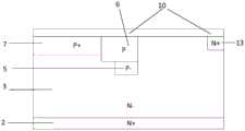
本发明的技术方案是:一种具有体内场板的折叠型终端结构,包括第一导电类型半导体重掺杂衬底2、位于第一导电类型半导体重掺杂衬底2上表面的第一导电类型半导体轻掺杂漂移区3和位于第一导电类型半导体重掺杂衬底2下表面的金属漏电极1;其特征在于,所述第一导电类型半导体轻掺杂漂移区3中具有沟槽4,所述沟槽4位于第一导电类型半导体轻掺杂漂移区3中部,并沿第一导电类型半导体轻掺杂漂移区3上表面垂直向下延伸入第一导电类型半导体轻掺杂漂移区3中,所述沟槽4中填充有绝缘介质;所述第一导电类型半导体轻掺杂漂移区3上表面具有场氧化层10;所述沟槽4靠近器件有源区的一侧具有第一半导体注入区6,所述第一半导体注入区6分别与有源区的第二导电类型半导体主结7和沟槽4接触,第一半导体注入区6的上表面与场氧化层10接触;所述第一半导体注入区6的下表面连接有第二半导体注入区5,所述第二半导体注入区5的侧面与沟槽4接触;所述第一半导体注入区6与第二半导体注入区5为第二导电类型半导体,且第一半导体注入区6的掺杂浓度大于第二半导体注入区5;所述第一导电类型半导体轻掺杂漂移区3上层远离器件有源区的一端具有第一导电类型半导体的重掺杂区13,所述第一导电类型半导体的重掺杂区13的上表面与场氧化层10接触;所述场氧化层10的上表面具有多晶硅层9;所述沟槽4中具有多晶硅场板8,所述多晶硅场板8的上表面与多晶硅层9接触。The technical scheme of the present invention is: a folded terminal structure with an internal field plate, comprising a first conductive type semiconductor heavily doped
进一步的,多晶硅场板8在器件的剖面图中呈倒梯形,且多晶硅场板8下底边的深度大于第二半导体注入区5的结深,多晶硅场板8的侧边与水平线的夹角θ的取值在60°到70°之间。Further, the
进一步的,所述沟槽4的正下方具有第二导电类型半导体埋层14。Further, there is a second conductive type semiconductor buried
进一步的,所述沟槽4的下表面延伸至第一导电类型半导体重掺杂衬底2中。Further, the lower surface of the
进一步的,所述第二半导体注入区5下方沿沟槽4的侧壁还设置有多个掺杂浓度依次降低的半导体掺杂区。Further, a plurality of semiconductor doping regions with the doping concentration decreasing in sequence are also provided below the second
进一步的,所述器件有源区中,在第一导电类型半导体轻掺杂漂移区3上层具有与第一半导体注入区6接触的第二导电类型半导体的主结7,所述第二导电类型半导体的主结7上表面远离终端区的一端具有源极金属11,所述源极金属11与场氧化层10接触。Further, in the active region of the device, there is a
进一步的,所述第二导电类型半导体的主结7通过接触孔与多晶硅层9连接。Further, the
进一步的,所述源极金属11沿场氧化层10上表面延伸至与多晶硅层9连接,将源极的电位接到多晶硅场板8上。Further, the
进一步的,所述沟槽4的正下方具有第二导电类型半导体埋层14。Further, there is a second conductive type semiconductor buried
本发明的有益效果为,相对于传统结构,本发明将场板结构和结终端扩展区向器件内部折叠,可以充分利用体内漂移区厚度,从而缩小终端的横向面积,缓解了PN结终止端的电场集中,击穿点的位置从原来的PN结的终止端转移到了体内,终端的耐压能达到平行平面结的击穿电压;因此,本发明提出的具有体内场板的折叠式终端结构的终端效率要远高于常规的结终端扩展结构。The beneficial effect of the present invention is that, compared with the traditional structure, the present invention folds the field plate structure and the extension region of the junction terminal to the inside of the device, which can make full use of the thickness of the drift region in the body, thereby reducing the lateral area of the terminal and alleviating the electric field at the termination end of the PN junction. Concentration, the position of the breakdown point is transferred from the termination end of the original PN junction to the body, and the withstand voltage of the termination can reach the breakdown voltage of the parallel plane junction; Efficiency is much higher than conventional junction termination extension structures.
附图说明Description of drawings
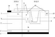
图1为实施例1的结构示意图;Fig. 1 is the structural representation of
图2为常规平面型结终端扩展结构在漏端加高电压时,耗尽线示意图;FIG. 2 is a schematic diagram of a depletion line when a high voltage is applied to the drain terminal of a conventional planar junction terminal extension structure;
图3为实施例1制造流程中高能离子注入后形成第二导电类型半导体材料轻掺杂区5的剖视图;3 is a cross-sectional view of forming a lightly doped
图4为实施例1制造流程中离子注入后形成第二导电类型半导体材料轻掺杂区6的剖视图;FIG. 4 is a cross-sectional view of forming a lightly doped
图5为实施例1制造流程中在有源区进行离子注入形成第二导电类型半导体材料掺杂区7的剖视图;5 is a cross-sectional view of ion implantation in the active region to form a
图6为实施例1制造流程中终端区经过离子注入后形成第一导电类型半导体材料重掺杂区13的剖视图;6 is a cross-sectional view of the heavily doped
图7为实施例1制造流程中在器件表面生长一层场氧化层后的剖视图;7 is a cross-sectional view after a field oxide layer is grown on the surface of the device in the manufacturing process of Example 1;
图8为实施例1制造流程中在终端区刻蚀出沟槽,并在槽中填充绝缘介质后的剖视图;8 is a cross-sectional view after etching a trench in the termination region and filling the trench with an insulating medium in the manufacturing process of
图9为实施例1制造流程中在终端区刻蚀出倒梯形的槽,同时将有源区第二导电类型半导体材料掺杂区7上表面的氧化层刻蚀掉,并在槽中及器件表面淀积多晶硅后的剖视图;FIG. 9 shows an inverted trapezoidal groove etched in the terminal region in the manufacturing process of the
图10是实施例2的结构示意图;Fig. 10 is the structural representation of
图11是实施例3的结构示意图;Fig. 11 is the structural representation of
图12是实施例4的结构示意图;Fig. 12 is the structural representation of
图13是实施例5的结构示意图;Fig. 13 is the structural representation of
图14是实施例6的结构示意图;Fig. 14 is the structural representation of
图15是实施例7的结构示意图。FIG. 15 is a schematic structural diagram of
具体实施方式Detailed ways
下面结合附图和实施例,详细描述本发明的技术方案:Below in conjunction with the accompanying drawings and embodiments, the technical solutions of the present invention are described in detail:
实施例1Example 1
如图1所示,本例的具有体内场板的终端结构,包括第一导电类型半导体重掺杂衬底2、位于第一导电类型半导体重掺杂衬底2上表面的第一导电类型半导体轻掺杂漂移区3和位于第一导电类型半导体重掺杂衬底2下表面的金属漏电极1;其特征在于,所述第一导电类型半导体轻掺杂漂移区3中具有沟槽4,所述沟槽4位于第一导电类型半导体轻掺杂漂移区3中部,并沿第一导电类型半导体轻掺杂漂移区3上表面垂直向下延伸入第一导电类型半导体轻掺杂漂移区3中,所述沟槽4中填充有绝缘介质;所述第一导电类型半导体轻掺杂漂移区3上表面具有场氧化层10;所述沟槽4靠近器件有源区的一侧具有第一半导体注入区6,所述第一半导体注入区6分别与有源区的第二导电类型半导体器件主结7和沟槽4接触,第一半导体注入区6的上表面与场氧化层10接触;所述第一半导体注入区6的下表面连接有第二半导体注入区5,所述第二半导体注入区5的侧面与沟槽4接触;所述第一半导体注入区6与第二半导体注入区5为第二导电类型半导体,且第一半导体注入区6的掺杂浓度大于第二半导体注入区5;所述第一导电类型半导体轻掺杂漂移区3上层远离器件有源区的一端具有第一导电类型半导体的重掺杂区13,所述第一导电类型半导体的重掺杂区13的上表面与场氧化层10接触;所述场氧化层10的上表面具有多晶硅层9;所述沟槽4中具有多晶硅场板8,所述多晶硅场板8的上表面与多晶硅层9接触;多晶硅场板8在器件的剖面图中呈倒梯形,且多晶硅场板8下底边的结深大于第二半导体注入区5的结深,多晶硅场板8的侧边与水平线的夹角θ的取值在60°到70°之间。As shown in FIG. 1 , the terminal structure with the internal field plate in this example includes a first conductive type semiconductor heavily doped
以第一导电类型半导体为P型半导体为例,说明本例的工作原理和制造方法。Taking the first conductivity type semiconductor as a P-type semiconductor as an example, the working principle and the manufacturing method of this example will be described.
图2为常规平面型结终端扩展结构,当功率器件处于反向阻断状态时,在漏极金属1上接正偏压,源极金属8上接零电位,电场由第一导电类型半导体轻掺杂区3指向第二导电类型半导体材料的主结5、第二导电类型半导体材料轻掺杂区6以及第二导电类型半导体材料更轻掺杂区7。该结构能极大的改善主结5边缘处的电场集中,提高击穿电压。但是,由于第二导电类型半导体材料轻掺杂区6以及第二导电类型半导体材料更轻掺杂区7均在半导体表面展开,需要较大的面积。Figure 2 shows a conventional planar junction terminal extension structure. When the power device is in the reverse blocking state, a positive bias voltage is connected to the
本例相比与传统结构,在第二导电类型半导体材料的主结5的侧面挖一沟槽,在沟槽侧面形成掺杂浓度依次降低的第二导电类型注入区6和第二导电类型注入区5,将结终端扩展区从表面引向体内,利用第一导电类型半导体轻掺杂漂移区3的厚度来扩展终端电场,有效节省了表面积。第二导电类型注入区6和第二导电类型注入区5构成结终端扩展(JTE)区。必须精确控制JTE区电荷来最大化击穿电压,如果电荷量过小,对电场的影响有限,如果JTE区的电荷量过大,耗尽区边缘曲率半径过小,击穿电压也会降低。因此,JTE区的电荷应正好被反向偏压完全耗尽。Compared with the conventional structure in this example, a trench is dug on the side of the
同时,本例在沟槽区4的内部挖槽并填充多晶硅作为场板,场板的下边缘超过第二导电类型半导体材料更轻掺杂区5的下表面,场板与第二导电类型半导体材料的主结7通过多晶硅相连。因此,场板与主结7等电位,可以进一步将耗尽区边界向第一导电类型半导体轻掺杂区3的体内延伸。场板的另一个优点是可以屏蔽氧化层中电荷对终端电场的影响。沟槽刻蚀和场氧生长工艺中极易带来附加电荷,由于有场板的存在,本发明提出的终端结构的可靠性也得到了提高。At the same time, in this example, a trench is dug inside the
常规的场板结构中电场在场板的末端会出现一个较大的值,这是由于在场氧厚度一定的情况下场板末端的氧化层两端的电势差是最大的。为了减小该处的电场,本例中在刻蚀多晶硅场板8的时候将槽刻成倒梯形,这就使得在纵向上二氧化硅层的厚度从第一导电类型半导体轻掺杂漂移区3的表面向体内是逐渐增加的,保证了不会因为场板的末端电场过大而导致器件提前击穿。多晶硅场板8的侧壁与水平方向的夹角角度θ是一个关键参数。一方面,过大的角度使得二氧化硅层厚度增加得不明显,即减缓场板末端电场的作用不明显。另一方面,过小的角度会使终端的面积过大,容易造成不必要的浪费。综上,θ的取值在60°到70°之间较为合适。In the conventional field plate structure, the electric field will have a larger value at the end of the field plate, because the potential difference between the two ends of the oxide layer at the end of the field plate is the largest when the thickness of the field oxygen is constant. In order to reduce the electric field there, in this example, when the
本例的工艺制造流程为:The manufacturing process of this example is:
(1)在N+衬底上外延生长N—掺杂浓度的漂移区,然后在硅片表面生长一层薄的预氧化层;(1) Epitaxially growing the drift region of N- doping concentration on the N+ substrate, and then growing a thin pre-oxidation layer on the surface of the silicon wafer;
(2)通过高能离子注入在终端区内部形成第二导电类型半导体轻掺杂区5,如图3所示;(2) forming a second conductive type semiconductor lightly doped
(3)在终端区进行光刻,并进行离子注入,在终端区形成第二导电类型半导体材料轻掺杂区6,之后通过高温推进过程使得轻掺杂区6与轻掺杂区5刚好接触。紧接着进行高温激活,使得杂质原子与晶格中的硅原子键合,如图4所示;(3) Perform photolithography in the terminal area and perform ion implantation to form a lightly doped
(4)光刻有源区,并进行离子注入,形成第二导电类型半导体材料掺杂区7。并通过热推进过程使得p型半导体材料掺杂区7达到一定的结深,并进行高温激活,如图5所示;(4) Photolithography of the active region and ion implantation to form the second conductive type semiconductor material doped
(5)在终端区进行光刻,并进行离子注入,形成第一导电类型半导体材料重掺杂区8,如图6所示;(5) photolithography is performed in the terminal region, and ion implantation is performed to form a heavily doped
(6)在硅片表面生长场氧化层10,如图7所示;(6) growing the
(7)在终端区刻蚀出一个的矩形槽4,并在槽中填充绝缘介质,如图8所示;(7) A
(8)在终端区刻蚀出倒梯形的槽,同时将有源区第二导电类型半导体材料掺杂区7表面的氧化层刻蚀掉,并在槽中及器件表面淀积多晶硅,如图9所示;(8) Etch an inverted trapezoidal groove in the terminal area, at the same time etch away the oxide layer on the surface of the second conductive type semiconductor material doped
(9)刻蚀形成接触孔,进行低能量高剂量的硼离子注入,在接触孔内形成P+接触区;淀积金属,并反刻金属,形成源电极。对硅片背面减薄,金属化形成漏极金属,如图1所示。(9) Etching to form a contact hole, performing low-energy and high-dose boron ion implantation to form a P+ contact region in the contact hole; depositing metal, and reverse-etching the metal to form a source electrode. The backside of the silicon wafer is thinned and metallized to form the drain metal, as shown in Figure 1.
实施例2Example 2
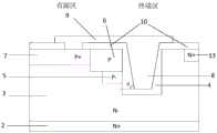
如图10所示,本例的结构为在实施例1的基础上,在沟槽4的正下方增加第二导电类型半导体材料的埋层14,可以减缓沟槽拐角处的电场集中,进一步提升耐压能力。As shown in FIG. 10, the structure of this example is based on the first embodiment, and a buried
实施例3Example 3
如图11所示,本例的结构为在实施例1的基础上,在第二导电类型注入区5正下方沿着侧壁再形成一个掺杂浓度更低的第二导电类型轻掺杂区14,可以增强JTE的效果。As shown in FIG. 11 , the structure of this example is that on the basis of
实施例4Example 4
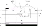
如图12所示,本例的结构为在实施例1的基础上,将沟槽4一直挖到第一导电类型半导体重掺杂区2的体内,通过增加绝缘介质层的厚度来提高耐压。As shown in FIG. 12, the structure of this example is based on the first embodiment, the
实施例5Example 5
如图13所示,本例的结构为在实施例1的基础上,取消多晶硅场板和主结7的连接,即多晶硅作为浮空场板。As shown in FIG. 13 , the structure of this example is based on
实施例6Example 6
如图14所示,本例的结构为在实施例1的基础上,源极金属11通过接触孔和多晶硅互连9相连,将源极的电位接到多晶硅场板上。As shown in FIG. 14 , the structure of this example is based on
实施例7Example 7
如图15所示,本例的结构为在实施例1的基础上,在多晶硅场板8上面淀积一层氧化层,多晶硅场板浮空。As shown in FIG. 15 , the structure of this example is based on the first embodiment, and an oxide layer is deposited on the
以上实施例中,制作器件时还可用碳化硅、砷化镓、磷化铟或锗硅等半导体材料代替体硅。In the above embodiments, semiconductor materials such as silicon carbide, gallium arsenide, indium phosphide or silicon germanium can also be used to replace bulk silicon when fabricating the device.
Claims (8)
Translated fromChineseApplications Claiming Priority (1)
| Application Number | Priority Date | Filing Date | Title |
|---|---|---|---|
| PCT/CN2016/099163WO2018049640A1 (en) | 2016-09-17 | 2016-09-17 | Folder type terminal having bulk field plate |
Publications (2)
| Publication Number | Publication Date |
|---|---|
| CN108292677A CN108292677A (en) | 2018-07-17 |
| CN108292677Btrue CN108292677B (en) | 2020-09-29 |
Family
ID=61618613
Family Applications (1)
| Application Number | Title | Priority Date | Filing Date |
|---|---|---|---|
| CN201680057871.4AExpired - Fee RelatedCN108292677B (en) | 2016-09-17 | 2016-09-17 | Folded form terminal with internal field board |
Country Status (3)
| Country | Link |
|---|---|
| US (1) | US10340332B2 (en) |
| CN (1) | CN108292677B (en) |
| WO (1) | WO2018049640A1 (en) |
Cited By (1)
| Publication number | Priority date | Publication date | Assignee | Title |
|---|---|---|---|---|
| CN113299744A (en)* | 2021-06-10 | 2021-08-24 | 珠海市浩辰半导体有限公司 | Terminal structure, semiconductor device and manufacturing method |
Families Citing this family (19)
| Publication number | Priority date | Publication date | Assignee | Title |
|---|---|---|---|---|
| CN108598151B (en)* | 2018-05-28 | 2024-02-02 | 江苏捷捷微电子股份有限公司 | Semiconductor device terminal structure capable of improving voltage endurance capability and manufacturing method thereof |
| CN109103248A (en)* | 2018-08-23 | 2018-12-28 | 深圳市南硕明泰科技有限公司 | A kind of power device terminal structure and preparation method thereof |
| CN109103260A (en)* | 2018-08-23 | 2018-12-28 | 深圳市南硕明泰科技有限公司 | Power device |
| US11158703B2 (en)* | 2019-06-05 | 2021-10-26 | Microchip Technology Inc. | Space efficient high-voltage termination and process for fabricating same |
| CN110931548A (en)* | 2019-12-16 | 2020-03-27 | 安建科技(深圳)有限公司 | Semiconductor device structure and manufacturing method thereof |
| CN112382653B (en)* | 2020-07-13 | 2024-02-23 | 电子科技大学 | Transverse variable doping terminal structure, design method and preparation method |
| CN111755504B (en)* | 2020-07-13 | 2024-02-23 | 电子科技大学 | Transverse variable doping terminal structure, design method and preparation method |
| CN113299745B (en)* | 2021-06-10 | 2022-04-15 | 珠海市浩辰半导体有限公司 | Terminal structure, semiconductor device and manufacturing method |
| CN114141858B (en)* | 2021-11-12 | 2025-06-17 | 济南晶恒电子有限责任公司 | A semiconductor terminal structure with lateral variable doping and preparation method thereof |
| CN113823679A (en)* | 2021-11-23 | 2021-12-21 | 成都蓉矽半导体有限公司 | gated diode rectifier |
| CN114335164B (en)* | 2022-01-17 | 2025-09-12 | 中国电子科技集团公司第二十四研究所 | Power semiconductor device and manufacturing method thereof |
| CN114496802B (en)* | 2022-04-14 | 2022-06-24 | 北京智芯微电子科技有限公司 | Manufacturing method of LDMOSFET device and LDMOSFET device |
| CN116190419B (en)* | 2022-12-30 | 2025-09-19 | 陕西亚成微电子股份有限公司 | Super-junction power MOSFET structure for optimizing linear output and preparation method thereof |
| CN117116974B (en)* | 2023-08-31 | 2024-08-16 | 海信家电集团股份有限公司 | Semiconductor devices |
| CN117790536B (en)* | 2023-12-26 | 2025-03-18 | 南京芯干线科技有限公司 | A junction terminal structure and preparation method thereof, and semiconductor device |
| CN118448449B (en)* | 2024-07-08 | 2024-11-19 | 无锡商甲半导体有限公司 | High-reliability IGBT device terminal structure and manufacturing method thereof |
| CN119486223B (en)* | 2024-10-30 | 2025-09-16 | 湖北九峰山实验室 | A semiconductor device terminal structure and preparation method thereof, and a semiconductor device |
| CN119317167A (en)* | 2024-12-17 | 2025-01-14 | 杭州谱析光晶半导体科技有限公司 | A terminal structure with lateral variable doping and preparation method thereof |
| CN120035189A (en)* | 2025-04-24 | 2025-05-23 | 泰科天润半导体科技(北京)有限公司 | A silicon carbide VDMOS insulated high UIS characteristic terminal and preparation method thereof |
Citations (4)
| Publication number | Priority date | Publication date | Assignee | Title |
|---|---|---|---|---|
| CN102254931A (en)* | 2011-07-14 | 2011-11-23 | 西安理工大学 | Shallow slot negative bevel terminal structure and preparation method thereof |
| CN102969358A (en)* | 2012-12-06 | 2013-03-13 | 电子科技大学 | Transverse high-voltage power semiconductor device |
| CN103022134A (en)* | 2012-12-06 | 2013-04-03 | 电子科技大学 | A SOI lateral high-voltage power device with ultra-low specific on-resistance |
| CN105932051A (en)* | 2016-07-04 | 2016-09-07 | 电子科技大学 | Grooved gate MOSFET (Metal Oxide Semiconductor Field-Effect Transistor) device |
Family Cites Families (8)
| Publication number | Priority date | Publication date | Assignee | Title |
|---|---|---|---|---|
| JP4097417B2 (en)* | 2001-10-26 | 2008-06-11 | 株式会社ルネサステクノロジ | Semiconductor device |
| DE102007061191B4 (en)* | 2007-12-17 | 2012-04-05 | Infineon Technologies Austria Ag | Semiconductor device with a semiconductor body |
| US8310001B2 (en)* | 2008-07-15 | 2012-11-13 | Maxpower Semiconductor Inc. | MOSFET switch with embedded electrostatic charge |
| CN101894865B (en) | 2009-05-21 | 2012-09-12 | 中芯国际集成电路制造(北京)有限公司 | Impact-ionization metal oxide semiconductor transistor (I-MOS) and manufacturing method thereof |
| CN103094324B (en) | 2011-11-08 | 2016-03-23 | 无锡华润上华半导体有限公司 | Trench-type insulated gate bipolar transistor and preparation method thereof |
| GB2530284A (en) | 2014-09-17 | 2016-03-23 | Anvil Semiconductors Ltd | High voltage semiconductor devices |
| CN104992976B (en)* | 2015-05-21 | 2018-03-02 | 电子科技大学 | A kind of VDMOS device and its manufacture method |
| CN105047721A (en) | 2015-08-26 | 2015-11-11 | 国网智能电网研究院 | Silicon carbide trench gate power metal-oxide-semiconductor field effect transistors (MOSFETs) device and manufacturing method thereof |
- 2016
- 2016-09-17CNCN201680057871.4Apatent/CN108292677B/ennot_activeExpired - Fee Related
- 2016-09-17WOPCT/CN2016/099163patent/WO2018049640A1/ennot_activeCeased
- 2016-09-17USUS15/774,286patent/US10340332B2/ennot_activeExpired - Fee Related
Patent Citations (4)
| Publication number | Priority date | Publication date | Assignee | Title |
|---|---|---|---|---|
| CN102254931A (en)* | 2011-07-14 | 2011-11-23 | 西安理工大学 | Shallow slot negative bevel terminal structure and preparation method thereof |
| CN102969358A (en)* | 2012-12-06 | 2013-03-13 | 电子科技大学 | Transverse high-voltage power semiconductor device |
| CN103022134A (en)* | 2012-12-06 | 2013-04-03 | 电子科技大学 | A SOI lateral high-voltage power device with ultra-low specific on-resistance |
| CN105932051A (en)* | 2016-07-04 | 2016-09-07 | 电子科技大学 | Grooved gate MOSFET (Metal Oxide Semiconductor Field-Effect Transistor) device |
Non-Patent Citations (1)
| Title |
|---|
| 高压IGBT关断状态失效的机理研究;李巍;《中国优秀硕士学位论文全文数据库信息科技辑》;20140115;35-60* |
Cited By (2)
| Publication number | Priority date | Publication date | Assignee | Title |
|---|---|---|---|---|
| CN113299744A (en)* | 2021-06-10 | 2021-08-24 | 珠海市浩辰半导体有限公司 | Terminal structure, semiconductor device and manufacturing method |
| CN113299744B (en)* | 2021-06-10 | 2022-04-15 | 珠海市浩辰半导体有限公司 | Terminal structure, semiconductor device and manufacturing method |
Also Published As
| Publication number | Publication date |
|---|---|
| US20190067415A1 (en) | 2019-02-28 |
| CN108292677A (en) | 2018-07-17 |
| WO2018049640A1 (en) | 2018-03-22 |
| US10340332B2 (en) | 2019-07-02 |
Similar Documents
| Publication | Publication Date | Title |
|---|---|---|
| CN108292677B (en) | Folded form terminal with internal field board | |
| CN107078159B (en) | semiconductor device | |
| CN106024866B (en) | A kind of groove-shaped terminal structure of power semiconductor | |
| CN106098751B (en) | A kind of power semiconductor terminal structure | |
| US9018698B2 (en) | Trench-based device with improved trench protection | |
| CN106356401B (en) | A kind of field limiting ring terminal structure of power semiconductor | |
| CN106024863A (en) | High-voltage power device terminal structure | |
| CN115513297B (en) | Silicon carbide planar MOSFET device and manufacturing method thereof | |
| TWI470802B (en) | Trench type MOS transistor crystal element and manufacturing method thereof | |
| CN105810754B (en) | A kind of metal-oxide-semiconductor diode with accumulation layer | |
| CN113937167B (en) | VDMOS device and its manufacturing method | |
| CN106057798A (en) | A MOSFET with Integrated Trench Schottky | |
| US9929285B2 (en) | Super-junction schottky diode | |
| JP3998454B2 (en) | Power semiconductor device | |
| CN102468298A (en) | Accumulation mode FET with integrated clamping circuit | |
| CN107946362A (en) | A kind of MOSFET element for improving pressure-resistant scope and preparation method thereof | |
| CN117423624A (en) | Semiconductor structure and forming method thereof | |
| CN112201686A (en) | A super junction device and terminal | |
| WO2013175880A1 (en) | Silicon carbide semiconductor device and method for manufacturing same | |
| CN106057906B (en) | A kind of accumulation type DMOS with p type buried layer | |
| CN104078517B (en) | Groove type schottky semiconductor device | |
| CN107170837A (en) | A kind of semiconductor devices and manufacture method | |
| CN114203825B (en) | A vertical silicon carbide power MOSFET device and its manufacturing method | |
| CN112909075A (en) | Trench MOSFET with charge balance structure and manufacturing method thereof | |
| CN106298976A (en) | A kind of groove-shaped Schottky diode |
Legal Events
| Date | Code | Title | Description |
|---|---|---|---|
| PB01 | Publication | ||
| PB01 | Publication | ||
| SE01 | Entry into force of request for substantive examination | ||
| SE01 | Entry into force of request for substantive examination | ||
| GR01 | Patent grant | ||
| GR01 | Patent grant | ||
| CF01 | Termination of patent right due to non-payment of annual fee | ||
| CF01 | Termination of patent right due to non-payment of annual fee | Granted publication date:20200929 Termination date:20210917 |