CN108288652B - Thin film transistor and its manufacturing method, array substrate and display panel - Google Patents
Thin film transistor and its manufacturing method, array substrate and display panelDownload PDFInfo
- Publication number
- CN108288652B CN108288652BCN201810186748.3ACN201810186748ACN108288652BCN 108288652 BCN108288652 BCN 108288652BCN 201810186748 ACN201810186748 ACN 201810186748ACN 108288652 BCN108288652 BCN 108288652B
- Authority
- CN
- China
- Prior art keywords
- channel region
- thin film
- film transistor
- layer
- present
- Prior art date
- Legal status (The legal status is an assumption and is not a legal conclusion. Google has not performed a legal analysis and makes no representation as to the accuracy of the status listed.)
- Expired - Fee Related
Links
Images


Classifications
- H—ELECTRICITY
- H10—SEMICONDUCTOR DEVICES; ELECTRIC SOLID-STATE DEVICES NOT OTHERWISE PROVIDED FOR
- H10D—INORGANIC ELECTRIC SEMICONDUCTOR DEVICES
- H10D30/00—Field-effect transistors [FET]
- H10D30/60—Insulated-gate field-effect transistors [IGFET]
- H10D30/67—Thin-film transistors [TFT]
- G—PHYSICS
- G02—OPTICS
- G02F—OPTICAL DEVICES OR ARRANGEMENTS FOR THE CONTROL OF LIGHT BY MODIFICATION OF THE OPTICAL PROPERTIES OF THE MEDIA OF THE ELEMENTS INVOLVED THEREIN; NON-LINEAR OPTICS; FREQUENCY-CHANGING OF LIGHT; OPTICAL LOGIC ELEMENTS; OPTICAL ANALOGUE/DIGITAL CONVERTERS
- G02F1/00—Devices or arrangements for the control of the intensity, colour, phase, polarisation or direction of light arriving from an independent light source, e.g. switching, gating or modulating; Non-linear optics
- G02F1/01—Devices or arrangements for the control of the intensity, colour, phase, polarisation or direction of light arriving from an independent light source, e.g. switching, gating or modulating; Non-linear optics for the control of the intensity, phase, polarisation or colour
- G02F1/13—Devices or arrangements for the control of the intensity, colour, phase, polarisation or direction of light arriving from an independent light source, e.g. switching, gating or modulating; Non-linear optics for the control of the intensity, phase, polarisation or colour based on liquid crystals, e.g. single liquid crystal display cells
- G02F1/133—Constructional arrangements; Operation of liquid crystal cells; Circuit arrangements
- G02F1/136—Liquid crystal cells structurally associated with a semi-conducting layer or substrate, e.g. cells forming part of an integrated circuit
- G02F1/1362—Active matrix addressed cells
- G02F1/1368—Active matrix addressed cells in which the switching element is a three-electrode device
- H—ELECTRICITY
- H10—SEMICONDUCTOR DEVICES; ELECTRIC SOLID-STATE DEVICES NOT OTHERWISE PROVIDED FOR
- H10D—INORGANIC ELECTRIC SEMICONDUCTOR DEVICES
- H10D30/00—Field-effect transistors [FET]
- H10D30/01—Manufacture or treatment
- H10D30/021—Manufacture or treatment of FETs having insulated gates [IGFET]
- H10D30/031—Manufacture or treatment of FETs having insulated gates [IGFET] of thin-film transistors [TFT]
- H—ELECTRICITY
- H10—SEMICONDUCTOR DEVICES; ELECTRIC SOLID-STATE DEVICES NOT OTHERWISE PROVIDED FOR
- H10D—INORGANIC ELECTRIC SEMICONDUCTOR DEVICES
- H10D86/00—Integrated devices formed in or on insulating or conducting substrates, e.g. formed in silicon-on-insulator [SOI] substrates or on stainless steel or glass substrates
- H10D86/40—Integrated devices formed in or on insulating or conducting substrates, e.g. formed in silicon-on-insulator [SOI] substrates or on stainless steel or glass substrates characterised by multiple TFTs
- H10D86/60—Integrated devices formed in or on insulating or conducting substrates, e.g. formed in silicon-on-insulator [SOI] substrates or on stainless steel or glass substrates characterised by multiple TFTs wherein the TFTs are in active matrices
Landscapes
- Physics & Mathematics (AREA)
- Nonlinear Science (AREA)
- Engineering & Computer Science (AREA)
- Microelectronics & Electronic Packaging (AREA)
- Mathematical Physics (AREA)
- Chemical & Material Sciences (AREA)
- Crystallography & Structural Chemistry (AREA)
- General Physics & Mathematics (AREA)
- Optics & Photonics (AREA)
- Thin Film Transistor (AREA)
Abstract
Translated fromChinese
Description
Translated fromChinese技术领域technical field
本发明涉及显示技术领域,具体涉及一种薄膜晶体管及其制造方法、阵列基板和显示面板。The present invention relates to the field of display technology, in particular to a thin film transistor and a manufacturing method thereof, an array substrate and a display panel.
背景技术Background technique
在平板显示技术领域,薄膜晶体管液晶显示器(Thin Film Transistor LiquidCrystal Display,TFT-LCD)具有体积小、功耗低、无辐射以及制作成本相对较低等特点,越来越多地被应用于高性能显示领域当中。TFT-LCD的主体结构包括对盒的阵列基板和彩膜基板,阵列基板包括矩阵排列的多个像素单元,像素单元由多条栅线和多条数据线垂直交叉限定,薄膜晶体管设置在栅线与数据线的交叉位置。In the field of flat panel display technology, Thin Film Transistor Liquid Crystal Display (TFT-LCD) has the characteristics of small size, low power consumption, no radiation and relatively low production cost, and is increasingly used in high-performance displayed in the field. The main structure of the TFT-LCD includes a cell-aligned array substrate and a color filter substrate. The array substrate includes a plurality of pixel units arranged in a matrix. The pixel unit is defined by a plurality of gate lines and a plurality of data lines that intersect vertically. The thin film transistors are arranged on the gate lines. The intersection with the data line.
薄膜晶体管包括栅电极、有源层、源电极和漏电极,其中,有源层包括与源电极接触的源区、与漏电极接触的漏区、以及位于源区与漏区之间的沟道区。当薄膜晶体管处于打开状态时,有源层的沟道区从半导体状态变为导体状态,形成导电沟道。The thin film transistor includes a gate electrode, an active layer, a source electrode and a drain electrode, wherein the active layer includes a source region in contact with the source electrode, a drain region in contact with the drain electrode, and a channel between the source region and the drain region Area. When the thin film transistor is in an on state, the channel region of the active layer changes from a semiconductor state to a conductor state, forming a conductive channel.
漏电流(Ioff)特性是薄膜晶体管的一个重要参数,若其过大,则影响薄膜晶体管的开关特性,从而导致TFT-LCD的显示画面出现显示不均、发白、发灰、污渍、串扰(crosstalk)等缺陷。目前,现有技术通常采用减小沟道宽长比来减小薄膜晶体管的漏电流,但减小沟道宽长比会降低薄膜晶体管的开启电流(Ion),使得现有降低薄膜晶体管漏电流的解决方案效果不理想。The leakage current (Ioff) characteristic is an important parameter of the thin film transistor. If it is too large, it will affect the switching characteristics of the thin film transistor, resulting in uneven display, whitening, graying, stains, crosstalk ( crosstalk) and other defects. At present, in the prior art, reducing the channel width to length ratio is usually used to reduce the leakage current of the thin film transistor. However, reducing the channel width to length ratio will reduce the on-current (Ion) of the thin film transistor, so that the leakage current of the thin film transistor can be reduced in the prior art. The solution does not work well.
因此,如何有效降低薄膜晶体管的漏电流,是本领域亟待解决的技术问题。Therefore, how to effectively reduce the leakage current of the thin film transistor is a technical problem to be solved urgently in the art.
发明内容SUMMARY OF THE INVENTION
本发明实施例所要解决的技术问题是,提供一种薄膜晶体管及其制造方法、阵列基板和显示面板,以有效降低薄膜晶体管的漏电流。The technical problem to be solved by the embodiments of the present invention is to provide a thin film transistor and a manufacturing method thereof, an array substrate and a display panel, so as to effectively reduce the leakage current of the thin film transistor.
为了解决上述技术问题,本发明实施例提供了一种薄膜晶体管的制备方法,包括:In order to solve the above technical problems, an embodiment of the present invention provides a method for preparing a thin film transistor, including:
形成薄膜晶体管的沟道区;forming a channel region of a thin film transistor;
对所述沟道区进行处理,在所述沟道区表面形成空穴层。The channel region is processed to form a hole layer on the surface of the channel region.
可选地,对所述沟道区进行处理,在所述沟道区表面形成空穴层,包括:Optionally, the channel region is processed to form a hole layer on the surface of the channel region, including:
在化学气相沉积设备中,采用硼烷等离子体对所述沟道区表面进行处理,在所述沟道区表面形成带正电荷空穴的空穴层。In the chemical vapor deposition equipment, borane plasma is used to treat the surface of the channel region to form a hole layer with positively charged holes on the surface of the channel region.
可选地,所述空穴层的厚度为0.1nm~1.0nm。Optionally, the thickness of the hole layer is 0.1 nm˜1.0 nm.
可选地,所述硼烷等离子体的气体流量为100sccm~500sccm,气体压强为50Pa~200Pa,处理时间为10s~50s。Optionally, the gas flow rate of the borane plasma is 100sccm-500sccm, the gas pressure is 50Pa-200Pa, and the processing time is 10s-50s.
可选地,沟道区表面与化学气相沉积设备的电极间距为50mm~300mm,化学气相沉积设备的功率为1000W~8000W,电流为5A~50A。Optionally, the distance between the surface of the channel region and the electrode of the chemical vapor deposition equipment is 50mm-300mm, the power of the chemical vapor deposition equipment is 1000W-8000W, and the current is 5A-50A.
为了解决上述技术问题,本发明实施例还提供了一种薄膜晶体管,包括沟道区,所述沟道区表面形成有空穴层。In order to solve the above technical problem, an embodiment of the present invention further provides a thin film transistor, which includes a channel region, and a hole layer is formed on the surface of the channel region.
可选地,所述空穴层的厚度为0.1nm~1.0nm。Optionally, the thickness of the hole layer is 0.1 nm˜1.0 nm.
可选地,所述空穴层中形成有带正电荷的空穴。Optionally, positively charged holes are formed in the hole layer.
本发明实施例还提供了一种阵列基板,包括前述的薄膜晶体管。Embodiments of the present invention also provide an array substrate including the aforementioned thin film transistor.
本发明实施例还提供了一种显示面板,包括前述的阵列基板。Embodiments of the present invention also provide a display panel, including the aforementioned array substrate.
本发明实施例所提供的薄膜晶体管及其制造方法、阵列基板和显示面板,通过在沟道区表面形成空穴层,空穴层利用其中带正电荷的空穴与迁移至沟道区表面的电子复合,避免了沟道区表面可能形成的电流通道,有效降低了漏电流,改善了薄膜晶体管特性。In the thin film transistor and its manufacturing method, the array substrate and the display panel provided by the embodiments of the present invention, a hole layer is formed on the surface of the channel region, and the hole layer utilizes the positively charged holes therein and the holes that migrate to the surface of the channel region. The electron recombination avoids the current channel that may be formed on the surface of the channel region, effectively reduces the leakage current, and improves the characteristics of the thin film transistor.
当然,实施本发明的任一产品或方法并不一定需要同时达到以上所述的所有优点。本发明的其它特征和优点将在随后的说明书实施例中阐述,并且,部分地从说明书实施例中变得显而易见,或者通过实施本发明而了解。本发明实施例的目的和其他优点可通过在说明书、权利要求书以及附图中所特别指出的结构来实现和获得。Of course, it is not necessary for any product or method of the present invention to achieve all of the advantages described above at the same time. Other features and advantages of the present invention will be set forth in the description examples which follow, and, in part, will be apparent from the description examples, or may be learned by practice of the invention. The objectives and other advantages of the embodiments of the invention may be realized and attained by the structure particularly pointed out in the description, claims and drawings.
附图说明Description of drawings
附图用来提供对本发明技术方案的进一步理解,并且构成说明书的一部分,与本申请的实施例一起用于解释本发明的技术方案,并不构成对本发明技术方案的限制。附图中各部件的形状和大小不反映真实比例,目的只是示意说明本发明内容。The accompanying drawings are used to provide a further understanding of the technical solutions of the present invention, and constitute a part of the specification. They are used to explain the technical solutions of the present invention together with the embodiments of the present application, and do not limit the technical solutions of the present invention. The shapes and sizes of the components in the drawings do not reflect the actual scale, and are only intended to illustrate the content of the present invention.
图1为本发明薄膜晶体管的制备方法的流程图;Fig. 1 is the flow chart of the preparation method of the thin film transistor of the present invention;
图2为本发明第一实施例形成栅结构层图案后的示意图;FIG. 2 is a schematic diagram after forming a gate structure layer pattern according to the first embodiment of the present invention;
图3为本发明第一实施例形成有源层图案后的示意图;FIG. 3 is a schematic diagram after forming an active layer pattern according to the first embodiment of the present invention;
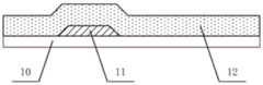
图4为本发明第一实施例形成源电极和漏电极图案后的示意图;FIG. 4 is a schematic diagram after forming source electrode and drain electrode patterns according to the first embodiment of the present invention;
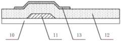
图5为本发明第一实施例进行沟道区表面处理后的示意图;FIG. 5 is a schematic diagram after the surface treatment of the channel region is performed according to the first embodiment of the present invention;
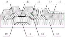
图6为本发明第二实施例形成钝化层图案后的示意图;FIG. 6 is a schematic diagram after the passivation layer pattern is formed according to the second embodiment of the present invention;
图7为本发明第二实施例形成像素电极图案后的示意图。FIG. 7 is a schematic diagram after forming a pixel electrode pattern according to the second embodiment of the present invention.
附图标记说明:Explanation of reference numbers:
10—基底; 11—栅电极; 12—栅绝缘层;10—substrate; 11—gate electrode; 12—gate insulating layer;
13—有源层; 14—源电极; 15—漏电极;13—active layer; 14—source electrode; 15—drain electrode;
16—钝化层; 17—像素电极; 20—空穴层。16—passivation layer; 17—pixel electrode; 20—hole layer.
具体实施方式Detailed ways
下面结合附图和实施例对本发明的具体实施方式作进一步详细描述。以下实施例用于说明本发明,但不用来限制本发明的范围。需要说明的是,在不冲突的情况下,本申请中的实施例及实施例中的特征可以相互任意组合。The specific embodiments of the present invention will be described in further detail below with reference to the accompanying drawings and examples. The following examples are intended to illustrate the present invention, but not to limit the scope of the present invention. It should be noted that, the embodiments in the present application and the features in the embodiments may be arbitrarily combined with each other if there is no conflict.
经本申请发明人研究发现,对传统沟道区刻蚀型薄膜晶体管,形成漏电流Ioff的原因是:由于沟道区表面在刻蚀中受到等离子的损伤,当薄膜晶体管处于关闭状态时,电子受到电场的影响会全部迁移至沟道区表面,此时若源电极与漏电极之间存在电压差,迁移至沟道区表面的电子就会构成电流通道,从而形成漏电流Ioff。The inventors of the present application found that the reason for the formation of the leakage current Ioff for the traditional channel region etched thin film transistor is: because the surface of the channel region is damaged by plasma during etching, when the thin film transistor is in the off state, electrons Under the influence of the electric field, they will all migrate to the surface of the channel region. At this time, if there is a voltage difference between the source electrode and the drain electrode, the electrons migrated to the surface of the channel region will form a current channel, thereby forming a leakage current Ioff.
下面通过具体实施例详细说明本发明实施例的技术方案。The technical solutions of the embodiments of the present invention are described in detail below through specific embodiments.
第一实施例first embodiment
为了有效降低薄膜晶体管的漏电流,本实施例提供了一种在沟道区表面形成空穴层的解决方案。图1为本发明薄膜晶体管的制备方法的流程图,如图1所示,薄膜晶体管的制备方法包括:In order to effectively reduce the leakage current of the thin film transistor, this embodiment provides a solution for forming a hole layer on the surface of the channel region. 1 is a flow chart of a method for preparing a thin film transistor of the present invention. As shown in FIG. 1 , the method for preparing a thin film transistor includes:
S1、形成薄膜晶体管的沟道区;S1, forming the channel region of the thin film transistor;
S2、对所述沟道区进行处理,在所述沟道区表面形成空穴层。S2, processing the channel region to form a hole layer on the surface of the channel region.
本发明实施例所提供的薄膜晶体管的制备方法,通过在沟道区表面形成空穴层,空穴层利用其中带正电荷的空穴与迁移至沟道区表面的电子复合,避免了沟道区表面可能形成的电流通道,有效降低了漏电流,改善了薄膜晶体管特性。In the preparation method of the thin film transistor provided by the embodiment of the present invention, a hole layer is formed on the surface of the channel region, and the hole layer utilizes the positively charged holes therein to recombine with the electrons migrated to the surface of the channel region, thereby avoiding the channel The current channel that may be formed on the surface of the region effectively reduces the leakage current and improves the characteristics of the thin film transistor.
其中,步骤S2包括:在化学气相沉积设备中,采用硼烷等离子体对所述沟道区表面进行处理,在所述沟道区表面形成带正电荷空穴的空穴层。优选地,所述空穴层的厚度为0.1nm~1.0nm。Wherein, step S2 includes: in a chemical vapor deposition apparatus, using borane plasma to process the surface of the channel region, and forming a hole layer with positively charged holes on the surface of the channel region. Preferably, the thickness of the hole layer is 0.1 nm˜1.0 nm.
对所述沟道区表面进行处理时,硼烷等离子体的气体流量为100sccm~500sccm,气体压强为50Pa~200Pa,处理时间为10s~50s。When processing the surface of the channel region, the gas flow rate of the borane plasma is 100sccm-500sccm, the gas pressure is 50Pa-200Pa, and the processing time is 10s-50s.
对所述沟道区表面进行处理时,沟道区表面与化学气相沉积设备的电极间距为50mm~300mm,化学气相沉积设备的功率为1000W~8000W,电流为5A~50A。When processing the surface of the channel region, the electrode distance between the surface of the channel region and the chemical vapor deposition equipment is 50mm-300mm, the power of the chemical vapor deposition equipment is 1000W-8000W, and the current is 5A-50A.
下面通过薄膜晶体管的制备过程进一步说明本实施例的技术方案。The technical solution of this embodiment is further described below through the preparation process of the thin film transistor.
图2~图7为本发明第一实施例制备薄膜晶体管的示意图。其中,本发明实施例中所说的“构图工艺”包括沉积膜层、涂覆光刻胶、掩模曝光、显影、刻蚀、剥离光刻胶等处理,是现有成熟的制备工艺。沉积可采用溅射、蒸镀、化学气相沉积等已知工艺,涂覆可采用已知的涂覆工艺,刻蚀可采用已知的方法,在此不做具体的限定。FIG. 2 to FIG. 7 are schematic diagrams of preparing a thin film transistor according to the first embodiment of the present invention. Among them, the "patterning process" mentioned in the embodiments of the present invention includes deposition of film layer, coating of photoresist, mask exposure, development, etching, stripping of photoresist, etc., which is a mature preparation process. The deposition can use known processes such as sputtering, evaporation, and chemical vapor deposition, the coating can use a known coating process, and the etching can use a known method, which is not specifically limited here.
第一次构图工艺中,在基底上通过构图工艺形成栅结构层,其中栅结构层包括栅电极、栅线(未示出)和栅绝缘层。形成栅结构层包括:在基底10上沉积栅金属薄膜,涂覆一层光刻胶,采用单色调掩膜版对光刻胶进行曝光显影,对栅金属薄膜进行刻蚀并剥离剩余的光刻胶,形成栅电极11和栅线(未示出)图案,随后沉积栅绝缘层12,如图2所示。其中,栅金属薄膜可以采用铜、铝、钼等金属,或者铜、铝、钼任意两个或多个膜层组成的复合膜层,厚度为100nm~1000nm,通过磁控溅射(Sputter)方式沉积。光刻胶可以采用正性光刻胶,厚度为1μm~4μm,被曝光的光刻胶与显影液反应,被掩膜版遮挡的光刻胶保留下来。刻蚀可以采用湿法刻蚀,将完成曝光显影的衬底置于刻蚀液中进行刻蚀,刻蚀液的主要成分为磷酸、醋酸、硝酸和水等,刻蚀温度为40℃~80℃,刻蚀时间为40s~80s。栅绝缘层可以采用氧化硅SiOx或氮化硅SiNx,或氧化硅、氮氧化硅、氮化硅任意两个或多个膜层组成的复合膜层。In the first patterning process, a gate structure layer is formed on the substrate through a patterning process, wherein the gate structure layer includes a gate electrode, a gate line (not shown) and a gate insulating layer. Forming the gate structure layer includes: depositing a gate metal film on the
第二次构图工艺中,在形成有栅结构层的基底上,通过构图工艺形成有源层图案。形成有源层图案包括:在形成有栅结构层的基底上,沉积有源层薄膜,涂覆一层光刻胶,采用单色调掩膜版对光刻胶进行曝光显影,对有源层薄膜进行刻蚀并剥离剩余的光刻胶,形成有源层13图案,如图3所示。其中,有源层薄膜可以采用硅半导体材料。In the second patterning process, an active layer pattern is formed by a patterning process on the substrate on which the gate structure layer is formed. Forming the active layer pattern includes: depositing an active layer film on a substrate formed with a gate structure layer, coating a layer of photoresist, exposing and developing the photoresist by using a single-tone mask, and exposing the active layer film Etching is performed and the remaining photoresist is stripped to form a pattern of the
第三次构图工艺中,在形成有有源层图案的基底上,通过构图工艺形成源电极和漏电极图案。形成源电极和漏电极图案包括:在形成有前述结构图案的基底上,沉积源漏金属薄膜,涂覆一层光刻胶,采用单色调掩膜版对光刻胶进行曝光显影,对源漏金属薄膜进行刻蚀并剥离剩余的光刻胶,形成源电极14、漏电极15、数据线(未示出)和沟道区图案,如图4所示。其中,源电极14与有源层13的一端接触形成源区,漏电极15与有源层13的另一端接触形成漏区,源电极14与漏电极15之间形成沟道区。源漏金属薄膜可以采用铜、铝、钼等金属,厚度为100nm~1000nm,通过磁控溅射(Sputter)方式沉积。In the third patterning process, source electrode and drain electrode patterns are formed on the substrate on which the active layer pattern is formed through a patterning process. Forming the source electrode and drain electrode patterns includes: depositing a source-drain metal film on the substrate formed with the aforementioned structural pattern, coating a layer of photoresist, and exposing and developing the photoresist by using a monochromatic mask, and analysing the source and drain electrodes. The metal film is etched and the remaining photoresist is stripped to form
在实际制备中,第三次构图工艺可以采用先湿刻后干刻的方式形成沟道区图案,即先采用湿刻设备形成源电极14、漏电极15和数据线图案,然后转移至干刻设备进行沟道区刻蚀。在完成沟道区刻蚀后,进行沟道区表面处理。沟道区表面处理包括:将完成沟道区刻蚀的衬底置于化学气相沉积(Chemical Vapor Deposition,CVD)设备中,采用硼烷(B2H6)等离子体对沟道区表面进行处理。表面处理中,CVD设备中的硼烷被电离成等离子体,随后以类似离子注入的方式注入到沟道区表面形成空穴层,硼烷B2H6气体流量为100sccm~500sccm,气体压强为50Pa~200Pa,处理时间为10s~50s。表面处理采用的化学气相沉积设备,功率为1000W~8000W,电流为5A~50A,并控制沟道区表面与化学气相沉积设备的电极间距为50mm~300mm。硼烷等离子体处理中,使部分硼原子从沟道区表面进入有源层内部,进入有源层内部的硼原子与有源层中的硅原子成键形成空穴单元,在有源层表面形成带正电荷空穴的空穴层20,空穴层20的厚度为0.1nm~1.0nm,如图5所示。本发明实施例中,沟道区表面经过硼烷等离子体处理,还可以弥补刻蚀沟道区造成表面缺陷,使得在薄膜晶体管处于关闭状态时,电子迁移至沟道区表面的数量减少。In actual preparation, the third patterning process can use wet etching first and then dry etching to form the channel region pattern, that is, first use wet etching equipment to form
本实施例提供了一种背沟道刻蚀型薄膜晶体管的制备方法,在完成沟道区刻蚀后,通过对沟道区表面进行硼烷等离子体处理,使进入有源层内部的硼原子与有源层中的硅成键形成带正电荷的空穴单元,在沟道区表面形成带正电荷空穴的空穴层。在薄膜晶体管处于关闭状态,当电子迁移至空穴层时,迁移的电子与空穴层的空穴复合,即使源电极与漏电极之间存在电压差,沟道区表面也不会形成电流通道。进一步地,沟道区表面经过硼烷等离子体处理,还弥补了刻蚀沟道区造成表面缺陷,使得在薄膜晶体管处于关闭状态时,电子迁移至有源层表面的数量减少,进一步降低了沟道区表面形成电流通道的几率。因此,本实施例有效降低了薄膜晶体管的漏电流,有效改善了薄膜晶体管特性。This embodiment provides a method for preparing a back-channel etched thin film transistor. After the etching of the channel region is completed, borane plasma treatment is performed on the surface of the channel region, so that the boron atoms entering the inside of the active layer are It forms bonds with silicon in the active layer to form positively charged hole units, and forms a positively charged hole layer on the surface of the channel region. When the thin film transistor is in the off state, when the electrons migrate to the hole layer, the migrated electrons recombine with the holes of the hole layer. Even if there is a voltage difference between the source electrode and the drain electrode, no current channel will be formed on the surface of the channel region. . Further, the borane plasma treatment on the surface of the channel region also compensates for the surface defects caused by etching the channel region, so that when the thin film transistor is in the off state, the number of electrons that migrate to the surface of the active layer is reduced, which further reduces the channel region. The probability of forming a current channel on the surface of the channel region. Therefore, the present embodiment effectively reduces the leakage current of the thin film transistor and effectively improves the characteristics of the thin film transistor.
第二实施例Second Embodiment
基于本发明实施例的技术构思,本发明实施例还提供了一种薄膜晶体管,采用前述第一实施例薄膜晶体管的制备方法制备。如图5所示,本实施例薄膜晶体管包括:Based on the technical concept of the embodiment of the present invention, the embodiment of the present invention further provides a thin film transistor, which is prepared by the method for preparing the thin film transistor of the first embodiment. As shown in FIG. 5 , the thin film transistor of this embodiment includes:
基底10;
设置在基底10上的栅电极11;the
覆盖栅电极11的栅绝缘层12;a
设置在栅绝缘层12上的有源层13;an
设置在有源层13上的源电极14和漏电极15,源电极14与漏电极15之间形成沟道区,且所述沟道区表面形成有空穴层20。The
其中,空穴层20的厚度为0.1nm~1.0nm,空穴层20中形成有带正电荷的空穴,空穴层20是采用硼烷等离子体对所述沟道区表面进行处理形成的,空穴层20中带正电荷空穴是通过硼烷B2H6等离子体处理使硼原子进入沟道区的有源层与有源层中的硅成键形成。The thickness of the
其中,栅电极11、源电极14和漏电极15的材料可以采用铜、铝、钼等金属,或者铜、铝、钼任意两个或多个膜层组成的复合膜层,栅绝缘层11的材料可以采用氧化硅SiOx或氮化硅SiNx,或氧化硅、氮氧化硅、氮化硅任意两个或多个膜层组成的复合膜层,有源层的材料可以采用硅半导体。The materials of the
本实施例提供了薄膜晶体管,由于沟道区表面形成有带正电荷空穴单元的空穴层,有效降低了薄膜晶体管的漏电流,有效改善了薄膜晶体管特性。第三实施例This embodiment provides a thin film transistor. Since a hole layer with positively charged hole units is formed on the surface of the channel region, the leakage current of the thin film transistor is effectively reduced, and the characteristics of the thin film transistor are effectively improved. Third Embodiment
基于本发明实施例的技术构思,本发明实施例还提供了一种阵列基板及其制备方法。本实施例阵列基板的制备方法包括:Based on the technical concept of the embodiments of the present invention, the embodiments of the present invention further provide an array substrate and a method for manufacturing the same. The preparation method of the array substrate in this embodiment includes:
第一次~第三次构图工艺与前述第一实施例相同。The first to third patterning processes are the same as the aforementioned first embodiment.
第四次构图工艺中,在形成有前述结构图案的基底上,通过构图工艺形成钝化层图案。形成钝化层图案包括:在形成有前述结构图案的基底上,沉积钝化层薄膜,涂覆一层光刻胶,采用单色调掩膜版对光刻胶进行曝光显影,对钝化层薄膜进行刻蚀并剥离剩余的光刻胶,形成带有过孔的钝化层16,过孔位于漏电极15位置,过孔中暴露出漏电极15表面,如图6所示。其中,钝化层薄膜可以采用氧化硅、氮化硅或氮氧化硅,或氧化硅、氮氧化硅、氮化硅任意两个或多个膜层组成的复合膜层。In the fourth patterning process, a passivation layer pattern is formed through a patterning process on the substrate on which the aforementioned structural pattern is formed. Forming the passivation layer pattern includes: depositing a passivation layer film on the substrate formed with the aforementioned structural pattern, coating a layer of photoresist, using a single-tone mask to expose and develop the photoresist, and exposing the passivation layer film Etching is performed and the remaining photoresist is stripped to form a
第五次构图工艺中,在形成有前述结构图案的基底上,通过构图工艺形成像素电极图案。形成像素电极图案包括:在形成有前述结构图案的基底上,沉积透明导电薄膜,涂覆一层光刻胶,采用单色调掩膜版对光刻胶进行曝光显影,对透明导电薄膜进行刻蚀并剥离剩余的光刻胶,形成像素电极17图案,像素电极17通过过孔与漏电极15连接,如图7所示。其中,透明导电薄膜可以采用氧化铟锡ITO或氧化铟锌IZO。In the fifth patterning process, pixel electrode patterns are formed on the substrate on which the aforementioned structural patterns are formed through a patterning process. Forming the pixel electrode pattern includes: depositing a transparent conductive film on the substrate formed with the aforementioned structural pattern, coating a layer of photoresist, using a single-tone mask to expose and develop the photoresist, and etch the transparent conductive film The remaining photoresist is peeled off to form a pattern of the
采用前述阵列基板的制备方法制备的阵列基板包括:The array substrate prepared by the aforementioned preparation method of the array substrate includes:
基底10;
设置在基底10上的栅电极11;the
覆盖栅电极11的栅绝缘层12;a
设置在栅绝缘层12上的有源层13;an
设置在有源层13上的源电极14和漏电极15,源电极14与漏电极15之间形成沟道区,且所述沟道区表面形成有空穴层20;The
覆盖源电极14、漏电极15和沟道区的钝化层16,钝化层16上开设有过孔,过孔暴露出漏电极15的表面;A
设置在钝化层16上的像素电极17,像素电极17通过过孔与漏电极15连接。The
其中,钝化层16的材料可以采用氧化硅SiOx或氮化硅SiNx,或氧化硅、氮氧化硅、氮化硅任意两个或多个膜层组成的复合膜层,像素电极17的材料可以采用ITO或IZO。Wherein, the material of the
本实例中与前述实施例相同,有效降低了薄膜晶体管的漏电流,有效改善了薄膜晶体管特性。In this example, the leakage current of the thin film transistor is effectively reduced, and the characteristics of the thin film transistor are effectively improved, as in the previous embodiment.
需要说明的是,虽然前面以五次构图工艺为例对薄膜晶体管和阵列基板的结构进行了说明,但实际实施时,还可以采用其它构图工艺,本发明在此不做具体限制。例如,薄膜晶体管采用二次构图工艺或阵列基板采用四次构图工艺制备,将第二次构图工艺和第三次构图工艺合并成一个使用半色调掩膜版或灰色调掩膜版的构图工艺。具体包括:在栅绝缘层上依次沉积有源层薄膜和源漏金属薄膜,在源漏金属薄膜上涂覆一层光刻胶,采用半色调掩膜版或灰色调掩膜版对光刻胶进行阶梯曝光并显影,在源电极、漏电极和数据线图案位置形成未曝光区域,具有第一厚度的光刻胶,在沟道区图案位置形成部分曝光区域,具有第二厚度的光刻胶,在其余位置形成完全曝光区域,无光刻胶,第一厚度大于第二厚度。通过第一次刻蚀工艺刻蚀掉完全曝光区域的源漏金属薄膜和有源层薄膜,进行光刻胶灰化处理,使光刻胶在整体上去除第二厚度,暴露出部分曝光区域的源漏金属薄膜,通过第二次刻蚀工艺刻蚀掉部分曝光区域的源漏金属薄膜,剥离掉剩余的光刻胶,形成有源层、源电极、漏电极和沟道区图案。It should be noted that although the structure of the thin film transistor and the array substrate is described by taking five patterning processes as an example, in actual implementation, other patterning processes can also be used, which is not specifically limited in the present invention. For example, the thin film transistor is fabricated by a second patterning process or the array substrate is prepared by a fourth patterning process, and the second patterning process and the third patterning process are combined into one patterning process using a half-tone mask or a gray-tone mask. Specifically, it includes: sequentially depositing an active layer film and a source-drain metal film on the gate insulating layer, coating a layer of photoresist on the source-drain metal film, and using a half-tone mask or a gray-tone mask to adjust the photoresist Step exposure and development are performed to form an unexposed area at the pattern position of the source electrode, the drain electrode and the data line with a photoresist of a first thickness, and a partially exposed area is formed at the pattern position of the channel region with a photoresist of a second thickness , forming a fully exposed area in the remaining positions, without photoresist, and the first thickness is greater than the second thickness. The source-drain metal film and the active layer film in the fully exposed area are etched away by the first etching process, and the photoresist is ashed to remove the second thickness of the photoresist as a whole, exposing the partially exposed area. For the source-drain metal film, the source-drain metal film in the partially exposed area is etched away by the second etching process, and the remaining photoresist is peeled off to form the pattern of the active layer, the source electrode, the drain electrode and the channel region.
需要说明的是,虽然前面以底栅型结构对薄膜晶体管和阵列基板的结构进行了说明,但实际实施时,本发明也可以适用于顶栅型结构。It should be noted that although the structures of the thin film transistor and the array substrate are described above with a bottom-gate structure, in actual implementation, the present invention can also be applied to a top-gate structure.
第四实施例Fourth Embodiment
本发明实施例还提供了一种显示面板,包括前述第二实施例的薄膜晶体管,或包括前述第三实施例的阵列基板。显示装置可以是LCD显示面板,也可以是有机发光二极管(Organic Light-Emitting Diode,OLED)显示面板等。显示面板可以为:手机、平板电脑、电视机、显示器、笔记本电脑、数码相框、导航仪等任何具有显示功能的产品或部件。An embodiment of the present invention further provides a display panel including the thin film transistor of the second embodiment, or the array substrate of the third embodiment. The display device may be an LCD display panel or an organic light-emitting diode (Organic Light-Emitting Diode, OLED) display panel or the like. The display panel can be any product or component with a display function, such as a mobile phone, a tablet computer, a TV, a monitor, a notebook computer, a digital photo frame, and a navigator.
在本发明实施例的描述中,需要理解的是,术语“中部”、“上”、“下”、“前”、“后”、“竖直”、“水平”、“顶”、“底”“内”、“外”等指示的方位或位置关系为基于附图所示的方位或位置关系,仅是为了便于描述本发明和简化描述,而不是指示或暗示所指的装置或元件必须具有特定的方位、以特定的方位构造和操作,因此不能理解为对本发明的限制。In the description of the embodiments of the present invention, it should be understood that the terms "middle", "upper", "lower", "front", "rear", "vertical", "horizontal", "top", "bottom" "The orientation or positional relationship indicated by "inside", "outside", etc. is based on the orientation or positional relationship shown in the drawings, and is only for the convenience of describing the present invention and simplifying the description, rather than indicating or implying that the indicated device or element must be It has a specific orientation, is constructed and operates in a specific orientation, and therefore should not be construed as a limitation of the present invention.
在本发明实施例的描述中,需要说明的是,除非另有明确的规定和限定,术语“安装”、“相连”、“连接”应做广义理解,例如,可以是固定连接,也可以是可拆卸连接,或一体地连接;可以是机械连接,也可以是电连接;可以是直接相连,也可以通过中间媒介间接相连,可以是两个元件内部的连通。对于本领域的普通技术人员而言,可以具体情况理解上述术语在本发明中的具体含义。In the description of the embodiments of the present invention, it should be noted that the terms "installed", "connected" and "connected" should be understood in a broad sense, unless otherwise expressly specified and limited. For example, it may be a fixed connection or a Removable connection, or integral connection; can be mechanical connection, can also be electrical connection; can be directly connected, can also be indirectly connected through an intermediate medium, can be internal communication between two components. For those of ordinary skill in the art, the specific meanings of the above terms in the present invention can be understood in specific situations.
虽然本发明所揭露的实施方式如上,但所述的内容仅为便于理解本发明而采用的实施方式,并非用以限定本发明。任何本发明所属领域内的技术人员,在不脱离本发明所揭露的精神和范围的前提下,可以在实施的形式及细节上进行任何的修改与变化,但本发明的专利保护范围,仍须以所附的权利要求书所界定的范围为准。Although the embodiments disclosed in the present invention are as above, the described contents are only the embodiments adopted to facilitate the understanding of the present invention, and are not intended to limit the present invention. Any person skilled in the art to which the present invention belongs, without departing from the spirit and scope disclosed by the present invention, can make any modifications and changes in the form and details of the implementation, but the scope of the patent protection of the present invention still needs to be The scope defined by the appended claims shall prevail.
Claims (6)
Priority Applications (1)
| Application Number | Priority Date | Filing Date | Title |
|---|---|---|---|
| CN201810186748.3ACN108288652B (en) | 2018-03-07 | 2018-03-07 | Thin film transistor and its manufacturing method, array substrate and display panel |
Applications Claiming Priority (1)
| Application Number | Priority Date | Filing Date | Title |
|---|---|---|---|
| CN201810186748.3ACN108288652B (en) | 2018-03-07 | 2018-03-07 | Thin film transistor and its manufacturing method, array substrate and display panel |
Publications (2)
| Publication Number | Publication Date |
|---|---|
| CN108288652A CN108288652A (en) | 2018-07-17 |
| CN108288652Btrue CN108288652B (en) | 2020-12-01 |
Family
ID=62833056
Family Applications (1)
| Application Number | Title | Priority Date | Filing Date |
|---|---|---|---|
| CN201810186748.3AExpired - Fee RelatedCN108288652B (en) | 2018-03-07 | 2018-03-07 | Thin film transistor and its manufacturing method, array substrate and display panel |
Country Status (1)
| Country | Link |
|---|---|
| CN (1) | CN108288652B (en) |
Families Citing this family (1)
| Publication number | Priority date | Publication date | Assignee | Title |
|---|---|---|---|---|
| CN109003940A (en)* | 2018-07-18 | 2018-12-14 | 深圳市华星光电技术有限公司 | Tft array substrate and preparation method thereof |
Citations (1)
| Publication number | Priority date | Publication date | Assignee | Title |
|---|---|---|---|---|
| CN103700698A (en)* | 2013-12-30 | 2014-04-02 | 北京京东方光电科技有限公司 | Preparation method of thin film transistor, thin film transistor and display panel |
Family Cites Families (3)
| Publication number | Priority date | Publication date | Assignee | Title |
|---|---|---|---|---|
| US7829394B2 (en)* | 2005-05-26 | 2010-11-09 | Semiconductor Energy Laboratory Co., Ltd. | Semiconductor device and manufacturing method of the same |
| KR101808527B1 (en)* | 2011-03-08 | 2017-12-13 | 엘지디스플레이 주식회사 | Manufacturing method of thin film transistor |
| US20200212227A1 (en)* | 2016-08-17 | 2020-07-02 | Boe Technology Group Co., Ltd. | Thin film transistor, manufacturing method thereof, array substrate, display device |
- 2018
- 2018-03-07CNCN201810186748.3Apatent/CN108288652B/ennot_activeExpired - Fee Related
Patent Citations (1)
| Publication number | Priority date | Publication date | Assignee | Title |
|---|---|---|---|---|
| CN103700698A (en)* | 2013-12-30 | 2014-04-02 | 北京京东方光电科技有限公司 | Preparation method of thin film transistor, thin film transistor and display panel |
Also Published As
| Publication number | Publication date |
|---|---|
| CN108288652A (en) | 2018-07-17 |
Similar Documents
| Publication | Publication Date | Title |
|---|---|---|
| CN107481934B (en) | A kind of production method of thin film transistor (TFT) | |
| CN107068725B (en) | Active matrix organic light-emitting diode backboard and its manufacturing method | |
| US10236388B2 (en) | Dual gate oxide thin-film transistor and manufacturing method for the same | |
| CN103236440B (en) | Thin-film transistor, array base palte and manufacture method thereof, display unit | |
| CN103489877B (en) | Array base palte and manufacture method thereof and display unit | |
| CN103700665B (en) | Metal oxide thin-film transistor array base palte and preparation method thereof, display unit | |
| CN106783737B (en) | Array substrate and manufacturing method thereof, display panel, and display device | |
| WO2019007228A1 (en) | Thin-film transistor and preparation method therefor, array substrate, and display device | |
| CN102709234B (en) | Thin-film transistor array base-plate and manufacture method thereof and electronic device | |
| CN105206626B (en) | Array substrate and preparation method thereof, display device | |
| CN102629584B (en) | Array substrate and manufacturing method thereof and display device | |
| CN102636927A (en) | Array substrate and method for manufacturing same | |
| US20160254298A1 (en) | Array Substrate, Manufacturing Method Thereof, and Display Device | |
| CN103456745B (en) | A kind of array base palte and preparation method thereof, display device | |
| CN103887245B (en) | A kind of manufacture method of array base palte | |
| CN102881598B (en) | The manufacture method of thin-film transistor, the manufacture method of array base palte and display unit | |
| CN104952792B (en) | The preparation method of TFT substrate structure | |
| CN103412450A (en) | Array substrate, manufacturing method thereof and display device | |
| WO2019061813A1 (en) | Esl-type tft substrate and manufacturing method therefor | |
| CN104779302A (en) | Thin film transistor and manufacturing method, array substrate and display device thereof | |
| CN106784014A (en) | Thin film transistor (TFT) and preparation method thereof, display base plate, display device | |
| WO2017024640A1 (en) | Array substrate and manufacturing method therefor | |
| CN106373967B (en) | Array base palte and preparation method thereof, display device | |
| CN111739841B (en) | In-cell touch panel with top gate structure and manufacturing method | |
| CN103700663B (en) | A kind of array base palte and preparation method thereof, display device |
Legal Events
| Date | Code | Title | Description |
|---|---|---|---|
| PB01 | Publication | ||
| PB01 | Publication | ||
| SE01 | Entry into force of request for substantive examination | ||
| SE01 | Entry into force of request for substantive examination | ||
| GR01 | Patent grant | ||
| GR01 | Patent grant | ||
| CF01 | Termination of patent right due to non-payment of annual fee | Granted publication date:20201201 | |
| CF01 | Termination of patent right due to non-payment of annual fee |