CN108242462B - Organic light-emitting display panel, preparation method thereof, and display device - Google Patents
Organic light-emitting display panel, preparation method thereof, and display deviceDownload PDFInfo
- Publication number
- CN108242462B CN108242462BCN201810032053.XACN201810032053ACN108242462BCN 108242462 BCN108242462 BCN 108242462BCN 201810032053 ACN201810032053 ACN 201810032053ACN 108242462 BCN108242462 BCN 108242462B
- Authority
- CN
- China
- Prior art keywords
- layer
- display panel
- organic light
- shielding layer
- emitting display
- Prior art date
- Legal status (The legal status is an assumption and is not a legal conclusion. Google has not performed a legal analysis and makes no representation as to the accuracy of the status listed.)
- Active
Links
Images


Classifications
- H—ELECTRICITY
- H10—SEMICONDUCTOR DEVICES; ELECTRIC SOLID-STATE DEVICES NOT OTHERWISE PROVIDED FOR
- H10K—ORGANIC ELECTRIC SOLID-STATE DEVICES
- H10K59/00—Integrated devices, or assemblies of multiple devices, comprising at least one organic light-emitting element covered by group H10K50/00
- H10K59/40—OLEDs integrated with touch screens
- G—PHYSICS
- G06—COMPUTING OR CALCULATING; COUNTING
- G06V—IMAGE OR VIDEO RECOGNITION OR UNDERSTANDING
- G06V40/00—Recognition of biometric, human-related or animal-related patterns in image or video data
- G06V40/10—Human or animal bodies, e.g. vehicle occupants or pedestrians; Body parts, e.g. hands
- G06V40/12—Fingerprints or palmprints
- G06V40/13—Sensors therefor
- G06V40/1318—Sensors therefor using electro-optical elements or layers, e.g. electroluminescent sensing
- H—ELECTRICITY
- H10—SEMICONDUCTOR DEVICES; ELECTRIC SOLID-STATE DEVICES NOT OTHERWISE PROVIDED FOR
- H10K—ORGANIC ELECTRIC SOLID-STATE DEVICES
- H10K59/00—Integrated devices, or assemblies of multiple devices, comprising at least one organic light-emitting element covered by group H10K50/00
- H10K59/10—OLED displays
- H10K59/12—Active-matrix OLED [AMOLED] displays
- H10K59/126—Shielding, e.g. light-blocking means over the TFTs
- H—ELECTRICITY
- H10—SEMICONDUCTOR DEVICES; ELECTRIC SOLID-STATE DEVICES NOT OTHERWISE PROVIDED FOR
- H10K—ORGANIC ELECTRIC SOLID-STATE DEVICES
- H10K59/00—Integrated devices, or assemblies of multiple devices, comprising at least one organic light-emitting element covered by group H10K50/00
- H10K59/10—OLED displays
- H10K59/12—Active-matrix OLED [AMOLED] displays
- H10K59/131—Interconnections, e.g. wiring lines or terminals
- H—ELECTRICITY
- H10—SEMICONDUCTOR DEVICES; ELECTRIC SOLID-STATE DEVICES NOT OTHERWISE PROVIDED FOR
- H10K—ORGANIC ELECTRIC SOLID-STATE DEVICES
- H10K59/00—Integrated devices, or assemblies of multiple devices, comprising at least one organic light-emitting element covered by group H10K50/00
- H10K59/60—OLEDs integrated with inorganic light-sensitive elements, e.g. with inorganic solar cells or inorganic photodiodes
- H10K59/65—OLEDs integrated with inorganic image sensors
- H—ELECTRICITY
- H10—SEMICONDUCTOR DEVICES; ELECTRIC SOLID-STATE DEVICES NOT OTHERWISE PROVIDED FOR
- H10K—ORGANIC ELECTRIC SOLID-STATE DEVICES
- H10K59/00—Integrated devices, or assemblies of multiple devices, comprising at least one organic light-emitting element covered by group H10K50/00
- H10K59/80—Constructional details
- H10K59/87—Passivation; Containers; Encapsulations
- H10K59/873—Encapsulations
- H—ELECTRICITY
- H10—SEMICONDUCTOR DEVICES; ELECTRIC SOLID-STATE DEVICES NOT OTHERWISE PROVIDED FOR
- H10K—ORGANIC ELECTRIC SOLID-STATE DEVICES
- H10K71/00—Manufacture or treatment specially adapted for the organic devices covered by this subclass
- H—ELECTRICITY
- H10—SEMICONDUCTOR DEVICES; ELECTRIC SOLID-STATE DEVICES NOT OTHERWISE PROVIDED FOR
- H10K—ORGANIC ELECTRIC SOLID-STATE DEVICES
- H10K77/00—Constructional details of devices covered by this subclass and not covered by groups H10K10/80, H10K30/80, H10K50/80 or H10K59/80
- H10K77/10—Substrates, e.g. flexible substrates
- H10K77/111—Flexible substrates
- H—ELECTRICITY
- H10—SEMICONDUCTOR DEVICES; ELECTRIC SOLID-STATE DEVICES NOT OTHERWISE PROVIDED FOR
- H10F—INORGANIC SEMICONDUCTOR DEVICES SENSITIVE TO INFRARED RADIATION, LIGHT, ELECTROMAGNETIC RADIATION OF SHORTER WAVELENGTH OR CORPUSCULAR RADIATION
- H10F39/00—Integrated devices, or assemblies of multiple devices, comprising at least one element covered by group H10F30/00, e.g. radiation detectors comprising photodiode arrays
- H10F39/10—Integrated devices
- H10F39/12—Image sensors
- H10F39/198—Contact-type image sensors [CIS]
- H—ELECTRICITY
- H10—SEMICONDUCTOR DEVICES; ELECTRIC SOLID-STATE DEVICES NOT OTHERWISE PROVIDED FOR
- H10K—ORGANIC ELECTRIC SOLID-STATE DEVICES
- H10K2102/00—Constructional details relating to the organic devices covered by this subclass
- H10K2102/301—Details of OLEDs
- H10K2102/311—Flexible OLED
- Y—GENERAL TAGGING OF NEW TECHNOLOGICAL DEVELOPMENTS; GENERAL TAGGING OF CROSS-SECTIONAL TECHNOLOGIES SPANNING OVER SEVERAL SECTIONS OF THE IPC; TECHNICAL SUBJECTS COVERED BY FORMER USPC CROSS-REFERENCE ART COLLECTIONS [XRACs] AND DIGESTS
- Y02—TECHNOLOGIES OR APPLICATIONS FOR MITIGATION OR ADAPTATION AGAINST CLIMATE CHANGE
- Y02E—REDUCTION OF GREENHOUSE GAS [GHG] EMISSIONS, RELATED TO ENERGY GENERATION, TRANSMISSION OR DISTRIBUTION
- Y02E10/00—Energy generation through renewable energy sources
- Y02E10/50—Photovoltaic [PV] energy
- Y02E10/549—Organic PV cells
Landscapes
- Engineering & Computer Science (AREA)
- Chemical & Material Sciences (AREA)
- Inorganic Chemistry (AREA)
- Microelectronics & Electronic Packaging (AREA)
- Sustainable Development (AREA)
- Life Sciences & Earth Sciences (AREA)
- Physics & Mathematics (AREA)
- Theoretical Computer Science (AREA)
- Multimedia (AREA)
- General Physics & Mathematics (AREA)
- Human Computer Interaction (AREA)
- Devices For Indicating Variable Information By Combining Individual Elements (AREA)
- Manufacturing & Machinery (AREA)
- Electroluminescent Light Sources (AREA)
Abstract
Translated fromChinese
Description
Translated fromChinese技术领域technical field
本公开的实施例涉及一种有机发光显示面板及其制备方法、显示装置。Embodiments of the present disclosure relate to an organic light-emitting display panel, a method for manufacturing the same, and a display device.
背景技术Background technique
有机发光二极管显示面板因具有自发光、响应快、宽视角和可制作在柔性衬底上等特点而越来越多地被应用于显示领域中。例如柔性有机发光二极管显示面板还可以应用在各种可柔绕的异型产品中。指纹识别装置已经广泛应用至例如移动电话、平板电脑等便携式电子装置中。目前,指纹识别装置还是单独设置在显示屏幕的外侧,即采用屏外指纹识别方式,这导致移动电话等的边框较宽。指纹识别技术包括光学技术、超声波技术等。光学指纹识别技术是将手指在光源照射下,将纹路投射在指纹识别器件上,进而形成脊线(指纹图像中具有一定宽度和走向的纹线)呈黑色、谷线(纹线之间的凹陷部分)呈白色的数字化的、可被指纹设备算法处理的指纹图像。Organic light emitting diode display panels are increasingly used in the display field due to their characteristics of self-luminescence, fast response, wide viewing angle, and the ability to be fabricated on flexible substrates. For example, flexible organic light emitting diode display panels can also be used in various flexible and special-shaped products. Fingerprint recognition devices have been widely used in portable electronic devices such as mobile phones and tablet computers. At present, the fingerprint identification device is still separately arranged on the outer side of the display screen, that is, an off-screen fingerprint identification method is adopted, which results in a wider frame of a mobile phone and the like. Fingerprint recognition technology includes optical technology, ultrasonic technology and so on. The optical fingerprint recognition technology is to project the lines on the fingerprint recognition device under the illumination of the light source, and then form ridges (the lines with a certain width and direction in the fingerprint image) that are black and valley lines (the depressions between the lines). part) a white digitized fingerprint image that can be processed by the fingerprint device algorithm.
发明内容SUMMARY OF THE INVENTION
本公开至少一实施例提供一种有机发光显示面板,包括显示区和周边区;其中,所述周边区包括第一走线;所述显示区包括遮光层和指纹识别电路,所述遮光层包括至少一个开孔,所述遮光层的至少一个开孔与所述指纹识别电路在垂直于所述面板的表面方向上彼此至少部分重叠且使得穿过所述开孔的光可以照射到所述指纹识别电路上,所述遮光层与所述第一走线位于同一层。At least one embodiment of the present disclosure provides an organic light emitting display panel, including a display area and a peripheral area; wherein, the peripheral area includes a first wiring; the display area includes a light shielding layer and a fingerprint identification circuit, and the light shielding layer includes At least one opening, the at least one opening of the light shielding layer and the fingerprint identification circuit at least partially overlap each other in a direction perpendicular to the surface of the panel and allow light passing through the opening to irradiate the fingerprint On the identification circuit, the light shielding layer and the first wiring are located on the same layer.
例如,本公开至少一实施例提供的有机发光显示面板中,所述显示区还包括衬底基板和设置于所述衬底基板上的发光元件,所述遮光层设置于所述发光元件的靠近所述衬底基板的一侧。For example, in the organic light-emitting display panel provided by at least one embodiment of the present disclosure, the display area further includes a base substrate and a light-emitting element disposed on the base substrate, and the light shielding layer is disposed close to the light-emitting element one side of the base substrate.
例如,本公开至少一实施例提供的有机发光显示面板中,所述显示区还包括用于驱动所述发光元件的薄膜晶体管,所述遮光层设置于所述薄膜晶体管和所述发光元件之间。For example, in the organic light emitting display panel provided in at least one embodiment of the present disclosure, the display area further includes a thin film transistor for driving the light emitting element, and the light shielding layer is disposed between the thin film transistor and the light emitting element .
例如,本公开至少一实施例提供的有机发光显示面板中,所述周边区包括弯折区,所述弯折区包括至少一个凹槽以及填充在所述凹槽中的柔性绝缘材料,所述第一走线延伸经过所述弯折区。For example, in the organic light emitting display panel provided by at least one embodiment of the present disclosure, the peripheral region includes a bending region, the bending region includes at least one groove and a flexible insulating material filled in the groove, the The first trace extends through the bending region.
例如,本公开至少一实施例提供的有机发光显示面板中,所述弯折区包括无机材料层,所述凹槽形成在所述无机材料层中,所述第一走线还在所述无机材料层上延伸。For example, in the organic light emitting display panel provided in at least one embodiment of the present disclosure, the bending region includes an inorganic material layer, the groove is formed in the inorganic material layer, and the first wiring is also in the inorganic material layer. material layer extension.
例如,本公开至少一实施例提供的有机发光显示面板中,所述显示区还包括第二走线,并且所述第二走线从所述显示区延伸至所述周边区,所述第二走线与所述第一走线电连接。For example, in the organic light emitting display panel provided by at least one embodiment of the present disclosure, the display area further includes a second wiring, and the second wiring extends from the display area to the peripheral area, and the second wiring The wiring is electrically connected to the first wiring.
例如,本公开至少一实施例提供的有机发光显示面板中,所述第二走线与所述薄膜晶体管的源极或漏极同层或与所述薄膜晶体管的栅极同层。For example, in the organic light emitting display panel provided in at least one embodiment of the present disclosure, the second trace is in the same layer as the source electrode or the drain electrode of the thin film transistor or the same layer as the gate electrode of the thin film transistor.
例如,本公开至少一实施例提供的有机发光显示面板中,所述显示区还包括第二走线,并且所述第二走线从所述显示区延伸至所述周边区,所述周边区还包括第一平坦层,所述第一走线和第二走线分别位于所述第一平坦层的不同侧。For example, in the organic light emitting display panel provided in at least one embodiment of the present disclosure, the display area further includes a second wiring, and the second wiring extends from the display area to the peripheral area, and the peripheral area A first flat layer is also included, and the first wiring and the second wiring are respectively located on different sides of the first flat layer.
例如,本公开至少一实施例提供的有机发光显示面板中,所述第一走线和第二走线在所述第一平坦层的不同侧交替设置。For example, in the organic light emitting display panel provided in at least one embodiment of the present disclosure, the first wiring and the second wiring are alternately arranged on different sides of the first flat layer.
例如,本公开至少一实施例提供的有机发光显示面板中,所述周边区包括弯折区,所述弯折区包括至少一个凹槽,所述第一平坦层填充在所述凹槽中,所述第一走线和第二走线延伸越过所述弯折区。For example, in the organic light emitting display panel provided in at least one embodiment of the present disclosure, the peripheral region includes a bending region, the bending region includes at least one groove, and the first flat layer is filled in the groove, The first trace and the second trace extend beyond the bending region.
例如,本公开至少一实施例提供的有机发光显示面板中,所述弯折区包括无机材料层,所述凹槽形成在所述无机材料层中,所述第二走线设置在所述无机材料层上,所述第一平坦层设置在所述第二走线上,所述第一走线设置在所述第一平坦层上。For example, in the organic light emitting display panel provided in at least one embodiment of the present disclosure, the bending region includes an inorganic material layer, the groove is formed in the inorganic material layer, and the second wiring is disposed on the inorganic material layer. On the material layer, the first flat layer is arranged on the second wiring, and the first wiring is arranged on the first flat layer.
例如,本公开至少一实施例提供的有机发光显示面板中,所述遮光层包括多个开孔,所述多个开孔呈矩阵式排列。For example, in the organic light emitting display panel provided in at least one embodiment of the present disclosure, the light shielding layer includes a plurality of openings, and the plurality of openings are arranged in a matrix.
例如,本公开至少一实施例提供的有机发光显示面板中,所述指纹识别电路设置于所述衬底基板的靠近所述遮光层一侧的表面或者远离所述遮光层一侧的表面。For example, in the organic light emitting display panel provided in at least one embodiment of the present disclosure, the fingerprint identification circuit is disposed on a surface of the base substrate on a side close to the light shielding layer or a surface on a side away from the light shielding layer.
本公开至少一实施例提供一种显示装置,该显示装置包括上述任一的有机发光显示面板。At least one embodiment of the present disclosure provides a display device including any of the above organic light emitting display panels.
本公开至少一实施例提供一种有机发光显示面板的制备方法,包括形成显示区和周边区;其中,在所述周边区形成第一走线;在所述显示区形成遮光层和指纹识别电路,所述遮光层包括至少一个开孔,所述遮光层与所述指纹识别电路在垂直于所述面板的表面方向上彼此至少部分重叠且使得穿过所述开孔的光可以照射到所述指纹识别电路上,所述遮光层与所述第一走线采用同一薄膜层通过同一构图工艺形成。At least one embodiment of the present disclosure provides a method for fabricating an organic light emitting display panel, including forming a display area and a peripheral area; wherein, forming a first wiring in the peripheral area; forming a light shielding layer and a fingerprint identification circuit in the display area , the light shielding layer includes at least one opening, the light shielding layer and the fingerprint identification circuit at least partially overlap each other in a direction perpendicular to the surface of the panel and so that light passing through the opening can be irradiated to the On the fingerprint identification circuit, the light shielding layer and the first wiring are formed by the same thin film layer and the same patterning process.
例如,本公开至少一实施例提供的有机发光显示面板的制备方法,还包括:在所述遮光层中形成呈矩阵式排列的多个所述开孔。For example, the method for fabricating an organic light emitting display panel provided by at least one embodiment of the present disclosure further includes: forming a plurality of the openings arranged in a matrix in the light shielding layer.
例如,本公开至少一实施例提供的有机发光显示面板的制备方法中,在所述周边区形成至少一个凹槽并在所述凹槽中填充柔性绝缘材料以形成弯折区,所述第一走线延伸越过所述弯折区。For example, in the method for fabricating an organic light emitting display panel provided by at least one embodiment of the present disclosure, at least one groove is formed in the peripheral region and a flexible insulating material is filled in the groove to form a bending region, the first The traces extend beyond the bend region.
利用本实施例提供的有机发光显示面板的制备方法制备有机发光显示面板可以使用于指纹识别的遮光层与周边区的第一走线在同一构图工艺中形成,因此可以简化显示面板的工艺流程。Using the method for preparing an organic light emitting display panel provided in this embodiment can form the light shielding layer for fingerprint identification and the first wiring in the peripheral area in the same patterning process, thus simplifying the process flow of the display panel.
附图说明Description of drawings
为了更清楚地说明本公开实施例的技术方案,下面将对实施例的附图作简单地介绍,显而易见地,下面描述中的附图仅仅涉及本公开的一些实施例,而非对本公开的限制。In order to explain the technical solutions of the embodiments of the present disclosure more clearly, the accompanying drawings of the embodiments will be briefly introduced below. Obviously, the drawings in the following description only relate to some embodiments of the present disclosure, rather than limit the present disclosure. .
图1为本公开一实施例提供的有机发光显示面板的平面示意图;FIG. 1 is a schematic plan view of an organic light-emitting display panel according to an embodiment of the present disclosure;
图2为本公开一实施例提供的有机发光显示面板的显示区的截面示意图;2 is a schematic cross-sectional view of a display area of an organic light-emitting display panel according to an embodiment of the present disclosure;
图3为本公开一实施例提供的有机发光显示面板的周边区的截面示意图;3 is a schematic cross-sectional view of a peripheral region of an organic light emitting display panel according to an embodiment of the present disclosure;
图4为本公开一实施例提供的有机发光显示面板的弯折区弯折后的结构示意图;4 is a schematic structural diagram of a bending region of an organic light emitting display panel provided by an embodiment of the present disclosure after being bent;
图5A为本公开一实施例提供的有机发光显示面板的周边区的沿平行于各走线延伸方向的截面示意图;5A is a schematic cross-sectional view of a peripheral region of an organic light emitting display panel according to an embodiment of the present disclosure along an extending direction parallel to each trace;
图5B为本公开一实施例提供的有机发光显示面板的平面示意图;FIG. 5B is a schematic plan view of an organic light-emitting display panel according to an embodiment of the present disclosure;
图6为本公开一实施例提供的有机发光显示面板的周边区的沿平行于各走线延伸方向的截面示意图;6 is a schematic cross-sectional view of a peripheral region of an organic light emitting display panel according to an embodiment of the present disclosure along an extending direction parallel to each trace;
图7A为本公开一实施例提供的有机发光显示面板的周边区的沿垂直于各走线延伸方向的截面示意图;7A is a schematic cross-sectional view of a peripheral region of an organic light emitting display panel according to an embodiment of the present disclosure, taken along an extending direction of each trace;
图7B为本公开一实施例提供的有机发光显示面板的平面示意图;FIG. 7B is a schematic plan view of an organic light emitting display panel according to an embodiment of the present disclosure;
图8为本公开一实施例提供的有机发光显示面板的指纹识别单元进行指纹识别的示意图;8 is a schematic diagram of fingerprint identification performed by a fingerprint identification unit of an organic light-emitting display panel according to an embodiment of the present disclosure;
图9为本公开一实施例提供的有机发光显示面板的指纹识别单元进行指纹识别的另一示意图;9 is another schematic diagram of fingerprint identification performed by a fingerprint identification unit of an organic light-emitting display panel according to an embodiment of the present disclosure;
图10A为本公开一实施例提供的有机发光显示面板的显示区在制备过程中的部分结构示意图;10A is a partial structural schematic diagram of a display area of an organic light emitting display panel provided in an embodiment of the present disclosure during a manufacturing process;
图10B为本公开一实施例提供的有机发光显示面板的周边区在制备过程中的部分结构示意图。FIG. 10B is a partial structural schematic diagram of a peripheral region of an organic light emitting display panel provided in an embodiment of the present disclosure during a manufacturing process.
具体实施方式Detailed ways
为使本公开实施例的目的、技术方案和优点更加清楚,下面将结合本公开实施例的附图,对本公开实施例的技术方案进行清楚、完整地描述。显然,所描述的实施例是本公开的一部分实施例,而不是全部的实施例。基于所描述的本公开的实施例,本领域普通技术人员在无需创造性劳动的前提下所获得的所有其他实施例,都属于本公开保护的范围。In order to make the purpose, technical solutions and advantages of the embodiments of the present disclosure more clear, the technical solutions of the embodiments of the present disclosure will be clearly and completely described below with reference to the accompanying drawings of the embodiments of the present disclosure. Obviously, the described embodiments are some, but not all, embodiments of the present disclosure. Based on the described embodiments of the present disclosure, all other embodiments obtained by those of ordinary skill in the art without creative efforts fall within the protection scope of the present disclosure.
除非另外定义,本公开使用的技术术语或者科学术语应当为本公开所属领域内具有一般技能的人士所理解的通常意义。本公开中使用的“第一”、“第二”以及类似的词语并不表示任何顺序、数量或者重要性,而只是用来区分不同的组成部分。“包括”或者“包含”等类似的词语意指出现该词前面的元件或者物件涵盖出现在该词后面列举的元件或者物件及其等同,而不排除其他元件或者物件。“连接”或者“相连”等类似的词语并非限定于物理的或者机械的连接,而是可以包括电性的连接,不管是直接的还是间接的。“上”、“下”、“左”、“右”等仅用于表示相对位置关系,当被描述对象的绝对位置改变后,则该相对位置关系也可能相应地改变。Unless otherwise defined, technical or scientific terms used in this disclosure shall have the ordinary meaning as understood by one of ordinary skill in the art to which this disclosure belongs. As used in this disclosure, "first," "second," and similar terms do not denote any order, quantity, or importance, but are merely used to distinguish the various components. "Comprises" or "comprising" and similar words mean that the elements or things appearing before the word encompass the elements or things recited after the word and their equivalents, but do not exclude other elements or things. Words like "connected" or "connected" are not limited to physical or mechanical connections, but may include electrical connections, whether direct or indirect. "Up", "Down", "Left", "Right", etc. are only used to represent the relative positional relationship, and when the absolute position of the described object changes, the relative positional relationship may also change accordingly.
目前,显示面板所具有的指纹识别元件通常设置在显示面板的非显示区,因此需要在非显示区预留一定的空间来设置指纹识别元件,这不利于显示面板的窄边框设计。另外,指纹识别元件通常采用独立的制备工艺来完成,因此增加了显示面板的工艺流程。因此,可以考虑将指纹识别装置与显示面板的显示屏整合,实现屏下指纹识别方式,进而实现显示面板的窄边框设计。此外,将显示与触控结合也是当前的电子装置的发展方向。例如,可以制备包括指纹检测电路和具有触控功能的有机发光二极管显示面板的指纹识别装置,检测电路例如可以设置在有机发光二极管显示面板的下方。At present, the fingerprint identification element of the display panel is usually arranged in the non-display area of the display panel, so a certain space needs to be reserved in the non-display area to install the fingerprint identification element, which is not conducive to the narrow frame design of the display panel. In addition, the fingerprint identification element is usually completed by an independent preparation process, thus increasing the process flow of the display panel. Therefore, it can be considered to integrate the fingerprint identification device with the display screen of the display panel to realize the fingerprint identification method under the screen, thereby realizing the narrow frame design of the display panel. In addition, the combination of display and touch is also the development direction of current electronic devices. For example, a fingerprint identification device including a fingerprint detection circuit and an organic light emitting diode display panel with touch function can be prepared, and the detection circuit can be disposed below the organic light emitting diode display panel, for example.
本公开至少一实施例提供一种有机发光显示面板,包括显示区和周边区;其中,周边区包括第一走线;显示区包括遮光层和指纹识别电路,遮光层包括至少一个开孔,遮光层的至少一个开孔与指纹识别电路在垂直于面板的表面方向上彼此至少部分重叠且使得穿过开孔的光可以照射到指纹识别电路上,遮光层与第一走线位于同一层。At least one embodiment of the present disclosure provides an organic light-emitting display panel, including a display area and a peripheral area; wherein, the peripheral area includes a first wiring; the display area includes a light shielding layer and a fingerprint identification circuit, the light shielding layer includes at least one opening, and the light shielding layer At least one opening of the layer and the fingerprint identification circuit at least partially overlap each other in a direction perpendicular to the surface of the panel and allow light passing through the opening to irradiate the fingerprint identification circuit. The light shielding layer and the first trace are located on the same layer.
本公开至少一实施例提供的一种有机发光显示面板的制备方法,包括形成显示区和周边区;其中,在周边区形成第一走线;在显示区形成遮光层和提供指纹识别电路,遮光层包括至少一个开孔,遮光层与指纹识别电路在垂直于面板的表面方向上彼此至少部分重叠且使得穿过开孔的光可以照射到指纹识别电路上,遮光层与第一走线采用同一薄膜层通过同一构图工艺形成。At least one embodiment of the present disclosure provides a method for fabricating an organic light-emitting display panel, including forming a display area and a peripheral area; wherein, forming a first wiring in the peripheral area; forming a light shielding layer in the display area and providing a fingerprint identification circuit to shield the light The layer includes at least one opening, the light-shielding layer and the fingerprint identification circuit at least partially overlap each other in a direction perpendicular to the surface of the panel, so that the light passing through the opening can be irradiated on the fingerprint identification circuit, and the light-shielding layer and the first trace adopt the same The thin film layers are formed by the same patterning process.
下面通过几个具体的实施例对本公开的有机发光显示面板及其制备方法进行说明。The organic light emitting display panel of the present disclosure and the preparation method thereof will be described below through several specific embodiments.
实施例一Example 1
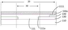
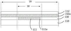
本实施例提供一种有机发光显示面板,该有机发光显示面板例如为柔性显示面板。如图1所示,该有机发光显示面板包括显示区10和周边区20;如图3所示,周边区包括第一走线150a;如图2所示,显示区包括遮光层150和指纹识别电路120,遮光层150包括至少一个开孔151,遮光层150的至少一个开孔151与指纹识别电路120在垂直于面板的表面方向上彼此对应(例如彼此至少部分重叠)且使得穿过开孔151的光可以照射到指纹识别电路120上,用于实现指纹识别。遮光层150与第一走线150a位于同一层。This embodiment provides an organic light emitting display panel, which is, for example, a flexible display panel. As shown in FIG. 1, the organic light emitting display panel includes a
本实施例中,遮光层150与第一走线150a位于同一层是指遮光层150与第一走线150a为同一薄膜或叠层通过例如构图工艺形成得到,因此在该有机发光显示面板的制备过程中,遮光层150与第一走线150a可以在同一构图工艺中形成,无需通过单独构图工艺来形成遮光层150,因此简化了显示面板的制备工艺。例如,遮光层150与第一走线150a的材料可以为钛、铝、钼、铜等金属或者其合金,例如,遮光层150与第一走线150a的材料还可以为钛/铝/钛三层金属或者钼/铝/钼三层金属等多层金属材料,本实施例对此不做限定。In this embodiment, the light-
例如,本实施例中,如图2所示,显示区10还可以包括衬底基板110和设置于衬底基板110上的发光元件203。例如,遮光层150设置于发光元件203的靠近衬底基板110的一侧,即遮光层150比发光元件203更靠近衬底基板110。例如,衬底基板110为柔性基板,其材料例如可以为聚酰亚胺、聚酯(PET)、聚甲基丙烯酸甲酯(PMMA)等,本实施例对此不做限定。例如,发光元件203包括像素电极127、发光层128以及公共电极129。在对像素电极127和公共电极129施加电压时,发光层128例如会发出红、黄或蓝等颜色的光。For example, in this embodiment, as shown in FIG. 2 , the
例如,如图2所示,显示区还可以包括用于驱动发光元件203发光的像素驱动电路,该像素驱动电路包括驱动晶体管、开关晶体管、存储电容等,图中的薄膜晶体管201作为驱动晶体管,将来自电源线的电源电压施加至发光元件203。遮光层150例如可以设置于薄膜晶体管201和发光元件203之间,因此不影响发光元件203的发光,不会降低显示面板的发光强度。例如,薄膜晶体管201包括半导体层121、栅极122、源极123以及漏极124等。例如,薄膜晶体管201与遮光层150通过第一平坦层111相绝缘。例如,遮光层150与像素电极127通过第二平坦层112相绝缘。例如,第一平坦层111和第二平坦层112为聚酰亚胺、树脂等有机绝缘材料。For example, as shown in FIG. 2 , the display area may further include a pixel driving circuit for driving the light-emitting
例如,如图1所示,周边区20还可以包括弯折区30。如图3所示,弯折区30包括至少一个凹槽111a以及填充在凹槽111a中的柔性绝缘材料,第一走线150a延伸经过弯折区30。例如,填充在凹槽111a中的柔性绝缘材料对应于第一平坦层111,二者采用相同的材料,例如在同一工艺中制备。第一平坦层111的材料例如可以为聚酰亚胺、树脂(例如丙烯酸树脂、环氧树脂等)等柔性的绝缘材料。例如,在其他示例中,也可以为并列设置多个凹槽111a,例如两个、三个、四个等等,只要使弯折区能够弯折即可。填充在凹槽111a中的柔性绝缘材料在弯折时起到缓冲作用,减少或防止由于弯曲应力导致的破裂的发生。在图4的示意图中,柔性显示面板绕弯折轴线X弯折,图中的上侧与显示区连接,图中的下侧例如用于邦定,例如可以连接带载封装(TCP)、薄膜封装(COF)等,从而用于与驱动芯片(例如时序驱动器T-Con、数据器、栅极驱动器等)电连接。例如,弯折轴线X平行于显示面板的侧边延伸,凹槽平行弯折轴线X延伸。For example, as shown in FIG. 1 , the
例如,本实施例中,弯折区可以包括绝缘层130。例如绝缘层130包括无机材料层,其材料例如可以为氮化硅、氧化硅等。由于无机材料层具有脆性,不易弯折,因此可以将凹槽111a形成在无机材料层中,然后在凹槽111a中填充柔性绝缘材料,从而形成可以弯折的部分,并且还可以形成基本平坦的表面。本实施例中,第一走线150a例如可以在无机材料层上延伸,以用于实现相应电气功能,例如绑定等。上述柔性绝缘材料与绝缘层130相比脆性较小而柔性更大。For example, in this embodiment, the bending region may include the insulating
本实施例中,显示区10中例如也包括绝缘层130。如图2所示,显示区10中的绝缘层130例如包括阻挡层131、缓冲层132、栅绝缘层133、第一层间绝缘层134以及第二层间绝缘层135。例如,弯折区中的绝缘层130可以包括阻挡层131、缓冲层132、栅绝缘层133、第一层间绝缘层134以及第二层间绝缘层135中的一种或几种。例如,显示区10中的缓冲层132由无机材料形成,因此弯折区30中所包括无机材料层例如可以与显示区10中的缓冲层132在同一构图工艺中形成。In this embodiment, the
例如,如图4所示,弯折区30可以在填充柔性绝缘材料的凹槽111a处以平行于衬底基板110的X为轴进行弯折,从而减小显示区10所在平面中周边区20的面积,有利于显示面板的窄边框设计。For example, as shown in FIG. 4 , the bending
例如,显示区10还可以包括第二走线,并且第二走线从显示区10延伸至周边区20,例如第二走线可以与第一走线150a电连接。本实施例不同的示例中,第二走线例如可以是与薄膜晶体管的源极或漏极电连接的用于传输数据信号的走线,第二走线例如也可以是与薄膜晶体管的栅极电连接的用于传输扫描信号的走线,第二走线例如还可以是与薄膜晶体管的源极或漏极电连接的用于传输电源信号的走线,本实施例对此不作限定。相应地,第二走线例如可以与薄膜晶体管的源极或漏极同层或与薄膜晶体管的栅极同层。For example, the
例如,图2示出了第二走线140与薄膜晶体管201的源极123电连接的情况。例如,周边区20还包括第一平坦层111,第一走线150a通过第一平坦层111中的过孔与第二走线140电连接。For example, FIG. 2 shows a case where the
例如,图5A示出了周边区沿平行于各走线延伸方向的截面示意图。如图5A所示,第二走线140可以从显示区10延伸至周边区20,第二走线140与第一走线150a通过形成在第一平坦层中的过孔1111彼此电连接,从而第二走线140可以向第一走线150a传输电信号。本示例中,如图5A所示,第一走线150a在形成第一平坦层111后形成,由于第一走线150a形成在平坦的第一平坦层111上,因此形成的第一走线150a可以更规则,形成的走线图案更可控,从而在弯折区30弯折时不易出现错位、短路等不良情况。For example, FIG. 5A shows a schematic cross-sectional view of the peripheral region along an extending direction parallel to each trace. As shown in FIG. 5A , the
例如,图5B为本实施例提供的显示面板部分走线连接的一个示意图。如图5B所示,每个像素单元的像素驱动电路包括2T1C驱动电路,即包括两个薄膜晶体管(即驱动晶体管DR TFT和开关晶体管SW TFT)以及存储电容,该示例中第二走线140为数据线,用于连接开关晶体管的源极/漏极以及数据驱动芯片200,以提供显示用的数据信号。位于周边区20中的第一走线150a电连接第二走线140并连接到驱动芯片200,从而第一走线150a可以传输从驱动芯片200处获得的数据信号至第二走线140。本示例中,利用位于周边区的第一走线150a为显示区传输数据信号,但是应当理解,本公开的实施例不限于此。For example, FIG. 5B is a schematic diagram of part wiring connections of the display panel provided in this embodiment. As shown in FIG. 5B , the pixel driving circuit of each pixel unit includes a 2T1C driving circuit, that is, includes two thin film transistors (ie, a driving transistor DR TFT and a switching transistor SW TFT) and a storage capacitor. In this example, the
例如,在本实施例的另一个示例中,图6示出了该示例中周边区沿平行于各走线延伸方向的截面示意图。如图6所示,第二走线140可以在整个周边区20延伸而不与第一走线150a电连接。此时,第一平坦层形成在第二走线140上。For example, in another example of the present embodiment, FIG. 6 shows a schematic cross-sectional view of the peripheral region in the example along the extending direction parallel to each trace. As shown in FIG. 6 , the
例如,在该示例中,第一走线和第二走线可以在周边区中交替设置以传输数据信号。例如,图7A为周边区沿垂直于第一走线150a和第二走线140延伸方向的截面示意图。如图7A所示,第一走线150a和第二走线140在第一平坦层111的不同侧交替设置。For example, in this example, the first wiring and the second wiring may be alternately arranged in the peripheral area to transmit data signals. For example, FIG. 7A is a schematic cross-sectional view of the peripheral region along the extending direction perpendicular to the
例如,该示例中,周边区20也可以包括弯折区30,弯折区包括至少一个凹槽111a,第一平坦层形成在第二走线140上以平坦凹槽111a以及第二走线140,第一走线150a和第二走线140延伸越过弯折区30。For example, in this example, the
例如,该示例中,弯折区30中的绝缘层130包括无机材料层,凹槽111a至少形成在无机材料层中,第二走线140设置无机材料层上,第一平坦层111设置在第二走线140上,第一走线150a设置在第一平坦层111上。For example, in this example, the insulating
例如,图7B为本实施例提供的显示面板部分走线连接的另一示意图。如图7B所示,第一走线150a和第二走线140交替越过弯折区30并连接驱动芯片200,从而第一走线150a和第二走线140可以传输从驱动芯片200处获得的数据信号。本示例中,位于不同层的第一走线150a和第二走线140可以共同为显示区传输电信号。当周边区20的面积一定时,双层走线设计可以使面积一定的周边区20排布更多的走线,或者当显示区的像素过多导致需要在周边区20排布更多的走线时,双层走线还可以缩小用于排布走线的周边区20的面积,有利于显示面板的窄边框设计。另外,第一走线150a和第二走线140在第一平坦层不同侧交替排列还可以使走线排布更加规整,同时位于同层的相邻走线间距较大,从而弯折区30进行弯折时,可以避免各走线出现错位、短路的情况。For example, FIG. 7B is another schematic diagram of part wiring connections of the display panel provided in this embodiment. As shown in FIG. 7B , the
本实施例中,如图2所示,显示面板的子像素例如还包括存储电容202(其包括第一极板125和第二极板126)、像素界定层113、封装层190(包括第一无机材料层191、有机材料层192以及第二无机材料层193组成的三层结构)等其他结构,本实施例对此不做限定。例如存储电容202的两个极板分别与晶体管201的栅极和源极/漏极电连接。In this embodiment, as shown in FIG. 2 , the sub-pixels of the display panel further include, for example, a storage capacitor 202 (which includes a
例如,本实施例中,遮光层和指纹识别电路构成显示区中的指纹识别单元;指纹识别电路与处理器电连接,将采集到的信号发送给处理器以进一步处理得到的指纹图像,以用于解锁、支付等应用。指纹识别电路120为光学指纹识别电路,例如可以包括光电二极管和开关晶体管,光电二极管可以将照射到其上的可见光或红外光信号转换为电信号,开关晶体管可以与光电二极管电连接,以控制光电二极管是否处于采集光信号的状态以及采集光信号的时间。例如,光电二极管的类型和设置方式可以根据实际应用需求进行设定,本公开的实施例对此不做具体限定。例如,光电二极管可以是PIN结型光敏二极管或光敏晶体管等,由此可以提升光电二极管的响应速度。For example, in this embodiment, the light-shielding layer and the fingerprint identification circuit constitute a fingerprint identification unit in the display area; the fingerprint identification circuit is electrically connected to the processor, and the collected signal is sent to the processor to further process the obtained fingerprint image for use in For unlocking, payment and other applications. The
例如,指纹识别单元在工作时,如图8所示,用户的手指按压在显示面板表面,例如按压在封装层190上的手指可以将显示面板中发光元件发出的光反射,从而手指的指纹信息可以通过遮光层150中的开孔151传输到与其相对设置的指纹识别电路120上(基于小孔成像原理),从而指纹识别电路120可以对指纹信息进行采集,所采集的电信号被转化为可进行数字化处理的指纹图像。For example, when the fingerprint identification unit is working, as shown in FIG. 8 , the user's finger presses on the surface of the display panel, for example, the finger pressed on the
例如,本实施例中,如图9所示,遮光层150可以包括多个开孔151。例如,图9中示出了九个开孔151,在其他实施例中,开孔的数量也可以为其它值,例如四个、六个、八个或者十个等等,本实施例对此不做限定。例如,多个开孔151可以呈矩阵式排列。如图9所示,多个开孔151例如可以同时或分时采集指纹数据,由于每个开孔151的尺寸可能比较小,因此一个开孔151所获得的指纹数据可能并不完整,因此可以将对应于多个开孔151的指纹识别电路120获得的多个指纹数据120a进行拼接,从而获得完整的指纹图案。For example, in this embodiment, as shown in FIG. 9 , the
需要说明的是,遮光层150例如还可以包括过孔152,以使像素电极127可以电连接到薄膜晶体管201的漏极,过孔152不影响指纹识别单元的指纹识别功能。It should be noted that the
例如,本实施例中,位于显示区的指纹识别电路可以设置于衬底基板的靠近遮光层一侧的表面或者远离遮光层一侧的表面,本实施例对此不做限定。例如,图2示出了指纹识别电路120设置于衬底基板110的靠近遮光层150一侧表面的情况。需要说明的是,指纹识别电路120也可以设置在衬底基板110上的绝缘层130中的某一位置,例如与阻挡层131同层设置、与缓冲层132同层设置、与第一层间绝缘层134同层设置或者设置于第二层间绝缘层135上等等,只要指纹识别电路120不影响显示区的显示即可,这些情况也属于本公开保护的范围之内。For example, in this embodiment, the fingerprint identification circuit located in the display area may be disposed on the surface of the base substrate on the side close to the light shielding layer or the surface on the side away from the light shielding layer, which is not limited in this embodiment. For example, FIG. 2 shows a case where the
本实施例中,指纹识别单元设置在显示区而不是非显示区中,可以实现屏下指纹识别功能,因此可以缩小周边区的面积,利于显示面板的窄边框设计。另外,指纹识别单元中的遮光层可以与周边区中的第一走线同层设置,因此可以在同一构图工艺中形成,该设计整合了显示区与周边区的制备工艺,简化了工艺流程。In this embodiment, the fingerprint identification unit is arranged in the display area instead of the non-display area, which can realize the fingerprint identification function under the screen, so the area of the peripheral area can be reduced, which is beneficial to the narrow frame design of the display panel. In addition, the light-shielding layer in the fingerprint identification unit can be arranged in the same layer as the first wiring in the peripheral area, so it can be formed in the same patterning process. This design integrates the preparation process of the display area and the peripheral area, which simplifies the process flow.
本公开的至少一个实施例提供了一种显示装置。例如,该显示装置包括本公开任一实施例提供的显示面板。该显示装置可以为手机、平板电脑、电视机、显示器、笔记本电脑、数码相框、导航仪等任何具有显示功能的产品或部件。At least one embodiment of the present disclosure provides a display device. For example, the display device includes the display panel provided by any embodiment of the present disclosure. The display device can be any product or component with a display function, such as a mobile phone, a tablet computer, a TV, a monitor, a notebook computer, a digital photo frame, and a navigator.
需要说明的是,对于本公开的显示面板和显示装置的其它必不可少的组成部分(例如图像数据编码/解码装置、行扫描驱动器、列扫描驱动器、时钟电路等)可以采用适用的常规部件,这些是本领域的普通技术人员所应该理解的,在此不做赘述,也不应作为对本公开实施例的限制。It should be noted that for other essential components of the display panel and display device of the present disclosure (eg, image data encoding/decoding device, row scan driver, column scan driver, clock circuit, etc.), applicable conventional components can be used, These should be understood by those of ordinary skill in the art, and will not be repeated here, nor should they be used as limitations to the embodiments of the present disclosure.
实施例二Embodiment 2
本实施例提供一种有机发光显示面板的制备方法,该方法包括形成显示区和周边区;如图10B所示,在周边区20形成第一走线150a;如图10A所示,在显示区10形成遮光层150和提供指纹识别电路120,遮光层150包括至少一个开孔151,遮光层150与指纹识别电路120在垂直于面板的表面方向上彼此至少部分重叠且使得穿过开孔151的光可以照射到指纹识别电路120上。本实施例中,遮光层150与第一走线150a采用同一薄膜层并通过同一构图工艺形成。This embodiment provides a method for preparing an organic light emitting display panel, the method includes forming a display area and a peripheral area; as shown in FIG. 10B , forming a
例如,遮光层150与第一走线150a的材料可以为钛、铝、钼、铜等金属或者其合金,例如,遮光层150与第一走线150a的材料还可以为钛/铝/钛三层金属或者钼/铝/钼三层金属等多层金属材料,本实施例对此不做限定。For example, the material of the
例如,一次构图工艺可以包括光刻胶的涂覆、曝光、显影、刻蚀等工序,本实施例不再赘述。For example, one patterning process may include photoresist coating, exposure, development, etching and other processes, which will not be repeated in this embodiment.
本实施例中,指纹识别单元形成在显示区而不是非显示区中,因此可以缩小周边区的面积,利于显示面板的窄边框设计。另外,指纹识别单元中的遮光层与周边区中的第一走线在同一构图工艺中形成,整合了显示区与周边区的制备工艺,简化了工艺流程。In this embodiment, the fingerprint identification unit is formed in the display area instead of the non-display area, so the area of the peripheral area can be reduced, which is beneficial to the narrow frame design of the display panel. In addition, the light-shielding layer in the fingerprint identification unit and the first wiring in the peripheral area are formed in the same patterning process, which integrates the preparation process of the display area and the peripheral area, and simplifies the process flow.
例如,本实施例提供的有机发光显示面板的制备方法还可以包括形成薄膜晶体管201、电容202、绝缘层130等步骤,这些结构的基本构成可以参见上述实施例,并且这些结构可以采用构图工艺等方法形成,本实施例不再赘述。For example, the method for preparing an organic light-emitting display panel provided in this embodiment may further include steps such as forming a
例如,如图10A所示,遮光层150可以形成于薄膜晶体管201的上方。例如,在薄膜晶体管201上形成第一平坦层111,然后在第一平坦层111上形成遮光层150。For example, as shown in FIG. 10A , the
例如,本实施例提供的有机发光显示面板的制备方法还可以包括:在遮光层中形成呈矩阵式排列的多个开孔。例如,多个开孔例如可以形成在图10A中开孔151附近的位置,只要不影响显示区的显示效果以及指纹识别单元的指纹识别功能即可。For example, the method for fabricating an organic light emitting display panel provided in this embodiment may further include: forming a plurality of openings arranged in a matrix in the light shielding layer. For example, a plurality of openings may be formed at positions near the
例如,本实施例中,如图10A所示,在遮光层150中形成开孔151的同时还可以形成过孔152,以用于之后形成像素电极等结构。For example, in this embodiment, as shown in FIG. 10A , while forming the
例如,本实施例中,形成于显示区的指纹识别电路可以形成在衬底基板的靠近遮光层一侧的表面或者远离遮光层一侧的表面,本实施例对此不做限定。For example, in this embodiment, the fingerprint identification circuit formed in the display area may be formed on the surface of the base substrate on the side close to the light shielding layer or the surface on the side away from the light shielding layer, which is not limited in this embodiment.
例如,图10A示出了指纹识别电路120形成于衬底基板110的靠近遮光层150一侧表面的情况。需要说明的是,指纹识别电路120也可以形成在衬底基板110上的绝缘层130中的某一位置,例如与阻挡层131同层形成、与缓冲层132同层形成、与第一层间绝缘层134同层形成或者形成于第二层间绝缘层135上等等,只要指纹识别电路120不影响显示区的显示即可,这些情况也属于本公开保护的范围之内。For example, FIG. 10A shows a case where the
例如,在本实施例提供的有机发光显示面板的制备方法中,如图10B所示,可以在周边区形成至少一个凹槽111a并在凹槽111a中填充柔性绝缘材料以形成弯折区。例如,第一走线150a可以延伸越过弯折区。例如,在其他示例中,凹槽111a也可以形成为并列设置的多个,例如两个、三个、四个等等,只要使弯折区能够弯折即可。For example, in the method for fabricating an organic light emitting display panel provided in this embodiment, as shown in FIG. 10B , at least one
例如,填充在凹槽111a中的柔性绝缘材料为第一平坦层111,第一平坦层111的材料例如可以为聚酰亚胺、树脂等柔性的绝缘材料。For example, the flexible insulating material filled in the
例如,弯折区中的绝缘层130包括无机材料层,其材料例如可以为氮化硅、氧化硅等。由于无机材料层具有脆性,不易弯折,因此可以将凹槽111a形成在无机材料层中,然后在凹槽111a中填充柔性绝缘材料,从而形成可以弯折的部分。本实施例中,第一走线150a例如可以形成为在无机材料层上延伸。For example, the insulating
本实施例中,显示区10中也形成绝缘层130。例如,显示区10中形成的绝缘层130包括阻挡层131、缓冲层132、栅绝缘层133、第一层间绝缘层134以及第二层间绝缘层135。例如,弯折区中形成的绝缘层130可以包括阻挡层131、缓冲层132、栅绝缘层133、第一层间绝缘层134以及第二层间绝缘层135中的一种或几种。例如,显示区10中的缓冲层132由无机材料形成,因此至少弯折区30中所包括的无机材料层可以与显示区10中的缓冲层132在同一构图工艺中形成。In this embodiment, the insulating
例如,弯折区可以在填充柔性绝缘材料的凹槽111a处进行弯折,从而减小显示区所在平面中周边区的面积,有利于显示面板的窄边框设计。For example, the bending area can be bent at the
例如,如图10A所示,还可以在显示区中形成第二走线140,第二走线140从显示区延伸至周边区,在周边区中,第一走线150a形成为与第二走线电连接。For example, as shown in FIG. 10A , the
例如,参见图5A,在周边区20形成第一平坦层111,然后在平坦层111中形成暴露第二走线140的过孔1111,之后形成第一走线150a,从而第一走线150a可以通过第一平坦层111中的过孔与第二走线140电连接。本示例中,第一走线150a在形成第一平坦层111之后形成,由于第一走线150a形成在平坦的第一平坦层111上,因此形成的第一走线150a可以更规整,形成的走线图案更可控,在弯折区30弯折时不易出现错位、短路等不良情况。For example, referring to FIG. 5A , a first
例如,在另一个示例中,参见图6,第二走线140可以形成为在整个周边区20延伸,而不与第一走线150a电连接。此时,第一平坦层形成在第二走线140上。For example, in another example, referring to FIG. 6 , the
例如,在该示例中,第一走线150a和第二走线140可以在周边区20中交替形成以传输数据信号。例如,参见图7A,第一走线150a和第二走线140在第一平坦层111的不同侧交替形成。例如,首先形成第二走线140,然后在第二走线140上形成第一平坦层111,之后在第一平坦层111上的对应于第二走线140间隔的位置形成第一走线150a,此时,第一走线150a与第二走线140的连接结构与图5A中所示的结构基本相同,因此不再赘述。在第一走线150a形成后,还可以形成第二平坦层112。For example, in this example, the
例如,该示例中,周边区20中也可以形成弯折区30,该弯折区中形成至少一个凹槽111a,第一平坦层形成在第二走线140上以平坦凹槽111a以及第二走线140,第一走线150a和第二走线140延伸越过弯折区30。For example, in this example, a bending
例如,该示例中,弯折区30中形成的绝缘层130包括无机材料层,凹槽111a至少形成在无机材料层中,第二走线140设置无机材料层上,第一平坦层111设置在第二走线140上,第一走线150a设置在第一平坦层111上。For example, in this example, the insulating
本示例中,形成于不同层的第一走线150a和第二走线140可以共同为显示区传输数据信号。当周边区20的面积一定时,双层走线设计可以使面积一定的周边区20排布更多的走线,或者当显示区的像素过多导致需要在周边区20排布更多的走线时,双层走线还可以缩小用于排布走线的周边区20的面积,有利于显示面板的窄边框设计。另外,第一走线150a和第二走线140在第一平坦层不同侧交替形成还可以使走线排布更加规整,同时位于同层的相邻走线间距较大,从而弯折区30进行弯折时,可以避免各走线出现错位、短路的情况。In this example, the
需要说明的是,本实施例中,形成显示区还可以包括形成像素界定层、有机发光元件、封装元件等结构,这些结构可以采用常规方法形成,本实施例对此不做限定。It should be noted that, in this embodiment, forming the display area may also include forming structures such as pixel defining layers, organic light-emitting elements, packaging elements, etc. These structures may be formed by conventional methods, which are not limited in this embodiment.
还有以下几点需要说明:There are a few more points to note:
(1)本公开实施例附图只涉及到与本公开实施例涉及到的结构,其他结构可参考通常设计。(1) The accompanying drawings of the embodiments of the present disclosure only relate to the structures involved in the embodiments of the present disclosure, and other structures may refer to general designs.
(2)为了清晰起见,在用于描述本公开的实施例的附图中,层或区域的厚度被放大或缩小,即这些附图并非按照实际的比例绘制。可以理解,当诸如层、膜、区域或基板之类的元件被称作位于另一元件“上”或“下”时,该元件可以“直接”位于另一元件“上”或“下”或者可以存在中间元件。(2) In the drawings for describing the embodiments of the present disclosure, the thicknesses of layers or regions are exaggerated or reduced for clarity, ie, the drawings are not drawn on actual scale. It will be understood that when an element such as a layer, film, region or substrate is referred to as being "on" or "under" another element, it can be "directly on" or "under" the other element, or Intermediate elements may be present.
(3)在不冲突的情况下,本公开的实施例及实施例中的特征可以相互组合以得到新的实施例。(3) The embodiments of the present disclosure and the features in the embodiments may be combined with each other to obtain new embodiments without conflict.
以上所述,仅为本公开的具体实施方式,但本公开的保护范围并不局限于此,任何熟悉本技术领域的技术人员在本公开揭露的技术范围内,可轻易想到变化或替换,都应涵盖在本公开的保护范围之内。因此,本公开的保护范围应以权利要求的保护范围为准。The above are only specific embodiments of the present disclosure, but the protection scope of the present disclosure is not limited to this. should be included within the scope of protection of the present disclosure. Therefore, the protection scope of the present disclosure should be subject to the protection scope of the claims.
Claims (15)
Priority Applications (2)
| Application Number | Priority Date | Filing Date | Title |
|---|---|---|---|
| CN201810032053.XACN108242462B (en) | 2018-01-12 | 2018-01-12 | Organic light-emitting display panel, preparation method thereof, and display device |
| US16/149,330US11036958B2 (en) | 2018-01-12 | 2018-10-02 | Light emitting display panel and manufacture method thereof, display device |
Applications Claiming Priority (1)
| Application Number | Priority Date | Filing Date | Title |
|---|---|---|---|
| CN201810032053.XACN108242462B (en) | 2018-01-12 | 2018-01-12 | Organic light-emitting display panel, preparation method thereof, and display device |
Publications (2)
| Publication Number | Publication Date |
|---|---|
| CN108242462A CN108242462A (en) | 2018-07-03 |
| CN108242462Btrue CN108242462B (en) | 2020-08-18 |
Family
ID=62699551
Family Applications (1)
| Application Number | Title | Priority Date | Filing Date |
|---|---|---|---|
| CN201810032053.XAActiveCN108242462B (en) | 2018-01-12 | 2018-01-12 | Organic light-emitting display panel, preparation method thereof, and display device |
Country Status (2)
| Country | Link |
|---|---|
| US (1) | US11036958B2 (en) |
| CN (1) | CN108242462B (en) |
Families Citing this family (39)
| Publication number | Priority date | Publication date | Assignee | Title |
|---|---|---|---|---|
| KR102562900B1 (en)* | 2018-02-02 | 2023-08-04 | 삼성디스플레이 주식회사 | Flexible display apparatus and touch sensitive display apparatus |
| CN108735101B (en)* | 2018-05-28 | 2020-01-31 | 京东方科技集团股份有限公司 | flexible display device |
| CN109101903B (en) | 2018-07-25 | 2020-12-04 | 京东方科技集团股份有限公司 | A display panel and display device |
| CN109036134B (en)* | 2018-08-01 | 2021-01-26 | 京东方科技集团股份有限公司 | Flexible display substrate, manufacturing method thereof, and display device |
| CN109065590B (en)* | 2018-08-09 | 2020-12-04 | 京东方科技集团股份有限公司 | Organic light-emitting display substrate and method of making the same, and organic light-emitting display device |
| CN109148529B (en) | 2018-08-20 | 2021-11-02 | 武汉华星光电半导体显示技术有限公司 | Substrate and display device |
| CN109273497B (en) | 2018-09-21 | 2021-01-12 | 京东方科技集团股份有限公司 | OLED display substrate and display device |
| CN109273498B (en)* | 2018-09-25 | 2021-01-26 | 京东方科技集团股份有限公司 | Array substrate, preparation method thereof, display panel and display device |
| CN208766968U (en) | 2018-09-29 | 2019-04-19 | 昆山国显光电有限公司 | A flexible display panel and flexible display device |
| KR102654289B1 (en)* | 2018-10-05 | 2024-04-03 | 삼성디스플레이 주식회사 | Display device and manufacturing method thereof |
| CN109451106B (en)* | 2018-11-16 | 2020-06-12 | Oppo广东移动通信有限公司 | Electronic device |
| CN109493728B (en)* | 2018-12-13 | 2022-10-14 | 云谷(固安)科技有限公司 | Display panel and display device |
| CN109545837B (en)* | 2018-12-17 | 2020-10-13 | 武汉华星光电半导体显示技术有限公司 | AMOLED flexible display device |
| CN109686770B (en) | 2018-12-25 | 2021-04-16 | 上海天马微电子有限公司 | Display panels and display devices |
| CN109753933A (en)* | 2019-01-09 | 2019-05-14 | 昆山国显光电有限公司 | Fingerprint recognition panel |
| CN109755285B (en)* | 2019-02-01 | 2022-12-06 | 合肥鑫晟光电科技有限公司 | Display panel, manufacturing method thereof and display device |
| CN109887963B (en)* | 2019-02-18 | 2021-07-06 | 武汉华星光电半导体显示技术有限公司 | An OLED display panel |
| CN109712527B (en)* | 2019-03-06 | 2022-11-15 | 广州国显科技有限公司 | Display device for identifying fingerprints under screen |
| CN109785756B (en)* | 2019-03-15 | 2022-07-05 | 昆山国显光电有限公司 | Display panel and display device |
| CN109993141B (en)* | 2019-04-10 | 2021-09-03 | 京东方科技集团股份有限公司 | OLED display panel, fingerprint identification method and display device |
| CN109887985B (en)* | 2019-04-10 | 2022-08-16 | 京东方科技集团股份有限公司 | Array substrate, display panel and display device |
| CN110112193B (en)* | 2019-04-29 | 2021-10-15 | 上海天马微电子有限公司 | Organic light-emitting display panel and organic light-emitting display device |
| KR20210013500A (en)* | 2019-07-26 | 2021-02-04 | 삼성디스플레이 주식회사 | Display device |
| CN110866506B (en)* | 2019-11-20 | 2022-03-15 | 厦门天马微电子有限公司 | Display panel and display device |
| CN110943100A (en)* | 2019-12-02 | 2020-03-31 | 多感科技(上海)有限公司 | Ultra-thin imaging chip and method for forming the same, imaging module and method for forming the same |
| US20230006010A1 (en)* | 2019-12-17 | 2023-01-05 | Sharp Kabushiki Kaisha | Display device |
| KR102778739B1 (en)* | 2020-01-17 | 2025-03-12 | 삼성디스플레이 주식회사 | Display device and portable terminal |
| CN111968520B (en)* | 2020-09-04 | 2024-03-26 | 京东方科技集团股份有限公司 | Display module, manufacturing method of display module, display panel and display device |
| US11844250B2 (en)* | 2020-09-17 | 2023-12-12 | Chengdu Boe Optoelectronics Technology Co., Ltd. | Display panel including grooved inorganic layer in bending area and display device including display panel |
| CN112259582B (en)* | 2020-10-15 | 2023-01-24 | 武汉华星光电半导体显示技术有限公司 | Flexible display panel and electronic device |
| CN113066840B (en)* | 2021-03-22 | 2024-05-24 | 京东方科技集团股份有限公司 | Display panel and manufacturing method thereof, and display device |
| CN113097268B (en)* | 2021-03-30 | 2024-04-12 | 上海天马微电子有限公司 | Display panel and electronic equipment |
| CN113257836B (en)* | 2021-05-07 | 2022-08-05 | 武汉华星光电半导体显示技术有限公司 | Array substrate and display panel |
| CN114550227B (en)* | 2021-07-23 | 2024-05-17 | 友达光电股份有限公司 | Optical sensing device |
| WO2023050163A1 (en)* | 2021-09-29 | 2023-04-06 | 京东方科技集团股份有限公司 | Fingerprint recognition substrate, electronic device and fingerprint recognition method |
| CN116209302A (en) | 2021-11-29 | 2023-06-02 | 荣耀终端有限公司 | Display panel, manufacturing method thereof and terminal equipment |
| CN114678334B (en)* | 2022-03-25 | 2025-09-05 | 京东方科技集团股份有限公司 | Narrow-frame display panel and display device |
| WO2024150419A1 (en)* | 2023-01-13 | 2024-07-18 | シャープディスプレイテクノロジー株式会社 | Display device and method for manufacturing same |
| WO2024166389A1 (en)* | 2023-02-10 | 2024-08-15 | シャープディスプレイテクノロジー株式会社 | Display device |
Citations (6)
| Publication number | Priority date | Publication date | Assignee | Title |
|---|---|---|---|---|
| CN104881170A (en)* | 2015-05-08 | 2015-09-02 | 厦门天马微电子有限公司 | Array substrate, display panel, display apparatus and manufacturing method |
| CN106096595A (en)* | 2016-08-08 | 2016-11-09 | 京东方科技集团股份有限公司 | A kind of fingerprint recognition module, its manufacture method and fingerprint recognition display device |
| CN106601133A (en)* | 2017-02-28 | 2017-04-26 | 京东方科技集团股份有限公司 | Flexible display panel, making method thereof and display device |
| CN106716642A (en)* | 2014-09-30 | 2017-05-24 | 乐金显示有限公司 | Display device with separate wiring patterns |
| CN106940488A (en)* | 2017-04-27 | 2017-07-11 | 上海天马微电子有限公司 | Display panel and display device |
| CN107086236A (en)* | 2016-02-12 | 2017-08-22 | 三星显示有限公司 | display device |
Family Cites Families (9)
| Publication number | Priority date | Publication date | Assignee | Title |
|---|---|---|---|---|
| KR100448448B1 (en)* | 2001-07-12 | 2004-09-13 | 주식회사 디알텍 | Switching element of X-ray panel and the same method |
| CN103942537A (en) | 2014-04-04 | 2014-07-23 | 王曙光 | Liquid crystal terminal device, fingerprint image collection method and fingerprint collector |
| CN203838722U (en) | 2014-04-04 | 2014-09-17 | 深圳印象认知技术有限公司 | Liquid crystal terminal equipment and fingerprint acquisition device |
| KR102463838B1 (en) | 2015-08-24 | 2022-11-04 | 삼성디스플레이 주식회사 | Flexible display device and manufacturing method thereof |
| US10430000B2 (en)* | 2016-08-05 | 2019-10-01 | Innolux Corporation | Touch display device |
| US10741621B2 (en)* | 2016-11-25 | 2020-08-11 | Lg Display Co., Ltd. | Display device with a fingerprint sensor |
| CN110825171B (en)* | 2017-04-27 | 2023-06-20 | Oppo广东移动通信有限公司 | Display screen, display device and mobile terminal |
| KR102410542B1 (en)* | 2017-05-29 | 2022-06-20 | 삼성전자주식회사 | Electronic device comprising a module mounted on sunken area of layer |
| KR20190006374A (en)* | 2017-07-10 | 2019-01-18 | 삼성전자주식회사 | The Image Sensor including the Blocking Member for blocking the interference between a plurality of light receiving sensors and the Electronic Device including the Image Sensor |
- 2018
- 2018-01-12CNCN201810032053.XApatent/CN108242462B/enactiveActive
- 2018-10-02USUS16/149,330patent/US11036958B2/enactiveActive
Patent Citations (6)
| Publication number | Priority date | Publication date | Assignee | Title |
|---|---|---|---|---|
| CN106716642A (en)* | 2014-09-30 | 2017-05-24 | 乐金显示有限公司 | Display device with separate wiring patterns |
| CN104881170A (en)* | 2015-05-08 | 2015-09-02 | 厦门天马微电子有限公司 | Array substrate, display panel, display apparatus and manufacturing method |
| CN107086236A (en)* | 2016-02-12 | 2017-08-22 | 三星显示有限公司 | display device |
| CN106096595A (en)* | 2016-08-08 | 2016-11-09 | 京东方科技集团股份有限公司 | A kind of fingerprint recognition module, its manufacture method and fingerprint recognition display device |
| CN106601133A (en)* | 2017-02-28 | 2017-04-26 | 京东方科技集团股份有限公司 | Flexible display panel, making method thereof and display device |
| CN106940488A (en)* | 2017-04-27 | 2017-07-11 | 上海天马微电子有限公司 | Display panel and display device |
Also Published As
| Publication number | Publication date |
|---|---|
| CN108242462A (en) | 2018-07-03 |
| US20190220644A1 (en) | 2019-07-18 |
| US11036958B2 (en) | 2021-06-15 |
Similar Documents
| Publication | Publication Date | Title |
|---|---|---|
| CN108242462B (en) | Organic light-emitting display panel, preparation method thereof, and display device | |
| US11054686B2 (en) | Display panel including OLEDS and micro-LEDS, the manufacturing method of the display panel, and display device utilizing the display panel and achieving a narrow border region | |
| US11342390B2 (en) | Display panel, display device and a method for manufacturing a display panel | |
| US11424298B2 (en) | Display panel and display device | |
| CN109859648B (en) | Display panel and display device | |
| KR101908501B1 (en) | Integrated Touch Screen With Organic Emitting Display Device and Method for Manufacturing the Same | |
| KR102683935B1 (en) | Display device with integrated touch screen and method for fabricating the same | |
| KR102387631B1 (en) | Display device with integrated touch screen and method for fabricating the same | |
| CN108735786B (en) | Organic light-emitting display panel and organic light-emitting display device | |
| CN114582949A (en) | Display substrate and display device | |
| KR102864248B1 (en) | Display device | |
| WO2021244251A1 (en) | Display substrate and display device | |
| WO2018028303A1 (en) | Fingerprint recognition module and manufacturing method therefor and display device | |
| CN114792707A (en) | Display substrate and display device | |
| KR102262683B1 (en) | Touch display device | |
| CN113451375A (en) | Display panel, method of manufacturing the same, and display device having the same | |
| TWI815445B (en) | Flexible display apparatus | |
| CN108279810A (en) | Display module and preparation method thereof, display device | |
| KR20230151587A (en) | Display device | |
| CN115249729A (en) | Display panel, electronic device including the same, and method of manufacturing the electronic device | |
| CN114840098A (en) | Touch display panel and manufacturing method thereof, touch display screen and spliced screen | |
| CN218101267U (en) | display device | |
| CN116390596A (en) | Display panel and display device | |
| CN111293159B (en) | Display substrate and display device | |
| CN112736115B (en) | Method for manufacturing circuit board and display device including circuit board |
Legal Events
| Date | Code | Title | Description |
|---|---|---|---|
| PB01 | Publication | ||
| PB01 | Publication | ||
| SE01 | Entry into force of request for substantive examination | ||
| SE01 | Entry into force of request for substantive examination | ||
| GR01 | Patent grant | ||
| GR01 | Patent grant |