CN108190832B - OLED panel and manufacturing method thereof - Google Patents
OLED panel and manufacturing method thereofDownload PDFInfo
- Publication number
- CN108190832B CN108190832BCN201711479105.XACN201711479105ACN108190832BCN 108190832 BCN108190832 BCN 108190832BCN 201711479105 ACN201711479105 ACN 201711479105ACN 108190832 BCN108190832 BCN 108190832B
- Authority
- CN
- China
- Prior art keywords
- packaging material
- layer
- substrate
- composite packaging
- cover plate
- Prior art date
- Legal status (The legal status is an assumption and is not a legal conclusion. Google has not performed a legal analysis and makes no representation as to the accuracy of the status listed.)
- Active
Links
Images


Classifications
- H—ELECTRICITY
- H10—SEMICONDUCTOR DEVICES; ELECTRIC SOLID-STATE DEVICES NOT OTHERWISE PROVIDED FOR
- H10K—ORGANIC ELECTRIC SOLID-STATE DEVICES
- H10K71/00—Manufacture or treatment specially adapted for the organic devices covered by this subclass
- B—PERFORMING OPERATIONS; TRANSPORTING
- B82—NANOTECHNOLOGY
- B82Y—SPECIFIC USES OR APPLICATIONS OF NANOSTRUCTURES; MEASUREMENT OR ANALYSIS OF NANOSTRUCTURES; MANUFACTURE OR TREATMENT OF NANOSTRUCTURES
- B82Y30/00—Nanotechnology for materials or surface science, e.g. nanocomposites
- H—ELECTRICITY
- H10—SEMICONDUCTOR DEVICES; ELECTRIC SOLID-STATE DEVICES NOT OTHERWISE PROVIDED FOR
- H10K—ORGANIC ELECTRIC SOLID-STATE DEVICES
- H10K59/00—Integrated devices, or assemblies of multiple devices, comprising at least one organic light-emitting element covered by group H10K50/00
- H10K59/80—Constructional details
- H10K59/87—Passivation; Containers; Encapsulations
- H10K59/871—Self-supporting sealing arrangements
- H10K59/8722—Peripheral sealing arrangements, e.g. adhesives, sealants
- H—ELECTRICITY
- H10—SEMICONDUCTOR DEVICES; ELECTRIC SOLID-STATE DEVICES NOT OTHERWISE PROVIDED FOR
- H10K—ORGANIC ELECTRIC SOLID-STATE DEVICES
- H10K59/00—Integrated devices, or assemblies of multiple devices, comprising at least one organic light-emitting element covered by group H10K50/00
- H10K59/80—Constructional details
- H10K59/87—Passivation; Containers; Encapsulations
- H10K59/874—Passivation; Containers; Encapsulations including getter material or desiccant
Landscapes
- Engineering & Computer Science (AREA)
- Chemical & Material Sciences (AREA)
- Nanotechnology (AREA)
- Manufacturing & Machinery (AREA)
- Physics & Mathematics (AREA)
- Composite Materials (AREA)
- Condensed Matter Physics & Semiconductors (AREA)
- General Physics & Mathematics (AREA)
- Materials Engineering (AREA)
- Crystallography & Structural Chemistry (AREA)
- Electroluminescent Light Sources (AREA)
Abstract
Translated fromChinese
Description
Translated fromChinese技术领域technical field
本发明涉及半导体封装技术领域,尤其涉及一种OLED面板及其制作方法。The present invention relates to the technical field of semiconductor packaging, and in particular, to an OLED panel and a manufacturing method thereof.
背景技术Background technique
OLED即有机发光二极管(Organic Light-Emitting Diode),具备自发光、高亮度、宽视角、高对比度、可挠曲、低能耗等特性,因此受到广泛的关注,并作为新一代的显示方式,已开始逐渐取代传统液晶显示器,被广泛应用在手机屏幕、电脑显示器、全彩电视等。OLED显示技术与传统的LCD显示方式不同,无需背光灯,采用非常薄的有机材料涂层和玻璃基板,当有电流通过时,这些有机材料就会发光。但是由于有机材料易与水氧反应,作为基于有机材料的显示设备,OLED显示屏对封装的要求非常高。为了实现OLED显示面板商业化,与之相关的封装技术成为了研究热点。OLED is an organic light-emitting diode (Organic Light-Emitting Diode), which has the characteristics of self-luminescence, high brightness, wide viewing angle, high contrast, flexibility, and low energy consumption. It began to gradually replace traditional liquid crystal displays, and was widely used in mobile phone screens, computer monitors, full-color TVs, etc. Unlike traditional LCD displays, OLED display technology does not require a backlight and uses a very thin coating of organic materials and glass substrates that emit light when an electric current flows through them. However, since organic materials easily react with water and oxygen, as a display device based on organic materials, OLED displays have very high requirements for packaging. In order to realize the commercialization of OLED display panels, the related packaging technology has become a research hotspot.
由于构成OLED器件的活泼电极和有机发光材料对水汽和氧气非常敏感,水汽和氧气的侵入可以快速恶化OLED的显示效果和寿命。又由于大尺寸OLED器件的寿命要求更高,其封装中常会用到Dam(框胶)和Getter(吸湿剂),由于Dam和Getter宽度较大,造成封装边框较大,对产品的感观产生较大影响,因此有必要开发新的封装技术和材料来实现大尺寸OLED器件的窄边框封装。Since the active electrodes and organic light-emitting materials constituting OLED devices are very sensitive to water vapor and oxygen, the intrusion of water vapor and oxygen can rapidly deteriorate the display effect and lifetime of OLEDs. In addition, due to the higher life expectancy of large-sized OLED devices, Dam (sealant) and Getter (moisture absorbent) are often used in their packaging. Due to the large width of Dam and Getter, the packaging frame is large, which has a negative impact on the appearance of the product. Therefore, it is necessary to develop new packaging technologies and materials to realize the narrow border packaging of large-scale OLED devices.
发明内容SUMMARY OF THE INVENTION
鉴于现有技术存在的不足,本发明提供了一种OLED面板及其制作方法,用纳米瓷光固化树脂取代框胶和吸湿剂,既可以保证封装性能,又能实现窄边框封装。In view of the deficiencies in the prior art, the present invention provides an OLED panel and a manufacturing method thereof. Nano-ceramic photocurable resin is used to replace the sealant and hygroscopic agent, which can not only ensure the encapsulation performance, but also realize the narrow-frame encapsulation.
为了实现上述的目的,本发明采用了如下的技术方案:In order to achieve the above-mentioned purpose, the present invention adopts the following technical scheme:
一种OLED面板,包括基板、盖板、设于所述基板与所述盖板之间的有机发光层、将所述有机发光层封装于所述基板表面的阻水层以及设于所述基板与所述盖板之间的环形的复合封装材料层,所述复合封装材料层绕所述阻水层设置,并将所述有机发光层、所述阻水层密封于所述基板和所述盖板之间,所述复合封装材料层为纳米树脂材料。An OLED panel, comprising a substrate, a cover plate, an organic light-emitting layer disposed between the substrate and the cover plate, a water blocking layer encapsulating the organic light-emitting layer on the surface of the substrate, and an organic light-emitting layer disposed on the substrate an annular composite packaging material layer between the cover plate and the cover plate, the composite packaging material layer is arranged around the water blocking layer, and the organic light-emitting layer and the water blocking layer are sealed on the substrate and the water blocking layer. Between the cover plates, the composite packaging material layer is a nano resin material.
作为其中一种实施方式,所述复合封装材料层为纳米瓷光固化树脂。As one of the embodiments, the composite packaging material layer is a nano-ceramic photocurable resin.
作为其中一种实施方式,所述的OLED面板还包括填充胶,所述填充胶填充于所述阻水层与所述盖板之间,并与所述复合封装材料层贴合。As one of the embodiments, the OLED panel further includes a filler, the filler is filled between the water blocking layer and the cover plate, and is attached to the composite packaging material layer.
作为其中一种实施方式,所述阻水层侧壁与所述复合封装材料层贴合。As one of the embodiments, the sidewall of the water blocking layer is adhered to the composite packaging material layer.
本发明的另一目的在于提供一种OLED面板的制作方法,包括:Another object of the present invention is to provide a method for manufacturing an OLED panel, including:
提供基板和盖板;Provide base plate and cover plate;
在所述盖板上表面制作一圈复合封装材料层,所述复合封装材料层为纳米树脂材料;A circle of composite packaging material layers is made on the upper surface of the cover plate, and the composite packaging material layers are nano-resin materials;
在所述基板上表面制作有机发光层;making an organic light-emitting layer on the upper surface of the substrate;
在所述有机发光层表面制作至少一层阻水层,将所述有机发光层封装于所述基板上;At least one water blocking layer is fabricated on the surface of the organic light-emitting layer, and the organic light-emitting layer is encapsulated on the substrate;
将所述基板与所述盖板真空贴合,并使所述复合封装材料层固化。The substrate and the cover plate are vacuum bonded, and the composite packaging material layer is cured.
作为其中一种实施方式,所述的OLED面板的制作方法还包括:在所述盖板上表面制作一圈复合封装材料层后,在盖板上表面涂布一层填充胶,并使所述填充胶位于所述复合封装材料层围成的区域内。As one of the embodiments, the manufacturing method of the OLED panel further includes: after forming a circle of composite packaging material layers on the surface of the cover plate, coating a layer of filler on the surface of the cover plate, and making the cover plate The filling glue is located in the area enclosed by the composite packaging material layer.
作为其中一种实施方式,所述阻水层为SiNx、SiON、SiOx、Al2O3材料。As one of the embodiments, the water blocking layer is made of SiNx, SiON, SiOx, and Al2 O3 materials.
作为其中一种实施方式,所述复合封装材料层为纳米瓷光固化树脂。As one of the embodiments, the composite packaging material layer is a nano-ceramic photocurable resin.
作为其中一种实施方式,所述复合封装材料层包括二氧化锆或二氧化硅无机纳米颗粒以及树脂基质,所述无机纳米颗粒均匀分散在所述树脂基质内。As one of the embodiments, the composite encapsulating material layer includes zirconium dioxide or silicon dioxide inorganic nanoparticles and a resin matrix, and the inorganic nanoparticles are uniformly dispersed in the resin matrix.
本发明利用具有较好的粘接力和韧性的纳米树脂材料作为OLED面板的封装材料,可以兼顾致密性和阻水、阻氧性能,从而以此来取代框胶和吸湿剂,实现了大尺寸OLED器件的窄边框封装。The present invention uses nano-resin material with good adhesion and toughness as the packaging material of the OLED panel, which can take into account the compactness, water resistance and oxygen resistance, so as to replace the sealant and the moisture absorbing agent, and realize the large size Narrow bezel encapsulation of OLED devices.
附图说明Description of drawings
图1为本发明实施例的一种OLED面板的结构示意图;FIG. 1 is a schematic structural diagram of an OLED panel according to an embodiment of the present invention;
图2为本发明实施例的另一种OLED面板的结构示意图;FIG. 2 is a schematic structural diagram of another OLED panel according to an embodiment of the present invention;
图3为本发明实施例的一种OLED面板的制作方法流程图;3 is a flowchart of a method for manufacturing an OLED panel according to an embodiment of the present invention;
图4为本发明实施例的一种OLED面板的制作过程示意图。FIG. 4 is a schematic diagram of a manufacturing process of an OLED panel according to an embodiment of the present invention.
具体实施方式Detailed ways
为了使本发明的目的、技术方案及优点更加清楚明白,以下结合附图及实施例,对本发明进一步详细说明。应当理解,此处所描述的具体实施例仅仅用以解释本发明,并不用于限定本发明。In order to make the objectives, technical solutions and advantages of the present invention clearer, the present invention will be further described in detail below with reference to the accompanying drawings and embodiments. It should be understood that the specific embodiments described herein are only used to explain the present invention, but not to limit the present invention.
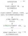
参阅图1,本发明实施例的OLED面板主要包括基板10、盖板20、设于基板10与盖板20之间的有机发光层30、将有机发光层30封装于基板10表面的阻水层40以及设于基板10与盖板20之间的环形的复合封装材料层50,复合封装材料层50绕阻水层40设置,并将有机发光层30、阻水层40密封于基板10和盖板20之间,该复合封装材料层50为纳米树脂材料。Referring to FIG. 1 , the OLED panel according to the embodiment of the present invention mainly includes a
这里,该复合封装材料层50优选为纳米瓷光固化树脂,主要由粒径20-400nm的二氧化锆或二氧化硅无机等纳米颗粒填料以及树脂基质组成,无机纳米颗粒均匀分散在树脂基质内,其能在紫外光照射下快速固化,粘接力强、硬度高、并且具有一定韧性。相比现有技术中的框胶,由于框胶内部只填充了少量10um左右的玻璃珠、硅球或塑料颗粒,其主要成分树脂基质无法起到较好的阻水效果,而纳米瓷光固化树脂中填充了较多的无机纳米颗粒并且均匀分散在树脂基质中,既保证了粘接力和韧性,又具有类似陶瓷的致密性和阻水、阻氧性能,因此,将其作为OLED封装材料省去了框胶和吸湿剂,有利于实现窄边框显示设计。Here, the composite
另外,本实施例的OLED面板内还具有填充胶60,该填充胶60是透明光学胶,经固化后很好地将各组成粘接在一起,该填充胶60填充于阻水层40与盖板20之间,并与复合封装材料层50贴合,且阻水层40侧壁与复合封装材料层50贴合。In addition, the OLED panel of this embodiment also has a
如图2,作为其中一种改进的实施方式,还可以在基板10的表面开设有位于阻水层40外围的凹槽100,复合封装材料层50填充在凹槽100内,该凹槽100的一个侧壁最好与阻水层40侧壁平齐,使得基板10与阻水层40的接触面之间形成阶梯状过渡,外围的复合封装材料层50可以具有更好的封装效果。As shown in FIG. 2 , as an improved embodiment, a
如图3和图4所示,本发明还提供了一种OLED面板的制作方法,包括:As shown in FIG. 3 and FIG. 4 , the present invention also provides a manufacturing method of an OLED panel, including:
S01、提供基板10和盖板20,基板10为TFT基板,盖板20为玻璃盖板;S01, providing a
S02、在盖板20上表面采用涂布的方式制作一圈复合封装材料层50,其中,复合封装材料层50为纳米瓷光固化树脂,主要由粒径20-400nm的二氧化锆或二氧化硅无机等纳米颗粒填料以及树脂基质组成;S02. A circle of composite
S03、在盖板20上表面喷涂一层填充胶60,并使填充胶60位于复合封装材料层50围成的区域内,该填充胶60可以是透明光学胶,经固化后很好地将各组成粘接在一起;S03. Spray a layer of
S04、在基板10上表面制作有机发光层30;S04, forming an organic light-emitting
S05、在有机发光层30表面采用低温PECVD或PEALD制程覆盖至少一层阻水层40,将有机发光层30封装于基板10上,并可在基板10的上表面开设至少一圈位于阻水层40外围的凹槽100;S05, using a low temperature PECVD or PEALD process to cover at least one
S06、将基板10与盖板20真空贴合,并通过紫外光照射、加热等方式使复合封装材料层50和填充胶60完全固化,从而实现OLED面板的封装。S06, vacuum bonding the
本发明利用具有较好的粘接力和韧性的纳米树脂材料作为OLED面板的封装材料,既保证了粘接力和韧性,又具有类似陶瓷的致密性和阻水、阻氧性能,从而以此来取代框胶和吸湿剂,实现了OLED器件的窄边框封装。The present invention utilizes nano-resin material with good adhesive force and toughness as the encapsulation material of the OLED panel, which not only ensures the adhesive force and toughness, but also has the compactness, water-blocking and oxygen-blocking properties similar to ceramics. To replace the sealant and hygroscopic agent, the narrow border encapsulation of OLED devices is realized.
以上所述仅是本申请的具体实施方式,应当指出,对于本技术领域的普通技术人员来说,在不脱离本申请原理的前提下,还可以做出若干改进和润饰,这些改进和润饰也应视为本申请的保护范围。The above are only specific embodiments of the present application. It should be pointed out that for those skilled in the art, without departing from the principles of the present application, several improvements and modifications can also be made. It should be regarded as the protection scope of this application.
Claims (4)
Translated fromChinesePriority Applications (3)
| Application Number | Priority Date | Filing Date | Title |
|---|---|---|---|
| CN201711479105.XACN108190832B (en) | 2017-12-29 | 2017-12-29 | OLED panel and manufacturing method thereof |
| US15/753,799US10431770B2 (en) | 2017-12-29 | 2018-01-17 | OLED panel with a ring shape resin encapsulation material |
| PCT/CN2018/073042WO2019127702A1 (en) | 2017-12-29 | 2018-01-17 | Oled panel and manufacturing method therefor |
Applications Claiming Priority (1)
| Application Number | Priority Date | Filing Date | Title |
|---|---|---|---|
| CN201711479105.XACN108190832B (en) | 2017-12-29 | 2017-12-29 | OLED panel and manufacturing method thereof |
Publications (2)
| Publication Number | Publication Date |
|---|---|
| CN108190832A CN108190832A (en) | 2018-06-22 |
| CN108190832Btrue CN108190832B (en) | 2020-09-18 |
Family
ID=62586633
Family Applications (1)
| Application Number | Title | Priority Date | Filing Date |
|---|---|---|---|
| CN201711479105.XAActiveCN108190832B (en) | 2017-12-29 | 2017-12-29 | OLED panel and manufacturing method thereof |
Country Status (2)
| Country | Link |
|---|---|
| CN (1) | CN108190832B (en) |
| WO (1) | WO2019127702A1 (en) |
Families Citing this family (5)
| Publication number | Priority date | Publication date | Assignee | Title |
|---|---|---|---|---|
| CN109065755B (en)* | 2018-08-03 | 2019-12-31 | 武汉华星光电半导体显示技术有限公司 | Display panel and packaging member |
| CN109166893B (en)* | 2018-08-31 | 2020-08-04 | 深圳市华星光电半导体显示技术有限公司 | Top-emission organic light emitting diode display device and packaging method thereof |
| CN110098346A (en)* | 2019-04-26 | 2019-08-06 | 深圳市华星光电半导体显示技术有限公司 | The encapsulating structure and its packaging method of display panel |
| CN110133889B (en)* | 2019-05-17 | 2021-03-16 | 惠州市华星光电技术有限公司 | Display panel and preparation method thereof |
| CN113140688B (en)* | 2021-05-18 | 2023-03-31 | 京东方科技集团股份有限公司 | Cover plate, display screen and electronic equipment |
Family Cites Families (13)
| Publication number | Priority date | Publication date | Assignee | Title |
|---|---|---|---|---|
| CN1599517A (en)* | 2003-09-19 | 2005-03-23 | 鸿富锦精密工业(深圳)有限公司 | Package structure of organic LED and its method |
| KR100553758B1 (en)* | 2004-02-02 | 2006-02-20 | 삼성에스디아이 주식회사 | Organic electroluminescent element |
| US7724796B2 (en)* | 2006-08-29 | 2010-05-25 | The Trustees Of Princeton University | Organic laser |
| CN101245173B (en)* | 2007-02-13 | 2012-12-12 | 3M创新有限公司 | Epoxy resin electronic packaging material and electronic component packaged with the same |
| KR20090129863A (en)* | 2008-06-13 | 2009-12-17 | 엘지디스플레이 주식회사 | Organic light emitting diode display device and manufacturing method |
| JP5889174B2 (en)* | 2012-01-31 | 2016-03-22 | 双葉電子工業株式会社 | Desiccant and organic EL device using the same |
| CN203521480U (en)* | 2013-10-12 | 2014-04-02 | 昆山工研院新型平板显示技术中心有限公司 | Package structure of flexible organic photoelectric device |
| CN103500755A (en)* | 2013-10-16 | 2014-01-08 | 京东方科技集团股份有限公司 | OLED (organic light-emitting diode) display screen, manufacturing method for same and display device |
| US20180049281A1 (en)* | 2015-03-11 | 2018-02-15 | Konica Minolta, Inc. | Organic electroluminescent element |
| CN104821376A (en)* | 2015-04-24 | 2015-08-05 | 京东方科技集团股份有限公司 | Organic light emitting diode (OLED) panel, manufacturing method thereof and display device |
| CN104979373A (en)* | 2015-05-26 | 2015-10-14 | 京东方科技集团股份有限公司 | Substrate for display and display device |
| CN105158990B (en)* | 2015-10-15 | 2019-01-22 | 京东方科技集团股份有限公司 | A frame sealant, a preparation method thereof, and a display device |
| CN105576147A (en)* | 2015-12-13 | 2016-05-11 | 重庆信德电子有限公司 | Packaging structure of OLED device |
- 2017
- 2017-12-29CNCN201711479105.XApatent/CN108190832B/enactiveActive
- 2018
- 2018-01-17WOPCT/CN2018/073042patent/WO2019127702A1/ennot_activeCeased
Also Published As
| Publication number | Publication date |
|---|---|
| CN108190832A (en) | 2018-06-22 |
| WO2019127702A1 (en) | 2019-07-04 |
Similar Documents
| Publication | Publication Date | Title |
|---|---|---|
| CN108190832B (en) | OLED panel and manufacturing method thereof | |
| CN104505466B (en) | OLED encapsulating structure and method for packing thereof | |
| CN104201295B (en) | OLED (organic LED) packaging method and OLED structure | |
| TWI389271B (en) | Environmentally sensitive electronic component package and packaging method thereof | |
| JP6968994B2 (en) | OLED packaging method and OLED package structure | |
| CN204011490U (en) | A kind of organic electroluminescence device and display unit | |
| US10446790B2 (en) | OLED encapsulating structure and manufacturing method thereof | |
| CN104600204B (en) | OLED encapsulating structures and method for packing | |
| CN104600092B (en) | OLED touch control display apparatus and its manufacturing method | |
| WO2016086535A1 (en) | Oled packaging structure and packaging method therefor | |
| CN104241542A (en) | OLED packaging method and structure | |
| CN104538566A (en) | Packaging method of OLED (Organic Light Emitting Diode) and OLED packaging structure | |
| CN104659269B (en) | OLED encapsulation method and OLED encapsulation structure | |
| CN104157799A (en) | OLED package method and OLED package structure | |
| WO2016095331A1 (en) | Transparent flexible encapsulation substrate and flexible oled encapsulation method | |
| WO2016101399A1 (en) | Double-sided oled display apparatus and manufacturing method therefor | |
| CN104465709B (en) | OLED array and preparation method thereof, encapsulating structure, display device | |
| WO2016086533A1 (en) | Oled encapsulation method and oled encapsulation structure | |
| WO2016045250A1 (en) | Oled display panel and encapsulating method thereof, and oled display device | |
| WO2020151048A1 (en) | Light-emitting panel, preparation method thereof, and display device | |
| CN102903735B (en) | Organic electroluminescence optical diode display and polaroid method for sticking and covering thereof | |
| CN104037363A (en) | Base plate packaging method | |
| CN205810869U (en) | Display device | |
| WO2021082047A1 (en) | Packaging method and packaging structure for display panel | |
| CN104425548A (en) | Organic light emitting display |
Legal Events
| Date | Code | Title | Description |
|---|---|---|---|
| PB01 | Publication | ||
| PB01 | Publication | ||
| SE01 | Entry into force of request for substantive examination | ||
| SE01 | Entry into force of request for substantive examination | ||
| GR01 | Patent grant | ||
| GR01 | Patent grant |