CN108172627B - A kind of thin film transistor and preparation method thereof - Google Patents
A kind of thin film transistor and preparation method thereofDownload PDFInfo
- Publication number
- CN108172627B CN108172627BCN201611114659.5ACN201611114659ACN108172627BCN 108172627 BCN108172627 BCN 108172627BCN 201611114659 ACN201611114659 ACN 201611114659ACN 108172627 BCN108172627 BCN 108172627B
- Authority
- CN
- China
- Prior art keywords
- layer
- thin film
- dielectric layer
- film transistor
- sub
- Prior art date
- Legal status (The legal status is an assumption and is not a legal conclusion. Google has not performed a legal analysis and makes no representation as to the accuracy of the status listed.)
- Active
Links
Images


Classifications
- H—ELECTRICITY
- H01—ELECTRIC ELEMENTS
- H01L—SEMICONDUCTOR DEVICES NOT COVERED BY CLASS H10
- H01L21/00—Processes or apparatus adapted for the manufacture or treatment of semiconductor or solid state devices or of parts thereof
- H01L21/02—Manufacture or treatment of semiconductor devices or of parts thereof
- H01L21/02104—Forming layers
- H01L21/02107—Forming insulating materials on a substrate
- H01L21/02225—Forming insulating materials on a substrate characterised by the process for the formation of the insulating layer
- H01L21/0226—Forming insulating materials on a substrate characterised by the process for the formation of the insulating layer formation by a deposition process
- H01L21/02263—Forming insulating materials on a substrate characterised by the process for the formation of the insulating layer formation by a deposition process deposition from the gas or vapour phase
- H01L21/02266—Forming insulating materials on a substrate characterised by the process for the formation of the insulating layer formation by a deposition process deposition from the gas or vapour phase deposition by physical ablation of a target, e.g. sputtering, reactive sputtering, physical vapour deposition or pulsed laser deposition
- H—ELECTRICITY
- H10—SEMICONDUCTOR DEVICES; ELECTRIC SOLID-STATE DEVICES NOT OTHERWISE PROVIDED FOR
- H10D—INORGANIC ELECTRIC SEMICONDUCTOR DEVICES
- H10D30/00—Field-effect transistors [FET]
- H10D30/60—Insulated-gate field-effect transistors [IGFET]
- H10D30/67—Thin-film transistors [TFT]
- C—CHEMISTRY; METALLURGY
- C08—ORGANIC MACROMOLECULAR COMPOUNDS; THEIR PREPARATION OR CHEMICAL WORKING-UP; COMPOSITIONS BASED THEREON
- C08L—COMPOSITIONS OF MACROMOLECULAR COMPOUNDS
- C08L67/00—Compositions of polyesters obtained by reactions forming a carboxylic ester link in the main chain; Compositions of derivatives of such polymers
- C08L67/02—Polyesters derived from dicarboxylic acids and dihydroxy compounds
- H—ELECTRICITY
- H01—ELECTRIC ELEMENTS
- H01L—SEMICONDUCTOR DEVICES NOT COVERED BY CLASS H10
- H01L21/00—Processes or apparatus adapted for the manufacture or treatment of semiconductor or solid state devices or of parts thereof
- H01L21/02—Manufacture or treatment of semiconductor devices or of parts thereof
- H01L21/02104—Forming layers
- H01L21/02107—Forming insulating materials on a substrate
- H01L21/02109—Forming insulating materials on a substrate characterised by the type of layer, e.g. type of material, porous/non-porous, pre-cursors, mixtures or laminates
- H01L21/02112—Forming insulating materials on a substrate characterised by the type of layer, e.g. type of material, porous/non-porous, pre-cursors, mixtures or laminates characterised by the material of the layer
- H01L21/02123—Forming insulating materials on a substrate characterised by the type of layer, e.g. type of material, porous/non-porous, pre-cursors, mixtures or laminates characterised by the material of the layer the material containing silicon
- H01L21/02164—Forming insulating materials on a substrate characterised by the type of layer, e.g. type of material, porous/non-porous, pre-cursors, mixtures or laminates characterised by the material of the layer the material containing silicon the material being a silicon oxide, e.g. SiO2
- H—ELECTRICITY
- H01—ELECTRIC ELEMENTS
- H01L—SEMICONDUCTOR DEVICES NOT COVERED BY CLASS H10
- H01L21/00—Processes or apparatus adapted for the manufacture or treatment of semiconductor or solid state devices or of parts thereof
- H01L21/02—Manufacture or treatment of semiconductor devices or of parts thereof
- H01L21/02104—Forming layers
- H01L21/02107—Forming insulating materials on a substrate
- H01L21/02109—Forming insulating materials on a substrate characterised by the type of layer, e.g. type of material, porous/non-porous, pre-cursors, mixtures or laminates
- H01L21/02112—Forming insulating materials on a substrate characterised by the type of layer, e.g. type of material, porous/non-porous, pre-cursors, mixtures or laminates characterised by the material of the layer
- H01L21/02172—Forming insulating materials on a substrate characterised by the type of layer, e.g. type of material, porous/non-porous, pre-cursors, mixtures or laminates characterised by the material of the layer the material containing at least one metal element, e.g. metal oxides, metal nitrides, metal oxynitrides or metal carbides
- H01L21/02175—Forming insulating materials on a substrate characterised by the type of layer, e.g. type of material, porous/non-porous, pre-cursors, mixtures or laminates characterised by the material of the layer the material containing at least one metal element, e.g. metal oxides, metal nitrides, metal oxynitrides or metal carbides characterised by the metal
- H01L21/02178—Forming insulating materials on a substrate characterised by the type of layer, e.g. type of material, porous/non-porous, pre-cursors, mixtures or laminates characterised by the material of the layer the material containing at least one metal element, e.g. metal oxides, metal nitrides, metal oxynitrides or metal carbides characterised by the metal the material containing aluminium, e.g. Al2O3
- H—ELECTRICITY
- H10—SEMICONDUCTOR DEVICES; ELECTRIC SOLID-STATE DEVICES NOT OTHERWISE PROVIDED FOR
- H10D—INORGANIC ELECTRIC SEMICONDUCTOR DEVICES
- H10D30/00—Field-effect transistors [FET]
- H10D30/01—Manufacture or treatment
- H—ELECTRICITY
- H10—SEMICONDUCTOR DEVICES; ELECTRIC SOLID-STATE DEVICES NOT OTHERWISE PROVIDED FOR
- H10D—INORGANIC ELECTRIC SEMICONDUCTOR DEVICES
- H10D30/00—Field-effect transistors [FET]
- H10D30/01—Manufacture or treatment
- H10D30/021—Manufacture or treatment of FETs having insulated gates [IGFET]
- H10D30/031—Manufacture or treatment of FETs having insulated gates [IGFET] of thin-film transistors [TFT]
- H—ELECTRICITY
- H10—SEMICONDUCTOR DEVICES; ELECTRIC SOLID-STATE DEVICES NOT OTHERWISE PROVIDED FOR
- H10D—INORGANIC ELECTRIC SEMICONDUCTOR DEVICES
- H10D30/00—Field-effect transistors [FET]
- H10D30/40—FETs having zero-dimensional [0D], one-dimensional [1D] or two-dimensional [2D] charge carrier gas channels
- H10D30/47—FETs having zero-dimensional [0D], one-dimensional [1D] or two-dimensional [2D] charge carrier gas channels having 2D charge carrier gas channels, e.g. nanoribbon FETs or high electron mobility transistors [HEMT]
- H—ELECTRICITY
- H10—SEMICONDUCTOR DEVICES; ELECTRIC SOLID-STATE DEVICES NOT OTHERWISE PROVIDED FOR
- H10D—INORGANIC ELECTRIC SEMICONDUCTOR DEVICES
- H10D30/00—Field-effect transistors [FET]
- H10D30/60—Insulated-gate field-effect transistors [IGFET]
- H10D30/67—Thin-film transistors [TFT]
- H10D30/6729—Thin-film transistors [TFT] characterised by the electrodes
- H10D30/673—Thin-film transistors [TFT] characterised by the electrodes characterised by the shapes, relative sizes or dispositions of the gate electrodes
- H—ELECTRICITY
- H10—SEMICONDUCTOR DEVICES; ELECTRIC SOLID-STATE DEVICES NOT OTHERWISE PROVIDED FOR
- H10D—INORGANIC ELECTRIC SEMICONDUCTOR DEVICES
- H10D30/00—Field-effect transistors [FET]
- H10D30/60—Insulated-gate field-effect transistors [IGFET]
- H10D30/67—Thin-film transistors [TFT]
- H10D30/6729—Thin-film transistors [TFT] characterised by the electrodes
- H10D30/6737—Thin-film transistors [TFT] characterised by the electrodes characterised by the electrode materials
- H10D30/6739—Conductor-insulator-semiconductor electrodes
- H—ELECTRICITY
- H10—SEMICONDUCTOR DEVICES; ELECTRIC SOLID-STATE DEVICES NOT OTHERWISE PROVIDED FOR
- H10D—INORGANIC ELECTRIC SEMICONDUCTOR DEVICES
- H10D30/00—Field-effect transistors [FET]
- H10D30/60—Insulated-gate field-effect transistors [IGFET]
- H10D30/67—Thin-film transistors [TFT]
- H10D30/674—Thin-film transistors [TFT] characterised by the active materials
- H10D30/6741—Group IV materials, e.g. germanium or silicon carbide
- H—ELECTRICITY
- H10—SEMICONDUCTOR DEVICES; ELECTRIC SOLID-STATE DEVICES NOT OTHERWISE PROVIDED FOR
- H10D—INORGANIC ELECTRIC SEMICONDUCTOR DEVICES
- H10D30/00—Field-effect transistors [FET]
- H10D30/60—Insulated-gate field-effect transistors [IGFET]
- H10D30/67—Thin-film transistors [TFT]
- H10D30/674—Thin-film transistors [TFT] characterised by the active materials
- H10D30/675—Group III-V materials, Group II-VI materials, Group IV-VI materials, selenium or tellurium
- H—ELECTRICITY
- H10—SEMICONDUCTOR DEVICES; ELECTRIC SOLID-STATE DEVICES NOT OTHERWISE PROVIDED FOR
- H10D—INORGANIC ELECTRIC SEMICONDUCTOR DEVICES
- H10D30/00—Field-effect transistors [FET]
- H10D30/60—Insulated-gate field-effect transistors [IGFET]
- H10D30/67—Thin-film transistors [TFT]
- H10D30/674—Thin-film transistors [TFT] characterised by the active materials
- H10D30/6755—Oxide semiconductors, e.g. zinc oxide, copper aluminium oxide or cadmium stannate
- H—ELECTRICITY
- H10—SEMICONDUCTOR DEVICES; ELECTRIC SOLID-STATE DEVICES NOT OTHERWISE PROVIDED FOR
- H10D—INORGANIC ELECTRIC SEMICONDUCTOR DEVICES
- H10D30/00—Field-effect transistors [FET]
- H10D30/60—Insulated-gate field-effect transistors [IGFET]
- H10D30/67—Thin-film transistors [TFT]
- H10D30/6757—Thin-film transistors [TFT] characterised by the structure of the channel, e.g. transverse or longitudinal shape or doping profile
- H—ELECTRICITY
- H10—SEMICONDUCTOR DEVICES; ELECTRIC SOLID-STATE DEVICES NOT OTHERWISE PROVIDED FOR
- H10D—INORGANIC ELECTRIC SEMICONDUCTOR DEVICES
- H10D30/00—Field-effect transistors [FET]
- H10D30/60—Insulated-gate field-effect transistors [IGFET]
- H10D30/67—Thin-film transistors [TFT]
- H10D30/6758—Thin-film transistors [TFT] characterised by the insulating substrates
- H—ELECTRICITY
- H10—SEMICONDUCTOR DEVICES; ELECTRIC SOLID-STATE DEVICES NOT OTHERWISE PROVIDED FOR
- H10D—INORGANIC ELECTRIC SEMICONDUCTOR DEVICES
- H10D62/00—Semiconductor bodies, or regions thereof, of devices having potential barriers
- H10D62/10—Shapes, relative sizes or dispositions of the regions of the semiconductor bodies; Shapes of the semiconductor bodies
- H10D62/117—Shapes of semiconductor bodies
- H10D62/118—Nanostructure semiconductor bodies
- H—ELECTRICITY
- H10—SEMICONDUCTOR DEVICES; ELECTRIC SOLID-STATE DEVICES NOT OTHERWISE PROVIDED FOR
- H10D—INORGANIC ELECTRIC SEMICONDUCTOR DEVICES
- H10D62/00—Semiconductor bodies, or regions thereof, of devices having potential barriers
- H10D62/80—Semiconductor bodies, or regions thereof, of devices having potential barriers characterised by the materials
- H10D62/83—Semiconductor bodies, or regions thereof, of devices having potential barriers characterised by the materials being Group IV materials, e.g. B-doped Si or undoped Ge
- H10D62/8303—Diamond
- H—ELECTRICITY
- H10—SEMICONDUCTOR DEVICES; ELECTRIC SOLID-STATE DEVICES NOT OTHERWISE PROVIDED FOR
- H10D—INORGANIC ELECTRIC SEMICONDUCTOR DEVICES
- H10D99/00—Subject matter not provided for in other groups of this subclass
- H—ELECTRICITY
- H10—SEMICONDUCTOR DEVICES; ELECTRIC SOLID-STATE DEVICES NOT OTHERWISE PROVIDED FOR
- H10K—ORGANIC ELECTRIC SOLID-STATE DEVICES
- H10K10/00—Organic devices specially adapted for rectifying, amplifying, oscillating or switching; Organic capacitors or resistors having potential barriers
- H10K10/40—Organic transistors
- H10K10/46—Field-effect transistors, e.g. organic thin-film transistors [OTFT]
- H10K10/462—Insulated gate field-effect transistors [IGFETs]
- H10K10/468—Insulated gate field-effect transistors [IGFETs] characterised by the gate dielectrics
- H10K10/472—Insulated gate field-effect transistors [IGFETs] characterised by the gate dielectrics the gate dielectric comprising only inorganic materials
- H—ELECTRICITY
- H10—SEMICONDUCTOR DEVICES; ELECTRIC SOLID-STATE DEVICES NOT OTHERWISE PROVIDED FOR
- H10K—ORGANIC ELECTRIC SOLID-STATE DEVICES
- H10K10/00—Organic devices specially adapted for rectifying, amplifying, oscillating or switching; Organic capacitors or resistors having potential barriers
- H10K10/40—Organic transistors
- H10K10/46—Field-effect transistors, e.g. organic thin-film transistors [OTFT]
- H10K10/462—Insulated gate field-effect transistors [IGFETs]
- H10K10/468—Insulated gate field-effect transistors [IGFETs] characterised by the gate dielectrics
- H10K10/474—Insulated gate field-effect transistors [IGFETs] characterised by the gate dielectrics the gate dielectric comprising a multilayered structure
- H—ELECTRICITY
- H10—SEMICONDUCTOR DEVICES; ELECTRIC SOLID-STATE DEVICES NOT OTHERWISE PROVIDED FOR
- H10K—ORGANIC ELECTRIC SOLID-STATE DEVICES
- H10K85/00—Organic materials used in the body or electrodes of devices covered by this subclass
- H10K85/20—Carbon compounds, e.g. carbon nanotubes or fullerenes
- H10K85/221—Carbon nanotubes
- C—CHEMISTRY; METALLURGY
- C08—ORGANIC MACROMOLECULAR COMPOUNDS; THEIR PREPARATION OR CHEMICAL WORKING-UP; COMPOSITIONS BASED THEREON
- C08L—COMPOSITIONS OF MACROMOLECULAR COMPOUNDS
- C08L2203/00—Applications
- C08L2203/16—Applications used for films
- H—ELECTRICITY
- H10—SEMICONDUCTOR DEVICES; ELECTRIC SOLID-STATE DEVICES NOT OTHERWISE PROVIDED FOR
- H10D—INORGANIC ELECTRIC SEMICONDUCTOR DEVICES
- H10D30/00—Field-effect transistors [FET]
- H10D30/60—Insulated-gate field-effect transistors [IGFET]
- H10D30/67—Thin-film transistors [TFT]
- H10D30/6729—Thin-film transistors [TFT] characterised by the electrodes
- H10D30/673—Thin-film transistors [TFT] characterised by the electrodes characterised by the shapes, relative sizes or dispositions of the gate electrodes
- H10D30/6736—Thin-film transistors [TFT] characterised by the electrodes characterised by the shapes, relative sizes or dispositions of the gate electrodes characterised by the shape of gate insulators
- H—ELECTRICITY
- H10—SEMICONDUCTOR DEVICES; ELECTRIC SOLID-STATE DEVICES NOT OTHERWISE PROVIDED FOR
- H10D—INORGANIC ELECTRIC SEMICONDUCTOR DEVICES
- H10D62/00—Semiconductor bodies, or regions thereof, of devices having potential barriers
- H10D62/80—Semiconductor bodies, or regions thereof, of devices having potential barriers characterised by the materials
- H10D62/881—Semiconductor bodies, or regions thereof, of devices having potential barriers characterised by the materials being a two-dimensional material
- H10D62/882—Graphene
- H—ELECTRICITY
- H10—SEMICONDUCTOR DEVICES; ELECTRIC SOLID-STATE DEVICES NOT OTHERWISE PROVIDED FOR
- H10D—INORGANIC ELECTRIC SEMICONDUCTOR DEVICES
- H10D64/00—Electrodes of devices having potential barriers
- H10D64/60—Electrodes characterised by their materials
- H10D64/66—Electrodes having a conductor capacitively coupled to a semiconductor by an insulator, e.g. MIS electrodes
- H10D64/68—Electrodes having a conductor capacitively coupled to a semiconductor by an insulator, e.g. MIS electrodes characterised by the insulator, e.g. by the gate insulator
- H10D64/681—Electrodes having a conductor capacitively coupled to a semiconductor by an insulator, e.g. MIS electrodes characterised by the insulator, e.g. by the gate insulator having a compositional variation, e.g. multilayered
- H10D64/685—Electrodes having a conductor capacitively coupled to a semiconductor by an insulator, e.g. MIS electrodes characterised by the insulator, e.g. by the gate insulator having a compositional variation, e.g. multilayered being perpendicular to the channel plane
- H—ELECTRICITY
- H10—SEMICONDUCTOR DEVICES; ELECTRIC SOLID-STATE DEVICES NOT OTHERWISE PROVIDED FOR
- H10K—ORGANIC ELECTRIC SOLID-STATE DEVICES
- H10K2102/00—Constructional details relating to the organic devices covered by this subclass
Landscapes
- Engineering & Computer Science (AREA)
- Physics & Mathematics (AREA)
- Chemical & Material Sciences (AREA)
- Manufacturing & Machinery (AREA)
- General Physics & Mathematics (AREA)
- Condensed Matter Physics & Semiconductors (AREA)
- Computer Hardware Design (AREA)
- Microelectronics & Electronic Packaging (AREA)
- Power Engineering (AREA)
- Materials Engineering (AREA)
- Nanotechnology (AREA)
- Optics & Photonics (AREA)
- Inorganic Chemistry (AREA)
- Health & Medical Sciences (AREA)
- Organic Chemistry (AREA)
- Polymers & Plastics (AREA)
- Medicinal Chemistry (AREA)
- Chemical Kinetics & Catalysis (AREA)
- Thin Film Transistor (AREA)
- Formation Of Insulating Films (AREA)
- Metal-Oxide And Bipolar Metal-Oxide Semiconductor Integrated Circuits (AREA)
- Electrodes Of Semiconductors (AREA)
- Crystallography & Structural Chemistry (AREA)
Abstract
Translated fromChinese
Description
Translated fromChinese技术领域technical field
本发明涉及一种薄膜晶体管,尤其涉及一种采用纳米材料作为半导体层的薄膜晶体管。The invention relates to a thin film transistor, in particular to a thin film transistor using nanomaterials as a semiconductor layer.
背景技术Background technique
薄膜晶体管(Thin Film Transistor,TFT)是现代微电子技术中的一种关键性电子元件,目前已经被广泛的应用于平板显示器等领域。薄膜晶体管主要包括基底、栅极、电介质层、半导体层、源极和漏极。Thin Film Transistor (TFT) is a key electronic component in modern microelectronic technology, and has been widely used in flat panel displays and other fields. A thin film transistor mainly includes a substrate, a gate electrode, a dielectric layer, a semiconductor layer, a source electrode and a drain electrode.
对于半导体型单壁碳纳米管(SWCNT)或二维半导体材料(如MoS2)作为半导体层的薄膜晶体管,由于沟道层与电介质层间的界面态,或电介质层中的缺陷,会束缚电荷,从而在器件的转移特性曲线上会表现出迟滞曲线的特性。具体表现为栅极电压VG从负向扫至正向,和正向扫至负向的沟道层的漏电流ID曲线不重合,即在开关电流相同的情况下,阈值电压的不同。传统电介质层通常为ALD生长、电子束蒸发、热氧化、PECVD等方法制备的Al2O3层、SiO2层、HfO2层以及Si3N4层等。For thin film transistors in which semiconducting single-walled carbon nanotubes (SWCNTs) or two-dimensional semiconductor materials (such as MoS2) are used as semiconductor layers, charges will be bound due to the interface state between the channel layer and the dielectric layer, or defects in the dielectric layer, As a result, the characteristics of the hysteresis curve will appear on the transfer characteristic curve of the device. The specific performance is that the gate voltage VG sweeps from negative to positive, and the leakage current ID curve of the channel layer from positive to negative does not overlap, that is, when the switching current is the same, the threshold voltage is different. Traditional dielectric layers are usually Al2 O3 layers, SiO2 layers, HfO2 layers and Si3 N4 layers prepared by methods such as ALD growth, electron beam evaporation, thermal oxidation, and PECVD.
发明人研究发现,采用磁控溅射法制备的氧化物材料作为电介质层得到的迟滞曲线与采用传统电介质层得到的迟滞曲线方向相反。本发明定义传统电介质材料为正常迟滞材料,采用磁控溅射法制备的氧化物材料为反常迟滞材料。进一步,发明人研究发现,采用正常迟滞材料和反常迟滞材料的双层电介质层结构可以减小甚至消除迟滞曲线。而采用减小或消除迟滞曲线的薄膜晶体管具有一些优异的电学性能。The inventors found that the hysteresis curve obtained by using the oxide material prepared by the magnetron sputtering method as the dielectric layer is opposite to the hysteresis curve obtained by using the traditional dielectric layer. The present invention defines traditional dielectric materials as normal hysteresis materials, and oxide materials prepared by magnetron sputtering as abnormal hysteresis materials. Further, the inventors have found that the hysteresis curve can be reduced or even eliminated by adopting the double-layer dielectric layer structure of normal hysteresis material and abnormal hysteresis material. And thin film transistors that use reduced or eliminated hysteresis curves have some excellent electrical properties.
发明内容SUMMARY OF THE INVENTION
有鉴于此,确有必要提供一种迟滞曲线明显减小甚至消除的薄膜晶体管及其制备方法。In view of this, it is indeed necessary to provide a thin film transistor with a hysteresis curve that is significantly reduced or even eliminated and a method for fabricating the same.
一种薄膜晶体管,其包括;一基底;一半导体层,所述半导体层设置于所述基底的一表面,且所述半导体层包括多个纳米半导体材料;一源极和一漏极,所述源极和漏极间隔设置于所述基底上,且分别与所述半导体层电连接;一电介质层,所述电介质层设置于所述半导体层远离所述基底的表面,且将所述半导体层、源极和漏极覆盖;所述电介质层为双层结构,其包括层叠设置的第一子电介质层和第二子电介质层;一栅极,所述栅极设置于所述电介质层远离所述基底的表面;其中,所述第一子电介质层为反常迟滞材料层,且与所述栅极直接接触;所述第二子电介质层为正常迟滞材料层,且设置于所述第一子电介质层与半导体层之间。A thin film transistor, comprising: a substrate; a semiconductor layer, the semiconductor layer is disposed on a surface of the substrate, and the semiconductor layer includes a plurality of nano-semiconductor materials; a source electrode and a drain electrode, the The source electrode and the drain electrode are arranged on the substrate at intervals and are respectively electrically connected with the semiconductor layer; a dielectric layer is arranged on the surface of the semiconductor layer away from the substrate, and connects the semiconductor layer to the surface of the semiconductor layer. , the source electrode and the drain electrode are covered; the dielectric layer is a double-layer structure, which includes a first sub-dielectric layer and a second sub-dielectric layer arranged in layers; a gate, the gate is disposed on the dielectric layer away from all the wherein, the first sub-dielectric layer is an anomalous hysteresis material layer and is in direct contact with the gate; the second sub-dielectric layer is a normal hysteresis material layer and is disposed on the first sub-dielectric layer between the dielectric layer and the semiconductor layer.
一种薄膜晶体管的制备方法,该方法包括:提供一基底;在所述基底表面制备一半导体层,所述半导体层包括多个纳米材料;在所述基底上制备源极和漏极,且所述源极和漏极与所述半导体层电连接;在所述半导体层远离所述基底的表面制备一正常迟滞材料层作为第二子电介质层,所述第二子电介质层将所述半导体层、源极和漏极覆盖;在所述第二子电介质层远离所述基底的表面采用磁控溅射法制备一反常迟滞材料层作为第一子电介质层,所述反常迟滞材料层将所述第二子电介质层覆盖,从而形成双层电介质层;在所述电介质层远离所述基底的表面制备一栅极,且所述栅极与所述反常迟滞材料层直接接触。A method for preparing a thin film transistor, the method comprising: providing a substrate; preparing a semiconductor layer on the surface of the substrate, the semiconductor layer comprising a plurality of nanomaterials; preparing a source electrode and a drain electrode on the substrate, and the The source electrode and the drain electrode are electrically connected to the semiconductor layer; a normal hysteresis material layer is prepared on the surface of the semiconductor layer away from the substrate as a second sub-dielectric layer, and the second sub-dielectric layer connects the semiconductor layer , source and drain cover; an anomalous hysteresis material layer is prepared on the surface of the second sub-dielectric layer away from the substrate by magnetron sputtering as the first sub-dielectric layer, and the anomalous hysteresis material layer The second sub-dielectric layer is covered to form a double-layer dielectric layer; a gate electrode is prepared on the surface of the dielectric layer away from the substrate, and the gate electrode is in direct contact with the anomalous hysteresis material layer.
所述反常迟滞材料层为采用磁控溅射法制备的氧化物层;所述正常迟滞材料层为采用ALD生长、电子束蒸发、热氧化或PECVD法制备的氧化物层或氮化物。The abnormal hysteresis material layer is an oxide layer prepared by magnetron sputtering; the normal hysteresis material layer is an oxide layer or nitride prepared by ALD growth, electron beam evaporation, thermal oxidation or PECVD method.
相较于现有技术,本发明的薄膜晶体管的电介质层包括层叠设置反常迟滞材料层和正常迟滞材料层,且所述反常迟滞材料将所述栅极覆盖且与所述栅极直接接触,因此,该薄膜晶体管的迟滞曲线明显减小甚至消除。Compared with the prior art, the dielectric layer of the thin film transistor of the present invention includes an abnormal hysteresis material layer and a normal hysteresis material layer, and the abnormal hysteresis material covers the gate and is in direct contact with the gate, so , the hysteresis curve of the thin film transistor is significantly reduced or even eliminated.
附图说明Description of drawings
图1为本发明实施例1提供的薄膜晶体管的结构示意图。FIG. 1 is a schematic structural diagram of a thin film transistor provided in
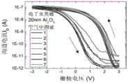
图2为本发明实施例1的比较例1的薄膜晶体管的迟滞曲线测试结果。2 is a test result of a hysteresis curve of the thin film transistor of Comparative Example 1 of Example 1 of the present invention.
图3为本发明实施例1的比较例2的薄膜晶体管的迟滞曲线测试结果。3 is a test result of a hysteresis curve of the thin film transistor of Comparative Example 2 of Example 1 of the present invention.
图4为本发明实施例1的比较例3的薄膜晶体管的迟滞曲线测试结果。FIG. 4 is a test result of a hysteresis curve of the thin film transistor of Comparative Example 3 of Example 1 of the present invention.
图5为本发明实施例1的比较例4的薄膜晶体管的迟滞曲线测试结果。5 is a test result of a hysteresis curve of the thin film transistor of Comparative Example 4 of Example 1 of the present invention.
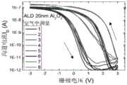
图6为本发明实施例1提供的薄膜晶体管的迟滞曲线测试结果。FIG. 6 is a test result of a hysteresis curve of the thin film transistor provided in
图7为本发明实施例2提供的薄膜晶体管的结构示意图。FIG. 7 is a schematic structural diagram of a thin film transistor provided in
图8为本发明实施例2的比较例5的薄膜晶体管的迟滞曲线测试结果。FIG. 8 is a test result of a hysteresis curve of the thin film transistor of Comparative Example 5 of Example 2 of the present invention.
图9为本发明实施例2的比较例6的薄膜晶体管的迟滞曲线测试结果。FIG. 9 is a test result of a hysteresis curve of the thin film transistor of Comparative Example 6 of Example 2 of the present invention.
图10为本发明实施例2提供的薄膜晶体管的迟滞曲线测试结果。FIG. 10 is a test result of a hysteresis curve of the thin film transistor provided in
图11为本发明实施例3提供的薄膜晶体管的结构示意图。FIG. 11 is a schematic structural diagram of a thin film transistor provided in
图12为本发明实施例3的比较例7的薄膜晶体管的迟滞曲线测试结果。12 is a test result of a hysteresis curve of the thin film transistor of Comparative Example 7 of Example 3 of the present invention.
图13为本发明实施例3提供的薄膜晶体管的迟滞曲线测试结果。FIG. 13 is a test result of the hysteresis curve of the thin film transistor provided in
图14为本发明实施例3提供的薄膜晶体管的迟滞曲线消除的稳定性进行测试结果。FIG. 14 is a test result of the stability of elimination of the hysteresis curve of the thin film transistor provided in
图15为本发明实施例4的比较例8的薄膜晶体管的迟滞曲线测试结果。15 is a test result of a hysteresis curve of the thin film transistor of Comparative Example 8 of Example 4 of the present invention.
图16为本发明实施例4提供的薄膜晶体管的迟滞曲线测试结果。FIG. 16 is a test result of a hysteresis curve of the thin film transistor provided in
图17为本发明实施例5提供的薄膜晶体管的结构示意图。FIG. 17 is a schematic structural diagram of a thin film transistor provided in
图18为本发明实施例5的比较例9的薄膜晶体管的迟滞曲线测试结果。18 is a test result of a hysteresis curve of the thin film transistor of Comparative Example 9 of Example 5 of the present invention.
图19为本发明实施例5提供的薄膜晶体管的迟滞曲线测试结果。FIG. 19 is a test result of a hysteresis curve of the thin film transistor provided in
图20为本发明实施例5的比较例9的薄膜晶体管的输出特性测试结果。FIG. 20 is the output characteristic test result of the thin film transistor of Comparative Example 9 of Example 5 of the present invention.
图21为本发明实施例5提供的薄膜晶体管的输出特性测试结果。FIG. 21 is a test result of the output characteristics of the thin film transistor provided in
图22为本发明实施例6的比较例10的薄膜晶体管的迟滞曲线测试结果。22 is a test result of a hysteresis curve of the thin film transistor of Comparative Example 10 of Example 6 of the present invention.
图23为本发明实施例6的比较例11的薄膜晶体管的迟滞曲线测试结果。23 is a test result of a hysteresis curve of the thin film transistor of Comparative Example 11 of Example 6 of the present invention.
图24为本发明实施例6提供的薄膜晶体管的迟滞曲线测试结果。FIG. 24 is a test result of the hysteresis curve of the thin film transistor provided in
图25为本发明实施例7的比较例12的薄膜晶体管的迟滞曲线测试结果。25 is a test result of a hysteresis curve of the thin film transistor of Comparative Example 12 of Example 7 of the present invention.
图26为本发明实施例7提供的薄膜晶体管的迟滞曲线测试结果。FIG. 26 is a test result of the hysteresis curve of the thin film transistor provided in
图27为本发明实施例8的比较例14的薄膜晶体管的迟滞曲线测试结果。27 is a test result of a hysteresis curve of the thin film transistor of Comparative Example 14 of Example 8 of the present invention.
图28为本发明实施例8提供的薄膜晶体管的迟滞曲线测试结果。FIG. 28 is a test result of the hysteresis curve of the thin film transistor provided in
图29为本发明实施例9的比较例15的薄膜晶体管的迟滞曲线测试结果。29 is a test result of a hysteresis curve of the thin film transistor of Comparative Example 15 of Example 9 of the present invention.
图30为本发明实施例9的比较例16的薄膜晶体管的迟滞曲线测试结果。30 is a test result of a hysteresis curve of the thin film transistor of Comparative Example 16 of Example 9 of the present invention.
图31为本发明实施例9提供的薄膜晶体管的迟滞曲线测试结果。FIG. 31 is a test result of the hysteresis curve of the thin film transistor provided in
图32为本发明实施例10的比较例17的薄膜晶体管的迟滞曲线测试结果。32 is a test result of a hysteresis curve of the thin film transistor of Comparative Example 17 of Example 10 of the present invention.
图33为本发明实施例10提供的薄膜晶体管的迟滞曲线测试结果。FIG. 33 is a test result of a hysteresis curve of the thin film transistor provided in
图34为本发明实施例11提供的薄膜晶体管的迟滞曲线测试结果。FIG. 34 is a test result of the hysteresis curve of the thin film transistor provided in
图35为本发明实施例12提供的逻辑电路的结构示意图。FIG. 35 is a schematic structural diagram of a logic circuit provided in
图36为本发明实施例12的比较例18的逻辑电路的输入输出特性曲线。36 is an input-output characteristic curve of the logic circuit of Comparative Example 18 of
图37为本发明实施例12提供的逻辑电路的输入输出特性曲线。FIG. 37 is an input-output characteristic curve of the logic circuit provided in
图38为本发明实施例12和比较例18的逻辑电路的在输入频率为0.1kHz的频率输出响应结果。FIG. 38 is the frequency output response results of the logic circuits of Example 12 and Comparative Example 18 of the present invention at an input frequency of 0.1 kHz.
图39为本发明实施例12和比较例18的逻辑电路的在输入频率为1kHz的频率输出响应结果。FIG. 39 shows the frequency output response results of the logic circuits of Example 12 and Comparative Example 18 of the present invention at an input frequency of 1 kHz.
图40为图39的单一周期的频率输出波形的放大图。FIG. 40 is an enlarged view of the single-cycle frequency output waveform of FIG. 39 .
图41为本发明实施例13提供的逻辑电路的结构示意图。FIG. 41 is a schematic structural diagram of a logic circuit provided in
图42为本发明实施例14提供的逻辑电路的结构示意图。FIG. 42 is a schematic structural diagram of a logic circuit provided in
主要元件符号说明Description of main component symbols
逻辑电路 10,10A,10B
薄膜晶体管 100,100A,100B,100C
基底 101
栅极 102
电介质层 103,103a,103b
第一子电介质层 1031,1031a,1031bfirst
第二子电介质层 1032,1032a,1032bSecond
半导体层 104,104a,104bSemiconductor layers 104, 104a, 104b
源极 105,105a,105b
漏极 106,106a,106b
具体实施方式Detailed ways
下面将结合附图及具体实施例对本发明作进一步的详细说明。The present invention will be further described in detail below with reference to the accompanying drawings and specific embodiments.
实施例1Example 1
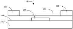
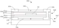
请参阅图1,本发明实施例1提供一种薄膜晶体管100,所述薄膜晶体管100为底栅型,其包括一基底101、一栅极102、一电介质层103、一半导体层104、一源极105和一漏极106。所述栅极102设置于所述基底101的一表面。所述电介质层103设置于所述基底101上且将所述栅极102覆盖。所述半导体层104设置于所述电介质层103远离所述基底101的表面。所述源极105和漏极106间隔设置于所述电介质层103远离所述基底101的一侧,且分别与所述半导体层104电连接。所述半导体层104位于所述源极105和漏极106之间的部分形成一沟道层。Referring to FIG. 1,
所述基底101用于支撑所述栅极102、电介质层103、半导体层104、源极105和漏极106。所述基底101的尺寸和形状不限,可以根据需要选择。所述基底101的材料可以为绝缘材料,例如玻璃、聚合物、陶瓷或石英等。所述基底101也可以为设置有绝缘层的半导体基底或导电基底。本实施例中,所述基底101为一具有二氧化硅绝缘层的硅片。The
所述电介质层103为采用磁控溅射法制备的氧化物层,且与所述栅极102直接接触。所述电介质层103的厚度为10纳米~1000纳米。所述氧化物可以为金属氧化物,例如,Al2O3,也可以为硅氧化物,例如,SiO2。本实施例中,所述电介质层103为采用磁控溅射法制备的厚度40纳米的SiO2层。The
所述半导体层104包括多个纳米半导体材料。所述纳米半导体材料可以为石墨烯、碳纳米管、MoS2、WS2、MnO2、ZnO、MoSe2、MoTe2、TaSe2、NiTe2、Bi2Te3等。所述纳米半导体材料通过生长、转移、沉积或旋涂等方法形成于所述电介质层103表面。所述半导体层104为单层或少层纳米半导体材料,例如1~5层。本实施例中,所述半导体层104为通过沉积单壁碳纳米管形成单壁碳纳米管网络制备而成。The
所述栅极102、源极105和漏极106由导电材料制备,其制备方法可以为化学蒸镀、电子束蒸发、热沉积或磁控溅射等。优选地,所述栅极102、源极105和漏极106为一层导电薄膜。该导电薄膜的厚度为0.5纳米~100微米。该导电薄膜的材料为金属,如铝、铜、钨、钼、金、钛、钕、钯、铯等。可以理解,所述栅极102、源极105和漏极106的材料也可为导电浆料、ITO、碳纳米管或石墨烯等。本实施例中,所述栅极102、源极105和漏极106的材料为钛金复合金属层,厚度为40纳米。The
所述薄膜晶体管100的制备方法包括以下步骤:The preparation method of the
步骤S11,提供一基底101;Step S11, providing a
步骤S12,在所述基底101表面沉积一栅极102;Step S12, depositing a
步骤S13,在所述基底101表面采用磁控溅射法制备一氧化物层作为电介质层103,且所述氧化物层将所述栅极102覆盖且与所述栅极102直接接触;Step S13, an oxide layer is prepared on the surface of the
步骤S14,在所述电介质层103表面制备一半导体层104,所述半导体层104包括多个纳米材料;Step S14, preparing a
步骤S15,在所述电介质层103表面制备源极105和漏极106,且所述源极105和漏极106与所述半导体层104电连接。In step S15 , a
本实施例中,所述步骤S13中,在所述基底101表面采用磁控溅射法制备SiO2层。所述磁控溅射的溅射靶与样品距离可以为50毫米~120毫米,溅射前的真空度为小于10-5Pa,溅射的功率可以为150瓦~200瓦,载气为氩气,溅射时的压强可以为0.2帕~1帕。本实施例分别采用不同的工艺参数制备厚度为10纳米、20纳米、100纳米、500纳米、1000纳米的SiO2层作为电介质层103,结果均表明采用磁控溅射法制备SiO2层为反常迟滞材料。In this embodiment, in the step S13 , a SiO2 layer is prepared on the surface of the
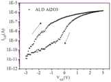
为了研究采用磁控溅射法制备的SiO2层作为电介质层103对所述薄膜晶体管100的迟滞曲线的反常影响,本实施例还分别制备了采用正常迟滞材料的比较例1-4。比较例与本实施例的区别仅为所述电介质层103的材料和制备方法。其中,比较例1采用电子束蒸发20纳米SiO2层作为电介质层103,比较例2采用电子束蒸发20纳米Al2O3层作为电介质层103,比较例3采用ALD法沉积20纳米Al2O3层作为电介质层103,比较例3采用ALD法沉积20纳米HfO2层作为电介质层103。比较结果参见表1。In order to study the abnormal influence of the SiO2 layer prepared by magnetron sputtering as the
表1实施例1与比较例的工艺参数以及测试结果对比Table 1 Comparison of process parameters and test results between Example 1 and Comparative Example

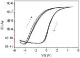
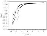
本实施例的薄膜晶体管100进行测量时,所述半导体层104暴露在空气中。比较例1-4以及本实施例的薄膜晶体管100均为P型。参见图2-6,分别为比较例1-4以及本实施例的薄膜晶体管100的迟滞曲线测试结果。其中,图2-5分别给出了多个比较样品的测试结果。进一步参见表1可见,比较例1-4的薄膜晶体管100的迟滞曲线均表现为逆时针,而本实施例的薄膜晶体管100的迟滞曲线表现为顺时针。由比较例1和本实施例可知,在底栅型薄膜晶体管100中,采用磁控溅射法制备的SiO2层作为电介质层103可以得到反常迟滞曲线。When the
实施例2Example 2
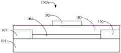
请参阅图7,本发明实施例2提供一种薄膜晶体管100A,其包括一基底101、一栅极102、一电介质层103、一半导体层104、一源极105和一漏极106。所述半导体层104设置于所述基底101的一表面。所述源极105和漏极106间隔设置于所述基底101上,且分别与所述半导体层104电连接。所述半导体层104位于所述源极105和漏极106之间的部分形成一沟道层。所述电介质层103设置于所述半导体层104远离所述基底101的表面,且将所述半导体层104、源极105和漏极106覆盖。所述栅极102设置于所述电介质层103远离所述基底101的表面。Referring to FIG. 7 ,
本发明实施例2的薄膜晶体管100A与本发明实施例1的薄膜晶体管100结构基本相同,其区别为,所述薄膜晶体管100A为顶栅型。所述薄膜晶体管100A的制备方法包括以下步骤:The
步骤S21,提供一基底101;Step S21, providing a
步骤S22,在所述基底101表面制备一半导体层104,所述半导体层104包括多个纳米材料;Step S22, preparing a
步骤S23,在所述基底101上制备源极105和漏极106,且所述源极105和漏极106与所述半导体层104电连接;Step S23, preparing a
步骤S24,在所述半导体层104远离所述基底101的表面采用磁控溅射法制备一氧化物层作为电介质层103,且所述氧化物层将所述半导体层104、源极105和漏极106覆盖;In step S24, an oxide layer is prepared on the surface of the
步骤S25,在所述电介质层103远离所述基底101的表面制备一栅极102,且所述栅极102与所述电介质层103直接接触。In step S25 , a
为了研究采用磁控溅射法制备的SiO2层作为电介质层103对所述薄膜晶体管100A的迟滞曲线的影响,本实施例还分别制备了采用正常迟滞材料的比较例5-6。比较例与本实施例的区别仅为所述电介质层103的材料和制备方法。其中,比较例5采用电子束蒸发20纳米SiO2层作为电介质层103,比较例6采用热氧化法制备20纳米Y2O3层作为电介质层103。比较结果参见表2。In order to study the influence of the SiO2 layer prepared by the magnetron sputtering method as the
表2实施例2与比较例的工艺参数以及测试结果对比The process parameters and test results of table 2

本实施例的薄膜晶体管100A进行测量。比较例5-6以及本实施例的薄膜晶体管100A为P型。参见图8-9,比较例5-6的薄膜晶体管100A的迟滞曲线表现为逆时针。参见图10,本实施例的薄膜晶体管100A的迟滞曲线表现为顺时针,即迟滞反常。由比较例5-6和本实施例可知,在顶栅型薄膜晶体管100A中,采用磁控溅射法制备的SiO2层作为电介质层103可以得到反常迟滞曲线,而且保持薄膜晶体管100A的极性不变。The
实施例3Example 3
请参阅图11,本发明实施例3提供一种薄膜晶体管100B,其包括一基底101、一栅极102、一电介质层103、一半导体层104、一源极105和一漏极106。所述栅极102设置于所述基底101的一表面。所述电介质层103设置于所述基底101上且将所述栅极102覆盖。所述半导体层104设置于所述电介质层103远离所述基底101的表面。所述源极105和漏极106间隔设置于所述电介质层103远离所述基底101的一侧,且分别与所述半导体层104电连接。所述半导体层104位于所述源极105和漏极106之间的部分形成一沟道层。所述薄膜晶体管100B也为底栅型。Referring to FIG. 11 ,
本发明实施例3的薄膜晶体管100B与本发明实施例1的薄膜晶体管100结构基本相同,其区别为,所述电介质层103为双层结构,其包括层叠设置的第一子电介质层1031和第二子电介质层1032。所述第一子电介质层1031为反常迟滞材料层,即采用磁控溅射法制备的SiO2层。所述第二子电介质层1032为正常迟滞材料层。所述薄膜晶体管100B的制备方法包括以下步骤:The
步骤S31,提供一基底101;Step S31, providing a
步骤S32,在所述基底101表面沉积一栅极102;Step S32, depositing a
步骤S33,在所述基底101表面采用磁控溅射法制备一SiO2层作为第一子电介质层1031,且所述SiO2层将所述栅极102覆盖且与所述栅极102直接接触;Step S33, a SiO2 layer is prepared on the surface of the
步骤S34,在所述第一子电介质层1031表面制备一正常迟滞材料层作为第二子电介质层1032,从而得到一双层结构的电介质层103;Step S34, preparing a normal hysteresis material layer on the surface of the first
步骤S35,在所述电介质层103表面制备一半导体层104,所述半导体层104包括多个纳米材料;Step S35, preparing a
步骤S36,在所述电介质层103表面制备源极105和漏极106,且所述源极105和漏极106与所述半导体层104电连接。In step S36 , a
本实施例中,所述第二子电介质层1032的正常迟滞材料层为采用ALD法沉积的20纳米厚的Al2O3层。为了研究采用磁控溅射法制备的SiO2反常迟滞材料层对正常迟滞材料层的迟滞曲线的影响,本实施例还还制备比较例7。比较例7与本实施例的区别仅为:所述第一子电介质层1031为采用ALD法沉积的20纳米厚的Al2O3正常迟滞材料,而第二子电介质层1032为反常迟滞材料层。比较结果参见表3。In this embodiment, the normal hysteresis material layer of the second
表3实施例3与比较例的工艺参数以及测试结果对比The process parameters and test results of table 3

本实施例的薄膜晶体管100B进行测量。比较例7以及本实施例的薄膜晶体管100B均为P型。参见图12和图4可见,比较例7的薄膜晶体管的迟滞曲线与比较例3的薄膜晶体管的迟滞曲线基本相同。由此可见,比较例7中,采用磁控溅射法制备的SiO2对薄膜晶体管的迟滞曲线几乎没有影响。参见图13,实施例3的薄膜晶体管100B的迟滞曲线被明显减小甚至消除。对比比较例7和实施例3可见,只有当反常迟滞材料层直接与栅极102接触,起到调制沟道层作用时,所述反常迟滞材料层才会产生反常迟滞曲线。实施例3中,所述反常迟滞材料层的顺时针迟滞曲线与正常迟滞材料层的逆时针迟滞曲线相互抵消,从而起到消除薄膜晶体管的迟滞曲线的作用。The
进一步,本发明对实施例3的薄膜晶体管100B的迟滞曲线消除的稳定性进行测试。参见图14,60天之后,实施例3的薄膜晶体管100B的迟滞曲线与之前基本吻合。由此可见,该结构可以稳定消除TFT迟滞曲线。Further, the present invention tests the stability of the elimination of the hysteresis curve of the
实施例4Example 4
本发明实施例4的薄膜晶体管100B与本发明实施例3的薄膜晶体管100B结构基本相同,其区别为,所述第一子电介质层1031为反常迟滞材料层,采用磁控溅射法制备的SiO2层;所述第二子电介质层1032为正常迟滞材料层,采用电子束蒸发法制备的SiO2层。The
本实施例还还制备比较例8。比较例8与本实施例的区别仅为:所述第一子电介质层1031为正常迟滞材料,而第二子电介质层1032为反常迟滞材料层。比较结果参见表4。Comparative Example 8 was also prepared in this example. The difference between the comparative example 8 and the present embodiment is only that the first
表4实施例4与比较例的工艺参数以及测试结果对比The process parameters and test results of table 4

本实施例的薄膜晶体管100B进行测量。比较例8以及本实施例的薄膜晶体管100B均为P型。参见图15,比较例8的薄膜晶体管具有明显的迟滞曲线。参见图16,实施例4的薄膜晶体管100B的迟滞曲线被明显减小甚至消除。由本实施例、比较例1和比较例8可以看出,电子束蒸镀制备SiO2为正常迟滞材料,而采用磁控溅射法制备的SiO2层为反常迟滞材料。而且,只有当反常迟滞材料层直接与栅极102接触,起到调制沟道层作用时,所述反常迟滞材料层才会产生反常迟滞曲线。The
实施例5Example 5
请参阅图17,本发明实施例5提供一种薄膜晶体管100C,其包括一基底101、一栅极102、一电介质层103、一半导体层104、一源极105和一漏极106。所述半导体层104设置于所述基底101的一表面。所述源极105和漏极106间隔设置于所述基底101上,且分别与所述半导体层104电连接。所述半导体层104位于所述源极105和漏极106之间的部分形成一沟道层。所述电介质层103设置于所述半导体层104远离所述基底101的表面,且将所述半导体层104、源极105和漏极106覆盖。所述栅极102设置于所述电介质层103远离所述基底101的表面。所述薄膜晶体管100C为顶栅型。Referring to FIG. 17 ,
本发明实施例5的薄膜晶体管100C与本发明实施例2的薄膜晶体管100A结构基本相同,其区别为,所述电介质层103为双层结构,其包括层叠设置的第一子电介质层1031和第二子电介质层1032。所述第一子电介质层1031为反常迟滞材料层,即采用磁控溅射法制备的SiO2层。所述第二子电介质层1032为正常迟滞材料层。所述薄膜晶体管100C的制备方法包括以下步骤:The
步骤S51,提供一基底101;Step S51, providing a
步骤S52,在所述基底101表面制备一半导体层104,所述半导体层104包括多个纳米材料;Step S52, preparing a
步骤S53,在所述基底101上制备源极105和漏极106,且所述源极105和漏极106与所述半导体层104电连接;Step S53, preparing a
步骤S54,在所述半导体层104远离所述基底101的表面制备一正常迟滞材料层作为第二子电介质层1032,所述第二子电介质层1032将所述半导体层104、源极105和漏极106覆盖;Step S54, a normal hysteresis material layer is prepared on the surface of the
步骤S55,在所述第二子电介质层1032远离所述基底101的表面采用磁控溅射法制备一SiO2层作为第一子电介质层1031,所述第一子电介质层1031将所述第二子电介质层1032覆盖,从而形成电介质层103;Step S55 , a SiO2 layer is prepared on the surface of the second
步骤S56,在所述电介质层103远离所述基底101的表面制备一栅极102,In step S56, a
且所述栅极102与所述第一子电介质层1031直接接触。And the
本实施例中,所述第二子电介质层1032的正常迟滞材料层为采用热氧化法制备5纳米Y2O3层。为了研究采用磁控溅射法制备的SiO2反常迟滞材料层对正常迟滞材料层的迟滞曲线的影响,本实施例还还制备比较例9。比较例9与本实施例的区别仅为:所述第一子电介质层1031为采用热氧化法制备的20纳厚度的Y2O3正常迟滞材料,而第二子电介质层1032为反常迟滞材料层。比较结果参见表5。In this embodiment, the normal hysteresis material layer of the second
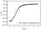
表5实施例5与比较例的工艺参数以及测试结果对比Table 5 Process parameter and test result comparison of

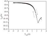
本实施例的薄膜晶体管100C进行测量。比较例9以及本实施例的薄膜晶体管100C为P型。参见图18,比较例9的薄膜晶体管具有明显的迟滞曲线。参见图19,当采用磁控溅射法制备的SiO2反常迟滞材料层与所述栅极102直接接触设置时,薄膜晶体管100C的迟滞曲线被明显减小甚至消除。The
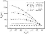
进一步,对比较例9以及本实施例的薄膜晶体管100C的输出特性进行测试。输出特性曲线为一组随着栅极电压VG不同,导致漏电流ID随漏电压VD变化的曲线。参见图20,对比较例9的薄膜晶体管100C,由于具有迟滞,VG从0V扫描至-3V,与从-3V扫描至0V,在相同的VG下(相同线条)曲线不重合。参见图21,对本实施例的薄膜晶体管100C,有于没有迟滞,即使VG的扫描方向不同,其对应的ID-VD曲线是基本重合的。这对于TFT在逻辑电路、传感器等方面的应用是很重要的。Further, the output characteristics of the
实施例6Example 6
本发明实施例6的薄膜晶体管100C与本发明实施例5的薄膜晶体管100C结构基本相同,其区别为,所述第一子电介质层1031为反常迟滞材料层,采用磁控溅射法制备的SiO2层;所述第二子电介质层1032为正常迟滞材料层,采用ALD法制备的Al2O3层。由于隔绝空气和固定电荷掺杂,实施例6的薄膜晶体管100C成为双极型。The
本实施例还还制备比较例10-11。比较例10与本实施例的区别仅为:所述电介质层103为如图7所示的单层结构,且所述电介质层103也为采用ALD法制备的Al2O3层。比较例11与本实施例的区别仅为:所述第一子电介质层1031为正常迟滞材料,而第二子电介质层1032为反常迟滞材料层。比较结果参见表6。Comparative Examples 10-11 were also prepared in this example. The difference between the comparative example 10 and the present embodiment is only that the
表6实施例6与比较例的工艺参数以及测试给果对比The technological parameters of table 6

本实施例的薄膜晶体管100C进行测量。比较例10-11以及本实施例的薄膜晶体管100C为双极型。参见图22和图23,当采用磁控溅射法制备的SiO2反常迟滞材料层与所述栅极102间隔设置时,对薄膜晶体管的迟滞曲线几乎没有影响。参见图24,当采用磁控溅射法制备的SiO2反常迟滞材料层与所述栅极102直接接触设置时,薄膜晶体管100C的迟滞曲线被明显减小甚至消除。The
实施例7Example 7
本发明实施例7的薄膜晶体管100C与本发明实施例5的薄膜晶体管100C结构基本相同,其区别为,所述第一子电介质层1031为反常迟滞材料层,采用磁控溅射法制备的SiO2层;所述第二子电介质层1032为正常迟滞材料层,采用PECVD法制备的Si3N4层。The
本实施例还还制备比较例12-13。比较例12与本实施例的区别仅为:所述电介质层103为如图7所示的单层结构,且所述电介质层103也为采用PECVD法制备的Si3N4层。比较例13与本实施例的区别仅为:所述第一子电介质层1031为正常迟滞材料,而第二子电介质层1032为反常迟滞材料层。比较结果参见表7。This example also prepared Comparative Examples 12-13. The difference between Comparative Example 12 and this embodiment is only that the
表7实施例7与比较例的工艺参数以及测试结果对比Table 7 Process parameter and test result comparison of

本实施例的薄膜晶体管100C进行测量。比较例12和本实施例的薄膜晶体管100C为N型。比较例13的薄膜晶体管为双极型。由于比较例13的结构无法得到N型薄膜晶体管,因此,本实施例与比较例13的迟滞曲线没有比较意义。由于P型和N型的区别,导致P型的正常迟滞为逆时针,而N型的正常迟滞为顺时针,但迟滞曲线本质是一样的。参见图25和图26,相较于比较例12的采用PECVD法制备的单层Si3N4正常迟滞材料层的薄膜晶体管,采用磁控溅射法制备的SiO2反常迟滞材料层,且反常迟滞材料层与所述栅极102直接接触设置,薄膜晶体管100C的迟滞曲线被明显减小甚至消除。The
实施例8Example 8
本发明实施例8的薄膜晶体管100C与本发明实施例5的薄膜晶体管100C结构基本相同,其区别为,所述第一子电介质层1031为反常迟滞材料层,采用磁控溅射法制备的SiO2层;所述第二子电介质层1032为正常迟滞材料层,采用电子束蒸发法制备的SiO2层。The
本实施例还制备比较例14。比较例14与本实施例的区别仅为:所述第一子电介质层1031为正常迟滞材料,而第二子电介质层1032为反常迟滞材料层。比较结果参见表8。This example also prepared Comparative Example 14. The difference between the comparative example 14 and the present embodiment is only that the first
表8实施例8与比较例的工艺参数以及测试结果对比Table 8 Process parameters and test results comparison of Example 8 and Comparative Example

本实施例的薄膜晶体管100C进行测量。比较例14和本实施例的薄膜晶体管100C为P型。参见图27,比较例14的薄膜晶体管具有明显的迟滞曲线。参见图28,实施例8的薄膜晶体管100C的迟滞曲线被明显减小甚至消除。The
实施例9Example 9
本发明实施例9的薄膜晶体管100A与本发明实施例2的薄膜晶体管100A结构基本相同,其区别为,所述半导体层104采用二硫化钼二维纳米材料制备。The
本实施例还制备比较例15-16。比较例15与本实施例的区别仅为:薄膜晶体管结构为100,所述电介质层103为采用热氧化法制备的SiO2层。比较例16与本实施例的区别仅为:所述电介质层103为采用ALD法制备的Al2O3层。比较结果参见表9。This example also prepared Comparative Examples 15-16. The difference between the comparative example 15 and the present embodiment is only: the thin film transistor structure is 100, and the
表9实施例9与比较例的工艺参数以及测试结果对比Table 9 Process parameter and test result comparison of

本实施例的薄膜晶体管100A进行测量。比较例15-16和本实施例的薄膜晶体管100A为N型。参见图29-30,比较例15-16的薄膜晶体管100A的正常迟滞曲线为顺时针。参见图31,本实施例的薄膜晶体管100A的迟滞曲线为逆时针,即反常迟滞曲线。由此可见,即使采用其他低维纳米半导体材料薄膜,采用磁控溅射法制备的氧化物层仍然具有反常迟滞曲线为作用。The
实施例10Example 10
本发明实施例10的薄膜晶体管100C与本发明实施例5的薄膜晶体管100C结构基本相同,其区别为,所述第一子电介质层1031为反常迟滞材料层,采用磁控溅射法制备的SiO2层;所述第二子电介质层1032为正常迟滞材料层,采用ALD法制备的Al2O3层。The
本实施例还制备比较例17。比较例17与本实施例的区别仅为:所述第一子电介质层1031为正常迟滞材料,而第二子电介质层1032为反常迟滞材料层。比较结果参见表10。This example also prepared Comparative Example 17. The difference between the comparative example 17 and the present embodiment is only that the first
表10实施例10与比较例的工艺参数以及测试结果对比Table 10 Process parameter and test result comparison of

本实施例的薄膜晶体管100C进行测量。比较例17和本实施例的薄膜晶体管100C为N型。参见图32,比较例17的薄膜晶体管具有明显的迟滞曲线,且与比较例16迟滞曲线基本相同。参见图33,实施例10的薄膜晶体管100C的迟滞曲线被明显减小甚至消除。The
实施例11Example 11
本发明实施例11的薄膜晶体管100与本发明实施例1的薄膜晶体管100结构基本相同,其区别为,所述电介质层103为采用磁控溅射法制备的Al2O3层。本实施例分别采用不同的磁控溅射工艺参数制备厚度为10纳米、20纳米、100纳米、500纳米、1000纳米的Al2O3层作为电介质层103,结果均表明采用磁控溅射法制备的Al2O3层为反常迟滞材料。本实施例中,将实施例11的薄膜晶体管100与上述比较例2-3进行比较,结果参见表11。The
表11实施例11与比较例的工艺参数以及测试结果对比Table 11 Comparison of process parameters and test results of Example 11 and Comparative Example

本实施例的薄膜晶体管100进行测量。本实施例的薄膜晶体管100为P型。参见图34和图3-4可见,本实施例的薄膜晶体管100的迟滞曲线为顺时针,即反常迟滞曲线。可以理解,采用磁控溅射法制备的Al2O3层为反常迟滞材料与其他正常迟滞材料形成双层电介质层103,且使所述栅极102与所述反常迟滞材料层直接接触,同样可以起到减小或消除迟滞曲线的作用。The
实施例12Example 12
请参阅图35,本发明实施例12提供一种采用上述减小或消除迟滞曲线的薄膜晶体管100C的逻辑电路10。所述逻辑电路10包括两个双极性的顶栅型薄膜晶体管100C,且每个薄膜晶体管100C包括一基底101、一栅极102、一电介质层103、一半导体层104、一源极105和一漏极106。所述电介质层103为双层结构,其包括层叠设置的第一子电介质层1031和第二子电介质层1032。所述两个双极性的薄膜晶体管100C的栅极102电连接,且所述两个双极性的薄膜晶体管100C的源极105或漏极106电连接。可以理解,本实施例中,所述逻辑电路10为一反向器。Referring to FIG. 35 ,
具体地,所述两个双极性的薄膜晶体管100C共用一个基底101、共用一个漏极106、且共用一个栅极102。所述两个双极性的薄膜晶体管100C的半导体层104可以通过图案化一连续的碳纳米管层制备。所述两个双极性的薄膜晶体管100C的第一子电介质层1031或第二子电介质层1032均为一次沉积制备的连续整体结构。所述第一子电介质层1031为采用磁控溅射法制备的SiO2反常迟滞材料层。所述第二子电介质层1032为采用ALD法制备的Al2O3正常迟滞材料层。Specifically, the two bipolar
本实施例还制备比较例18。比较例18与本实施例的区别仅为:所述第一子电介质层1031为正常迟滞材料,而第二子电介质层1032为反常迟滞材料层。比较结果参见表12。This example also prepared Comparative Example 18. The difference between the comparative example 18 and the present embodiment is only that the first
表12实施例12与比较例的工艺参数以及测试结果对比Table 12 Comparison of process parameters and test results of Example 12 and Comparative Example

本实施例对所述逻辑电路10的输入输出特性进行测试。参见图36,比较例18的逻辑电路10的转换阈值的差别达到1V以上。参见图37,本实施例的逻辑电路10的转换阈值的差别在0.1V左右。In this embodiment, the input and output characteristics of the
本实施例还对所述逻辑电路10的频率响应特性进行测试。实验中,比较例18和本实施例的逻辑电路10的开态电流相同,以保证单个器件的迁移率相同,从而比较迟滞对于频率响应的影响。参见图38和39,为输入频率为0.1kHz和1kHz时,比较例18和本实施例的逻辑电路10的输出响应。由图38可见,输入频率为0.1kHz时,比较例18的逻辑电路10在低电平不稳定,而本实施例的逻辑电路10输出反相方波性能良好。由图39可见,输入频率为1kHz时,本实施例的逻辑电路10仍然能正常工作,而比较例18的逻辑电路10则已经完全没有了低电平,上升沿下降沿延迟时间都明显大于本实施例的逻辑电路10。In this embodiment, the frequency response characteristic of the
参见图40,通过放大图38的单一周期的频率输出波形,可以看到,本实施例的逻辑电路10上升沿与下降沿的延迟时间均小于比较例18的逻辑电路10。通过截止工作频率计算公式f=1/(2*max(tr,tf)),可以得出在单个器件延迟时间类似的情况下,本实施例的逻辑电路10的截止工作频率比比较例18的逻辑电路10高将近5倍。以上实验结果说明了TFT迟滞对于逻辑电路稳定性以及频率响应特性都存在很大的影响。因此消除迟滞是非常必要的。而且,本发明通过消除迟滞,极大改善了逻辑电路10的电学性能。Referring to FIG. 40 , by enlarging the single-cycle frequency output waveform of FIG. 38 , it can be seen that the delay time of the rising edge and the falling edge of the
实施例13Example 13
请参阅图41,本发明实施例13提供一种采用上述减小或消除迟滞曲线的薄膜晶体管100C的逻辑电路10A。所述逻辑电路10A包括一个N型的顶栅型薄膜晶体管100C和一个P型的顶栅型薄膜晶体管100C。所述N型薄膜晶体管100C包括一基底101、一栅极102、一电介质层103a、一半导体层104a、一源极105a和一漏极106。所述电介质层103a为双层结构,其包括层叠设置的第一子电介质层1031和第二子电介质层1032a。所述P型薄膜晶体管100C包括一基底101、一栅极102、一电介质层103b、一半导体层104b、一源极105b和一漏极106。所述电介质层103b为双层结构,其包括层叠设置的第一子电介质层1031和第二子电介质层1032b。所述N型薄膜晶体管100C和P型薄膜晶体管100C的栅极102电连接,且源极105或漏极106电连接。可以理解,本实施例中,所述逻辑电路10也为一反向器。Referring to FIG. 41 ,
具体地,所述N型薄膜晶体管100C和P型薄膜晶体管100C共面设置,共用一个基底101、共用一个漏极106、且共用一个栅极102。所述N型薄膜晶体管100C和P型薄膜晶体管100C的半导体层104可以通过图案化一连续的碳纳米管层制备。所述N型薄膜晶体管100C和P型薄膜晶体管100C的第一子电介质层1031为一次沉积制备的连续整体结构。所述N型薄膜晶体管100C的第二子电介质层1032a和P型薄膜晶体管100C的第二子电介质层1032b采用不同的正常迟滞材料层。所述第一子电介质层1031为采用磁控溅射法制备的SiO2反常迟滞材料层。所述第二子电介质层1032a为采用PECVD法制备的Si3N4正常迟滞材料层。所述第二子电介质层1032b为采用热氧化法制备的Y2O3正常迟滞材料层。Specifically, the N-type
实施例14Example 14
请参阅图42,本发明实施例14提供一种采用上述减小或消除迟滞曲线的薄膜晶体管100B和薄膜晶体管100C的逻辑电路10B。所述逻辑电路10B包括一个N型的顶栅型薄膜晶体管100C和一个P型的底栅极型薄膜晶体管100B。所述N型薄膜晶体管100C包括一基底101、一栅极102、一电介质层103a、一半导体层104a、一源极105a和一漏极106a。所述电介质层103a为双层结构,其包括层叠设置的第一子电介质层1031a和第二子电介质层1032a。所述P型薄膜晶体管100B包括一栅极102、一电介质层103b、一半导体层104b、一源极105b和一漏极106b。所述电介质层103b为双层结构,其包括层叠设置的第一子电介质层1031b和第二子电介质层1032b。所述N型薄膜晶体管100C和P型薄膜晶体管100B的栅极102电连接,且源极105a、105b或漏极106a、106b电连接。可以理解,本实施例中,所述逻辑电路10也为一反向器。Referring to FIG. 42 ,
具体地,所述N型薄膜晶体管100C和P型薄膜晶体管100B层叠设置,共用一个基底101、且共用一个栅极102。所述N型薄膜晶体管100C直接设置于所述基底101表面。所述电介质层1031a和电介质层103b具有一通孔,所述漏极106b延伸通过该通孔与所述漏极106a电连接。所述P型薄膜晶体管100B设置于所述第一子电介质层1031a表面。所述第一子电介质层1031a和电介质层1031b均为采用磁控溅射法制备的SiO2反常迟滞材料层。所述第二子电介质层1032a为采用PECVD法制备的Si3N4正常迟滞材料层。所述第二子电介质层1032b为采用ALD制备的Al2O3正常迟滞材料层。Specifically, the N-type
本发明具有以下优点:第一,采用磁控溅射法制备的氧化物材料作为电介质层可以得到具有反常迟滞曲线的薄膜晶体管;第二,采用正常迟滞材料和反常迟滞材料的双层电介质层结构可以减小甚至消除迟滞曲线;第三,采用减小或消除迟滞曲线的薄膜晶体管制备的逻辑器件具有优异的电学性能。The invention has the following advantages: firstly, a thin film transistor with anomalous hysteresis curve can be obtained by using the oxide material prepared by magnetron sputtering as a dielectric layer; secondly, a double-layer dielectric layer structure using normal hysteresis material and anomalous hysteresis material The hysteresis curve can be reduced or even eliminated; thirdly, the logic device prepared by using the thin film transistor with reduced or eliminated hysteresis curve has excellent electrical performance.
另外,本领域技术人员还可以在本发明精神内做其它变化,这些依据本发明精神所做的变化,都应包含在本发明所要求保护的范围内。In addition, those skilled in the art can also make other changes within the spirit of the present invention, and these changes made according to the spirit of the present invention should all be included within the scope of the claimed protection of the present invention.
Claims (8)
Priority Applications (4)
| Application Number | Priority Date | Filing Date | Title |
|---|---|---|---|
| CN201611114659.5ACN108172627B (en) | 2016-12-07 | 2016-12-07 | A kind of thin film transistor and preparation method thereof |
| TW105141974ATWI633672B (en) | 2016-12-07 | 2016-12-17 | Thin film transistor and preparation method thereof |
| US15/817,520US10431662B2 (en) | 2016-12-07 | 2017-11-20 | Thin film transistor and method for making the same |
| JP2017235363AJP6546645B2 (en) | 2016-12-07 | 2017-12-07 | Thin film transistor and method of manufacturing the same |
Applications Claiming Priority (1)
| Application Number | Priority Date | Filing Date | Title |
|---|---|---|---|
| CN201611114659.5ACN108172627B (en) | 2016-12-07 | 2016-12-07 | A kind of thin film transistor and preparation method thereof |
Publications (2)
| Publication Number | Publication Date |
|---|---|
| CN108172627A CN108172627A (en) | 2018-06-15 |
| CN108172627Btrue CN108172627B (en) | 2020-11-06 |
Family
ID=62243856
Family Applications (1)
| Application Number | Title | Priority Date | Filing Date |
|---|---|---|---|
| CN201611114659.5AActiveCN108172627B (en) | 2016-12-07 | 2016-12-07 | A kind of thin film transistor and preparation method thereof |
Country Status (4)
| Country | Link |
|---|---|
| US (1) | US10431662B2 (en) |
| JP (1) | JP6546645B2 (en) |
| CN (1) | CN108172627B (en) |
| TW (1) | TWI633672B (en) |
Families Citing this family (3)
| Publication number | Priority date | Publication date | Assignee | Title |
|---|---|---|---|---|
| US11222959B1 (en)* | 2016-05-20 | 2022-01-11 | Hrl Laboratories, Llc | Metal oxide semiconductor field effect transistor and method of manufacturing same |
| CN109273354B (en)* | 2018-09-07 | 2021-01-12 | 中国电子科技集团公司第十三研究所 | Diamond device and method for manufacturing same |
| CN110620043B (en)* | 2019-09-24 | 2021-01-15 | 山东大学 | Preparation method of semiconductor thin film field effect transistor made of unstable two-dimensional material |
Citations (3)
| Publication number | Priority date | Publication date | Assignee | Title |
|---|---|---|---|---|
| JP3696196B2 (en)* | 2002-11-01 | 2005-09-14 | 株式会社東芝 | Semiconductor device |
| CN102130009A (en)* | 2010-12-01 | 2011-07-20 | 北京大学深圳研究生院 | A method of manufacturing a transistor |
| CN104103695A (en)* | 2013-04-02 | 2014-10-15 | 清华大学 | Film transistor and preparation method thereof |
Family Cites Families (10)
| Publication number | Priority date | Publication date | Assignee | Title |
|---|---|---|---|---|
| US57102A (en)* | 1866-08-14 | Improved shoe-cleaner | ||
| DE10136756C2 (en)* | 2001-07-27 | 2003-07-31 | Siemens Ag | X-ray diagnostic device with a flexible solid-state X-ray detector |
| JP5471000B2 (en) | 2008-04-24 | 2014-04-16 | 東レ株式会社 | Field effect transistor |
| US20100137143A1 (en)* | 2008-10-22 | 2010-06-03 | Ion Torrent Systems Incorporated | Methods and apparatus for measuring analytes |
| JP5546794B2 (en)* | 2009-05-22 | 2014-07-09 | 富士フイルム株式会社 | FIELD EFFECT TRANSISTOR MANUFACTURING METHOD, FIELD EFFECT TRANSISTOR, AND DISPLAY DEVICE MANUFACTURING METHOD |
| KR101812683B1 (en) | 2009-10-21 | 2017-12-27 | 가부시키가이샤 한도오따이 에네루기 켄큐쇼 | Method for manufacturing semiconductor device |
| JP2011176168A (en) | 2010-02-25 | 2011-09-08 | Nippon Telegr & Teleph Corp <Ntt> | Semiconductor memory device |
| KR101980195B1 (en)* | 2012-05-16 | 2019-05-21 | 삼성전자주식회사 | Transistor having sulfur doped zinc oxynitride and method of manufacturing the same |
| CN102760749B (en)* | 2012-07-13 | 2016-04-13 | 京东方科技集团股份有限公司 | Luminescent device and preparation method thereof |
| CN105810748B (en) | 2014-12-31 | 2018-12-21 | 清华大学 | N-type TFT |
- 2016
- 2016-12-07CNCN201611114659.5Apatent/CN108172627B/enactiveActive
- 2016-12-17TWTW105141974Apatent/TWI633672B/enactive
- 2017
- 2017-11-20USUS15/817,520patent/US10431662B2/enactiveActive
- 2017-12-07JPJP2017235363Apatent/JP6546645B2/enactiveActive
Patent Citations (3)
| Publication number | Priority date | Publication date | Assignee | Title |
|---|---|---|---|---|
| JP3696196B2 (en)* | 2002-11-01 | 2005-09-14 | 株式会社東芝 | Semiconductor device |
| CN102130009A (en)* | 2010-12-01 | 2011-07-20 | 北京大学深圳研究生院 | A method of manufacturing a transistor |
| CN104103695A (en)* | 2013-04-02 | 2014-10-15 | 清华大学 | Film transistor and preparation method thereof |
Also Published As
| Publication number | Publication date |
|---|---|
| US10431662B2 (en) | 2019-10-01 |
| JP2018098501A (en) | 2018-06-21 |
| JP6546645B2 (en) | 2019-07-17 |
| TWI633672B (en) | 2018-08-21 |
| US20180158921A1 (en) | 2018-06-07 |
| CN108172627A (en) | 2018-06-15 |
| TW201822359A (en) | 2018-06-16 |
Similar Documents
| Publication | Publication Date | Title |
|---|---|---|
| CN108172612B (en) | Thin film transistor and preparation method thereof | |
| CN108172624B (en) | A kind of thin film transistor and preparation method thereof | |
| CN108172626B (en) | A kind of thin film transistor and preparation method thereof | |
| US20190088722A1 (en) | Method for making three dimensional complementary metal oxide semiconductor carbon nanotube thin film transistor circuit | |
| CN108172627B (en) | A kind of thin film transistor and preparation method thereof | |
| CN108172628B (en) | Logic circuit | |
| CN108172625B (en) | Logic circuit | |
| US10192930B2 (en) | Three dimensional complementary metal oxide semiconductor carbon nanotube thin film transistor circuit | |
| CN107768519B (en) | Inverter and method of making the same |
Legal Events
| Date | Code | Title | Description |
|---|---|---|---|
| PB01 | Publication | ||
| PB01 | Publication | ||
| SE01 | Entry into force of request for substantive examination | ||
| SE01 | Entry into force of request for substantive examination | ||
| GR01 | Patent grant | ||
| GR01 | Patent grant |