CN108122840B - A kind of semiconductor device and preparation method, electronic device - Google Patents
A kind of semiconductor device and preparation method, electronic deviceDownload PDFInfo
- Publication number
- CN108122840B CN108122840BCN201611064785.4ACN201611064785ACN108122840BCN 108122840 BCN108122840 BCN 108122840BCN 201611064785 ACN201611064785 ACN 201611064785ACN 108122840 BCN108122840 BCN 108122840B
- Authority
- CN
- China
- Prior art keywords
- material layer
- gate material
- gate
- layer
- strip
- Prior art date
- Legal status (The legal status is an assumption and is not a legal conclusion. Google has not performed a legal analysis and makes no representation as to the accuracy of the status listed.)
- Active
Links
- 239000004065semiconductorSubstances0.000titleclaimsabstractdescription102
- 238000002360preparation methodMethods0.000titleabstractdescription10
- 239000000463materialSubstances0.000claimsabstractdescription184
- 238000000034methodMethods0.000claimsabstractdescription101
- 238000002955isolationMethods0.000claimsabstractdescription74
- 238000009792diffusion processMethods0.000claimsabstractdescription33
- 239000000758substrateSubstances0.000claimsabstractdescription30
- 238000000151depositionMethods0.000claimsabstractdescription16
- 238000000059patterningMethods0.000claimsabstractdescription11
- 230000008569processEffects0.000claimsdescription37
- 238000004519manufacturing processMethods0.000claimsdescription31
- 238000005530etchingMethods0.000claimsdescription27
- 125000006850spacer groupChemical group0.000claimsdescription20
- 229920002120photoresistant polymerPolymers0.000claimsdescription11
- 238000005229chemical vapour depositionMethods0.000claimsdescription7
- 238000006243chemical reactionMethods0.000claimsdescription6
- 238000003475laminationMethods0.000claims3
- 239000010410layerSubstances0.000description194
- XUIMIQQOPSSXEZ-UHFFFAOYSA-NSiliconChemical compound[Si]XUIMIQQOPSSXEZ-UHFFFAOYSA-N0.000description10
- 239000012212insulatorSubstances0.000description10
- 229910052710siliconInorganic materials0.000description10
- 239000010703siliconSubstances0.000description10
- 230000000694effectsEffects0.000description8
- 229910052581Si3N4Inorganic materials0.000description7
- HQVNEWCFYHHQES-UHFFFAOYSA-Nsilicon nitrideChemical compoundN12[Si]34N5[Si]62N3[Si]51N64HQVNEWCFYHHQES-UHFFFAOYSA-N0.000description7
- VYPSYNLAJGMNEJ-UHFFFAOYSA-NSilicium dioxideChemical compoundO=[Si]=OVYPSYNLAJGMNEJ-UHFFFAOYSA-N0.000description6
- 229910052814silicon oxideInorganic materials0.000description6
- 230000006872improvementEffects0.000description5
- 229910000577Silicon-germaniumInorganic materials0.000description4
- LEVVHYCKPQWKOP-UHFFFAOYSA-N[Si].[Ge]Chemical compound[Si].[Ge]LEVVHYCKPQWKOP-UHFFFAOYSA-N0.000description4
- 230000015572biosynthetic processEffects0.000description4
- 230000009969flowable effectEffects0.000description4
- 238000010586diagramMethods0.000description3
- 238000002513implantationMethods0.000description3
- 238000005468ion implantationMethods0.000description3
- 239000011241protective layerSubstances0.000description3
- 230000005611electricityEffects0.000description2
- 229910052732germaniumInorganic materials0.000description2
- GNPVGFCGXDBREM-UHFFFAOYSA-Ngermanium atomChemical compound[Ge]GNPVGFCGXDBREM-UHFFFAOYSA-N0.000description2
- 239000011810insulating materialSubstances0.000description2
- 238000012986modificationMethods0.000description2
- 230000004048modificationEffects0.000description2
- 239000002245particleSubstances0.000description2
- 229910021420polycrystalline siliconInorganic materials0.000description2
- 229920005591polysiliconPolymers0.000description2
- 230000003068static effectEffects0.000description2
- 230000004913activationEffects0.000description1
- 239000006117anti-reflective coatingSubstances0.000description1
- 238000000231atomic layer depositionMethods0.000description1
- 230000008021depositionEffects0.000description1
- 230000006866deteriorationEffects0.000description1
- 238000009826distributionMethods0.000description1
- 238000001312dry etchingMethods0.000description1
- 230000005669field effectEffects0.000description1
- 238000011065in-situ storageMethods0.000description1
- 239000013067intermediate productSubstances0.000description1
- 150000002500ionsChemical class0.000description1
- 230000003647oxidationEffects0.000description1
- 238000007254oxidation reactionMethods0.000description1
- 230000001590oxidative effectEffects0.000description1
- 238000005498polishingMethods0.000description1
- 239000000047productSubstances0.000description1
- 239000000126substanceSubstances0.000description1
- 238000001039wet etchingMethods0.000description1
Images


Classifications
- H—ELECTRICITY
- H10—SEMICONDUCTOR DEVICES; ELECTRIC SOLID-STATE DEVICES NOT OTHERWISE PROVIDED FOR
- H10D—INORGANIC ELECTRIC SEMICONDUCTOR DEVICES
- H10D84/00—Integrated devices formed in or on semiconductor substrates that comprise only semiconducting layers, e.g. on Si wafers or on GaAs-on-Si wafers
- H10D84/01—Manufacture or treatment
- H10D84/0123—Integrating together multiple components covered by H10D12/00 or H10D30/00, e.g. integrating multiple IGBTs
- H10D84/0126—Integrating together multiple components covered by H10D12/00 or H10D30/00, e.g. integrating multiple IGBTs the components including insulated gates, e.g. IGFETs
- H10D84/0158—Integrating together multiple components covered by H10D12/00 or H10D30/00, e.g. integrating multiple IGBTs the components including insulated gates, e.g. IGFETs the components including FinFETs
- H—ELECTRICITY
- H10—SEMICONDUCTOR DEVICES; ELECTRIC SOLID-STATE DEVICES NOT OTHERWISE PROVIDED FOR
- H10D—INORGANIC ELECTRIC SEMICONDUCTOR DEVICES
- H10D84/00—Integrated devices formed in or on semiconductor substrates that comprise only semiconducting layers, e.g. on Si wafers or on GaAs-on-Si wafers
- H10D84/01—Manufacture or treatment
- H10D84/02—Manufacture or treatment characterised by using material-based technologies
- H10D84/03—Manufacture or treatment characterised by using material-based technologies using Group IV technology, e.g. silicon technology or silicon-carbide [SiC] technology
- H10D84/038—Manufacture or treatment characterised by using material-based technologies using Group IV technology, e.g. silicon technology or silicon-carbide [SiC] technology using silicon technology, e.g. SiGe
- H—ELECTRICITY
- H10—SEMICONDUCTOR DEVICES; ELECTRIC SOLID-STATE DEVICES NOT OTHERWISE PROVIDED FOR
- H10D—INORGANIC ELECTRIC SEMICONDUCTOR DEVICES
- H10D84/00—Integrated devices formed in or on semiconductor substrates that comprise only semiconducting layers, e.g. on Si wafers or on GaAs-on-Si wafers
- H10D84/80—Integrated devices formed in or on semiconductor substrates that comprise only semiconducting layers, e.g. on Si wafers or on GaAs-on-Si wafers characterised by the integration of at least one component covered by groups H10D12/00 or H10D30/00, e.g. integration of IGFETs
- H10D84/82—Integrated devices formed in or on semiconductor substrates that comprise only semiconducting layers, e.g. on Si wafers or on GaAs-on-Si wafers characterised by the integration of at least one component covered by groups H10D12/00 or H10D30/00, e.g. integration of IGFETs of only field-effect components
- H10D84/83—Integrated devices formed in or on semiconductor substrates that comprise only semiconducting layers, e.g. on Si wafers or on GaAs-on-Si wafers characterised by the integration of at least one component covered by groups H10D12/00 or H10D30/00, e.g. integration of IGFETs of only field-effect components of only insulated-gate FETs [IGFET]
- H10D84/834—Integrated devices formed in or on semiconductor substrates that comprise only semiconducting layers, e.g. on Si wafers or on GaAs-on-Si wafers characterised by the integration of at least one component covered by groups H10D12/00 or H10D30/00, e.g. integration of IGFETs of only field-effect components of only insulated-gate FETs [IGFET] comprising FinFETs
Landscapes
- Insulated Gate Type Field-Effect Transistor (AREA)
Abstract
Translated fromChinese
Description
Translated fromChinese技术领域technical field
本发明涉及半导体技术领域,具体而言涉及一种半导体器件及制备方法、电子装置。The present invention relates to the technical field of semiconductors, in particular to a semiconductor device, a preparation method, and an electronic device.
背景技术Background technique
随着半导体技术的不断发展,集成电路性能的提高主要是通过不断缩小集成电路器件的尺寸以提高它的速度来实现的。目前,由于高器件密度、高性能和低成本的需求,半导体工业已经进步到纳米技术工艺节点,半导体器件的制备受到各种物理极限的限制。With the continuous development of semiconductor technology, the improvement of integrated circuit performance is mainly achieved by continuously reducing the size of integrated circuit devices to increase its speed. Currently, the semiconductor industry has progressed to the nanotechnology process node due to the demands of high device density, high performance and low cost, and the fabrication of semiconductor devices is limited by various physical limits.
随着CMOS器件尺寸的不断缩小,来自制造和设计方面的挑战促使了三维设计如鳍片场效应晶体管(FinFET)的发展。相对于现有的平面晶体管,FinFET是用于20nm及以下工艺节点的先进半导体器件,其可以有效控制器件按比例缩小所导致的难以克服的短沟道效应,还可以有效提高在衬底上形成的晶体管阵列的密度,同时,FinFET中的栅极环绕鳍片(鳍形沟道)设置,因此能从三个面来控制静电,在静电控制方面的性能也更突出。As CMOS devices continue to shrink in size, challenges from fabrication and design have prompted the development of 3D designs such as fin field effect transistors (FinFETs). Compared with the existing planar transistors, FinFETs are advanced semiconductor devices for 20nm and below process nodes, which can effectively control the insurmountable short-channel effect caused by device scaling down, and can also effectively improve the formation of on the substrate. At the same time, the gate in FinFET is arranged around the fin (fin-shaped channel), so static electricity can be controlled from three sides, and the performance in static electricity control is also more prominent.
为了进一步提高FinFET工艺中器件的密度,可以设计很多单扩散区切断(singlediffusion break,SDB)来形成更多的更窄的浅沟槽隔离,以节省栅极阵列的区域。In order to further increase the density of devices in the FinFET process, many single-diffusion breaks (SDBs) can be designed to form more and narrower shallow trench isolations to save the area of the gate array.
此外,为了增加芯片上半导体器件的密度,需要更小的头对头(head to head,HTH)关键尺寸,其中,所述头对头(head to head,HTH)关键尺寸是指所述单扩散区切断(single diffusion break,SDB)上虚拟栅极与鳍片之间的关键尺寸,所述单扩散区切断(single diffusion break,SDB)的设置可以很好地解决所述头对头桥连和短路的问题,但是所述单扩散区切断(single diffusion break,SDB)的制备又引入了新的问题。In addition, in order to increase the density of semiconductor devices on a chip, smaller head-to-head (HTH) critical dimensions are required, wherein the head-to-head (HTH) critical dimensions refer to the single diffusion cut-off The critical dimension between the dummy gate and the fin on the single diffusion break (SDB), the setting of the single diffusion break (SDB) can well solve the problem of the head-to-head bridge and short circuit , but the preparation of the single diffusion break (SDB) introduces new problems.
其中,所述单扩散区切断(single diffusion break,SDB)的制备过程中首先形成鳍片并填充隔离材料层,然后形成单扩散区切断(single diffusion break,SDB),在形成所述单扩散区切断(single diffusion break,SDB)之后回蚀刻不同列的鳍片之间的所述隔离材料层,但是在所述回蚀刻过程中所述单扩散区切断(single diffusion break,SDB)会被横向(指沿鳍片结构的延伸方向)过蚀刻,造成所述单扩散区切断(single diffusionbreak,SDB)的横向尺寸(指沿鳍片结构的延伸方向上的尺寸)大幅减小,使器件的隔离效果变差甚至失效。Wherein, in the preparation process of the single diffusion break (single diffusion break, SDB), a fin is first formed and an isolation material layer is filled, and then a single diffusion break (SDB) is formed. The isolation material layer between different columns of fins is etched back after a single diffusion break (SDB), but the single diffusion break (SDB) is laterally ( Refers to the extension direction of the fin structure) by over-etching, causing the lateral dimension of the single diffusion break (SDB) (referring to the extension direction of the fin structure) to be greatly reduced, so that the isolation effect of the device is greatly reduced. deterioration or even failure.
因此,有必要提出一种新的半导体器件及制备方法,以解决现有的技术问题。Therefore, it is necessary to propose a new semiconductor device and preparation method to solve the existing technical problems.
发明内容SUMMARY OF THE INVENTION
在发明内容部分中引入了一系列简化形式的概念,这将在具体实施方式部分中进一步详细说明。本发明的发明内容部分并不意味着要试图限定出所要求保护的技术方案的关键特征和必要技术特征,更不意味着试图确定所要求保护的技术方案的保护范围。A series of concepts in simplified form have been introduced in the Summary section, which are described in further detail in the Detailed Description section. The Summary of the Invention section of the present invention is not intended to attempt to limit the key features and essential technical features of the claimed technical solution, nor is it intended to attempt to determine the protection scope of the claimed technical solution.
为了克服目前存在的问题,本发明提供了一种半导体器件的制备方法,所述方法包括:In order to overcome the existing problems, the present invention provides a method for preparing a semiconductor device, the method comprising:
提供半导体衬底,在所述半导体衬底上形成有多列条状鳍片;providing a semiconductor substrate on which a plurality of rows of strip-shaped fins are formed;
图案化所述条状鳍片,以在所述条状鳍片中形成凹槽并在所述条状鳍片的延伸方向上将所述条状鳍片分割为相互间隔的鳍片结构;patterning the strip-shaped fins to form grooves in the strip-shaped fins and to divide the strip-shaped fins into mutually spaced fin structures in the extending direction of the strip-shaped fins;
形成第一隔离材料层至所述鳍片结构的顶部以下,以露出所述鳍片结构的顶部;forming a first isolation material layer below the top of the fin structure to expose the top of the fin structure;
在露出的所述鳍片结构上形成第一栅极材料层,以填充所述凹槽和所述鳍片结构之间的间隙并覆盖所述鳍片结构;forming a first gate material layer on the exposed fin structure to fill the gap between the groove and the fin structure and cover the fin structure;
去除所述凹槽中的所述第一栅极材料层;removing the first gate material layer in the groove;
沉积第二隔离材料层,以填充去除所述第一栅极材料层之后的所述凹槽。A second layer of isolation material is deposited to fill the recess after removal of the first layer of gate material.
可选地,形成第一隔离材料层至所述鳍片结构的顶部以下,以露出所述鳍片结构的顶部的步骤包括:Optionally, the step of forming a first isolation material layer below the top of the fin structure to expose the top of the fin structure includes:
沉积第一隔离材料层,以填充所述凹槽并覆盖所述鳍片结构;depositing a first layer of isolation material to fill the groove and cover the fin structure;
回蚀刻所述第一隔离材料层,以去除部分所述第一隔离材料层并露出所述鳍片结构的顶部。The first isolation material layer is etched back to remove part of the first isolation material layer and expose the top of the fin structure.
可选地,所述方法还包括:Optionally, the method further includes:
在所述第一栅极材料层和所述第二隔离材料层上形成第二栅极材料层;forming a second gate material layer on the first gate material layer and the second isolation material layer;
对所述第二栅极材料层和第一栅极材料层进行图案化,以分别在所述凹槽上方、所述鳍片结构上方形成栅极结构,所述鳍片结构上方的栅极结构包括堆叠设置的图案化的第一栅极材料层和图案化的第二栅极材料层。patterning the second gate material layer and the first gate material layer to form a gate structure over the groove, over the fin structure, respectively, and a gate structure over the fin structure A patterned first gate material layer and a patterned second gate material layer arranged in a stack are included.
可选地,去除所述凹槽中的所述第一栅极材料层的步骤包括:Optionally, the step of removing the first gate material layer in the groove includes:
在所述第一栅极材料层上形成掩膜叠层,所述掩膜叠层中形成有与所述凹槽对准的开口图案;forming a mask stack on the first gate material layer, an opening pattern aligned with the grooves is formed in the mask stack;
以所述掩膜叠层为掩膜蚀刻所述凹槽中的第一栅极材料层,以露出所述凹槽中的所述第一隔离材料层。The first gate material layer in the groove is etched using the mask stack as a mask to expose the first isolation material layer in the groove.
可选地,所述掩膜叠层包括依次层叠的ODL层、Si-BARC层以及图案化的光刻胶层。Optionally, the mask stack includes an ODL layer, a Si-BARC layer, and a patterned photoresist layer stacked in sequence.
可选地,图案化所述第一栅极材料层,以去除所述凹槽中的所述第一栅极材料层的步骤中使用HBr基蚀刻气体。Optionally, an HBr-based etching gas is used in the step of patterning the first gate material layer to remove the first gate material layer in the groove.
可选地,使用流动式化学气相沉积法沉积所述第二隔离材料层。Optionally, the second layer of isolation material is deposited using a flow chemical vapor deposition method.
可选地,沉积第二隔离材料层,以填充去除所述第一栅极材料层之后的所述凹槽的步骤包括:Optionally, the step of depositing a second isolation material layer to fill the recess after removing the first gate material layer includes:
沉积所述第二隔离材料层,以填充去除所述第一栅极材料层之后的所述凹槽并覆盖所述第一栅极材料层;depositing the second isolation material layer to fill the groove after removing the first gate material layer and cover the first gate material layer;
回蚀刻所述第二隔离材料层,以去除所述第一栅极材料层表面的所述第二隔离材料层,并将所述凹槽中的所述第二隔离材料层蚀刻至所述第一栅极材料层以下。Etching back the second isolation material layer to remove the second isolation material layer on the surface of the first gate material layer, and etching the second isolation material layer in the groove to the first gate material layer below a gate material layer.
可选地,选用远程等离子体反应或者气体蚀刻方法回蚀刻所述第二隔离材料层。Optionally, a remote plasma reaction or gas etching method is used to etch back the second isolation material layer.
本发明还提供了一种半导体器件,所述半导体器件包括:The present invention also provides a semiconductor device, the semiconductor device comprising:
半导体衬底,所述半导体衬底上形成有多列条状鳍片,所述条状鳍片中形成有凹槽,所述凹槽在所述条状鳍片的延伸方向上将所述条状鳍片分割为相互间隔的鳍片结构;A semiconductor substrate, a plurality of rows of strip-shaped fins are formed on the semiconductor substrate, grooves are formed in the strip-shaped fins, and the grooves connect the strip-shaped fins in the extending direction of the strip-shaped fins The fins are divided into mutually spaced fin structures;
隔离材料层,填充于所述凹槽中,所述隔离结构在所述延伸方向上的厚度均一。The isolation material layer is filled in the groove, and the thickness of the isolation structure in the extending direction is uniform.
可选地,还包括:Optionally, also include:
位于所述鳍片结构上方的栅极结构,包括堆叠设置的图案化的第一栅极材料层和图案化的第二栅极材料层;The gate structure above the fin structure includes a patterned first gate material layer and a patterned second gate material layer arranged in stacks;
位于所述凹槽上方的栅极结构,包括图案化的第二栅极材料层。The gate structure above the groove includes a patterned second gate material layer.
本发明还提供了一种电子装置,包括前述的半导体器件。The present invention also provides an electronic device including the aforementioned semiconductor device.
为了解决目前工艺中存在的上述问题,本发明提供了一种半导体器件的制备方法,在所述方法中在形成所述目标高度的鳍片结构之后,在所述鳍片结构之间形成第一栅极材料层作为缓冲层,以填充所述鳍片结构之间的间隙,然后去除凹槽内的第一栅极材料层再沉积第二隔离材料层以作为单扩散区切断(single diffusion break,SDB),通过所述工艺的改进,可以避免目前工艺中所述单扩散区切断(single diffusion break,SDB)的横向(指沿鳍片结构的延伸方向)蚀刻,避免单扩散区切断(single diffusion break,SDB)横向厚度很小的问题,通过所述方法提高了所述半导体器件的性能和良率。In order to solve the above problems existing in the current process, the present invention provides a method for fabricating a semiconductor device. In the method, after the fin structures of the target height are formed, a first The gate material layer is used as a buffer layer to fill the gap between the fin structures, and then the first gate material layer in the groove is removed and a second isolation material layer is deposited to serve as a single diffusion break (single diffusion break, SDB), through the improvement of the process, the lateral (referring to the extension direction of the fin structure) etching of the single diffusion break (SDB) in the current process can be avoided, and the single diffusion break (single diffusion break) can be avoided. break, SDB) with a small lateral thickness, the performance and yield of the semiconductor device are improved by the method.
本发明的半导体器件,由于采用了上述制造方法,因而同样具有上述优点。本发明的电子装置,由于采用了上述半导体器件,因而同样具有上述优点。Since the semiconductor device of the present invention adopts the above-mentioned manufacturing method, it also has the above-mentioned advantages. Since the electronic device of the present invention adopts the above-mentioned semiconductor device, it also has the above-mentioned advantages.
附图说明Description of drawings
本发明的下列附图在此作为本发明的一部分用于理解本发明。附图中示出了本发明的实施例及其描述,用来解释本发明的原理。The following drawings of the present invention are incorporated herein as a part of the present invention for understanding of the present invention. The accompanying drawings illustrate embodiments of the present invention and their description, which serve to explain the principles of the present invention.
附图中:In the attached picture:
图1示出了本发明所述半导体器件的制备工艺流程图;Fig. 1 shows the manufacturing process flow chart of the semiconductor device of the present invention;
图2示出了本发明所述半导体器件的制备方法实施所获得结构的剖面示意图;2 shows a schematic cross-sectional view of a structure obtained by implementing the method for manufacturing a semiconductor device of the present invention;
图3示出了本发明所述半导体器件的制备方法实施所获得结构的剖面示意图;3 shows a schematic cross-sectional view of a structure obtained by implementing the method for manufacturing a semiconductor device of the present invention;
图4示出了本发明所述半导体器件的制备方法实施所获得结构的剖面示意图;4 shows a schematic cross-sectional view of a structure obtained by implementing the method for manufacturing a semiconductor device of the present invention;
图5示出了本发明所述半导体器件的制备方法实施所获得结构的剖面示意图;5 shows a schematic cross-sectional view of a structure obtained by implementing the method for manufacturing a semiconductor device of the present invention;
图6示出了本发明所述半导体器件的制备方法实施所获得结构的剖面示意图;6 shows a schematic cross-sectional view of a structure obtained by implementing the method for manufacturing a semiconductor device of the present invention;
图7示出了本发明所述半导体器件的制备方法实施所获得结构的剖面示意图;7 shows a schematic cross-sectional view of a structure obtained by implementing the method for manufacturing a semiconductor device of the present invention;
图8示出了本发明所述半导体器件的制备方法实施所获得结构的剖面示意图;8 shows a schematic cross-sectional view of a structure obtained by implementing the method for manufacturing a semiconductor device of the present invention;
图9示出了本发明所述半导体器件的制备方法实施所获得结构的剖面示意图;9 shows a schematic cross-sectional view of a structure obtained by implementing the method for manufacturing a semiconductor device of the present invention;
图10示出了本发明所述半导体器件的制备方法实施所获得结构的剖面示意图;10 shows a schematic cross-sectional view of a structure obtained by implementing the method for manufacturing a semiconductor device of the present invention;
图11示出了本发明所述半导体器件的制备方法实施所获得结构的剖面示意图;11 shows a schematic cross-sectional view of a structure obtained by implementing the method for manufacturing a semiconductor device of the present invention;
图12示出了根据本发明一实施方式的电子装置的示意图。FIG. 12 shows a schematic diagram of an electronic device according to an embodiment of the present invention.
具体实施方式Detailed ways
在下文的描述中,给出了大量具体的细节以便提供对本发明更为彻底的理解。然而,对于本领域技术人员而言显而易见的是,本发明可以无需一个或多个这些细节而得以实施。在其他的例子中,为了避免与本发明发生混淆,对于本领域公知的一些技术特征未进行描述。In the following description, numerous specific details are set forth in order to provide a more thorough understanding of the present invention. It will be apparent, however, to one skilled in the art that the present invention may be practiced without one or more of these details. In other instances, some technical features known in the art have not been described in order to avoid obscuring the present invention.
应当理解的是,本发明能够以不同形式实施,而不应当解释为局限于这里提出的实施例。相反地,提供这些实施例将使公开彻底和完全,并且将本发明的范围完全地传递给本领域技术人员。在附图中,为了清楚,层和区的尺寸以及相对尺寸可能被夸大。自始至终相同附图标记表示相同的元件。It should be understood that the present invention may be embodied in different forms and should not be construed as limited to the embodiments set forth herein. Rather, these embodiments are provided so that this disclosure will be thorough and complete, and will fully convey the scope of the invention to those skilled in the art. In the drawings, the size and relative sizes of layers and regions may be exaggerated for clarity. The same reference numbers refer to the same elements throughout.
应当明白,当元件或层被称为“在…上”、“与…相邻”、“连接到”或“耦合到”其它元件或层时,其可以直接地在其它元件或层上、与之相邻、连接或耦合到其它元件或层,或者可以存在居间的元件或层。相反,当元件被称为“直接在…上”、“与…直接相邻”、“直接连接到”或“直接耦合到”其它元件或层时,则不存在居间的元件或层。应当明白,尽管可使用术语第一、第二、第三等描述各种元件、部件、区、层和/或部分,这些元件、部件、区、层和/或部分不应当被这些术语限制。这些术语仅仅用来区分一个元件、部件、区、层或部分与另一个元件、部件、区、层或部分。因此,在不脱离本发明教导之下,下面讨论的第一元件、部件、区、层或部分可表示为第二元件、部件、区、层或部分。It will be understood that when an element or layer is referred to as being "on," "adjacent to," "connected to," or "coupled to" other elements or layers, it can be directly on, or to, the other elements or layers. adjacent, connected or coupled to other elements or layers, or intervening elements or layers may be present. In contrast, when an element is referred to as being "directly on," "directly adjacent to," "directly connected to," or "directly coupled to" other elements or layers, there are no intervening elements or layers present. It will be understood that, although the terms first, second, third, etc. may be used to describe various elements, components, regions, layers and/or sections, these elements, components, regions, layers and/or sections should not be limited by these terms. These terms are only used to distinguish one element, component, region, layer or section from another element, component, region, layer or section. Thus, a first element, component, region, layer or section discussed below could be termed a second element, component, region, layer or section without departing from the teachings of the present invention.
空间关系术语例如“在…下”、“在…下面”、“下面的”、“在…之下”、“在…之上”、“上面的”等,在这里可为了方便描述而被使用从而描述图中所示的一个元件或特征与其它元件或特征的关系。应当明白,除了图中所示的取向以外,空间关系术语意图还包括使用和操作中的器件的不同取向。例如,如果附图中的器件翻转,然后,描述为“在其它元件下面”或“在其之下”或“在其下”元件或特征将取向为在其它元件或特征“上”。因此,示例性术语“在…下面”和“在…下”可包括上和下两个取向。器件可以另外地取向(旋转90度或其它取向)并且在此使用的空间描述语相应地被解释。Spatial relational terms such as "under", "below", "below", "under", "above", "above", etc., may be used herein for convenience of description This describes the relationship of one element or feature shown in the figures to other elements or features. It should be understood that the spatially relative terms are intended to encompass different orientations of the device in use and operation in addition to the orientation shown in the figures. For example, if the device in the figures is turned over, then elements or features described as "below" or "beneath" or "beneath" other elements or features would then be oriented "above" the other elements or features. Thus, the exemplary terms "below" and "under" can encompass both an orientation of above and below. The device may be otherwise oriented (rotated 90 degrees or at other orientations) and the spatial descriptors used herein interpreted accordingly.
在此使用的术语的目的仅在于描述具体实施例并且不作为本发明的限制。在此使用时,单数形式的“一”、“一个”和“所述/该”也意图包括复数形式,除非上下文清楚指出另外的方式。还应明白术语“组成”和/或“包括”,当在该说明书中使用时,确定所述特征、整数、步骤、操作、元件和/或部件的存在,但不排除一个或更多其它的特征、整数、步骤、操作、元件、部件和/或组的存在或添加。在此使用时,术语“和/或”包括相关所列项目的任何及所有组合。The terminology used herein is for the purpose of describing particular embodiments only and is not intended to be limiting of the invention. As used herein, the singular forms "a," "an," and "the/the" are intended to include the plural forms as well, unless the context clearly dictates otherwise. It should also be understood that the terms "compose" and/or "include", when used in this specification, identify the presence of stated features, integers, steps, operations, elements and/or components, but do not exclude one or more other The presence or addition of features, integers, steps, operations, elements, parts and/or groups. As used herein, the term "and/or" includes any and all combinations of the associated listed items.
为了彻底理解本发明,将在下列的描述中提出详细的结构以及步骤,以便阐释本发明提出的技术方案。本发明的较佳实施例详细描述如下,然而除了这些详细描述外,本发明还可以具有其他实施方式。For a thorough understanding of the present invention, detailed structures and steps will be presented in the following description, so as to explain the technical solutions proposed by the present invention. Preferred embodiments of the present invention are described in detail below, however, the present invention may have other embodiments in addition to these detailed descriptions.
实施例一Example 1
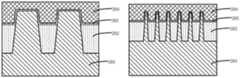
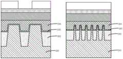
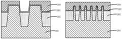
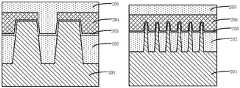
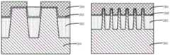
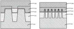
下面参考附图对本发明的半导体器件的制备方法做详细描述,图1示出了本发明所述半导体器件的制备工艺流程图;图2示出了本发明所述半导体器件的制备方法实施所获得结构的剖面示意图;图3示出了本发明所述半导体器件的制备方法实施所获得结构的剖面示意图;图4示出了本发明所述半导体器件的制备方法实施所获得结构的剖面示意图;图5示出了本发明所述半导体器件的制备方法实施所获得结构的剖面示意图;图6示出了本发明所述半导体器件的制备方法实施所获得结构的剖面示意图;图7示出了本发明所述半导体器件的制备方法实施所获得结构的剖面示意图;图8示出了本发明所述半导体器件的制备方法实施所获得结构的剖面示意图;图9示出了本发明所述半导体器件的制备方法实施所获得结构的剖面示意图;图10示出了本发明所述半导体器件的制备方法实施所获得结构的剖面示意图;图11示出了本发明所述半导体器件的制备方法实施所获得结构的剖面示意图。其中在图2至图11中左侧的示意图为沿鳍片结构延伸方向的剖面示意图,右侧的示意图为沿与鳍片结构延伸方向垂直的方向的剖面示意图。The manufacturing method of the semiconductor device of the present invention will be described in detail below with reference to the accompanying drawings. FIG. 1 shows a flow chart of the manufacturing process of the semiconductor device of the present invention; Schematic cross-sectional view of the structure; FIG. 3 shows a schematic cross-sectional view of the structure obtained by implementing the method for manufacturing a semiconductor device of the present invention; FIG. 4 shows a schematic cross-sectional view of the structure obtained by implementing the manufacturing method for a semiconductor device according to the present invention; 5 shows a schematic cross-sectional view of the structure obtained by the method for manufacturing a semiconductor device of the present invention; FIG. 6 shows a schematic cross-sectional view of the structure obtained by implementing the method for manufacturing a semiconductor device of the present invention; FIG. 7 shows the present invention The schematic cross-sectional view of the structure obtained by the method for manufacturing the semiconductor device; FIG. 8 shows the schematic cross-sectional view of the structure obtained by the method for manufacturing the semiconductor device of the present invention; FIG. 9 shows the preparation of the semiconductor device of the present invention A schematic cross-sectional view of a structure obtained by implementing the method; FIG. 10 shows a schematic cross-sectional view of a structure obtained by implementing the method for manufacturing a semiconductor device according to the present invention; FIG. Schematic cross section. The schematic diagrams on the left side in FIGS. 2 to 11 are schematic cross-sectional views along the extending direction of the fin structure, and the schematic diagrams on the right side are schematic cross-sectional views along the direction perpendicular to the extending direction of the fin structure.
本发明提供一种半导体器件的制备方法,如图1所示,该制备方法的主要步骤包括:The present invention provides a preparation method of a semiconductor device, as shown in FIG. 1 , the main steps of the preparation method include:
步骤S1:提供半导体衬底,在所述半导体衬底上形成有多列条状鳍片;Step S1: providing a semiconductor substrate, and forming a plurality of rows of strip-shaped fins on the semiconductor substrate;
步骤S2:图案化所述条状鳍片,以在所述条状鳍片中形成凹槽并在所述条状鳍片的延伸方向上将所述条状鳍片分割为相互间隔的鳍片结构;Step S2: Patterning the strip fins to form grooves in the strip fins and dividing the strip fins into spaced fins in the extending direction of the strip fins structure;
步骤S3:形成第一隔离材料层至所述鳍片结构的顶部以下,以露出所述鳍片结构的顶部;Step S3: forming a first isolation material layer below the top of the fin structure to expose the top of the fin structure;
步骤S4:在露出的所述鳍片结构上形成第一栅极材料层,以填充所述凹槽和所述鳍片结构之间的间隙并覆盖所述鳍片结构;Step S4: forming a first gate material layer on the exposed fin structure to fill the gap between the groove and the fin structure and cover the fin structure;
步骤S5:去除所述凹槽中的所述第一栅极材料层;Step S5: removing the first gate material layer in the groove;
步骤S6:沉积第二隔离材料层,以填充去除所述第一栅极材料层之后的所述凹槽。Step S6 : depositing a second isolation material layer to fill the groove after removing the first gate material layer.
下面,对本发明的半导体器件的制备方法的具体实施方式做详细的说明。Hereinafter, specific embodiments of the manufacturing method of the semiconductor device of the present invention will be described in detail.
首先,执行步骤一,提供半导体衬底201,在所述半导体衬底上形成有若干条状鳍片。First, step 1 is performed to provide a
具体地,如图2所示,在该步骤中所述半导体衬底可以是以下所提到的材料中的至少一种:硅、绝缘体上硅(SOI)、绝缘体上层叠硅(SSOI)、绝缘体上层叠锗化硅(S-SiGeOI)、绝缘体上锗化硅(SiGeOI)以及绝缘体上锗(GeOI)等。Specifically, as shown in FIG. 2 , in this step, the semiconductor substrate may be at least one of the following materials: silicon, silicon-on-insulator (SOI), stacked silicon-on-insulator (SSOI), insulator Silicon germanium (S-SiGeOI), silicon germanium on insulator (SiGeOI) and germanium on insulator (GeOI) are stacked on top.
在该实施例中半导体衬底201选用硅。In this embodiment, the
接着在所述半导体衬底上形成垫氧化物层(Pad oxide),其中所述垫氧化物层(Pad oxide)的形成方法可以通过沉积的方法形成,例如化学气相沉积、原子层沉积等方法,还可以通过热氧化所述半导体衬底的表面形成,在此不再赘述。Next, a pad oxide layer (Pad oxide) is formed on the semiconductor substrate, wherein the formation method of the pad oxide layer (Pad oxide) can be formed by a deposition method, such as chemical vapor deposition, atomic layer deposition and other methods, It can also be formed by thermally oxidizing the surface of the semiconductor substrate, which is not repeated here.
进一步,在该步骤中还可以进一步包含执行离子注入的步骤,以在所述半导体衬底中形成阱,其中注入的离子种类以及注入方法可以为本领域中常用的方法,在此不一一赘述。Further, this step may further include a step of performing ion implantation to form a well in the semiconductor substrate, wherein the implanted ion species and the implantation method may be methods commonly used in the field, and will not be described here. .
然后,在半导体衬底上形成若干相互平行的条状鳍片,例如所述条状鳍片包括若干列,以形成鳍片阵列。Then, several mutually parallel strip-shaped fins are formed on the semiconductor substrate, for example, the strip-shaped fins include several columns to form a fin array.
其中,鳍片的宽度全部相同,或者鳍片分为具有不同宽度的多个鳍片组。Wherein, the widths of the fins are all the same, or the fins are divided into multiple fin groups with different widths.
在所述垫氧化物层上形成硬掩膜层。A hard mask layer is formed on the pad oxide layer.
具体地,如图2所示,其中,所述垫氧化物层作为所述硬掩膜层的缓冲层,所述垫氧化物层可以解决在隔离材料层回蚀刻过程中硬掩膜层SiN脱落的问题。Specifically, as shown in FIG. 2 , wherein the pad oxide layer serves as a buffer layer of the hard mask layer, and the pad oxide layer can solve the problem that the SiN of the hard mask layer falls off during the etching back process of the isolation material layer. The problem.
其中,所述硬掩膜层选用SiN。Wherein, SiN is selected for the hard mask layer.
图案化所垫氧化物层、硬掩膜层和所述半导体衬底,以形成若干条状鳍片。The pad oxide layer, the hard mask layer, and the semiconductor substrate are patterned to form strip-shaped fins.
具体的形成方法包括:在半导体衬底上形成光刻胶层(图中未示出),形成所述光刻胶层可以采用本领域技术人员所熟习的各种适宜的工艺,图案化所述光刻胶层,形成用于蚀刻半导体衬底以在其上形成鳍片的多个彼此隔离的掩膜,然后以所述光刻胶层为掩膜蚀刻所述垫氧化物层、硬掩膜层和所述半导体衬底,以形成多列所述条状鳍片。The specific forming method includes: forming a photoresist layer (not shown in the figure) on a semiconductor substrate, and forming the photoresist layer can adopt various suitable processes familiar to those skilled in the art, patterning the photoresist layer A photoresist layer, forming a plurality of isolated masks for etching the semiconductor substrate to form fins thereon, and then using the photoresist layer as a mask to etch the pad oxide layer, hard mask layer and the semiconductor substrate to form a plurality of rows of the strip-shaped fins.
接着形成衬垫氧化物层,以覆盖半导体衬底的表面、鳍片结构的侧壁以及所述硬掩膜层的侧壁和顶部。A pad oxide layer is then formed to cover the surface of the semiconductor substrate, the sidewalls of the fin structure, and the sidewalls and top of the hard mask layer.
在一个实施例中,采用现场蒸汽生成工艺(ISSG)形成衬垫氧化物层。In one embodiment, the pad oxide layer is formed using an in-situ steam generation process (ISSG).
可选地,在该步骤中还可以形成覆盖衬垫氧化物层的保护层,以避免后续实施的工艺对鳍片结构的高度和特征尺寸造成损失。在一个实施例中,采用具有可流动性的化学气相沉积工艺(FCVD)形成保护层,保护层的材料可以为氮化硅。Optionally, in this step, a protective layer covering the pad oxide layer may also be formed, so as to avoid the loss of the height and feature size of the fin structure in the subsequent process. In one embodiment, a flowable chemical vapor deposition process (FCVD) is used to form the protective layer, and the material of the protective layer may be silicon nitride.
图案化所述条状鳍片,以在所述条状鳍片上形成若干凹槽,以在所述条状鳍片的延伸方向上形成若干相互间隔的鳍片结构;patterning the strip-shaped fins to form a plurality of grooves on the strip-shaped fins, so as to form a plurality of mutually spaced fin structures in the extending direction of the strip-shaped fins;
执行步骤二,图案化所述条状鳍片,以在所述条状鳍片上形成凹槽,在所述条状鳍片的延伸方向上形成相互间隔的鳍片结构。Step 2 is performed, the strip-shaped fins are patterned to form grooves on the strip-shaped fins, and fin structures spaced apart from each other are formed in the extending direction of the strip-shaped fins.
具体地,如图2所示,在所述条状鳍片的延伸方向上对所述条状鳍片进行图案化,以将所述条状鳍片在其延伸方向上被分割为若干相互间隔的部分。Specifically, as shown in FIG. 2 , the strip-shaped fins are patterned in the extending direction of the strip-shaped fins, so that the strip-shaped fins are divided into several intervals in the extending direction thereof. part.
具体地,在所述条状鳍片上形成若干凹槽,在所述条状鳍片的延伸方向上形成若干相互间隔的鳍片结构。Specifically, several grooves are formed on the strip-shaped fins, and several mutually spaced fin structures are formed in the extending direction of the strip-shaped fins.
执行步骤三,沉积第一隔离材料层202,以填充所述凹槽并覆盖所述鳍片结构。Step 3 is performed to deposit a first
具体地,如图2所示,沉积第一隔离材料层,以完全填充鳍片结构之间的间隙,例如填充相邻两列鳍片结构之间的间隙。Specifically, as shown in FIG. 2 , a first isolation material layer is deposited to completely fill the gaps between the fin structures, for example, to fill the gaps between two adjacent columns of fin structures.
在一个实施例中,采用具有可流动性的化学气相沉积工艺实施所述沉积。隔离材料层的材料可以选择氧化物,例如HARP。In one embodiment, the deposition is performed using a flowable chemical vapor deposition process. The material of the isolation material layer can be selected from oxide, such as HARP.
在沉积所述隔离材料层之后还进一步包括平坦化的步骤,例如平坦化所述第一隔离材料层至所述鳍片结构顶部的步骤。After depositing the isolation material layer, a planarization step is further included, for example, a step of planarizing the first isolation material layer to the top of the fin structure.
执行步骤四,回蚀刻所述第一隔离材料层202,以去除部分所述第一隔离材料层并露出所述鳍片结构的顶部。Step 4 is performed to etch back the first
具体地,如图3所示,在该步骤中回蚀刻所述第一隔离材料层202,以露出所述鳍片结构顶部,从而形成目标高度的鳍片结构。Specifically, as shown in FIG. 3 , in this step, the first
其中,所述目标高度是指在器件设计中所需要形成的高度,并不局限于某一数值范围。The target height refers to the height that needs to be formed in the device design, and is not limited to a certain numerical range.
其中,所述第一隔离材料层选用氧化物。Wherein, oxide is selected for the first isolation material layer.
在该步骤中选用远程等离子体反应(Siconi制程,Remote plasma reaction)或者气体蚀刻方法(例如Certas制程)回蚀刻所述第一隔离材料层。其中,所述Siconi制程和所述Certas制程的各种操作方法和参数均可以参照本领域中常规的Siconi制程和所述Certas制程,在此不再赘述。In this step, a remote plasma reaction (Siconi process, Remote plasma reaction) or a gas etching method (eg Certas process) is used to etch back the first isolation material layer. Wherein, the various operation methods and parameters of the Siconi process and the Certas process can refer to the conventional Siconi process and the Certas process in the art, which will not be repeated here.
执行步骤五,在露出的所述鳍片结构和所述第一隔离材料层上形成栅极介电层203。Step 5 is performed to form a
具体地,如图3所示,在露出的所述鳍片结构和所述第一隔离材料层上形成栅极介电层,以覆盖所述鳍片结构。Specifically, as shown in FIG. 3 , a gate dielectric layer is formed on the exposed fin structure and the first isolation material layer to cover the fin structure.
其中,所述栅极介电层可以通过热氧化的方法或者沉积的方法形成。所述栅极介电层203选用氧化物。Wherein, the gate dielectric layer may be formed by a thermal oxidation method or a deposition method. The
所述栅极介电层的厚度并不局限于某一数值范围。The thickness of the gate dielectric layer is not limited to a certain value range.
执行步骤六,在所述栅极介电层上形成第一栅极材料层204,以填充回蚀刻之后的所述凹槽和所述鳍片结构之间的间隙并覆盖所述鳍片结构。Step 6 is performed to form a first
具体地,如图5所示,其中,所述第一栅极材料层作为缓冲层填充所述鳍片结构之间的间隙,包括不同列所述鳍片结构之间的间隙以及同列的所述鳍片结构中间的凹槽。Specifically, as shown in FIG. 5 , wherein the first gate material layer acts as a buffer layer to fill the gaps between the fin structures, including the gaps between the fin structures in different columns and the gaps between the fin structures in the same column The groove in the middle of the fin structure.
其中,所述第一栅极材料层选用与所述第一隔离材料层具有较大蚀刻选择比的材料,以防止其被损坏。Wherein, the first gate material layer is selected from a material with a larger etching selectivity ratio than the first isolation material layer to prevent it from being damaged.
可选地,所述第一栅极材料层还用于后续形成栅极结构的材料,因此所述第一栅极材料层选用多晶硅。Optionally, the first gate material layer is also used as a material for the subsequent formation of the gate structure, so polysilicon is selected for the first gate material layer.
执行步骤七,图案化所述第一栅极材料层,以去除所述凹槽中的所述第一栅极材料层。Step 7 is performed to pattern the first gate material layer to remove the first gate material layer in the groove.
具体地,如图6所示,图案化所述第一栅极材料层,以去除所述凹槽中的所述第一栅极材料层的步骤包括:Specifically, as shown in FIG. 6 , the step of patterning the first gate material layer to remove the first gate material layer in the groove includes:
步骤1:在所述第一栅极材料层上形成掩膜叠层,所述掩膜叠层中形成有与所述凹槽对准的开口图案;Step 1: forming a mask stack on the first gate material layer, and an opening pattern aligned with the groove is formed in the mask stack;
步骤2:以所述掩膜叠层为掩膜蚀刻所述凹槽中的第一栅极材料层,以露出所述凹槽中的所述第一隔离材料层。Step 2: etching the first gate material layer in the groove by using the mask stack as a mask to expose the first isolation material layer in the groove.
在所述步骤1中,所述掩膜叠层包括依次沉积的ODL层、Si-BARC层以及图案化的光刻胶层。有机分布层(Organic distribution layer,ODL),含硅的底部抗反射涂层(Si-BARC),在所述含硅的底部抗反射涂层(Si-BARC)上沉积图案化了的光刻胶层,其中所述光刻胶上的图案定义了所要形成开口的图形。In the step 1, the mask stack includes a sequentially deposited ODL layer, a Si-BARC layer, and a patterned photoresist layer. Organic distribution layer (ODL), silicon-containing bottom anti-reflective coating (Si-BARC) on which patterned photoresist is deposited layer, wherein the pattern on the photoresist defines the pattern of openings to be formed.
所述蚀刻步骤为干法蚀刻或者湿法蚀刻,以去除所述凹槽中的所述第一栅极材料层。The etching step is dry etching or wet etching to remove the first gate material layer in the groove.
在该步骤中为了提高蚀刻效率,选用与所述第一隔离材料层具有较大蚀刻选择比的蚀刻方法,例如使用HBr基蚀刻气体来蚀刻所述第一栅极材料层,如图7所示。In this step, in order to improve the etching efficiency, an etching method with a larger etching selectivity ratio to the first isolation material layer is selected, for example, an HBr-based etching gas is used to etch the first gate material layer, as shown in FIG. 7 . .
执行步骤八,沉积第二隔离材料层205,以填充去除所述第一栅极材料层之后的所述凹槽。Step 8 is performed to deposit a second
其中,沉积第二隔离材料层,以填充去除所述第一栅极材料层之后的所述凹槽的步骤包括:Wherein, the step of depositing a second isolation material layer to fill the groove after removing the first gate material layer includes:
步骤1:沉积第二隔离材料层,以填充去除所述第一栅极材料层之后的所述凹槽并覆盖所述第一栅极材料层,如图8所示。Step 1: depositing a second isolation material layer to fill the groove after removing the first gate material layer and cover the first gate material layer, as shown in FIG. 8 .
步骤2:回蚀刻所述第二隔离材料层,以去除所述第一栅极材料层表面的所述第二隔离材料层,并将所述凹槽中的所述第二隔离材料层蚀刻至所述第一栅极材料层以下,如图9所示。Step 2: etch back the second isolation material layer to remove the second isolation material layer on the surface of the first gate material layer, and etch the second isolation material layer in the groove to Below the first gate material layer, as shown in FIG. 9 .
在所述步骤1中,如图8所示,在该步骤中沉积第二隔离材料层205至所述第一栅极材料层顶部以上,以填充去除所述第一栅极材料层之后的所述凹槽。In the step 1, as shown in FIG. 8, a second
其中,所述第二隔离材料层205选用流动式化学气相沉积法(Flowable CVD:FCVD)的方法沉积。Wherein, the second
可选地,所述第二隔离材料层选用氧化物。Optionally, oxide is selected for the second isolation material layer.
在所述步骤2中,选用远程等离子体反应(Siconi制程,Remote plasma reaction)或者气体蚀刻方法(例如Certas制程)回蚀刻所述第二隔离材料层。其中,所述Siconi制程和所述Certas制程的各种操作方法和参数均可以参照本领域中常规的Siconi制程和所述Certas制程,在此不再赘述。In the step 2, the second isolation material layer is etched back by selecting a remote plasma reaction (Siconi process, Remote plasma reaction) or a gas etching method (eg, Certas process). Wherein, the various operation methods and parameters of the Siconi process and the Certas process can refer to the conventional Siconi process and the Certas process in the art, which will not be repeated here.
执行步骤九,在所述第一栅极材料层和所述第二隔离材料层上形成第二栅极材料层206,以覆盖所述第一栅极材料层和所述第二隔离材料层。Step 9 is performed to form a second
具体地,如图10所示,所述第二栅极材料层206包括多晶硅。Specifically, as shown in FIG. 10 , the second
所述第二栅极材料层的沉积方法可以选用本领域常用的方法。The deposition method of the second gate material layer may be a method commonly used in the art.
在形成所述第二栅极材料层之后还进一步包括平坦化的步骤,所述平坦化处理的非限制性实例包括机械平坦化方法和化学机械抛光平坦化方法。After the formation of the second gate material layer, a planarization step is further included, and non-limiting examples of the planarization process include a mechanical planarization method and a chemical mechanical polishing planarization method.
执行步骤十,对所述第二栅极材料层和第一栅极材料层进行图案化,以分别在所述凹槽上方、所述鳍片结构上方形成栅极结构。Step 10 is performed to pattern the second gate material layer and the first gate material layer to form a gate structure on the groove and the fin structure, respectively.
具体地,如图11所示,在该步骤中图案化所述第一栅极材料层和所述第二栅极材料层,以形成环绕所述鳍片结构的栅极结构,例如所述栅极结构覆盖所述鳍片结构的顶部以及顶部两侧的两个侧壁,从而使所述栅极结构环绕所述鳍片结构设置,其中,位于所述凹槽上方的为虚拟栅极结构。Specifically, as shown in FIG. 11 , in this step, the first gate material layer and the second gate material layer are patterned to form a gate structure surrounding the fin structure, such as the gate The pole structure covers the top of the fin structure and two sidewalls on both sides of the top, so that the gate structure is disposed around the fin structure, wherein the dummy gate structure is located above the groove.
在该实施例中对所述凹槽上方的第二栅极材料层进行图案化,同时对所述鳍片结构上的述第二栅极材料层和第一栅极材料层进行图案化,以分别在所述凹槽上方、所述鳍片结构上方形成栅极结构,所述鳍片结构上方的栅极结构包括堆叠设置的图案化的第一栅极材料层和图案化的第二栅极材料层,所述凹槽上方的所述栅极结构仅包括图案化的第二栅极材料层。In this embodiment, the second gate material layer above the groove is patterned, and the second gate material layer and the first gate material layer on the fin structure are patterned at the same time, so as to A gate structure is formed over the groove and over the fin structure, respectively, and the gate structure over the fin structure includes a patterned first gate material layer and a patterned second gate arranged in a stack. A material layer, the gate structure above the groove includes only a patterned second gate material layer.
具体地,在所述第二栅极材料层上形成光刻胶层207,然后曝光显影,以形成开口,然后以所述光刻胶层207为掩膜蚀刻所述第一栅极材料层和所述第二栅极材料层,以形成环绕所述鳍片结构的栅极结构。Specifically, a
然后在所述栅极结构的侧壁上形成间隙壁并执行LDD离子注入。Spacers are then formed on the sidewalls of the gate structure and LDD ion implantation is performed.
所述偏移侧墙的材料例如是氮化硅,氧化硅或者氮氧化硅等绝缘材料。随着器件尺寸的进一步变小,器件的沟道长度越来越小,源漏极的粒子注入深度也越来越小,偏移侧墙的作用在于以提高形成的晶体管的沟道长度,减小短沟道效应和由于短沟道效应引起的热载流子效应。The material of the offset spacers is, for example, an insulating material such as silicon nitride, silicon oxide or silicon oxynitride. As the size of the device becomes smaller, the channel length of the device becomes smaller and smaller, and the particle implantation depth of the source and drain becomes smaller and smaller. The function of the offset sidewall is to increase the channel length of the formed transistor and reduce the Small short channel effect and hot carrier effect due to short channel effect.
其中,形成偏移侧墙的工艺可以为化学气相沉积,本实施例中,所述偏移侧墙的厚度可以小到80埃。The process for forming the offset sidewall spacer may be chemical vapor deposition, and in this embodiment, the thickness of the offset sidewall spacer may be as small as 80 angstroms.
可选地,在所述虚拟栅极两侧执行LDD离子注入步骤并活化。Optionally, an LDD ion implantation step and activation are performed on both sides of the dummy gate.
可选地,在所述虚拟栅极的偏移侧墙上形成间隙壁。Optionally, spacers are formed on the offset sidewalls of the dummy gate.
具体地,在所形成的偏移侧墙上形成间隙壁(Spacer),所述间隙壁可以为氧化硅、氮化硅、氮氧化硅中一种或者它们组合构成。作为本实施例的一中实施方式,所述间隙壁为氧化硅、氮化硅共同组成,具体工艺为:在半导体衬底上形成第一氧化硅层、第一氮化硅层以及第二氧化硅层,然后采用蚀刻方法形成间隙壁。Specifically, a spacer (Spacer) is formed on the formed offset sidewall, and the spacer may be one of silicon oxide, silicon nitride, silicon oxynitride, or a combination thereof. As an implementation manner of this embodiment, the spacers are composed of silicon oxide and silicon nitride, and the specific process is: forming a first silicon oxide layer, a first silicon nitride layer and a second oxide layer on a semiconductor substrate The silicon layer is then etched to form spacers.
此外,所述方法还进一步包括形成接触孔蚀刻停止层的步骤,所述形成方法可以选用本领域常用的各种方法,在此不再赘述。In addition, the method further includes the step of forming an etch stop layer for the contact hole, and the forming method can be selected from various methods commonly used in the art, which will not be repeated here.
至此,完成了本发明实施例的半导体器件制备的相关步骤的介绍。在上述步骤之后,还可以包括其他相关步骤,此处不再赘述。并且,除了上述步骤之外,本实施例的制备方法还可以在上述各个步骤之中或不同的步骤之间包括其他步骤,这些步骤均可以通过现有技术中的各种工艺来实现,此处不再赘述。So far, the introduction of the steps related to the fabrication of the semiconductor device according to the embodiment of the present invention is completed. After the above steps, other related steps may also be included, which will not be repeated here. Moreover, in addition to the above steps, the preparation method of this embodiment may also include other steps among the above steps or between different steps, and these steps can be realized by various processes in the prior art, here No longer.
为了解决目前工艺中存在的上述问题,本发明提供了一种半导体器件的制备方法,在所述方法中在形成所述目标高度的鳍片结构之后,在所述鳍片结构之间形成第一栅极材料层作为缓冲层,以填充所述鳍片结构之间的间隙,然后去除凹槽内的第一栅极材料层再沉积第二隔离材料层以作为单扩散区切断(single diffusion break,SDB),通过所述工艺的改进,可以避免目前工艺中所述单扩散区切断(single diffusion break,SDB)的横向(指沿鳍片结构的延伸方向)蚀刻,避免单扩散区切断(single diffusion break,SDB)横向厚度很小的问题,通过所述方法提高了所述半导体器件的性能和良率。In order to solve the above problems existing in the current process, the present invention provides a method for fabricating a semiconductor device. In the method, after the fin structures of the target height are formed, a first The gate material layer is used as a buffer layer to fill the gap between the fin structures, and then the first gate material layer in the groove is removed and a second isolation material layer is deposited to serve as a single diffusion break (single diffusion break, SDB), through the improvement of the process, the lateral (referring to the extension direction of the fin structure) etching of the single diffusion break (SDB) in the current process can be avoided, and the single diffusion break (single diffusion break) can be avoided. break, SDB) with a small lateral thickness, the performance and yield of the semiconductor device are improved by the method.
实施例二Embodiment 2
本发明还提供了一种半导体器件,如图11所示,所述半导体器件包括:The present invention also provides a semiconductor device, as shown in FIG. 11 , the semiconductor device includes:
半导体衬底201,所述半导体衬底上形成有多列条状鳍片,所述条状鳍片中形成有凹槽,所述凹槽在所述条状鳍片的延伸方向上将所述条状鳍片分割为相互间隔的鳍片结构;A
隔离材料层202,填充于所述凹槽中,所述隔离结构在所述延伸方向上的厚度均一。The
其中,所述隔离材料层202还填充所述相邻两列的所述鳍片结构之间的间隙。Wherein, the
所述半导体器件还包括:The semiconductor device further includes:
位于所述鳍片结构上方的栅极结构,包括堆叠设置的图案化的第一栅极材料层和图案化的第二栅极材料层;The gate structure above the fin structure includes a patterned first gate material layer and a patterned second gate material layer arranged in stacks;
位于所述凹槽上方的栅极结构,包括图案化的第二栅极材料层。The gate structure above the groove includes a patterned second gate material layer.
同样,所述栅极结构还填充所述相邻两列的所述鳍片结构之间的间隙,在与所述鳍片结构延伸方向垂直的方向上形成一体的栅极结构。Likewise, the gate structure also fills the gap between the fin structures of the two adjacent columns, forming an integrated gate structure in a direction perpendicular to the extending direction of the fin structures.
其中,所述半导体器件包括半导体衬底201,所述半导体衬底可以是以下所提到的材料中的至少一种:硅、绝缘体上硅(SOI)、绝缘体上层叠硅(SSOI)、绝缘体上层叠锗化硅(S-SiGeOI)、绝缘体上锗化硅(SiGeOI)以及绝缘体上锗(GeOI)等。在该实施例中半导体衬底选用硅。The semiconductor device includes a
具体地,在半导体衬底上形成有多个鳍片结构,鳍片结构的宽度全部相同,或者鳍片分为具有不同宽度的多个鳍片组。Specifically, a plurality of fin structures are formed on the semiconductor substrate, and the widths of the fin structures are all the same, or the fins are divided into a plurality of fin groups with different widths.
所述半导体器件还进一步包括环绕所述鳍片设置的栅极结构,所述栅结构的侧壁上形成有偏移侧壁和间隙壁。例如所述栅极结构覆盖所述鳍片结构的顶部以及顶部两侧的两个侧壁,从而使所述栅极结构环绕所述鳍片结构设置。The semiconductor device further includes a gate structure disposed around the fin, and offset sidewalls and spacers are formed on sidewalls of the gate structure. For example, the gate structure covers the top of the fin structure and two sidewalls on both sides of the top, so that the gate structure is disposed around the fin structure.
所述偏移侧墙的材料例如是氮化硅,氧化硅或者氮氧化硅等绝缘材料。随着器件尺寸的进一步变小,器件的沟道长度越来越小,源漏极的粒子注入深度也越来越小,偏移侧墙的作用在于以提高形成的晶体管的沟道长度,减小短沟道效应和由于短沟道效应引起的热载流子效应。The material of the offset spacers is, for example, an insulating material such as silicon nitride, silicon oxide or silicon oxynitride. As the size of the device becomes smaller, the channel length of the device becomes smaller and smaller, and the particle implantation depth of the source and drain becomes smaller and smaller. The function of the offset sidewall is to increase the channel length of the formed transistor and reduce the Small short channel effects and hot carrier effects due to short channel effects.
在所形成的偏移侧墙上形成有间隙壁(Spacer),所述间隙壁可以为氧化硅、氮化硅、氮氧化硅中一种或者它们组合构成。A spacer (spacer) is formed on the formed offset sidewall, and the spacer may be one of silicon oxide, silicon nitride, silicon oxynitride, or a combination thereof.
在所述栅极结构的两侧形成有抬升源漏。A raised source and drain are formed on both sides of the gate structure.
为了解决目前工艺中存在的上述问题,本发明提供了一种半导体器件,所述半导体器件在制备过程中在形成所述目标高度的鳍片结构之后,在所述鳍片结构之间形成第一栅极材料层作为缓冲层,以填充所述鳍片结构之间的间隙,然后去除凹槽内的第一栅极材料层再沉积第二隔离材料层以作为单扩散区切断(single diffusion break,SDB),通过所述工艺的改进,可以避免目前工艺中所述单扩散区切断(single diffusion break,SDB)的横向(指沿鳍片结构的延伸方向)蚀刻,避免单扩散区切断(single diffusion break,SDB)横向厚度很小的问题,通过所述方法提高了所述半导体器件的性能和良率。In order to solve the above-mentioned problems existing in the current process, the present invention provides a semiconductor device. After the fin structures of the target height are formed during the manufacturing process of the semiconductor device, a first fin structure is formed between the fin structures. The gate material layer is used as a buffer layer to fill the gap between the fin structures, and then the first gate material layer in the groove is removed and a second isolation material layer is deposited to serve as a single diffusion break (single diffusion break, SDB), through the improvement of the process, the lateral (referring to the extension direction of the fin structure) etching of the single diffusion break (SDB) in the current process can be avoided, and the single diffusion break (single diffusion break) can be avoided. break, SDB) lateral thickness is small, the performance and yield of the semiconductor device are improved by the method.
本发明的半导体器件,由于采用了上述制造方法,因而同样具有上述优点。Since the semiconductor device of the present invention adopts the above-mentioned manufacturing method, it also has the above-mentioned advantages.
实施例三Embodiment 3
本发明的另一个实施例提供一种电子装置,其包括半导体器件,该半导体器件为前述实施例二中的半导体器件,或根据实施例一所述的半导体器件的制备方法所制得的半导体器件。Another embodiment of the present invention provides an electronic device, which includes a semiconductor device, the semiconductor device is the semiconductor device in the foregoing second embodiment, or a semiconductor device prepared according to the method for manufacturing a semiconductor device in the first embodiment .
该电子装置,可以是手机、平板电脑、笔记本电脑、上网本、游戏机、电视机、VCD、DVD、导航仪、照相机、摄像机、录音笔、MP3、MP4、PSP等任何电子产品或设备,也可以是具有上述半导体器件的中间产品,例如:具有该集成电路的手机主板等。The electronic device can be any electronic product or device such as a mobile phone, tablet computer, notebook computer, netbook, game console, TV, VCD, DVD, navigator, camera, video camera, voice recorder, MP3, MP4, PSP, etc. It is an intermediate product with the above semiconductor devices, such as a mobile phone motherboard with the integrated circuit.
由于包括的半导体器件件具有更高的性能,该电子装置同样具有上述优点。The electronic device also has the above-mentioned advantages due to the higher performance of the included semiconductor device.
其中,图12示出移动电话手机的示例。移动电话手机300被设置有包括在外壳301中的显示部分302、操作按钮303、外部连接端口304、扬声器305、话筒306等。Among them, FIG. 12 shows an example of a mobile phone handset. The
其中所述移动电话手机包括前述的半导体器件,或根据实施例一所述的半导体器件的制备方法所制得的半导体器件,所述半导体器件包半导体衬底,所述半导体衬底上形成有多列条状鳍片,所述条状鳍片中形成有凹槽,所述凹槽在所述条状鳍片的延伸方向上将所述条状鳍片分割为相互间隔的鳍片结构;隔离材料层,填充于所述凹槽中,所述隔离结构在所述延伸方向上的厚度均一。所述半导体器件在制备过程中在形成所述目标高度的鳍片结构之后,在所述鳍片结构之间形成第一栅极材料层作为缓冲层,以填充所述鳍片结构之间的间隙,然后去除凹槽内的第一栅极材料层再沉积第二隔离材料层以作为单扩散区切断(single diffusion break,SDB),通过所述工艺的改进,可以避免目前工艺中所述单扩散区切断(single diffusion break,SDB)的横向(指沿鳍片结构的延伸方向)蚀刻,避免单扩散区切断(single diffusion break,SDB)横向厚度很小的问题,通过所述方法提高了所述半导体器件的性能和良率。The mobile phone includes the aforementioned semiconductor device, or a semiconductor device obtained by the method for manufacturing a semiconductor device according to Embodiment 1, wherein the semiconductor device includes a semiconductor substrate on which a plurality of semiconductor devices are formed. A row of strip-shaped fins, wherein grooves are formed in the strip-shaped fins, and the grooves divide the strip-shaped fins into mutually spaced fin structures in the extending direction of the strip-shaped fins; isolation The material layer is filled in the groove, and the thickness of the isolation structure in the extending direction is uniform. After the fin structures of the target height are formed in the manufacturing process of the semiconductor device, a first gate material layer is formed between the fin structures as a buffer layer to fill the gaps between the fin structures , then remove the first gate material layer in the groove and deposit a second isolation material layer to serve as a single diffusion break (SDB). Through the improvement of the process, the single diffusion in the current process can be avoided The lateral (referring to the extending direction of the fin structure) etching of the region cut off (single diffusion break, SDB) avoids the problem of small lateral thickness of the single diffusion break (SDB), and the method improves the Performance and yield of semiconductor devices.
本发明已经通过上述实施例进行了说明,但应当理解的是,上述实施例只是用于举例和说明的目的,而非意在将本发明限制于所描述的实施例范围内。此外本领域技术人员可以理解的是,本发明并不局限于上述实施例,根据本发明的教导还可以做出更多种的变型和修改,这些变型和修改均落在本发明所要求保护的范围以内。本发明的保护范围由附属的权利要求书及其等效范围所界定。The present invention has been described by the above-mentioned embodiments, but it should be understood that the above-mentioned embodiments are only for the purpose of illustration and description, and are not intended to limit the present invention to the scope of the described embodiments. In addition, those skilled in the art can understand that the present invention is not limited to the above-mentioned embodiments, and more variations and modifications can also be made according to the teachings of the present invention, and these variations and modifications all fall within the protection claimed in the present invention. within the range. The protection scope of the present invention is defined by the appended claims and their equivalents.
Claims (12)
Priority Applications (1)
| Application Number | Priority Date | Filing Date | Title |
|---|---|---|---|
| CN201611064785.4ACN108122840B (en) | 2016-11-28 | 2016-11-28 | A kind of semiconductor device and preparation method, electronic device |
Applications Claiming Priority (1)
| Application Number | Priority Date | Filing Date | Title |
|---|---|---|---|
| CN201611064785.4ACN108122840B (en) | 2016-11-28 | 2016-11-28 | A kind of semiconductor device and preparation method, electronic device |
Publications (2)
| Publication Number | Publication Date |
|---|---|
| CN108122840A CN108122840A (en) | 2018-06-05 |
| CN108122840Btrue CN108122840B (en) | 2020-12-08 |
Family
ID=62224489
Family Applications (1)
| Application Number | Title | Priority Date | Filing Date |
|---|---|---|---|
| CN201611064785.4AActiveCN108122840B (en) | 2016-11-28 | 2016-11-28 | A kind of semiconductor device and preparation method, electronic device |
Country Status (1)
| Country | Link |
|---|---|
| CN (1) | CN108122840B (en) |
Families Citing this family (3)
| Publication number | Priority date | Publication date | Assignee | Title |
|---|---|---|---|---|
| CN108807267B (en)* | 2017-04-26 | 2020-12-08 | 中芯国际集成电路制造(上海)有限公司 | Semiconductor device and method of manufacturing the same |
| CN110867413A (en)* | 2019-11-19 | 2020-03-06 | 上海华力集成电路制造有限公司 | Forming method of single diffusion region cut off |
| CN113745109B (en)* | 2020-05-27 | 2024-08-16 | 广东汉岂工业技术研发有限公司 | A FinFET manufacturing method |
Citations (1)
| Publication number | Priority date | Publication date | Assignee | Title |
|---|---|---|---|---|
| CN104051270A (en)* | 2013-03-15 | 2014-09-17 | 三星电子株式会社 | Method of forming semiconductor structure and semiconductor device |
Family Cites Families (4)
| Publication number | Priority date | Publication date | Assignee | Title |
|---|---|---|---|---|
| CN103855093B (en)* | 2012-11-30 | 2016-07-06 | 中国科学院微电子研究所 | Semiconductor device and method for manufacturing the same |
| CN103943621B (en)* | 2013-01-22 | 2019-08-13 | 联华电子股份有限公司 | Shallow trench isolation structure and forming method thereof |
| CN105990151A (en)* | 2015-03-04 | 2016-10-05 | 中芯国际集成电路制造(上海)有限公司 | Semiconductor device and manufacturing method thereof, and electronic device |
| KR102342847B1 (en)* | 2015-04-17 | 2021-12-23 | 삼성전자주식회사 | Semiconductor device and manufacturing method of the same |
- 2016
- 2016-11-28CNCN201611064785.4Apatent/CN108122840B/enactiveActive
Patent Citations (1)
| Publication number | Priority date | Publication date | Assignee | Title |
|---|---|---|---|---|
| CN104051270A (en)* | 2013-03-15 | 2014-09-17 | 三星电子株式会社 | Method of forming semiconductor structure and semiconductor device |
Also Published As
| Publication number | Publication date |
|---|---|
| CN108122840A (en) | 2018-06-05 |
Similar Documents
| Publication | Publication Date | Title |
|---|---|---|
| CN106601678B (en) | A kind of semiconductor device and its preparation method, electronic device | |
| CN106601683B (en) | A kind of semiconductor device and its preparation method, electronic device | |
| CN106158831A (en) | A kind of semiconductor devices and preparation method thereof and electronic installation | |
| CN108122840B (en) | A kind of semiconductor device and preparation method, electronic device | |
| CN106601680B (en) | A kind of semiconductor device and its preparation method, electronic device | |
| CN110648916B (en) | Semiconductor device, manufacturing method thereof and electronic device | |
| CN106601685B (en) | A kind of semiconductor device and its preparation method, electronic device | |
| CN110400751B (en) | Semiconductor device, manufacturing method thereof and electronic device | |
| CN109686702B (en) | Semiconductor structure and forming method thereof | |
| CN106601688A (en) | Semiconductor device and manufacturing method thereof, and electronic device | |
| CN106601675B (en) | A kind of semiconductor device and its preparation method, electronic device | |
| CN107978563B (en) | Semiconductor device, preparation method and electronic device | |
| CN108735670A (en) | A kind of semiconductor devices and its manufacturing method and electronic device | |
| CN107799593B (en) | A vertical FinFET device, preparation method thereof, and electronic device | |
| CN106601687A (en) | Semiconductor device, the preparation method thereof and electronic device | |
| CN109309048B (en) | Semiconductor structure and method of forming the same | |
| CN106601741A (en) | Semiconductor device, preparation method thereof and electronic device | |
| CN106601686B (en) | A kind of semiconductor device and preparation method thereof, electronic device | |
| CN106952813B (en) | Semiconductor device, manufacturing method thereof and electronic device | |
| CN105097516A (en) | FinFET device, manufacturing method thereof and electronic device | |
| CN107689330B (en) | A kind of semiconductor device and preparation method, electronic device | |
| CN109087890A (en) | A kind of semiconductor devices and its manufacturing method, electronic device | |
| CN106910685A (en) | A kind of semiconductor devices and preparation method thereof, electronic installation | |
| CN105990151A (en) | Semiconductor device and manufacturing method thereof, and electronic device | |
| CN106910686B (en) | Semiconductor device, preparation method thereof and electronic device |
Legal Events
| Date | Code | Title | Description |
|---|---|---|---|
| PB01 | Publication | ||
| PB01 | Publication | ||
| SE01 | Entry into force of request for substantive examination | ||
| SE01 | Entry into force of request for substantive examination | ||
| GR01 | Patent grant | ||
| GR01 | Patent grant |