CN108122487B - Display panel and sensing display panel - Google Patents
Display panel and sensing display panelDownload PDFInfo
- Publication number
- CN108122487B CN108122487BCN201710929100.6ACN201710929100ACN108122487BCN 108122487 BCN108122487 BCN 108122487BCN 201710929100 ACN201710929100 ACN 201710929100ACN 108122487 BCN108122487 BCN 108122487B
- Authority
- CN
- China
- Prior art keywords
- sensing
- display panel
- display
- layer
- semi
- Prior art date
- Legal status (The legal status is an assumption and is not a legal conclusion. Google has not performed a legal analysis and makes no representation as to the accuracy of the status listed.)
- Active
Links
Images


Classifications
- G—PHYSICS
- G09—EDUCATION; CRYPTOGRAPHY; DISPLAY; ADVERTISING; SEALS
- G09F—DISPLAYING; ADVERTISING; SIGNS; LABELS OR NAME-PLATES; SEALS
- G09F9/00—Indicating arrangements for variable information in which the information is built-up on a support by selection or combination of individual elements
- G09F9/30—Indicating arrangements for variable information in which the information is built-up on a support by selection or combination of individual elements in which the desired character or characters are formed by combining individual elements
- G—PHYSICS
- G06—COMPUTING OR CALCULATING; COUNTING
- G06F—ELECTRIC DIGITAL DATA PROCESSING
- G06F3/00—Input arrangements for transferring data to be processed into a form capable of being handled by the computer; Output arrangements for transferring data from processing unit to output unit, e.g. interface arrangements
- G06F3/01—Input arrangements or combined input and output arrangements for interaction between user and computer
- G06F3/03—Arrangements for converting the position or the displacement of a member into a coded form
- G06F3/041—Digitisers, e.g. for touch screens or touch pads, characterised by the transducing means
- G06F3/044—Digitisers, e.g. for touch screens or touch pads, characterised by the transducing means by capacitive means
- G06F3/0446—Digitisers, e.g. for touch screens or touch pads, characterised by the transducing means by capacitive means using a grid-like structure of electrodes in at least two directions, e.g. using row and column electrodes
- G—PHYSICS
- G02—OPTICS
- G02F—OPTICAL DEVICES OR ARRANGEMENTS FOR THE CONTROL OF LIGHT BY MODIFICATION OF THE OPTICAL PROPERTIES OF THE MEDIA OF THE ELEMENTS INVOLVED THEREIN; NON-LINEAR OPTICS; FREQUENCY-CHANGING OF LIGHT; OPTICAL LOGIC ELEMENTS; OPTICAL ANALOGUE/DIGITAL CONVERTERS
- G02F1/00—Devices or arrangements for the control of the intensity, colour, phase, polarisation or direction of light arriving from an independent light source, e.g. switching, gating or modulating; Non-linear optics
- G02F1/01—Devices or arrangements for the control of the intensity, colour, phase, polarisation or direction of light arriving from an independent light source, e.g. switching, gating or modulating; Non-linear optics for the control of the intensity, phase, polarisation or colour
- G02F1/13—Devices or arrangements for the control of the intensity, colour, phase, polarisation or direction of light arriving from an independent light source, e.g. switching, gating or modulating; Non-linear optics for the control of the intensity, phase, polarisation or colour based on liquid crystals, e.g. single liquid crystal display cells
- G02F1/133—Constructional arrangements; Operation of liquid crystal cells; Circuit arrangements
- G02F1/1333—Constructional arrangements; Manufacturing methods
- G02F1/13338—Input devices, e.g. touch panels
- G—PHYSICS
- G02—OPTICS
- G02F—OPTICAL DEVICES OR ARRANGEMENTS FOR THE CONTROL OF LIGHT BY MODIFICATION OF THE OPTICAL PROPERTIES OF THE MEDIA OF THE ELEMENTS INVOLVED THEREIN; NON-LINEAR OPTICS; FREQUENCY-CHANGING OF LIGHT; OPTICAL LOGIC ELEMENTS; OPTICAL ANALOGUE/DIGITAL CONVERTERS
- G02F1/00—Devices or arrangements for the control of the intensity, colour, phase, polarisation or direction of light arriving from an independent light source, e.g. switching, gating or modulating; Non-linear optics
- G02F1/01—Devices or arrangements for the control of the intensity, colour, phase, polarisation or direction of light arriving from an independent light source, e.g. switching, gating or modulating; Non-linear optics for the control of the intensity, phase, polarisation or colour
- G02F1/13—Devices or arrangements for the control of the intensity, colour, phase, polarisation or direction of light arriving from an independent light source, e.g. switching, gating or modulating; Non-linear optics for the control of the intensity, phase, polarisation or colour based on liquid crystals, e.g. single liquid crystal display cells
- G02F1/133—Constructional arrangements; Operation of liquid crystal cells; Circuit arrangements
- G02F1/1333—Constructional arrangements; Manufacturing methods
- G02F1/1335—Structural association of cells with optical devices, e.g. polarisers or reflectors
- G02F1/133553—Reflecting elements
- G02F1/133555—Transflectors
- G—PHYSICS
- G02—OPTICS
- G02F—OPTICAL DEVICES OR ARRANGEMENTS FOR THE CONTROL OF LIGHT BY MODIFICATION OF THE OPTICAL PROPERTIES OF THE MEDIA OF THE ELEMENTS INVOLVED THEREIN; NON-LINEAR OPTICS; FREQUENCY-CHANGING OF LIGHT; OPTICAL LOGIC ELEMENTS; OPTICAL ANALOGUE/DIGITAL CONVERTERS
- G02F1/00—Devices or arrangements for the control of the intensity, colour, phase, polarisation or direction of light arriving from an independent light source, e.g. switching, gating or modulating; Non-linear optics
- G02F1/01—Devices or arrangements for the control of the intensity, colour, phase, polarisation or direction of light arriving from an independent light source, e.g. switching, gating or modulating; Non-linear optics for the control of the intensity, phase, polarisation or colour
- G02F1/23—Devices or arrangements for the control of the intensity, colour, phase, polarisation or direction of light arriving from an independent light source, e.g. switching, gating or modulating; Non-linear optics for the control of the intensity, phase, polarisation or colour for the control of the colour
- G—PHYSICS
- G06—COMPUTING OR CALCULATING; COUNTING
- G06F—ELECTRIC DIGITAL DATA PROCESSING
- G06F3/00—Input arrangements for transferring data to be processed into a form capable of being handled by the computer; Output arrangements for transferring data from processing unit to output unit, e.g. interface arrangements
- G06F3/01—Input arrangements or combined input and output arrangements for interaction between user and computer
- G06F3/03—Arrangements for converting the position or the displacement of a member into a coded form
- G06F3/041—Digitisers, e.g. for touch screens or touch pads, characterised by the transducing means
- G06F3/0412—Digitisers structurally integrated in a display
- G—PHYSICS
- G06—COMPUTING OR CALCULATING; COUNTING
- G06F—ELECTRIC DIGITAL DATA PROCESSING
- G06F3/00—Input arrangements for transferring data to be processed into a form capable of being handled by the computer; Output arrangements for transferring data from processing unit to output unit, e.g. interface arrangements
- G06F3/01—Input arrangements or combined input and output arrangements for interaction between user and computer
- G06F3/03—Arrangements for converting the position or the displacement of a member into a coded form
- G06F3/041—Digitisers, e.g. for touch screens or touch pads, characterised by the transducing means
- G06F3/042—Digitisers, e.g. for touch screens or touch pads, characterised by the transducing means by opto-electronic means
- G—PHYSICS
- G06—COMPUTING OR CALCULATING; COUNTING
- G06F—ELECTRIC DIGITAL DATA PROCESSING
- G06F3/00—Input arrangements for transferring data to be processed into a form capable of being handled by the computer; Output arrangements for transferring data from processing unit to output unit, e.g. interface arrangements
- G06F3/01—Input arrangements or combined input and output arrangements for interaction between user and computer
- G06F3/03—Arrangements for converting the position or the displacement of a member into a coded form
- G06F3/041—Digitisers, e.g. for touch screens or touch pads, characterised by the transducing means
- G06F3/044—Digitisers, e.g. for touch screens or touch pads, characterised by the transducing means by capacitive means
- G06F3/0443—Digitisers, e.g. for touch screens or touch pads, characterised by the transducing means by capacitive means using a single layer of sensing electrodes
- G—PHYSICS
- G09—EDUCATION; CRYPTOGRAPHY; DISPLAY; ADVERTISING; SEALS
- G09F—DISPLAYING; ADVERTISING; SIGNS; LABELS OR NAME-PLATES; SEALS
- G09F9/00—Indicating arrangements for variable information in which the information is built-up on a support by selection or combination of individual elements
- G09F9/30—Indicating arrangements for variable information in which the information is built-up on a support by selection or combination of individual elements in which the desired character or characters are formed by combining individual elements
- G09F9/301—Indicating arrangements for variable information in which the information is built-up on a support by selection or combination of individual elements in which the desired character or characters are formed by combining individual elements flexible foldable or roll-able electronic displays, e.g. thin LCD, OLED
- G—PHYSICS
- G02—OPTICS
- G02F—OPTICAL DEVICES OR ARRANGEMENTS FOR THE CONTROL OF LIGHT BY MODIFICATION OF THE OPTICAL PROPERTIES OF THE MEDIA OF THE ELEMENTS INVOLVED THEREIN; NON-LINEAR OPTICS; FREQUENCY-CHANGING OF LIGHT; OPTICAL LOGIC ELEMENTS; OPTICAL ANALOGUE/DIGITAL CONVERTERS
- G02F1/00—Devices or arrangements for the control of the intensity, colour, phase, polarisation or direction of light arriving from an independent light source, e.g. switching, gating or modulating; Non-linear optics
- G02F1/01—Devices or arrangements for the control of the intensity, colour, phase, polarisation or direction of light arriving from an independent light source, e.g. switching, gating or modulating; Non-linear optics for the control of the intensity, phase, polarisation or colour
- G02F1/13—Devices or arrangements for the control of the intensity, colour, phase, polarisation or direction of light arriving from an independent light source, e.g. switching, gating or modulating; Non-linear optics for the control of the intensity, phase, polarisation or colour based on liquid crystals, e.g. single liquid crystal display cells
- G02F1/133—Constructional arrangements; Operation of liquid crystal cells; Circuit arrangements
- G02F1/1333—Constructional arrangements; Manufacturing methods
- G02F1/1335—Structural association of cells with optical devices, e.g. polarisers or reflectors
- G02F1/133509—Filters, e.g. light shielding masks
- G02F1/133514—Colour filters
- G—PHYSICS
- G06—COMPUTING OR CALCULATING; COUNTING
- G06F—ELECTRIC DIGITAL DATA PROCESSING
- G06F2203/00—Indexing scheme relating to G06F3/00 - G06F3/048
- G06F2203/041—Indexing scheme relating to G06F3/041 - G06F3/045
- G06F2203/04103—Manufacturing, i.e. details related to manufacturing processes specially suited for touch sensitive devices
- G—PHYSICS
- G06—COMPUTING OR CALCULATING; COUNTING
- G06F—ELECTRIC DIGITAL DATA PROCESSING
- G06F2203/00—Indexing scheme relating to G06F3/00 - G06F3/048
- G06F2203/041—Indexing scheme relating to G06F3/041 - G06F3/045
- G06F2203/04111—Cross over in capacitive digitiser, i.e. details of structures for connecting electrodes of the sensing pattern where the connections cross each other, e.g. bridge structures comprising an insulating layer, or vias through substrate
Landscapes
- Engineering & Computer Science (AREA)
- Physics & Mathematics (AREA)
- Theoretical Computer Science (AREA)
- General Engineering & Computer Science (AREA)
- General Physics & Mathematics (AREA)
- Human Computer Interaction (AREA)
- Nonlinear Science (AREA)
- Optics & Photonics (AREA)
- Chemical & Material Sciences (AREA)
- Crystallography & Structural Chemistry (AREA)
- Mathematical Physics (AREA)
- Devices For Indicating Variable Information By Combining Individual Elements (AREA)
- Electroluminescent Light Sources (AREA)
Abstract
Translated fromChinese
Description
Translated fromChinese技术领域technical field
本发明涉及显示面板领域,特别涉及一种显示面板以及感测显示面板。The present invention relates to the field of display panels, in particular to a display panel and a sensing display panel.
背景技术Background technique
显示面板的色彩表现,通常是以美国国家电视系统委员会(National TelevisionSystem Committee;NTSC)所订定的标准来衡量显示面板的色彩饱和度。一般而言,为了提高显示面板的色彩饱和度,在现行的技术下可以在显示面板中采用高色彩饱和度的彩色滤光层。然而,高色彩饱和度的彩色滤光层的穿透率低,常需要通过提高显示元件的驱动功率以维持显示面板的发光亮度。若要提升显示面板的色彩饱和度则可能会面临功耗提升的问题。The color performance of the display panel is usually measured by the standard set by the National Television System Committee (NTSC) of the United States to measure the color saturation of the display panel. Generally speaking, in order to improve the color saturation of the display panel, a color filter layer with high color saturation can be used in the display panel under the current technology. However, the transmittance of the color filter layer with high color saturation is low, and it is often necessary to increase the driving power of the display element to maintain the luminous brightness of the display panel. If you want to increase the color saturation of the display panel, you may face the problem of increased power consumption.
除此之外,显示元件常需与感测元件搭配以构成感测显示面板,但具有感测元件搭配的感测显示面板可能会具有较低的开口率或透光率。如何进一步提升显示面板或感测显示面板的色彩饱和度,且提升显示面板或感测显示面板的开口率或透光率,实已成目前急需解决的课题。In addition, display elements often need to be matched with sensing elements to form a sensing display panel, but a sensing display panel with sensing elements may have a lower aperture ratio or transmittance. How to further improve the color saturation of the display panel or the sensing display panel, and improve the aperture ratio or light transmittance of the display panel or the sensing display panel, has become an urgent problem to be solved at present.
发明内容SUMMARY OF THE INVENTION
为了解决上述技术问题,本发明一目的在于提供一种显示面板和感测显示面板,其具有光学共振结构而可以提升显示面板或感测显示面板的色彩饱和度。In order to solve the above technical problems, an object of the present invention is to provide a display panel and a sensing display panel, which have an optical resonance structure and can improve the color saturation of the display panel or the sensing display panel.
具体地说,本发明一实施例公开了一种显示面板,其中包括:Specifically, an embodiment of the present invention discloses a display panel, which includes:
基板,具有布局区以及位于所述布局区以外的透光区;a substrate having a layout area and a light-transmitting area outside the layout area;
显示元件,配置于所述基板的所述布局区上,所述显示元件包括第一显示电极、第二显示电极以及位于所述第一显示电极与所述第二显示电极之间的显示介质层;A display element is disposed on the layout area of the substrate, and the display element includes a first display electrode, a second display electrode, and a display medium layer between the first display electrode and the second display electrode ;
介电层,位于所述基板上且覆盖所述显示元件;以及a dielectric layer on the substrate and covering the display element; and
光学共振结构,配置于所述介电层上且对应于所述显示元件分布,所述光学共振结构包括堆栈于所述显示元件上且彼此分离的第一半透层以及第二半透层。The optical resonance structure is disposed on the dielectric layer and corresponds to the distribution of the display element, and the optical resonance structure includes a first semi-transparent layer and a second semi-transparent layer stacked on the display element and separated from each other.
在一实施例中,所述显示面板,还包括感测元件,配置于所述封装层上且配置于所述基板的所述布局区上,所述感测元件包括相互电性绝缘的第一感测线路以及第二感测线路。In one embodiment, the display panel further includes a sensing element disposed on the packaging layer and on the layout area of the substrate, and the sensing element includes a first electrically insulated first. A sensing line and a second sensing line.
在一实施例中,所述显示面板,其中所述光学共振结构的所述第一半透层为一感测元件的一第一感测线路,而所述光学共振结构的所述第二半透层为所述感测元件的一第二感测线路。In one embodiment, the display panel, wherein the first semi-transparent layer of the optical resonance structure is a first sensing circuit of a sensing element, and the second semi-transparent layer of the optical resonance structure is The transparent layer is a second sensing circuit of the sensing element.
在一实施例中,所述显示面板,还包括位于所述第一半透层以及所述第二半透层之间的绝缘层。In one embodiment, the display panel further includes an insulating layer between the first semi-transparent layer and the second semi-transparent layer.
在一实施例中,所述显示面板,还包括第一感测线路,其中所述光学共振结构的所述第一半透层与所述第二半透层构成第二感测线路,且所述第一感测线路与所述第二感测线路构成感测元件。In one embodiment, the display panel further includes a first sensing circuit, wherein the first semi-transparent layer and the second semi-transparent layer of the optical resonance structure constitute a second sensing circuit, and the The first sensing circuit and the second sensing circuit constitute a sensing element.
在一实施例中,所述显示面板,还包括位于所述第一半透层以及所述第二半透层之间的透明导电层。In one embodiment, the display panel further includes a transparent conductive layer located between the first semi-transparent layer and the second semi-transparent layer.
在一实施例中,所述显示面板,还包括感测元件,其中所述感测元件包括多个感测线路、多个导电通孔以及至少一感测架桥,所述多个导电通孔位于所述多个感测线路与所述感测架桥之间,且部分的所述多个感测线路分别透过所述多个导电通孔与所述感测架桥电性连接。In one embodiment, the display panel further includes a sensing element, wherein the sensing element includes a plurality of sensing lines, a plurality of conductive vias and at least one sensing bridge, the plurality of conductive vias It is located between the plurality of sensing lines and the sensing bridge, and part of the plurality of sensing lines is electrically connected to the sensing bridge through the plurality of conductive vias respectively.
在一实施例中,所述显示面板,其中所述第一显示电极以及所述第二显示电极包括穿透电极。In one embodiment, the display panel, wherein the first display electrode and the second display electrode comprise penetration electrodes.
在一实施例中,所述显示面板,其中所述第二显示电极更配置于所述透光区。In one embodiment, in the display panel, the second display electrode is further disposed in the light-transmitting area.
在一实施例中,所述显示面板,其中所述显示面板还包括导光结构,配置于所述基板的所述透光区上。In one embodiment, the display panel, wherein the display panel further includes a light guide structure disposed on the light transmission area of the substrate.
本发明一实施例还提供一种感测显示面板,其中包括:An embodiment of the present invention also provides a sensing display panel, which includes:
基板,具有布局区以及位于所述布局区以外的透光区;a substrate having a layout area and a light-transmitting area outside the layout area;
显示元件,配置于所述基板的所述布局区上,所述显示元件包括第一显示电极、第二显示电极以及位于所述第一显示电极与所述第二显示电极之间的显示介质层;A display element is disposed on the layout area of the substrate, and the display element includes a first display electrode, a second display electrode, and a display medium layer between the first display electrode and the second display electrode ;
介电层,位于所述基板上且覆盖所述显示元件;以及a dielectric layer on the substrate and covering the display element; and
感测元件,配置于所述基板的所述布局区上且覆盖所述介电层,所述感测元件包括第一感测线路、第二感测线路以及位于所述第一感测线路与所述第二感测线路之间的绝缘层,其中所述第一感测线路以及所述第二感测线路包括半透电极,且所述第一感测线路以及所述第二感测线路堆栈于所述显示元件上以形成光学共振结构。A sensing element is disposed on the layout area of the substrate and covers the dielectric layer, and the sensing element includes a first sensing circuit, a second sensing circuit, and a first sensing circuit and a second sensing circuit. an insulating layer between the second sensing lines, wherein the first sensing lines and the second sensing lines comprise semi-transparent electrodes, and the first sensing lines and the second sensing lines stacked on the display element to form an optical resonance structure.
在一实施例中,所述感测显示面板,其中所述第一显示电极以及所述第二显示电极包括穿透电极。In one embodiment, the sensing display panel, wherein the first display electrode and the second display electrode comprise penetration electrodes.
在一实施例中,所述感测显示面板,其中所述第二显示电极更配置于所述透光区。In one embodiment, in the sensing display panel, the second display electrode is further disposed in the light-transmitting area.
在一实施例中,所述感测显示面板,其中所述感测显示面板还包括导光结构,配置于所述基板的所述透光区上。In one embodiment, the sensing display panel, wherein the sensing display panel further includes a light guide structure disposed on the light transmission area of the substrate.
本发明一实施例还提供一种感测显示面板,其中包括:An embodiment of the present invention also provides a sensing display panel, which includes:
基板,具有布局区以及位于所述布局区以外的透光区;a substrate having a layout area and a light-transmitting area outside the layout area;
显示元件,配置于所述基板的所述布局区上,所述显示元件包括第一显示电极、第二显示电极以及位于所述第一显示电极与所述第二显示电极之间的显示介质层;A display element is disposed on the layout area of the substrate, and the display element includes a first display electrode, a second display electrode, and a display medium layer between the first display electrode and the second display electrode ;
介电层,位于所述基板上且覆盖所述显示元件;以及a dielectric layer on the substrate and covering the display element; and
感测元件,配置于所述基板的所述布局区上且覆盖所述介电层,所述感测元件包括第一感测线路以及第二感测线路,其中所述第一感测线路包括半透电极,且所述第一感测线路包括堆栈于所述显示元件上以形成光学共振结构的第一感测部分以及第二感测部分。a sensing element, disposed on the layout area of the substrate and covering the dielectric layer, the sensing element includes a first sensing circuit and a second sensing circuit, wherein the first sensing circuit includes A semi-transparent electrode, and the first sensing circuit includes a first sensing portion and a second sensing portion stacked on the display element to form an optical resonance structure.
在一实施例中,所述感测显示面板,其中所述第一感测线路还包括配置于所述第一感测部分以及所述第二感测部分之间且堆栈于所述显示元件上的第一透明导电层。In one embodiment, the sensing display panel, wherein the first sensing circuit further comprises a configuration between the first sensing part and the second sensing part and stacked on the display element the first transparent conductive layer.
在一实施例中,所述感测显示面板,其中所述第二感测线路包括半透电极,且所述第二感测线路包括堆栈于所述显示元件上以形成光学共振结构的第三感测部分以及第四感测部分。In one embodiment, the sensing display panel, wherein the second sensing circuit includes a semi-transparent electrode, and the second sensing circuit includes a third layer stacked on the display element to form an optical resonance structure. a sensing part and a fourth sensing part.
在一实施例中,所述感测显示面板,其中所述第二感测线路还包括配置于所述第三感测部分以及所述第四感测部分之间且堆栈于所述显示元件上的第二透明导电层。In one embodiment, the sensing display panel, wherein the second sensing circuit further comprises a configuration between the third sensing part and the fourth sensing part and stacked on the display element the second transparent conductive layer.
在一实施例中,所述感测显示面板,其中所述第一显示电极以及所述第二显示电极包括穿透电极。In one embodiment, the sensing display panel, wherein the first display electrode and the second display electrode comprise penetration electrodes.
在一实施例中,所述感测显示面板,其中所述第二显示电极更配置于所述透光区。In one embodiment, in the sensing display panel, the second display electrode is further disposed in the light-transmitting area.
本发明一实施例的显示面板或感测显示面板具有光学共振结构,可以提升显示面板或感测显示面板的色彩饱和度。The display panel or the sensing display panel of an embodiment of the present invention has an optical resonance structure, which can improve the color saturation of the display panel or the sensing display panel.
附图说明Description of drawings
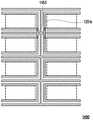
图1A为本发明第一实施例的显示面板的俯视示意图;1A is a schematic top view of a display panel according to a first embodiment of the present invention;
图1B为沿着图1A剖线AA’的剖面示意图;Fig. 1B is a schematic cross-sectional view along the section line AA' of Fig. 1A;
图2为本发明第二实施例的显示面板的剖面示意图;2 is a schematic cross-sectional view of a display panel according to a second embodiment of the present invention;
图3为本发明第三实施例的显示面板的剖面示意图;3 is a schematic cross-sectional view of a display panel according to a third embodiment of the present invention;
图4A为本发明第四实施例的显示面板的俯视示意图;4A is a schematic top view of a display panel according to a fourth embodiment of the present invention;
图4B为沿着图4A剖线BB’的剖面示意图;4B is a schematic cross-sectional view along the section line BB' of FIG. 4A;
图5A为本发明第五实施例的显示面板的俯视示意图;5A is a schematic top view of a display panel according to a fifth embodiment of the present invention;
图5B为沿着图5A剖线CC’的剖面示意图;FIG. 5B is a schematic cross-sectional view along the section line CC' of FIG. 5A;
图6为本发明第六实施例的显示面板的俯视示意图;6 is a schematic top view of a display panel according to a sixth embodiment of the present invention;
图7为本发明第七实施例的显示面板的俯视示意图;7 is a schematic top view of a display panel according to a seventh embodiment of the present invention;
图8为本发明第八实施例的显示面板的俯视示意图;8 is a schematic top view of a display panel according to an eighth embodiment of the present invention;
图9为本发明第九实施例的显示面板的俯视示意图;9 is a schematic top view of a display panel according to a ninth embodiment of the present invention;
图10为本发明第十实施例的显示面板的俯视示意图;10 is a schematic top view of a display panel according to a tenth embodiment of the present invention;
图11为本发明第十一实施例的显示面板的俯视示意图;11 is a schematic top view of a display panel according to an eleventh embodiment of the present invention;
图12A为本发明第十二实施例的显示面板的俯视示意图;12A is a schematic top view of a display panel according to a twelfth embodiment of the present invention;
图12B为沿着图12A剖线DD’的剖面示意图;Figure 12B is a schematic cross-sectional view along the section line DD' of Figure 12A;
图13A为本发明第十三实施例的显示面板的俯视示意图;13A is a schematic top view of a display panel according to a thirteenth embodiment of the present invention;
图13B为沿着图13A剖线EE’的剖面示意图;Fig. 13B is a schematic cross-sectional view along the line EE' of Fig. 13A;
图14为本发明第十四实施例的显示面板的俯视示意图;14 is a schematic top view of a display panel according to a fourteenth embodiment of the present invention;
图15为本发明第十五实施例的显示面板的俯视示意图;15 is a schematic top view of a display panel according to a fifteenth embodiment of the present invention;
图16为本发明第十六实施例的显示面板的俯视示意图;16 is a schematic top view of a display panel according to a sixteenth embodiment of the present invention;
图17为本发明第十七实施例的显示面板的俯视示意图;17 is a schematic top view of a display panel according to a seventeenth embodiment of the present invention;
图18A为本发明测试例1的显示面板或感测显示面板与比较例的显示面板或感测显示面板于显示元件发出红光的状态下的发射光谱比较关系图;18A is a graph showing the comparison of the emission spectra of the display panel or the sensing display panel of Test Example 1 of the present invention and the display panel or the sensing display panel of the comparative example when the display element emits red light;
图18B为本发明测试例1的显示面板或感测显示面板与比较例的显示面板或感测显示面板于显示元件发出红光的状态下的色域比较关系图;18B is a color gamut comparison diagram of the display panel or the sensing display panel of Test Example 1 of the present invention and the display panel or the sensing display panel of the comparative example when the display element emits red light;
图19A为本发明测试例1的显示面板或感测显示面板与比较例的显示面板或感测显示面板于显示元件发出绿光的状态下的发射光谱比较关系图;19A is a graph showing the comparison of the emission spectra of the display panel or the sensing display panel of Test Example 1 of the present invention and the display panel or the sensing display panel of the comparative example when the display element emits green light;
图19B为本发明测试例1的显示面板或感测显示面板与比较例的显示面板或感测显示面板于显示元件发出绿光的状态下的色域比较关系图;19B is a color gamut comparison diagram of the display panel or the sensing display panel of Test Example 1 of the present invention and the display panel or the sensing display panel of the comparative example when the display element emits green light;
图20A为本发明测试例1的显示面板或感测显示面板与比较例的显示面板或感测显示面板于显示元件发出蓝光的状态下的发射光谱比较关系图;20A is a graph showing the comparison of the emission spectra of the display panel or the sensing display panel of Test Example 1 of the present invention and the display panel or the sensing display panel of the comparative example when the display element emits blue light;
图20B为本发明测试例1的显示面板或感测显示面板与比较例的显示面板或感测显示面板于显示元件发出蓝光的状态下的色域比较关系图;20B is a color gamut comparison diagram of the display panel or the sensing display panel of Test Example 1 of the present invention and the display panel or the sensing display panel of the comparative example when the display element emits blue light;
图21A为本发明测试例2的显示面板或感测显示面板与比较例的显示面板或感测显示面板于显示元件发出红光的状态下的发射光谱比较关系图;21A is a graph showing the comparison of the emission spectra of the display panel or the sensing display panel of Test Example 2 of the present invention and the display panel or the sensing display panel of the comparative example when the display element emits red light;
图21B为本发明测试例2的显示面板或感测显示面板与比较例的显示面板或感测显示面板于显示元件发出红光的状态下的色域比较关系图;21B is a color gamut comparison diagram of the display panel or the sensing display panel of the test example 2 of the present invention and the display panel or the sensing display panel of the comparative example when the display element emits red light;
图22A为本发明测试例2的显示面板或感测显示面板与比较例的显示面板或感测显示面板于显示元件发出绿光的状态下的发射光谱比较关系图;22A is a graph showing the comparison of the emission spectra of the display panel or the sensing display panel of Test Example 2 of the present invention and the display panel or the sensing display panel of the comparative example when the display element emits green light;
图22B为本发明测试例2的显示面板或感测显示面板与比较例的显示面板或感测显示面板于显示元件发出绿光的状态下的色域比较关系图;22B is a color gamut comparison diagram of the display panel or the sensing display panel of Test Example 2 of the present invention and the display panel or the sensing display panel of the comparative example when the display element emits green light;
图23A为本发明测试例2的显示面板或感测显示面板与比较例的显示面板或感测显示面板于显示元件发出蓝光的状态下的发射光谱比较关系图;23A is a graph showing the comparison of the emission spectra of the display panel or the sensing display panel of Test Example 2 of the present invention and the display panel or the sensing display panel of the comparative example when the display element emits blue light;
图23B为本发明测试例2的显示面板或感测显示面板与比较例的显示面板或感测显示面板于显示元件发出蓝光的状态下的色域比较关系图。23B is a color gamut comparison diagram of the display panel or the sensing display panel of Test Example 2 of the present invention and the display panel or the sensing display panel of the comparative example when the display element emits blue light.
符号说明:Symbol Description:
100、200、300:显示面板; 110:基板;100, 200, 300: display panel; 110: substrate;
LO:布局区; TP:透光区;LO: layout area; TP: light transmission area;
TFT1:第一主动元件; G1:第一闸极;TFT1: the first active element; G1: the first gate;
S1:第一源极; D1:第一漏极;S1: the first source electrode; D1: the first drain electrode;
TFT2:第二主动元件; G2:第二闸极;TFT2: the second active element; G2: the second gate;
S2:第二源极; D2:第二漏极;S2: the second source electrode; D2: the second drain electrode;
SL:扫描线; DL:数据线;SL: scan line; DL: data line;
120、220:显示元件; 121:第一显示电极;120, 220: display element; 121: first display electrode;
122:显示介质层; 130:介电层;122: Display medium layer; 130: Dielectric layer;
123、223:第二显示电极; LTFE:第一厚度;123, 223: the second display electrode;LTFE : the first thickness;
140:光学共振结构; 141:第一半透层;140: optical resonance structure; 141: first semi-transparent layer;
142:透光层; 143:第二半透层;142: light-transmitting layer; 143: second semi-transparent layer;
170:硬涂层; Ws:第一宽度;170: hard coating; Ws: first width;
450、550:感测元件; 1354:导电通孔;450, 550: sensing element; 1354: conductive via;
TR1:第一感测区; TR2:第二感测区;TR1: the first sensing area; TR2: the second sensing area;
360:导光结构; 361:光学膜层;360: light guide structure; 361: optical film layer;
362:光学微结构; 1270:绝缘层;362: optical microstructure; 1270: insulating layer;
1353、1453、1653:桥接电极;1353, 1453, 1653: bridge electrodes;
451、551、751、851、1151、1151'、1251、1551、1751:第一感测线路;451, 551, 751, 851, 1151, 1151', 1251, 1551, 1751: the first sensing circuit;
451a、551a、751a、851a、1251a、1551b:第一感测电极;451a, 551a, 751a, 851a, 1251a, 1551b: first sensing electrodes;
451b、751b、851b、951b、1251b、1551b:第二感测电极;451b, 751b, 851b, 951b, 1251b, 1551b: second sensing electrodes;
452、552、652、1052、1052'、1252、1752:第二感测线路;452, 552, 652, 1052, 1052', 1252, 1752: the second sensing circuit;
452a、552a、652a:第三感测电极;452b、552b、652b:第四感测电极;452a, 552a, 652a: third sensing electrodes; 452b, 552b, 652b: fourth sensing electrodes;
400、500、600、700、800、900、1000、1100、1200、1300、1400、1500、1600、1700:感测显示面板。400, 500, 600, 700, 800, 900, 1000, 1100, 1200, 1300, 1400, 1500, 1600, 1700: Sensing display panel.
具体实施方式Detailed ways
为让本发明能更明显易懂,下文特举实施例,并配合所附图式作详细说明如下。In order to make the present invention more obvious and easy to understand, the following specific embodiments are given and described in detail in conjunction with the accompanying drawings as follows.
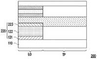
图1A是依照本发明第一实施例的显示面板的俯视示意图。图1B是沿着图1A剖线AA’的剖面示意图。为求清晰,图1A仅绘示配置于基板110的布局区LO上第一显示电极121与位于第一显示电极121下方的第一主动元件(有源元件)TFT1、第二主动元件TFT2、扫描线SL以及数据线DL,且图1B省略绘示部分膜层或元件。请同时参照图1A以及图1B,本实施例的显示面板100包括基板110、显示元件120、介电层130以及光学共振(optical resonance)结构140。基板110具有布局区LO以及位于布局区LO以外的透光区TP。显示元件120配置于基板110的布局区LO上。介电层130位于基板110上且覆盖显示元件120。光学共振结构140配置于介电层130上且对应于显示元件120分布。1A is a schematic top view of a display panel according to a first embodiment of the present invention. Fig. 1B is a schematic cross-sectional view along line AA' of Fig. 1A. For clarity, FIG. 1A only shows the
在本实施例中,第一主动元件TFT1、第二主动元件TFT2、扫描线SL、数据线DL和/或类似的电子元件可以位于基板110的布局区LO上,且透光区TP的面积可以大于布局区LO的面积,以使显示面板100的透光度提升,但本发明不限于此。In this embodiment, the first active element TFT1, the second active element TFT2, the scan line SL, the data line DL and/or similar electronic elements may be located on the layout area LO of the
基板110可为具有可见光穿透性的硬质基板110或柔性基板110。举例而言,硬质基板110的材料例如是玻璃或其他硬质材料,柔性基板110材料例如是聚乙烯对苯二甲酸酯(polyethylene terephthalate,PET)、聚亚酰胺(polyimide,PI)、、聚碳酸酯(polycarbonate,PC)、聚酰胺(polyamide,PA)、聚萘二甲酸乙二醇酯(polyethylenenaphthalate,PEN)、聚乙烯亚胺(polyethylenimine,PEI)、聚氨酯(polyurethane,PU)、聚二甲基硅氧烷(polydimethylsiloxane,PDMS)、压克力系(acrylic)聚合物例如是聚甲基丙烯酸甲酯(polymethylmethacrylate,PMMA)等、醚系(ether)聚合物例如是聚醚砜(polyethersulfone,PES)或聚醚醚酮(polyetheretherketone,PEEK)、聚烯(polyolefin)、金属箔(metal foil)、薄玻璃或其他柔性材料,但本发明并不限于此。The
在其他实施例中,基板110可以是包括导电线路和/或其他电子元件(如:主动元件、被动元件、感测元件、通信元件、逻辑操作数件或微机电系统)的载板。举例而言,基板110的布局区LO上可以有多个主动元件TFT1、TFT2、多条扫描线SL以及多条数据线DL。扫描线SL以及数据线DL彼此交越,以定义出各子像素(未绘示)的所在区域。并且,所述的子像素以阵列方式排列以形成像素阵列(未绘示)。各个子像素包含对应的显示元件120及主动元件TFT1、TFT2。值得注意的是,在图1A中,仅示例性的绘示出一组主动元件TFT1、TFT2、一条扫描线SL以及一条数据线DL。本领域技术人员应理解,可依实际设计的需求而调整主动元件TFT1、TFT2、扫描线SL和/或数据线DL的数量。In other embodiments, the
第一主动元件TFT1包括第一通道层(未绘示)、第一闸极(gate)G1、第一源极S1以及第一漏极D1。第二主动元件TFT2包括第二通道层(未绘示)、第二闸极G2、第二源极S2以及第二漏极D2。The first active element TFT1 includes a first channel layer (not shown), a first gate (gate) G1, a first source electrode S1 and a first drain electrode D1. The second active element TFT2 includes a second channel layer (not shown), a second gate electrode G2, a second source electrode S2 and a second drain electrode D2.
显示元件120包括第一显示电极121、第二显示电极123以及以及位于第一显示电极121与第二显示电极123之间的显示介质层122。The
第一源极S1与对应的数据线DL电性连接。第一闸极G1与对应的扫描线SL电性连接。也就是说,各子像素的第一主动元件TFT1通过所对应的其中一条扫描线SL以及其中一条数据线DL所传送的电信号驱动。The first source electrode S1 is electrically connected to the corresponding data line DL. The first gate electrode G1 is electrically connected to the corresponding scan line SL. That is to say, the first active element TFT1 of each sub-pixel is driven by an electrical signal transmitted by one of the corresponding scan lines SL and one of the data lines DL.
第一漏极D1与第二闸极G2电性连接。第二源极S2与一电压源(VDD,未绘示)电性连接。第二漏极D2与显示元件120的第一显示电极121电性连接,以与各个子像素的第二显示电极123驱动显示介质层122。在本实施例中,第二显示电极123可以是以全面性地分布于基板110上的共享电极,并且可接地或电性连接至共同电压(common voltage;Vcom),但本发明不限于此。The first drain electrode D1 is electrically connected to the second gate electrode G2. The second source S2 is electrically connected to a voltage source (VDD, not shown). The second drain electrode D2 is electrically connected to the
在本实施例中,第一显示电极121以及第二显示电极123的材质可以是铟锡氧化物(indium tin oxide,ITO)、铟锌氧化物(indium zinc oxide,IZO)、氧化铝锌(Al dopedZnO,AZO)、掺镓氧化锌(Ga doped zinc oxide,GZO)、锌锡氧化物(Zinc-Tin Oxide,ZTO)、氟掺杂氧化锡(fluorine-doped tin oxide,FTO)、氧化铟(In2O3)、氧化锌(ZnO)、二氧化锡(SnO2)、氧化钛(TiO2)、有机导电高分子(如PEDOT:PSS)、纳米碳管(CNTs)、金属(如:纳米银线(Silvernanowire))或其他的透明导电材质,但本发明并不限于此。在其他实施例中,第一显示电极121或第二显示电极123可采用金属或金属氧化物等导电材质。倘若第一显示电极121以及第二显示电极123两者皆采用透明导电材质,那么所形成的显示面板100可以构成双面发光显示装置。倘若第一显示电极121或第二显示电极123其中之一采用透明导电材质,那么所形成的显示面板100可以构成底部发光型或是顶部发光型的显示装置。In this embodiment, the material of the
在本实施例中,介电层130可以是由一无机材料所构成,其包含:氧化硅(SiOx)、氮化硅(SiNx)、氮氧化硅(SiON)、氧化铝(AlOx)、氮氧化铝(AlON)或是其他类似物。于其他实施例中,介电层130可以是由一有机材料所构成,其包含:聚亚酰胺(polyimide,PI)、聚碳酸酯(polycarbonate,PC)、聚酰胺(polyamide,PA)、聚对苯二甲酸乙二酯(polyethyleneterephthalate,PET)、聚萘二甲酸乙二醇酯(polyethylene naphthalate,PEN)、聚乙烯亚胺(polyethylenimine,PEI)、聚氨酯(polyurethane,PU)、聚二甲基硅氧烷(polydimethylsiloxane,PDMS)、压克力系(acrylate)聚合物例如是聚甲基丙烯酸甲酯(polymethylmethacrylate,PMMA)等、醚系(ether)聚合物例如是聚醚砜(polyethersulfone,PES)或聚醚醚酮(polyetheretherketone,PEEK)等、聚烯(polyolefin)、光阻或是其他类似物或其组合。于其他可行的实施例中,有机材料和无机材料可交替堆栈以形成介电层130。介电层130形成于显示元件120以及光学共振结构140之间,介电层130可用以分隔显示元件120以及光学共振结构140。In this embodiment, the
光学共振结构140包括堆栈于显示元件120上且彼此分离的第一半透层(transflective layer)141以及第二半透层143。第一半透层141以及第二半透层143之间具有透光层142,且透光层142的相对两端分别与第一半透层141以及第二半透层143相接触。第一半透层141以及第二半透层143为半穿透半反射(transflective)薄膜。透光层142可以为类似于介电层130的透明绝缘层或类似于第一显示电极121/第二显示电极123的透明导电层,于本发明不限于此。第一半透层141以及第二半透层143通过透光层142而彼此分离且具有一间距,以构成具有光学微共振腔(optical microcavity)性质的光学共振结构140,因此可以提升显示元件120所发出的颜色光的一致性(coherence)。The optical resonance structure 140 includes a
在本实施例中,第一半透层141以及第二半透层143的材料例如是镁银合金,以使第一半透层141以及第二半透层143为具有导电及半穿透半反射性质的半穿透半反射电极,但本发明不限于此。在其他实施例中,第一半透层141以及第二半透层143也可以是由相互堆栈的绝缘薄膜所构成半穿透半反射薄膜。倘若第一半透层141和/或第二半透层143采用导电材质,那么第一半透层141和/或第二半透层143也可以是构成其他电子元件(如:主动元件、被动元件、感测元件、通信元件、逻辑操作数件或微机电系统)的一部分。In this embodiment, the material of the first
一般而言,第一半透层141以及第二半透层143的厚度可以依据其材质调整,以使第一半透层141以及第二半透层143具有较佳的半穿透半反射性质。以具有镁银合金材质的第一半透层141以及第二半透层143为例,在显示元件120所发出的光线为可见光的范围内,第一半透层141以及第二半透层143的厚度分别介于5纳米(nanometer;nm)至10纳米,但本发明不限于此。Generally speaking, the thicknesses of the first
除此之外,显示元件120与光学共振结构140的尺寸(如:长度或宽度)及彼此之间的相对位置需有对应的关系,以使显示元件120所发出的光线可以通过对应的光学共振结构140来提升其色彩饱和度。举例而言,在本实施例中,光学共振结构140具有第一宽度Ws,介电层130具有第一厚度LTFE以及第一折射率nTFE,光射出光学共振结构140后所穿过的出射介质(如:后述的硬涂层170)具有第二折射率nout,且上述的第一宽度Ws、第一厚度LTFE、第一折射率nTFE以及第二折射率nout之间的关系可由方程式(1)来表示:In addition, the dimensions (eg, length or width) and the relative positions of the

透过配置于介电层130上且对应于显示元件120分布的光学共振结构140,本实施例可提升显示面板100的色彩饱和度。Through the optical resonance structures 140 disposed on the
一般而言,显示元件120上可以配置硬涂层170,以避免位于硬涂层170之下的显示元件120、光学共振结构140和/或其他膜层的磨损或受到撞击。硬涂层170可以是由有机(organic)材料和/或无机(inorganic)材料所构成,有机材料的折射率可以例如是介于1.4至1.8之间,无机材料的折射率可以例如是介于1.3至2.2之间,但本发明不限于此。In general, the
图2是依照本发明第二实施例的显示面板的剖面示意图。第二实施例的显示面板200与图1的显示面板100类似,本实施例采用图2针对显示面板200进行描述。值得注意的是,在图2中,相同或相似的标号表示相同或相似的构件,故针对图1中说明过的构件于此不再赘述。2 is a schematic cross-sectional view of a display panel according to a second embodiment of the present invention. The
请参照图2,第二实施例的显示面板200与图1的显示面板100类似,显示元件220的第二显示电极223配置于基板110的布局区LO上。换言之,第二显示电极223远离于基板110的透光区TP配置。Referring to FIG. 2 , the
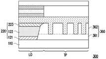
图3是依照本发明第三实施例的显示面板的剖面示意图。第三实施例的显示面板300与图2的显示面板200类似,本实施例采用图3针对显示面板300进行描述。值得注意的是,在图3中,相同或相似的标号表示相同或相似的构件,故针对图2中说明过的构件于此不再赘述。3 is a schematic cross-sectional view of a display panel according to a third embodiment of the present invention. The
请参照图3,第三实施例的显示面板300与图2的显示面板200类似,显示面板300还包括配置于基板110的透光区TP上的导光结构360。导光结构360可以是由光学膜层361以及多个光学微结构362所组成,其中光学膜层361例如是扩散膜。光学微结构362配置于光学膜层361上。在一些实施例中,光学微结构362的密度由邻近显示元件220的一侧往远离显示元件220的一侧逐渐递增。如此一来,可以减少暗区及亮区之间的亮度差异,显示元件220所产生的光线可均匀地被导出,进而提升显示面板300在有效照明区域中的亮度,据以提高正向亮度(luminance)。Referring to FIG. 3 , the
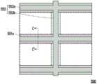
图4A是依照本发明第四实施例的感测显示面板的俯视示意图。图4B是沿着图4A剖线BB’的剖面示意图。为求清晰,图4A省略绘示部分膜层。第四实施例的感测显示面板400与图1的显示面板100类似,本实施例采用图4A与图4B针对感测显示面板400进行描述。值得注意的是,在图4A与图4B中,相同或相似的标号表示相同或相似的构件,故针对图1中说明过的构件于此不再赘述。4A is a schematic top view of a sensing display panel according to a fourth embodiment of the present invention. Fig. 4B is a schematic cross-sectional view along line BB' of Fig. 4A. For clarity, some film layers are omitted in FIG. 4A . The
请同时参照图4A与图4B,第四实施例的感测显示面板400与图1的显示面板100类似,感测显示面板400为包括感测元件450且具有对应于显示元件120分布的光学共振结构140。4A and 4B at the same time, the
感测元件450可用于侦测使用者在触碰感测显示面板400时所产生的信号,此信号类型例如是电容变化、电压变化等。以电容式感测为例,当使用者触碰感测显示面板400时,感测元件450在其被触碰的区域可产生电容的变化,前述的电容变化可被与第一感测线路451和/或第二感测线路452连结的控制器所监测及辨识。以压电式感测为例,当使用者触碰感测显示面板400时,感测元件450在其被触碰的区域可具有对应的形变而产生电压的变化,前述的电压变化可被与第一感测线路451和/或第二感测线路452连结的控制器(未绘示)所监测及辨识。The
在本实施例中,感测元件450包括相互电性绝缘的第一感测线路451以及第二感测线路452,其中第一感测线路451和/或第二感测线路452可为光学共振结构140的第一半透层141与第二半透层143所构成。换言之,第一感测线路451和/或第二感测线路452可以包括堆栈于显示元件120上以形成光学共振结构140的第一感测部分以及第二感测部分,其中第一感测部分即为光学共振结构140的第一半透层141,第二感测部分即为光学共振结构140的第二半透层143,且第一半透层141与第二半透层143皆为半透电极。在一些实施例中,光学共振结构140的透光层142可以为透明导电层,可使由第一半透层141与第二半透层143构成的第一感测线路451和/或第二感测线路452具有较佳的导电性。In this embodiment, the
在本实施例中,第一感测线路451例如是具有多个相同延伸方向的第一感测电极451a以及具有多个相同延伸方向的第二感测电极451b,其中第一感测电极451a的延伸方向可实质上垂直于第二感测电极451b的延伸方向。第二感测线路452例如是具有多个相同延伸方向的第三感测电极452a以及具有多个相同延伸方向的第四感测电极452b,其中第三感测电极452a的延伸方向可实质上垂直于第四感测电极452b的延伸方向。第一感测电极451a的延伸方向可实质上平行于第三感测电极452a的延伸方向,第二感测电极451b的延伸方向可实质上平行于第四感测电极452b的延伸方向。In this embodiment, the
相邻的两个透光区TP之间可以具有多个第一感测电极451a和/或多个第二感测电极451b。第三感测电极452a可以位于相邻的两个第一感测电极451a之间。第四感测电极452b可以位于相邻的两个第二感测电极451b之间,且前述的第二感测电极451b与第四感测电极452b可以对应于同一布局区LO。但本发明对于第一感测线路451和/或第二感测线路452的线路布局(layout)并不加以限制。There may be a plurality of
图5A是依照本发明第五实施例的感测显示面板的俯视示意图。图5B是沿着图5A剖线CC’的剖面示意图。为求清晰,图5A省略绘示部分膜层。第五实施例的感测显示面板500与图1的感测显示面板100类似,本实施例采用图5A与图5B针对感测显示面板500进行描述。值得注意的是,在图5A与图5B中,相同或相似的标号表示相同或相似的构件,故针对图1中说明过的构件于此不再赘述。5A is a schematic top view of a sensing display panel according to a fifth embodiment of the present invention. Fig. 5B is a schematic cross-sectional view taken along line CC' of Fig. 5A. For clarity, some film layers are omitted in FIG. 5A . The
请同时参照图5A与图5B,第四实施例的感测显示面板500与图1的感测显示面板100类似,感测显示面板500为包括感测元件550且具有对应于显示元件120分布的光学共振结构140。Please refer to FIG. 5A and FIG. 5B at the same time, the
在本实施例中,感测元件550包括相互电性绝缘的第一感测线路551以及第二感测线路552,其中第一感测线路551为光学共振结构140的第一半透层141所构成,且第二感测线路552为光学共振结构140的第二半透层143所构成。换言之,感测元件550的第一感测线路551以及第二感测线路552可以堆栈于所述显示元件120上以形成光学共振结构140,且形成光学共振结构140的第一感测线路551以及第二感测线路552包括半透电极。除此之外,在本实施例中,光学共振结构140的透光层142可为透明绝缘层,以使由第一半透层141与第二半透层143分别构成的第一感测线路551与第二感测线路552可彼此电性绝缘。In this embodiment, the
在本实施例中,第一感测线路551例如是具有多个相同延伸方向的第一感测电极551a。第二感测线路552例如是具有多个相同延伸方向的第三感测电极552a以及第四感测电极552b。第三感测电极552a的延伸方向可实质上垂直于第四感测电极552b的延伸方向,第一感测电极551a的延伸方向可实质上平行于第三感测电极552a的延伸方向。In this embodiment, the
在本实施例中,第一感测电极551a的面积可以大于第三感测电极552a的面积,以降低第二显示电极123对于第三感测电极552a之信号干扰,但本发明不限于此。In this embodiment, the area of the
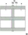
图6是依照本发明第六实施例的感测显示面板的俯视示意图。为求清晰,图6省略绘示部分膜层。第六实施例的感测显示面板600与图5的感测显示面板500类似,本实施例采用图6针对感测显示面板600进行描述。值得注意的是,在图6中,相同或相似的标号表示相同或相似的构件,故针对图5中说明过的构件于此不再赘述。6 is a schematic top view of a sensing display panel according to a sixth embodiment of the present invention. For clarity, some film layers are omitted in FIG. 6 . The
请参照图6,第六实施例的感测显示面板600与图5的感测显示面板500类似,第二感测线路652例如是具有多个相同延伸方向的第三感测电极652a以及具有多个相同延伸方向的第四感测电极652b。相邻的两个透光区TP之间可以具有多个第四感测电极652b,且前述的多个第四感测电极652b可以彼此分离。Referring to FIG. 6 , the
图7是依照本发明第七实施例的感测显示面板的俯视示意图。为求清晰,图7省略绘示部分膜层。第七实施例的感测显示面板700与图6的感测显示面板600类似,本实施例采用图7针对感测显示面板700进行描述。值得注意的是,在图7中,相同或相似的标号表示相同或相似的构件,故针对图6中说明过的构件于此不再赘述。7 is a schematic top view of a sensing display panel according to a seventh embodiment of the present invention. For clarity, some film layers are omitted in FIG. 7 . The
请参照图7,第七实施例的感测显示面板700与图6的感测显示面板600类似,第一感测线路751例如是具有多个相同延伸方向的第一感测电极751a以及具有多个相同延伸方向的第二感测电极751b,其中第一感测电极751a的延伸方向可实质上垂直于第二感测电极751b的延伸方向。第一感测电极751a的延伸方向可实质上平行于第三感测电极652a的延伸方向,第二感测电极751b的延伸方向可实质上平行于第四感测电极652b的延伸方向。多个彼此分离的第二感测电极751b可以与多个彼此分离的第四感测电极652b对应于同一布局区LO,且前述的第二感测电极751b与第四感测电极652b可以彼此重叠。Referring to FIG. 7 , the
图8是依照本发明第八实施例的感测显示面板的俯视示意图。为求清晰,图8省略绘示部分膜层。第八实施例的感测显示面板800与图6的感测显示面板600类似,本实施例采用图8针对感测显示面板800进行描述。值得注意的是,在图8中,相同或相似的标号表示相同或相似的构件,故针对图6中说明过的构件于此不再赘述。8 is a schematic top view of a sensing display panel according to an eighth embodiment of the present invention. For clarity, some film layers are omitted in FIG. 8 . The
请参照图8,第八实施例的感测显示面板800与图6的感测显示面板600类似,于第一感测线路851中,部分相邻的两个第一感测电极851a之间可以具有第二感测电极851b而彼此连接。Referring to FIG. 8 , the
图9是依照本发明第九实施例的感测显示面板的俯视示意图。为求清晰,图9省略绘示部分膜层。第九实施例的感测显示面板900与图7的感测显示面板700类似,本实施例采用图9针对感测显示面板900进行描述。值得注意的是,在图9中,相同或相似的标号表示相同或相似的构件,故针对图7中说明过的构件于此不再赘述。9 is a schematic top view of a sensing display panel according to a ninth embodiment of the present invention. For clarity, some film layers are omitted in FIG. 9 . The
请参照图9,第九实施例的感测显示面板900与图7的感测显示面板700类似,多个彼此分离的第二感测电极951b可以与多个彼此分离的第四感测电极652b对应于同一布局区LO,且前述的第二感测电极951b与第四感测电极652b可以彼此不重叠。Referring to FIG. 9 , the
图10是依照本发明第十实施例的感测显示面板的俯视示意图。为求清晰,图10省略绘示部分膜层。第十实施例的感测显示面板1000与图5A或图5B的感测显示面板500类似,本实施例采用图10针对感测显示面板1000进行描述。值得注意的是,在图10中,相同或相似的标号表示相同或相似的构件,故针对图5A或图5B中说明过的构件于此不再赘述。FIG. 10 is a schematic top view of a sensing display panel according to a tenth embodiment of the present invention. For clarity, some film layers are omitted in FIG. 10 . The
请参照图10,第十实施例的感测显示面板1000与图5A或图5B的感测显示面板500类似,感测显示面板1000具有第一感测区TR1以及第二感测区TR2。位于第一感测区TR1的第二感测线路1052与位于第二感测区TR2的第二感测线路1052'彼此分离。Referring to FIG. 10 , the
图11是依照本发明第十一实施例的感测显示面板的俯视示意图。为求清晰,图11省略绘示部分膜层。第十一实施例的感测显示面板1100与图5A或图5B的感测显示面板500类似,本实施例采用图11针对感测显示面板1100进行描述。值得注意的是,在图11中,相同或相似的标号表示相同或相似的构件,故针对图5A或图5B中说明过的构件于此不再赘述。11 is a schematic top view of a sensing display panel according to an eleventh embodiment of the present invention. For clarity, some film layers are omitted in FIG. 11 . The sensing display panel 1100 of the eleventh embodiment is similar to the
请参照图11,第十一实施例的感测显示面板1100与图5A或图5B的感测显示面板500类似,感测显示面板1100具有第一感测区TR1以及第二感测区TR2。位于第一感测区TR1的第一感测线路1151与位于第二感测区TR2的第一感测线路1151'彼此分离。Referring to FIG. 11 , the sensing display panel 1100 of the eleventh embodiment is similar to the
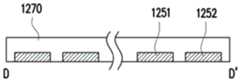
图12A是依照本发明第十二实施例的感测显示面板的俯视示意图。图12B是沿着图12A剖线DD’的剖面示意图。为求清晰,图12A省略绘示部分膜层。第十二实施例的感测显示面板1200与图4A或图4B的感测显示面板400类似,本实施例采用图12A与图12B针对感测显示面板1200进行描述。值得注意的是,在图12A与图12B中,相同或相似的标号表示相同或相似的构件,故针对图4A或图4B中说明过的构件于此不再赘述。12A is a schematic top view of a sensing display panel according to a twelfth embodiment of the present invention. Fig. 12B is a schematic cross-sectional view along line DD' of Fig. 12A. For clarity, some film layers are omitted in FIG. 12A . The
请同时参照图12A与图12B,第十二实施例的感测显示面板1200与图4A或图4B的感测显示面板400类似,第一感测线路1251以及第二感测线路1252为单层的图案化导电层。12A and 12B at the same time, the
第一感测线路1251和/或第二感测线路1252可以与其他的半透层(未绘示)堆栈以构成光学共振结构140。在本实施例中,第一感测线路1251以及第二感测线路1252可以为同一图案化导电层,但本发明不限于此。The
在本实施例中,感测显示面板1200还包括覆盖于第一感测线路1251和/或第二感测线路1252上的绝缘层1270,且绝缘层更可位于第一感测线路1251与第二感测线路1252之间。In this embodiment, the
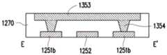
图13A是依照本发明第十三实施例的感测显示面板的俯视示意图。图13B是沿着图13A剖线EE’的剖面示意图。为求清晰,图13A省略绘示部分膜层。第十三实施例的感测显示面板1300与图12A或图12B的感测显示面板1200类似,本实施例采用图13A与图13B针对感测显示面板1300进行描述。值得注意的是,在图13A与图13B中,相同或相似的标号表示相同或相似的构件,故针对图12A或图12B中说明过的构件于此不再赘述。13A is a schematic top view of a sensing display panel according to a thirteenth embodiment of the present invention. Fig. 13B is a schematic cross-sectional view along line EE' of Fig. 13A. For clarity, some film layers are omitted in FIG. 13A . The
请同时参照图13A与图13B,第十三实施例的感测显示面板1300与图12A或图12B的感测显示面板1200类似,感测显示面板1300还包括位于布局区LO的桥接电极1353。13A and 13B at the same time, the
绝缘层1270位于桥接电极1353与第一感测线路1251之间以及桥接电极1353与第二感测线路1252之间。多个导电通孔1354贯穿绝缘层1270,位于第二感测线路1252相对两侧的第一感测线路1251可以通过多个导电通孔1354以与对应的桥接电极1353电性连接。The insulating
在本实施例中,第一感测线路1251以及第二感测线路1252位于桥接电极1353与基板110(绘示于图1B、2或3等类似实施例图示)之间,但本发明不限于此。在其他实施例中,桥接电极1353也可以位于第一感测线路1251和/或第二感测线路1252与基板110之间。In this embodiment, the
在本实施例中,桥接电极1353的延伸方向实质上平行于第一感测电极1251a的延伸方向(延伸方向类似于前述第一感测电极451a),但本发明不限于此。在其他实施例中,桥接电极1353的延伸方向实质上平行于第二感测电极1251b的延伸方向(延伸方向类似于前述第二感测电极451b)。In this embodiment, the extending direction of the
图14是依照本发明第十四实施例的感测显示面板的俯视示意图。为求清晰,图14省略绘示部分膜层。第十四实施例的感测显示面板1400与图13A或图13B的感测显示面板1300类似,本实施例采用图14针对感测显示面板1400进行描述。值得注意的是,在图14中,相同或相似的标号表示相同或相似的构件,故针对图13A或图13B中说明过的构件于此不再赘述。14 is a schematic top view of a sensing display panel according to a fourteenth embodiment of the present invention. For clarity, some film layers are omitted in FIG. 14 . The
请参照图14,第十四实施例的感测显示面板1400与图13A或图13B的感测显示面板1300类似,桥接电极1453的延伸方向实质上平行于第二感测电极1251b的延伸方向。Referring to FIG. 14 , the
图15是依照本发明第十五实施例的感测显示面板的俯视示意图。为求清晰,图15省略绘示部分膜层。第十五实施例的感测显示面板1500与图12A或图12B的感测显示面板1200类似,本实施例采用图15针对感测显示面板1500进行描述。值得注意的是,在图15中,相同或相似的标号表示相同或相似的构件,故针对图12A或图12B中说明过的构件于此不再赘述。15 is a schematic top view of a sensing display panel according to a fifteenth embodiment of the present invention. For clarity, some film layers are omitted in FIG. 15 . The
请参照图15,第十五实施例的感测显示面板1500与图12A或图12B的感测显示面板1200类似,相邻的两个第一感测电极1551a通过对应的第二感测电极1551b而彼此连接,位于布局区LO的第一感测线路1551呈现蜿蜒状分布。Referring to FIG. 15 , the
图16是依照本发明第十六实施例的感测显示面板的俯视示意图。为求清晰,图16省略绘示部分膜层。第十六实施例的感测显示面板1600与图13A或图13B的感测显示面板1300类似,本实施例采用图16针对感测显示面板1600进行描述。值得注意的是,在图16中,相同或相似的标号表示相同或相似的构件,故针对图13A或图13B中说明过的构件于此不再赘述。16 is a schematic top view of a sensing display panel according to a sixteenth embodiment of the present invention. For clarity, some film layers are omitted in FIG. 16 . The
请参照图16,第十六实施例的感测显示面板1600与图13A或图13B的感测显示面板1300类似,位于第二感测电极1251b相对两侧的第三感测电极1252a可以通过桥接电极1653而彼此电性连接。Referring to FIG. 16 , the
图17是依照本发明第十七实施例的感测显示面板的俯视示意图。为求清晰,图17省略绘示部分膜层。第十七实施例的感测显示面板1700与图14的感测显示面板1400类似,本实施例采用图17针对感测显示面板1700进行描述。值得注意的是,在图17中,相同或相似的标号表示相同或相似的构件,故针对图14中说明过的构件于此不再赘述。17 is a schematic top view of a sensing display panel according to a seventeenth embodiment of the present invention. For clarity, some film layers are omitted in FIG. 17 . The
请参照图17,第十七实施例的感测显示面板1700与图14的感测显示面板1400类似,第一感测线路1751和/或第二感测线路1752可以为多个条状电极,且位于第一感测线路1751相对两侧的第二感测线路1752可以通过桥接电极1753而彼此电性连接。Referring to FIG. 17 , the
以下列测试例作为说明本发明实施例的显示面板或感测显示面板可以提升显示面板或感测显示面板的色彩饱和度。然而,这些测试例在任何意义上均不解释为限制本发明之范畴。The following test examples are used to illustrate that the display panel or the sensing display panel according to the embodiment of the present invention can improve the color saturation of the display panel or the sensing display panel. However, these test examples are not to be construed as limiting the scope of the present invention in any sense.
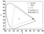
请同时参考图18A至图23B,下列具有光学共振结构的各测试例以及不具有光学共振结构的比较例之间的比较关系,可利用模拟软件估算在上述实施例的显示面板或感测显示面板中,模拟显示元件发出不同具有标准波长的颜色光的状态下,显示面板或感测显示面板的发射光谱比较关系图或色域比较关系图。其中前述的标准波长的颜色光为依据国际照明委员会(International Commission on Illumination;CIE)于公元1931年所制定。而前述的色域比较关系图可以依据国际照明委员会所制定的色度坐标图(CIE 1931colorspace)来表示。Please refer to FIG. 18A to FIG. 23B at the same time, the following comparative relationship between each test example with an optical resonance structure and a comparative example without an optical resonance structure can be estimated by using simulation software in the display panel or sensing display panel of the above embodiment Among them, the comparison diagram of the emission spectrum or the comparison diagram of the color gamut of the display panel or the sensing display panel in the state where the analog display element emits color light with different standard wavelengths. The aforesaid standard wavelength color light was formulated in 1931 AD according to the International Commission on Illumination (CIE). The aforementioned color gamut comparison diagram can be represented according to the chromaticity coordinate diagram (
除此之外,于各测试例中,光学共振结构所具有第一宽度,介电层所具有第一厚度以及第一折射率,以及光射出光学共振结构后所穿过的出射介质(如:硬涂层)具有第二折射率,可符合前述方程式(1)所表示的关系。In addition, in each test example, the optical resonance structure has a first width, the dielectric layer has a first thickness and a first refractive index, and the light exiting the optical resonance structure passes through the output medium (such as: The hard coat layer) has a second refractive index, which can conform to the relationship represented by the aforementioned equation (1).
值得注意的是,以下所表示的数值,可以包括所述数值以及在本领域技术人员可接受的偏差范围内的偏差值。上述偏差值可以是于制造过程或量测过程的一个或多个标准偏差(Standard Deviation),或是于计算或换算过程因采用位数的多寡、四舍五入或经由误差传递(ErrorPropagation)等其他因素所产生的计算误差。It is worth noting that the numerical values expressed below may include the stated numerical values as well as deviations within a range of deviations acceptable to those skilled in the art. The above deviation value can be one or more standard deviations (Standard Deviation) in the manufacturing process or measurement process, or in the calculation or conversion process due to the number of digits used, rounding or other factors such as error propagation (ErrorPropagation) resulting calculation errors.
测试例1:Test case 1:
测试例1与比较例的差别在于测试例1具有光学共振结构,其中构成光学共振结构的第一半透层以及第二半透层其厚度分别为5nm。模拟结果如图18A至图20B以及下列表1所示。The difference between Test Example 1 and Comparative Example is that Test Example 1 has an optical resonance structure, wherein the thicknesses of the first semi-transparent layer and the second semi-transparent layer constituting the optical resonance structure are 5 nm, respectively. The simulation results are shown in FIGS. 18A to 20B and Table 1 below.
图18A、图19A以及图20A分别为测试例1与比较例于显示元件发出红光、绿色、蓝色的状态下,显示面板或感测显示面板的发射光谱比较关系图。其中在上述发射光谱比较关系图中,横轴为发射光波长(单位:nm),纵轴为各波长的发射光的强度(Intensity)对应于具有最大强度的发射光的强度之间的相对强度比值,即各波长的发射光间的相对强度。18A , 19A and 20A are graphs comparing the emission spectra of the display panel or the sensing display panel in Test Example 1 and Comparative Example when the display element emits red light, green light, and blue light, respectively. In the above emission spectrum comparison diagram, the horizontal axis is the wavelength of the emitted light (unit: nm), and the vertical axis is the relative intensity between the intensity of the emitted light of each wavelength (Intensity) corresponding to the intensity of the emitted light with the maximum intensity The ratio, that is, the relative intensities of the emitted light of each wavelength.
图18B、图19B以及图20B分别为测试例1与比较例于显示元件发出红光、绿色、蓝色的状态下,显示面板或感测显示面板的色域比较关系图。其中图18B、图19B以及图20B的色域比较关系图分别对应于图18A、图19A以及图20A的发射光谱比较关系图。在上述色域比较关系图中,马蹄状的实线所围绕(标示为:CIE1931)的区域为一般人类视觉色域的光谱轨迹(spectral locus);虚线所围绕的三角形区域(标示为:NTSC)为美国国家电视系统委员会于公元1953年根据当时的映像管的荧光粉技术定义了红绿蓝三原色色度值,其色度坐标分别为红色(0.67,0.33)、绿色(0.21,0.71)以及蓝色(0.14,0.08);实心点与空心点分别为对应于测试例1与比较例的发射光谱于色度坐标图上的位置;星号为国际照明委员会所定,于色度坐标图中的色度(chromaticity)为白色的标准C光源。18B , FIG. 19B and FIG. 20B are respectively the color gamut comparison diagrams of the display panel or the sensing display panel in the test example 1 and the comparative example when the display element emits red light, green light, and blue light. The color gamut comparison diagrams in FIGS. 18B , 19B and 20B respectively correspond to the emission spectrum comparison diagrams in FIGS. 18A , 19A and 20A . In the above color gamut comparison diagram, the area surrounded by the horseshoe-shaped solid line (marked as: CIE1931) is the spectral locus of the general human visual color gamut; the triangle area surrounded by the dotted line (marked as: NTSC) In 1953, the National Television System Committee of the United States defined the chromaticity values of the three primary colors of red, green and blue according to the phosphor technology of the picture tube at that time. The chromaticity coordinates are red (0.67, 0.33), green (0.21, 0.71) and blue Color (0.14, 0.08); the solid point and the hollow point are the positions on the chromaticity coordinate diagram of the emission spectrum corresponding to Test Example 1 and Comparative Example respectively; the asterisk is determined by the International Commission on Illumination, the color in the chromaticity coordinate diagram A standard C light source whose chromaticity is white.
在下列表1中,红光色度坐标、绿光色度坐标以及蓝光色度坐标的值分别为图18B、图19B以及图20B中,各实心点(测试例1)与空心点(比较例)的色度坐标。色域面积为红光色度坐标、绿光色度坐标以及蓝光色度坐标所围成的三角形面积。NTSC百分比为前述色域面积与虚线所围绕的三角形区域的比值关系。也就是说,若NTSC百分比越接近1,则代表显示面板或感测显示面板的色彩饱和度越接近美国国家电视系统委员会所定义的红绿蓝三原色所呈现的色彩饱和度。In Table 1 below, the values of the red light chromaticity coordinates, the green light chromaticity coordinates, and the blue light chromaticity coordinates are the solid points (Test Example 1) and the hollow points (Comparative Example) in FIGS. 18B , 19B and 20B, respectively. chromaticity coordinates. The color gamut area is the area of the triangle enclosed by the chromaticity coordinates of red light, the chromaticity coordinates of green light, and the chromaticity coordinates of blue light. The NTSC percentage is the ratio of the aforementioned color gamut area to the triangular area surrounded by the dotted line. That is, if the NTSC percentage is closer to 1, it means that the color saturation of the display panel or the sensing display panel is closer to the color saturation presented by the three primary colors of red, green and blue as defined by the National Television System Committee of the United States.
请同时参照图18A至图20B以及下列表1,相较于比较例,测试例1所发光频谱半高宽(Full Width at HalfMaximum;FWHM)较窄。也就是说,经由共振腔结构所产生的法布立-培若效应(Fabry-perot effect)会强化特定波长的出光,以提升显示面板或感测显示面板的色彩饱和度。Please refer to FIGS. 18A to 20B and the following Table 1 at the same time. Compared with the comparative example, the emission spectrum of Test Example 1 has a narrower full width at HalfMaximum (FWHM). That is to say, the Fabry-perot effect generated by the resonant cavity structure can enhance the light output of a specific wavelength, so as to improve the color saturation of the display panel or the sensing display panel.
表1:Table 1:

测试例2:Test case 2:
于测试例2中,构成光学共振结构的第一半透层以及第二半透层其厚度分别为10nm。模拟结果如图21A至图23B以及下列表2所示。In Test Example 2, the thicknesses of the first semi-transparent layer and the second semi-transparent layer constituting the optical resonance structure are respectively 10 nm. The simulation results are shown in FIGS. 21A to 23B and Table 2 below.
图21A至图23B的表示方式分别类似于图18A至图20B,表1的表示方式类似于表2,故于此不加以赘述。The representations of FIGS. 21A to 23B are respectively similar to those of FIGS. 18A to 20B , and the representations of Table 1 are similar to those of Table 2, so they will not be repeated here.
请同时参照图21A至图23B以及下列表2,相较于比较例,测试例2所发光频谱半高宽较窄。也就是说,经由共振腔结构所产生的共振腔效应会强化特定波长的出光,以提升显示面板或感测显示面板的色彩饱和度。Please refer to FIGS. 21A to 23B and the following Table 2 at the same time. Compared with the comparative example, the emission spectrum of Test Example 2 has a narrower half-height width at half maximum. That is to say, the resonant cavity effect generated by the resonant cavity structure can enhance the light output of a specific wavelength, so as to improve the color saturation of the display panel or the sensing display panel.
表2:Table 2:

本发明一实施例的显示面板或感测显示面板可具有光学共振结构,而提升显示面板或感测显示面板的色彩饱和度。除此之外,于本发明一实施例的显示面板或感测显示面板中,电子元件可以位于基板的布局区上,提升显示面板或感测显示面板的开口率或透光率。The display panel or the sensing display panel of an embodiment of the present invention may have an optical resonance structure, so as to improve the color saturation of the display panel or the sensing display panel. In addition, in the display panel or the sensing display panel according to an embodiment of the present invention, the electronic components may be located on the layout area of the substrate to improve the aperture ratio or light transmittance of the display panel or the sensing display panel.
虽然本发明以上述实施例公开,但具体实施例仅用以解释本发明,并不用于限定本发明,任何本技术领域技术人员,在不脱离本发明的构思和范围内,可作一些的变更和完善,故本发明的权利保护范围以权利要求书及其均等范围为准。Although the present invention is disclosed by the above-mentioned embodiments, the specific embodiments are only used to explain the present invention, not to limit the present invention. Any person skilled in the art can make some changes without departing from the spirit and scope of the present invention. Therefore, the scope of the right protection of the present invention is subject to the claims and their equivalents.
Claims (19)
Translated fromChineseApplications Claiming Priority (4)
| Application Number | Priority Date | Filing Date | Title |
|---|---|---|---|
| US201662427820P | 2016-11-30 | 2016-11-30 | |
| US62/427820 | 2016-11-30 | ||
| TW106126809ATWI649598B (en) | 2016-11-30 | 2017-08-09 | Display panel and sensing display panel |
| TW106126809 | 2017-08-09 |
Publications (2)
| Publication Number | Publication Date |
|---|---|
| CN108122487A CN108122487A (en) | 2018-06-05 |
| CN108122487Btrue CN108122487B (en) | 2020-07-17 |
Family
ID=62190800
Family Applications (1)
| Application Number | Title | Priority Date | Filing Date |
|---|---|---|---|
| CN201710929100.6AActiveCN108122487B (en) | 2016-11-30 | 2017-10-09 | Display panel and sensing display panel |
Country Status (2)
| Country | Link |
|---|---|
| US (1) | US10670940B2 (en) |
| CN (1) | CN108122487B (en) |
Families Citing this family (2)
| Publication number | Priority date | Publication date | Assignee | Title |
|---|---|---|---|---|
| CN110930883B (en)* | 2019-12-12 | 2021-09-10 | 昆山国显光电有限公司 | Display panel and display device |
| CN113589972B (en)* | 2021-08-19 | 2023-06-23 | 业成科技(成都)有限公司 | Light-emitting diode screen display structure and light-emitting diode display unit group |
Citations (4)
| Publication number | Priority date | Publication date | Assignee | Title |
|---|---|---|---|---|
| CN1690797A (en)* | 2004-04-29 | 2005-11-02 | 鸿扬光电股份有限公司 | High Brightness Flat Panel Display |
| JP2007232882A (en)* | 2006-02-28 | 2007-09-13 | Casio Comput Co Ltd | Display device and electronic device |
| CN104750285A (en)* | 2013-12-27 | 2015-07-01 | 昆山工研院新型平板显示技术中心有限公司 | Touch display device and preparation method thereof |
| CN106094315A (en)* | 2015-04-30 | 2016-11-09 | 乐金显示有限公司 | There is the display device of PDLC |
Family Cites Families (27)
| Publication number | Priority date | Publication date | Assignee | Title |
|---|---|---|---|---|
| JP4252297B2 (en) | 2002-12-12 | 2009-04-08 | 株式会社日立製作所 | LIGHT EMITTING ELEMENT AND DISPLAY DEVICE USING THE LIGHT EMITTING ELEMENT |
| KR100496286B1 (en) | 2003-04-12 | 2005-06-17 | 삼성에스디아이 주식회사 | Organic electro luminescence display and method for manufacturing the same |
| US20070201234A1 (en) | 2003-07-21 | 2007-08-30 | Clemens Ottermann | Luminous element |
| US20050243023A1 (en) | 2004-04-06 | 2005-11-03 | Damoder Reddy | Color filter integrated with sensor array for flat panel display |
| JP4419691B2 (en)* | 2004-06-02 | 2010-02-24 | セイコーエプソン株式会社 | Organic EL devices, electronic devices |
| KR100704258B1 (en)* | 2004-06-02 | 2007-04-06 | 세이코 엡슨 가부시키가이샤 | Organic EL Devices and Electronic Devices |
| US7572655B2 (en) | 2005-03-23 | 2009-08-11 | E. I. Du Pont De Nemours And Company | Electronic devices having a layer overlying an edge of a different layer and a process for forming the same |
| TWI256745B (en) | 2005-08-31 | 2006-06-11 | Univ Nat Chunghsing | Light-emitting diode with reflection mirror face and manufacturing method thereof |
| TWI317086B (en) | 2006-04-14 | 2009-11-11 | Ritdisplay Corp | Top-emitting organic led display having transparent touch panel |
| KR20110037337A (en) | 2009-10-06 | 2011-04-13 | 엘지디스플레이 주식회사 | Organic light emitting display device and manufacturing method thereof |
| GB2474298A (en) | 2009-10-12 | 2011-04-13 | Iti Scotland Ltd | Light Guide Device |
| US8436833B2 (en) | 2009-11-25 | 2013-05-07 | Corning Incorporated | Methods and apparatus for sensing touch events on a display |
| US9075172B2 (en) | 2010-09-20 | 2015-07-07 | Luxingtek, Ltd. | Light converting optical structure and lighting device utilizing the same |
| US20130093697A1 (en) | 2011-10-18 | 2013-04-18 | Wei-Hao Sun | Touch panel display and assembly process thereof |
| CN104770063A (en) | 2012-10-11 | 2015-07-08 | 松下知识产权经营株式会社 | Organic electroluminescent element and lighting device |
| US9133389B2 (en) | 2012-10-31 | 2015-09-15 | Empire Technology Development Llc | Light guide structure and illuminating device |
| KR101453880B1 (en) | 2012-11-29 | 2014-10-22 | 삼성디스플레이 주식회사 | Organic light emitting display apparatus and the method for manufacturing the same |
| US9240162B2 (en) | 2012-12-31 | 2016-01-19 | Lg Display Co., Ltd. | Transparent display apparatus and method for controlling the same |
| CN104090411B (en)* | 2014-06-19 | 2017-02-15 | 京东方科技集团股份有限公司 | Liquid crystal display panel |
| CN105319641A (en) | 2014-07-31 | 2016-02-10 | 三星Sdi株式会社 | Light guide plate, method for fabricating same, backlight unit, and liquid crystal display |
| JP2016038581A (en)* | 2014-08-08 | 2016-03-22 | 株式会社半導体エネルギー研究所 | Display panel, display device, and method of driving display device |
| TWM500997U (en) | 2014-12-15 | 2015-05-11 | Turnray Energy Tech Ltd | LED flip-chip packaging structure |
| TWI578068B (en) | 2015-01-05 | 2017-04-11 | 穎台科技股份有限公司 | Direct back-lit light guide structure, light guide plate and back-light module |
| US10425464B2 (en) | 2015-01-08 | 2019-09-24 | Instart Logic, Inc. | Adaptive learning periods in HTML streaming |
| CN106033765B (en) | 2015-03-17 | 2019-06-11 | 上海和辉光电有限公司 | Organic Light Emitting Diode touch-control display panel |
| JPWO2016162778A1 (en) | 2015-04-09 | 2018-02-01 | 株式会社半導体エネルギー研究所 | Display device and electronic device |
| TWM508682U (en) | 2015-05-22 | 2015-09-11 | Dayi Optical Technologies Ltd | Light guide bar |
- 2017
- 2017-10-09CNCN201710929100.6Apatent/CN108122487B/enactiveActive
- 2017-10-30USUS15/796,867patent/US10670940B2/enactiveActive
Patent Citations (4)
| Publication number | Priority date | Publication date | Assignee | Title |
|---|---|---|---|---|
| CN1690797A (en)* | 2004-04-29 | 2005-11-02 | 鸿扬光电股份有限公司 | High Brightness Flat Panel Display |
| JP2007232882A (en)* | 2006-02-28 | 2007-09-13 | Casio Comput Co Ltd | Display device and electronic device |
| CN104750285A (en)* | 2013-12-27 | 2015-07-01 | 昆山工研院新型平板显示技术中心有限公司 | Touch display device and preparation method thereof |
| CN106094315A (en)* | 2015-04-30 | 2016-11-09 | 乐金显示有限公司 | There is the display device of PDLC |
Also Published As
| Publication number | Publication date |
|---|---|
| CN108122487A (en) | 2018-06-05 |
| US10670940B2 (en) | 2020-06-02 |
| US20180149944A1 (en) | 2018-05-31 |
Similar Documents
| Publication | Publication Date | Title |
|---|---|---|
| US11430858B2 (en) | Display panel having power bus line with reduced voltage drop | |
| US11093059B2 (en) | Display device | |
| TWI851055B (en) | Light-emitting device and electronic device | |
| US10949047B2 (en) | Display devices | |
| CN111446272A (en) | display device | |
| TW201631566A (en) | Image processing device, display system, and electronic device | |
| KR20150031096A (en) | Display device and method of fabricating the same | |
| US11616215B2 (en) | Display apparatus | |
| US20200161576A1 (en) | Display device | |
| TWI631699B (en) | Illuminating device | |
| CN104731423A (en) | Element substrate | |
| KR20160086487A (en) | Flexible touch panel and flexible display device | |
| CN115942836A (en) | Display module and electronic device comprising same | |
| CN108122487B (en) | Display panel and sensing display panel | |
| CN109994523A (en) | luminous display panel | |
| KR102716143B1 (en) | Display device | |
| TWI827665B (en) | Display devices | |
| TWI649598B (en) | Display panel and sensing display panel | |
| CN110998428B (en) | Shape-dependent convex protrusions in TIR-based image displays | |
| CN219288075U (en) | display screen | |
| US10243028B2 (en) | Organic electroluminescent element and lighting device with buffer layer | |
| KR102344330B1 (en) | Display device | |
| US20240142669A1 (en) | Electronic device | |
| US20240215415A1 (en) | Display device | |
| KR20240144541A (en) | Electronic device and display panel |
Legal Events
| Date | Code | Title | Description |
|---|---|---|---|
| PB01 | Publication | ||
| PB01 | Publication | ||
| SE01 | Entry into force of request for substantive examination | ||
| SE01 | Entry into force of request for substantive examination | ||
| GR01 | Patent grant | ||
| GR01 | Patent grant |