CN108073831B - Method for detecting working state of safety chip and detection circuit - Google Patents
Method for detecting working state of safety chip and detection circuitDownload PDFInfo
- Publication number
- CN108073831B CN108073831BCN201611021892.9ACN201611021892ACN108073831BCN 108073831 BCN108073831 BCN 108073831BCN 201611021892 ACN201611021892 ACN 201611021892ACN 108073831 BCN108073831 BCN 108073831B
- Authority
- CN
- China
- Prior art keywords
- signal
- unit
- circuit
- detection circuit
- security chip
- Prior art date
- Legal status (The legal status is an assumption and is not a legal conclusion. Google has not performed a legal analysis and makes no representation as to the accuracy of the status listed.)
- Active
Links
Images


Classifications
- G—PHYSICS
- G06—COMPUTING OR CALCULATING; COUNTING
- G06F—ELECTRIC DIGITAL DATA PROCESSING
- G06F21/00—Security arrangements for protecting computers, components thereof, programs or data against unauthorised activity
- G06F21/50—Monitoring users, programs or devices to maintain the integrity of platforms, e.g. of processors, firmware or operating systems
- G06F21/57—Certifying or maintaining trusted computer platforms, e.g. secure boots or power-downs, version controls, system software checks, secure updates or assessing vulnerabilities
- G—PHYSICS
- G06—COMPUTING OR CALCULATING; COUNTING
- G06F—ELECTRIC DIGITAL DATA PROCESSING
- G06F21/00—Security arrangements for protecting computers, components thereof, programs or data against unauthorised activity
- G06F21/70—Protecting specific internal or peripheral components, in which the protection of a component leads to protection of the entire computer
- G06F21/71—Protecting specific internal or peripheral components, in which the protection of a component leads to protection of the entire computer to assure secure computing or processing of information
- G06F21/72—Protecting specific internal or peripheral components, in which the protection of a component leads to protection of the entire computer to assure secure computing or processing of information in cryptographic circuits
- G—PHYSICS
- G06—COMPUTING OR CALCULATING; COUNTING
- G06F—ELECTRIC DIGITAL DATA PROCESSING
- G06F21/00—Security arrangements for protecting computers, components thereof, programs or data against unauthorised activity
- G06F21/70—Protecting specific internal or peripheral components, in which the protection of a component leads to protection of the entire computer
- G06F21/71—Protecting specific internal or peripheral components, in which the protection of a component leads to protection of the entire computer to assure secure computing or processing of information
- G06F21/75—Protecting specific internal or peripheral components, in which the protection of a component leads to protection of the entire computer to assure secure computing or processing of information by inhibiting the analysis of circuitry or operation
- G—PHYSICS
- G06—COMPUTING OR CALCULATING; COUNTING
- G06F—ELECTRIC DIGITAL DATA PROCESSING
- G06F1/00—Details not covered by groups G06F3/00 - G06F13/00 and G06F21/00
- G06F1/04—Generating or distributing clock signals or signals derived directly therefrom
- G06F1/06—Clock generators producing several clock signals
- G—PHYSICS
- G06—COMPUTING OR CALCULATING; COUNTING
- G06F—ELECTRIC DIGITAL DATA PROCESSING
- G06F11/00—Error detection; Error correction; Monitoring
- G06F11/30—Monitoring
- G06F11/3003—Monitoring arrangements specially adapted to the computing system or computing system component being monitored
- G06F11/3024—Monitoring arrangements specially adapted to the computing system or computing system component being monitored where the computing system component is a central processing unit [CPU]
- G—PHYSICS
- G06—COMPUTING OR CALCULATING; COUNTING
- G06F—ELECTRIC DIGITAL DATA PROCESSING
- G06F11/00—Error detection; Error correction; Monitoring
- G06F11/30—Monitoring
- G06F11/3058—Monitoring arrangements for monitoring environmental properties or parameters of the computing system or of the computing system component, e.g. monitoring of power, currents, temperature, humidity, position, vibrations
- G—PHYSICS
- G06—COMPUTING OR CALCULATING; COUNTING
- G06F—ELECTRIC DIGITAL DATA PROCESSING
- G06F11/00—Error detection; Error correction; Monitoring
- G06F11/30—Monitoring
- G06F11/34—Recording or statistical evaluation of computer activity, e.g. of down time, of input/output operation ; Recording or statistical evaluation of user activity, e.g. usability assessment
- G06F11/3466—Performance evaluation by tracing or monitoring
- G06F11/348—Circuit details, i.e. tracer hardware
- G—PHYSICS
- G06—COMPUTING OR CALCULATING; COUNTING
- G06F—ELECTRIC DIGITAL DATA PROCESSING
- G06F11/00—Error detection; Error correction; Monitoring
- G06F11/30—Monitoring
- G06F11/34—Recording or statistical evaluation of computer activity, e.g. of down time, of input/output operation ; Recording or statistical evaluation of user activity, e.g. usability assessment
- G06F11/3466—Performance evaluation by tracing or monitoring
- G06F11/3495—Performance evaluation by tracing or monitoring for systems
- G—PHYSICS
- G06—COMPUTING OR CALCULATING; COUNTING
- G06F—ELECTRIC DIGITAL DATA PROCESSING
- G06F2221/00—Indexing scheme relating to security arrangements for protecting computers, components thereof, programs or data against unauthorised activity
- G06F2221/03—Indexing scheme relating to G06F21/50, monitoring users, programs or devices to maintain the integrity of platforms
- G06F2221/034—Test or assess a computer or a system
Landscapes
- Engineering & Computer Science (AREA)
- Theoretical Computer Science (AREA)
- Physics & Mathematics (AREA)
- General Engineering & Computer Science (AREA)
- Computer Hardware Design (AREA)
- General Physics & Mathematics (AREA)
- Software Systems (AREA)
- Computer Security & Cryptography (AREA)
- Mathematical Physics (AREA)
- Quality & Reliability (AREA)
- Computing Systems (AREA)
- Semiconductor Integrated Circuits (AREA)
- Electronic Switches (AREA)
Abstract
Translated fromChinese
Description
Translated fromChinese技术领域technical field
本发明实施例涉及信息安全技术领域,尤其涉及一种检测安全芯片工作状态的方法、检测电路及安全芯片。Embodiments of the present invention relate to the technical field of information security, and in particular, to a method for detecting a working state of a security chip, a detection circuit and a security chip.
背景技术Background technique
安全芯片是对存储在安全芯片里的数据进行高可靠性的加密处理,使这些数据很难被非法窃取,其工作时所处的工作环境(Operating Condition)(例如,电气环境)需要保证该安全芯片内的电路(例如,CPU电路、加解密电路、随机数生成电路等)正常运转。一旦该安全芯片工作的电气环境的某个参数超过安全芯片内的电路的耐受阈值,则安全芯片内的电路运转可能会发生异常,此种情况下可能会导致安全芯片所存储的数据泄露。The security chip performs high-reliability encryption processing on the data stored in the security chip, making it difficult for these data to be illegally stolen. The circuits in the chip (for example, the CPU circuit, the encryption/decryption circuit, the random number generation circuit, etc.) operate normally. Once a certain parameter of the electrical environment in which the security chip operates exceeds the tolerance threshold of the circuit in the security chip, the circuit in the security chip may operate abnormally, which may lead to leakage of data stored in the security chip.
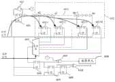
目前,安全芯片内集成了各类传感器(sensor),分别用于监测安全芯片工作时所处的工作环境的各个环境分量(例如,电压、温度、光和时钟信息),然后将各个环境分量通过信号处理模块进行分析,判断该安全芯片所处的工作环境是否合理,若不合理则报警。但是,目前安全芯片内部对上述各个环境分量的监测都是独立进行的,示例性的,如图1所示,例如,使用电压传感器监控电压,使用温度传感器监控温度,使用光传感器监控入射光,使用频率传感器用来监控时钟信息,各个类型的传感器之间相互独立,各类传感器均以模拟电路为主。At present, various types of sensors are integrated in the security chip, which are respectively used to monitor various environmental components (such as voltage, temperature, light and clock information) of the working environment in which the security chip works, and then pass the various environmental components through The signal processing module analyzes and judges whether the working environment in which the security chip is located is reasonable, and if it is unreasonable, an alarm is issued. However, at present, the monitoring of the above-mentioned environmental components in the security chip is carried out independently. For example, as shown in Figure 1, for example, a voltage sensor is used to monitor voltage, a temperature sensor is used to monitor temperature, and a light sensor is used to monitor incident light. The frequency sensor is used to monitor the clock information. Various types of sensors are independent of each other, and all types of sensors are mainly based on analog circuits.
但是,模拟电路的面积一般不能够随工艺演进而明显减小,因此模拟电路的面积越大使得模拟电路更容易在安全芯片版图中被识别出来,存在较高的被攻击风险。However, the area of the analog circuit generally cannot be significantly reduced with the evolution of the process. Therefore, the larger the area of the analog circuit, the easier it is to identify the analog circuit in the security chip layout, and there is a higher risk of being attacked.
发明内容SUMMARY OF THE INVENTION
本发明的实施例提供一种检测安全芯片工作状态的方法及检测电路,用以解决现有技术中模拟电路的面积越大使得模拟电路更容易在安全芯片版图中被识别出来,存在较高的被攻击风险的问题。Embodiments of the present invention provide a method and a detection circuit for detecting the working state of a security chip, so as to solve the problem that the larger the area of the analog circuit in the prior art, the easier the analog circuit is to be identified in the layout of the security chip, and there is a higher the risk of being attacked.
为达到上述目的,本发明的实施例采用如下技术方案:To achieve the above object, the embodiments of the present invention adopt the following technical solutions:
第一方面,本发明实施例提供一种检测安全芯片工作状态的电路,包括:第一寄存单元,与第一寄存单元连接的触发单元和延迟单元,与延迟单元连接的选路单元,与选路单元连接的第二寄存单元,第二寄存单元与触发单元连接;其中,第一寄存单元,用于在时钟信号有效时,根据输入至第一寄存单元的触发信号获取第一信号,以及将第一信号输出至延迟单元和第二逻辑门单元;延迟单元,用于将第一信号延迟不同时间段以产生多个延迟信号,并在时钟信号有效时,根据多个延迟信号生成多个第二信号;选路单元,用于从多个第二信号中选择一个第二信号,并将所选择的第二信号输出至所述第二寄存单元;第二寄存单元,用于在时钟信号有效时,根据接收的第二信号生成第三信号,并将第三信号输出至触发单元;触发单元,用于对第三信号和第一信号进行逻辑运算,获取电平信号,并根据电平信号确定是否输出报警信号。In a first aspect, an embodiment of the present invention provides a circuit for detecting a working state of a security chip, including: a first register unit, a trigger unit and a delay unit connected to the first register unit, a routing unit connected to the delay unit, and a selection unit. The second register unit is connected to the channel unit, and the second register unit is connected to the trigger unit; wherein, the first register unit is used to obtain the first signal according to the trigger signal input to the first register unit when the clock signal is valid, and to The first signal is output to the delay unit and the second logic gate unit; the delay unit is used to delay the first signal by different time periods to generate multiple delay signals, and when the clock signal is valid, generate multiple first signals according to the multiple delay signals. Two signals; a routing unit for selecting a second signal from a plurality of second signals, and outputting the selected second signal to the second register unit; the second register unit for when the clock signal is valid When the second signal is received, the third signal is generated according to the received second signal, and the third signal is output to the trigger unit; the trigger unit is used to perform logical operation on the third signal and the first signal, obtain the level signal, and according to the level signal Determines whether or not to output an alarm signal.
本发明实施例提供一种检测安全芯片工作状态的电路,包括:第一寄存单元,与第一寄存单元连接的触发单元和延迟单元,与延迟单元连接的选路单元,与选路单元连接的第二寄存单元,第二寄存单元与触发单元连接;本发明实施例将第一信号进行延迟以获取多个延迟信号,并根据多个延迟信号生成多个第二信号,通过从多个第二信号中选择一个第二信号,并将所选择的第二信号输出至第二寄存单元获取第三信号,并对所述第三信号和所述第一信号进行逻辑运算,获取电平信号,并根据所述电平信号确定是否输出报警信号,由于本发明实施例中的各个单元均可以通过数字电路来实现,因此可以减小该电路的尺寸,从而使得该电路不易在安全芯片的版图中被识别,提高安全芯片的可靠性,因此可以通过判断第一信号在延迟链路上传输的时延,来确定本发明实施例提供的检测安全芯片工作状态的电路所处的工作状态是否为正常工作条件。An embodiment of the present invention provides a circuit for detecting a working state of a security chip, including: a first register unit, a trigger unit and a delay unit connected to the first register unit, a path selection unit connected to the delay unit, and a circuit selection unit connected to the path selection unit a second register unit, the second register unit is connected to the trigger unit; the embodiment of the present invention delays the first signal to obtain multiple delay signals, and generates multiple second signals according to the multiple delay signals, Selecting a second signal from the signals, and outputting the selected second signal to the second register unit to obtain a third signal, and performing logical operations on the third signal and the first signal to obtain a level signal, and Whether to output an alarm signal is determined according to the level signal. Since each unit in the embodiment of the present invention can be implemented by a digital circuit, the size of the circuit can be reduced, so that the circuit is not easily accessible in the layout of the security chip. identification to improve the reliability of the security chip. Therefore, it can be determined whether the working state of the circuit for detecting the working state of the security chip provided by the embodiment of the present invention is normal operation by judging the time delay of the transmission of the first signal on the delay link. condition.
结合第一方面,在第一方面的第一种可能的实现方式中,选路单元具体用于:接收用于指示从每个第三寄存单元生成的第二信号中选择一个第二信号的选择信号,根据选择信号用于指示从每个第三寄存单元生成的第二信号中选择一个第二信号。该电路的性能边界由第一信号的时延确定,因此,第一信号的延迟不同可以使得该电路具有不同的性能边界,这样可以使得在不同的性能边界时使得处于不同工作状态的检测安全芯片工作状态的电路能够及时检测出该工作状态是否为安全芯片正常的工作状态。With reference to the first aspect, in a first possible implementation manner of the first aspect, the routing unit is specifically configured to: receive a selection for instructing to select one second signal from the second signals generated by each third register unit The signal is used to instruct to select one second signal from the second signals generated by each third register unit according to the selection signal. The performance boundary of the circuit is determined by the delay of the first signal. Therefore, different delays of the first signal can make the circuit have different performance boundaries, which can make the detection security chips in different working states at different performance boundaries. The circuit in the working state can timely detect whether the working state is the normal working state of the security chip.
结合第一方面或第一方面的第一种可能的实现方式,在第一方面的第二种可能的实现方式中,触发单元具体用于:在电平信号为高电平信号时,输出报警信号。In combination with the first aspect or the first possible implementation of the first aspect, in the second possible implementation of the first aspect, the trigger unit is specifically used to: output an alarm when the level signal is a high-level signal Signal.
结合第一方面至第一方面的第二种可能的实现方式中任意一种可能的实现方式,在第一方面的第三种可能的实现方式中,延迟单元包括至少一个第三寄存单元,以及与至少一个第三寄存单元中每个第三寄存单元相连的延迟链路;其中,延迟链路,用于将第一信号延迟不同时间段以产生多个延迟信号,并将多个延迟信号传送至不同的第三寄存单元;每个第三寄存单元,用于接收延迟信号,以及在时钟信号有效时,根据传输至第三寄存单元的延迟信号生成第二信号。With reference to any one possible implementation manner of the first aspect to the second possible implementation manner of the first aspect, in a third possible implementation manner of the first aspect, the delay unit includes at least one third register unit, and a delay link connected to each third register unit in the at least one third register unit; wherein the delay link is used to delay the first signal by different time periods to generate multiple delay signals, and transmit the multiple delay signals to different third register units; each third register unit is used for receiving the delay signal, and when the clock signal is valid, generating the second signal according to the delay signal transmitted to the third register unit.
结合第一方面至第一方面的第三种可能的实现方式中任意一种可能的实现方式,在第一方面的第四种可能的实现方式中,电路还包括反相单元,反相单元的输出端接第一寄存单元的输入端,反相单元的输入端接第一寄存单元的输出端,反相单元用于将第一寄存单元的输出端输出的第一信号进行反相,然后输入至第一寄存单元的输入端。由此保证第一寄存单元的输入端与输出端的信号一致保持相反状态;当时钟信号处于上升沿瞬间时,第一寄存单元将输入端的值搬移到输出端,从而实现输出端信号的一次翻转。With reference to any one possible implementation manner of the first aspect to the third possible implementation manner of the first aspect, in a fourth possible implementation manner of the first aspect, the circuit further includes an inverting unit, and the The output end is connected to the input end of the first register unit, the input end of the inversion unit is connected to the output end of the first register unit, and the inversion unit is used to invert the first signal output by the output end of the first register unit, and then input to the input of the first register unit. Therefore, it is ensured that the input terminal of the first register unit and the signal of the output terminal are in the opposite state; when the clock signal is at the instant of the rising edge, the first register unit moves the value of the input terminal to the output terminal, thereby realizing a flip of the output terminal signal.
结合第一方面至第一方面的第三种可能的实现方式中任意一种可能的实现方式,在第一方面的第四种可能的实现方式中,延迟链路包括多个延迟元件,每个延迟元件用于将输入至该延迟元件的信号延迟预设周期,以使得第一信号经过不同个数的延迟元件后生成不同时间段的延迟信号。With reference to any one possible implementation manner of the first aspect to the third possible implementation manner of the first aspect, in a fourth possible implementation manner of the first aspect, the delay link includes a plurality of delay elements, each of which The delay element is used for delaying the signal input to the delay element by a preset period, so that the first signal generates delay signals of different time periods after passing through different numbers of delay elements.
结合第一方面至第一方面的第四种可能的实现方式中任意一种可能的实现方式,在第一方面的第五种可能的实现方式中,第一寄存单元、第二寄存单元以及第三寄存单元均采用D触发器;选路单元采用MUX复用器。With reference to any one of the possible implementation manners of the first aspect to the fourth possible implementation manner of the first aspect, in the fifth possible implementation manner of the first aspect, the first register unit, the second register unit, and the The three register units all use D flip-flops; the routing unit uses MUX multiplexers.
结合第一方面至第一方面的第五种可能的实现方式中任意一种可能的实现方式,在第一方面的第六种可能的实现方式中,逻辑门单元采用异或门电路。With reference to any possible implementation manner of the first aspect to the fifth possible implementation manner of the first aspect, in the sixth possible implementation manner of the first aspect, the logic gate unit adopts an exclusive OR gate circuit.
结合第一方面至第一方面的第六种可能的实现方式中任意一种可能的实现方式,在第一方面的第七种可能的实现方式中,电路还包括:第四寄存单元、第五寄存单元和第一逻辑门单元;其中,第四寄存单元与第二寄存单元、第五寄存单元以及第一逻辑门单元连接;其中,第四寄存单元用于接收第二寄存单元输出的第三信号,以及在时钟信号有效时生成第四信号,以及将第四信号输出至第五寄存单元以及第一逻辑门单元;第五寄存单元,用于接收第四寄存单元输出的第四信号,以及在时钟信号有效时,根据第四信号生成第五信号,并将第五信号输出至第一逻辑门单元;第一逻辑门单元,用于根据第四信号和第五信号生成触发信号,触发信号用于表明电路内部的元件正常,通过设置第四寄存单元、第五寄存单元和第一逻辑门单元这样可以及时检测电路内部的电路是否处于正常状态,以保种检测安全芯片工作状态的电路正常运行。With reference to any one of the possible implementation manners of the first aspect to the sixth possible implementation manner of the first aspect, in the seventh possible implementation manner of the first aspect, the circuit further includes: a fourth register unit, a fifth possible implementation manner a register unit and a first logic gate unit; wherein the fourth register unit is connected to the second register unit, the fifth register unit and the first logic gate unit; wherein the fourth register unit is used for receiving the third register unit output by the second register unit signal, and generating a fourth signal when the clock signal is valid, and outputting the fourth signal to the fifth register unit and the first logic gate unit; the fifth register unit for receiving the fourth signal output by the fourth register unit, and When the clock signal is valid, a fifth signal is generated according to the fourth signal, and the fifth signal is output to the first logic gate unit; the first logic gate unit is used to generate a trigger signal according to the fourth signal and the fifth signal, and the trigger signal It is used to indicate that the components inside the circuit are normal. By setting the fourth register unit, the fifth register unit and the first logic gate unit, it is possible to detect whether the circuit inside the circuit is in a normal state in time, so as to ensure that the circuit for detecting the working state of the security chip is normal. run.
结合第一方面至第一方面的第七种可能的实现方式中任意一种可能的实现方式,在第一方面的第八种可能的实现方式中,触发单元包括第二逻辑门单元和报警单元,其中,第二逻辑门单元和第一寄存单元相连,报警单元和第二逻辑门单元相连,第二逻辑门单元还与第二寄存单元相连;其中,第二逻辑门单元,用于对第三信号和第一信号进行逻辑运算,获取电平信号,并将电平信号发送至所述报警单元;报警单元,用于根据电平信号确定是否输出报警信号。With reference to any one possible implementation manner of the first aspect to the seventh possible implementation manner of the first aspect, in the eighth possible implementation manner of the first aspect, the trigger unit includes a second logic gate unit and an alarm unit , wherein the second logic gate unit is connected with the first register unit, the alarm unit is connected with the second logic gate unit, and the second logic gate unit is also connected with the second register unit; wherein, the second logic gate unit is used for The three signals and the first signal perform logical operations to obtain a level signal, and send the level signal to the alarm unit; the alarm unit is used for determining whether to output an alarm signal according to the level signal.
第二方面,本发明实施例提供一种检测安全芯片工作状态的方法,应用于检测安全芯片工作状态的电路中,本发明实施例提供的方法包括:在时钟信号有效时,根据输入至检测安全芯片工作状态的电路的触发信号获取第一信号;将第一信号进行延迟,以获取多个延迟信号,其中,多个延迟信号中每个延迟信号的时延均不同;根据多个延迟信号获取多个第二信号;从多个第二信号中选择一个第二信号,在时钟信号有效时,根据所选择的第二信号生成第三信号;在时钟信号有效时,对第一信号和第三信号进行逻辑运算,获取电平信号;根据电平信号确定是否输出报警信号。In a second aspect, an embodiment of the present invention provides a method for detecting the working state of a security chip, which is applied to a circuit for detecting the working state of a security chip. The method provided by the embodiment of the present invention includes: when a clock signal is valid, detecting the security The trigger signal of the circuit in the working state of the chip obtains the first signal; the first signal is delayed to obtain a plurality of delay signals, wherein the delay of each delay signal in the plurality of delay signals is different; and the delay signal is obtained according to the plurality of delay signals a plurality of second signals; one second signal is selected from the plurality of second signals, and when the clock signal is valid, a third signal is generated according to the selected second signal; when the clock signal is valid, the first signal and the third signal are generated according to the selected second signal; Perform logic operation on the signal to obtain the level signal; determine whether to output the alarm signal according to the level signal.
结合第二方面,在第二方面的第一种可能的实现方式中,在从多个第二信号中选择一个第二信号之前,本发明实施例提供的方法还包括:接收用于指示从多个第二信号中选择一个第二信号的选择信号,根据选择信号从多个第二信号中选择一个第二信号。With reference to the second aspect, in a first possible implementation manner of the second aspect, before selecting a second signal from a plurality of second signals, the method provided in this embodiment of the present invention further includes: A selection signal of a second signal is selected from among the second signals, and one second signal is selected from a plurality of second signals according to the selection signal.
结合第二方面或第二方面的第一种可能的实现方式,在第二方面的第二种可能的实现方式中,根据输入至检测安全芯片工作状态的电路的触发信号获取第一信号之后,该方法还包括:将当前时刻输出的第一信号进行反相,以确定下一时刻输入至安全芯片的触发信号。With reference to the second aspect or the first possible implementation manner of the second aspect, in the second possible implementation manner of the second aspect, after obtaining the first signal according to the trigger signal input to the circuit for detecting the working state of the security chip, The method further includes: inverting the first signal output at the current moment to determine the trigger signal input to the security chip at the next moment.
结合第二方面至第二方面的第二种可能的实现方式中任意一种可能的实现方式,在第二方面的第三种可能的实现方式中,根据电平信号确定是否输出报警信号,包括:在电平信号为高电平信号时,则输出报警信号。With reference to any one possible implementation manner of the second aspect to the second possible implementation manner of the second aspect, in a third possible implementation manner of the second aspect, determining whether to output an alarm signal according to the level signal, including : When the level signal is a high level signal, an alarm signal is output.
结合第二方面至第二方面的第三种可能的实现方式中任意一种可能的实现方式,在第二方面的第四种可能的实现方式中,本发明实施例提供的方法还包括:在在时钟信号有效时,根据第三信号生成第五信号;在时钟信号有效时,根据第五信号生成第六信号;根据第五信号和第六信号生成用于表明电路的元件正常的触发信号。With reference to any one possible implementation manner of the second aspect to the third possible implementation manner of the second aspect, in the fourth possible implementation manner of the second aspect, the method provided by the embodiment of the present invention further includes: When the clock signal is valid, a fifth signal is generated according to the third signal; when the clock signal is valid, a sixth signal is generated according to the fifth signal; and a trigger signal indicating that the elements of the circuit are normal is generated according to the fifth signal and the sixth signal.
第三方面,本发明实施例提供一种安全芯片的保护电路,该安全芯片的保护电路应用于安全芯片中,安全芯片包括至少一个检测电路,其中,任意一个检测电路用于检测该检测电路检测范围内的环境状态;检测电路采用如第一方面至第一方面的第七种可能的实现方式中任意一项所描述的检测安全芯片工作状态的电路,并根据环境状态判断是否发出报警信号;检测安全芯片工作状态的电路与安全芯片具有相同的工作条件,工作条件至少包括时钟信号的时钟周期、电源、温度。In a third aspect, an embodiment of the present invention provides a protection circuit for a security chip. The protection circuit for the security chip is applied to the security chip, and the security chip includes at least one detection circuit, wherein any one detection circuit is used to detect the detection circuit detection. The environmental state within the range; the detection circuit adopts the circuit for detecting the working state of the security chip as described in any one of the first aspect to the seventh possible implementation manner of the first aspect, and judges whether to issue an alarm signal according to the environmental state; The circuit for detecting the working state of the security chip has the same working conditions as the security chip, and the working conditions at least include the clock period of the clock signal, the power supply, and the temperature.
本发明实施例一种安全芯片的保护电路,该安全芯片的保护电路应用于安全芯片中,该安全芯片中包括至少一个检测电路,任意一个检测电路用于检测该检测电路检测预设范围内的环境状态,并根据环境状态确定是否发出报警信号,由于该检测电路采用第一方面至第一方面的第七种可能的实现方式中任意一项所描述的检测安全芯片工作状态的电路,该检测安全芯片工作状态的电路能够根据安全芯片所处的工作状态,自动完成实现对安全芯片所处工作状态是都处在安全状态的检测,由于检测安全芯片工作状态的电路内的元器件均采用数字电路,因此,不受老化、工作状态变化的影响;同时,由于检测安全芯片工作状态的电路中采用数字电路可以做的足够小,这样设置在安全芯片内的检测安全芯片工作状态的电路的数量不受安全芯片尺寸所限制,同时在安全芯片内摆放至少一个检测安全芯片工作状态的电路在安全芯片遭到局部工作条件变化时可以及时产生报警,当然,本发明实施例提供的安全芯片在安全芯片所处的整个工作环境发生变化时也可以及时报警。An embodiment of the present invention provides a protection circuit for a security chip. The protection circuit for the security chip is applied to a security chip. The security chip includes at least one detection circuit, and any detection circuit is used to detect the detection circuit within a preset range. environment state, and determine whether to send out an alarm signal according to the environment state. The circuit of the working state of the safety chip can automatically complete the detection of whether the working state of the safety chip is in a safe state according to the working state of the safety chip. Since the components in the circuit for detecting the working state of the safety chip are all digital Therefore, the circuit is not affected by aging and working state changes; at the same time, since the digital circuit used in the circuit for detecting the working state of the security chip can be made small enough, the number of circuits set in the security chip for detecting the working state of the security chip It is not limited by the size of the security chip, and at the same time, at least one circuit for detecting the working state of the security chip is placed in the security chip, and an alarm can be generated in time when the security chip is subjected to changes in local working conditions. When the entire working environment where the security chip is located changes, it can also alarm in time.
结合第三方面,在第三方面的第一种可能的实现方式中,当安全芯片中存在两个或两个以上的检测电路时,该两个或两个以上的检测电路位于不同的位置,通过将检测安全芯片工作状态的电路摆放在安全芯片内的不同位置,由于每个检测安全芯片工作状态的电路均有其所检测的范围,这样当安全芯片的任意一个局部的工作状态发生变化时(例如,安全芯片的某一个局部遭到攻击,使得该局部电压发生变化,但是安全芯片其他位置的电压未发生变化),位于该布局内的安全芯片则可以及时检测到工作状态发生变化,并当该工作状态的变化所引起的电平信号能够触发报警单元时,该报警单元及时发出报警信号。With reference to the third aspect, in a first possible implementation manner of the third aspect, when there are two or more detection circuits in the security chip, the two or more detection circuits are located at different positions, By placing the circuits that detect the working state of the security chip at different positions in the security chip, since each circuit that detects the working state of the security chip has its detection range, when the working state of any part of the security chip changes (for example, a certain part of the security chip is attacked, causing the local voltage to change, but the voltage of other parts of the security chip does not change), the security chip located in the layout can detect the change in the working state in time, And when the level signal caused by the change of the working state can trigger the alarm unit, the alarm unit sends out an alarm signal in time.
第四方面,本发明实施例提供一种安全芯片的检测方法,应用于如本发明实施例第三方面或第三方面的第一种可能的实现方式所描述的安全芯片中,该方法包括:根据输入的选择信号,设定每个检测电路所选择的目标第三寄存单元;该选择信号用于指示选路单元从至少一个第三寄存单元中选择目标第三寄存单元;在安全芯片启动后,若至少一个检测电路中存在任意一个检测电路发出报警信号,则表明安全芯片当前时刻工作在不安全的工作条件下。In a fourth aspect, an embodiment of the present invention provides a method for detecting a security chip, which is applied to the security chip described in the third aspect or the first possible implementation manner of the third aspect of the embodiment of the present invention, and the method includes: According to the input selection signal, the target third register unit selected by each detection circuit is set; the selection signal is used to instruct the routing unit to select the target third register unit from at least one third register unit; after the security chip is activated , if any detection circuit in at least one detection circuit sends an alarm signal, it indicates that the security chip is currently working under unsafe working conditions.
结合第四方面,在第四方面的第一种可能的实现方式中,在至少一个检测电路中存在任意一个检测电路发出报警信号之前,本发明实施例提供的方法还包括:获取至少一个检测电路中每个检测电路当前时刻所处的工作状态;根据每个检测电路当前时刻所处的工作状态与检测电路的性能边界之间的关系,每个检测电路判断是否发出报警信号。With reference to the fourth aspect, in a first possible implementation manner of the fourth aspect, before any one of the detection circuits in the at least one detection circuit sends an alarm signal, the method provided in the embodiment of the present invention further includes: acquiring at least one detection circuit According to the relationship between the working state of each detection circuit at the current moment and the performance boundary of the detection circuit, each detection circuit judges whether to issue an alarm signal.
结合第四方面或第四方面的第一种可能的实现方式中,在第四方面的第二种可能的实现方式中,根据每个检测电路当前时刻所处的工作状态与所述检测电路的性能边界之间的关系,每个检测电路判断是否发出报警信号,包括:当至少一个检测电路中存在第一检测电路当前时刻所处的工作状态位于第一检测电路的性能边界外时,则第一检测电路发出报警信号,第一检测电路为至少一个检测电路中任意一个检测电路。In combination with the fourth aspect or the first possible implementation manner of the fourth aspect, in the second possible implementation manner of the fourth aspect, according to the working state of each detection circuit at the current moment and the detection circuit The relationship between the performance boundaries, each detection circuit determines whether to send an alarm signal, including: when there is at least one detection circuit in which the working state of the first detection circuit at the current moment is outside the performance boundary of the first detection circuit, then the first detection circuit A detection circuit sends out an alarm signal, and the first detection circuit is any one of the at least one detection circuit.
结合第四方面至第四方面的第二种可能的实现方式中任意一种可能的实现方式,在第四方面的第三种可能的实现方式中,根据每个检测电路当前时刻所处的工作状态与所述检测电路的性能边界之间的关系,每个检测电路判断是否发出报警信号,还包括:当至少一个检测电路中存在第一检测电路当前时刻所处的工作状态位于第一检测电路的性能边界内,则第一检测电路不发出报警信号,第一检测电路为至少一个检测电路中任意一个检测电路。With reference to any one possible implementation manner of the fourth aspect to the second possible implementation manner of the fourth aspect, in the third possible implementation manner of the fourth aspect, according to the work of each detection circuit at the current moment The relationship between the state and the performance boundary of the detection circuit, each detection circuit judges whether to send an alarm signal, and also includes: when there is at least one detection circuit in the current operating state of the first detection circuit at the current moment is located in the first detection circuit Within the performance boundary, the first detection circuit does not send out an alarm signal, and the first detection circuit is any detection circuit among the at least one detection circuit.
结合第四方面至第四方面的第三种可能的实现方式中任意一种可能的实现方式,在第四方面的第四种可能的实现方式中,在至少一个检测电路中存在任意一个检测电路发出报警信号之后,本发明实施例提供的方法还包括:采取预设保护措施对安全芯片进行复位,以使得所述安全芯片恢复至初始状态。With reference to any one possible implementation manner of the third possible implementation manners of the fourth aspect to the fourth aspect, in the fourth possible implementation manner of the fourth aspect, any detection circuit exists in at least one detection circuit After the alarm signal is issued, the method provided by the embodiment of the present invention further includes: taking preset protection measures to reset the security chip, so that the security chip is restored to an initial state.
附图说明Description of drawings
图1为现有技术中提供的安全芯片内的检测示意图;Fig. 1 is the detection schematic diagram in the security chip provided in the prior art;
图2a为本发明实施例提供的一种检测安全芯片工作状态的电路的结构示意图一;2a is a schematic structural diagram 1 of a circuit for detecting the working state of a security chip provided by an embodiment of the present invention;
图2b为本发明实施例提供的一种检测安全芯片工作状态的电路的结构示意图二;2b is a second schematic structural diagram of a circuit for detecting a working state of a security chip provided by an embodiment of the present invention;
图3为本发明实施例提供的一种检测安全芯片工作状态的电路的结构示意图三;3 is a third schematic structural diagram of a circuit for detecting a working state of a security chip provided by an embodiment of the present invention;
图4为本发明实施例提供的一种检测安全芯片工作状态的电路的结构示意图四;4 is a fourth schematic structural diagram of a circuit for detecting a working state of a security chip provided by an embodiment of the present invention;
图5为本发明实施例提供的一种检测安全芯片工作状态的电路的结构示意图五;FIG. 5 is a schematic structural diagram 5 of a circuit for detecting a working state of a security chip provided by an embodiment of the present invention;
图6为本发明实施例提供的一种检测安全芯片工作状态的电路的结构示意图六;FIG. 6 is a sixth schematic structural diagram of a circuit for detecting a working state of a security chip provided by an embodiment of the present invention;
图7为本发明实施例提供的在时钟信号的频率发生变化时第二逻辑门单元输出的电平信号的时序图;7 is a timing diagram of a level signal output by a second logic gate unit when the frequency of the clock signal changes according to an embodiment of the present invention;
图8为本发明实施例提供的在电压/温度发生变化时第二逻辑门单元输出的电平信号的时序图;8 is a timing diagram of a level signal output by a second logic gate unit when voltage/temperature changes according to an embodiment of the present invention;
图9本发明实施例提供的一种检测安全芯片工作状态的方法的流程示意图;9 is a schematic flowchart of a method for detecting a working state of a security chip provided by an embodiment of the present invention;
图10为本发明实施例提供的检测电路的使用实例示意图;10 is a schematic diagram of a use example of a detection circuit provided by an embodiment of the present invention;
图11为本发明实施例提供的安全芯片的检测方法的示意图。FIG. 11 is a schematic diagram of a detection method for a security chip provided by an embodiment of the present invention.
具体实施方式Detailed ways
需要说明的是,本发明实施例中的电子元件前限定的“第一”、“第二”、“第三”等是为了对多个同类电子元件进行区分,不作为限定用语,例如“第一第三寄存单元”仅是指代其中的一个第三寄存单元,并不表示第一个第三寄存单元。It should be noted that the “first”, “second”, “third”, etc. previously defined in the electronic components in the embodiments of the present invention are for the purpose of distinguishing multiple electronic components of the same type, and are not used as limiting terms, for example, “the first” "A third register unit" only refers to one of the third register units, and does not mean the first third register unit.
如图2a所示,本发明实施例提供一种检测安全芯片工作状态的电路,包括:第一寄存单元101,与第一寄存单元101连接的触发单元105和延迟单元102,与延迟单元102连接的选路单元103,与选路单元103连接的第二寄存单元104,第二寄存单元104与触发单元105连接;As shown in FIG. 2a, an embodiment of the present invention provides a circuit for detecting a working state of a security chip, including: a first register unit 101, a
其中,第一寄存单元101,用于在时钟信号有效时,根据输入至第一寄存单元101的触发信号获取第一信号,以及将第一信号输出至延迟单元102和第二逻辑门单元104;延迟单元102,用于将第一信号延迟不同时间段以产生多个延迟信号,并在时钟信号有效时,根据多个延迟信号生成多个第二信号;选路单元103,用于从多个第二信号中选择一个第二信号,并将所选择的第二信号输出至第二寄存单元104;第二寄存单元104,用于在时钟信号有效时,根据接收的第二信号生成第三信号,并将第三信号输出至触发单元105;触发单元105,用于对第三信号和第一信号进行逻辑运算,获取电平信号,并根据电平信号确定是否输出报警信号。Wherein, the first register unit 101 is used to obtain the first signal according to the trigger signal input to the first register unit 101 when the clock signal is valid, and output the first signal to the
本发明实施例提供一种检测安全芯片工作状态的电路,包括:第一寄存单元,与第一寄存单元连接的触发单元和延迟单元,与延迟单元连接的选路单元,与选路单元连接的第二寄存单元,第二寄存单元与触发单元连接;本发明实施例将第一信号进行延迟以获取多个延迟信号,并根据多个延迟信号生成多个第二信号,通过从多个第二信号中选择一个第二信号,并将所选择的第二信号输出至第二寄存单元获取第三信号,并对所述第三信号和所述第一信号进行逻辑运算,获取电平信号,并根据所述电平信号确定是否输出报警信号,由于本发明实施例中的各个单元均可以通过数字电路来实现,因此可以减小该电路的尺寸,从而使得该电路不易在安全芯片的版图中被识别,提高安全芯片的可靠性,进一步由于,每个数字电路均为有源器件,有源器件的信号传输受到温度、电压以及工艺等的影响,因此可以通过判断第一信号在延迟链路上传输的时延,来确定本发明实施例提供的检测安全芯片工作状态的电路所处的工作状态是否为正常工作条件。An embodiment of the present invention provides a circuit for detecting a working state of a security chip, including: a first register unit, a trigger unit and a delay unit connected to the first register unit, a path selection unit connected to the delay unit, and a circuit selection unit connected to the path selection unit a second register unit, the second register unit is connected to the trigger unit; the embodiment of the present invention delays the first signal to obtain multiple delay signals, and generates multiple second signals according to the multiple delay signals, Selecting a second signal from the signals, and outputting the selected second signal to the second register unit to obtain a third signal, and performing logical operations on the third signal and the first signal to obtain a level signal, and Whether to output an alarm signal is determined according to the level signal. Since each unit in the embodiment of the present invention can be implemented by a digital circuit, the size of the circuit can be reduced, so that the circuit is not easily accessible in the layout of the security chip. Identify and improve the reliability of the security chip. Further, because each digital circuit is an active device, and the signal transmission of the active device is affected by temperature, voltage and process, it can be determined by judging that the first signal is on the delay link. The transmission delay is used to determine whether the working state of the circuit for detecting the working state of the security chip provided by the embodiment of the present invention is a normal working condition.
可选的,如图2b所示,延迟单元102包括至少一个第三寄存单元1021,以及与至少一个第三寄存单元1021中每个第三寄存单元相连的延迟链路1022;Optionally, as shown in FIG. 2b, the
其中,延迟链路1022,用于将第一信号延迟不同时间段以产生多个延迟信号,并将多个延迟信号传送至不同的第三寄存单元;Wherein, the
每个第三寄存单元,用于接收延迟信号,以及在时钟信号有效时,根据传输至所述第三寄存单元的延迟信号生成第二信号。Each third register unit is used for receiving a delayed signal, and when the clock signal is valid, generating a second signal according to the delayed signal transmitted to the third register unit.
可选的,如图2b所示,触发单元105包括第二逻辑门单元1051和报警单元1052,其中,第二逻辑门单元1051和第一寄存单元101相连,报警单元1052和第二逻辑门单元1051相连,第二逻辑门单元1051还与第二寄存单元104相连;Optionally, as shown in FIG. 2b, the
其中,第二逻辑门单元1051,用于对第三信号和第一信号进行逻辑运算,获取电平信号,并将电平信号发送至报警单元1052;报警单元,1052用于根据所述电平信号确定是否输出报警信号。Among them, the second
由于不同时间段的延迟信号是本发明实施例提供的检测安全芯片工作状态的电路的性能边界指示,将第一信号通过延迟链路传递至每个第三寄存单元,以使得每个第三寄存单元在时钟信号有效时,根据接收到的第一信号产生第二信号,然后选路单元,从每个第三寄存单元生成的第二信号中选择一个第二信号,并将所选择的第二信号输出至第二寄存单元,由于第一信号经过延迟链路后产生的多个不同时间段的延迟信号,因此,输入至每个第三寄存单元的延迟信号的时延也不同,每个第三寄存单元最终生成的第二信号具有不同的时延,这样通过选路单元可以改变输入至第二寄存单元中的信号的时延,因此,改变了检测安全芯片工作状态的电路的性能边界。不同时间段的延迟信号导致检测安全芯片工作状态的电路的性能边界不同。Since the delay signals in different time periods are performance boundary indications of the circuit for detecting the working state of the security chip provided by the embodiment of the present invention, the first signal is transmitted to each third register unit through the delay link, so that each third register When the clock signal is valid, the unit generates a second signal according to the received first signal, and then the routing unit selects a second signal from the second signals generated by each third register unit, and selects the selected second signal. The signal is output to the second register unit. Since the first signal passes through the delay link and generates multiple delay signals of different time periods, the delay of the delay signal input to each third register unit is also different. The second signals finally generated by the three register units have different time delays, so that the time delay of the signals input to the second register unit can be changed by the routing unit, thus changing the performance boundary of the circuit for detecting the working state of the security chip. Delayed signals at different time periods result in different performance boundaries of the circuits that detect the working state of the security chip.
可选的,为了改变检测安全芯片工作状态的电路的性能边界,本发明实施例可以通过选路单元具体来实现,具体的,选路单元103用于根据选择信号从至少一个第三寄存单元中选择目标第三寄存单元,以改变检测安全芯片工作状态的电路的性能边界。Optionally, in order to change the performance boundary of the circuit for detecting the working state of the security chip, this embodiment of the present invention may be specifically implemented by a routing unit. Specifically, the routing unit 103 is configured to select from the at least one third register unit according to the selection signal. The target third register unit is selected to change the performance boundary of the circuit for detecting the working state of the security chip.
示例性的,本发明实施例提供的报警单元1052具体用于:在电平信号为高电平信号时,输出报警信号。Exemplarily, the alarm unit 1052 provided in this embodiment of the present invention is specifically configured to: output an alarm signal when the level signal is a high-level signal.
可选的,结合图2,如图3所示,本发明实施例提供的电路还包括反相单元107,该反相单元107的输出端接第一寄存单元的输入端,反相单元107的输入端接第一寄存单元的输出端,反相单元107用于将第一寄存单元的输出端输出的第一信号进行反相,然后输入至第一寄存单元的输入端。这样可以保证第一寄存单元输入的信号和输出的第一信号之间的状态一致处于相反状态。Optionally, with reference to FIG. 2 , as shown in FIG. 3 , the circuit provided by the embodiment of the present invention further includes an
示例性的,本发明实施例中的反相单元可以采用反相器来实现。具体的,反相器的输入端接第一寄存单元的输出端,反相器的输出端接第一寄存单元的输入端。Exemplarily, the inverting unit in this embodiment of the present invention may be implemented by using an inverter. Specifically, the input end of the inverter is connected to the output end of the first register unit, and the output end of the inverter is connected to the input end of the first register unit.
可选的,结合图3,如图4所示,延迟链路包括多个延迟元件,每个延迟元件用于将输入至该延迟元件的信号延迟预设周期,以使得第一信号经过不同个数的延迟元件后生成不同时间段的延迟信号。Optionally, with reference to FIG. 3 , as shown in FIG. 4 , the delay chain includes a plurality of delay elements, and each delay element is used to delay the signal input to the delay element by a preset period, so that the first signal passes through different delay elements. After several delay elements, delay signals of different time periods are generated.
为确保每个第三寄存单元均能采集到经过延迟链路传递的延迟信号,因此,本发明实施例中,当每相邻两个第三寄存单元之间存在一个延迟元件时,本发明实施例中的延迟元件的数量等于第三寄存单元的数量。示例性的,当本发明实施例中仅存在一个第三寄存单元时,那么延迟元件的数量为1。In order to ensure that each third register unit can collect the delay signal transmitted through the delay link, in this embodiment of the present invention, when there is a delay element between every two adjacent third register units, the present invention implements the The number of delay elements in the example is equal to the number of third register units. Exemplarily, when there is only one third register unit in this embodiment of the present invention, the number of delay elements is one.
具体的,本发明实施例中延迟元件的数量可以根据每相邻两个第三寄存单元之间存在的延迟元件的数量以及距离第一寄存单元最短的一个第三寄存单元(距离第一寄存单元最短的一个第三寄存单元可以理解为接收延迟信号中时延时间最短的第三寄存单元,如图4中的第三寄存单元10211)与第一寄存单元之间延迟元件的数量来确定。Specifically, the number of delay elements in this embodiment of the present invention may be based on the number of delay elements existing between every two adjacent third register units and the third register unit with the shortest distance from the first register unit (distance from the first register unit). The shortest third register unit can be understood as the third register unit with the shortest delay time in the received delay signal, as determined by the number of delay elements between the third register unit 10211 in FIG. 4 and the first register unit.
本发明实施例中的延迟元件用于将经过其的第一信号延迟预设周期,本发明实施例对此延迟元件的具体结构不进行限定,只要延迟元件能够将经过其的第一信号延迟预设周期即可,示例性的,本发明实施例中的延迟元件可以采用缓冲器(BUFFER)。The delay element in the embodiment of the present invention is used to delay the first signal passing through it by a preset period, and the specific structure of the delay element is not limited in the embodiment of the present invention, as long as the delay element can delay the first signal passing through it by a predetermined period. The period may be set. Exemplarily, the delay element in this embodiment of the present invention may use a buffer (BUFFER).
本发明实施例中的时间段是指第一寄存单元输出的第一信号经过延迟链路传输至每个第三寄存单元输入端的时间。示例性的,如图4中,时间段1可以表示第一寄存单元输出的第一信号经过延迟链路1022传输至第一个第三寄存单元10211的时间,时间段2可以表示第一寄存单元输出的第一信号经过延迟链路传输至第二个第三寄存单元10212的时间段,示例性的,若第一寄存单元101输出的第一信号经过延迟链路上的5个延迟元件(图4处只是示例,实际电路中延迟元件的数量需要根据检测安全芯片工作状态的电路的性能边界而定)传输至第一第三寄存单元10211,那么时间段1可以表示将第一信号延迟5个预设周期传输至第三寄存单元10211,若第一寄存单元输出的第一信号经过延迟链路上的10个延迟元件传输至第三寄存单元10212,那么时间段2可以表示将第一信号延迟10个预设周期传输至第三寄存单元10212,同样,第三寄存单元10211和第三寄存单元10212之间存在5个延迟元件。The time period in the embodiment of the present invention refers to the time when the first signal output by the first register unit is transmitted to the input end of each third register unit through the delay link. Exemplarily, as shown in FIG. 4 , the
具体的,本发明实施例对每个时间段所包括的延迟元件的个数不进行限定,具体可以根据实际需要将第一信号所延迟的周期进行选择设置,可选的,本发明实施例中每个延迟元件用于将第一信号延迟预设周期,当然,每两个相邻的第三寄存单元1021之间的延迟元件的个数可以相同,也可以不相同,本发明实施例对此不进行限定。Specifically, the embodiment of the present invention does not limit the number of delay elements included in each time period. Specifically, the period of the delay of the first signal may be selected and set according to actual needs. Optionally, in the embodiment of the present invention Each delay element is used to delay the first signal by a preset period. Of course, the number of delay elements between every two adjacent
可选的,第一寄存单元、第二寄存单元以及第三寄存单元均采用D触发器。其中,D触发器的输出端为Q端,输入端为D端,触发端R用于接收时钟信号。Optionally, the first register unit, the second register unit and the third register unit all use D flip-flops. Among them, the output terminal of the D flip-flop is the Q terminal, the input terminal is the D terminal, and the trigger terminal R is used to receive the clock signal.
可选的,本发明实施例中的选路单元具体用于从至少一个第三寄存单元中确定目标第三寄存单元,因此,只要能够实现上述功能的选路单元均可以作为本发明实施例提供的选路单元,示例性的,本发明实施例中的选路单元采用MUX复用器。Optionally, the routing unit in this embodiment of the present invention is specifically configured to determine a target third register unit from at least one third register unit. Therefore, as long as the routing unit capable of implementing the above functions can be provided as an embodiment of the present invention The routing unit, exemplarily, the routing unit in this embodiment of the present invention adopts a MUX multiplexer.
需要说明的是,本发明实施例中第一寄存单元、第二寄存单元以及第三寄存单元采用同一个时钟信号,具有相同的电压和温度。It should be noted that, in the embodiment of the present invention, the first register unit, the second register unit and the third register unit use the same clock signal and have the same voltage and temperature.
需要说明的是,本发明实施例中的任意一个寄存单元可以由一个寄存单元构成,也可以由两个或两个以上的寄存单元构成满足实际所需的寄存单元,本发明实施例中的任意一个逻辑门单元可以由一个逻辑门单元构成或者也可以由两个或两个以上的寄存单元构成满足实际所需要的逻辑门单元,本发明实施例中的任意一个MUX复用器可以由一个MUX复用器构成,也可以由两个或两个以上的MUX复用器构成满足实际所需要的MUX复用器,具体的,可以根据实际使用需求设置,本发明实施例不作限定。It should be noted that any one of the register units in the embodiments of the present invention may be constituted by one register unit, and may also be constituted by two or more register units to meet actual needs. A logic gate unit may be composed of one logic gate unit or may be composed of two or more register units to form a logic gate unit that meets actual needs. Any MUX multiplexer in the embodiment of the present invention may be composed of a MUX The MUX multiplexer can also be composed of two or more MUX multiplexers to meet actual needs. Specifically, it can be set according to actual use requirements, which is not limited in the embodiment of the present invention.
可选的,第二逻辑门单元和第一逻辑门单元采用异或门电路。Optionally, the second logic gate unit and the first logic gate unit use an exclusive OR gate circuit.
其中,第三信号和第一信号均存在高电平或者低电平两种状态,若设定报警电路报警时定义为“接收到第二逻辑门单元输出的高电平信号(1)则报警”,不报警时定义为“接收到第二逻辑门单元输出的低电平信号(0)则不报警”,那么检测安全芯片工作状态的电路共有以下几种报警状态,具体如表1-1所示。Among them, both the third signal and the first signal have two states of high level or low level. If the alarm circuit is set to alarm, it is defined as "receive the high level signal (1) output by the second logic gate unit, then alarm ”, when it does not alarm, it is defined as “do not alarm when the low-level signal (0) output by the second logic gate unit is received”, then the circuit for detecting the working state of the security chip has the following alarm states, as shown in Table 1-1 shown.
表1-1Table 1-1


可选的,如图5所示,本发明实施例提供的电路还包括:Optionally, as shown in FIG. 5 , the circuit provided by the embodiment of the present invention further includes:
第四寄存单元108、第五寄存单元109和第一逻辑门单元110;其中,第四寄存单元108用于接收第二寄存单元104输出的第三信号,以及在时钟信号有效时生成第四信号,以及将第四信号输出至第五寄存单元109以及第一逻辑门单元110;The fourth register unit 108, the fifth register unit 109 and the first logic gate unit 110; wherein the fourth register unit 108 is used for receiving the third signal output by the second register unit 104, and generating the fourth signal when the clock signal is valid , and output the fourth signal to the fifth register unit 109 and the first logic gate unit 110;
第五寄存单元109,用于接收第四寄存单元108输出的第四信号,以及在时钟信号有效时,根据第四信号生成第五信号,并将第五信号输出至第一逻辑门单元110;The fifth register unit 109 is configured to receive the fourth signal output by the fourth register unit 108, and when the clock signal is valid, generate the fifth signal according to the fourth signal, and output the fifth signal to the first logic gate unit 110;
第一逻辑门单元110,用于根据第四信号和第五信号生成触发信号,触发信号用于表明电路内部的电路正常。The first logic gate unit 110 is configured to generate a trigger signal according to the fourth signal and the fifth signal, and the trigger signal is used to indicate that the circuit inside the circuit is normal.
如图6所示,图6示出了本发明实施例提供的一种检测安全芯片工作状态的电路的具体电路,以下简称OCM(Operating Condition Monitor,工作条件传感器),在图6中的①表示第一触发器601的输出信号从第一触发器601的Q端输出至第一异或门电路605的一个输入端。图6中的a0到a1之间具有多个延迟元件,an-1到an之间具有多个延迟元件。As shown in FIG. 6 , FIG. 6 shows a specific circuit of a circuit for detecting the working state of a security chip provided by an embodiment of the present invention, hereinafter referred to as OCM (Operating Condition Monitor, working condition sensor), and ① in FIG. 6 represents The output signal of the first flip-
其中,图2-图5中所示的第一寄存单元101可以通过图6中的第一触发器601来实现,每个第三寄存单元可以通过图6中的第三触发器6031来实现,选路单元103可以通过图6中的复用器603来实现,第二寄存单元104可以通过图6中的第二触发器604来实现,第二逻辑门电路1051可以通过图6中的第一异或门电路605来实现,第四寄存单元108可以通过图6中的第四触发器608来实现,第五寄存单元109可以通过第五触发器609来实现以及第一逻辑门电路110可以通过第二异或门电路610来实现。The first register unit 101 shown in FIG. 2 to FIG. 5 can be implemented by the first flip-
其中,第四触发器608、第五触发器609以及第二异或门电路610用于确定OCM电路内部的器件是否正常。The fourth flip-
本发明实施例中OCM电路所处的工作状态的改变,可以是激光、电磁感应等方式的能量注入所导致的。The change of the working state of the OCM circuit in the embodiment of the present invention may be caused by energy injection in the form of laser, electromagnetic induction, or the like.
在图6所示的电路中,电路的传感器部分包括第一触发器601到目标第三触发器(如图6中的第三触发器60213)。In the circuit shown in FIG. 6 , the sensor portion of the circuit includes a first flip-
当第一触发器601的Q端(输出端)输出的第一信号经过延迟链路产生的延迟信号到达第一个第三触发器(如图6中的第三触发器60211)D端(输入端),若输入至该第三触发器60211的延迟信号的信号延迟与时钟信号的时钟周期之间的误差小于预设误差时(也即信号延迟与时钟信号的时钟周期略小于时钟信号的时钟周期),那么第一触发器601的Q端输出的第一信号在第二个第三触发器(如图6中的第三触发器60212)至第M个第三触发器(如图6中的第三触发器6021M)的延迟逐级增大且均大于时钟信号的时钟周期。When the first signal output from the Q terminal (output terminal) of the first flip-
当时钟信号的时钟频率(时钟频率=1/时钟周期)突然升高(也即时钟信号的时钟周期突然降低时)或者本发明实施例提供的OCM电路的工作电压迅速下降时,复用器所选择的第二信号在一个时钟周期内将无法与第一触发器601输出的第一信号的状态保持一致,则第一异或门电路605输出高电平,报警单元606发出报警信号。When the clock frequency of the clock signal (clock frequency=1/clock period) suddenly increases (that is, when the clock period of the clock signal suddenly decreases) or the operating voltage of the OCM circuit provided by the embodiment of the present invention drops rapidly, the If the selected second signal cannot be consistent with the state of the first signal output by the first flip-
可选的,通过向选路单元输入不同的选择信号,即可以将延迟了不同时间段的延迟信号输入至每个第三触发器中,然后每个第三触发器生成第二信号,并通过复用器603从每个第三触发器生成的第二信号选择一个第二信号,并将该第二信号传输至第二触发器604的D端;然后,第二触发器604在时钟信号有效时,产生第三信号,并通过第二触发器604的Q端将第三信号输出至第一异或门电路605中。这样,可以通过复用器603选择合适的目标第三触发器以改变检测电路所监控的目标PVTF(Process,Voltage,Temperature,Frequency,工艺,电压,温度,频率)的性能的边界(也即OCM电路的性能边界)。Optionally, by inputting different selection signals to the routing unit, the delay signals delayed by different time periods can be input into each third flip-flop, and then each third flip-flop generates a second signal, which is passed through The
需要说明的是,本发明实施例中的时钟信号有效时是指在每个时钟周期的高电平状态,在时钟信号处于上升沿的瞬间每个寄存器的输出信号可以根据输入信号的翻转确定。It should be noted that in the embodiment of the present invention, when the clock signal is valid, it refers to the high level state of each clock cycle, and the output signal of each register can be determined according to the inversion of the input signal at the instant when the clock signal is on the rising edge.
示例性的,本发明实施例仅以第三触发器60213为例说明OCM电路在频率改变时第一逻辑单元输出的电平信号的时序图,由于对于每个第三寄存单元而言,其工作原理和过程均与第三触发器60213相同,因此,本发明实施例以第三触发器60213为例说明,不具有任何指示性含义。Exemplarily, the embodiment of the present invention only takes the third flip-
示例性的,以下将结合图7和图8分别介绍在时钟信号的频率改变和温度/电压改变下,第三触发器60213的时序变化所引起的检测安全芯片工作状态的电路是否发出报警信号的实例。Exemplarily, the following will be combined with FIG. 7 and FIG. 8 to introduce whether the circuit for detecting the working state of the security chip issues an alarm signal caused by the timing change of the third flip-
如图7示出了本发明实施例中在时钟信号的频率改变时报警单元报警的时序图:Figure 7 shows the timing diagram of the alarm unit alarming when the frequency of the clock signal changes in the embodiment of the present invention:
当PVT(Process,Voltage,Temperature,工艺,电压,温度)正常时,第一触发器601的Q端输出的第一信号在该延迟链路6022上的传输延迟记为Dr,如图7和图8中的标识有Dr的箭头所示。When the PVT (Process, Voltage, Temperature, process, voltage, temperature) is normal, the propagation delay of the first signal output by the Q terminal of the first flip-
由于,图6中的第一触发器601、延迟链路6022中的每个延迟元件和反相器607都是有源器件,有源器件的信号传输延迟受PVT的影响,因此,当PVT恶化时,第一信号在延迟链路6022上传输的时延会变大,记为Dm,如图8的标识有Dm的箭头所示。Since the first flip-
该OCM电路工作时,第一触发器601的Q端(输出端)输出的第一信号在时钟信号(Clk_i)的每个上升沿时翻转一次(如图7和图8中Clk_i和第一触发器/Q端的时序图。When the OCM circuit works, the first signal output by the Q terminal (output terminal) of the first flip-
其中,由于在时刻1,时钟信号处于上升沿,第一触发器/Q端在时刻1之前为高电平,因此,当时钟信号进入时刻1时,第一触发器/Q端输出的信号由高电平变为低电平,如图7中所示的在时刻1和时刻2之间第一触发器/Q端输出的信号)。第一触发器601的Q端输出的信号经过延迟链路6022后传递到第三触发器60213的D端(输入端),在时钟信号的每个上升沿时,第三触发器60213的D端的信号被传输至第三触发器60213的Q端(输出端)。Among them, since at
如图7所示,在时刻1时,由于第三触发器的D端的信号为高电平,因此在时刻1第三触发器60213的Q端输出的信号为高电平。As shown in FIG. 7 , at
如图7中所示,在时刻0-时刻2,由于OCM电路的工作频率未发生改变,而在时刻2,OCM电路的工作频率变大(如图7中时刻2之后,每个时刻之间的周期变短),在时刻2由于第三触发器60213的D端输入至其Q端的信号为低电平,因此在时刻2第三触发器Q端输出的信号为低电平。As shown in FIG. 7 , from
在时刻3时,由于第三触发器60213的D端输出的信号依旧为低电平,因此在时刻3,第三触发器60213的Q端输出的信号也为低电平,因此,第一触发器601到第三触发器60213的延迟超过了一个时钟周期,由于第三触发器60213不能在一个时钟周期内与第一触发器601的Q端输出的第一信号的状态保持一致,使得输入至第二触发器604的D端的信号在时钟信号的触发下从第二触发器604的Q端输出的信号与第一触发器601的Q端输出第一信号的状态在一个时钟周期内不同步,因此,在时刻4第一异或门电路605输出高电平信号,如图7中所示。At
在时刻3到时刻4之间,第一触发器的Q端输入至第一异或门电路605中的信号为低电平信号,第二触发器的Q端输入至第一异或门电路605中的信号为低电平信号,因此,第一异或门电路605在时刻3到时刻4(一个时钟周期)之间输出的电平信号为低电平信号,报警单元606不发出报警信号。Between
在时刻4和时刻5之间,由于第一触发器601的Q端输入至第一异或门电路605的电平信号为高电平信号,第二触发器的Q端输入至第一异或门电路605的信号为低电平信号,因此在时刻4到时刻5之间第一异或门电路605输出的电平信号为高电平,因此,在时刻4报警单元606发出报警信号。Between
需要说明的是,任意一个第三触发器的Q端到第二触发器603的时延均可以忽略。It should be noted that the time delay from the Q terminal of any third flip-flop to the second flip-
如图8所示,(以目标第三触发器为第三触发器60213为例),如图8为在OCM电路在电压降低、温度变化等导致延迟链路延迟变大时的工作示意。As shown in FIG. 8 , (taking the target third flip-flop as the third flip-
在图8中,在时刻0到时刻2之间,该OCM电路所处的工作状态正常(即温度和电压均在额定范围内),因此,在时刻0到时刻1之间由于第一触发器601的Q端输出的第一信号(高电平信号)的时延为Dr,第三触发器60213的D端在经过时延Dr之后,应该保持与第一信号一致的状态,因此在时刻Dr至时刻1+Dr之间,第三触发器60213的D端输出的信号为高电平信号。In FIG. 8 , between
在时刻1时,第三触发器60213的Q端时钟信号有效时,采集第三触发器60213的D端输出的信号的状态,即保持高电平状态,因此,在时刻1到时刻2之间第三触发器60213的Q端输出的信号为高电平状态。At
在时刻1到时刻2之间,由于第一触发器601的Q端输出的第一信号为低电平信号,因此,在时刻1到时刻2之间,经过延迟链路后的第一信号输入至第三触发器60213的D端的信号依旧为低电平信号。Between
在时刻2,时钟信号有效时,由于第三触发器60213的Q端输出的信号由高电平信号转换为低电平信号,因此在时刻1第二触发器604的Q端输出的信号从高电平信号转化为低电平信号。在时刻2时,第二触发器604的Q端输出的信号从低电平信号转化为高电平信号,由于第一异或门电路605的输入分别为第二触发器604的Q端的信号和第一触发器601的Q端输出的第一信号,因此,在时刻0到时刻1之间,由图8可以知道,第二触发器604的Q端的信号和第一触发器601的Q端的信号状态一致,均为高电平信号,因此,第一异或门电路605输出的电平信号为低电平信号,该报警电路606不发出报警信号。At time 2, when the clock signal is valid, since the signal output from the Q terminal of the third flip-
同时,在时刻1和时刻2之间,第二触发器604的Q端的信号和第一触发器601的Q端的信号状态一致,均为低电平信号,因此,第一异或门电路605输出的电平信号为低电平信号,该报警电路606不发出报警信号。At the same time, between
综上所述,可知在时刻0到时刻2之间,该报警单元606不发出报警信号。To sum up, it can be seen that between
在时刻2时,由于OCM电路所处的工作状态(例如,电压降低或温度恶化)使得第一信号在延迟链路上的传输延迟增大,如图8中的Dm,使得第一触发器601的Q端输出的第一信号经过延迟链路到达第三触发器60213的D端的时延变大(从图8中可以知道该时延为1-Dr+Dm),由于Dm大于Dr,因此第一触发器601的Q端输出的第一信号经过延迟链路到达第三触发器60213的D端的时延超过了一个时钟周期。At time 2, the propagation delay of the first signal on the delay link increases due to the working state of the OCM circuit (eg, voltage drop or temperature deterioration), such as Dm in FIG. 8 , so that the first flip-
因此,在时刻2之后,第三触发器60213不能在一个时钟周期内保持与第一触发器601输出的第一信号的状态一致,由图8可以知道,在时刻3时,由于第一触发器601的Q端输出的第一信号的状态为高电平信号,同时由于OCM电路时延变大,在时刻3第三触发器60213的D端输出的信号的状态为低电平信号,在时刻3第三触发器60213的Q端输出的信号也为低电平信号,因此在时刻3第二触发器604的Q端输出的信号由高电平转换为低电平。Therefore, after time 2, the third flip-
在时刻3到时刻4之间,由于第一触发器601的Q端输出的第一信号为低电平信号,第二触发器604的Q端输出的信号为低电平信号,因此,在时刻3到时刻4之间,第一异或门电路605输出低电平信号,报警电路606不发出报警信号。Between
在时刻4到时刻5之间,由于第一触发器601的Q端输出的第一信号为高电平信号,第二触发器604的Q端输出的信号为低电平信号,因此,第一异或门电路输出的电平信号为高电平信号,报警单元606发出报警信号。Between
本发明实施例提供一种检测安全芯片工作状态的方法,应用于上述的检测安全芯片工作状态的电路,如图9所示,本发明实施例提供的方法包括:An embodiment of the present invention provides a method for detecting the working state of a security chip, which is applied to the above-mentioned circuit for detecting the working state of a security chip. As shown in FIG. 9 , the method provided by the embodiment of the present invention includes:
S901、在时钟信号有效时,根据输入至检测安全芯片工作状态的电路的触发信号获取第一信号。S901. When the clock signal is valid, obtain a first signal according to a trigger signal input to a circuit for detecting the working state of the security chip.
S902、将所述第一信号进行延迟,以获取多个延迟信号,其中,所述多个延迟信号中每个延迟信号的时延均不同。S902. Delay the first signal to obtain multiple delayed signals, wherein each of the multiple delayed signals has a different time delay.
S903、根据多个延迟信号获取多个第二信号。S903. Acquire a plurality of second signals according to the plurality of delayed signals.
S904、从多个第二信号中选择一个第二信号,在时钟信号有效时,根据所选择的第二信号生成第三信号。S904. Select one second signal from the plurality of second signals, and when the clock signal is valid, generate a third signal according to the selected second signal.
S905、在时钟信号有效时,对第一信号和第三信号进行逻辑运算,获取电平信号。S905. When the clock signal is valid, perform a logical operation on the first signal and the third signal to obtain a level signal.
S906、根据电平信号确定是否输出报警信号。S906. Determine whether to output an alarm signal according to the level signal.
进一步的,本发明实施例提供的方法在步骤S904之前还包括:Further, the method provided by the embodiment of the present invention also includes before step S904:
S907、接收选择信号,该选择信号用于指示选路单元从多个第二信号中选择一个第二信号。S907. Receive a selection signal, where the selection signal is used to instruct the routing unit to select a second signal from the plurality of second signals.
其中,该选择信号中携带有每个第三寄存单元的标识,或者在实际使用中选择单元包括多个通路,每个通路连接一个第三寄存单元,当然,此时该选择信号中可以携带与目标第三寄存单元所连接的通路的标识。Wherein, the selection signal carries the identification of each third register unit, or in actual use, the selection unit includes a plurality of paths, and each path is connected to a third register unit. Of course, at this time, the selection signal can carry and The identifier of the path to which the target third register unit is connected.
S908、根据选择信号从多个第二信号中选择一个第二信号。S908. Select a second signal from the plurality of second signals according to the selection signal.
可选的,在步骤S901之后,所述方法还包括:Optionally, after step S901, the method further includes:
S909、将当前时钟周期输出的第一信号进行反相,以确定下一时钟周期输入至所述安全芯片的触发信号。S909. Invert the first signal output in the current clock cycle to determine the trigger signal input to the security chip in the next clock cycle.
可选的,步骤S906具体可以通过以下方式实现:Optionally, step S906 can be specifically implemented in the following manner:
S9061、在电平信号为高电平信号时,输出报警信号。S9061, when the level signal is a high level signal, output an alarm signal.
可选的,方法还包括:Optionally, the method also includes:
S910、在时钟信号有效时,根据第三信号生成第五信号。S910. When the clock signal is valid, generate a fifth signal according to the third signal.
S911、在时钟信号有效时,根据所述第五信号生成第六信号。S911. When the clock signal is valid, generate a sixth signal according to the fifth signal.
S912、根据第五信号和第六信号生成触发信号,改触发信号用于表明电路的元件正常。S912. Generate a trigger signal according to the fifth signal and the sixth signal, and change the trigger signal to indicate that the elements of the circuit are normal.
如图10所示,本发明实施例提供一种安全芯片的保护电路,该安全芯片的保护电路应用于安全芯片中,安全芯片包括至少一个检测电路保护电路,其中,任意一个检测电路用于检测预设范围内的环境状态;其中,预设范围可以根据每个检测电路的检测能力去确定,并根据环境状态判断是否发出报警信号;检测电路采用如图2a、图2b到图6所示的检测安全芯片工作状态的电路,该检测安全芯片工作状态的电路与安全芯片具有相同的环境状态,环境状态至少包括时钟信号的时钟周期、电源、温度以及激光。As shown in FIG. 10 , an embodiment of the present invention provides a protection circuit of a security chip. The protection circuit of the security chip is applied to the security chip. The security chip includes at least one detection circuit protection circuit, wherein any detection circuit is used for detection The environmental state within the preset range; wherein, the preset range can be determined according to the detection capability of each detection circuit, and according to the environmental state to determine whether to issue an alarm signal; A circuit for detecting the working state of the security chip, the circuit for detecting the working state of the security chip has the same environmental state as the security chip, and the environmental state at least includes the clock cycle of the clock signal, the power supply, the temperature and the laser.
需要说明的是,本发明实施例中对安全芯片包括至少一个检测电路的数量不进行限定,当该安全芯片仅包括一个检测电路时,该检测电路可以用于检测整个安全芯片所处的工作状态是否为正常工作条件,也可以检测该安全芯片所处的工作状态的任意一个区域(也称为局部)的工作状态是否为正常工作条件,当任意一个检测电路发出报警信号时,则说明该安全芯片所处的工作状态为非正常工作条件。It should be noted that, in this embodiment of the present invention, the number of at least one detection circuit included in the security chip is not limited. When the security chip only includes one detection circuit, the detection circuit can be used to detect the working state of the entire security chip. Whether it is a normal working condition, it is also possible to detect whether the working state of any area (also called a part) of the working state of the security chip is a normal working condition. When any detection circuit sends an alarm signal, it means that the safety chip The working state of the chip is an abnormal working condition.
本发明实施例中将检测安全芯片工作状态的电路作为一个数字电路应用于安全芯片中,与安全芯片中的其他工作电路(例如,CPU电路、加解密引擎电路、随机数生成电路等)共享相同的工作时钟时钟信号、电源网络、温度等工作条件。任意一个检测电路中的每个触发器的其输入为安全芯片所处工作状态的时钟信号系统工作时钟,任意一个检测电路所监控对象包括:安全芯片的时钟信号、系统时钟频率、工作电压、工作温度、以及是否有激光等能量注入。当时钟信号或工作电压或工作温度的综合水平超过电路任意一个检测电路的耐受极限时,该检测电路的第二逻辑门单元输出的电平信号为高电平信号,因此,报警单元发出报警信号。In the embodiment of the present invention, the circuit for detecting the working state of the security chip is applied to the security chip as a digital circuit, and it shares the same with other working circuits (for example, a CPU circuit, an encryption and decryption engine circuit, a random number generation circuit, etc.) in the security chip. working conditions such as the working clock clock signal, power supply network, temperature, etc. The input of each trigger in any detection circuit is the clock signal system working clock of the working state of the security chip, and the objects monitored by any detection circuit include: the clock signal of the security chip, the system clock frequency, the working voltage, the working temperature, and whether there is energy such as laser injection. When the comprehensive level of the clock signal or the working voltage or the working temperature exceeds the tolerance limit of any detection circuit of the circuit, the level signal output by the second logic gate unit of the detection circuit is a high level signal, therefore, the alarm unit issues an alarm Signal.
本发明实施例中检测电路中每个源器件均采用数字电路,这样可以降低检测电路的尺寸,使得在安全芯片内可以布置2个或2个以上的检测电路,这样当安全芯片的工作状态仅在局部发生变化(例如激光、电磁注入导致的芯片局部电压、温度的变化),但是该变化并未引起安全芯片整个工作状态的变化时,(例如,安全芯片的一个局部被攻击导致电压升高,但是该电压并未影响到整个安全芯片,或者安全芯片内的传感器未检测到),不仅可以通过位于该局部范围内的检测电路发出报警信号,以检测局部的工作状态异常。In the embodiment of the present invention, each source device in the detection circuit adopts a digital circuit, which can reduce the size of the detection circuit, so that two or more detection circuits can be arranged in the security chip. When local changes occur (such as changes in local voltage and temperature of the chip caused by laser or electromagnetic injection), but the changes do not cause changes in the entire working state of the security chip, (for example, a part of the security chip is attacked and the voltage increases , but the voltage does not affect the entire security chip, or the sensor in the security chip is not detected), not only can an alarm signal be sent through the detection circuit located in the local area to detect the abnormal local working state.
同时,本发明实施例通过在安全芯片内集成多个检测电路,也可以在安全芯片所处的工作状态发生异常时,发出报警信号。Meanwhile, by integrating a plurality of detection circuits in the security chip in the embodiment of the present invention, an alarm signal can also be issued when the working state of the security chip is abnormal.
本发明实施例提供一种安全芯片保护电路的检测方法,应用于如图10所示的安全芯片的保护电路中,本发明实施例提供的方法包括:An embodiment of the present invention provides a detection method for a security chip protection circuit, which is applied to the protection circuit of a security chip as shown in FIG. 10 . The method provided by the embodiment of the present invention includes:
S1101、根据输入的选择信号,设定每个检测电路所选择的目标第三寄存单元;该选择信号用于指示选路单元从至少一个第三寄存单元中选择目标第三寄存单元。S1101. Set the target third register unit selected by each detection circuit according to the input selection signal; the selection signal is used to instruct the routing unit to select the target third register unit from at least one third register unit.
S1102、在安全芯片启动后,若至少一个检测电路中存在任意一个检测电路发出报警信号,则表明安全芯片当前时刻工作在不安全的工作条件下。S1102. After the security chip is activated, if any detection circuit in at least one detection circuit sends an alarm signal, it indicates that the security chip is currently working under unsafe working conditions.
可选的,在步骤S1102之前,本发明实施例提供的方法还包括:Optionally, before step S1102, the method provided in this embodiment of the present invention further includes:
S1103、获取至少一个检测电路中每个检测电路当前时刻所处的工作状态。S1103: Acquire the current working state of each detection circuit in the at least one detection circuit.
S1104、根据每个检测电路当前时刻所处的工作状态与所述检测电路的性能边界之间的关系,每个检测电路判断是否发出报警信号。S1104. According to the relationship between the working state of each detection circuit at the current moment and the performance boundary of the detection circuit, each detection circuit determines whether to issue an alarm signal.
具体的,本发明实施例中的步骤S1104可以通过以下步骤实现:Specifically, step S1104 in this embodiment of the present invention may be implemented by the following steps:
S11041、当至少一个检测电路中存在第一检测电路当前时刻所处的工作状态位于所述第一检测电路的性能边界外时,则第一检测电路发出报警信号,第一检测电路为所述至少一个检测电路中任意一个检测电路。S11041. When the working state of the first detection circuit at the current moment in at least one detection circuit is outside the performance boundary of the first detection circuit, the first detection circuit sends an alarm signal, and the first detection circuit is the first detection circuit for the at least one detection circuit. Any detection circuit in a detection circuit.
S11042、当至少一个检测电路中存在第一检测电路当前时刻所处的工作状态位于第一检测电路的性能边界内,则第一检测电路不发出报警信号,第一检测电路为至少一个检测电路中任意一个检测电路。S11042. When the working state of the first detection circuit at the current moment in the at least one detection circuit is within the performance boundary of the first detection circuit, the first detection circuit does not send an alarm signal, and the first detection circuit is one of the at least one detection circuit. any detection circuit.
需要说明的是,本发明实施例中每个检测电路均具有多个性能边界,其性能边界具体可以通过每个检测电路中选路单元所选择的目标第三寄存单元所输入的延迟信号来确定,当然,每个安全芯片也可以具有性能边界,其中,安全芯片的性能边界具体可以参考每个安全芯片的额定电压、额定温度等进行确定。It should be noted that each detection circuit in the embodiment of the present invention has multiple performance boundaries, and the performance boundaries can be specifically determined by the delay signal input by the target third register unit selected by the routing unit in each detection circuit, Of course, each security chip may also have a performance boundary, wherein the performance boundary of the security chip may be specifically determined with reference to the rated voltage, rated temperature, etc. of each security chip.
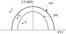
S11043、当至少一个检测电路中存在抵押检测电路当前时刻所处的工作状态位于第一检测电路的性能边界外,且位于安全芯片的性能边界内时,则第一检测电路发出报警信号。S11043: When the current working state of the mortgage detection circuit in at least one detection circuit is outside the performance boundary of the first detection circuit and within the performance boundary of the security chip, the first detection circuit sends an alarm signal.
示例性的,如图11所示,在图11中横轴表示PVT(工艺、电压、温度)平面,纵轴表示安全芯片的时钟频率,坐标系中任意一点表示安全芯片工作时的工作频率和PVT条件。其中,曲线1201表示安全芯片的性能边界,曲线1202表示任意一个检测安全芯片工作状态的电路的性能边界。Exemplarily, as shown in FIG. 11 , in FIG. 11 , the horizontal axis represents the PVT (process, voltage, temperature) plane, the vertical axis represents the clock frequency of the security chip, and any point in the coordinate system represents the operating frequency and PVT conditions. The
第一方面,当安全芯片所处的工作状态处于检测安全芯片工作状态的电路的性能边界内时,即位于如图11中所示的A点时,则表示安全芯片所处的工作条件正常,则该安全芯片中的每个检测安全芯片工作状态电路均不发出报警信号。In the first aspect, when the working state of the security chip is within the performance boundary of the circuit for detecting the working state of the security chip, that is, when it is at point A as shown in Figure 11, it means that the working condition of the security chip is normal. Then each circuit in the security chip for detecting the working state of the security chip will not send out an alarm signal.
第二方面,当安全芯片的工作状态位于曲线1202外且位于曲线1201内时,即如图11所示的B点,虽然安全芯片的所处的工作状态为正常条件,但是检测安全芯片工作状态的电路发出报警信号,这是由于,有可能安全芯片的局部工作状态发生变化,但这种变化并未影响到安全芯片整体的工作状态,因此,只要检测安全芯片工作状态的电路检测到所处的工作状态为非正常工作条件,即发出报警信号。In the second aspect, when the working state of the security chip is located outside the
第三方面,当安全芯片的工作状态处在曲线1201外时,如图11中的C点,此时表明安全芯片可能出错,因此,检测安全芯片工作状态的电路必定会发出报警信号。Thirdly, when the working state of the security chip is outside the
可选的,在步骤S1102之后,本发明实施例提供的方法还包括:Optionally, after step S1102, the method provided by this embodiment of the present invention further includes:
S1105、采取预设保护措施对安全芯片进行复位,以使得安全芯片所存储的数据不泄露。S1105. Take preset protection measures to reset the security chip, so that the data stored in the security chip is not leaked.
示例性的,本发明实施例中的预设保护措施可以为复位整个安全芯片的工作电路(包括CPU电路、加解密电路、随机数生成电路),使得安全信号处于初始状态。其中,该初始状态不包含任何敏感信息,擦除存储体中的所有数据。Exemplarily, the preset protection measure in this embodiment of the present invention may be to reset the working circuit (including the CPU circuit, encryption and decryption circuit, and random number generation circuit) of the entire security chip, so that the security signal is in an initial state. Among them, the initial state does not contain any sensitive information, and all data in the storage body is erased.
以上所述,仅为本发明的具体实施方式,但本发明的保护范围并不局限于此,任何熟悉本技术领域的技术人员在本发明揭露的技术范围内,可轻易想到变化或替换,都应涵盖在本发明的保护范围之内。因此,本发明的保护范围应所述以权利要求的保护范围为准。The above are only specific embodiments of the present invention, but the protection scope of the present invention is not limited thereto. Any person skilled in the art can easily think of changes or substitutions within the technical scope disclosed by the present invention. should be included within the protection scope of the present invention. Therefore, the protection scope of the present invention should be based on the protection scope of the claims.
Claims (19)
Priority Applications (4)
| Application Number | Priority Date | Filing Date | Title |
|---|---|---|---|
| CN201611021892.9ACN108073831B (en) | 2016-11-15 | 2016-11-15 | Method for detecting working state of safety chip and detection circuit |
| PCT/CN2017/086212WO2018090596A1 (en) | 2016-11-15 | 2017-05-26 | Method and circuit for detecting operating condition of security chip |
| US15/814,115US10489595B2 (en) | 2016-11-15 | 2017-11-15 | Method and detection circuit for detecting security chip operating state |
| EP17201774.1AEP3321839A1 (en) | 2016-11-15 | 2017-11-15 | Method and detection circuit for detecting security chip operating state |
Applications Claiming Priority (1)
| Application Number | Priority Date | Filing Date | Title |
|---|---|---|---|
| CN201611021892.9ACN108073831B (en) | 2016-11-15 | 2016-11-15 | Method for detecting working state of safety chip and detection circuit |
Publications (2)
| Publication Number | Publication Date |
|---|---|
| CN108073831A CN108073831A (en) | 2018-05-25 |
| CN108073831Btrue CN108073831B (en) | 2020-07-24 |
Family
ID=60413061
Family Applications (1)
| Application Number | Title | Priority Date | Filing Date |
|---|---|---|---|
| CN201611021892.9AActiveCN108073831B (en) | 2016-11-15 | 2016-11-15 | Method for detecting working state of safety chip and detection circuit |
Country Status (4)
| Country | Link |
|---|---|
| US (1) | US10489595B2 (en) |
| EP (1) | EP3321839A1 (en) |
| CN (1) | CN108073831B (en) |
| WO (1) | WO2018090596A1 (en) |
Families Citing this family (12)
| Publication number | Priority date | Publication date | Assignee | Title |
|---|---|---|---|---|
| CN109144912B (en)* | 2018-09-06 | 2021-09-07 | 晶晨半导体(上海)股份有限公司 | Method and system for acquiring communication interface boundary of storage module |
| US10782346B2 (en) | 2019-01-20 | 2020-09-22 | Texas Instruments Incorporated | Enhanced fault detection of latched data |
| CN111123071A (en)* | 2019-12-19 | 2020-05-08 | 江西智慧云测安全检测中心有限公司 | Single-point laser attack injection testing device for chip safety detection |
| CN114518528B (en)* | 2020-11-19 | 2025-09-05 | 中移物联网有限公司 | A safety chip fault detection circuit and terminal device |
| CN112558923B (en)* | 2020-12-04 | 2023-07-04 | 航天信息股份有限公司 | Method, apparatus, storage medium and device for testing error injection parameters in a random number generator |
| WO2022178793A1 (en)* | 2021-02-26 | 2022-09-01 | 华为技术有限公司 | Delay compensation method and related device |
| CN115840967A (en)* | 2021-09-18 | 2023-03-24 | 紫光同芯微电子有限公司 | Monitoring protection circuit of control signal |
| CN114510397B (en)* | 2022-02-14 | 2025-09-09 | 中广核研究院有限公司 | Current output detection circuit, current output detection method, current output detection device, electronic equipment and storage medium |
| CN114416432B (en)* | 2022-03-29 | 2022-07-08 | 山东云海国创云计算装备产业创新中心有限公司 | Chip safe start detection method, device, equipment and medium |
| CN114722767B (en)* | 2022-05-13 | 2022-09-16 | 紫光同芯微电子有限公司 | Method and device for security chip mixed layout |
| CN115130151B (en)* | 2022-06-06 | 2024-10-29 | 华中科技大学 | Safety detection circuit and safety detection method |
| CN116956365B (en)* | 2023-07-12 | 2025-04-11 | 北京兆讯恒达技术有限公司 | A chip protection circuit for preventing laser light attack and corresponding chip |
Citations (5)
| Publication number | Priority date | Publication date | Assignee | Title |
|---|---|---|---|---|
| CN1971530A (en)* | 2006-12-19 | 2007-05-30 | 威盛电子股份有限公司 | Digital temperature sensing system |
| EP2149886A1 (en)* | 2008-07-30 | 2010-02-03 | STMicroelectronics (Rousset) SAS | Protection of an electronic trigger circuit against fault injections |
| CN102520754A (en)* | 2011-12-28 | 2012-06-27 | 东南大学 | Dynamic voltage scaling system-oriented on-chip monitoring circuit |
| CN103605597A (en)* | 2013-11-20 | 2014-02-26 | 中国科学院数据与通信保护研究教育中心 | Configurable computer protection system and method |
| CN105159374A (en)* | 2015-08-31 | 2015-12-16 | 东南大学 | Online monitoring unit oriented to ultrawide voltage and monitoring window self-adaptive adjusting system |
Family Cites Families (15)
| Publication number | Priority date | Publication date | Assignee | Title |
|---|---|---|---|---|
| JP4680918B2 (en)* | 2003-05-30 | 2011-05-11 | プリヴァリス・インコーポレーテッド | System and method for assignment and use of media content subscription service privileges |
| US7301831B2 (en)* | 2004-09-15 | 2007-11-27 | Rambus Inc. | Memory systems with variable delays for write data signals |
| US20080148343A1 (en)* | 2006-12-19 | 2008-06-19 | International Business Machines Corporation | Debugging security mechanism for soc asic |
| KR100887238B1 (en)* | 2007-08-10 | 2009-03-06 | 삼성전자주식회사 | Dynamic Clock Control System and Method in Pipeline System |
| KR101977733B1 (en)* | 2012-07-12 | 2019-05-13 | 삼성전자주식회사 | Method of detecting fault attack |
| US9607153B2 (en)* | 2013-03-13 | 2017-03-28 | Qualcomm Incorporated | Apparatus and method for detecting clock tampering |
| US9310862B2 (en)* | 2013-05-20 | 2016-04-12 | Advanced Micro Devices, Inc. | Method and apparatus for monitoring performance for secure chip operation |
| US9396360B2 (en)* | 2013-06-27 | 2016-07-19 | Advanced Micro Devices, Inc. | System and method for secure control over performance state |
| US9436844B2 (en)* | 2013-08-29 | 2016-09-06 | Microsoft Technology Licensing, Llc | Access enablement security circuit |
| US9087192B2 (en)* | 2013-09-10 | 2015-07-21 | Infineon Technologies Ag | Electronic circuit and method for monitoring a data processing |
| US9716708B2 (en)* | 2013-09-13 | 2017-07-25 | Microsoft Technology Licensing, Llc | Security certificates for system-on-chip security |
| US10146282B2 (en)* | 2013-10-31 | 2018-12-04 | Advanced Micro Devices, Inc. | System and method for monitoring and controlling a performance state change |
| US20150186676A1 (en)* | 2014-01-01 | 2015-07-02 | Mohit Arora | Real-time clock (rtc) modification detection system |
| EP2960665B1 (en) | 2014-06-27 | 2017-05-24 | Secure-IC SAS | Device and method for calibrating a digital sensor |
| DE102015110144B8 (en)* | 2015-06-24 | 2018-06-28 | Infineon Technologies Ag | Chip and method for testing a processing component of a chip |
- 2016
- 2016-11-15CNCN201611021892.9Apatent/CN108073831B/enactiveActive
- 2017
- 2017-05-26WOPCT/CN2017/086212patent/WO2018090596A1/ennot_activeCeased
- 2017-11-15EPEP17201774.1Apatent/EP3321839A1/ennot_activeWithdrawn
- 2017-11-15USUS15/814,115patent/US10489595B2/enactiveActive
Patent Citations (5)
| Publication number | Priority date | Publication date | Assignee | Title |
|---|---|---|---|---|
| CN1971530A (en)* | 2006-12-19 | 2007-05-30 | 威盛电子股份有限公司 | Digital temperature sensing system |
| EP2149886A1 (en)* | 2008-07-30 | 2010-02-03 | STMicroelectronics (Rousset) SAS | Protection of an electronic trigger circuit against fault injections |
| CN102520754A (en)* | 2011-12-28 | 2012-06-27 | 东南大学 | Dynamic voltage scaling system-oriented on-chip monitoring circuit |
| CN103605597A (en)* | 2013-11-20 | 2014-02-26 | 中国科学院数据与通信保护研究教育中心 | Configurable computer protection system and method |
| CN105159374A (en)* | 2015-08-31 | 2015-12-16 | 东南大学 | Online monitoring unit oriented to ultrawide voltage and monitoring window self-adaptive adjusting system |
Also Published As
| Publication number | Publication date |
|---|---|
| US10489595B2 (en) | 2019-11-26 |
| US20180137283A1 (en) | 2018-05-17 |
| CN108073831A (en) | 2018-05-25 |
| EP3321839A1 (en) | 2018-05-16 |
| WO2018090596A1 (en) | 2018-05-24 |
Similar Documents
| Publication | Publication Date | Title |
|---|---|---|
| CN108073831B (en) | Method for detecting working state of safety chip and detection circuit | |
| KR101312978B1 (en) | Critical-path circuit for performance monitoring | |
| US9303953B2 (en) | Digital system for the detection of variations in operating conditions of an integrated circuit | |
| EP3915034B1 (en) | Alert handling | |
| KR102492252B1 (en) | Voltage-change detection under clock fluctuations | |
| TWI521378B (en) | Apparatus and method for detecting fault injection | |
| CN111095004B (en) | Detection circuit, safety chip and electronic equipment of electromagnetic fault injection | |
| CN103440452B (en) | A kind of chip makes physical integrity detection device | |
| CN103198347A (en) | Secure device anti-tampering circuit | |
| US8466727B2 (en) | Protection against fault injections of an electronic circuit with flip-flops | |
| US9323957B2 (en) | Anti-tamper system based on dual random bits generators for integrated circuits | |
| CN106919764A (en) | The reliability checking method of the ring oscillator physics unclonable function based on FPGA | |
| CN105372577A (en) | On-chip variation detection method and integrated circuit | |
| US9124258B2 (en) | Integrated circuit device, electronic device and method for detecting timing violations within a clock signal | |
| CN109100635B (en) | Circuit and method for integrity detection of multi-channel metal shielded wiring layer | |
| CN114338463B (en) | Safety detection circuit, equipment and detection method based on pulse contraction delay chain | |
| JP2013034133A (en) | Transmission apparatus, transmitting-receiving system, and control method | |
| CN114518528A (en) | Safety chip fault detection circuit and terminal equipment | |
| KR102237747B1 (en) | Semiconductor Apparatus | |
| CN115130151B (en) | Safety detection circuit and safety detection method | |
| US9506983B2 (en) | Chip authentication using scan chains | |
| Anik et al. | Testing and reliability enhancement of security primitives: Methodology and experimental validation | |
| Al-Anwar et al. | Defeating hardware spyware in third party IPs | |
| Giechaskiel et al. | Long-Wire Leakage: The Threat of Crosstalk. | |
| US7574314B2 (en) | Spurious signal detection |
Legal Events
| Date | Code | Title | Description |
|---|---|---|---|
| PB01 | Publication | ||
| PB01 | Publication | ||
| SE01 | Entry into force of request for substantive examination | ||
| SE01 | Entry into force of request for substantive examination | ||
| GR01 | Patent grant | ||
| GR01 | Patent grant |