CN108028280B - Method for manufacturing wound source/drain electrode of contact part of back side metal - Google Patents
Method for manufacturing wound source/drain electrode of contact part of back side metalDownload PDFInfo
- Publication number
- CN108028280B CN108028280BCN201580083367.7ACN201580083367ACN108028280BCN 108028280 BCN108028280 BCN 108028280BCN 201580083367 ACN201580083367 ACN 201580083367ACN 108028280 BCN108028280 BCN 108028280B
- Authority
- CN
- China
- Prior art keywords
- contact
- forming
- fin
- source
- interconnect
- Prior art date
- Legal status (The legal status is an assumption and is not a legal conclusion. Google has not performed a legal analysis and makes no representation as to the accuracy of the status listed.)
- Active
Links
Images


Classifications
- H—ELECTRICITY
- H01—ELECTRIC ELEMENTS
- H01L—SEMICONDUCTOR DEVICES NOT COVERED BY CLASS H10
- H01L23/00—Details of semiconductor or other solid state devices
- H01L23/12—Mountings, e.g. non-detachable insulating substrates
- H01L23/14—Mountings, e.g. non-detachable insulating substrates characterised by the material or its electrical properties
- H01L23/147—Semiconductor insulating substrates
- H—ELECTRICITY
- H01—ELECTRIC ELEMENTS
- H01L—SEMICONDUCTOR DEVICES NOT COVERED BY CLASS H10
- H01L23/00—Details of semiconductor or other solid state devices
- H01L23/28—Encapsulations, e.g. encapsulating layers, coatings, e.g. for protection
- H01L23/31—Encapsulations, e.g. encapsulating layers, coatings, e.g. for protection characterised by the arrangement or shape
- H01L23/3107—Encapsulations, e.g. encapsulating layers, coatings, e.g. for protection characterised by the arrangement or shape the device being completely enclosed
- H—ELECTRICITY
- H01—ELECTRIC ELEMENTS
- H01L—SEMICONDUCTOR DEVICES NOT COVERED BY CLASS H10
- H01L23/00—Details of semiconductor or other solid state devices
- H01L23/48—Arrangements for conducting electric current to or from the solid state body in operation, e.g. leads, terminal arrangements ; Selection of materials therefor
- H01L23/488—Arrangements for conducting electric current to or from the solid state body in operation, e.g. leads, terminal arrangements ; Selection of materials therefor consisting of soldered or bonded constructions
- H01L23/498—Leads, i.e. metallisations or lead-frames on insulating substrates, e.g. chip carriers
- H01L23/49827—Via connections through the substrates, e.g. pins going through the substrate, coaxial cables
- H—ELECTRICITY
- H01—ELECTRIC ELEMENTS
- H01L—SEMICONDUCTOR DEVICES NOT COVERED BY CLASS H10
- H01L24/00—Arrangements for connecting or disconnecting semiconductor or solid-state bodies; Methods or apparatus related thereto
- H—ELECTRICITY
- H01—ELECTRIC ELEMENTS
- H01L—SEMICONDUCTOR DEVICES NOT COVERED BY CLASS H10
- H01L24/00—Arrangements for connecting or disconnecting semiconductor or solid-state bodies; Methods or apparatus related thereto
- H01L24/01—Means for bonding being attached to, or being formed on, the surface to be connected, e.g. chip-to-package, die-attach, "first-level" interconnects; Manufacturing methods related thereto
- H01L24/02—Bonding areas ; Manufacturing methods related thereto
- H01L24/04—Structure, shape, material or disposition of the bonding areas prior to the connecting process
- H01L24/05—Structure, shape, material or disposition of the bonding areas prior to the connecting process of an individual bonding area
- H—ELECTRICITY
- H10—SEMICONDUCTOR DEVICES; ELECTRIC SOLID-STATE DEVICES NOT OTHERWISE PROVIDED FOR
- H10D—INORGANIC ELECTRIC SEMICONDUCTOR DEVICES
- H10D30/00—Field-effect transistors [FET]
- H10D30/60—Insulated-gate field-effect transistors [IGFET]
- H—ELECTRICITY
- H10—SEMICONDUCTOR DEVICES; ELECTRIC SOLID-STATE DEVICES NOT OTHERWISE PROVIDED FOR
- H10D—INORGANIC ELECTRIC SEMICONDUCTOR DEVICES
- H10D30/00—Field-effect transistors [FET]
- H10D30/60—Insulated-gate field-effect transistors [IGFET]
- H10D30/62—Fin field-effect transistors [FinFET]
- H10D30/6219—Fin field-effect transistors [FinFET] characterised by the source or drain electrodes
- H—ELECTRICITY
- H01—ELECTRIC ELEMENTS
- H01L—SEMICONDUCTOR DEVICES NOT COVERED BY CLASS H10
- H01L2224/00—Indexing scheme for arrangements for connecting or disconnecting semiconductor or solid-state bodies and methods related thereto as covered by H01L24/00
- H01L2224/01—Means for bonding being attached to, or being formed on, the surface to be connected, e.g. chip-to-package, die-attach, "first-level" interconnects; Manufacturing methods related thereto
- H01L2224/02—Bonding areas; Manufacturing methods related thereto
- H01L2224/023—Redistribution layers [RDL] for bonding areas
- H01L2224/0237—Disposition of the redistribution layers
- H—ELECTRICITY
- H01—ELECTRIC ELEMENTS
- H01L—SEMICONDUCTOR DEVICES NOT COVERED BY CLASS H10
- H01L2224/00—Indexing scheme for arrangements for connecting or disconnecting semiconductor or solid-state bodies and methods related thereto as covered by H01L24/00
- H01L2224/01—Means for bonding being attached to, or being formed on, the surface to be connected, e.g. chip-to-package, die-attach, "first-level" interconnects; Manufacturing methods related thereto
- H01L2224/02—Bonding areas; Manufacturing methods related thereto
- H01L2224/04—Structure, shape, material or disposition of the bonding areas prior to the connecting process
- H01L2224/04105—Bonding areas formed on an encapsulation of the semiconductor or solid-state body, e.g. bonding areas on chip-scale packages
- H—ELECTRICITY
- H01—ELECTRIC ELEMENTS
- H01L—SEMICONDUCTOR DEVICES NOT COVERED BY CLASS H10
- H01L2224/00—Indexing scheme for arrangements for connecting or disconnecting semiconductor or solid-state bodies and methods related thereto as covered by H01L24/00
- H01L2224/01—Means for bonding being attached to, or being formed on, the surface to be connected, e.g. chip-to-package, die-attach, "first-level" interconnects; Manufacturing methods related thereto
- H01L2224/02—Bonding areas; Manufacturing methods related thereto
- H01L2224/04—Structure, shape, material or disposition of the bonding areas prior to the connecting process
- H01L2224/06—Structure, shape, material or disposition of the bonding areas prior to the connecting process of a plurality of bonding areas
- H01L2224/0601—Structure
- H01L2224/0603—Bonding areas having different sizes, e.g. different heights or widths
- H—ELECTRICITY
- H01—ELECTRIC ELEMENTS
- H01L—SEMICONDUCTOR DEVICES NOT COVERED BY CLASS H10
- H01L2224/00—Indexing scheme for arrangements for connecting or disconnecting semiconductor or solid-state bodies and methods related thereto as covered by H01L24/00
- H01L2224/01—Means for bonding being attached to, or being formed on, the surface to be connected, e.g. chip-to-package, die-attach, "first-level" interconnects; Manufacturing methods related thereto
- H01L2224/10—Bump connectors; Manufacturing methods related thereto
- H01L2224/15—Structure, shape, material or disposition of the bump connectors after the connecting process
- H01L2224/16—Structure, shape, material or disposition of the bump connectors after the connecting process of an individual bump connector
- H01L2224/161—Disposition
- H01L2224/16151—Disposition the bump connector connecting between a semiconductor or solid-state body and an item not being a semiconductor or solid-state body, e.g. chip-to-substrate, chip-to-passive
- H01L2224/16221—Disposition the bump connector connecting between a semiconductor or solid-state body and an item not being a semiconductor or solid-state body, e.g. chip-to-substrate, chip-to-passive the body and the item being stacked
- H01L2224/16225—Disposition the bump connector connecting between a semiconductor or solid-state body and an item not being a semiconductor or solid-state body, e.g. chip-to-substrate, chip-to-passive the body and the item being stacked the item being non-metallic, e.g. insulating substrate with or without metallisation
- H01L2224/16227—Disposition the bump connector connecting between a semiconductor or solid-state body and an item not being a semiconductor or solid-state body, e.g. chip-to-substrate, chip-to-passive the body and the item being stacked the item being non-metallic, e.g. insulating substrate with or without metallisation the bump connector connecting to a bond pad of the item
- H—ELECTRICITY
- H01—ELECTRIC ELEMENTS
- H01L—SEMICONDUCTOR DEVICES NOT COVERED BY CLASS H10
- H01L23/00—Details of semiconductor or other solid state devices
- H01L23/12—Mountings, e.g. non-detachable insulating substrates
- H01L23/14—Mountings, e.g. non-detachable insulating substrates characterised by the material or its electrical properties
- H01L23/145—Organic substrates, e.g. plastic
- H—ELECTRICITY
- H01—ELECTRIC ELEMENTS
- H01L—SEMICONDUCTOR DEVICES NOT COVERED BY CLASS H10
- H01L23/00—Details of semiconductor or other solid state devices
- H01L23/12—Mountings, e.g. non-detachable insulating substrates
- H01L23/14—Mountings, e.g. non-detachable insulating substrates characterised by the material or its electrical properties
- H01L23/15—Ceramic or glass substrates
Landscapes
- Engineering & Computer Science (AREA)
- Computer Hardware Design (AREA)
- Microelectronics & Electronic Packaging (AREA)
- Power Engineering (AREA)
- Physics & Mathematics (AREA)
- Condensed Matter Physics & Semiconductors (AREA)
- General Physics & Mathematics (AREA)
- Metal-Oxide And Bipolar Metal-Oxide Semiconductor Integrated Circuits (AREA)
- Thin Film Transistor (AREA)
- Insulated Gate Type Field-Effect Transistor (AREA)
- Electrodes Of Semiconductors (AREA)
Abstract
Translated fromChinese
Description
Translated fromChinese技术领域technical field
半导体器件包含具有来自器件背侧的电连接的器件。Semiconductor devices include devices with electrical connections from the backside of the device.
背景技术Background technique
过去几十年,集成电路中的特征的缩放已经成为日益增长的半导体行业背后的驱动力。缩放到越来越小的特征实现在半导体芯片的有限基板面上的功能单元的增加密度。例如,缩小晶体管大小允许在芯片上结合增加数量的存储器器件,从而引起具有增加的容量的产品的制造。但是,对于更多的容量的驱动并不是没有问题的。用来优化每个器件的性能的必要性变得日益显著。The scaling offeatures in integrated circuits has been the driving force behind the growing semiconductor industry over the past few decades. Scaling to smaller and smaller features enables an increased density of functional units on the limited real estate of a semiconductor chip. For example, shrinking transistor size allows for the incorporation of increased numbers of memory devices on a chip, leading to the manufacture of products with increased capacity. However, drives for more capacity are not without problems. The need to optimize the performance of each device is becoming increasingly evident.
诸如中央处理单元器件的未来电路器件将预期在单个管芯(dye)或芯片中集成的高性能器件和低电容、低功率器件。Future circuit devices such as central processing unit devices will anticipate high performance devices and low capacitance, low power devices integrated in a single die or chip.
附图说明Description of drawings
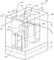
图1示出位于衬底上的三维晶体管器件的一部分的顶部侧透视图,其是例如晶圆上的集成电路管芯或芯片的一部分。Figure 1 shows a top side perspective view of a portion of a three-dimensional transistor device on a substrate, eg, a portion of an integrated circuit die or chip on a wafer.
图2示出在形成到晶体管器件的接触部开口或通孔之后的图1的结构。FIG. 2 shows the structure of FIG. 1 after forming contact openings or vias to transistor devices.
图3A-3C示出经过图2的结构的横截面侧视图。3A-3C show cross-sectional side views through the structure of FIG. 2 .
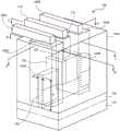
图4示出在形成到三维晶体管器件结构的接触部和互连之后的图2的结构。FIG. 4 shows the structure of FIG. 2 after forming contacts and interconnects to the three-dimensional transistor device structure.
图5A-5C示出经过图4的结构的横截面侧视图。5A-5C show cross-sectional side views through the structure of FIG. 4 .
图6A-6C示出在倒置或倒装该结构并将该结构连接到载体之后的图5A-5C的结构。Figures 6A-6C show the structure of Figures 5A-5C after inverting or flipping the structure and attaching the structure to a carrier.
图7A-7C示出在去除或变薄衬底以便暴露器件的鳍的第二侧或背侧之后的图6A-6C的结构。7A-7C illustrate the structure of FIGS. 6A-6C after the substrate has been removed or thinned to expose the second or backside of the fins of the device.
图8A-8C示出在晶体管器件的背侧上沉积电介质材料之后的图7A-7C的结构。8A-8C illustrate the structure of FIGS. 7A-7C after deposition of a dielectric material on the backside of the transistor device.
图9A-9C示出在将晶体管器件的背侧上的电介质材料进行图案化之后的图8A-8C的结构。9A-9C illustrate the structure of FIGS. 8A-8C after patterning the dielectric material on the backside of the transistor device.
图10A-10C示出在利用传导接触材料填充电介质材料中的通孔开口之后的图9A-9C的结构,并示出连接到源极接触部以作为第一背侧互连或金属层的一部分的互连。Figures 10A-10C show the structure of Figures 9A-9C after filling the via opening in the dielectric material with conductive contact material and showing the connection to the source contact as part of the first backside interconnect or metal layer interconnection.
图11示出经过在源极区域中只在鳍的一侧上具有从器件层次(stratum)的第一侧延伸到器件层次的第二侧的接触部的三维晶体管器件的源极区域的横截面的代表性示例。Figure 11 shows a cross-section through the source region of a three-dimensional transistor device with contacts extending from a first side of the device stratum to a second side of the device stratum on only one side of the fin in the source region A representative example of .
图12示出包含连接到封装衬底的集成电路芯片或管芯的组合件的一个实施例的横截面示意性侧视图。Figure 12 shows a cross-sectional schematic side view of one embodiment of an assembly comprising an integrated circuit chip or die connected to a packaging substrate.
图13是用来形成到连接到背侧金属化部的三维晶体管器件的源极和漏极的卷绕接触部的工艺的流程图。13 is a flowchart of a process for forming wraparound contacts to the source and drain of a three-dimensional transistor device connected to backside metallization.
图14是实现一个或多个实施例的内插器。Figure 14 is an interposer implementing one or more embodiments.
图15图示计算器件的实施例。Figure 15 illustrates an embodiment of a computing device.
具体实施方式Detailed ways
本文中描述的实施例涉及半导体器件,其包含在器件的背侧下方或在其上具有互连或接线的非平面半导体器件(例如,三维器件)。这样的实施例通过利用背侧显露和背侧处理来实现。描述的实施例包含一种设备,该设备包含:电路结构,其包括第一侧和相反的第二侧,第一侧包含器件层,其包含多个器件;耦合到第一侧上的多个器件中的一个的导电接触部;以及部署在第二侧上并连接到传导接触部的导电互连。还描述形成这样的器件的实施例。背侧显露处理允许在能够制造的连接的类型中的灵活性。Embodiments described herein relate to semiconductor devices, including non-planar semiconductor devices (eg, three-dimensional devices) with interconnects or wires under or on the backside of the device. Such embodiments are achieved by utilizing backside exposure and backside processing. The described embodiments include an apparatus comprising: a circuit structure comprising a first side and an opposite second side, the first side comprising a device layer comprising a plurality of devices; a plurality of devices coupled to the first side a conductive contact of one of the devices; and a conductive interconnect disposed on the second side and connected to the conductive contact. Embodiments of forming such devices are also described. The backside exposed process allows flexibility in the types of connections that can be made.
图1-10C描述形成三维或非平面半导体器件的方法或工艺,该三维或非平面半导体器件包含在该结构的非器件侧或背侧上的电连接。在一个实施例中,器件是三维金属氧化物半导体场效应晶体管(MOSFET),并且它是隔离器件,或者是多个嵌套式器件中的一个器件。如将领会,对于典型的集成电路,可在单个衬底上制造N-沟道和P-沟道晶体管以便形成互补金属氧化物半导体(CMOS)集成电路。此外,可制造附加互连以便将这些器件集成到集成电路中。1-10C describe a method or process of forming a three-dimensional or non-planar semiconductor device that includes electrical connections on the non-device or backside of the structure. In one embodiment, the device is a three-dimensional Metal Oxide Semiconductor Field Effect Transistor (MOSFET), and it is an isolated device, or one of a plurality of nested devices. As will be appreciated, for a typical integrated circuit, N-channel and P-channel transistors may be fabricated on a single substrate to form a complementary metal-oxide-semiconductor (CMOS) integrated circuit. Additionally, additional interconnects can be fabricated to integrate these devices into integrated circuits.
在制造诸如多栅极晶体管和FinFET的非平面晶体管中,可利用非平面半导体本体来形成通常具有在相对小的栅极长度(例如,小于约30 nm)的情况下完全耗尽的能力的晶体管。这些半导体本体通常是鳍形的,并且因此通常称为晶体管“鳍”。例如,在三栅极晶体管中,晶体管鳍具有在块体半导体衬底或绝缘体上硅衬底上形成的顶部表面和两个相反侧壁。可在半导体本体的顶部表面或上表面和侧壁上形成栅极电介质,并且可在半导体本体的顶部表面或上表面上的栅极电介质之上以及在与半导体本体的侧壁上的栅极电介质相邻地形成栅极电极。由于栅极电介质和栅极电极与半导体本体的三个表面相邻,所以形成三个单独的沟道和栅极。由于存在形成的三个单独沟道,所以当晶体管接通时,能够完全耗尽半导体本体。关于finFET晶体管,栅极材料和电极接触半导体本体的侧壁,使得形成两个单独沟道。In the fabrication of non-planar transistors such as multi-gate transistors and FinFETs, non-planar semiconductor bodies can be exploited to form transistors that typically have the ability to be fully depleted at relatively small gate lengths (e.g., less than about 30 nm) . These semiconductor bodies are usually fin-shaped and are therefore often referred to as transistor "fins". For example, in a tri-gate transistor, the transistor fin has a top surface and two opposing sidewalls formed on a bulk semiconductor substrate or a silicon-on-insulator substrate. A gate dielectric may be formed on the top or upper surface and sidewalls of the semiconductor body, and may be over the gate dielectric on the top or upper surface of the semiconductor body and on the sidewalls of the semiconductor body A gate electrode is formed adjacently. Since the gate dielectric and gate electrode are adjacent to three surfaces of the semiconductor body, three separate channels and gates are formed. Due to the presence of three separate channels formed, the semiconductor body can be completely depleted when the transistor is switched on. With regard to finFET transistors, the gate material and electrodes contact the sidewalls of the semiconductor body such that two separate channels are formed.
图1示出半导体或绝缘体上半导体(SOI)衬底的一部分的顶部侧透视图,其是例如晶圆上的集成电路管芯或芯片的一部分。特别地,图1示出包含硅或SOI的衬底110的结构100。重叠衬底110的是可选的缓冲层120。在一个实施例中,缓冲层是在一个实施例中通过生长技术在衬底110上引入的硅锗缓冲层。代表性地,缓冲层120具有大约几百纳米(nm)的代表性厚度。FIG. 1 shows a top side perspective view of a portion of a semiconductor or semiconductor-on-insulator (SOI) substrate, eg, a portion of an integrated circuit die or chip on a wafer. In particular, FIG. 1 shows a
在图1所图示的实施例中部署在可选缓冲层120和衬底110的表面(如所看到的上表面)是诸如N-型晶体管器件或P-型晶体管器件的晶体管器件的一部分。在该实施例中与N-型或P-型晶体管器件共有的是部署在缓冲层120的表面上的本体或鳍130。在一个实施例中,鳍130由诸如硅、硅锗或III-V族或IV-V族半导体材料的半导体材料形成。在一个实施例中,根据用于形成三维集成电路器件的常规处理技术来形成鳍130的材料。代表性地,在衬底上外延生长半导体材料,并然后将它形成为鳍130(例如,通过掩蔽和蚀刻工艺)。Disposed on the
在一个实施例中,鳍130具有大于高度尺寸H的长度尺寸L。代表性的长度范围约为10纳米(nm)到1毫米(mm),并且代表性的高度范围约为5 nm到200 nm。鳍130也具有代表性约为4-10 nm的宽度W。如所图示,鳍130是从衬底110的表面或在衬底110的表面上(或者可选地从缓冲层120或在缓冲层120上)延伸的三维本体。如图1所图示的三维本体是从如所看到的缓冲层120的表面突出的具有相反侧(第一侧和第二侧)的长方形本体。领会的是,在处理这样的本体时,利用可用的加工工具(tooling),真正长方形的外形可能是不可实现的,而是可能导致其它形状。代表性形状包含但不限于梯形形状(例如,底部比顶部宽)和弓形形状。In one embodiment,
在图1的结构的实施例中部署在鳍130上的是栅极堆。在一个实施例中,栅极堆包含例如二氧化硅或具有大于二氧化硅的电介质常数的电介质材料(高k电介质材料)的栅极电介质层。在一个实施例中,部署在栅极电介质层上的是例如金属的栅极125。栅极堆可包含位于其相反侧上的电介质材料的间隔器150。间隔器150的代表性材料是诸如氮化硅(SiN)或碳氮化硅(SiCN)的低k材料。图1示出位于鳍130上以及与栅极堆的侧壁相邻的间隔器150。在鳍130上或在其中在栅极堆的相反侧上形成的是结区域(源极140A和漏极140B)。Disposed on the
在一个实施例中,为了形成三维晶体管结构,例如通过毯覆式沉积(blanketdeposition),后跟牺牲或虚拟栅极材料的毯覆式沉积而在鳍130上形成栅极电介质材料。在该结构之上引入掩模材料,并将其进行图案化以便保护指定沟道区域之上的栅极堆材料(具有牺牲或虚拟栅极材料的栅极堆)。然后,利用蚀刻工艺来去除不预期区中的栅极堆材料,并对指定沟道区域之上的栅极堆进行图案化。然后,形成间隔器150。用来形成间隔器150的一种技术是要在该结构上沉积膜,保护预期区中的膜,并接着进行蚀刻以便将膜图案化为预期的间隔器尺寸。In one embodiment, to form the three-dimensional transistor structure, a gate dielectric material is formed on the
在鳍130和间隔器150上形成包含牺牲或虚拟栅极材料的栅极堆之后,在鳍130上或在其中形成结区域(源极和漏极)。在鳍130中在栅极堆(栅极电介质上的牺牲栅极电极)的相反侧上形成源极和漏极。在图1中所示的实施例中,通过外延生长源极和漏极材料以作为鳍130的一部分上的包层来形成源极140A和漏极140B。源极140A和漏极140B的代表性材料包含但不限于硅、硅锗、或III-V族或IV-V族化合物半导体材料。备选地,可通过去除鳍材料的部分并在去除鳍材料的指定结区域中外延生长源极和漏极材料来形成源极140A和漏极140B。After forming a gate stack including sacrificial or dummy gate material on
在一个实施例中,在形成源极140A和漏极140B之后,去除牺牲或虚拟栅极,并利用栅极电极材料代替。在一个实施例中,在去除牺牲或虚拟栅极堆之前,在该结构上沉积电介质材料。在一个实施例中,电介质材料是二氧化硅或低k电介质材料,其作为覆盖层沉积并接着抛光以便暴露牺牲或虚拟栅极125。然后,通过例如蚀刻工艺去除牺牲或虚拟栅极和栅极电介质。In one embodiment, after the
在去除牺牲或虚拟栅极和栅极电介质之后,在栅极电极区域中形成栅极堆。在包含栅极电介质和栅极电极的结构上引入(例如,沉积)栅极堆。在实施例中,栅极电极堆的栅极电极125由金属栅极组成,并且栅极电介质层由具有大于二氧化硅的电介质常数的电介质常数的材料(高k材料)组成。例如,在一个实施例中,栅极电介质层127(见图3C)由诸如但不限于氧化铪、氧氮化铪、硅酸铪、氧化镧、氧化锆、硅酸锆、氧化钽、钛酸钡锶、钛酸钡、钛酸锶、氧化钇、氧化铝、氧化 铅钪钽、铌酸锌铅或其组合的材料组成。在一个实施例中,栅极电极125由诸如但不限于金属氮化物、金属碳化物、金属硅化物、金属铝化物、铪、锆、钛、钽、铝、钌、钯、铂、钴、镍或传导金属氧化物的金属层组成。在形成栅极堆之后,在三维晶体管器件上(例如,在ILD0上)沉积二氧化硅或低k电介质材料的附加电介质材料,以便将器件结构包封或嵌入在电介质材料中。图1示出包封三维晶体管器件(例如,作为ILD0)的电介质材料155A。After removal of the sacrificial or dummy gate and gate dielectric, a gate stack is formed in the gate electrode region. A gate stack is introduced (eg, deposited) on a structure including a gate dielectric and a gate electrode. In an embodiment, the
图2示出在形成经过电介质材料的开口或通孔以便暴露源极140A和漏极140B之后的图1的结构。在一个实施例中,通过光刻工艺,例如通过掩蔽电介质材料的(如所看到的)顶部表面的区以便限定开口的区并利用相对于源极140A和漏极140B的材料对于电介质材料具选择性的蚀刻剂经过电介质材料155A蚀刻开口或通孔,来形成围绕源极区域的开口145A和围绕漏极区域的开口145B。如图2图示,在一个实施例中,蚀刻区足够大以便以分别暴露源极140A和漏极140B的顶部表面以及源极和漏极的相反侧表面的方式形成开口145A和开口145B。在一个实施例中,蚀刻是各向异性蚀刻,其进行至超过相应源极和漏极的深度的深度。由于在该实施例中,作为在鳍130的顶部表面和侧壁表面上的包层而形成源极140A和漏极140B,所以源极和漏极将在蚀刻经过电介质材料155A进行超过源极140A和漏极140B时充当掩模,以便分别直接在源极140A和漏极140B下方的鳍130的相反侧壁上和与其相邻地留下电介质材料。在一个实施例中,蚀刻经过电介质材料155A进行至鳍130的底部附近的深度。除了源极区域中的开口145A和漏极区域中的开口145B之外,图2还示出经过电介质材料155A到栅极电极125形成的通孔或开口128。开口128可通过与开口145A和145B类似的掩模和蚀刻工艺形成,并且在该实施例中,它暴露栅极电极125的顶部的一部分。FIG. 2 shows the structure of FIG. 1 after forming openings or vias through the dielectric material to expose
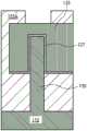
图3A-3C示出经过图2的横截面侧视图。更特别地,图3A示出经过图2的线A-A’的横截面侧视图,其是经过鳍130的横截面;图3B示出经过线B-B’的横截面,其是经过源极140A的横截面;并且图3C示出经过线C-C’的横截面,其是经过栅极电极125的横截面。本描述通篇中将呈现相同定向的横截面(A-C)。图3B示出暴露源极140A的顶部表面和相反侧表面并进行至鳍130的底部附近的深度的开口或通孔145A,所述图3C示出到栅极电极125的开口。3A-3C show cross-sectional side views through FIG. 2 . More particularly, FIG. 3A shows a cross-sectional side view through line AA' of FIG. 2, which is a cross-section through
图4示出在形成到三维晶体管器件结构的接触部和互连之后的图1的结构。在该实施例中,进行电连接以作为到源极140A、漏极140B和栅极电极125的第一互连层或金属层。代表性地,为了形成到源极140A、漏极140B和栅极电极125的个别电接触部,在开口128、145A和145B中引入(例如,沉积)例如钨的接触材料,并填充开口以便形成到源极140A的接触部165A、到漏极140B的接触部165B和到栅极电极125的接触部175。然后,可以利用传导籽晶材料播种电介质材料155的表面(如所看到的顶部表面),并接着利用掩蔽材料进行图案化以便为互连路径限定开口,其中相应开口暴露接触部165A、接触部165B和接触部175。然后,通过电镀工艺引入诸如铜的传导材料,以便形成连接到至源极140A的接触部165A的互连160A、连接到接触部165B的互连160B和连接到栅极电极125的接触部175的互连170。接着,能够去除掩蔽材料和不想要的籽晶材料。在形成互连以作为初始金属层之后,可沉积例如二氧化硅或低k电介质材料的电介质材料以作为互连上和在其周围的ILD1层。然后,可根据常规工艺形成附加互连层。FIG. 4 shows the structure of FIG. 1 after forming contacts and interconnects to the three-dimensional transistor device structure. In this embodiment, electrical connections are made as a first interconnect layer or metal layer to source 140A, drain 140B, and
图5A-5C示出经过图4的结构的横截面侧视图。特别地,图5A示出通过经过鳍130的线A-A’的横截面;图5B示出通过经过漏极140B的线B-B’的横截面;并且图5C示出通过经过栅极电极125的线C-C’的横截面侧视图。参考图5B,该图示出连接到源极140A的顶部表面(如所看到的)并具有接触源极140A的相应相反侧壁并越过源极140A朝向鳍130的底部延伸的突出部分1651A和突出部分1652A的接触部165A。5A-5C show cross-sectional side views through the structure of FIG. 4 . In particular, FIG. 5A shows a cross-section through the line AA' passing through the
图6A-6C示出在在该结构的器件侧上的互连上引入(例如,沉积)电介质材料,并且倒置或倒装该结构并将该结构连接到载体之后的图5A-5C的结构。图6A-6C分别表示经过鳍130、漏极140B和栅极电极125的横截面,如上文关于图3A-3C和图5A-5C所描述。参考图6A-6C,在该实施例中,沉积例如二氧化硅或低k电介质材料的电介质材料155B以作为ILD1层。然后,倒装结构100,并在器件侧处将它连接到载体180(器件侧向下)。载体180是例如半导体晶圆。可在电介质材料155B和载体180之间通过粘合剂或其它接合技术将结构100连接到载体180。6A-6C illustrate the structure of FIGS. 5A-5C after introducing (eg, depositing) a dielectric material over the interconnects on the device side of the structure, and inverting or flip-chipping the structure and connecting the structure to a carrier. 6A-6C represent cross-sections through
图7A-7C示出在去除或变薄衬底110以便暴露鳍130的第二侧或背侧之后的图6A-6C的结构。在一个实施例中,可通过诸如机械研磨或蚀刻工艺的变薄工艺来去除衬底110。图7A-7C示出从结构的第二侧或背侧暴露的鳍130。在暴露鳍130之后,可以可选地使鳍凹陷。图7A-7C还示出在使鳍130凹陷之后的结构。在一个实施例中,为了使鳍130凹陷,蚀刻工艺可以与相对于电介质材料155A对鳍材料的去除具选择性的蚀刻剂一起被利用。备选地,可在具有暴露鳍130的开口的电介质材料155的表面(暴露的背侧表面)上对掩蔽材料进行图案化。可通过例如蚀刻工艺来去除鳍130的材料以便使鳍130凹陷并接着去除掩蔽材料。7A-7C illustrate the structure of FIGS. 6A-6C after
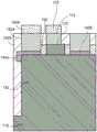
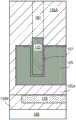
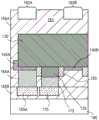
图8A-8C示出在鳍130的背侧上沉积电介质材料之后的图7A-7C的结构。图8A-8C示出通过例如毯覆式沉积工艺沉积的例如二氧化硅或低K电介质材料的电介质材料181。图9A-9C示出在将电介质材料181进行图案化以便在源极和漏极区域中形成接触部开口之后的图8A-8C的结构。可通过例如在具有与例如鳍130的相反侧上的源极和漏极区域相反的开口或通孔的电介质材料181的表面上形成掩蔽材料来将电介质材料181图案化。图9A示出经过电介质材料181的对应于鳍的源极区域(源极140A)的鳍130的背侧上定向的开口182A以及经过电介质材料181的对应于鳍的漏极区域(漏极140B)的开口182B。图9B示出,开口(例如,开口182A)具有大于鳍130的宽度尺寸的直径的尺寸,并暴露接触部165A的突出部分1651A和突出部分1652A的端。8A-8C illustrate the structure of FIGS. 7A-7C after deposition of a dielectric material on the backside of the
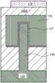
图10A-10C示出在利用诸如钨的传导接触材料填充电介质材料181中的通孔开口之后的图9A-9C的结构。图10A示出与源极140A相关联的接触部190A和与漏极140B相关联的接触金属190B。图10B示出连接到接触部165A的突出部分1651A和突出部分1652A的接触金属190A。图10B示出分别从结构的相反侧(第一侧或器件侧与背侧或第二侧)(经由接触材料)到源极140A的连接。现在可通过例如上文关于器件侧互连(见图4和5A-5C以及随附文本)描述的技术形成到接触部190A和190B的互连。图10A-10C示出连接到至源极140A的接触部190A的互连195A以作为例如第一背侧互连或金属层的一部分。图10A-10C还示出在互连或金属层上沉积二氧化硅或低k电介质材料的电介质材料155C之后的结构。10A-10C illustrate the structure of FIGS. 9A-9C after filling the via opening in
在上文参考图1-10C描述的结构的实施例中,示出背侧金属接触部分别在源极和漏极中围绕鳍的相反侧缠绕。在另一个实施例中,可分别在源极和漏极区域中只沿鳍的一侧形成金属接触部。图11示出经过在源极区域中只在鳍的一侧上具有从器件层次的第一侧延伸到器件层次的第二侧的接触部的三维晶体管器件的源极区域的横截面的代表性示例。所利用的参考数字与图10B中相同。用来形成图11中示出的结构的工艺将与图1-10C中示出的工艺类似,其中仅开口通过例如光刻工艺在电介质材料中形成以便暴露结(源极140A)(见图2以及随附文本)。而且,接触金属190A能够具有更小宽度,因为它并非必需例如跨鳍的宽度延伸。In the embodiments of the structures described above with reference to FIGS. 1-10C , the backside metal contacts are shown wrapping around opposite sides of the fin in the source and drain, respectively. In another embodiment, metal contacts may be formed along only one side of the fin in the source and drain regions, respectively. Figure 11 shows a representation of a cross-section through a source region of a three-dimensional transistor device having contacts extending from a first side of the device level to a second side of the device level on only one side of the fin in the source region example. The reference numerals utilized are the same as in Fig. 10B. The process used to form the structure shown in FIG. 11 will be similar to that shown in FIGS. 1-10C , where only openings are formed in the dielectric material by, for example, a photolithographic process to expose the junction (
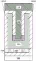
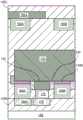
图12示出包含连接到封装衬底的集成电路芯片或管芯的组合件的一个实施例的横截面示意性侧视图。组合件200包含可如上文参考图1-11描述地那样形成的管芯210。管芯210包含器件层或层次215,其包含多个器件(例如,晶体管器件)。器件层次215包含代表该层次的第一侧的第一侧2150A和与第一侧2150A相反的第二侧或背侧2150B。晶体管器件包含例如一个或多个功率晶体管和逻辑电路系统。连接到第一侧上的管芯210的器件层次215的是互连220,在一个实施例中,互连220包含但不限于从第一侧2150A连接到器件层次215的器件的多个传导金属线。参考图1-11,互连160A、互连160B和互连170(见图4)代表位于器件层次215上方的第一级互连220。如所看到的,部署在互连220上方的是与上文参考图6A-11描述的载体衬底180类似的载体衬底240。在该实施例中,经过管芯的第二侧2100B连接到管芯210的器件的是互连230,互连230可以是例如功率互连(VDD、VDD-门控和VSS)、逻辑互连或两者。第二侧或背侧2100B上的互连230包含金属化部的一个或多个级或行。参考图10A-11,互连195A代表位于器件层次215下方的第一级互连230。图12还示出,金属化部的这样的级中的级连接到接触点(例如,C4凸点(bump))250,接触点250可操作以便将管芯210连接到封装290。图12还示出经过封装衬底290到管芯210的VDD和VSS连接。Figure 12 shows a cross-sectional schematic side view of one embodiment of an assembly comprising an integrated circuit chip or die connected to a packaging substrate.
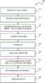
图13是用来形成到连接到背侧金属化部的三维晶体管器件的源极和漏极的卷绕接触部的工艺的流程图。参考图11,工艺300从在基体衬底(base substrate)上形成三维晶体管器件开始,该器件包含从基体衬底延伸的鳍以及在鳍中或在其上形成的源极和漏极(方框310)。从该结构的第一侧或器件侧,围绕器件的源极和漏极区域形成深通孔或开口(方框315)。利用接触材料填充通孔或开口以便形成卷绕接触部,并构建器件侧金属化部(方框320)。在构建金属化部之后,器件被倒装并器件侧向下接合到载体(方框325)。接着,去除基体衬底以便暴露鳍(方框330),并可选地使鳍凹陷(方框335)。然后,在具有到卷绕接触部的通孔或开口的器件的背侧上引入电介质材料并进行图案化(方框340)。利用接触材料填充背侧通孔或开口以便制作到卷绕接触部的背侧接触部(方框345)。接着,可选地构建背侧金属化部(方框350)。13 is a flowchart of a process for forming wraparound contacts to the source and drain of a three-dimensional transistor device connected to backside metallization. Referring to FIG. 11 ,
参考三维晶体管器件(例如,多栅极器件)描述了以上实施例。在另一个实施例中,本文中提出的描述能够适用于其它器件,例如平面器件或纳米线器件。The above embodiments are described with reference to three-dimensional transistor devices (eg, multi-gate devices). In another embodiment, the description presented herein can be applied to other devices, such as planar devices or nanowire devices.
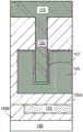
图14图示包含一个或多个实施例的内插器400。内插器400是用来将第一衬底402桥接到第二衬底404的中介衬底。第一衬底402可以是例如集成电路管芯。第二衬底404可以是例如存储器模块、计算机母板或另一个集成电路管芯。一般来说,内插器400的目的是要将连接伸展到更宽间距或将连接重新布线至不同连接。例如,内插器400可将集成电路管芯耦合到球栅阵列(BGA)406,BGA 406能够随后耦合到第二衬底404。在一些实施例中,第一和第二衬底402/404附连到内插器400的相反侧。在其它实施例中,第一和第二衬底402/404附连到内插器400的相同侧。在进一步实施例中,通过内插器400互连三个或更多个衬底。Figure 14 illustrates an
内插器400可由环氧树脂、玻璃纤维增强环氧树脂、陶瓷材料或诸如聚酰亚胺的聚合物材料形成。在进一步实现中,内插器可由备选的刚性或柔性材料形成,其可包含上文供在半导体衬底中使用描述的相同材料,诸如硅、锗以及其它III-V族和IV族材料。
内插器可包含金属互连408和通孔410,包含但不限于穿硅通孔(TSV)412。内插器400还可包含嵌入式器件414,包含无源和有源器件。这样的器件包含但不限于电容器、解耦电容器、电阻器、电感器、保险丝、二极管、变压器、传感器和静电放电(ESD)器件。还可在内插器400上形成更复杂的器件,诸如射频(RF)器件、功率放大器、功率管理器件、天线、阵列、传感器和MEMS器件。The interposer may include
根据实施例,可在制造内插器400中使用本文中公开的设备或工艺。According to an embodiment, an apparatus or process disclosed herein may be used in fabricating
图15图示根据一个实施例的计算器件500。计算器件500可包含多个组件。在一个实施例中,这些组件附连到一个或多个母板。在备选实施例中,将这些组件制造到单个芯片上系统(SoC)管芯而不是母板上。计算器件500中的组件包含但不限于集成电路管芯502和至少一个通信芯片508。在一些实现中,作为集成电路管芯502的一部分制造通信芯片508。集成电路管芯502可包含CPU 504以及管芯上存储器506(通常用作高速缓冲存储器),其能够通过诸如嵌入式DRAM(eDRAM)或自旋转移扭矩存储器(STTM或STTM-RAM)的技术提供。FIG. 15 illustrates a
计算器件500可包含其它组件,其可以或者可以不在物理上和电气上耦合到母板或在SoC管芯内制造。这些其它组件包含但不限于易失性存储器510(例如,DRAM)、非易失性存储器512(例如,ROM或闪速存储器)、图形处理单元514(GPU)、数字信号处理器516、加密处理器542(在硬件内运行加密算法的专业化处理器)、芯片组520、天线522、显示器或触摸屏显示器524、触摸屏控制器526、电池528或其它功率源、功率放大器(未示出)、全球定位系统(GPS)器件544、指南针530、运动协处理器或传感器532(其可包含加速度计、陀螺仪和指南针)、扬声器534、相机536、用户输入器件538(例如键盘、鼠标、触控笔和触板)和大容量存储器件540(例如硬盘驱动、致密盘(CD)、数字通用盘(DVD)等)。
通信芯片508实现用于数据来往于计算器件500的传递的无限通信。术语“无线”和它的衍生词可用来描述可通过使用通过非固态媒介的调制电磁辐射来传达数据的电路、器件、系统、方法、技术、通信信道等。术语并不暗示关联的器件不包含任何线,但在一些实施例中它们可不包括任何线。通信芯片508可以实现许多无线标准或协议中的任何,其包含但不限于Wi-Fi(IEEE 802.11系列)、WiMAX(IEEE 802.16系列)、IEEE 802.20、长期演进(LTE)、Ev-DO、HSPA+、HSDPA+、HSUPA+、EDGE、GSM、GPRS、CDMA、TDMA、DECT、蓝牙、其衍生物,以及指定为3G、4G、5G及以后的任何其他无线协议。计算器件500可包含多个通信芯片508。例如,第一通信芯片508可专用于诸如Wi-Fi和蓝牙的较短程无线通信,并且第二通信芯片508可专用于诸如GPS、EDGE、GPRS、CDMA、WiMAX、LTE、Ev-DO等的较长程无线通信。
计算器件500的处理器504包含根据上文描述的实施例形成有卷绕接触部和可选的背侧金属化部的诸如晶体管或金属互连的一个或多个器件。术语“处理器”可以指对来自寄存器和/或存储器的电子数据进行处理以便将那个电子数据变换为可存储在寄存器和/或存储器中的其它电子数据的任何器件或器件的一部分。
通信芯片508也可包含根据上文描述的实施例形成有卷绕接触部和可选的背侧金属化部的诸如晶体管或金属互连的一个或多个器件。The
在进一步实施例中,容纳在计算器件500内的另一个组件可包含根据上文描述的实现形成有卷绕接触部和可选的背侧金属化部的诸如晶体管或金属互连的一个或多个器件。In a further embodiment, another component housed within
在各种实施例中,计算器件500可以是膝上型计算机、上网本计算机、笔记本计算机、超级本计算机、智能电话、平板、个人数字助理(PDA)、超级移动PC、移动电话、桌上型计算机、服务器、打印机、扫描仪、监测器、机顶盒、娱乐控制单元、数码相机、便携式音乐播放器或数字视频记录器。在进一步实现中,计算器件500可以是处理数据的任何其它电子器件。In various embodiments,
示例example
示例1是一种设备,其包含:电路结构,其包含第一侧和相反的第二侧,第一侧包含器件层,其多个器件;耦合到第一侧上的多个器件中的一个的导电接触部;以及部署在结构的第二侧上并耦合到传导接触部的导电互连。Example 1 is an apparatus comprising: a circuit structure comprising a first side and an opposite second side, the first side comprising a device layer, a plurality of devices thereof; one of the plurality of devices coupled to the first side and a conductive interconnect disposed on the second side of the structure and coupled to the conductive contact.
在示例2中,示例1的设备的器件包括包含第一侧壁和相反的第二侧壁的本体,其中传导接触部部署在第一侧壁和第二侧壁的每个侧壁上。In Example 2, the device of Example 1 includes a body comprising a first sidewall and an opposite second sidewall, wherein the conductive contact is disposed on each of the first and second sidewalls.
在示例3中,示例2的设备的接触部包含部署在器件的第一侧壁上的第一部分和部署在第二侧壁上的第二部分,其中第一部分和第二部分中的每个在结构的第二侧的方向上从器件单独延伸。In Example 3, the contact portion of the device of Example 2 comprises a first portion disposed on a first sidewall of the device and a second portion disposed on a second sidewall, wherein each of the first portion and the second portion is positioned at The direction of the second side of the structure extends independently from the device.
在示例4中,示例1-3中任何的设备的接触部包含器件侧接触部,该设备还包含耦合到器件侧接触部的第一部分和第二部分中的每个的背侧接触部,并且其中互连连接到背侧接触部。In Example 4, the contact of the apparatus of any of Examples 1-3 comprises a device-side contact, the apparatus further comprising a backside contact coupled to each of the first portion and the second portion of the device-side contact, and Wherein the interconnect is connected to the backside contact.
在示例4中,示例1-4中任何的设备的互连是第一互连,该设备还包含从结构的第一侧耦合到器件的第二导电互连。In Example 4, the interconnect of the device of any of Examples 1-4 is a first interconnect, the device further comprising a second conductive interconnect coupled to the device from the first side of the structure.
在示例5中,示例1-5中任何的设备的多个器件中的一个包含非平面晶体管器件,其包含源极和漏极,其包含包括第一侧壁和相反的第二侧壁的本体,其中接触部耦合到源极和漏极中的一个,并且这样的耦合部署在本体的第一侧壁和第二侧壁中的每个侧壁上。In Example 5, one of the plurality of devices of the apparatus of any of Examples 1-5 comprises a non-planar transistor device comprising a source and a drain comprising a body comprising a first sidewall and an opposing second sidewall , wherein the contact is coupled to one of the source and the drain, and such coupling is disposed on each of the first and second sidewalls of the body.
示例7是一种方法,其包含:形成包含位于源极和漏极之间的沟道以及位于沟道上限定器件的第一侧的栅极电极的晶体管器件;从第一侧形成到源极和漏极中的一个的导电接触部;以及在器件的第二侧上形成互连,其中互连耦合到接触部。Example 7 is a method comprising: forming a transistor device including a channel between a source and a drain and a gate electrode on the channel defining a first side of the device; forming from the first side to the source and the drain a conductive contact for one of the drains; and forming an interconnect on the second side of the device, wherein the interconnect is coupled to the contact.
在示例8中,示例7的方法的源极和漏极中的中的一个包含包括第一侧壁和相反的第二侧壁的本体,其中形成接触部包含在本体的第一侧壁和第二侧壁中的每个上部署这样的接触部。In Example 8, one of the source and the drain of the method of Example 7 comprises a body comprising a first sidewall and an opposite second sidewall, wherein forming a contact comprises at the first sidewall and the second opposite sidewall of the body. Such contacts are disposed on each of the two side walls.
在示例9中,示例7-8中任何的方法的第一侧壁和第二侧壁分隔本体的厚度尺寸,并且形成接触部包含桥接该厚度尺寸。In Example 9, the first sidewall and the second sidewall of the method of any of Examples 7-8 separate a thickness dimension of the body, and forming the contact includes bridging the thickness dimension.
在示例10中,示例7-9中任何的方法的接触部包含器件侧接触部,该方法还包含形成耦合到器件侧接触部的第一部分和第二部分中的每个的背侧接触部。In Example 10, the contact of the method of any of Examples 7-9 comprises a device-side contact, the method further comprising forming a backside contact coupled to each of the first portion and the second portion of the device-side contact.
在示例11中,示例7-10中任何的方法的互连包含将互连耦合到背侧接触部。In Example 11, the interconnecting of the method of any of Examples 7-10 includes coupling the interconnect to the backside contact.
在示例12中,示例7-11中任何的方法的形成晶体管器件包含形成在衬底上的鳍以及在鳍中的由沟道分隔的源极和漏极并在鳍的沟道上的栅极电极;并且在形成晶体管器件之后,将鳍的相反侧部分嵌入在电介质材料中以及在形成接触部之前,该方法包含在与鳍的相反侧部分相邻的电介质材料中形成开口,并且形成接触部包含在开口中形成接触部。In Example 12, the method of any of Examples 7-11 forms a transistor device comprising forming a fin on a substrate with a source and a drain in the fin separated by a channel and a gate electrode on the channel of the fin and after forming the transistor device, embedding the opposite side portion of the fin in the dielectric material and before forming the contact, the method comprising forming an opening in the dielectric material adjacent to the opposite side portion of the fin, and forming the contact comprises A contact is formed in the opening.
示例12是一种方法,其包含:形成非平面晶体管器件,其包含位于衬底上的鳍、以及位于鳍中由沟道分隔的源极和漏极、并位于鳍的沟道上限定器件的第一侧的栅极电极;从第一侧形成到晶体管器件的导电接触部;将衬底接合到载体,其中晶体管器件面对载体;去除衬底以便暴露与第一侧相反的器件的第二侧;以及从器件的第二侧形成到接触部的互连。Example 12 is a method comprising: forming a non-planar transistor device comprising a fin on a substrate, a source and a drain in the fin separated by a channel, and a first device on the channel of the fin defining the device. a gate electrode on one side; forming a conductive contact to the transistor device from the first side; bonding the substrate to the carrier with the transistor device facing the carrier; removing the substrate so as to expose a second side of the device opposite the first side ; and forming an interconnection to the contact from the second side of the device.
在示例14中,示例13的方法的形成到晶体管器件的接触部包含形成到源极和漏极中的一个的接触部。In Example 14, the forming the contact to the transistor device of the method of Example 13 includes forming the contact to one of the source and the drain.
在示例15中,示例14的方法的形成接触部包含相邻于鳍的第一侧壁和第二侧壁中的每个部署这样的接触部。In Example 15, the forming the contact of the method of Example 14 includes disposing such a contact adjacent to each of the first and second sidewalls of the fin.
在示例16中,示例13-15中任何的方法的第一侧壁和第二侧壁分隔鳍的厚度尺寸,并且形成接触部包含桥接该厚度尺寸。In Example 16, the first sidewall and the second sidewall of the method of any of Examples 13-15 separate a thickness dimension of the fin, and forming the contact includes bridging the thickness dimension.
在示例17中,示例13-16中任何的方法的接触部包含具有与鳍的第一侧壁相邻的第一部分和与鳍的第二侧壁相邻的第二部分的器件侧接触部,该方法还包含形成耦合到器件侧接触部的第一部分和第二部分中的每个的背侧接触部。In Example 17, the contact of any of Examples 13-16 comprises a device side contact having a first portion adjacent to a first sidewall of the fin and a second portion adjacent to a second sidewall of the fin, The method also includes forming a backside contact coupled to each of the first portion and the second portion of the device-side contact.
在示例18中,示例13-17中任何的方法的形成互连包含将互连耦合到背侧接触部。In Example 18, the forming the interconnect of the method of any of Examples 13-17 includes coupling the interconnect to the backside contact.
在示例19中,在形成晶体管器件之后,示例13-18中任何的方法包含将鳍的相反侧部分嵌入在电介质材料中;并且在形成接触部之前,该方法包含在与鳍的相反侧部分相邻的电介质材料中形成开口;并且形成接触部包含在开口中形成接触部。In Example 19, after forming the transistor device, the method of any of Examples 13-18 includes embedding the opposite side portion of the fin in a dielectric material; forming an opening in the adjacent dielectric material; and forming a contact includes forming a contact in the opening.
在示例20中,示例13-19中任何的方法包含从器件的第一侧形成到晶体管器件的互连。In Example 20, the method of any of Examples 13-19 includes forming an interconnect to the transistor device from the first side of the device.
包含摘要中描述的内容的所图示的实现的以上描述不是意图是穷举的或将本发明局限于公开的精确形式。尽管本文中为了说明的目的描述了本发明的特定实现及示例,但是如本领域技术人员将意识到,各种等效修改在范围内是可能的。The above description of illustrated implementations, including what is described in the Abstract, is not intended to be exhaustive or to limit the invention to the precise forms disclosed. While specific implementations, and examples, of the invention are described herein for illustrative purposes, various equivalent modifications are possible within the scope, as those skilled in the art will recognize.
可鉴于以上详细描述进行这些修改。随附权利要求中使用的术语不应理解为将本发明局限于在说明书和权利要求书中公开的特定实现。而是,本发明的范围将完全由随附权利要求确定,将根据权利要求解译的既定原则解释随附权利要求。These modifications can be made in light of the above detailed description. The terms used in the following claims should not be construed to limit the invention to the specific implementations disclosed in the specification and claims. Rather, the scope of the invention is to be determined solely by the appended claims, which are to be interpreted in accordance with established principles of claim interpretation.
Claims (10)
Translated fromChineseApplications Claiming Priority (1)
| Application Number | Priority Date | Filing Date | Title |
|---|---|---|---|
| PCT/US2015/052382WO2017052630A1 (en) | 2015-09-25 | 2015-09-25 | Wrap-around source/drain method of making contacts for backside metals |
Publications (2)
| Publication Number | Publication Date |
|---|---|
| CN108028280A CN108028280A (en) | 2018-05-11 |
| CN108028280Btrue CN108028280B (en) | 2023-04-04 |
Family
ID=58386983
Family Applications (1)
| Application Number | Title | Priority Date | Filing Date |
|---|---|---|---|
| CN201580083367.7AActiveCN108028280B (en) | 2015-09-25 | 2015-09-25 | Method for manufacturing wound source/drain electrode of contact part of back side metal |
Country Status (5)
| Country | Link |
|---|---|
| US (4) | US11264493B2 (en) |
| CN (1) | CN108028280B (en) |
| DE (1) | DE112015006946T5 (en) |
| TW (4) | TWI819463B (en) |
| WO (1) | WO2017052630A1 (en) |
Families Citing this family (12)
| Publication number | Priority date | Publication date | Assignee | Title |
|---|---|---|---|---|
| CN108028280B (en)* | 2015-09-25 | 2023-04-04 | 英特尔公司 | Method for manufacturing wound source/drain electrode of contact part of back side metal |
| WO2019009871A1 (en)* | 2017-07-01 | 2019-01-10 | Intel Corporation | Metallization structures under a semiconductor device layer |
| US10283621B2 (en)* | 2017-09-20 | 2019-05-07 | Globalfoundries Inc. | Method of forming vertical field effect transistors with self-aligned gates and gate extensions and the resulting structure |
| EP3667733A1 (en) | 2018-12-13 | 2020-06-17 | IMEC vzw | Silicided fin junction for back-side connection |
| EP3671825A1 (en)* | 2018-12-20 | 2020-06-24 | IMEC vzw | Method for connecting a buried interconnect rail and a semiconductor fin in an integrated circuit chip |
| US20210202472A1 (en)* | 2019-12-27 | 2021-07-01 | Intel Corporation | Integrated circuit structures including backside vias |
| US11342326B2 (en) | 2020-04-28 | 2022-05-24 | Taiwan Semiconductor Manufacturing Co., Ltd. | Self-aligned etch in semiconductor devices |
| US11670567B2 (en) | 2020-07-09 | 2023-06-06 | United Microelectronics Corp. | Semiconductor structure and method of wafer bonding |
| US11817501B2 (en) | 2021-09-22 | 2023-11-14 | International Business Machines Corporation | Three-dimensional, monolithically stacked field effect transistors formed on the front and backside of a wafer |
| US12268031B2 (en) | 2021-12-27 | 2025-04-01 | International Business Machines Corporation | Backside power rails and power distribution network for density scaling |
| US12438085B2 (en)* | 2022-05-11 | 2025-10-07 | International Business Machines Corporation | Via to backside power rail through active region |
| US12396227B2 (en)* | 2022-08-31 | 2025-08-19 | International Business Machines Corporation | Full wrap around backside contact |
Citations (3)
| Publication number | Priority date | Publication date | Assignee | Title |
|---|---|---|---|---|
| US8426888B2 (en)* | 2010-10-12 | 2013-04-23 | Io Semiconductor, Inc. | Vertical semiconductor device with thinned substrate |
| CN103348481A (en)* | 2011-01-27 | 2013-10-09 | 国际商业机器公司 | Finfet structure having fully silicided fin |
| CN104143550A (en)* | 2013-05-08 | 2014-11-12 | 索尼公司 | Semiconductor device and its manufacturing method |
Family Cites Families (49)
| Publication number | Priority date | Publication date | Assignee | Title |
|---|---|---|---|---|
| US5666002A (en)* | 1993-06-22 | 1997-09-09 | Kabushiki Kaisha Toshiba | Semiconductor device with wiring layer in tunnel in semiconductor substrate |
| US6236079B1 (en) | 1997-12-02 | 2001-05-22 | Kabushiki Kaisha Toshiba | Dynamic semiconductor memory device having a trench capacitor |
| US6838332B1 (en)* | 2003-08-15 | 2005-01-04 | Freescale Semiconductor, Inc. | Method for forming a semiconductor device having electrical contact from opposite sides |
| DE102004006520B4 (en)* | 2004-02-10 | 2010-05-12 | Qimonda Ag | Method for producing a DRAM memory cell arrangement with trench capacitors and ridge field effect transistors (FinFET) and DRAM memory cell arrangement |
| US7518196B2 (en)* | 2005-02-23 | 2009-04-14 | Intel Corporation | Field effect transistor with narrow bandgap source and drain regions and method of fabrication |
| US7279375B2 (en) | 2005-06-30 | 2007-10-09 | Intel Corporation | Block contact architectures for nanoscale channel transistors |
| US7816231B2 (en)* | 2006-08-29 | 2010-10-19 | International Business Machines Corporation | Device structures including backside contacts, and methods for forming same |
| US7666723B2 (en)* | 2007-02-22 | 2010-02-23 | International Business Machines Corporation | Methods of forming wiring to transistor and related transistor |
| US8035198B2 (en)* | 2008-08-08 | 2011-10-11 | International Business Machines Corporation | Through wafer via and method of making same |
| JP4905442B2 (en)* | 2008-12-05 | 2012-03-28 | ソニー株式会社 | Semiconductor device and manufacturing method thereof |
| JP5487625B2 (en)* | 2009-01-22 | 2014-05-07 | ソニー株式会社 | Semiconductor device |
| US8361875B2 (en)* | 2009-03-12 | 2013-01-29 | International Business Machines Corporation | Deep trench capacitor on backside of a semiconductor substrate |
| US8232625B2 (en)* | 2009-03-26 | 2012-07-31 | International Business Machines Corporation | ESD network circuit with a through wafer via structure and a method of manufacture |
| US9299641B2 (en)* | 2012-08-10 | 2016-03-29 | Monolithic 3D Inc. | Semiconductor system, device and structure with heat removal |
| US8816476B2 (en)* | 2011-04-27 | 2014-08-26 | Alpha & Omega Semiconductor Corporation | Through silicon via processing techniques for lateral double-diffused MOSFETS |
| US8564085B2 (en) | 2011-07-18 | 2013-10-22 | Taiwan Semiconductor Manufacturing Company, Ltd. | CMOS image sensor structure |
| US9459234B2 (en) | 2011-10-31 | 2016-10-04 | Taiwan Semiconductor Manufacturing Company, Ltd., (“TSMC”) | CMOS compatible BioFET |
| US9147765B2 (en)* | 2012-01-19 | 2015-09-29 | Globalfoundries Inc. | FinFET semiconductor devices with improved source/drain resistance and methods of making same |
| US9691869B2 (en)* | 2012-04-09 | 2017-06-27 | Monolithic 3D Inc. | Semiconductor devices and structures |
| US9219129B2 (en)* | 2012-05-10 | 2015-12-22 | International Business Machines Corporation | Inverted thin channel mosfet with self-aligned expanded source/drain |
| US9817928B2 (en)* | 2012-08-31 | 2017-11-14 | Synopsys, Inc. | Latch-up suppression and substrate noise coupling reduction through a substrate back-tie for 3D integrated circuits |
| US8896030B2 (en) | 2012-09-07 | 2014-11-25 | Intel Corporation | Integrated circuits with selective gate electrode recess |
| US9786636B2 (en)* | 2012-12-22 | 2017-10-10 | Monolithic 3D Inc. | Semiconductor device and structure |
| US8674470B1 (en)* | 2012-12-22 | 2014-03-18 | Monolithic 3D Inc. | Semiconductor device and structure |
| US10651054B2 (en)* | 2012-12-29 | 2020-05-12 | Monolithic 3D Inc. | 3D semiconductor device and structure |
| KR102049774B1 (en) | 2013-01-24 | 2019-11-28 | 삼성전자 주식회사 | Semiconductor device and fabricated method thereof |
| US8921191B2 (en) | 2013-02-05 | 2014-12-30 | GlobalFoundries, Inc. | Integrated circuits including FINFET devices with lower contact resistance and reduced parasitic capacitance and methods for fabricating the same |
| US9640531B1 (en)* | 2014-01-28 | 2017-05-02 | Monolithic 3D Inc. | Semiconductor device, structure and methods |
| US20140264632A1 (en) | 2013-03-18 | 2014-09-18 | Globalfoundries Inc. | Semiconductor structure including a transistor having a layer of a stress-creating material and method for the formation thereof |
| US9466536B2 (en)* | 2013-03-27 | 2016-10-11 | Qualcomm Incorporated | Semiconductor-on-insulator integrated circuit with back side gate |
| DE112013007061T5 (en)* | 2013-06-25 | 2016-01-28 | Intel Corp. | Monolithic three-dimensional (3D) ICS with local inter-level interconnections |
| JP6292049B2 (en)* | 2013-09-02 | 2018-03-14 | ソニー株式会社 | Semiconductor device and manufacturing method thereof |
| JP2015050339A (en) | 2013-09-02 | 2015-03-16 | ソニー株式会社 | Semiconductor device and manufacturing method thereof |
| CN104810396B (en)* | 2014-01-23 | 2018-02-06 | 中芯国际集成电路制造(上海)有限公司 | A kind of semiconductor devices and its manufacture method |
| US9293437B2 (en)* | 2014-02-20 | 2016-03-22 | Taiwan Semiconductor Manufacturing Company, Ltd. | Functional block stacked 3DIC and method of making same |
| CN206516630U (en)* | 2015-01-09 | 2017-09-22 | 硅源公司 | Three dimensional integrated circuits |
| US10483321B2 (en)* | 2015-06-02 | 2019-11-19 | Intel Corporation | High density memory architecture using back side metal layers |
| DE112015006959T5 (en)* | 2015-09-24 | 2018-06-07 | Intel Corporation | METHOD FOR FORMING BACK-EITHER SELF-ALIGNED CONTACT AND STRUCTURES MADE THEREFROM |
| CN108028280B (en) | 2015-09-25 | 2023-04-04 | 英特尔公司 | Method for manufacturing wound source/drain electrode of contact part of back side metal |
| US10636907B2 (en)* | 2015-09-25 | 2020-04-28 | Intel Corporation | Deep EPI enabled by backside reveal for stress enhancement and contact |
| DE112015006942T5 (en)* | 2015-09-25 | 2018-06-14 | Intel Corporation | Double-sided metallization with a distributed through the silicon power supply |
| CN107924947B (en) | 2015-09-25 | 2022-04-29 | 英特尔公司 | Back contact structure and fabrication for metal on both sides of the device |
| CN107924949A (en)* | 2015-09-27 | 2018-04-17 | 英特尔公司 | Metal on the both sides of the transistor integrated with magnetic inductor |
| WO2017105515A1 (en)* | 2015-12-18 | 2017-06-22 | Intel Corporation | Stacked transistors |
| CN108292626B (en)* | 2015-12-23 | 2024-03-08 | 英特尔公司 | Fabrication and use of through silicon vias on dual sided interconnect devices |
| US11264405B2 (en)* | 2016-04-01 | 2022-03-01 | Intel Corporation | Semiconductor diodes employing back-side semiconductor or metal |
| CN109196653B (en)* | 2016-07-01 | 2022-09-13 | 英特尔公司 | Backside contact resistance reduction for semiconductor devices with double-sided metallization |
| WO2018106233A1 (en)* | 2016-12-07 | 2018-06-14 | Intel Corporation | Integrated circuit device with crenellated metal trace layout |
| DE112016007299T5 (en)* | 2016-09-30 | 2019-06-19 | Intel Corporation | BACK SOURCE / DRAIN REPLACEMENT FOR SEMICONDUCTOR ELEMENTS WITH METALLIZATION ON BOTH SIDES |
- 2015
- 2015-09-25CNCN201580083367.7Apatent/CN108028280B/enactiveActive
- 2015-09-25USUS15/747,423patent/US11264493B2/enactiveActive
- 2015-09-25WOPCT/US2015/052382patent/WO2017052630A1/ennot_activeCeased
- 2015-09-25DEDE112015006946.1Tpatent/DE112015006946T5/enactivePending
- 2016
- 2016-08-12TWTW111101601Apatent/TWI819463B/enactive
- 2016-08-12TWTW105125786Apatent/TWI761309B/enactive
- 2016-08-12TWTW113141330Apatent/TW202510354A/enunknown
- 2016-08-12TWTW112127372Apatent/TW202404102A/enunknown
- 2022
- 2022-01-18USUS17/578,259patent/US12100761B2/enactiveActive
- 2022-01-19USUS17/578,847patent/US12100762B2/enactiveActive
- 2024
- 2024-08-19USUS18/808,992patent/US20240413237A1/enactivePending
Patent Citations (3)
| Publication number | Priority date | Publication date | Assignee | Title |
|---|---|---|---|---|
| US8426888B2 (en)* | 2010-10-12 | 2013-04-23 | Io Semiconductor, Inc. | Vertical semiconductor device with thinned substrate |
| CN103348481A (en)* | 2011-01-27 | 2013-10-09 | 国际商业机器公司 | Finfet structure having fully silicided fin |
| CN104143550A (en)* | 2013-05-08 | 2014-11-12 | 索尼公司 | Semiconductor device and its manufacturing method |
Also Published As
| Publication number | Publication date |
|---|---|
| US20220140127A1 (en) | 2022-05-05 |
| CN108028280A (en) | 2018-05-11 |
| US12100761B2 (en) | 2024-09-24 |
| US11264493B2 (en) | 2022-03-01 |
| TWI761309B (en) | 2022-04-21 |
| TW201719765A (en) | 2017-06-01 |
| TW202510354A (en) | 2025-03-01 |
| US20220140128A1 (en) | 2022-05-05 |
| TW202236432A (en) | 2022-09-16 |
| WO2017052630A1 (en) | 2017-03-30 |
| DE112015006946T5 (en) | 2018-06-21 |
| US12100762B2 (en) | 2024-09-24 |
| TW202404102A (en) | 2024-01-16 |
| US20180219090A1 (en) | 2018-08-02 |
| TWI819463B (en) | 2023-10-21 |
| US20240413237A1 (en) | 2024-12-12 |
Similar Documents
| Publication | Publication Date | Title |
|---|---|---|
| CN108028280B (en) | Method for manufacturing wound source/drain electrode of contact part of back side metal | |
| US11594524B2 (en) | Fabrication and use of through silicon vias on double sided interconnect device | |
| US11935933B2 (en) | Backside contact structures and fabrication for metal on both sides of devices | |
| US20220181456A1 (en) | Power gate with metal on both sides | |
| US10396045B2 (en) | Metal on both sides of the transistor integrated with magnetic inductors | |
| CN107683523B (en) | With tight control a plurality of fins integration method of object-height FINFET |
Legal Events
| Date | Code | Title | Description |
|---|---|---|---|
| PB01 | Publication | ||
| PB01 | Publication | ||
| SE01 | Entry into force of request for substantive examination | ||
| SE01 | Entry into force of request for substantive examination | ||
| GR01 | Patent grant | ||
| GR01 | Patent grant |