CN108022925B - GaN-based monolithic power converter and manufacturing method thereof - Google Patents
GaN-based monolithic power converter and manufacturing method thereofDownload PDFInfo
- Publication number
- CN108022925B CN108022925BCN201711081965.8ACN201711081965ACN108022925BCN 108022925 BCN108022925 BCN 108022925BCN 201711081965 ACN201711081965 ACN 201711081965ACN 108022925 BCN108022925 BCN 108022925B
- Authority
- CN
- China
- Prior art keywords
- anode
- opening area
- thin barrier
- gate
- electrode
- Prior art date
- Legal status (The legal status is an assumption and is not a legal conclusion. Google has not performed a legal analysis and makes no representation as to the accuracy of the status listed.)
- Active
Links
- 238000004519manufacturing processMethods0.000titleclaimsabstractdescription26
- 238000002161passivationMethods0.000claimsabstractdescription63
- 230000004888barrier functionEffects0.000claimsabstractdescription58
- 239000000758substrateSubstances0.000claimsabstractdescription44
- 238000000034methodMethods0.000claimsabstractdescription18
- 238000002955isolationMethods0.000claimsdescription23
- 230000005533two-dimensional electron gasEffects0.000claimsdescription16
- 239000000463materialSubstances0.000claimsdescription15
- 238000005530etchingMethods0.000claimsdescription13
- 238000002347injectionMethods0.000claimsdescription9
- 239000007924injectionSubstances0.000claimsdescription9
- 230000010354integrationEffects0.000claimsdescription6
- 238000004518low pressure chemical vapour depositionMethods0.000claimsdescription6
- 238000000623plasma-assisted chemical vapour depositionMethods0.000claimsdescription6
- 229910052814silicon oxideInorganic materials0.000claimsdescription6
- 239000004065semiconductorSubstances0.000claimsdescription5
- 229910002704AlGaNInorganic materials0.000claimsdescription4
- 238000005468ion implantationMethods0.000claimsdescription4
- 229910002059quaternary alloyInorganic materials0.000claimsdescription4
- 229910052594sapphireInorganic materials0.000claimsdescription4
- 239000010980sapphireSubstances0.000claimsdescription4
- 229910002058ternary alloyInorganic materials0.000claimsdescription4
- 238000000151depositionMethods0.000claimsdescription3
- 229910052681coesiteInorganic materials0.000claims1
- 229910052906cristobaliteInorganic materials0.000claims1
- 238000002488metal-organic chemical vapour depositionMethods0.000claims1
- 239000000377silicon dioxideSubstances0.000claims1
- VYPSYNLAJGMNEJ-UHFFFAOYSA-Nsilicon dioxideInorganic materialsO=[Si]=OVYPSYNLAJGMNEJ-UHFFFAOYSA-N0.000claims1
- 229910052682stishoviteInorganic materials0.000claims1
- 229910052905tridymiteInorganic materials0.000claims1
- 235000012431wafersNutrition0.000claims1
- 230000015556catabolic processEffects0.000abstractdescription5
- 230000008569processEffects0.000abstractdescription4
- 239000010410layerSubstances0.000description119
- 229910052733galliumInorganic materials0.000description9
- 239000007943implantSubstances0.000description7
- 229910004298SiO 2Inorganic materials0.000description5
- 229910052738indiumInorganic materials0.000description5
- 229910004541SiNInorganic materials0.000description4
- 238000006243chemical reactionMethods0.000description4
- 238000010586diagramMethods0.000description4
- 239000000243solutionSubstances0.000description4
- JMASRVWKEDWRBT-UHFFFAOYSA-NGallium nitrideChemical compound[Ga]#NJMASRVWKEDWRBT-UHFFFAOYSA-N0.000description3
- 230000009286beneficial effectEffects0.000description3
- 238000005229chemical vapour depositionMethods0.000description2
- 238000002513implantationMethods0.000description2
- 238000001020plasma etchingMethods0.000description2
- 229910018072Al 2 O 3Inorganic materials0.000description1
- 238000010276constructionMethods0.000description1
- 238000005520cutting processMethods0.000description1
- 230000006872improvementEffects0.000description1
- 238000009413insulationMethods0.000description1
- 239000002184metalSubstances0.000description1
- 229910052751metalInorganic materials0.000description1
- 230000004048modificationEffects0.000description1
- 238000012986modificationMethods0.000description1
- 239000011241protective layerSubstances0.000description1
Images


Classifications
- H—ELECTRICITY
- H10—SEMICONDUCTOR DEVICES; ELECTRIC SOLID-STATE DEVICES NOT OTHERWISE PROVIDED FOR
- H10D—INORGANIC ELECTRIC SEMICONDUCTOR DEVICES
- H10D84/00—Integrated devices formed in or on semiconductor substrates that comprise only semiconducting layers, e.g. on Si wafers or on GaAs-on-Si wafers
- H10D84/80—Integrated devices formed in or on semiconductor substrates that comprise only semiconducting layers, e.g. on Si wafers or on GaAs-on-Si wafers characterised by the integration of at least one component covered by groups H10D12/00 or H10D30/00, e.g. integration of IGFETs
- H10D84/811—Combinations of field-effect devices and one or more diodes, capacitors or resistors
- H—ELECTRICITY
- H10—SEMICONDUCTOR DEVICES; ELECTRIC SOLID-STATE DEVICES NOT OTHERWISE PROVIDED FOR
- H10D—INORGANIC ELECTRIC SEMICONDUCTOR DEVICES
- H10D62/00—Semiconductor bodies, or regions thereof, of devices having potential barriers
- H10D62/80—Semiconductor bodies, or regions thereof, of devices having potential barriers characterised by the materials
- H10D62/85—Semiconductor bodies, or regions thereof, of devices having potential barriers characterised by the materials being Group III-V materials, e.g. GaAs
- H10D62/8503—Nitride Group III-V materials, e.g. AlN or GaN
Landscapes
- Junction Field-Effect Transistors (AREA)
- Electrodes Of Semiconductors (AREA)
Abstract
Translated fromChinese
Description
Translated fromChinese技术领域technical field
本公开属于半导体器件技术领域,涉及一种GaN基单片功率变换器及其制作方法。The present disclosure belongs to the technical field of semiconductor devices, and relates to a GaN-based monolithic power converter and a manufacturing method thereof.
背景技术Background technique
功率二极管和三极管级联构成的功率变换器(power converter)应用于各种升压和降压变换电路。但是目前在同一衬底上实现高性能增强型GaN基功率二极管和三极管的工艺难度较大,需要进行势垒层的刻蚀以及将二极管的制作工艺与三极管的制作工艺进行协调、匹配,工艺繁杂,且器件的成品率较低,制约了GaN基功率集成电路向高效能、小型、智能化应用的方向发展。因此,亟需提供一种新的可同时实现GaN基平面型功率二极管与三极管的单片集成功率变换器和制作方法,推动GaN基功率集成电路的应用与发展。Power converters (power converters) composed of power diodes and triodes cascaded are used in various boost and buck conversion circuits. However, it is currently difficult to realize high-performance enhancement-mode GaN-based power diodes and triodes on the same substrate, which requires etching of the barrier layer and coordination and matching of the diode fabrication process and the triode fabrication process, resulting in complicated processes. , and the low yield of the device restricts the development of GaN-based power integrated circuits to high-efficiency, small, and intelligent applications. Therefore, there is an urgent need to provide a new monolithic integrated power converter and fabrication method that can simultaneously realize GaN-based planar power diodes and triodes, so as to promote the application and development of GaN-based power integrated circuits.
发明内容SUMMARY OF THE INVENTION
(一)要解决的技术问题(1) Technical problems to be solved
本公开提供了一种GaN基单片功率变换器及其制作方法,以至少部分解决以上所提出的技术问题。The present disclosure provides a GaN-based monolithic power converter and a manufacturing method thereof to at least partially solve the above-mentioned technical problems.
(二)技术方案(2) Technical solutions
根据本公开的一个方面,提供了一种GaN基单片功率变换器,包括:异质结外延衬底,包括:GaN缓冲层和薄势垒层形成的异质结,在异质结的界面处产生二维电子气;钝化层,形成于异质结外延衬底之上,在钝化层之间存在多个空心区域;二极管结构,形成于多个空心区域中的若干空心区域,包括:混合阳极,由阳极和第二栅极短接形成,阳极与薄势垒层实现欧姆接触,第二栅极通过位于其下方的第二栅介质层与薄势垒层实现绝缘,该第二栅极和阳极形成于同一个空心区域;以及阴极,与薄势垒层实现欧姆接触;以及三极管结构,形成于多个空心区域中的其他空心区域,包括:源极、漏极和第一栅极,该源极、漏极均与薄势垒层实现欧姆接触,该第一栅极通过位于其下方的第一栅介质层与薄势垒层实现绝缘。According to one aspect of the present disclosure, there is provided a GaN-based monolithic power converter, comprising: a heterojunction epitaxial substrate, including: a heterojunction formed by a GaN buffer layer and a thin barrier layer, at the interface of the heterojunction A two-dimensional electron gas is generated at the site; a passivation layer is formed on the heterojunction epitaxial substrate, and there are multiple hollow regions between the passivation layers; a diode structure is formed on several hollow regions in the multiple hollow regions, including : Hybrid anode, formed by short-circuiting the anode and the second gate, the anode is in ohmic contact with the thin barrier layer, and the second gate is insulated from the thin barrier layer through the second gate dielectric layer below it, the second gate A gate and an anode are formed in the same hollow region; and a cathode, making ohmic contact with a thin barrier layer; and a triode structure, formed in other hollow regions of the plurality of hollow regions, including: source, drain, and first gate The source electrode and the drain electrode are all in ohmic contact with the thin barrier layer, and the first gate electrode is insulated from the thin barrier layer through the first gate dielectric layer located below it.
在本公开的一些实施例中,GaN基单片功率变换器,还包括:注入隔离区,设置于漏极和阳极之间以及源极和阴极的边缘,从钝化层一直延伸至异质结外延衬底的GaN缓冲层内。In some embodiments of the present disclosure, a GaN-based monolithic power converter further includes: an implantation isolation region disposed between the drain electrode and the anode electrode and at the edges of the source electrode and the cathode electrode, extending from the passivation layer to the heterojunction within the GaN buffer layer of the epitaxial substrate.
在本公开的一些实施例中,异质结外延衬底的异质结形成于外延基片上,该外延基片为如下材料中的一种:Si,SiC,蓝宝石或者GaN晶片。In some embodiments of the present disclosure, the heterojunction of the heterojunction epitaxial substrate is formed on an epitaxial substrate, the epitaxial substrate being one of the following materials: Si, SiC, sapphire or GaN wafer.
在本公开的一些实施例中,薄势垒层的材料为如下材料中的一种:AlGaN,AlInN三元合金或AlInGaN四元合金;和/或薄势垒层的厚度t满足:0<t≤6nm。In some embodiments of the present disclosure, the material of the thin barrier layer is one of the following materials: AlGaN, AlInN ternary alloy or AlInGaN quaternary alloy; and/or the thickness t of the thin barrier layer satisfies: 0<t ≤6nm.
在本公开的一些实施例中,钝化层为如下材料中的一种:SiN,SiO2或SiON;和/或钝化层的厚度介于5nm~120nm之间。In some embodiments of the present disclosure, the passivation layer is one of the following materials: SiN, SiO2 or SiON; and/or the thickness of the passivation layer is between 5 nm and 120 nm.
在本公开的一些实施例中,空心区域依次包括:源极开口区、栅极开口区、漏极开口区、阳极开口区以及阴极开口区;源极、漏极、阳极、阴极对应形成于源极开口区、漏极开口区、部分阳极开口区、阴极开口区,实现欧姆接触;第一栅介质层,至少覆盖栅极开口区的两侧壁与底部及其两侧的部分钝化层,与源极、漏极存在间隔;第二栅介质层,至少覆盖剩下的阳极开口区的两侧壁与底部及两侧的部分阳极和钝化层,与阴极存在间隔。In some embodiments of the present disclosure, the hollow region sequentially includes: a source opening region, a gate opening region, a drain opening region, an anode opening region, and a cathode opening region; the source electrode, the drain electrode, the anode electrode, and the cathode electrode are correspondingly formed in the source electrode The electrode opening area, the drain opening area, part of the anode opening area, and the cathode opening area realize ohmic contact; the first gate dielectric layer covers at least the two sidewalls and the bottom of the gate opening area and part of the passivation layer on both sides thereof, There is a space between the source and the drain; the second gate dielectric layer at least covers the two side walls and the bottom of the remaining anode opening area and part of the anode and passivation layers on both sides, and is spaced from the cathode.
根据本公开的另一个方面,提供了一种GaN基单片功率变换器的制作方法,包括:在异质结外延衬底上制备钝化层,其中,该异质结外延衬底包括:GaN缓冲层和薄势垒层形成的异质结,在异质结的界面处产生二维电子气;刻蚀钝化层,制备得到源极开口区、栅极开口区、漏极开口区、阳极开口区以及阴极开口区;在源极开口区、漏极开口区、阴极开口区和部分阳极开口区对应沉积源极、漏极、阴极和阳极,制作欧姆接触;以及在栅极开口区制作第一栅介质层和第一栅极,在剩下的阳极开口区制作第二栅介质层和第二栅极;其中,通过第二栅极填充第二栅介质层的内侧并将第二栅极跨过第二栅介质层与阳极短接形成混合阳极,完成增强型金属绝缘层半导体高电子迁移率晶体管(MIS-HEMT)和绝缘栅混合阳极二极管(MG-HAD)的集成。According to another aspect of the present disclosure, a method for fabricating a GaN-based monolithic power converter is provided, comprising: preparing a passivation layer on a heterojunction epitaxial substrate, wherein the heterojunction epitaxial substrate comprises: GaN The heterojunction formed by the buffer layer and the thin barrier layer generates two-dimensional electron gas at the interface of the heterojunction; the passivation layer is etched to prepare the source opening area, gate opening area, drain opening area, anode Opening area and cathode opening area; correspondingly depositing source, drain, cathode and anode in source opening area, drain opening area, cathode opening area and part of anode opening area to make ohmic contact; and making first ohmic contact in gate opening area A gate dielectric layer and a first gate electrode are formed, and a second gate dielectric layer and a second gate electrode are formed in the remaining anode opening area; wherein, the inner side of the second gate dielectric layer is filled through the second gate electrode and the second gate electrode is formed. A hybrid anode is formed by shorting across the second gate dielectric layer with the anode to complete the integration of an enhancement-mode metal-insulator-semiconductor high electron mobility transistor (MIS-HEMT) and an insulated-gate hybrid anode diode (MG-HAD).
在本公开的一些实施例中,在制作完欧姆接触之后还包括如下步骤:在漏极和阳极之间以及源极和阴极的边缘进行离子注入隔离。In some embodiments of the present disclosure, after the ohmic contact is fabricated, the following step is further included: performing ion implantation isolation between the drain electrode and the anode electrode and the edges of the source electrode and the cathode electrode.
在本公开的一些实施例中,在刻蚀钝化层,制备得到源极开口区、栅极开口区、漏极开口区、阳极开口区以及阴极开口区的步骤中:栅极开口区与源极开口区、漏极开口区同时进行打开;或者按照先后顺序进行打开,其中,源极开口区和漏极开口区先打开,或栅极开口区先打开。In some embodiments of the present disclosure, in the step of etching the passivation layer to prepare the source opening region, the gate opening region, the drain opening region, the anode opening region and the cathode opening region: the gate opening region and the source opening region are The electrode opening area and the drain opening area are opened at the same time; or the opening is performed sequentially, wherein the source opening area and the drain opening area are opened first, or the gate opening area is opened first.
在本公开的一些实施例中,钝化层采用如下方法中的一种进行制备:MOCVD,LPCVD或PECVD;和/或刻蚀钝化层采用F基等离子体刻蚀,在薄势垒层的表面实现刻蚀自截止。In some embodiments of the present disclosure, the passivation layer is prepared by one of the following methods: MOCVD, LPCVD or PECVD; and/or the passivation layer is etched by F-based plasma etching, where the thin barrier layer is The surface realizes self-cutoff of etching.
(三)有益效果(3) Beneficial effects
从上述技术方案可以看出,本公开提供的GaN基单片功率变换器及其制作方法,具有以下有益效果:It can be seen from the above technical solutions that the GaN-based monolithic power converter and the manufacturing method thereof provided by the present disclosure have the following beneficial effects:
(1)利用异质结外延衬底,并采用钝化层保护的形式,该衬底包括:GaN缓冲层和薄势垒层形成的异质结,在异质结的界面处产生二维电子气,以此为衬底制作集成的二极管和三极管,采用超薄势垒结构Al(In,Ga)N/GaN异质结构形成阳极区域的增强型栅,而栅极以外的二维电子气通过钝化层来恢复,避免了MIS-HEMT栅极和MG-HAD二极管阳极区域的Al(In,Ga)N势垒层被刻蚀,有效提高了器件成品率;(1) Using a heterojunction epitaxial substrate and adopting the form of passivation layer protection, the substrate includes: a heterojunction formed by a GaN buffer layer and a thin barrier layer, and two-dimensional electrons are generated at the interface of the heterojunction gas, which is used as the substrate to make integrated diodes and triodes, and the ultra-thin barrier structure Al(In, Ga)N/GaN heterostructure is used to form an enhancement gate in the anode region, and the two-dimensional electron gas outside the gate passes through The passivation layer is used to recover, which avoids the etching of the Al(In,Ga)N barrier layer in the gate electrode of the MIS-HEMT and the anode region of the MG-HAD diode, which effectively improves the yield of the device;
(2)在该异质结外延衬底上采用欧姆接触和增强型MIS栅叠加形成的混合阳极替代常规肖特基结,可获得比常规GaN基功率二极管更低的开启电压和更高的击穿电压;(2) On the heterojunction epitaxial substrate, a hybrid anode formed by superimposing an ohmic contact and an enhancement-type MIS gate is used to replace the conventional Schottky junction, which can obtain a lower turn-on voltage and higher strike than conventional GaN-based power diodes. Breakthrough voltage;
(3)源极、漏极、栅极、阳极、阴极等可同时进行打开或分步骤打开,简化了制作工艺,整体上实现了GaN基功率二极管和三极管的集成制造,同时实现了全GaN功率转换电路,推动了GaN基单片功率集成电路向更高效能和小型紧凑化应用发展。(3) The source, drain, gate, anode, cathode, etc. can be opened at the same time or in steps, which simplifies the manufacturing process, realizes the integrated manufacturing of GaN-based power diodes and triodes as a whole, and realizes full GaN power. The conversion circuit has promoted the development of GaN-based monolithic power integrated circuits to higher efficiency and small and compact applications.
附图说明Description of drawings
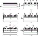
图1为根据本公开实施例GaN基单片功率变换器的结构示意图。FIG. 1 is a schematic structural diagram of a GaN-based monolithic power converter according to an embodiment of the present disclosure.
图2为根据本公开实施例GaN基单片功率变换器的制作方法流程图。2 is a flowchart of a method for fabricating a GaN-based monolithic power converter according to an embodiment of the present disclosure.
图3为根据本公开实施例GaN基单片功率变换器的制作方法中各步骤对应的结构示意图。3 is a schematic structural diagram corresponding to each step in a method for fabricating a GaN-based monolithic power converter according to an embodiment of the present disclosure.
【符号说明】【Symbol Description】
10-异质结外延衬底;10-heterojunction epitaxial substrate;
101-外延基片; 102-GaN缓冲层;101-epitaxial substrate; 102-GaN buffer layer;
103-薄势垒层; 111-二维电子气;103-thin barrier layer; 111-two-dimensional electron gas;
20-钝化层;20-passivation layer;
201-源极开口区; 202-漏极开口区;201-source opening region; 202-drain opening region;
203-栅极开口区; 204-阳极开口区;203-gate opening area; 204-anode opening area;
205-阴极开口区;205 - cathode opening area;
301-源极; 302-漏极;301-source; 302-drain;
304-阳极; 305-阴极;304-Anode; 305-Cathode;
401-第一注入隔离区; 402-第二注入隔离区;401-first implant isolation region; 402-second implant isolation region;
403-第三注入隔离区;403 - the third injection isolation region;
501-第一栅介质层; 502-第二栅介质层;501-first gate dielectric layer; 502-second gate dielectric layer;
601-第一栅极; 602-第二栅极。601 - the first gate; 602 - the second gate.
具体实施方式Detailed ways
本公开提供了一种GaN基单片功率变换器及其制作方法,通过采用超薄势垒Al(In,Ga)N/GaN异质结外延衬底,在其上沉积多晶SiN,SiO2,SiON钝化层,依次进行增强型MIS-HEMT和绝缘栅混合阳极二极管MG-HAD的制作与单片集成;整体上实现了GaN基功率二极管和三极管的集成制造,同时实现了全GaN功率转换电路,推动了GaN基单片功率集成电路向更高效能和小型紧凑化应用发展。The present disclosure provides a GaN-based monolithic power converter and a manufacturing method thereof. By using an ultra-thin barrier Al(In,Ga)N/GaN heterojunction epitaxial substrate, polycrystalline SiN, SiO2 is deposited thereon , SiON passivation layer, followed by the fabrication and monolithic integration of enhancement mode MIS-HEMT and insulated gate hybrid anode diode MG-HAD; as a whole, the integrated fabrication of GaN-based power diodes and triodes is realized, and full GaN power conversion is realized at the same time. The circuit has promoted the development of GaN-based monolithic power integrated circuits to higher efficiency and small and compact applications.
为使本公开的目的、技术方案和优点更加清楚明白,以下结合具体实施例,并参照附图,对本公开进一步详细说明。In order to make the objectives, technical solutions and advantages of the present disclosure clearer, the present disclosure will be further described in detail below with reference to the specific embodiments and the accompanying drawings.
在本公开的第一个示例性实施例中,提供了一种GaN基单片功率变换器。In a first exemplary embodiment of the present disclosure, a GaN-based monolithic power converter is provided.
图1为根据本公开实施例GaN基单片功率变换器的结构示意图。FIG. 1 is a schematic structural diagram of a GaN-based monolithic power converter according to an embodiment of the present disclosure.
参照图1所示,本公开的一种GaN基单片功率变换器,包括:异质结外延衬底10,包括:GaN缓冲层102和薄势垒层103形成的异质结,在异质结的界面处产生二维电子气111;钝化层20,形成于异质结外延衬底之上,在钝化层之间存在多个空心区域;二极管结构,形成于多个空心区域中的若干空心区域,包括:混合阳极,由阳极304和第二栅极602短接形成,阳极304与薄势垒层103实现欧姆接触,第二栅极602通过位于其下方的第二栅介质层502与薄势垒层103实现绝缘,该第二栅极602和阳极304形成于同一个空心区域;以及阴极305,与薄势垒层103实现欧姆接触;以及三极管结构,形成于多个空心区域中的其他空心区域,包括:源极301、漏极302和第一栅极601,该源极301、漏极302均与薄势垒层103实现欧姆接触,该第一栅极601通过位于其下方的第一栅介质层501与薄势垒层103实现绝缘。Referring to FIG. 1, a GaN-based monolithic power converter of the present disclosure includes: a heterojunction
下面以第一个实施例对该GaN基单片功率变换器的具体结构进行介绍。The specific structure of the GaN-based monolithic power converter will be introduced below with the first embodiment.
本实施例中的GaN基单片功率变换器,包括:The GaN-based monolithic power converter in this embodiment includes:
异质结外延衬底10;Heterojunction
钝化层20,形成于异质结外延衬底10之上,在钝化层20之间形成多个空心区域,该空心区域依次包括:源极开口区201、栅极开口区203、漏极开口区202、阳极开口区204以及阴极开口区205;The
源极301,至少覆盖源极开口区201及其两侧的部分钝化层20;The
漏极302,至少覆盖漏极开口区202及其两侧的部分钝化层20;the
阳极304,覆盖部分阳极开口区204及相邻的部分钝化层20;the
阴极305,至少覆盖阴极开口区205及其两侧的部分钝化层20;The
注入隔离区,设置于漏极302和阳极304之间以及源极301和阴极305的边缘,从钝化层20一直延伸至异质结外延衬底10的GaN缓冲层102内;The implantation isolation region is arranged between the
第一栅介质层501,至少覆盖栅极开口区203的两侧壁与底部及其两侧的部分钝化层20,与源极301、漏极302存在间隔;The first
第二栅介质层502,至少覆盖剩下的阳极开口区204的两侧壁与底部及两侧的部分阳极304和钝化层20,与阴极305存在间隔;The second
第一栅极601,形成于第一栅介质层501之上;以及a
第二栅极602,填充第二栅介质层502的内侧并跨过阳极304的欧姆和第二栅介质层502短接;The
实现增强型金属绝缘层半导体高电子迁移率晶体管(MIS-HEMT)和绝缘栅混合阳极二极管(MG-HAD)的集成。The integration of enhancement-mode metal-insulator-semiconductor high electron mobility transistor (MIS-HEMT) and insulated-gate hybrid anode diode (MG-HAD) is realized.
本实施例中,异质结外延衬底10为外延结构,自下而上依次为:外延基片101,GaN缓冲层102,以及薄势垒层103;在GaN缓冲层102与势垒层接触的异质结界面处产生二维电子气111,如图1所示。In this embodiment, the
本实施例中,外延基片101可选但不限于如下材料中的一种或几种:Si,SiC,蓝宝石或者GaN晶片等。In this embodiment, the
本实施例中,薄势垒层103可选但不限于如下材料中的一种或几种:AlGaN,AlInN三元合金或AlInGaN四元合金,其厚度介于0~6nm之间,本实施例中以Al(In,Ga)N为例进行说明。In this embodiment, the
本实施例中,采用钝化层20作为栅极以外的二维电子气的保护层,避免了在现有技术中制备MG-HAD二极管区域和MIS-HEMT栅极时对势垒层的刻蚀,有助于提高器件的成品率;同时该钝化层还作为硬质掩膜板进行源极开口区201、漏极开口区202、栅极开口区203、阳极开口区204以及阴极开口区205等空心区域的制作。In this embodiment, the
本实施例中,该钝化层20的材料可选但不限于以下材料中的一种:SiN,SiO2或SiON,其厚度介于5nm~120nm之间。In this embodiment, the material of the
本实施例中,钝化层可以采用如下方法中的一种进行制备:MOCVD(metal-organicchemical vapor deposition),LPCVD(low pressure chemical vapor deposition)或PECVD(plasma-enhanced chemical vapor deposition)等。In this embodiment, the passivation layer may be prepared by one of the following methods: MOCVD (metal-organic chemical vapor deposition), LPCVD (low pressure chemical vapor deposition), or PECVD (plasma-enhanced chemical vapor deposition) and the like.
本实施例中,通过以钝化层20作为硬质掩膜板进行源极开口区201、漏极开口区202、栅极开口区203、阳极开口区204以及阴极开口区205等空心区域的制作,然后在上述空心区域制作源极301、漏极302、阳极304、阴极305,实现欧姆接触。In this embodiment, hollow regions such as the
参照图1所示,本实施例中,将注入隔离区按照所在位置的不同分别标注为第一注入隔离区401、第二注入隔离区402以及第三注入隔离区403,其中,第一注入隔离区401位于源极301的边缘,从钝化层20一直延伸至异质结外延衬底10的GaN缓冲层102内;第二注入隔离区402位于阴极305的边缘,从钝化层20一直延伸至异质结外延衬底10的GaN缓冲层102内;第三注入隔离区403位于漏极302和阳极304之间,从钝化层20一直延伸至异质结外延衬底10的GaN缓冲层102内;这些注入隔离区实现了有源区的隔离,有助于提高击穿电压,同时设置于器件边缘,有助于减少场区漏电,提高器件的温度稳定性。Referring to FIG. 1 , in this embodiment, the injection isolation regions are respectively marked as a first
本实施例中,第一栅介质层501和第二栅介质层502的材料可选用但不限于如下材料中的一种或几种:Al2O3,SiN,SiON或SiO2等。In this embodiment, the materials of the first
如图1所示,在包括阳极304的右侧的二极管器件中,采用超薄势垒Al(In,Ga)N/GaN异质结结构形成阳极区域的增强型MIS栅,并且和欧姆接触进行叠加形成混合阳极,替代了常规的肖特基结,可获得比常规GaN基功率二极管更低的开启电压和更高的击穿电压。As shown in FIG. 1, in the diode device on the right side including the
在本公开的第二个示例性实施例中,提供了一种GaN基单片功率变换器的制作方法。In a second exemplary embodiment of the present disclosure, a method of fabricating a GaN-based monolithic power converter is provided.
图2为根据本公开实施例GaN基单片功率变换器的制作方法流程图。图3为根据本公开实施例GaN基单片功率变换器的制作方法中各步骤对应的结构示意图。2 is a flowchart of a method for fabricating a GaN-based monolithic power converter according to an embodiment of the present disclosure. 3 is a schematic structural diagram corresponding to each step in a method for fabricating a GaN-based monolithic power converter according to an embodiment of the present disclosure.
结合图2和图3所示,本公开的GaN基单片功率变换器的制作方法,包括:With reference to FIG. 2 and FIG. 3 , the manufacturing method of the GaN-based monolithic power converter of the present disclosure includes:
步骤S202:在异质结外延衬底上制备钝化层;Step S202: preparing a passivation layer on the heterojunction epitaxial substrate;
本实施例中,异质结外延衬底10为外延结构,自下而上依次为:外延基片101,GaN缓冲层102,以及薄势垒层103;在GaN缓冲层102与势垒层接触的异质结界面处产生二维电子气111。In this embodiment, the
参照图3中(a)所示,在异质结外延衬底10的外延结构上沉积一层钝化层20。Referring to FIG. 3( a ), a
本实施例中,外延基片101可选但不限于如下材料中的一种或几种:Si,SiC,蓝宝石或者GaN晶片等;薄势垒层103可选但不限于如下材料中的一种或几种:AlGaN,AlInN三元合金或AlInGaN四元合金,其厚度介于0~6nm之间,本实施例中以超薄势垒Al(In,Ga)N/GaN异质结外延衬底为例进行说明。In this embodiment, the
本实施例中,钝化层20可以采用如下方法中的一种进行制备:MOCVD(metal-organic chemical vapor deposition),LPCVD(low pressure chemical vapordeposition)或PECVD(plasma-enhanced chemical vapor deposition)等。In this embodiment, the
步骤S204:刻蚀钝化层,制备得到源极开口区、栅极开口区、漏极开口区、阳极开口区以及阴极开口区;Step S204: etching the passivation layer to prepare a source opening area, a gate opening area, a drain opening area, an anode opening area and a cathode opening area;
在如图3中(a)所示的钝化层20中刻蚀出多个空心区域,该空心区域从左至右依次包括:源极开口区201、栅极开口区203、漏极开口区202、阳极开口区204以及阴极开口区205,对应的开口区下方的二维电子气111也消失,如图3中(b)所示。A plurality of hollow regions are etched in the
本实施例中,MIS-HEMT的栅极开口区可以与源极开口区、漏极开口区同时进行打开,也可以按照先后顺序进行打开,其中,可以是源极开口区和漏极开口区先打开,也可以是栅极开口区先打开。In this embodiment, the gate opening area of the MIS-HEMT can be opened at the same time as the source opening area and the drain opening area, or can be opened sequentially, wherein the source opening area and the drain opening area can be opened first. Open, or the gate opening area can be opened first.
这里的刻蚀方法可以采用现有技术中的刻蚀手段,优选的,采用F基等离子体刻蚀,能在Al(In,Ga)N等薄势垒层的表面实现刻蚀自截止。The etching method here can use the etching means in the prior art, preferably, F-based plasma etching is used, which can realize self-cutting etching on the surface of thin barrier layers such as Al(In, Ga)N.
步骤S206:在源极开口区、漏极开口区、阴极开口区和部分阳极开口区对应沉积源极、漏极、阴极和阳极,制作欧姆接触;Step S206 : correspondingly depositing a source electrode, a drain electrode, a cathode electrode and an anode electrode in the source opening region, the drain opening region, the cathode opening region and part of the anode opening region to form ohmic contacts;
参照图3中(c)所示,在源极开口区201、漏极开口区202、阴极开口区205和部分阳极开口区204对应沉积源极301、漏极302、阴极305和阳极304,制作了欧姆接触,此时,对应填充有电极区域的二维电子气111得以恢复。Referring to FIG. 3 (c),
步骤S208:在漏极和阳极之间以及源极和阴极的边缘进行离子注入隔离;Step S208: performing ion implantation isolation between the drain electrode and the anode electrode and between the source electrode and the cathode electrode;
参照图3中(d)所示,从钝化层20一直延伸至异质结外延衬底10的GaN缓冲层102内进行离子注入;注入隔离的区域为:源极301的边缘、阴极305的边缘以及漏极302和阳极304之间,参照图3中(d)的第一注入隔离区401、第二注入隔离区402以及第三注入隔离区403所示。这些注入隔离区实现了有源区的隔离,有助于提高击穿电压,同时设置于器件边缘,有助于减少场区漏电,提高器件的温度稳定性。Referring to FIG. 3 (d), ion implantation is performed from the
步骤S210:在栅极开口区制作第一栅介质层和第一栅极,在剩下的阳极开口区制作第二栅介质层和第二栅极;完成增强型金属绝缘层半导体高电子迁移率晶体管(MIS-HEMT)和绝缘栅混合阳极二极管(MG-HAD)的集成;Step S210 : fabricating a first gate dielectric layer and a first gate electrode in the gate opening area, and fabricating a second gate dielectric layer and a second gate electrode in the remaining anode opening area; completing the enhanced metal insulating layer semiconductor high electron mobility Integration of transistors (MIS-HEMT) and insulated gate hybrid anode diodes (MG-HAD);
参照图3中(e)所示,在栅极开口区203制作第一栅介质层501,使该第一栅介质层501至少覆盖栅极开口区203的两侧壁与底部及其两侧的部分钝化层20,与源极301、漏极302存在间隔;在剩下的阳极开口区制作第二栅介质层502,使该第二栅介质层502至少覆盖剩下的阳极开口区204的两侧壁与底部及两侧的部分阳极304和钝化层20,与阴极305存在间隔;然后在第一栅介质层501上方沉积第一栅极601,在第二栅介质层502之上沉积第二栅极602,使该第二栅极602填充第二栅介质层502的内侧并将第二栅极602跨过第二栅介质层502与阳极304短接形成混合阳极,如图3中(f)所示。Referring to FIG. 3(e), a first
综上所述,本公开提供了一种GaN基单片功率变换器及其制作方法,通过采用超薄势垒Al(In,Ga)N/GaN异质外延衬底,在其上沉积多晶SiN,SiO2,SiON钝化层,依次进行增强型MIS-HEMT和绝缘栅混合阳极二极管MG-HAD的制作与单片集成;其中,阳极区域的增强型栅是由超薄势垒Al(In,Ga)N/GaN异质结构形成的,而栅极以外的二维电子气通过钝化层来恢复的,避免了MIS-HEMT栅极和MG-HAD阳极区域的Al(In,Ga)N势垒层刻蚀,有效提高了器件成品率;采用欧姆接触和增强型MIS栅叠加形成的混合阳极替代常规肖特基结,可获得比常规GaN基功率二极管更低的开启电压和更高的击穿电压;整体上实现了GaN基功率二极管和三极管的集成制造,同时实现了全GaN功率转换电路,推动了GaN基单片功率集成电路向更高效能和小型紧凑化应用发展。In summary, the present disclosure provides a GaN-based monolithic power converter and a method for fabricating the same, by using an ultra-thin barrier Al(In,Ga)N/GaN heteroepitaxial substrate on which polycrystalline SiN, SiO2 , SiON passivation layers, followed by the fabrication and monolithic integration of enhanced MIS-HEMT and insulated gate hybrid anode diode MG-HAD; wherein, the enhanced gate in the anode region is made of ultra-thin barrier Al (In , Ga)N/GaN heterostructure is formed, and the two-dimensional electron gas outside the gate is recovered through the passivation layer, avoiding the Al(In,Ga)N in the MIS-HEMT gate and MG-HAD anode region The barrier layer is etched, which effectively improves the yield of the device; the hybrid anode formed by the superposition of ohmic contact and enhanced MIS gate is used to replace the conventional Schottky junction, which can obtain lower turn-on voltage and higher power than conventional GaN-based power diodes. Breakdown voltage; as a whole, the integrated manufacturing of GaN-based power diodes and triodes is realized, and the full GaN power conversion circuit is realized, which promotes the development of GaN-based monolithic power integrated circuits to higher efficiency and small and compact applications.
需要说明的是,实施例中提到的方向用语,例如“上”、“下”、“前”、“后”、“左”、“右”等,仅是参考附图的方向,并非用来限制本公开的保护范围。贯穿附图,相同的元素由相同或相近的附图标记来表示。在可能导致对本公开的理解造成混淆时,将省略常规结构或构造。并且图中各部件的形状和尺寸不反映真实大小和比例,而仅示意本公开实施例的内容。另外,在权利要求中,不应将位于括号之间的任何参考符号构造成对权利要求的限制。It should be noted that the directional terms mentioned in the embodiments, such as "up", "down", "front", "rear", "left", "right", etc., only refer to the directions of the drawings, not to limit the scope of protection of the present disclosure. Throughout the drawings, the same elements are denoted by the same or similar reference numbers. Conventional structures or constructions will be omitted when it may lead to obscuring the understanding of the present disclosure. Moreover, the shapes and sizes of the components in the figures do not reflect the actual size and proportion, but merely illustrate the contents of the embodiments of the present disclosure. Furthermore, in the claims, any reference signs placed between parentheses shall not be construed as limiting the claim.
再者,单词“包含”或“包括”不排除存在未列在权利要求中的元件或步骤。位于元件之前的单词“一”或“一个”不排除存在多个这样的元件。Furthermore, the word "comprising" or "comprising" does not exclude the presence of elements or steps not listed in a claim. The word "a" or "an" preceding an element does not exclude the presence of a plurality of such elements.
说明书与权利要求中所使用的序数例如“第一”、“第二”、“第三”等的用词,以修饰相应的元件,其本身并不意味着该元件有任何的序数,也不代表某一元件与另一元件的顺序、或是制造方法上的顺序,该些序数的使用仅用来使具有某命名的一元件得以和另一具有相同命名的元件能做出清楚区分。The ordinal numbers such as "first", "second", "third", etc. used in the description and the claims are used to modify the corresponding elements, which themselves do not mean that the elements have any ordinal numbers, nor do they Representing the order of a certain element and another element, or the order in the manufacturing method, the use of these ordinal numbers is only used to clearly distinguish an element with a certain name from another element with the same name.
以上所述的具体实施例,对本公开的目的、技术方案和有益效果进行了进一步详细说明,所应理解的是,以上所述仅为本公开的具体实施例而已,并不用于限制本公开,凡在本公开的精神和原则之内,所做的任何修改、等同替换、改进等,均应包含在本公开的保护范围之内。The specific embodiments described above further describe the purpose, technical solutions and beneficial effects of the present disclosure in detail. It should be understood that the above-mentioned specific embodiments are only specific embodiments of the present disclosure, and are not intended to limit the present disclosure. Any modification, equivalent replacement, improvement, etc. made within the spirit and principle of the present disclosure should be included within the protection scope of the present disclosure.
Claims (10)
Priority Applications (1)
| Application Number | Priority Date | Filing Date | Title |
|---|---|---|---|
| CN201711081965.8ACN108022925B (en) | 2017-11-06 | 2017-11-06 | GaN-based monolithic power converter and manufacturing method thereof |
Applications Claiming Priority (1)
| Application Number | Priority Date | Filing Date | Title |
|---|---|---|---|
| CN201711081965.8ACN108022925B (en) | 2017-11-06 | 2017-11-06 | GaN-based monolithic power converter and manufacturing method thereof |
Publications (2)
| Publication Number | Publication Date |
|---|---|
| CN108022925A CN108022925A (en) | 2018-05-11 |
| CN108022925Btrue CN108022925B (en) | 2020-09-15 |
Family
ID=62079721
Family Applications (1)
| Application Number | Title | Priority Date | Filing Date |
|---|---|---|---|
| CN201711081965.8AActiveCN108022925B (en) | 2017-11-06 | 2017-11-06 | GaN-based monolithic power converter and manufacturing method thereof |
Country Status (1)
| Country | Link |
|---|---|
| CN (1) | CN108022925B (en) |
Families Citing this family (2)
| Publication number | Priority date | Publication date | Assignee | Title |
|---|---|---|---|---|
| CN113451402B (en)* | 2020-03-24 | 2025-04-01 | 顶诺微电子(北京)有限公司 | A power transistor |
| CN115513056B (en)* | 2022-09-16 | 2025-03-18 | 深圳天狼芯半导体有限公司 | Method for preparing HEMT semiconductor device |
Family Cites Families (5)
| Publication number | Priority date | Publication date | Assignee | Title |
|---|---|---|---|---|
| US8076699B2 (en)* | 2008-04-02 | 2011-12-13 | The Hong Kong Univ. Of Science And Technology | Integrated HEMT and lateral field-effect rectifier combinations, methods, and systems |
| KR101108746B1 (en)* | 2010-07-07 | 2012-02-24 | 삼성전기주식회사 | Nitride based semiconductor device and method for manufacturing the same |
| EP2793255B8 (en)* | 2013-04-16 | 2018-01-17 | IMEC vzw | Manufacturing method of a semiconductor device comprising a schottky diode and a high electron mobility transistor |
| US9978844B2 (en)* | 2013-08-01 | 2018-05-22 | Taiwan Semiconductor Manufacturing Co., Ltd. | HEMT-compatible lateral rectifier structure |
| CN105355657A (en)* | 2015-11-27 | 2016-02-24 | 西安电子科技大学 | Insulated gate AlGaN/GaN high electron mobility transistor with multi-channel fin structure |
- 2017
- 2017-11-06CNCN201711081965.8Apatent/CN108022925B/enactiveActive
Non-Patent Citations (1)
| Title |
|---|
| 绝缘栅GaN基平面功率开关器件技术;黄森,刘新宇等;《电力电子技术》;20170831;第51卷(第8期);65-70* |
Also Published As
| Publication number | Publication date |
|---|---|
| CN108022925A (en) | 2018-05-11 |
Similar Documents
| Publication | Publication Date | Title |
|---|---|---|
| JP6999197B2 (en) | Group III nitride enhancement type HEMT based on the composite barrier layer structure and its manufacturing method | |
| CN107887383B (en) | GaN-based monolithic power inverter and manufacturing method thereof | |
| JP6280796B2 (en) | Manufacturing method of semiconductor device having Schottky diode and high electron mobility transistor | |
| CN108604596A (en) | Field plate structure for semiconductor device | |
| CN109004033A (en) | Nitrogen polar III-nitride epitaxial structure and active device thereof and integrated polarity inversion manufacturing method thereof | |
| TW201419546A (en) | Transistor and its forming method and semiconductor component | |
| CN108649071A (en) | Semiconductor devices and its manufacturing method | |
| CN110429127B (en) | Gallium nitride transistor structure and preparation method thereof | |
| WO2020181548A1 (en) | Gan-based super-junction vertical power transistor and manufacturing method therefor | |
| CN111048411A (en) | Manufacturing method of semiconductor device | |
| JP5645766B2 (en) | Method for manufacturing GaN-based thin film transistors | |
| CN102376760B (en) | Enhanced high electron mobility transistor and manufacturing method thereof | |
| US20110057233A1 (en) | Semiconductor component and method for manufacturing of the same | |
| CN106257686A (en) | Semiconductor device and manufacture method thereof | |
| WO2020206960A1 (en) | High electron mobility transistor (hemt) and fabrication method therefor | |
| CN111627988A (en) | Semiconductor device and preparation method thereof | |
| CN108022925B (en) | GaN-based monolithic power converter and manufacturing method thereof | |
| CN111599857A (en) | Two-dimensional material device and GaN device hetero-integrated structure and preparation method | |
| TW202329461A (en) | High electron mobility transistor and method for fabricating the same | |
| JP2013175726A (en) | ENHANCEMENT MODE GaN HEMT DEVICE WITH GATE SPACER AND METHOD FOR FABRICATING THE SAME | |
| CN117133806B (en) | A natural superjunction GaN HEMT device and its preparation method | |
| CN106601806A (en) | Semiconductor device and manufacture method thereof | |
| CN105679679B (en) | A kind of preparation method of GaN base notched gates MISFET | |
| CN216213472U (en) | semiconductor device | |
| CN111755330A (en) | A kind of semiconductor structure and its manufacturing method |
Legal Events
| Date | Code | Title | Description |
|---|---|---|---|
| PB01 | Publication | ||
| PB01 | Publication | ||
| SE01 | Entry into force of request for substantive examination | ||
| SE01 | Entry into force of request for substantive examination | ||
| GR01 | Patent grant | ||
| GR01 | Patent grant |