CN107968067B - Method and apparatus for fabricating heterostructures with reduced strain by radial expansion - Google Patents
Method and apparatus for fabricating heterostructures with reduced strain by radial expansionDownload PDFInfo
- Publication number
- CN107968067B CN107968067BCN201810030851.9ACN201810030851ACN107968067BCN 107968067 BCN107968067 BCN 107968067BCN 201810030851 ACN201810030851 ACN 201810030851ACN 107968067 BCN107968067 BCN 107968067B
- Authority
- CN
- China
- Prior art keywords
- semiconductor structure
- substrate
- layer
- top plate
- peripheral
- Prior art date
- Legal status (The legal status is an assumption and is not a legal conclusion. Google has not performed a legal analysis and makes no representation as to the accuracy of the status listed.)
- Active
Links
- 238000000034methodMethods0.000titleabstractdescription32
- 239000004065semiconductorSubstances0.000claimsabstractdescription81
- 230000002093peripheral effectEffects0.000claimsdescription43
- 239000012530fluidSubstances0.000claimsdescription11
- 238000004891communicationMethods0.000claimsdescription8
- 230000006835compressionEffects0.000claimsdescription7
- 238000007906compressionMethods0.000claimsdescription7
- 238000010438heat treatmentMethods0.000claimsdescription5
- 239000002344surface layerSubstances0.000abstractdescription40
- 230000007547defectEffects0.000abstract1
- 239000000758substrateSubstances0.000description151
- 239000010410layerSubstances0.000description131
- 230000035882stressEffects0.000description39
- 239000000463materialSubstances0.000description21
- 150000002500ionsChemical class0.000description20
- 229910000577Silicon-germaniumInorganic materials0.000description14
- 229910052710siliconInorganic materials0.000description14
- 239000010703siliconSubstances0.000description14
- XUIMIQQOPSSXEZ-UHFFFAOYSA-NSiliconChemical compound[Si]XUIMIQQOPSSXEZ-UHFFFAOYSA-N0.000description13
- 235000012431wafersNutrition0.000description12
- 238000000576coating methodMethods0.000description11
- 239000011248coating agentSubstances0.000description10
- 238000000151depositionMethods0.000description10
- 125000004429atomChemical group0.000description9
- 229910052732germaniumInorganic materials0.000description9
- 239000010408filmSubstances0.000description8
- 238000000227grindingMethods0.000description7
- 230000004913activationEffects0.000description6
- 230000008021depositionEffects0.000description5
- 230000010339dilationEffects0.000description5
- 239000007943implantSubstances0.000description5
- 229910021421monocrystalline siliconInorganic materials0.000description5
- 208000035208Ring chromosome 20 syndromeDiseases0.000description4
- LEVVHYCKPQWKOP-UHFFFAOYSA-N[Si].[Ge]Chemical compound[Si].[Ge]LEVVHYCKPQWKOP-UHFFFAOYSA-N0.000description4
- 239000013078crystalSubstances0.000description4
- GNPVGFCGXDBREM-UHFFFAOYSA-Ngermanium atomChemical compound[Ge]GNPVGFCGXDBREM-UHFFFAOYSA-N0.000description4
- 230000002040relaxant effectEffects0.000description4
- -1silicon ionsChemical class0.000description4
- JBRZTFJDHDCESZ-UHFFFAOYSA-NAsGaChemical compound[As]#[Ga]JBRZTFJDHDCESZ-UHFFFAOYSA-N0.000description3
- 229910001218Gallium arsenideInorganic materials0.000description3
- 229910000530Gallium indium arsenideInorganic materials0.000description3
- KXNLCSXBJCPWGL-UHFFFAOYSA-N[Ga].[As].[In]Chemical compound[Ga].[As].[In]KXNLCSXBJCPWGL-UHFFFAOYSA-N0.000description3
- QVGXLLKOCUKJST-UHFFFAOYSA-Natomic oxygenChemical compound[O]QVGXLLKOCUKJST-UHFFFAOYSA-N0.000description3
- 238000005229chemical vapour depositionMethods0.000description3
- 238000007796conventional methodMethods0.000description3
- 230000006355external stressEffects0.000description3
- 238000002513implantationMethods0.000description3
- 238000007373indentationMethods0.000description3
- 239000012212insulatorSubstances0.000description3
- 239000001301oxygenSubstances0.000description3
- 229910052760oxygenInorganic materials0.000description3
- HBMJWWWQQXIZIP-UHFFFAOYSA-Nsilicon carbideChemical compound[Si+]#[C-]HBMJWWWQQXIZIP-UHFFFAOYSA-N0.000description3
- 229910010271silicon carbideInorganic materials0.000description3
- 230000003313weakening effectEffects0.000description3
- XKRFYHLGVUSROY-UHFFFAOYSA-NArgonChemical compound[Ar]XKRFYHLGVUSROY-UHFFFAOYSA-N0.000description2
- 229910002601GaNInorganic materials0.000description2
- JMASRVWKEDWRBT-UHFFFAOYSA-NGallium nitrideChemical compound[Ga]#NJMASRVWKEDWRBT-UHFFFAOYSA-N0.000description2
- 229910021417amorphous siliconInorganic materials0.000description2
- 238000001505atmospheric-pressure chemical vapour depositionMethods0.000description2
- 238000000231atomic layer depositionMethods0.000description2
- 230000015572biosynthetic processEffects0.000description2
- PMHQVHHXPFUNSP-UHFFFAOYSA-Mcopper(1+);methylsulfanylmethane;bromideChemical compoundBr[Cu].CSCPMHQVHHXPFUNSP-UHFFFAOYSA-M0.000description2
- 230000008020evaporationEffects0.000description2
- 238000001704evaporationMethods0.000description2
- 230000005669field effectEffects0.000description2
- 238000004519manufacturing processMethods0.000description2
- 238000010297mechanical methods and processMethods0.000description2
- 239000012528membraneSubstances0.000description2
- 239000000203mixtureSubstances0.000description2
- 229910052594sapphireInorganic materials0.000description2
- 239000010980sapphireSubstances0.000description2
- 239000010409thin filmSubstances0.000description2
- 238000012546transferMethods0.000description2
- 238000000038ultrahigh vacuum chemical vapour depositionMethods0.000description2
- 229910052582BNInorganic materials0.000description1
- 229910016036BaF 2Inorganic materials0.000description1
- PZNSFCLAULLKQX-UHFFFAOYSA-NBoron nitrideChemical compoundN#BPZNSFCLAULLKQX-UHFFFAOYSA-N0.000description1
- 229910004261CaF 2Inorganic materials0.000description1
- OKTJSMMVPCPJKN-UHFFFAOYSA-NCarbonChemical compound[C]OKTJSMMVPCPJKN-UHFFFAOYSA-N0.000description1
- 229910010038TiAlInorganic materials0.000description1
- 230000003213activating effectEffects0.000description1
- 229910052786argonInorganic materials0.000description1
- 230000001143conditioned effectEffects0.000description1
- 230000001276controlling effectEffects0.000description1
- 238000001816coolingMethods0.000description1
- 238000002109crystal growth methodMethods0.000description1
- 125000004122cyclic groupChemical group0.000description1
- 230000001351cycling effectEffects0.000description1
- 230000007423decreaseEffects0.000description1
- 230000003247decreasing effectEffects0.000description1
- 230000002950deficientEffects0.000description1
- 238000001514detection methodMethods0.000description1
- 238000010586diagramMethods0.000description1
- 230000000694effectsEffects0.000description1
- 238000004049embossingMethods0.000description1
- 239000002783friction materialSubstances0.000description1
- 229910002804graphiteInorganic materials0.000description1
- 239000010439graphiteSubstances0.000description1
- 229910052734heliumInorganic materials0.000description1
- 239000001307heliumSubstances0.000description1
- SWQJXJOGLNCZEY-UHFFFAOYSA-Nhelium atomChemical compound[He]SWQJXJOGLNCZEY-UHFFFAOYSA-N0.000description1
- 229910052739hydrogenInorganic materials0.000description1
- 239000001257hydrogenSubstances0.000description1
- 125000004435hydrogen atomChemical class[H]*0.000description1
- 238000002347injectionMethods0.000description1
- 239000007924injectionSubstances0.000description1
- 238000005468ion implantationMethods0.000description1
- 239000011159matrix materialSubstances0.000description1
- 238000005259measurementMethods0.000description1
- 238000001451molecular beam epitaxyMethods0.000description1
- 229910052754neonInorganic materials0.000description1
- GKAOGPIIYCISHV-UHFFFAOYSA-Nneon atomChemical compound[Ne]GKAOGPIIYCISHV-UHFFFAOYSA-N0.000description1
- 230000007935neutral effectEffects0.000description1
- 238000009828non-uniform distributionMethods0.000description1
- 238000002360preparation methodMethods0.000description1
- 238000012545processingMethods0.000description1
- 230000001105regulatory effectEffects0.000description1
- 238000005070samplingMethods0.000description1
- 238000005488sandblastingMethods0.000description1
- 239000000126substanceSubstances0.000description1
- 229910052724xenonInorganic materials0.000description1
- FHNFHKCVQCLJFQ-UHFFFAOYSA-Nxenon atomChemical compound[Xe]FHNFHKCVQCLJFQ-UHFFFAOYSA-N0.000description1
Images


Classifications
- H—ELECTRICITY
- H01—ELECTRIC ELEMENTS
- H01L—SEMICONDUCTOR DEVICES NOT COVERED BY CLASS H10
- H01L21/00—Processes or apparatus adapted for the manufacture or treatment of semiconductor or solid state devices or of parts thereof
- H01L21/02—Manufacture or treatment of semiconductor devices or of parts thereof
- H01L21/04—Manufacture or treatment of semiconductor devices or of parts thereof the devices having potential barriers, e.g. a PN junction, depletion layer or carrier concentration layer
- H01L21/18—Manufacture or treatment of semiconductor devices or of parts thereof the devices having potential barriers, e.g. a PN junction, depletion layer or carrier concentration layer the devices having semiconductor bodies comprising elements of Group IV of the Periodic Table or AIIIBV compounds with or without impurities, e.g. doping materials
- H01L21/30—Treatment of semiconductor bodies using processes or apparatus not provided for in groups H01L21/20 - H01L21/26
- H01L21/322—Treatment of semiconductor bodies using processes or apparatus not provided for in groups H01L21/20 - H01L21/26 to modify their internal properties, e.g. to produce internal imperfections
- H—ELECTRICITY
- H01—ELECTRIC ELEMENTS
- H01L—SEMICONDUCTOR DEVICES NOT COVERED BY CLASS H10
- H01L21/00—Processes or apparatus adapted for the manufacture or treatment of semiconductor or solid state devices or of parts thereof
- H01L21/67—Apparatus specially adapted for handling semiconductor or electric solid state devices during manufacture or treatment thereof; Apparatus specially adapted for handling wafers during manufacture or treatment of semiconductor or electric solid state devices or components ; Apparatus not specifically provided for elsewhere
- H01L21/683—Apparatus specially adapted for handling semiconductor or electric solid state devices during manufacture or treatment thereof; Apparatus specially adapted for handling wafers during manufacture or treatment of semiconductor or electric solid state devices or components ; Apparatus not specifically provided for elsewhere for supporting or gripping
- H01L21/687—Apparatus specially adapted for handling semiconductor or electric solid state devices during manufacture or treatment thereof; Apparatus specially adapted for handling wafers during manufacture or treatment of semiconductor or electric solid state devices or components ; Apparatus not specifically provided for elsewhere for supporting or gripping using mechanical means, e.g. chucks, clamps or pinches
- H01L21/68714—Apparatus specially adapted for handling semiconductor or electric solid state devices during manufacture or treatment thereof; Apparatus specially adapted for handling wafers during manufacture or treatment of semiconductor or electric solid state devices or components ; Apparatus not specifically provided for elsewhere for supporting or gripping using mechanical means, e.g. chucks, clamps or pinches the wafers being placed on a susceptor, stage or support
- H01L21/68735—Apparatus specially adapted for handling semiconductor or electric solid state devices during manufacture or treatment thereof; Apparatus specially adapted for handling wafers during manufacture or treatment of semiconductor or electric solid state devices or components ; Apparatus not specifically provided for elsewhere for supporting or gripping using mechanical means, e.g. chucks, clamps or pinches the wafers being placed on a susceptor, stage or support characterised by edge profile or support profile
- C—CHEMISTRY; METALLURGY
- C30—CRYSTAL GROWTH
- C30B—SINGLE-CRYSTAL GROWTH; UNIDIRECTIONAL SOLIDIFICATION OF EUTECTIC MATERIAL OR UNIDIRECTIONAL DEMIXING OF EUTECTOID MATERIAL; REFINING BY ZONE-MELTING OF MATERIAL; PRODUCTION OF A HOMOGENEOUS POLYCRYSTALLINE MATERIAL WITH DEFINED STRUCTURE; SINGLE CRYSTALS OR HOMOGENEOUS POLYCRYSTALLINE MATERIAL WITH DEFINED STRUCTURE; AFTER-TREATMENT OF SINGLE CRYSTALS OR A HOMOGENEOUS POLYCRYSTALLINE MATERIAL WITH DEFINED STRUCTURE; APPARATUS THEREFOR
- C30B25/00—Single-crystal growth by chemical reaction of reactive gases, e.g. chemical vapour-deposition growth
- C30B25/02—Epitaxial-layer growth
- C30B25/12—Substrate holders or susceptors
- H—ELECTRICITY
- H01—ELECTRIC ELEMENTS
- H01L—SEMICONDUCTOR DEVICES NOT COVERED BY CLASS H10
- H01L21/00—Processes or apparatus adapted for the manufacture or treatment of semiconductor or solid state devices or of parts thereof
- H01L21/02—Manufacture or treatment of semiconductor devices or of parts thereof
- H01L21/04—Manufacture or treatment of semiconductor devices or of parts thereof the devices having potential barriers, e.g. a PN junction, depletion layer or carrier concentration layer
- H01L21/18—Manufacture or treatment of semiconductor devices or of parts thereof the devices having potential barriers, e.g. a PN junction, depletion layer or carrier concentration layer the devices having semiconductor bodies comprising elements of Group IV of the Periodic Table or AIIIBV compounds with or without impurities, e.g. doping materials
- H01L21/30—Treatment of semiconductor bodies using processes or apparatus not provided for in groups H01L21/20 - H01L21/26
- H01L21/302—Treatment of semiconductor bodies using processes or apparatus not provided for in groups H01L21/20 - H01L21/26 to change their surface-physical characteristics or shape, e.g. etching, polishing, cutting
- H—ELECTRICITY
- H01—ELECTRIC ELEMENTS
- H01L—SEMICONDUCTOR DEVICES NOT COVERED BY CLASS H10
- H01L21/00—Processes or apparatus adapted for the manufacture or treatment of semiconductor or solid state devices or of parts thereof
- H01L21/67—Apparatus specially adapted for handling semiconductor or electric solid state devices during manufacture or treatment thereof; Apparatus specially adapted for handling wafers during manufacture or treatment of semiconductor or electric solid state devices or components ; Apparatus not specifically provided for elsewhere
- H01L21/67005—Apparatus not specifically provided for elsewhere
- H01L21/67011—Apparatus for manufacture or treatment
- H01L21/67092—Apparatus for mechanical treatment
- H—ELECTRICITY
- H01—ELECTRIC ELEMENTS
- H01L—SEMICONDUCTOR DEVICES NOT COVERED BY CLASS H10
- H01L21/00—Processes or apparatus adapted for the manufacture or treatment of semiconductor or solid state devices or of parts thereof
- H01L21/67—Apparatus specially adapted for handling semiconductor or electric solid state devices during manufacture or treatment thereof; Apparatus specially adapted for handling wafers during manufacture or treatment of semiconductor or electric solid state devices or components ; Apparatus not specifically provided for elsewhere
- H01L21/683—Apparatus specially adapted for handling semiconductor or electric solid state devices during manufacture or treatment thereof; Apparatus specially adapted for handling wafers during manufacture or treatment of semiconductor or electric solid state devices or components ; Apparatus not specifically provided for elsewhere for supporting or gripping
- H01L21/6838—Apparatus specially adapted for handling semiconductor or electric solid state devices during manufacture or treatment thereof; Apparatus specially adapted for handling wafers during manufacture or treatment of semiconductor or electric solid state devices or components ; Apparatus not specifically provided for elsewhere for supporting or gripping with gripping and holding devices using a vacuum; Bernoulli devices
- H—ELECTRICITY
- H01—ELECTRIC ELEMENTS
- H01L—SEMICONDUCTOR DEVICES NOT COVERED BY CLASS H10
- H01L21/00—Processes or apparatus adapted for the manufacture or treatment of semiconductor or solid state devices or of parts thereof
- H01L21/67—Apparatus specially adapted for handling semiconductor or electric solid state devices during manufacture or treatment thereof; Apparatus specially adapted for handling wafers during manufacture or treatment of semiconductor or electric solid state devices or components ; Apparatus not specifically provided for elsewhere
- H01L21/683—Apparatus specially adapted for handling semiconductor or electric solid state devices during manufacture or treatment thereof; Apparatus specially adapted for handling wafers during manufacture or treatment of semiconductor or electric solid state devices or components ; Apparatus not specifically provided for elsewhere for supporting or gripping
- H01L21/687—Apparatus specially adapted for handling semiconductor or electric solid state devices during manufacture or treatment thereof; Apparatus specially adapted for handling wafers during manufacture or treatment of semiconductor or electric solid state devices or components ; Apparatus not specifically provided for elsewhere for supporting or gripping using mechanical means, e.g. chucks, clamps or pinches
- H01L21/68714—Apparatus specially adapted for handling semiconductor or electric solid state devices during manufacture or treatment thereof; Apparatus specially adapted for handling wafers during manufacture or treatment of semiconductor or electric solid state devices or components ; Apparatus not specifically provided for elsewhere for supporting or gripping using mechanical means, e.g. chucks, clamps or pinches the wafers being placed on a susceptor, stage or support
- H01L21/6875—Apparatus specially adapted for handling semiconductor or electric solid state devices during manufacture or treatment thereof; Apparatus specially adapted for handling wafers during manufacture or treatment of semiconductor or electric solid state devices or components ; Apparatus not specifically provided for elsewhere for supporting or gripping using mechanical means, e.g. chucks, clamps or pinches the wafers being placed on a susceptor, stage or support characterised by a plurality of individual support members, e.g. support posts or protrusions
Landscapes
- Engineering & Computer Science (AREA)
- Physics & Mathematics (AREA)
- Condensed Matter Physics & Semiconductors (AREA)
- General Physics & Mathematics (AREA)
- Manufacturing & Machinery (AREA)
- Computer Hardware Design (AREA)
- Microelectronics & Electronic Packaging (AREA)
- Power Engineering (AREA)
- Chemical & Material Sciences (AREA)
- General Chemical & Material Sciences (AREA)
- Chemical Kinetics & Catalysis (AREA)
- Crystallography & Structural Chemistry (AREA)
- Materials Engineering (AREA)
- Metallurgy (AREA)
- Organic Chemistry (AREA)
- Recrystallisation Techniques (AREA)
- Container, Conveyance, Adherence, Positioning, Of Wafer (AREA)
- Crystals, And After-Treatments Of Crystals (AREA)
- Chemical Vapour Deposition (AREA)
- Semiconductor Lasers (AREA)
Abstract
Description
Translated fromChinese本申请是申请日为2013年12月30日、申请号为201380073264.3、名称为"用于制备具有通过径向扩张降低的应变的异质结构的方法和装置"的专利申请的分案申请。This application is a divisional application of a patent application with a filing date of December 30, 2013, an application number of 201380073264.3, and a title of "Method and Apparatus for Fabricating a Heterostructure with Reduced Strain Through Radial Expansion".
相关申请的交叉引用Cross References to Related Applications
本申请要求2012年12月31日提交的美国临时申请号61/747,613;2013年3月15日提交的美国临时申请号61/793,999;2013年3月15日提交的美国临时申请号61/790,445以及2013年3月15日提交的美国临时申请号61/788,744的优选权,其中每一个通过引用并入到这里。This application claims U.S. Provisional Application No. 61/747,613, filed December 31, 2012; U.S. Provisional Application No. 61/793,999, filed March 15, 2013; U.S. Provisional Application No. 61/790,445, filed March 15, 2013 and the priority of U.S. Provisional Application No. 61/788,744, filed March 15, 2013, each of which is hereby incorporated by reference.
技术领域technical field
本公开内容通常涉及具有降低的应变的半导体异质结构的制备,并且特别地,涉及具有半导体衬底的异质结构,其顺应具有与衬底不同的晶格常数的表面层,从而形成相对低缺陷的异质结构。The present disclosure relates generally to the fabrication of semiconductor heterostructures with reduced strain, and in particular, to heterostructures having a semiconductor substrate conforming to a surface layer having a different lattice constant than the substrate, thereby forming a relatively low Defective heterostructure.
背景技术Background technique
包括具有器件质量表面的器件层和具有与器件层的材料不同的晶格结构的衬底的多层结构对许多不同目的有用。这些多层结构典型地包含具有不同的晶格常数的材料的多层。在层之间的晶格失配导致层要被应变。在器件层中失配位错自发地形成以弛豫(relax)在层之间的应变。这样的位错降低多层半导体结构的质量和效用。Multilayer structures comprising a device layer having a device-quality surface and a substrate having a lattice structure different from the material of the device layer are useful for many different purposes. These multilayer structures typically contain multiple layers of materials with different lattice constants. Lattice mismatch between layers causes the layers to be strained. Misfit dislocations form spontaneously in the device layers to relax the strain between the layers. Such dislocations degrade the quality and utility of the multilayer semiconductor structure.
出现对于用于弛豫在晶格失配的半导体层之间的应变的方法和对于导致基本上没有位错的衬底和器件层的方法的继续需要。There is a continuing need for methods for relaxing strain between lattice-mismatched semiconductor layers and for methods that result in substantially dislocation-free substrate and device layers.
发明内容Contents of the invention
本公开内容的一方面旨在一种用于在异质结构中弛豫应变的方法,所述异质结构包括衬底、在所述衬底上设置的表面层以及在所述衬底和所述表面层之间的界面。所述衬底包含中心轴、通常垂直于所述中心轴的背表面以及穿过所述中心轴跨所述衬底延伸的直径。在所述衬底中形成位错源层。将所述衬底径向扩张以产生位错并且从所述位错源层将所述位错朝向所述表面层滑动。An aspect of the present disclosure is directed to a method for relaxing strain in a heterostructure comprising a substrate, a surface layer disposed on the substrate, and a layer between the substrate and the interface between the surface layers. The substrate includes a central axis, a back surface generally perpendicular to the central axis, and a diameter extending across the substrate through the central axis. A dislocation source layer is formed in the substrate. The substrate is radially expanded to generate dislocations and slide the dislocations from the dislocation source layer towards the surface layer.
本公开内容的另一方面旨在一种用于制备弛豫的异质结构的方法。在所述半导体衬底的前表面上沉积表面层,从而在所述表面层与所述衬底之间产生应变。在所述衬底中形成位错源层。通过径向扩张所述衬底弛豫在所述表面层与所述衬底中的所述应变,以产生位错并且从所述位错源层将所述位错朝向所述表面层滑动。Another aspect of the disclosure is directed to a method for preparing a relaxed heterostructure. A surface layer is deposited on the front surface of the semiconductor substrate, thereby creating a strain between the surface layer and the substrate. A dislocation source layer is formed in the substrate. The strain in the surface layer and the substrate is relaxed by radially expanding the substrate to generate dislocations and slide the dislocations from the dislocation source layer towards the surface layer.
本公开内容的又一方面旨在一种用于径向扩张具有前表面、背表面以及周向边缘的半导体结构的装置。所述装置包括结构夹持物,所述结构夹持物包括用于邻近所述结构的周向边缘接触所述结构的顶板和背板。所述顶板适合于接触所述结构的所述前表面,并且所述背板适合于接触所述结构的所述背表面。所述顶板和背板进一步适合于在所述顶板、背板以及所述结构的周向边缘之间形成外围腔。Yet another aspect of the present disclosure is directed to an apparatus for radially expanding a semiconductor structure having a front surface, a back surface and a circumferential edge. The device includes a structure holder including a top plate and a back plate for contacting the structure adjacent a circumferential edge of the structure. The top plate is adapted to contact the front surface of the structure and the back plate is adapted to contact the back surface of the structure. The top and back plates are further adapted to form a peripheral cavity between the top and back plates and the circumferential edges of the structure.
本公开内容的附加方面旨在一种用于径向扩张具有前表面、背表面、周向边缘以及中心轴的半导体结构的装置。所述装置包括向内指向中心轴的三角形-形状段。所述段被配置为用于从所述中心轴向外移动以使得所述结构扩张。在每个段中形成流体通道用于在所述段与结构之间形成真空。An additional aspect of the present disclosure is directed to an apparatus for radially expanding a semiconductor structure having a front surface, a back surface, a circumferential edge, and a central axis. The device comprises triangular-shaped segments pointing inwards towards a central axis. The segments are configured for movement outwardly from the central axis to expand the structure. Fluid channels are formed in each segment for creating a vacuum between the segment and the structure.
附图说明Description of drawings
图1为硅异质结构的截面示意图;1 is a schematic cross-sectional view of a silicon heterostructure;
图2为示出用于制备异质结构的方法的流程图;Figure 2 is a flow diagram illustrating a method for preparing a heterostructure;
图3-4为半导体结构和用于扩张半导体结构的结构夹持物的截面图;3-4 are cross-sectional views of a semiconductor structure and a structure holder for expanding the semiconductor structure;
图5为半导体结构和用于扩张半导体结构的结构夹持物的另一实施例的截面图;5 is a cross-sectional view of another embodiment of a semiconductor structure and a structure holder for expanding the semiconductor structure;
图6-7为具有涂层在其上的半导体结构和图3的结构夹持物的截面图;6-7 are cross-sectional views of a semiconductor structure having a coating thereon and the structure holder of FIG. 3;
图8为半导体结构和用于扩张在其中设置有图3的结构夹持物的结构的装置的截面示意图;8 is a schematic cross-sectional view of a semiconductor structure and an apparatus for expanding the structure having the structure holder of FIG. 3 disposed therein;
图9为半导体结构和用于扩张半导体结构的结构夹持物的另一实施例的截面图;9 is a cross-sectional view of another embodiment of a semiconductor structure and a structure holder for expanding the semiconductor structure;
图10为半导体结构和具有用于扩张半导体结构的压缩板的结构夹持物的截面图;10 is a cross-sectional view of a semiconductor structure and a structure holder with compression plates for expanding the semiconductor structure;
图11为半导体结构和用于扩张半导体结构的结构夹持物的另一实施例的截面图;11 is a cross-sectional view of another embodiment of a semiconductor structure and a structure holder for expanding the semiconductor structure;
图12为半导体结构和用于扩张半导体结构的结构夹持物的另一实施例的截面图;12 is a cross-sectional view of another embodiment of a semiconductor structure and a structure holder for expanding the semiconductor structure;
图13为半导体结构和具有用于扩张半导体结构的压缩板的结构夹持物的截面图;13 is a cross-sectional view of a semiconductor structure and a structure holder with compression plates for expanding the semiconductor structure;
图14为多个半导体结构和用于扩张半导体结构的结构夹持物的截面图;14 is a cross-sectional view of a plurality of semiconductor structures and a structure holder for expanding the semiconductor structures;
图15为多个半导体结构和用于扩张半导体结构的结构夹持物的另一实施例的截面图;15 is a cross-sectional view of another embodiment of a plurality of semiconductor structures and a structure holder for expanding the semiconductor structures;
图16为用于扩张半导体结构的结构夹持物的另一实施例的顶视图;16 is a top view of another embodiment of a structure holder for expanding a semiconductor structure;
图17为半导体结构和用于扩张半导体结构的结构夹持物的另一实施例的截面图;17 is a cross-sectional view of another embodiment of a semiconductor structure and a structure holder for expanding the semiconductor structure;
图18为具有槽的半导体结构和用于扩张半导体结构的结构夹持物的另一实施例的截面图;18 is a cross-sectional view of another embodiment of a semiconductor structure having a trench and a structure holder for expanding the semiconductor structure;
图19为半导体结构和具有顶板的图18的结构夹持物的截面图;19 is a cross-sectional view of a semiconductor structure and the structure holder of FIG. 18 with a top plate;
图20为具有两个槽的半导体结构和用于扩张半导体结构的结构夹持物的另一实施例的截面图;20 is a cross-sectional view of another embodiment of a semiconductor structure having two trenches and a structure holder for expanding the semiconductor structure;
图21为半导体结构和具有凸缘的结构夹持物的另一实施例的截面图;21 is a cross-sectional view of another embodiment of a semiconductor structure and a structure holder with flanges;
在整个附图中相应的参考字符表示相应的部分。Corresponding reference characters indicate corresponding parts throughout the drawings.
具体实施方式Detailed ways
依照本公开内容的一个或多个方面,具有在衬底与具有与衬底不同的晶格常数的表面层之间的降低的应变的异质结构被诸如通过图2的方法制备。此处表面层也被称为“外延层”、“异质外延层”、“沉积膜”、“膜”、“异质层”或“沉积层”。可以形成具有基本上弛豫的表面层和降低的失配位错的浓度的异质结构,该失配位错也被称为穿透(threading)位错。In accordance with one or more aspects of the present disclosure, a heterostructure with reduced strain between a substrate and a surface layer having a different lattice constant than the substrate is prepared such as by the method of FIG. 2 . The surface layer is also referred to herein as "epitaxial layer", "heteroepitaxial layer", "deposited film", "membrane", "heterogeneous layer" or "deposited layer". A heterostructure can be formed with a substantially relaxed surface layer and a reduced concentration of misfit dislocations, also known as threading dislocations.
通常,本公开内容的方法包括在半导体衬底中形成位错源层,在位错源层的形成之前或之后在衬底上沉积异质层,并且径向扩张异质结构以产生(即,“激活”)位错,以及从位错源层滑动位错朝向表面层。通过施加应力(例如,张力)到衬底同时发生源层的激活和从源层朝向具有沉积层的界面的位错的滑动。在一个或多个步骤中并且以各种组合施加应力,以激活并滑动位错,从而塑性拉伸异质结构。In general, methods of the present disclosure include forming a dislocation source layer in a semiconductor substrate, depositing a heterogeneous layer on the substrate either before or after formation of the dislocation source layer, and radially expanding the heterostructure to produce (i.e., "Activation") dislocations, and sliding dislocations from the dislocation source layer towards the surface layer. Activation of the source layer and sliding of dislocations from the source layer towards the interface with the deposited layer occur simultaneously by applying stress (eg, tension) to the substrate. Stress is applied in one or more steps and in various combinations to activate and slide dislocations to plastically stretch the heterostructure.
异质层具有晶格常数aSl,其不同于衬底的天然晶格常数aS,以在衬底的表面上形成膜。通常,异质层的晶格常数aSl大于衬底的天然晶格常数aS,以便通过控制通过扩张在衬底中的位错环的产生与滑动,塑性变形衬底并且更适合地对准膜的晶格,从而允许膜被完全地弛豫膜并且在衬底上具有降低的密度的穿透位错。The heterogeneous layer has a lattice constant aSl that is different from the natural lattice constant aS of the substrate to form a film on the surface of the substrate. Usually, the lattice constantaSl of the heterogeneous layer is larger than the natural lattice constantaS of the substrate, so that by controlling the generation and sliding of dislocation loops in the substrate by expanding, the substrate is plastically deformed and more properly aligned The crystal lattice of the film, allowing the film to be completely relaxed and have a reduced density of threading dislocations on the substrate.
本公开内容的方法具有超过用于弛豫异质层的常规的方法的若干优势。常规方法在膜与衬底之间的应力中产生大的不对称,其导致在应力为最大的地方(即,膜)的位错生成。通过将位错环限制于膜,位错留下段作为降低的穿透位错。已经采用许多的努力试图最小化这样的穿透位错的密度。The method of the present disclosure has several advantages over conventional methods for relaxing heterogeneous layers. Conventional methods create large asymmetries in the stress between the film and substrate, which lead to dislocation generation where the stress is greatest (ie, the film). By confining the dislocation loops to the membrane, the dislocations leave segments as reduced threading dislocations. Numerous efforts have been made to try to minimize the density of such threading dislocations.
对比而言,本公开内容的方法用在衬底中发生的位错生成导致应力的不对称(例如,通过弱化衬底且在弱化衬底时在其中使用相对薄的膜以避免错生成)。这允许限制位错到衬底,同时在衬底与膜之间的界面处形成失配位错层。当通过各种可控的方式引入位错而弱化衬底时,施加外部应力到系统以激活位错。这不同于常规方法,其由于相对大的本征、内部应力导致自弛豫(即,弛豫而没有外部应力的施加)。本公开内容的方法涉及弛豫而不是通过自弛豫,通过用相对薄的膜在适当的温度弱化和应用的外部应力从而没有发生自弛豫。In contrast, the methods of the present disclosure result in an asymmetry of stress with dislocation generation occurring in the substrate (eg, by weakening the substrate and using a relatively thin film therein to avoid dislocation generation when weakening the substrate). This allows confinement of dislocations to the substrate while forming a layer of misfit dislocations at the interface between the substrate and the film. While the substrate is weakened by introducing dislocations in various controllable ways, external stress is applied to the system to activate the dislocations. This differs from conventional methods, which result in self-relaxation (ie, relaxation without application of external stress) due to the relatively large intrinsic, internal stress. The method of the present disclosure involves relaxation rather than through self-relaxation by weakening with a relatively thin film at an appropriate temperature and applied external stress so that self-relaxation does not occur.
I.半导体衬底I. Semiconductor substrate
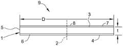
参照图1,半导体衬底1可能为适合于用作用于支撑表面层的衬底的任何单晶半导体材料,该表面层诸如,通过化学气相沉积的外延层的沉积。通常,半导体衬底由选自下列的材料组成:硅、碳化硅、蓝宝石、锗、锗硅、氮化镓、氮化铝、砷化镓、铟镓砷或及其任何组合。典型地,半导体衬底由硅组成。Referring to Figure 1, the
半导体衬底1为如在下文中更详细的描述的适合于使用作为用于沉积表面层的衬底和适合于施加应力到衬底材料的任何形状。典型地,半导体衬底具有中心轴2;具有沉积层7和背表面4的界面3,衬底-表面层界面3和背表面4通常垂直于中心轴2;厚度t,对应于从界面到衬底的背表面的距离;周向边缘5;以及直径D,通过中心轴跨衬底延伸。应当指出,用于阐述目的,将背表面4描述为在其处或其附近将形成位错源层的相对表面,并且照此在此处被称为“相对表面”和/或“受损的表面”。在此方面,异质结构本身和下文描述的沉积层7通常与衬底1同心,并且也包括中心轴2;周向边缘5;以及直径D,跨异质结构(以及表面层)并且通过中心轴延伸。The
衬底1具有用于作为衬底的任何适合的直径,在衬底上面将沉积半导体层。通常,衬底1具有大约150mm或更多的直径。典型地,衬底1具有大约200mm或更多、大约300mm或更多或甚至大约450mm或更多的直径。应当指出,衬底直径为在塑性变形异质结构之前的直径,在这种情况下,直径从如在下文更具体地描述的塑性变形之后的所说明的值而增加。备选地,在塑性变形之前衬底具有小于所说明的值的直径,以便在塑性变形之后直径近似等于所说明的值。The
相似地,衬底1具有适合于用作衬底的任何厚度t,在衬底上面沉积半导体层。例如,衬底具有从大约500微米到大约1000微米、典型地从大约600微米到大约1000微米、从大约700微米到大约1000微米、从大约700微米到大约900微米或甚至从大约700微米到大约800微米的厚度t。Similarly, the
在一些实施例中,例如,衬底1为单晶硅晶片,该单晶硅晶片已经被通过直拉晶体生长方法从单晶硅锭切片,具有大约150mm或更多、大约200mm或更多、大约300mm或更多、或甚至大约450mm或更多的直径,并且具有从大约675微米到大约1000微米或甚至从大约725微米到大约925微米的厚度。In some embodiments, for example, the
在其上面沉积了外延层衬底表面被抛光,以便适合于沉积外延层,或在化学气相沉积之前被进一步调节。相对表面同样地被抛光或备选地未抛光,即,如研磨的、如磨研的或如磨研且蚀刻的,而没有脱离本公开内容的范围。在各种实施例中,将相对表面留在未抛光状态,其中,将采用如研磨的、如磨研的或如磨研的且蚀刻表面作为位错源层。备选地或除此之外,如在下文更详细地描述,相对表面被损害以形成位错源层。The substrate surface on which the epitaxial layer is deposited is polished so as to be suitable for deposition of the epitaxial layer, or is further conditioned prior to chemical vapor deposition. The opposing surface is likewise polished or alternatively unpolished, ie, as ground, as ground, or as ground and etched, without departing from the scope of the present disclosure. In various embodiments, the opposing surface is left in an unpolished state, wherein a surface such as ground, such as ground, or such as ground and etched will be employed as the dislocation source layer. Alternatively or in addition, as described in more detail below, the opposing surface is damaged to form a dislocation source layer.
应当指出,直拉生长硅典型地具有在大约5×10¹⁷到大约9×10¹⁷原子/cm3(ASTM标准F-121-83)范围内的氧浓度。通常,用于在本公开内容中的衬底的单晶硅晶片具有下降到典型地通过直拉方法达到的范围之内或甚至之外的氧浓度,提供的氧浓度没有过量以阻止位错的激活和滑动。It should be noted that CZ grown silicon typically has an oxygen concentration in the range of about 5×10¹⁷ to about 9×10¹⁷ atoms/cm3 (ASTM Standard F-121-83). Typically, the single crystal silicon wafers used for the substrates in this disclosure have oxygen concentrations that fall within or even outside of the range typically achieved by the Czochralski method, provided that the oxygen concentration is not in excess to prevent dislocation Activate and swipe.
II.沉积的表面层II. Deposited surface layer
将表面层7定位在衬底1的前表面上。沉积层7为通过化学气相沉积的适合于沉积作为外延层的任何单晶半导体材料。通常,异质层包括晶格常数aSl,其大于衬底的天然晶格常数aS。沉积层由任何适合的材料组成,并且如在一些实施例中,由下列材料组成:硅、碳化硅、蓝宝石、锗、锗硅、氮化镓、氮化铝、砷化镓、铟镓砷或及其任何组合。在衬底由硅组成的实施例中,具有较大晶格常数的异质层包括,例如,锗、硅锗、碳化硅的多型体、砷化镓以及铟镓砷。A
在一个优选的实施例中,沉积层为硅锗,此处也被称为SiGe。沉积的SiGe层的特定组成可能改变而没有脱离本公开内容的范围。典型地,SiGe层至少包含大约10%Ge,并且在一些实例中包含大约15%、大约20%、大约25%、大约35%、大约50%Ge或更多(例如,60%、70%、80%、90%或更多)。然而,在一个优选的实施例中,SiGe层具有在至少大约10%到小于大约50%、或从至少大约15到小于大约35%的范围内浓度的Ge,其中优选大约20%浓度的Ge。In a preferred embodiment, the deposited layer is silicon germanium, also referred to herein as SiGe. The specific composition of the deposited SiGe layer may vary without departing from the scope of this disclosure. Typically, the SiGe layer contains at least about 10% Ge, and in some examples about 15%, about 20%, about 25%, about 35%, about 50% Ge or more (e.g., 60%, 70%, 80%, 90% or more). However, in a preferred embodiment, the SiGe layer has a Ge concentration ranging from at least about 10% to less than about 50%, or from at least about 15 to less than about 35%, with a Ge concentration of about 20% being preferred.
使用在基本上本领域中通常已知的任何技术以形成沉积层(例如,SiGe层),诸如已知的外延沉积技术中的一个。一般来说,沉积层的厚度改变很大,而没有脱离本公开内容的范围。例如,厚度具有基本上均匀的厚度,及其平均厚度为至少大约0.1微米、至少大约0.5微米、至少大约1.0微米,以及甚至至少大约2.0微米。备选地,期望以范围的方面表示厚度。例如,平均厚度典型地在从大约0.1微米到大约2.0微米的范围中,诸如从大约0.5微米到大约1.0微米。The deposited layer (eg, SiGe layer) is formed using essentially any technique generally known in the art, such as one of the known epitaxial deposition techniques. In general, the thickness of the deposited layers can vary widely without departing from the scope of the present disclosure. For example, the thickness has a substantially uniform thickness with an average thickness of at least about 0.1 microns, at least about 0.5 microns, at least about 1.0 microns, and even at least about 2.0 microns. Alternatively, it is desirable to express thickness in terms of range. For example, the average thickness is typically in the range from about 0.1 microns to about 2.0 microns, such as from about 0.5 microns to about 1.0 microns.
应当指出,在具有不同晶格常数的衬底上生长沉积层,在沉积层和衬底中形成相等的但是相对的应力。在界面的上方和下方的沉积层和衬底中的应力的相对量与沉积层和衬底的相对厚度成比例。作为结果,在界面上方的沉积层中的应力比在界面的下方的衬底中的应力大若干数量级。例如,如果包括大约22%Ge的500nm SiGe层在700微米厚硅半导体衬底上生长,在界面上方的SiGe将经受大约1.7GPa的压缩并且在界面下方的硅将经受仅5MPa的张力。在生长期间,在沉积层中的应力可以增加直到在沉积层中通过形成失配或穿透位错的层自弛豫。为了避免沉积层的自弛豫,因此,优选在衬底上至少最初地生长薄沉积层。典型地,在单晶硅衬底上沉积SiGe层的情况下,沉积层将被生长到从大约1nm到大约100nm的厚度,更典型地,从大约1nm到大约50nm,仍然更典型地,从大约10nm到大约20nm。然后,如在下文更详细地描述,在衬底中通过激活或延伸位错,弛豫或部分弛豫薄层到其天然的晶格常数或邻近其天然的晶格常数。如果较厚沉积层为希望的,在层已经被足够弛豫之后,沉积附加材料。It should be noted that growing a deposition layer on a substrate with a different lattice constant creates equal but opposite stresses in the deposition layer and the substrate. The relative amounts of stress in the deposited layer and substrate above and below the interface are proportional to the relative thicknesses of the deposited layer and substrate. As a result, the stress in the deposited layer above the interface is orders of magnitude greater than the stress in the substrate below the interface. For example, if a 500 nm SiGe layer comprising about 22% Ge is grown on a 700 micron thick silicon semiconductor substrate, the SiGe above the interface will experience a compression of about 1.7 GPa and the silicon below the interface will experience a tension of only 5 MPa. During growth, the stress in the deposited layer may increase until the layer self-relaxes by forming mismatch or threading dislocations in the deposited layer. In order to avoid self-relaxation of the deposited layer, it is therefore preferred to at least initially grow a thin deposited layer on the substrate. Typically, in the case of depositing a SiGe layer on a single crystal silicon substrate, the deposited layer will be grown to a thickness of from about 1 nm to about 100 nm, more typically from about 1 nm to about 50 nm, still more typically from about 10nm to about 20nm. Then, as described in more detail below, the thin layer is relaxed or partially relaxed to or near its native lattice constant in the substrate by activating or extending dislocations. If a thicker deposited layer is desired, additional material is deposited after the layer has been sufficiently relaxed.
使用基本上在本领域中通常已知的任何技术以在衬底上形成沉积层。例如,可以使用外延沉积技术(例如,常压化学气相沉积(APCVD));低或降低的压力CVD(LPCVD);超高真空CVD(UHVCVD);分子束外延(MBE);或原子层沉积(ALD)),其中,例如,沉积SiGe材料。外延生长系统包含单晶片或多晶片间歇反应器。Essentially any technique generally known in the art is used to form the deposited layer on the substrate. For example, epitaxial deposition techniques (e.g., atmospheric pressure chemical vapor deposition (APCVD)); low or reduced pressure CVD (LPCVD); ultrahigh vacuum CVD (UHVCVD); molecular beam epitaxy (MBE); or atomic layer deposition ( ALD)), where, for example, SiGe material is deposited. Epitaxial growth systems include single-wafer or multi-wafer batch reactors.
表面层7包括形成异质结构的前表面8的表面。如在图1中所示,表面层7跨衬底1的整个直径连续延伸。在一些实施例中,表面层7没有跨衬底1连续延伸,而是包括半导体材料的若干不连续段或“岛”,如在下文进一步描述的在衬底上沉积该半导体材料。例如,在小于大约95%的衬底之上,或如在其它实施例中,小于大约80%、小于大约60%、小于大约40%或小于大约20%的衬底之上设置表面层。The
III.位错源层的制备III. Preparation of dislocation source layer
将位错源层6定位在衬底1之内,并且从衬底表面隔开,在衬底表面上面将沉积外延层。典型地,位错源层6位于在相对表面处或附近,在相对表面之上已经或将沉积外延层。例如,如果在衬底的前表面上将沉积外延层,位错源层6将位于在衬底的背表面4处或附近。在这样的实例中,衬底的前表面将变为在衬底与沉积层7之间的界面。The
源层6跨衬底1的主要径向宽度而存在或被设置。如在图1中示出的实施例中,源层6跨衬底1的整个直径延伸。尽管该实施例为优选的,在其它实施例中,源层没有跨整个直径延伸。通常,因此,源层6将具有典型地至少大约75%、更典型地至少大约85%并且仍然更典型地至少大约95%的晶片的半径或甚至至少大约99%的晶片的半径的径向宽度。在一些实施例中,源层6延伸到在周向边缘的一些毫米内,例如,到在周向边缘的1mm内。The
通常,源层6包括提供源层的衬底的任何部分,倘若不包括外延层将被在其上面沉积的表面。通常,源层6具有大约100微米或更少、大约50微米或更少、大约25微米或更少或大约10微米或更少(例如,从大约1微米到大约100微米、从大约1微米到大约50微米、从大约1微米到大约25微米或从大约5微米到大约25微米)的厚度。源层6包括衬底的背表面以及由此延伸。应当指出,源层6不需要包括晶片的背表面,并且从背表面的深度延伸朝向衬底的前表面。In general, the
当在足够高温度下经受足够高应力时,位错源层6为能够生成可测量浓度的位错的任何层。通常,如在下文更详细的描述关于在衬底内的位错的激活,当经受在大约5MPa与大约100MPa(典型地,在大约500℃与大约1000℃之间的温度处围绕大约15MPa)之间的张力时,位错源层6能够生成可测量的浓度的位错。The
在表面层7的沉积之前或随后,在衬底1中形成位错源层6。在实施例中,衬底为从单晶锭切片的晶片,位错源层6为通过包括作为整个晶片方法的部分的切片方法、研磨方法或磨研方法引起的机械损害。A
备选地或另外地,通过下列一个或更多方法中的通过机械损害衬底的背表面而部分或全部形成位错源层6:研磨背表面、磨研背表面、通过喷砂背表面设置软损害、在背表面上形成压痕、在背表面中注入离子和/或及其组合。Alternatively or additionally, the
在一些实施例中,通过压制尖针阵列到晶片背表面上以在背表面中形成压痕而形成位错源层6。跨表面非均匀地形成压痕或以预定图案形成压痕。将这样的图案设置在到晶片晶体方向的特定关系中。例如,将方形矩阵图案设置在到110方向的浅角度。这允许在这些位置产生的位错沿平行滑动平面滑动并且没有彼此相互作用。而且,通过这样的处理,具有位错环密度的精确控制。In some embodiments, the
在一些实施例中,通过衬底的背表面经由注入离子形成源层6。注入的离子可以为电气等离子、中性或惰性以最小化在衬底的电特性上的任何影响。例如,注入的离子选自硅、锗、氢、氦、氖、氩、氙及其组合。In some embodiments, the
注入离子到相对于背表面的目标深度Di。然而,作为一个实际问题,一些注入的离子将没有行进该距离而其它的将行进甚至更远的距离(即,到达相对于背表面的更大深度)。实际离子注入深度从Di变化大约5%、10%、15%、20%、25%或更多。这产生包含在Di处或附近的相对高浓度的注入的离子的非晶材料的区域或层,其中注入的离子的浓度从在前表面3的方向上和在相对方向上的Di下降。目标深度Di也被称为注入的离子的投射范围。Ions are implanted to a target depth Di relative to the back surface. However, as a practical matter, some implanted ions will not travel this distance and others will travel an even further distance (ie, to a greater depth relative to the back surface). The actual ion implantation depth varies fromDi by about 5%, 10%, 15%, 20%, 25% or more. This produces a region or layer of amorphous material containing a relatively high concentration of implanted ions at or near Di , where the concentration of implanted ions decreases from Di in the direction of the
对于给定的注入能量,由于较轻的离子趋于进一步穿透到衬底中,通过离子种类(species)注入,至少部分地,影响注入深度。因此,例如,以50keV的注入能量,硅离子将具有大约

通常,如果将足够的能量用于注入足够浓度的离子以形成硅的非晶层,在当后续退火时,在注入离子的范围的端部处形成位错环。典型地,尽管精确深度为或多或少,在注入的离子之下的大约
在一些优选的实施例中,通过研磨衬底的背表面而形成源层6。在从直拉生长单晶硅锭切片之后,使用典型地用在半导体硅工业中的任何研磨方法磨研表面以形成硅晶片。在特别地优选实施例中,使用研磨方法磨研背表面,其使用大约600的粒度。In some preferred embodiments, the
IV.位错的激活与滑动IV. Activation and sliding of dislocations
将位错源层激活以在源层处或附近形成位错,其可被朝向衬底-表面层界面滑动。依照本公开内容的实施例,在衬底上已经沉积表面层之后,进行位错的激活与滑动,以便衬底和/或表面层经受应变。The dislocation source layer is activated to form dislocations at or near the source layer, which can be slid towards the substrate-surface layer interface. According to an embodiment of the present disclosure, after the surface layer has been deposited on the substrate, the activation and sliding of the dislocations is performed so that the substrate and/or the surface layer is subjected to strain.
在升高的温度下,通过将位错源层(且典型地,使衬底)经受通过扩张(其此处也被称为“拉伸”、“张力”或“拉应力”)衬底的应力激活位错源层以引起位错的形成。在垂直于轴的方向上,即,在径向方向上,使用一个或多个适合的装置将扩张施加到整个衬底。也就是,从外围边缘向外径向拉伸晶片。以这种方式,在源层处或附近将形成位错,并且位错将朝向相对表面滑动。By subjecting the dislocation source layer (and typically, the substrate) to expansion (which is also referred to herein as "tension", "tension" or "tensile stress") of the substrate at elevated temperature The stress activates the dislocation source layer to cause the formation of dislocations. In a direction perpendicular to the axis, ie in a radial direction, the expansion is applied to the entire substrate using one or more suitable means. That is, the wafer is stretched radially outward from the peripheral edge. In this way, dislocations will form at or near the source layer and will slide towards the opposite surface.
通常,在较低应力水平与较低温度下将激活更严重受损的位错源层,而在较高应力水平与温度下将激活不太严重受损的位错源层。通常,在大约550℃与大约1000℃之间的温度下,将通过至少大约5MPa、典型地从大约5MPa到大约100MPa或从大约10MPa到大约100MPa的张力施加的应力施加到位错源层。更典型地,张力为从大约10MPa到大约50MPa或从大约10MPa到大约25MPa。典型地,在从大约650℃到大约1000℃或甚至从大约700℃到大约1000℃的温度下,执行位错的激活和/或滑动。例如,将施加典型的应力以激活通过磨研和/或研磨形成的位错源层,在大于大约600℃的温度下且甚至更典型地在大于大约700℃的温度下,该应力为大约15MPa。其它,在甚至更低应力水平处,更高受损层可激活。In general, more severely damaged dislocation source layers will be activated at lower stress levels and lower temperatures, while less severely damaged dislocation source layers will be activated at higher stress levels and temperatures. Typically, a stress is applied to the dislocation source layer by a tension force of at least about 5 MPa, typically from about 5 MPa to about 100 MPa, or from about 10 MPa to about 100 MPa, at a temperature between about 550°C and about 1000°C. More typically, the tension is from about 10 MPa to about 50 MPa or from about 10 MPa to about 25 MPa. Activation and/or slipping of dislocations is typically performed at temperatures from about 650°C to about 1000°C, or even from about 700°C to about 1000°C. For example, a typical stress that will be applied to activate a dislocation source layer formed by grinding and/or lapping is about 15 MPa at a temperature greater than about 600°C and even more typically at a temperature greater than about 700°C . Otherwise, at even lower stress levels, higher damaged layers may activate.
在升高的温度下持续足够时间,维持衬底经受张力以激活并滑动位错。通常,维持衬底经受张力,并且在升高的温度下,如上文所描述,持续至少大约10秒的一段时间,并且维持衬底经受那些条件持续至少大约5小时、至少大约10小时或甚至更长的一段时间。典型地,在升高的温度下持续至少大约1分钟,从大约5分钟到大约60分钟,更典型地从大约10分钟到大约45分钟,并且在一些实施例中为从大约10分钟到大约20分钟的一段时间,维持衬底经受张力。应当指出,较高张力水平与较高温度每个都趋于降低对激活并滑动位错所需要的持续时间。The substrate is maintained under tension at elevated temperature for sufficient time to activate and slide dislocations. Typically, the substrate is maintained under tension and at elevated temperature, as described above, for a period of at least about 10 seconds, and the substrate is maintained under those conditions for at least about 5 hours, at least about 10 hours, or even more. for a long time. Typically, at elevated temperature for at least about 1 minute, from about 5 minutes to about 60 minutes, more typically from about 10 minutes to about 45 minutes, and in some embodiments from about 10 minutes to about 20 minutes For a period of minutes, maintain the substrate under tension. It should be noted that higher tension levels and higher temperatures each tend to reduce the duration required to activate and slide dislocations.
将扩张单独地施加到衬底,或如在其它实施例中,将扩张施加到整个异质结构(即,衬底与异质层)。此外,优选地,通过扩张施加相对均匀(在方向内和/或幅度内)应力贯穿异质结构(例如,径向地与周向地)。应当指出,通过用于扩张衬底的装置限制应力的均匀性程度与一些变化(径向或周向变化)可能源于应力的不均匀性分布。在一些实施例中,沿衬底的整个周向施加至少大约5MPa的应力,或如在其它实施例中,沿衬底的整个周向施加至少大约10MPa的应力。The dilation is applied to the substrate alone, or as in other embodiments, the dilation is applied to the entire heterostructure (ie, substrate and heterogeneous layer). Furthermore, preferably, relatively uniform (in direction and/or in magnitude) stress is applied throughout the heterogeneous structure (eg, radially and circumferentially) by dilation. It should be noted that the degree of uniformity of the stress is limited by the means used to expand the substrate and that some variation (radial or circumferential variation) may result from a non-uniform distribution of stress. In some embodiments, a stress of at least about 5 MPa is applied along the entire circumference of the substrate, or, as in other embodiments, a stress of at least about 10 MPa is applied along the entire circumference of the substrate.
当应用足够应力时,在位错源层处,位错连续形成并且朝向衬底-表面层界面滑动。在应力的应用期间的给定点的时间点,位错通常为均匀性分布贯穿衬底的厚度。当达到衬底-表面层界面时,在界面处位错形成失配界面位错。在衬底的张力期间,在界面处失配位错密度增加并且继续弛豫在表面层与衬底之间的应变。当建立足够的失配密度时,应变最终为平衡的。When sufficient stress is applied, at the dislocation source layer, dislocations form continuously and slide towards the substrate-surface layer interface. At a given point in time during the application of stress, dislocations are typically distributed uniformly throughout the thickness of the substrate. When the substrate-surface layer interface is reached, the dislocations at the interface form misfit interfacial dislocations. During tension of the substrate, the misfit dislocation density increases at the interface and continues to relax the strain between the surface layer and the substrate. When a sufficient mismatch density is established, the strain is eventually balanced.
从位错源层产生位错并且其朝向衬底-表面层界面滑动,该位错基本上平行于异质结构的背与前表面(即,被横向设置)。应当相信,从位错源层产生相对小量或甚至没有穿透位错。Dislocations are generated from the dislocation source layer and slide towards the substrate-surface layer interface, the dislocations being substantially parallel to the back and front surfaces of the heterostructure (ie, laterally disposed). It is believed that relatively little or even no threading dislocations are generated from the dislocation source layer.
优选地,随着位错的进一步生成和滑动,在应变被平衡点处或其附近停止的衬底的扩张导致位错穿透表面层。一旦停止衬底的扩张,在衬底中运输中的位错停止滑动到界面并且没有进一步产生位错(即,位错变成冻结)。Preferably, the expansion of the substrate, stopped at or near the point where the strain is equilibrated, causes the dislocations to penetrate the surface layer as the dislocations are further generated and slipped. Once the expansion of the substrate is stopped, dislocations in transit in the substrate stop sliding to the interface and no further dislocations are generated (ie, the dislocations become frozen).
在应力和热的应用的任何给定点处,在衬底中存在的位错的数目为至少大约1×10⁵位错/cm2或甚至至少大约5×105位错/cm2(例如,从大约1×105位错/cm2到大约5×107位错/cm2或从大约5×105位错/cm2到大约1×107位错/cm2)。使用任何位错环检测方法确定位错的数目密度,该任何位错环检测方法包括,例如,采样衬底并且在通过显微镜查看和计数位错环之前使样品经受划定(delineating)蚀刻剂。At any given point of application of stress and heat, the number of dislocations present in the substrate is at least about 1×10⁵ dislocations/cm2 or even at least about 5×10⁵ dislocations/cm2 (e.g., From about 1×10⁵ dislocations/cm2 to about 5×10⁷ dislocations/
在一些实施例中,通过衬底的扩张施加到衬底的应力被减少到小于从位错源层产生位错的阈值的值,但是在该值处以足够量级处以允许现有的位错进一步向上朝向界面滑动。以这种方式,产生具有基本上没有位错的衬底的异质结构。在这样的实施例中,通过衬底的扩张将初始应力S1施加到衬底以产生并且从源层滑动位错到衬底-表面层界面。然后,施加的应力降低到S2(即,S2小于S1)。应力S2为小于从位错源层产生位错的阈值的应力,并且允许现有的位错以进一步向上朝向界面滑动以产生基本上没有位错的衬底。S1为至少大约5MPa、至少大约10MPa或至少大约25MPa(例如,从大约5MPa到大约100MPa或从大约10MPa到大约100MPa)。S2为小于大约10MPa、小于大约5MPa或甚至小于大约1MPa。典型地,甚至在大约1MPa的应力处,位错将在大约850℃的温度下以大约每秒1微米的速度或在大约900℃的温度下以大约每秒2.5微米的速度滑动。In some embodiments, the stress applied to the substrate by expansion of the substrate is reduced to a value less than the threshold for generating dislocations from the dislocation source layer, but at a value of sufficient magnitude to allow existing dislocations to further Swipe up towards the interface. In this way, a heterostructure with a substantially dislocation-free substrate is produced. In such an embodiment, an initial stressS1 is applied to the substrate by expansion of the substrate to generate and slide dislocations from the source layer to the substrate-surface layer interface. The applied stress is then reduced to S2 (ie, S2 is less than S1 ). StressS2 is a stress less than the threshold for generating dislocations from the dislocation source layer and allowing existing dislocations to slide further upwards towards the interface to produce a substantially dislocation-free substrate. S1 is at least about 5 MPa, at least about 10 MPa, or at least about 25 MPa (eg, from about 5 MPa to about 100 MPa or from about 10 MPa to about 100 MPa).S2 is less than about 10 MPa, less than about 5 MPa, or even less than about 1 MPa. Typically, even at a stress of about 1 MPa, dislocations will slide at a rate of about 1 micron per second at a temperature of about 850°C or about 2.5 microns per second at a temperature of about 900°C.
根据在衬底的晶格常数aS与表面层的半导体材料的晶格常数aSL之间的差,改变应力的量级、施加到衬底的应力的应用的时间和/或温度。根据选择的衬底材料与在其上沉积的半导体材料,aSL和aS可能改变。通常,当aSL大于aS时,即,当比率aSL/aS大于1时,扩张有效地弛豫异质层。比率aSL/aS为从大约1.01到大约1.16,或如在其它实施例中,从大约1.01到大约1.10、从大约1.01到大约1.08、从大约1.01到大约1.05、从大约1.02到大约1.16或从大约1.05到大约1.16。Depending on the difference between the lattice constantaS of the substrate and the lattice constantaSL of the semiconductor material of the surface layer, the magnitude of the stress, the time of application of the stress to the substrate and/or the temperature is varied. Depending on the chosen substrate material and the semiconductor material deposited thereon,aSL andaS may vary. In general, whenaSL is larger thanaS , ie, when the ratioaSL /aS is larger than 1, dilation effectively relaxes the heterogeneous layer. The ratio aSL /aS is from about 1.01 to about 1.16, or as in other embodiments, from about 1.01 to about 1.10, from about 1.01 to about 1.08, from about 1.01 to about 1.05, from about 1.02 to about 1.16, or From about 1.05 to about 1.16.
通过滑动位错到界面,表面层为至少大约85%弛豫、至少大约90%弛豫、至少大约95%弛豫、或甚至完全地弛豫,即100%弛豫。表面层为基本上没有穿透位错或具有小于大约104穿透位错/cm2的浓度的穿透位错。By sliding dislocations to the interface, the surface layer is at least about 85% relaxed, at least about 90% relaxed, at least about 95% relaxed, or even completely relaxed, ie, 100% relaxed. The surface layer is substantially free of threading dislocations or has threading dislocations at a concentration of less than about 104 threading dislocations/cm2 .
在实施例中,表面层没有连续但是包括在衬底的表面上设置的不连续段(即,岛),通过产生并从位错源层滑动位错到具有岛的界面,不连续段变得弛豫以产生在每个岛与衬底之间的失配界面位错。达到在岛之间的衬底的表面的位错在这样的表面处耗散,当扩张的完成时,其允许在岛之间的区域基本上没有位错。在岛的弛豫之后,进一步将半导体材料沉积以产生表面层,该表面层跨衬底的整个直径而连续延伸。在这样的实施例中,在岛以下的位错在新近沉积的材料与衬底之间的界面处横向传播,从而整体上弛豫新近沉积的材料与连续的表面层。In an embodiment, the surface layer is not continuous but includes discontinuities (i.e., islands) disposed on the surface of the substrate, which become relax to generate misfit interface dislocations between each island and the substrate. Dislocations that reach the surface of the substrate between the islands are dissipated at such a surface, which allows the region between the islands to be substantially free of dislocations when expansion is complete. After relaxation of the islands, further semiconductor material is deposited to produce a surface layer extending continuously across the entire diameter of the substrate. In such embodiments, dislocations below the islands propagate laterally at the interface between the newly deposited material and the substrate, relaxing the newly deposited material and the continuous surface layer as a whole.
将通过上文描述的任何方法制造的弛豫的异质结构用于制造绝缘体上硅结构用于使用晶片结合(bonding)和层转移(transfer)方法的集成电路,或用于随后制造应变的绝缘体上硅结构。Relaxed heterostructures fabricated by any of the methods described above are used to fabricate silicon-on-insulator structures for integrated circuits using wafer bonding and layer transfer methods, or for the subsequent fabrication of strained insulators silicon structure.
在弛豫的表面层上沉积附加层,从而在衬底的顶部上的弛豫层的顶部上,形成具有应变层的异质外延结构。这样的结构同样被用于将弛豫层与应变层转移到另一衬底,从而形成具有掩埋应变层或备选地在绝缘体上的掩埋应变层的异质外延结构。也就是,在衬底或在衬底上的绝缘层的顶部上的半导体材料的应变层的顶部上,异质外延结构具有半导体材料的弛豫层。Additional layers are deposited on the relaxed surface layer, forming a heteroepitaxial structure with a strained layer on top of the relaxed layer on top of the substrate. Such a structure is also used to transfer a relaxed and strained layer to another substrate, forming a heteroepitaxial structure with a buried strained layer or alternatively a buried strained layer on an insulator. That is, the heteroepitaxial structure has a relaxed layer of semiconductor material on top of a strained layer of semiconductor material on top of a substrate or an insulating layer on a substrate.
此外,将通过本公开内容的方法制造的结构用于制造半导体器件,诸如场效应晶体管(FET)或调制掺杂场效应晶体管(MODFET)层结构。也可以将弛豫SiGe层用于各种其它应用,诸如热电冷却器件。Furthermore, the structures fabricated by the methods of the present disclosure are used to fabricate semiconductor devices such as Field Effect Transistor (FET) or Modulation Doped Field Effect Transistor (MODFET) layer structures. Relaxed SiGe layers can also be used in various other applications, such as thermoelectric cooling devices.
V.用于扩张的装置V. Devices for Dilation
在此方面,使用下文描述的任何装置来进行此处描述的涉及衬底的扩张的方法。In this regard, the methods described herein involving expansion of the substrate are performed using any of the devices described below.
现在参考图3-15,通过衬底夹持物的使用实现衬底的扩张,该衬底夹持物包括用于跨衬底施加压差的腔和/或流体通道。Referring now to FIGS. 3-15 , expansion of the substrate is achieved through the use of a substrate holder that includes lumens and/or fluid channels for applying a pressure differential across the substrate.
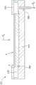
现在参考图3-4,通过使用结构夹持物11实现结构9的扩张。结构夹持物11包括顶板13。如在图3-4中所示,顶板13为环。顶板13可能具有其它形状并且可能跨衬底9完全地延伸而没有限制。顶板13适合于在结构的周向边缘5处接触衬底9的前表面。Referring now to FIGS. 3-4 , expansion of the
结构夹持物11包括用于邻近周向边缘5接触结构9的背表面的背板15。背板15包括外围环20,该外围环20向上延伸朝向顶板13。然而在其它实施例中,外围环20可能为顶板13的部分或可能与顶板13和背板15都分开。背板15、顶板13以及外围环20均适合于在顶板13、背板15(包括外围环)与结构9的周向边缘5之间形成外围腔18。通常,背板15和顶板13与结构9形成密封,该密封允许在外围腔18中的压力如在下文所描述的相对于夹持物11的外面的压力被减少。外围腔18被这样形成,通过在背板15上定位半导体结构9并且降低顶板13到背板15上直到在顶板13、背板15与结构9的周向边缘5之间形成密封。The
夹持物11包括在背板15中的出口22用于调整在外围腔18中的压力。备选地,出口通过前板13和/或外围环20延伸。出口22为与泵(未示出)流体连通用于减少在外围腔18中的压力。The
现在参考图8,夹持物11为用于扩张结构9的装置36的部分。装置36也包括壳35,该壳35限定主腔27,在该主腔27中设置有夹持物11。装置36包括出口32,该出口32与泵(未示出)流体连通用于调节在主腔中的压力P1。在结构夹持物11中的出口22通过壳35延伸。以这种方式,在主腔27中维持压力P1,而在结构夹持物11的外围腔18中维持不同的压力P2。通过将在主腔27中的压力P1维持为大于在外围腔18中的压力P2,结构9被扩张(即,增加衬底的半径)。Referring now to FIG. 8 , the
在此方面,在图3-15中的与压力P1和/或P2相关的箭头被提供用于示例性目的,而不应该被认为是限制装置为特定压力分布(即,在外围腔或主腔中的真空或压力的使用)。In this regard, the arrows associated with pressuresP1 and/orP2 in FIGS. 3-15 are provided for exemplary purposes and should not be considered as limiting means for a particular pressure use of vacuum or pressure in the main cavity).
在结构9的扩张中,P1为比P2大至少大约10MPa,或如在其它实施例中,比P2大至少大约20MPa、至少大约50MPa或至少大约75MPa(例如,从大约10MPa到大约100MPa、从大约10MPa到大约50MPa或从大约10MPa到大约25MPa)。在一些实施例中,P1为周围压力。在这样的实施例中,将主腔27和壳35消除并且将壳暴露到周围环境(即,大气压力)。In expansion of
在扩张期间将加热元件30用于加热结构9以激活位错源层。如上文所描述的,将结构加热到从大约650℃到大约1000℃或从大约700℃到大约1000℃的温度。A
在图5中示出结构夹持物111的另一实施例。应当指出,在图5中示出的夹持物部件类似于在图3中那些,通过图3的相应的参考数字加“100”而指定(例如,部件15变成部件115)。如在图5中所示,顶板113包括用于接触结构9的前表面8的突出物117。突出物117与结构9形成密封以允许增加或减少在外围腔118中的压力。Another embodiment of a
在一些实施例中并且如在图6-7中所示,在结构表面的至少部分上结构9具有涂层39(图6)或涂层40(图7)。如在图6中所示,涂层39越过结构9的周向边缘5与前表面8和背表面4的与邻近外围边缘5的部分而延伸。如在图7中所示,涂层40也越过结构的整个背表面4而延伸。备选地或附加地,涂层越过结构夹持物的一个或多个表面而延伸。涂层39或涂层40(或越过结构夹持物而延伸的涂层)由诸如石墨、六方氮化硼、MS2、WS2、SiCN、AlCr(V)N、TiAl(Y)N、CaF2、BaF2、SrF2或BaCrO4的低摩擦材料组成。在一些实施例中,在结构的前表面上,结构9具有涂层,其降低或甚至阻止结构的挥发膜部件的蒸发。用于降低蒸发的适合的涂层包括非晶硅。In some embodiments and as shown in FIGS. 6-7 ,
在图9中示出结构夹持物211的另一实施例。应当指出,在图9中示出的夹持物部件类似于在图3中那些,通过图3的相应的参考数字加“200”而指定(例如,部件15变成部件215)。结构夹持物211的顶板213包括凹陷,在结构夹持物211的使用期间,该凹陷适合于在顶板213与结构9的前表面8之间形成中心腔240。通过降低顶板213到半导体结构9上形成中心腔240。通过环形壁242限定凹陷。凹陷具有小于结构的应变半径的半径。如此处所使用,“应变半径”指的是在使用结构夹持物211的结构9的径向扩张(变形)之前的结构的半径。Another embodiment of a
顶板213包括出口246,该出口246与泵(未示出)流体连通以在中心腔240中维持压力P1。以这种方式,将压差维持在中心腔240与外围腔218之间以使得结构9被径向扩张。通过将在中心腔240中的压力P1维持为大于在外围腔218中的压力P2,结构被扩张。压力P1和/或P2为在上文描述的范围内。
在图11中示出用于径向扩张结构的自限制结构夹持物的实施例。在图11中示出的夹持物部件类似于在图3中那些,通过图3的相应的参考数字加“300”而指定。结构夹持物311的背板315包括通过环形壁352限定的适合于在结构的扩张期间限制结构的膨胀的凹陷。背板315的凹陷的半径大于结构的应变半径。在扩张期间,结构9的半径增长直到结构接触环形壁352。当接触环形壁352时,结构9的扩张停止。An embodiment of a self-limiting structure holder for a radially expanding structure is shown in FIG. 11 . The holder components shown in FIG. 11 are similar to those in FIG. 3 and are designated by the corresponding reference numerals of FIG. 3 plus "300". The
在图12中示出用于径向扩张结构9的自限制结构夹持物的另一实施例。在图12中示出的夹持物部件类似于在图3中那些,通过图3的相应的参考数字加“400”而指定。夹持物411包括在外围腔418中的穿孔壁455,该穿孔壁455适合于在结构9的扩张期间限制结构的膨胀。在壁455中形成的穿孔允许压力通过外围腔418而平衡。外围壁455在径向扩张期间限制结构9的扩张。Another embodiment of a self-limiting structure holder for a
在图13中示出用于径向扩张结构的自限制结构夹持物的另一实施例。在图13中示出的夹持物部件类似于在图3中那些,通过图3的相应的参考数字加“500”而指定。在使用之前,结构夹持物511的背板515的外围环520相对接近弛豫结构而延伸。在扩张期间,结构9径向扩张直到结构9接触外围环520以限制结构的扩张。Another embodiment of a self-limiting structure holder for a radially expanding structure is shown in FIG. 13 . The holder components shown in FIG. 13 are similar to those in FIG. 3 and are designated by the corresponding reference numerals of FIG. 3 plus "500". Prior to use, the
为了扩张(即,拉伸)结构9,备选地或除在主腔中使用较高压力之外,可使用压缩板659(图10)以向下施加结构的压力P1。在图10中示出的夹持物部件类似于在图3中那些,通过图3的相应的参考数字加“600”而指定。将压力P2维持在外围腔618中。P2小于P1以维持压差以扩张结构9。如上文所描述,P1为比P2大至少大约10MPa,或如在其它实施例中,比P2大至少大约20MPa、至少大约50MPa或至少大约75MPa(例如,从大约10MPa到大约100MPa、从大约10MPa到大约50MPa或从大约10MPa到大约25MPa)。通过任何适合的方法(诸如,通过水力学、气动或电驱动的使用),将力通过压缩板659施加到结构9。将上文描述的自限制特征与压缩板659结合使用。To expand (ie stretch) the
如在图14中所示,用于径向扩张结构的结构夹持物适合于同时地扩张多个结构。在图14中示出的夹持物部件类似于在图3中那些,通过图3的相应的参考数字加“700”而指定。夹持物711包括背板715,该背板715适合于邻近结构的周向边缘接触结构9a、9b、9c、9d。夹持物711包括顶板713,该顶板713邻近结构的周向边缘接触结构9a、9b、9c、9d。在背板715、顶板713与结构9a、9b、9c、9d的周向边缘之间形成外围腔718。顶板713包含腔760,该腔760延伸到结构9a、9b、9c、9d的前表面以允许结构被暴露到在主腔中(未示出)的压力P1。将外围腔718维持在压力P2。As shown in Figure 14, the structure holder for radially expanding structures is adapted to expand multiple structures simultaneously. The holder components shown in FIG. 14 are similar to those in FIG. 3 and are designated by the corresponding reference numerals of FIG. 3 plus "700". The
通过将P1维持为大于P2,径向扩张结构9a、9b、9c、9d。在P1与P2之间的差为至少大约10MPa,并且在上文描述的任何范围内。在这样的实施例中,P1为大气压力,并且顶板713为连续部分,没有包含分开腔760。当描述和示出在图14中示出的衬底夹持物仅具有一个背板和一个顶板时,应当理解,夹持物具有密封单个结构或结构的组合的多个分开的背或顶板。此外,当在图14中示出的衬底夹持物711能够径向扩张四个结构,应当指出,将夹持物设置为同时扩张或多或少的结构而没有限制。By maintainingP1 greater thanP2 , the
在图15中示出用于处理多个结构的自限制结构夹持物的实施例。在图15中示出的夹持物部件类似于在图3中那些,通过图3的相应的参考数字加“800”而指定。背板815包括适合于接收结构9a、9b、9c、9d的若干凹陷。通过环形壁852a、852b、852c、852d限定凹陷。环形壁852a、852b、852c、852d作为限制结构9a、9b、9c、9d的径向扩张。An embodiment of a self-limiting structure holder for handling multiple structures is shown in FIG. 15 . The holder components shown in FIG. 15 are similar to those in FIG. 3 and are designated by the corresponding reference numerals of FIG. 3 plus "800". The
除了上文描述的装置,紧握结构(诸如在外围边缘通过夹具或其他紧握元件的使用)并且允许结构被扩张(拉伸)的装置被用于弛豫诸如下文描述的在装置中的异质结构。现在参考图16-21,通过结构夹持物的使用实现结构的扩张,其相对结构为径向可移动的。在这样的实施例中,结构夹持物为装置的部分用于扩张结构。这样的装置类似于在图8中示出的装置36,装置包括壳35,该壳35限定主腔27,在该主腔27中设置夹持物。装置包括加热元件30以在扩张期间通过图16-21的结构的任何的使用加热结构9以激活位错源层。In addition to the devices described above, devices that grasp the structure (such as through the use of clamps or other grasping elements at the peripheral edges) and allow the structure to be expanded (stretched) are used to relax heterogeneity in devices such as those described below. qualitative structure. Referring now to Figures 16-21, expansion of the structure is achieved through the use of structure holders, which are radially movable relative to the structure. In such embodiments, the structural holder is part of the device for expanding the structure. Such a device is similar to the
现在参考图16,结构夹持物1720包括多个三角形状的段1785,其向内指向夹持物的中心轴A。每个段具有在其中形成的至少一个流体通道1787以在衬底上拉真空。段1785被设置用于从中心轴A向外移动使得衬底被扩张。Referring now to FIG. 16, the
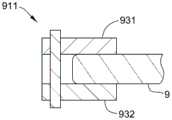
现在参考图17,装置911为夹具,其包括前板931和背板932,其对衬底9施加夹持力。如在图17中所示,顶板931和背板932为环。顶板931可能具有其它形状并且可能跨衬底9完全地延伸而没有限制。通过包括使用气动、水力学、发动机等等的任何机械方法,前板931和背板932为从装置的中心向外径向可移动的。应当指出,将这样的机械方法用于移动下文描述的结构夹持物中的任何前板和/或背板。Referring now to FIG. 17 , the
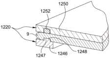
现在参考图18,在另一实施例中,结构夹持物1011包括通常平坦的背板1146,其包括环形凸台1147,该环形凸台1147被改变且成形以被在结构9的背面中的槽1148中接收。凸台1147为可移动的以便其扩张结构9。Referring now to FIG. 18 , in another embodiment, the
在一些实施例中且如在图19中所示,结构夹持物1220也包括前板1250,该前板1250具有从前板延伸的环形环1252。在加热期间,环1252对结构9施加向下力以在结构的扩张期间阻止结构从凸台1247松脱。用于完成该功能的其它结构在本公开内容的范围内为预期的。In some embodiments and as shown in FIG. 19 , the
在其它实施例中且如在图20中所示,结构夹持物1320包括类似于或相同于在图18和19中所示的背板1346和凸台1347。衬底夹持物1320也包括前板1351和前凸台1355,其被改变且成形以被在结构9的前表面中的槽1357中接收。In other embodiments and as shown in FIG. 20 , the
参考图21,结构夹持物1620包括通常平坦的背板1681和凸缘1683。结构9包括附着到邻近结构的外围边缘的结构的背表面的环1680。凸缘1683适合于啮合环1680。支撑1681和凸缘1683相对结构为可移动的以扩张结构。Referring to FIG. 21 , the
在一些实施例中,通过上文描述的装置施加的应力为循环的,诸如通过降低跨结构的压差(例如,通过减少或增加在外围或主腔中的压力)或通过降低在装置紧握衬底的实施例中施加的应力。这样的循环释放在结构中形成的任何弹性应力。In some embodiments, the stress applied by the devices described above is cyclic, such as by reducing the pressure differential across the structure (e.g., by reducing or increasing the pressure in the peripheral or main lumen) or by reducing the pressure on the device when gripped. Example of substrate applied stress. Such cycling relieves any elastic stresses built up in the structure.
如此处所使用,当术语“大约”、“基本上”、“实质上”以及“近似”被用于结合尺寸、浓度、温度或其它物理或化学性质或特性的范围时旨在覆盖出现在性质或特性的范围的上限和/或下限的变化,包括,例如,从四舍五入、测量方法学或其它统计变化产生的变化。As used herein, the terms "about", "substantially", "substantially" and "approximately" when used in conjunction with a range of size, concentration, temperature or other physical or chemical property or characteristic are intended to cover Variations in the upper and/or lower limits of a range for a property, including, for example, changes resulting from rounding, measurement methodology, or other statistical changes.
当介绍本公开内容或及其优选的实施例的元件时,冠词“一”、“一个”、“该”以及“所述”旨在是指一个或多个的元件。术语“包括”、“包含”以及“具有”旨在包容性且旨在具有除了列出的元件还可具有附加的元件。When introducing elements of the present disclosure or preferred embodiments thereof, the articles "a", "an", "the" and "said" are intended to refer to one or more of the elements. The terms "comprising", "comprising" and "having" are intended to be inclusive and are intended to have additional elements other than the listed elements.
可以做出没有脱离本公开内容的范围的在上文中的装置和方法的各种变化,旨在在上文的说明书中包含且在附图中示出的所有事物应该被解释为阐述性的而非限制性的意义。As various changes could be made in the above devices and methods without departing from the scope of the disclosure, it is intended that all matter contained in the above description and shown in the accompanying drawings shall be interpreted as illustrative and not as non-limiting meaning.
Claims (13)
Priority Applications (1)
| Application Number | Priority Date | Filing Date | Title |
|---|---|---|---|
| CN201810030851.9ACN107968067B (en) | 2012-12-31 | 2013-12-30 | Method and apparatus for fabricating heterostructures with reduced strain by radial expansion |
Applications Claiming Priority (11)
| Application Number | Priority Date | Filing Date | Title |
|---|---|---|---|
| US201261747613P | 2012-12-31 | 2012-12-31 | |
| US61/747,613 | 2012-12-31 | ||
| US201361788744P | 2013-03-15 | 2013-03-15 | |
| US201361790445P | 2013-03-15 | 2013-03-15 | |
| US201361793999P | 2013-03-15 | 2013-03-15 | |
| US61/788,744 | 2013-03-15 | ||
| US61/793,999 | 2013-03-15 | ||
| US61/790,445 | 2013-03-15 | ||
| PCT/US2013/078224WO2014106155A2 (en) | 2012-12-31 | 2013-12-30 | Processes and apparatus for preparing heterostructures with reduced strain by radial distension |
| CN201810030851.9ACN107968067B (en) | 2012-12-31 | 2013-12-30 | Method and apparatus for fabricating heterostructures with reduced strain by radial expansion |
| CN201380073264.3ACN105144341B (en) | 2012-12-31 | 2013-12-30 | Method and apparatus for fabricating heterostructures with reduced strain by radial expansion |
Related Parent Applications (1)
| Application Number | Title | Priority Date | Filing Date |
|---|---|---|---|
| CN201380073264.3ADivisionCN105144341B (en) | 2012-12-31 | 2013-12-30 | Method and apparatus for fabricating heterostructures with reduced strain by radial expansion |
Publications (2)
| Publication Number | Publication Date |
|---|---|
| CN107968067A CN107968067A (en) | 2018-04-27 |
| CN107968067Btrue CN107968067B (en) | 2023-05-26 |
Family
ID=49958756
Family Applications (5)
| Application Number | Title | Priority Date | Filing Date |
|---|---|---|---|
| CN201810030851.9AActiveCN107968067B (en) | 2012-12-31 | 2013-12-30 | Method and apparatus for fabricating heterostructures with reduced strain by radial expansion |
| CN201380073273.2AActiveCN105210172B (en) | 2012-12-31 | 2013-12-30 | Method and apparatus for fabricating heterostructures with reduced strain by radial compression |
| CN201380073264.3AActiveCN105144341B (en) | 2012-12-31 | 2013-12-30 | Method and apparatus for fabricating heterostructures with reduced strain by radial expansion |
| CN202310507878.3APendingCN116544172A (en) | 2012-12-31 | 2013-12-30 | Method and apparatus for preparing heterostructures with strain reduction by radial compression |
| CN201810287918.7AActiveCN108336013B (en) | 2012-12-31 | 2013-12-30 | Method and apparatus for preparing heterostructures with strain reduction by radial compression |
Family Applications After (4)
| Application Number | Title | Priority Date | Filing Date |
|---|---|---|---|
| CN201380073273.2AActiveCN105210172B (en) | 2012-12-31 | 2013-12-30 | Method and apparatus for fabricating heterostructures with reduced strain by radial compression |
| CN201380073264.3AActiveCN105144341B (en) | 2012-12-31 | 2013-12-30 | Method and apparatus for fabricating heterostructures with reduced strain by radial expansion |
| CN202310507878.3APendingCN116544172A (en) | 2012-12-31 | 2013-12-30 | Method and apparatus for preparing heterostructures with strain reduction by radial compression |
| CN201810287918.7AActiveCN108336013B (en) | 2012-12-31 | 2013-12-30 | Method and apparatus for preparing heterostructures with strain reduction by radial compression |
Country Status (7)
| Country | Link |
|---|---|
| US (7) | US9583363B2 (en) |
| EP (6) | EP3188224B1 (en) |
| JP (10) | JP6314153B2 (en) |
| KR (2) | KR102203560B1 (en) |
| CN (5) | CN107968067B (en) |
| TW (4) | TWI673865B (en) |
| WO (3) | WO2014106177A1 (en) |
Families Citing this family (266)
| Publication number | Priority date | Publication date | Assignee | Title |
|---|---|---|---|---|
| US20130023129A1 (en) | 2011-07-20 | 2013-01-24 | Asm America, Inc. | Pressure transmitter for a semiconductor processing environment |
| US10714315B2 (en) | 2012-10-12 | 2020-07-14 | Asm Ip Holdings B.V. | Semiconductor reaction chamber showerhead |
| US9583363B2 (en)* | 2012-12-31 | 2017-02-28 | Sunedison Semiconductor Limited (Uen201334164H) | Processes and apparatus for preparing heterostructures with reduced strain by radial distension |
| US20160376700A1 (en) | 2013-02-01 | 2016-12-29 | Asm Ip Holding B.V. | System for treatment of deposition reactor |
| WO2014191624A1 (en)* | 2013-05-29 | 2014-12-04 | Beneq Oy | Substrate holder and arrangement for holding substrates |
| WO2014191621A1 (en)* | 2013-05-29 | 2014-12-04 | Beneq Oy | Substrate carrier and arrangement for supporting substrates |
| US10941490B2 (en) | 2014-10-07 | 2021-03-09 | Asm Ip Holding B.V. | Multiple temperature range susceptor, assembly, reactor and system including the susceptor, and methods of using the same |
| US10276355B2 (en) | 2015-03-12 | 2019-04-30 | Asm Ip Holding B.V. | Multi-zone reactor, system including the reactor, and method of using the same |
| US10458018B2 (en) | 2015-06-26 | 2019-10-29 | Asm Ip Holding B.V. | Structures including metal carbide material, devices including the structures, and methods of forming same |
| US10211308B2 (en) | 2015-10-21 | 2019-02-19 | Asm Ip Holding B.V. | NbMC layers |
| DE102015223807A1 (en)* | 2015-12-01 | 2017-06-01 | Siltronic Ag | Process for producing a semiconductor wafer with epitaxial layer in a deposition chamber, apparatus for producing an epitaxial-layer semiconductor wafer and semiconductor wafer with epitaxial layer |
| US11139308B2 (en) | 2015-12-29 | 2021-10-05 | Asm Ip Holding B.V. | Atomic layer deposition of III-V compounds to form V-NAND devices |
| US10529554B2 (en) | 2016-02-19 | 2020-01-07 | Asm Ip Holding B.V. | Method for forming silicon nitride film selectively on sidewalls or flat surfaces of trenches |
| US10343920B2 (en) | 2016-03-18 | 2019-07-09 | Asm Ip Holding B.V. | Aligned carbon nanotubes |
| US11453943B2 (en) | 2016-05-25 | 2022-09-27 | Asm Ip Holding B.V. | Method for forming carbon-containing silicon/metal oxide or nitride film by ALD using silicon precursor and hydrocarbon precursor |
| US10612137B2 (en) | 2016-07-08 | 2020-04-07 | Asm Ip Holdings B.V. | Organic reactants for atomic layer deposition |
| US9859151B1 (en) | 2016-07-08 | 2018-01-02 | Asm Ip Holding B.V. | Selective film deposition method to form air gaps |
| CN107623028B (en)* | 2016-07-13 | 2021-02-19 | 环球晶圆股份有限公司 | Semiconductor substrate and processing method thereof |
| US9887082B1 (en) | 2016-07-28 | 2018-02-06 | Asm Ip Holding B.V. | Method and apparatus for filling a gap |
| US9812320B1 (en) | 2016-07-28 | 2017-11-07 | Asm Ip Holding B.V. | Method and apparatus for filling a gap |
| CN109564868B (en)* | 2016-08-25 | 2023-04-04 | 日本瑞翁株式会社 | Plasma etching method |
| US11532757B2 (en) | 2016-10-27 | 2022-12-20 | Asm Ip Holding B.V. | Deposition of charge trapping layers |
| US10714350B2 (en) | 2016-11-01 | 2020-07-14 | ASM IP Holdings, B.V. | Methods for forming a transition metal niobium nitride film on a substrate by atomic layer deposition and related semiconductor device structures |
| KR102546317B1 (en) | 2016-11-15 | 2023-06-21 | 에이에스엠 아이피 홀딩 비.브이. | Gas supply unit and substrate processing apparatus including the same |
| KR102762543B1 (en) | 2016-12-14 | 2025-02-05 | 에이에스엠 아이피 홀딩 비.브이. | Substrate processing apparatus |
| US11581186B2 (en) | 2016-12-15 | 2023-02-14 | Asm Ip Holding B.V. | Sequential infiltration synthesis apparatus |
| US11447861B2 (en) | 2016-12-15 | 2022-09-20 | Asm Ip Holding B.V. | Sequential infiltration synthesis apparatus and a method of forming a patterned structure |
| US10269558B2 (en) | 2016-12-22 | 2019-04-23 | Asm Ip Holding B.V. | Method of forming a structure on a substrate |
| US10068787B2 (en)* | 2016-12-30 | 2018-09-04 | Sunpower Corporation | Bowing semiconductor wafers |
| US11390950B2 (en) | 2017-01-10 | 2022-07-19 | Asm Ip Holding B.V. | Reactor system and method to reduce residue buildup during a film deposition process |
| US10468261B2 (en) | 2017-02-15 | 2019-11-05 | Asm Ip Holding B.V. | Methods for forming a metallic film on a substrate by cyclical deposition and related semiconductor device structures |
| US10770286B2 (en) | 2017-05-08 | 2020-09-08 | Asm Ip Holdings B.V. | Methods for selectively forming a silicon nitride film on a substrate and related semiconductor device structures |
| KR102015336B1 (en)* | 2017-06-12 | 2019-08-28 | 삼성전자주식회사 | Method of reducing warpage of semiconductor package substrate and warpage reducer device |
| US12040200B2 (en) | 2017-06-20 | 2024-07-16 | Asm Ip Holding B.V. | Semiconductor processing apparatus and methods for calibrating a semiconductor processing apparatus |
| US11306395B2 (en) | 2017-06-28 | 2022-04-19 | Asm Ip Holding B.V. | Methods for depositing a transition metal nitride film on a substrate by atomic layer deposition and related deposition apparatus |
| KR20190009245A (en) | 2017-07-18 | 2019-01-28 | 에이에스엠 아이피 홀딩 비.브이. | Methods for forming a semiconductor device structure and related semiconductor device structures |
| US11374112B2 (en) | 2017-07-19 | 2022-06-28 | Asm Ip Holding B.V. | Method for depositing a group IV semiconductor and related semiconductor device structures |
| US10590535B2 (en) | 2017-07-26 | 2020-03-17 | Asm Ip Holdings B.V. | Chemical treatment, deposition and/or infiltration apparatus and method for using the same |
| TWI815813B (en) | 2017-08-04 | 2023-09-21 | 荷蘭商Asm智慧財產控股公司 | Showerhead assembly for distributing a gas within a reaction chamber |
| US10692741B2 (en) | 2017-08-08 | 2020-06-23 | Asm Ip Holdings B.V. | Radiation shield |
| US10770336B2 (en) | 2017-08-08 | 2020-09-08 | Asm Ip Holding B.V. | Substrate lift mechanism and reactor including same |
| US11769682B2 (en) | 2017-08-09 | 2023-09-26 | Asm Ip Holding B.V. | Storage apparatus for storing cassettes for substrates and processing apparatus equipped therewith |
| US11830730B2 (en) | 2017-08-29 | 2023-11-28 | Asm Ip Holding B.V. | Layer forming method and apparatus |
| US11295980B2 (en) | 2017-08-30 | 2022-04-05 | Asm Ip Holding B.V. | Methods for depositing a molybdenum metal film over a dielectric surface of a substrate by a cyclical deposition process and related semiconductor device structures |
| US10658205B2 (en) | 2017-09-28 | 2020-05-19 | Asm Ip Holdings B.V. | Chemical dispensing apparatus and methods for dispensing a chemical to a reaction chamber |
| US10403504B2 (en) | 2017-10-05 | 2019-09-03 | Asm Ip Holding B.V. | Method for selectively depositing a metallic film on a substrate |
| US10923344B2 (en) | 2017-10-30 | 2021-02-16 | Asm Ip Holding B.V. | Methods for forming a semiconductor structure and related semiconductor structures |
| WO2019103613A1 (en) | 2017-11-27 | 2019-05-31 | Asm Ip Holding B.V. | A storage device for storing wafer cassettes for use with a batch furnace |
| CN111344522B (en) | 2017-11-27 | 2022-04-12 | 阿斯莫Ip控股公司 | Including clean mini-environment device |
| US10872771B2 (en) | 2018-01-16 | 2020-12-22 | Asm Ip Holding B. V. | Method for depositing a material film on a substrate within a reaction chamber by a cyclical deposition process and related device structures |
| TWI799494B (en) | 2018-01-19 | 2023-04-21 | 荷蘭商Asm 智慧財產控股公司 | Deposition method |
| KR102695659B1 (en) | 2018-01-19 | 2024-08-14 | 에이에스엠 아이피 홀딩 비.브이. | Method for depositing a gap filling layer by plasma assisted deposition |
| US11081345B2 (en) | 2018-02-06 | 2021-08-03 | Asm Ip Holding B.V. | Method of post-deposition treatment for silicon oxide film |
| US10896820B2 (en) | 2018-02-14 | 2021-01-19 | Asm Ip Holding B.V. | Method for depositing a ruthenium-containing film on a substrate by a cyclical deposition process |
| WO2019158960A1 (en) | 2018-02-14 | 2019-08-22 | Asm Ip Holding B.V. | A method for depositing a ruthenium-containing film on a substrate by a cyclical deposition process |
| US10731249B2 (en) | 2018-02-15 | 2020-08-04 | Asm Ip Holding B.V. | Method of forming a transition metal containing film on a substrate by a cyclical deposition process, a method for supplying a transition metal halide compound to a reaction chamber, and related vapor deposition apparatus |
| KR102636427B1 (en) | 2018-02-20 | 2024-02-13 | 에이에스엠 아이피 홀딩 비.브이. | Substrate processing method and apparatus |
| US10975470B2 (en) | 2018-02-23 | 2021-04-13 | Asm Ip Holding B.V. | Apparatus for detecting or monitoring for a chemical precursor in a high temperature environment |
| US11473195B2 (en) | 2018-03-01 | 2022-10-18 | Asm Ip Holding B.V. | Semiconductor processing apparatus and a method for processing a substrate |
| US11629406B2 (en) | 2018-03-09 | 2023-04-18 | Asm Ip Holding B.V. | Semiconductor processing apparatus comprising one or more pyrometers for measuring a temperature of a substrate during transfer of the substrate |
| KR102646467B1 (en) | 2018-03-27 | 2024-03-11 | 에이에스엠 아이피 홀딩 비.브이. | Method of forming an electrode on a substrate and a semiconductor device structure including an electrode |
| US11230766B2 (en) | 2018-03-29 | 2022-01-25 | Asm Ip Holding B.V. | Substrate processing apparatus and method |
| KR102600229B1 (en) | 2018-04-09 | 2023-11-10 | 에이에스엠 아이피 홀딩 비.브이. | Substrate supporting device, substrate processing apparatus including the same and substrate processing method |
| US12025484B2 (en) | 2018-05-08 | 2024-07-02 | Asm Ip Holding B.V. | Thin film forming method |
| TWI811348B (en) | 2018-05-08 | 2023-08-11 | 荷蘭商Asm 智慧財產控股公司 | Methods for depositing an oxide film on a substrate by a cyclical deposition process and related device structures |
| US12272527B2 (en) | 2018-05-09 | 2025-04-08 | Asm Ip Holding B.V. | Apparatus for use with hydrogen radicals and method of using same |
| KR102596988B1 (en) | 2018-05-28 | 2023-10-31 | 에이에스엠 아이피 홀딩 비.브이. | Method of processing a substrate and a device manufactured by the same |
| US11201079B2 (en)* | 2018-05-30 | 2021-12-14 | Taiwan Semiconductor Manufacturing Company, Ltd. | Wafer chuck |
| US11718913B2 (en) | 2018-06-04 | 2023-08-08 | Asm Ip Holding B.V. | Gas distribution system and reactor system including same |
| TWI840362B (en) | 2018-06-04 | 2024-05-01 | 荷蘭商Asm Ip私人控股有限公司 | Wafer handling chamber with moisture reduction |
| US11286562B2 (en) | 2018-06-08 | 2022-03-29 | Asm Ip Holding B.V. | Gas-phase chemical reactor and method of using same |
| KR102568797B1 (en) | 2018-06-21 | 2023-08-21 | 에이에스엠 아이피 홀딩 비.브이. | Substrate processing system |
| US10797133B2 (en) | 2018-06-21 | 2020-10-06 | Asm Ip Holding B.V. | Method for depositing a phosphorus doped silicon arsenide film and related semiconductor device structures |
| KR102854019B1 (en) | 2018-06-27 | 2025-09-02 | 에이에스엠 아이피 홀딩 비.브이. | Periodic deposition method for forming a metal-containing material and films and structures comprising the metal-containing material |
| TWI873894B (en) | 2018-06-27 | 2025-02-21 | 荷蘭商Asm Ip私人控股有限公司 | Cyclic deposition methods for forming metal-containing material and films and structures including the metal-containing material |
| US10612136B2 (en) | 2018-06-29 | 2020-04-07 | ASM IP Holding, B.V. | Temperature-controlled flange and reactor system including same |
| US10755922B2 (en) | 2018-07-03 | 2020-08-25 | Asm Ip Holding B.V. | Method for depositing silicon-free carbon-containing film as gap-fill layer by pulse plasma-assisted deposition |
| US10388513B1 (en) | 2018-07-03 | 2019-08-20 | Asm Ip Holding B.V. | Method for depositing silicon-free carbon-containing film as gap-fill layer by pulse plasma-assisted deposition |
| US11430674B2 (en) | 2018-08-22 | 2022-08-30 | Asm Ip Holding B.V. | Sensor array, apparatus for dispensing a vapor phase reactant to a reaction chamber and related methods |
| US11024523B2 (en) | 2018-09-11 | 2021-06-01 | Asm Ip Holding B.V. | Substrate processing apparatus and method |
| KR102707956B1 (en) | 2018-09-11 | 2024-09-19 | 에이에스엠 아이피 홀딩 비.브이. | Method for deposition of a thin film |
| CN110970344B (en) | 2018-10-01 | 2024-10-25 | Asmip控股有限公司 | Substrate holding apparatus, system comprising the same and method of using the same |
| US11232963B2 (en) | 2018-10-03 | 2022-01-25 | Asm Ip Holding B.V. | Substrate processing apparatus and method |
| KR102592699B1 (en) | 2018-10-08 | 2023-10-23 | 에이에스엠 아이피 홀딩 비.브이. | Substrate support unit and apparatuses for depositing thin film and processing the substrate including the same |
| KR102546322B1 (en) | 2018-10-19 | 2023-06-21 | 에이에스엠 아이피 홀딩 비.브이. | Substrate processing apparatus and substrate processing method |
| KR102605121B1 (en) | 2018-10-19 | 2023-11-23 | 에이에스엠 아이피 홀딩 비.브이. | Substrate processing apparatus and substrate processing method |
| US12378665B2 (en) | 2018-10-26 | 2025-08-05 | Asm Ip Holding B.V. | High temperature coatings for a preclean and etch apparatus and related methods |
| US11087997B2 (en) | 2018-10-31 | 2021-08-10 | Asm Ip Holding B.V. | Substrate processing apparatus for processing substrates |
| KR102748291B1 (en) | 2018-11-02 | 2024-12-31 | 에이에스엠 아이피 홀딩 비.브이. | Substrate support unit and substrate processing apparatus including the same |
| US11572620B2 (en) | 2018-11-06 | 2023-02-07 | Asm Ip Holding B.V. | Methods for selectively depositing an amorphous silicon film on a substrate |
| US10818758B2 (en) | 2018-11-16 | 2020-10-27 | Asm Ip Holding B.V. | Methods for forming a metal silicate film on a substrate in a reaction chamber and related semiconductor device structures |
| US12040199B2 (en) | 2018-11-28 | 2024-07-16 | Asm Ip Holding B.V. | Substrate processing apparatus for processing substrates |
| US11217444B2 (en) | 2018-11-30 | 2022-01-04 | Asm Ip Holding B.V. | Method for forming an ultraviolet radiation responsive metal oxide-containing film |
| KR102636428B1 (en) | 2018-12-04 | 2024-02-13 | 에이에스엠 아이피 홀딩 비.브이. | A method for cleaning a substrate processing apparatus |
| US11158513B2 (en) | 2018-12-13 | 2021-10-26 | Asm Ip Holding B.V. | Methods for forming a rhenium-containing film on a substrate by a cyclical deposition process and related semiconductor device structures |
| TWI874340B (en) | 2018-12-14 | 2025-03-01 | 荷蘭商Asm Ip私人控股有限公司 | Method of forming device structure, structure formed by the method and system for performing the method |
| TWI866480B (en) | 2019-01-17 | 2024-12-11 | 荷蘭商Asm Ip 私人控股有限公司 | Methods of forming a transition metal containing film on a substrate by a cyclical deposition process |
| KR102727227B1 (en) | 2019-01-22 | 2024-11-07 | 에이에스엠 아이피 홀딩 비.브이. | Semiconductor processing device |
| TWI838458B (en)* | 2019-02-20 | 2024-04-11 | 荷蘭商Asm Ip私人控股有限公司 | Apparatus and methods for plug fill deposition in 3-d nand applications |
| TWI845607B (en) | 2019-02-20 | 2024-06-21 | 荷蘭商Asm Ip私人控股有限公司 | Cyclical deposition method and apparatus for filling a recess formed within a substrate surface |
| KR102626263B1 (en) | 2019-02-20 | 2024-01-16 | 에이에스엠 아이피 홀딩 비.브이. | Cyclical deposition method including treatment step and apparatus for same |
| TWI873122B (en) | 2019-02-20 | 2025-02-21 | 荷蘭商Asm Ip私人控股有限公司 | Method of filling a recess formed within a surface of a substrate, semiconductor structure formed according to the method, and semiconductor processing apparatus |
| TWI842826B (en) | 2019-02-22 | 2024-05-21 | 荷蘭商Asm Ip私人控股有限公司 | Substrate processing apparatus and method for processing substrate |
| KR102858005B1 (en) | 2019-03-08 | 2025-09-09 | 에이에스엠 아이피 홀딩 비.브이. | Method for Selective Deposition of Silicon Nitride Layer and Structure Including Selectively-Deposited Silicon Nitride Layer |
| US11742198B2 (en) | 2019-03-08 | 2023-08-29 | Asm Ip Holding B.V. | Structure including SiOCN layer and method of forming same |
| KR102673983B1 (en)* | 2019-03-15 | 2024-06-12 | 주식회사 케이씨텍 | Apparatus for Treating Substrate |
| JP7279465B2 (en)* | 2019-03-28 | 2023-05-23 | 住友金属鉱山株式会社 | SUPPORTING SUBSTRATE, SUPPORTING SUBSTRATE HOLDING METHOD, AND FILM-FORMING METHOD |
| JP2020167398A (en) | 2019-03-28 | 2020-10-08 | エーエスエム・アイピー・ホールディング・ベー・フェー | Door openers and substrate processing equipment provided with door openers |
| KR102809999B1 (en) | 2019-04-01 | 2025-05-19 | 에이에스엠 아이피 홀딩 비.브이. | Method of manufacturing semiconductor device |
| KR20200123380A (en) | 2019-04-19 | 2020-10-29 | 에이에스엠 아이피 홀딩 비.브이. | Layer forming method and apparatus |
| KR20200125453A (en) | 2019-04-24 | 2020-11-04 | 에이에스엠 아이피 홀딩 비.브이. | Gas-phase reactor system and method of using same |
| KR20200130121A (en) | 2019-05-07 | 2020-11-18 | 에이에스엠 아이피 홀딩 비.브이. | Chemical source vessel with dip tube |
| US11289326B2 (en) | 2019-05-07 | 2022-03-29 | Asm Ip Holding B.V. | Method for reforming amorphous carbon polymer film |
| KR20200130652A (en) | 2019-05-10 | 2020-11-19 | 에이에스엠 아이피 홀딩 비.브이. | Method of depositing material onto a surface and structure formed according to the method |
| JP7612342B2 (en) | 2019-05-16 | 2025-01-14 | エーエスエム・アイピー・ホールディング・ベー・フェー | Wafer boat handling apparatus, vertical batch furnace and method |
| JP7598201B2 (en) | 2019-05-16 | 2024-12-11 | エーエスエム・アイピー・ホールディング・ベー・フェー | Wafer boat handling apparatus, vertical batch furnace and method |
| USD975665S1 (en) | 2019-05-17 | 2023-01-17 | Asm Ip Holding B.V. | Susceptor shaft |
| USD947913S1 (en) | 2019-05-17 | 2022-04-05 | Asm Ip Holding B.V. | Susceptor shaft |
| KR20200141002A (en) | 2019-06-06 | 2020-12-17 | 에이에스엠 아이피 홀딩 비.브이. | Method of using a gas-phase reactor system including analyzing exhausted gas |
| KR20200141931A (en) | 2019-06-10 | 2020-12-21 | 에이에스엠 아이피 홀딩 비.브이. | Method for cleaning quartz epitaxial chambers |
| KR20200143254A (en) | 2019-06-11 | 2020-12-23 | 에이에스엠 아이피 홀딩 비.브이. | Method of forming an electronic structure using an reforming gas, system for performing the method, and structure formed using the method |
| USD944946S1 (en) | 2019-06-14 | 2022-03-01 | Asm Ip Holding B.V. | Shower plate |
| KR20210005515A (en) | 2019-07-03 | 2021-01-14 | 에이에스엠 아이피 홀딩 비.브이. | Temperature control assembly for substrate processing apparatus and method of using same |
| JP7499079B2 (en) | 2019-07-09 | 2024-06-13 | エーエスエム・アイピー・ホールディング・ベー・フェー | Plasma device using coaxial waveguide and substrate processing method |
| CN112216646A (en) | 2019-07-10 | 2021-01-12 | Asm Ip私人控股有限公司 | Substrate supporting assembly and substrate processing device comprising same |
| KR20210010307A (en) | 2019-07-16 | 2021-01-27 | 에이에스엠 아이피 홀딩 비.브이. | Substrate processing apparatus |
| KR102860110B1 (en) | 2019-07-17 | 2025-09-16 | 에이에스엠 아이피 홀딩 비.브이. | Methods of forming silicon germanium structures |
| KR20210010816A (en) | 2019-07-17 | 2021-01-28 | 에이에스엠 아이피 홀딩 비.브이. | Radical assist ignition plasma system and method |
| US11643724B2 (en) | 2019-07-18 | 2023-05-09 | Asm Ip Holding B.V. | Method of forming structures using a neutral beam |
| TWI839544B (en) | 2019-07-19 | 2024-04-21 | 荷蘭商Asm Ip私人控股有限公司 | Method of forming topology-controlled amorphous carbon polymer film |
| KR20210010817A (en) | 2019-07-19 | 2021-01-28 | 에이에스엠 아이피 홀딩 비.브이. | Method of Forming Topology-Controlled Amorphous Carbon Polymer Film |
| TWI851767B (en) | 2019-07-29 | 2024-08-11 | 荷蘭商Asm Ip私人控股有限公司 | Methods for selective deposition utilizing n-type dopants and/or alternative dopants to achieve high dopant incorporation |
| CN112309900A (en) | 2019-07-30 | 2021-02-02 | Asm Ip私人控股有限公司 | Substrate processing apparatus |
| CN112309899A (en) | 2019-07-30 | 2021-02-02 | Asm Ip私人控股有限公司 | Substrate processing apparatus |
| US12169361B2 (en) | 2019-07-30 | 2024-12-17 | Asm Ip Holding B.V. | Substrate processing apparatus and method |
| US11587815B2 (en) | 2019-07-31 | 2023-02-21 | Asm Ip Holding B.V. | Vertical batch furnace assembly |
| US11227782B2 (en) | 2019-07-31 | 2022-01-18 | Asm Ip Holding B.V. | Vertical batch furnace assembly |
| US11587814B2 (en) | 2019-07-31 | 2023-02-21 | Asm Ip Holding B.V. | Vertical batch furnace assembly |
| CN112323048B (en) | 2019-08-05 | 2024-02-09 | Asm Ip私人控股有限公司 | Liquid level sensor for chemical source container |
| CN112342526A (en) | 2019-08-09 | 2021-02-09 | Asm Ip私人控股有限公司 | Heater assembly including cooling device and method of using same |
| USD965524S1 (en) | 2019-08-19 | 2022-10-04 | Asm Ip Holding B.V. | Susceptor support |
| USD965044S1 (en) | 2019-08-19 | 2022-09-27 | Asm Ip Holding B.V. | Susceptor shaft |
| JP2021031769A (en) | 2019-08-21 | 2021-03-01 | エーエスエム アイピー ホールディング ビー.ブイ. | Production apparatus of mixed gas of film deposition raw material and film deposition apparatus |
| USD979506S1 (en) | 2019-08-22 | 2023-02-28 | Asm Ip Holding B.V. | Insulator |
| KR20210024423A (en) | 2019-08-22 | 2021-03-05 | 에이에스엠 아이피 홀딩 비.브이. | Method for forming a structure with a hole |
| USD949319S1 (en) | 2019-08-22 | 2022-04-19 | Asm Ip Holding B.V. | Exhaust duct |
| USD940837S1 (en) | 2019-08-22 | 2022-01-11 | Asm Ip Holding B.V. | Electrode |
| KR20210024420A (en) | 2019-08-23 | 2021-03-05 | 에이에스엠 아이피 홀딩 비.브이. | Method for depositing silicon oxide film having improved quality by peald using bis(diethylamino)silane |
| US11286558B2 (en) | 2019-08-23 | 2022-03-29 | Asm Ip Holding B.V. | Methods for depositing a molybdenum nitride film on a surface of a substrate by a cyclical deposition process and related semiconductor device structures including a molybdenum nitride film |
| KR102806450B1 (en) | 2019-09-04 | 2025-05-12 | 에이에스엠 아이피 홀딩 비.브이. | Methods for selective deposition using a sacrificial capping layer |
| KR102733104B1 (en) | 2019-09-05 | 2024-11-22 | 에이에스엠 아이피 홀딩 비.브이. | Substrate processing apparatus |
| US11562901B2 (en) | 2019-09-25 | 2023-01-24 | Asm Ip Holding B.V. | Substrate processing method |
| CN112593212B (en) | 2019-10-02 | 2023-12-22 | Asm Ip私人控股有限公司 | Method for forming topologically selective silicon oxide film by cyclic plasma enhanced deposition process |
| TWI846953B (en) | 2019-10-08 | 2024-07-01 | 荷蘭商Asm Ip私人控股有限公司 | Substrate processing device |
| KR20210042810A (en) | 2019-10-08 | 2021-04-20 | 에이에스엠 아이피 홀딩 비.브이. | Reactor system including a gas distribution assembly for use with activated species and method of using same |
| TW202128273A (en) | 2019-10-08 | 2021-08-01 | 荷蘭商Asm Ip私人控股有限公司 | Gas injection system, reactor system, and method of depositing material on surface of substratewithin reaction chamber |
| TWI846966B (en) | 2019-10-10 | 2024-07-01 | 荷蘭商Asm Ip私人控股有限公司 | Method of forming a photoresist underlayer and structure including same |
| US12009241B2 (en) | 2019-10-14 | 2024-06-11 | Asm Ip Holding B.V. | Vertical batch furnace assembly with detector to detect cassette |
| TWI834919B (en) | 2019-10-16 | 2024-03-11 | 荷蘭商Asm Ip私人控股有限公司 | Method of topology-selective film formation of silicon oxide |
| US11637014B2 (en) | 2019-10-17 | 2023-04-25 | Asm Ip Holding B.V. | Methods for selective deposition of doped semiconductor material |
| KR102845724B1 (en) | 2019-10-21 | 2025-08-13 | 에이에스엠 아이피 홀딩 비.브이. | Apparatus and methods for selectively etching films |
| US11328944B2 (en)* | 2019-10-23 | 2022-05-10 | Eugenus, Inc. | Systems and methods of placing substrates in semiconductor manufacturing equipment |
| KR20210050453A (en) | 2019-10-25 | 2021-05-07 | 에이에스엠 아이피 홀딩 비.브이. | Methods for filling a gap feature on a substrate surface and related semiconductor structures |
| US11646205B2 (en) | 2019-10-29 | 2023-05-09 | Asm Ip Holding B.V. | Methods of selectively forming n-type doped material on a surface, systems for selectively forming n-type doped material, and structures formed using same |
| KR20210054983A (en) | 2019-11-05 | 2021-05-14 | 에이에스엠 아이피 홀딩 비.브이. | Structures with doped semiconductor layers and methods and systems for forming same |
| US11501968B2 (en) | 2019-11-15 | 2022-11-15 | Asm Ip Holding B.V. | Method for providing a semiconductor device with silicon filled gaps |
| KR102861314B1 (en) | 2019-11-20 | 2025-09-17 | 에이에스엠 아이피 홀딩 비.브이. | Method of depositing carbon-containing material on a surface of a substrate, structure formed using the method, and system for forming the structure |
| US11450529B2 (en) | 2019-11-26 | 2022-09-20 | Asm Ip Holding B.V. | Methods for selectively forming a target film on a substrate comprising a first dielectric surface and a second metallic surface |
| CN112951697B (en) | 2019-11-26 | 2025-07-29 | Asmip私人控股有限公司 | Substrate processing apparatus |
| CN112885692B (en) | 2019-11-29 | 2025-08-15 | Asmip私人控股有限公司 | Substrate processing apparatus |
| CN120432376A (en) | 2019-11-29 | 2025-08-05 | Asm Ip私人控股有限公司 | Substrate processing apparatus |
| JP7527928B2 (en) | 2019-12-02 | 2024-08-05 | エーエスエム・アイピー・ホールディング・ベー・フェー | Substrate processing apparatus and substrate processing method |
| KR20210070898A (en) | 2019-12-04 | 2021-06-15 | 에이에스엠 아이피 홀딩 비.브이. | Substrate processing apparatus |
| KR20210078405A (en) | 2019-12-17 | 2021-06-28 | 에이에스엠 아이피 홀딩 비.브이. | Method of forming vanadium nitride layer and structure including the vanadium nitride layer |
| KR20210080214A (en) | 2019-12-19 | 2021-06-30 | 에이에스엠 아이피 홀딩 비.브이. | Methods for filling a gap feature on a substrate and related semiconductor structures |
| JP7730637B2 (en) | 2020-01-06 | 2025-08-28 | エーエスエム・アイピー・ホールディング・ベー・フェー | Gas delivery assembly, components thereof, and reactor system including same |
| JP7636892B2 (en) | 2020-01-06 | 2025-02-27 | エーエスエム・アイピー・ホールディング・ベー・フェー | Channeled Lift Pins |
| US11993847B2 (en) | 2020-01-08 | 2024-05-28 | Asm Ip Holding B.V. | Injector |
| KR20210093163A (en) | 2020-01-16 | 2021-07-27 | 에이에스엠 아이피 홀딩 비.브이. | Method of forming high aspect ratio features |
| US11791192B2 (en)* | 2020-01-19 | 2023-10-17 | Taiwan Semiconductor Manufacturing Company, Ltd. | Workpiece holder, wafer chuck, wafer holding method |
| KR102675856B1 (en) | 2020-01-20 | 2024-06-17 | 에이에스엠 아이피 홀딩 비.브이. | Method of forming thin film and method of modifying surface of thin film |
| TWI889744B (en) | 2020-01-29 | 2025-07-11 | 荷蘭商Asm Ip私人控股有限公司 | Contaminant trap system, and baffle plate stack |
| TW202513845A (en) | 2020-02-03 | 2025-04-01 | 荷蘭商Asm Ip私人控股有限公司 | Semiconductor structures and methods for forming the same |
| KR20210100010A (en) | 2020-02-04 | 2021-08-13 | 에이에스엠 아이피 홀딩 비.브이. | Method and apparatus for transmittance measurements of large articles |
| US11776846B2 (en) | 2020-02-07 | 2023-10-03 | Asm Ip Holding B.V. | Methods for depositing gap filling fluids and related systems and devices |
| KR20210103956A (en) | 2020-02-13 | 2021-08-24 | 에이에스엠 아이피 홀딩 비.브이. | Substrate processing apparatus including light receiving device and calibration method of light receiving device |
| TW202146691A (en) | 2020-02-13 | 2021-12-16 | 荷蘭商Asm Ip私人控股有限公司 | Gas distribution assembly, shower plate assembly, and method of adjusting conductance of gas to reaction chamber |
| TWI855223B (en) | 2020-02-17 | 2024-09-11 | 荷蘭商Asm Ip私人控股有限公司 | Method for growing phosphorous-doped silicon layer |
| CN113410160A (en) | 2020-02-28 | 2021-09-17 | Asm Ip私人控股有限公司 | System specially used for cleaning parts |
| KR20210113043A (en) | 2020-03-04 | 2021-09-15 | 에이에스엠 아이피 홀딩 비.브이. | Alignment fixture for a reactor system |
| US11876356B2 (en) | 2020-03-11 | 2024-01-16 | Asm Ip Holding B.V. | Lockout tagout assembly and system and method of using same |
| KR20210116240A (en) | 2020-03-11 | 2021-09-27 | 에이에스엠 아이피 홀딩 비.브이. | Substrate handling device with adjustable joints |
| KR102775390B1 (en) | 2020-03-12 | 2025-02-28 | 에이에스엠 아이피 홀딩 비.브이. | Method for Fabricating Layer Structure Having Target Topological Profile |
| US12173404B2 (en) | 2020-03-17 | 2024-12-24 | Asm Ip Holding B.V. | Method of depositing epitaxial material, structure formed using the method, and system for performing the method |
| KR102755229B1 (en) | 2020-04-02 | 2025-01-14 | 에이에스엠 아이피 홀딩 비.브이. | Thin film forming method |
| TWI887376B (en) | 2020-04-03 | 2025-06-21 | 荷蘭商Asm Ip私人控股有限公司 | Method for manufacturing semiconductor device |
| TWI888525B (en) | 2020-04-08 | 2025-07-01 | 荷蘭商Asm Ip私人控股有限公司 | Apparatus and methods for selectively etching silcon oxide films |
| KR20210127620A (en) | 2020-04-13 | 2021-10-22 | 에이에스엠 아이피 홀딩 비.브이. | method of forming a nitrogen-containing carbon film and system for performing the method |
| KR20210128343A (en) | 2020-04-15 | 2021-10-26 | 에이에스엠 아이피 홀딩 비.브이. | Method of forming chromium nitride layer and structure including the chromium nitride layer |
| US11821078B2 (en) | 2020-04-15 | 2023-11-21 | Asm Ip Holding B.V. | Method for forming precoat film and method for forming silicon-containing film |
| US11996289B2 (en) | 2020-04-16 | 2024-05-28 | Asm Ip Holding B.V. | Methods of forming structures including silicon germanium and silicon layers, devices formed using the methods, and systems for performing the methods |
| KR20210130646A (en) | 2020-04-21 | 2021-11-01 | 에이에스엠 아이피 홀딩 비.브이. | Method for processing a substrate |
| KR20210132600A (en) | 2020-04-24 | 2021-11-04 | 에이에스엠 아이피 홀딩 비.브이. | Methods and systems for depositing a layer comprising vanadium, nitrogen, and a further element |
| TW202208671A (en) | 2020-04-24 | 2022-03-01 | 荷蘭商Asm Ip私人控股有限公司 | Methods of forming structures including vanadium boride and vanadium phosphide layers |
| CN113555279A (en) | 2020-04-24 | 2021-10-26 | Asm Ip私人控股有限公司 | Methods of forming vanadium nitride-containing layers and structures comprising the same |
| KR20210132612A (en) | 2020-04-24 | 2021-11-04 | 에이에스엠 아이피 홀딩 비.브이. | Methods and apparatus for stabilizing vanadium compounds |
| KR102866804B1 (en) | 2020-04-24 | 2025-09-30 | 에이에스엠 아이피 홀딩 비.브이. | Vertical batch furnace assembly comprising a cooling gas supply |
| KR102783898B1 (en) | 2020-04-29 | 2025-03-18 | 에이에스엠 아이피 홀딩 비.브이. | Solid source precursor vessel |
| KR20210134869A (en) | 2020-05-01 | 2021-11-11 | 에이에스엠 아이피 홀딩 비.브이. | Fast FOUP swapping with a FOUP handler |
| JP7726664B2 (en) | 2020-05-04 | 2025-08-20 | エーエスエム・アイピー・ホールディング・ベー・フェー | Substrate processing system for processing a substrate |
| KR20210137395A (en) | 2020-05-07 | 2021-11-17 | 에이에스엠 아이피 홀딩 비.브이. | Apparatus and methods for performing an in-situ etch of reaction chambers with fluorine-based radicals |
| KR102788543B1 (en) | 2020-05-13 | 2025-03-27 | 에이에스엠 아이피 홀딩 비.브이. | Laser alignment fixture for a reactor system |
| TW202146699A (en) | 2020-05-15 | 2021-12-16 | 荷蘭商Asm Ip私人控股有限公司 | Method of forming a silicon germanium layer, semiconductor structure, semiconductor device, method of forming a deposition layer, and deposition system |
| KR20210143653A (en) | 2020-05-19 | 2021-11-29 | 에이에스엠 아이피 홀딩 비.브이. | Substrate processing apparatus |
| KR20210145079A (en) | 2020-05-21 | 2021-12-01 | 에이에스엠 아이피 홀딩 비.브이. | Flange and apparatus for processing substrates |
| KR102795476B1 (en) | 2020-05-21 | 2025-04-11 | 에이에스엠 아이피 홀딩 비.브이. | Structures including multiple carbon layers and methods of forming and using same |
| TWI873343B (en) | 2020-05-22 | 2025-02-21 | 荷蘭商Asm Ip私人控股有限公司 | Reaction system for forming thin film on substrate |
| KR20210146802A (en) | 2020-05-26 | 2021-12-06 | 에이에스엠 아이피 홀딩 비.브이. | Method for depositing boron and gallium containing silicon germanium layers |
| TWI876048B (en) | 2020-05-29 | 2025-03-11 | 荷蘭商Asm Ip私人控股有限公司 | Substrate processing device |
| TW202212620A (en) | 2020-06-02 | 2022-04-01 | 荷蘭商Asm Ip私人控股有限公司 | Apparatus for processing substrate, method of forming film, and method of controlling apparatus for processing substrate |
| TW202208659A (en) | 2020-06-16 | 2022-03-01 | 荷蘭商Asm Ip私人控股有限公司 | Method for depositing boron containing silicon germanium layers |
| TW202218133A (en) | 2020-06-24 | 2022-05-01 | 荷蘭商Asm Ip私人控股有限公司 | Method for forming a layer provided with silicon |
| TWI873359B (en) | 2020-06-30 | 2025-02-21 | 荷蘭商Asm Ip私人控股有限公司 | Substrate processing method |
| US12431354B2 (en) | 2020-07-01 | 2025-09-30 | Asm Ip Holding B.V. | Silicon nitride and silicon oxide deposition methods using fluorine inhibitor |
| TW202202649A (en) | 2020-07-08 | 2022-01-16 | 荷蘭商Asm Ip私人控股有限公司 | Substrate processing method |
| KR20220010438A (en) | 2020-07-17 | 2022-01-25 | 에이에스엠 아이피 홀딩 비.브이. | Structures and methods for use in photolithography |
| TWI878570B (en) | 2020-07-20 | 2025-04-01 | 荷蘭商Asm Ip私人控股有限公司 | Method and system for depositing molybdenum layers |
| KR20220011092A (en) | 2020-07-20 | 2022-01-27 | 에이에스엠 아이피 홀딩 비.브이. | Method and system for forming structures including transition metal layers |
| US12322591B2 (en) | 2020-07-27 | 2025-06-03 | Asm Ip Holding B.V. | Thin film deposition process |
| KR20220021863A (en) | 2020-08-14 | 2022-02-22 | 에이에스엠 아이피 홀딩 비.브이. | Method for processing a substrate |
| US12040177B2 (en) | 2020-08-18 | 2024-07-16 | Asm Ip Holding B.V. | Methods for forming a laminate film by cyclical plasma-enhanced deposition processes |
| TW202228863A (en) | 2020-08-25 | 2022-08-01 | 荷蘭商Asm Ip私人控股有限公司 | Method for cleaning a substrate, method for selectively depositing, and reaction system |
| US11725280B2 (en) | 2020-08-26 | 2023-08-15 | Asm Ip Holding B.V. | Method for forming metal silicon oxide and metal silicon oxynitride layers |
| TW202229601A (en) | 2020-08-27 | 2022-08-01 | 荷蘭商Asm Ip私人控股有限公司 | Method of forming patterned structures, method of manipulating mechanical property, device structure, and substrate processing system |
| TW202217045A (en) | 2020-09-10 | 2022-05-01 | 荷蘭商Asm Ip私人控股有限公司 | Methods for depositing gap filing fluids and related systems and devices |
| USD990534S1 (en) | 2020-09-11 | 2023-06-27 | Asm Ip Holding B.V. | Weighted lift pin |
| KR20220036866A (en) | 2020-09-16 | 2022-03-23 | 에이에스엠 아이피 홀딩 비.브이. | Silicon oxide deposition method |
| USD1012873S1 (en) | 2020-09-24 | 2024-01-30 | Asm Ip Holding B.V. | Electrode for semiconductor processing apparatus |
| TWI889903B (en) | 2020-09-25 | 2025-07-11 | 荷蘭商Asm Ip私人控股有限公司 | Semiconductor processing method |
| US12009224B2 (en) | 2020-09-29 | 2024-06-11 | Asm Ip Holding B.V. | Apparatus and method for etching metal nitrides |
| KR20220045900A (en) | 2020-10-06 | 2022-04-13 | 에이에스엠 아이피 홀딩 비.브이. | Deposition method and an apparatus for depositing a silicon-containing material |
| CN114293174A (en) | 2020-10-07 | 2022-04-08 | Asm Ip私人控股有限公司 | Gas supply unit and substrate processing apparatus including the same |
| TW202229613A (en) | 2020-10-14 | 2022-08-01 | 荷蘭商Asm Ip私人控股有限公司 | Method of depositing material on stepped structure |
| TW202232565A (en) | 2020-10-15 | 2022-08-16 | 荷蘭商Asm Ip私人控股有限公司 | Method of manufacturing semiconductor device, and substrate treatment apparatus using ether-cat |
| TW202217037A (en) | 2020-10-22 | 2022-05-01 | 荷蘭商Asm Ip私人控股有限公司 | Method of depositing vanadium metal, structure, device and a deposition assembly |
| TW202223136A (en) | 2020-10-28 | 2022-06-16 | 荷蘭商Asm Ip私人控股有限公司 | Method for forming layer on substrate, and semiconductor processing system |
| TW202229620A (en) | 2020-11-12 | 2022-08-01 | 特文特大學 | Deposition system, method for controlling reaction condition, method for depositing |
| TW202229795A (en) | 2020-11-23 | 2022-08-01 | 荷蘭商Asm Ip私人控股有限公司 | A substrate processing apparatus with an injector |
| TW202235649A (en) | 2020-11-24 | 2022-09-16 | 荷蘭商Asm Ip私人控股有限公司 | Methods for filling a gap and related systems and devices |
| TW202235675A (en) | 2020-11-30 | 2022-09-16 | 荷蘭商Asm Ip私人控股有限公司 | Injector, and substrate processing apparatus |
| US12255053B2 (en) | 2020-12-10 | 2025-03-18 | Asm Ip Holding B.V. | Methods and systems for depositing a layer |
| TW202233884A (en) | 2020-12-14 | 2022-09-01 | 荷蘭商Asm Ip私人控股有限公司 | Method of forming structures for threshold voltage control |
| US11946137B2 (en) | 2020-12-16 | 2024-04-02 | Asm Ip Holding B.V. | Runout and wobble measurement fixtures |
| TW202232639A (en) | 2020-12-18 | 2022-08-16 | 荷蘭商Asm Ip私人控股有限公司 | Wafer processing apparatus with a rotatable table |
| TW202226899A (en) | 2020-12-22 | 2022-07-01 | 荷蘭商Asm Ip私人控股有限公司 | Plasma treatment device having matching box |
| TW202242184A (en) | 2020-12-22 | 2022-11-01 | 荷蘭商Asm Ip私人控股有限公司 | Precursor capsule, precursor vessel, vapor deposition assembly, and method of loading solid precursor into precursor vessel |
| TW202231903A (en) | 2020-12-22 | 2022-08-16 | 荷蘭商Asm Ip私人控股有限公司 | Transition metal deposition method, transition metal layer, and deposition assembly for depositing transition metal on substrate |
| USD1023959S1 (en) | 2021-05-11 | 2024-04-23 | Asm Ip Holding B.V. | Electrode for substrate processing apparatus |
| USD980813S1 (en) | 2021-05-11 | 2023-03-14 | Asm Ip Holding B.V. | Gas flow control plate for substrate processing apparatus |
| USD980814S1 (en) | 2021-05-11 | 2023-03-14 | Asm Ip Holding B.V. | Gas distributor for substrate processing apparatus |
| USD981973S1 (en) | 2021-05-11 | 2023-03-28 | Asm Ip Holding B.V. | Reactor wall for substrate processing apparatus |
| JP2023031456A (en)* | 2021-08-25 | 2023-03-09 | 日本特殊陶業株式会社 | Substrate holding member and manufacturing method for the same |
| USD990441S1 (en) | 2021-09-07 | 2023-06-27 | Asm Ip Holding B.V. | Gas flow control plate |
| USD1060598S1 (en) | 2021-12-03 | 2025-02-04 | Asm Ip Holding B.V. | Split showerhead cover |
| US20240035161A1 (en)* | 2022-07-26 | 2024-02-01 | Applied Materials, Inc. | Actively controlled pre-heat ring for process temperature control |
| CN119177489B (en)* | 2023-06-21 | 2025-07-04 | 上海天岳半导体材料有限公司 | SiC substrate and SiC crystal with uniform stress distribution in three-dimensional direction |
Citations (3)
| Publication number | Priority date | Publication date | Assignee | Title |
|---|---|---|---|---|
| JP2002110774A (en)* | 2000-06-09 | 2002-04-12 | Applied Materials Inc | Temperature control electrostatic chuck for whole area and manufacturing method thereof |
| CN101140864A (en)* | 2005-09-07 | 2008-03-12 | 硅绝缘体技术有限公司 | Semiconductor heterostructure and method of forming semiconductor heterostructure |
| JP2011151230A (en)* | 2010-01-22 | 2011-08-04 | Lintec Corp | Support frame |
Family Cites Families (128)
| Publication number | Priority date | Publication date | Assignee | Title |
|---|---|---|---|---|
| JPS54112164A (en) | 1978-02-22 | 1979-09-01 | Nec Home Electronics Ltd | Manufacture of semiconductor device |
| JPS54134564A (en) | 1978-04-12 | 1979-10-19 | Hitachi Ltd | Wafer dividing unit |
| DE3110341C2 (en) | 1980-03-19 | 1983-11-17 | Hitachi, Ltd., Tokyo | Method and apparatus for aligning a thin substrate in the image plane of a copier |
| US4473455A (en) | 1981-12-21 | 1984-09-25 | At&T Bell Laboratories | Wafer holding apparatus and method |
| JPS59117235A (en) | 1982-12-24 | 1984-07-06 | Hitachi Yonezawa Denshi Kk | Wafer breaking method and device |
| US4542298A (en)* | 1983-06-09 | 1985-09-17 | Varian Associates, Inc. | Methods and apparatus for gas-assisted thermal transfer with a semiconductor wafer |
| US4704886A (en)* | 1985-04-22 | 1987-11-10 | Aluminum Company Of America | Stretch-forming process |
| JPH0697674B2 (en)* | 1986-02-19 | 1994-11-30 | キヤノン株式会社 | Ball contact type wafer chuck |
| JPS62284707A (en) | 1986-06-03 | 1987-12-10 | セイコーエプソン株式会社 | Wafer breaking device |
| US4842683A (en)* | 1986-12-19 | 1989-06-27 | Applied Materials, Inc. | Magnetic field-enhanced plasma etch reactor |
| US5096536A (en)* | 1990-06-12 | 1992-03-17 | Micron Technology, Inc. | Method and apparatus useful in the plasma etching of semiconductor materials |
| DE4024576A1 (en)* | 1990-08-02 | 1992-02-06 | Bosch Gmbh Robert | DEVICE FOR SINGLE-SIDED ASSEMBLY OF A SEMICONDUCTOR DISC |
| KR0164618B1 (en)* | 1992-02-13 | 1999-02-01 | 이노우에 쥰이치 | Plasma process method using an electrostatic chuck |
| US5343012A (en) | 1992-10-06 | 1994-08-30 | Hardy Walter N | Differentially pumped temperature controller for low pressure thin film fabrication process |
| US5326725A (en)* | 1993-03-11 | 1994-07-05 | Applied Materials, Inc. | Clamping ring and susceptor therefor |
| JPH0897159A (en) | 1994-09-29 | 1996-04-12 | Handotai Process Kenkyusho:Kk | Method and system for epitaxial growth |
| US5868847A (en) | 1994-12-16 | 1999-02-09 | Applied Materials, Inc. | Clamp ring for shielding a substrate during film layer deposition |
| JPH08176798A (en) | 1994-12-27 | 1996-07-09 | Idoutai Tsushin Sentan Gijutsu Kenkyusho:Kk | Functional thin film manufacturing method |
| JP3220619B2 (en) | 1995-05-24 | 2001-10-22 | 松下電器産業株式会社 | Gas heat transfer plasma processing equipment |
| US5618759A (en) | 1995-05-31 | 1997-04-08 | Texas Instruments Incorporated | Methods of and apparatus for immobilizing semiconductor wafers during sawing thereof |
| EP1050602B1 (en)* | 1995-08-03 | 2004-05-26 | ASM America, Inc. | Process chamber with inner support |
| US6093252A (en) | 1995-08-03 | 2000-07-25 | Asm America, Inc. | Process chamber with inner support |
| JP3865803B2 (en)* | 1995-08-29 | 2007-01-10 | 株式会社半導体エネルギー研究所 | Optical processing method and method for manufacturing semiconductor device |
| JP3180208B2 (en) | 1995-09-18 | 2001-06-25 | 株式会社新川 | Pellet pickup device |
| JPH0992625A (en) | 1995-09-20 | 1997-04-04 | Tokyo Electron Ltd | Boat for heat treatment |
| JP3477953B2 (en) | 1995-10-18 | 2003-12-10 | 東京エレクトロン株式会社 | Heat treatment equipment |
| JP3725598B2 (en) | 1996-01-12 | 2005-12-14 | 東芝セラミックス株式会社 | Epitaxial wafer manufacturing method |
| US6133550A (en)* | 1996-03-22 | 2000-10-17 | Sandia Corporation | Method and apparatus for thermal processing of semiconductor substrates |
| US5753566A (en) | 1996-05-23 | 1998-05-19 | Taiwan Semiconductor Manufactured Company, Ltd. | Method of spin-on-glass etchback using hot backside helium |
| JPH10106907A (en) | 1996-10-01 | 1998-04-24 | Canon Inc | Solid phase joining method |
| US5789309A (en) | 1996-12-30 | 1998-08-04 | Memc Electronic Materials, Inc. | Method and system for monocrystalline epitaxial deposition |
| JP3347742B2 (en)* | 1997-01-02 | 2002-11-20 | シーヴイシー・プロダクツ・インコーポレーテッド | Heat conductive chuck for vacuum processing device, heat transfer device, and method for transferring heat between chuck body and substrate |
| US5936829A (en) | 1997-01-02 | 1999-08-10 | Cvc Products, Inc. | Thermally conductive chuck for vacuum processor |
| JP3257442B2 (en) | 1997-04-09 | 2002-02-18 | 松下電器産業株式会社 | Method for producing gallium nitride crystal |
| US6113479A (en)* | 1997-07-25 | 2000-09-05 | Obsidian, Inc. | Wafer carrier for chemical mechanical planarization polishing |
| JPH1154437A (en)* | 1997-07-30 | 1999-02-26 | Kyocera Corp | Method for forming compound semiconductor film |
| JP3662404B2 (en) | 1997-11-19 | 2005-06-22 | 芝浦メカトロニクス株式会社 | Wafer sheet stretching apparatus and pellet bonding apparatus using the same |
| JPH11154662A (en)* | 1997-11-20 | 1999-06-08 | Seiko Instruments Inc | Semiconductor manufacture device |
| DE19802977A1 (en)* | 1998-01-27 | 1999-07-29 | Forschungszentrum Juelich Gmbh | Single crystal layer production on a non-lattice-matched single crystal substrate in microelectronic or optoelectronics component manufacture |
| JPH11240795A (en) | 1998-02-27 | 1999-09-07 | Super Silicon Kenkyusho:Kk | Epitaxial growth apparatus |
| JP3178517B2 (en) | 1998-03-05 | 2001-06-18 | 日本電気株式会社 | Sample stage for pattern exposure equipment |
| CN1063224C (en)* | 1998-06-16 | 2001-03-14 | 中国科学院化工冶金研究所 | Airlift cyclic immersion lighting plant cell tissue organ culture method and culture reactor |
| JP2000031253A (en) | 1998-07-10 | 2000-01-28 | Komatsu Ltd | Substrate processing apparatus and method |
| JP3544481B2 (en)* | 1998-11-25 | 2004-07-21 | 東芝セラミックス株式会社 | Silicon carbide assembly wafer boat for semiconductor manufacturing |
| US6277198B1 (en)* | 1999-06-04 | 2001-08-21 | Applied Materials, Inc. | Use of tapered shadow clamp ring to provide improved physical vapor deposition system |
| US6513848B1 (en) | 1999-09-17 | 2003-02-04 | Applied Materials, Inc. | Hydraulically actuated wafer clamp |
| US6191399B1 (en) | 2000-02-01 | 2001-02-20 | Asm America, Inc. | System of controlling the temperature of a processing chamber |
| US6726537B1 (en)* | 2000-04-21 | 2004-04-27 | Agere Systems Inc. | Polishing carrier head |
| EP1184894B1 (en)* | 2000-08-29 | 2007-11-21 | Qimonda Dresden GmbH & Co. oHG | Method of operating a susceptor for semiconductor wafers |
| TWI303084B (en) | 2000-09-08 | 2008-11-11 | Tokyo Electron Ltd | Shower head structure, film forming method, and gas processing apparauts |
| KR100382491B1 (en)* | 2000-11-28 | 2003-05-09 | 엘지전자 주식회사 | shadow mask in organic electroluminescence |
| US6649480B2 (en) | 2000-12-04 | 2003-11-18 | Amberwave Systems Corporation | Method of fabricating CMOS inverter and integrated circuits utilizing strained silicon surface channel MOSFETs |
| FR2818254B1 (en) | 2000-12-15 | 2003-02-28 | Immunotech Sa | PACKAGING FOR PHOTOSENSITIVE COLORANTS |
| DE10111761A1 (en)* | 2001-03-12 | 2002-10-02 | Infineon Technologies Ag | Arrangement and method for contacting a semiconductor substrate from the rear |
| US6855037B2 (en)* | 2001-03-12 | 2005-02-15 | Asm-Nutool, Inc. | Method of sealing wafer backside for full-face electrochemical plating |
| US6743495B2 (en) | 2001-03-30 | 2004-06-01 | Memc Electronic Materials, Inc. | Thermal annealing process for producing silicon wafers with improved surface characteristics |
| US6855649B2 (en)* | 2001-06-12 | 2005-02-15 | International Business Machines Corporation | Relaxed SiGe layers on Si or silicon-on-insulator substrates by ion implantation and thermal annealing |
| JP2004533125A (en)* | 2001-06-22 | 2004-10-28 | エムイーエムシー・エレクトロニック・マテリアルズ・インコーポレイテッド | Method of fabricating a silicon-on-insulator structure having intrinsic gettering by ion implantation |
| TW554069B (en)* | 2001-08-10 | 2003-09-21 | Ebara Corp | Plating device and method |
| US6743296B2 (en) | 2001-10-12 | 2004-06-01 | Taiwan Semiconductor Manufacturing Co., Ltd | Apparatus and method for self-centering a wafer in a sputter chamber |
| JP2003204048A (en)* | 2002-01-09 | 2003-07-18 | Shin Etsu Handotai Co Ltd | Method for manufacturing soi wafer and soi wafer |
| JP2003234289A (en) | 2002-02-12 | 2003-08-22 | Yoshihisa Hirose | Manufacturing method of strain mitigating film, and laminate having strain mitigating film |
| KR100995715B1 (en)* | 2002-04-09 | 2010-11-19 | 파나소닉 주식회사 | Plasma treatment method and apparatus and plasma treatment tray |
| US20030209326A1 (en) | 2002-05-07 | 2003-11-13 | Mattson Technology, Inc. | Process and system for heating semiconductor substrates in a processing chamber containing a susceptor |
| JP2004146727A (en)* | 2002-10-28 | 2004-05-20 | Tokyo Seimitsu Co Ltd | Transferring method of wafer |
| CN100568101C (en) | 2002-11-12 | 2009-12-09 | Asml荷兰有限公司 | Photolithography apparatus and device manufacturing method |
| JP2004179452A (en) | 2002-11-28 | 2004-06-24 | Shin Etsu Handotai Co Ltd | Hetero epitaxial wafer |
| US7972663B2 (en) | 2002-12-20 | 2011-07-05 | Applied Materials, Inc. | Method and apparatus for forming a high quality low temperature silicon nitride layer |
| JP4487306B2 (en) | 2003-03-17 | 2010-06-23 | Toto株式会社 | Composite structure forming apparatus and forming method |
| JP4325242B2 (en)* | 2003-03-27 | 2009-09-02 | 富士電機デバイステクノロジー株式会社 | Manufacturing method of semiconductor device |
| DE10318284A1 (en) | 2003-04-22 | 2004-11-25 | Forschungszentrum Jülich GmbH | Process for producing a strained layer on a substrate and layer structure |
| JP2004342819A (en) | 2003-05-15 | 2004-12-02 | Toshiba Ceramics Co Ltd | Semiconductor substrate and method of manufacturing the same |
| JP4557505B2 (en) | 2003-05-19 | 2010-10-06 | コバレントマテリアル株式会社 | Manufacturing method of semiconductor substrate |
| US7223320B2 (en) | 2003-06-12 | 2007-05-29 | Symbol Technologies, Inc. | Method and apparatus for expanding a semiconductor wafer |
| US6951775B2 (en)* | 2003-06-28 | 2005-10-04 | International Business Machines Corporation | Method for forming interconnects on thin wafers |
| US20050178336A1 (en) | 2003-07-15 | 2005-08-18 | Heng Liu | Chemical vapor deposition reactor having multiple inlets |
| US7439158B2 (en)* | 2003-07-21 | 2008-10-21 | Micron Technology, Inc. | Strained semiconductor by full wafer bonding |
| US7824498B2 (en) | 2004-02-24 | 2010-11-02 | Applied Materials, Inc. | Coating for reducing contamination of substrates during processing |
| JP2006080481A (en)* | 2004-08-11 | 2006-03-23 | Canon Inc | Semiconductor substrate and manufacturing method thereof |
| WO2006033292A1 (en)* | 2004-09-24 | 2006-03-30 | Shin-Etsu Handotai Co., Ltd. | Method for manufacturing semiconductor wafer |
| US7273800B2 (en) | 2004-11-01 | 2007-09-25 | International Business Machines Corporation | Hetero-integrated strained silicon n- and p-MOSFETs |
| JP2006237262A (en)* | 2005-02-24 | 2006-09-07 | Tokyo Electron Ltd | Heat treatment apparatus |
| US7642205B2 (en) | 2005-04-08 | 2010-01-05 | Mattson Technology, Inc. | Rapid thermal processing using energy transfer layers |
| JP4666473B2 (en)* | 2005-05-12 | 2011-04-06 | 大日本スクリーン製造株式会社 | Substrate heat treatment equipment |
| JP5050374B2 (en) | 2005-05-16 | 2012-10-17 | 富士電機株式会社 | Manufacturing method of semiconductor device |
| US7262112B2 (en)* | 2005-06-27 | 2007-08-28 | The Regents Of The University Of California | Method for producing dislocation-free strained crystalline films |
| US20070049020A1 (en)* | 2005-08-29 | 2007-03-01 | Applied Materials, Inc. | Method and apparatus for reducing tensile stress in a deposited layer |
| US20080000579A1 (en)* | 2005-11-08 | 2008-01-03 | Giovanni Bortolato | Procedure and Equipment for Decoration of Objects by Sublimation Inks |
| TWI276535B (en)* | 2005-12-07 | 2007-03-21 | Nano Prec Corp | Film attaching method and screen of rear projection television |
| JP4851795B2 (en)* | 2006-01-13 | 2012-01-11 | 株式会社ディスコ | Wafer divider |
| JP2007214199A (en) | 2006-02-07 | 2007-08-23 | Canon Inc | Semiconductor substrate and manufacturing method thereof |
| US20070283884A1 (en)* | 2006-05-30 | 2007-12-13 | Applied Materials, Inc. | Ring assembly for substrate processing chamber |
| EP1901345A1 (en) | 2006-08-30 | 2008-03-19 | Siltronic AG | Multilayered semiconductor wafer and process for manufacturing the same |
| DE102006055038B4 (en)* | 2006-11-22 | 2012-12-27 | Siltronic Ag | An epitaxated semiconductor wafer and apparatus and method for producing an epitaxied semiconductor wafer |
| US8580078B2 (en) | 2007-01-26 | 2013-11-12 | Lam Research Corporation | Bevel etcher with vacuum chuck |
| JP2008198656A (en) | 2007-02-08 | 2008-08-28 | Shin Etsu Chem Co Ltd | Manufacturing method of semiconductor substrate |
| US7732301B1 (en) | 2007-04-20 | 2010-06-08 | Pinnington Thomas Henry | Bonded intermediate substrate and method of making same |
| JP2009016524A (en) | 2007-07-04 | 2009-01-22 | Rohm Co Ltd | Thin film forming apparatus and ZnO-based thin film |
| WO2009020024A1 (en)* | 2007-08-03 | 2009-02-12 | Shin-Etsu Handotai Co., Ltd. | Susceptor and method for manufacturing silicon epitaxial wafer |
| JP2009135430A (en)* | 2007-10-10 | 2009-06-18 | Semiconductor Energy Lab Co Ltd | Method for manufacturing semiconductor device |
| WO2009060913A1 (en) | 2007-11-08 | 2009-05-14 | Sumco Corporation | Method for manufacturing epitaxial wafer |
| JP5370850B2 (en) | 2007-11-08 | 2013-12-18 | 株式会社Sumco | Epitaxial film growth method, wafer support structure, and susceptor |
| TW200935506A (en)* | 2007-11-16 | 2009-08-16 | Panasonic Corp | Plasma dicing apparatus and semiconductor chip manufacturing method |
| EP2151852B1 (en) | 2008-08-06 | 2020-01-15 | Soitec | Relaxation and transfer of strained layers |
| US8652260B2 (en)* | 2008-08-08 | 2014-02-18 | Taiwan Semiconductor Manufacturing Company, Ltd. | Apparatus for holding semiconductor wafers |
| JP2010073782A (en)* | 2008-09-17 | 2010-04-02 | Sumco Corp | Method of heat-treating semiconductor wafer |
| KR20100108418A (en)* | 2008-11-14 | 2010-10-06 | 도쿄엘렉트론가부시키가이샤 | Bonding apparatus and bonding method |
| JP5161748B2 (en) | 2008-12-16 | 2013-03-13 | 信越半導体株式会社 | Vapor growth susceptor, vapor growth apparatus, and epitaxial wafer manufacturing method |
| DE102009005182A1 (en) | 2009-01-15 | 2010-07-29 | Suss Microtec Test Systems Gmbh | Chuck and method for holding and holding thin test substrates |
| IT1392678B1 (en) | 2009-01-19 | 2012-03-16 | Valeo Spa | SAFETY DEVICE FOR VEHICLE HANDLES AND VEHICLE HANDLE INCLUDING THIS SAFETY DEVICE |
| JP5476006B2 (en) | 2009-02-13 | 2014-04-23 | 株式会社国際電気セミコンダクターサービス | SUBSTRATE PROCESSING APPARATUS, SUBSTRATE HOLDER FIXING UNIT OF SUBSTRATE PROCESSING APPARATUS, AND SEMICONDUCTOR DEVICE MANUFACTURING METHOD |
| JP2010189745A (en) | 2009-02-20 | 2010-09-02 | Sumco Corp | Method of manufacturing semiconductor wafer |
| JP2011029303A (en) | 2009-07-23 | 2011-02-10 | Panasonic Corp | Semiconductor device and method of manufacturing the same |
| JP2011035146A (en) | 2009-07-31 | 2011-02-17 | Toppan Printing Co Ltd | Substrate holding method and substrate processing device |
| US8747092B2 (en)* | 2010-01-22 | 2014-06-10 | Nanonex Corporation | Fast nanoimprinting apparatus using deformale mold |
| JP5627649B2 (en) | 2010-09-07 | 2014-11-19 | 株式会社東芝 | Method for manufacturing nitride semiconductor crystal layer |
| JP5810517B2 (en) | 2010-12-02 | 2015-11-11 | 富士電機株式会社 | Adsorption device and adsorption method |
| JP5605264B2 (en)* | 2011-02-23 | 2014-10-15 | 富士通株式会社 | Film forming method and film forming apparatus |
| CN103443901B (en)* | 2011-03-28 | 2017-09-15 | 应用材料公司 | Method and apparatus for selectively depositing epitaxial germanium alloy stressors |
| KR20120119781A (en) | 2011-04-22 | 2012-10-31 | 삼성전자주식회사 | Unit for suppporting a substrate and apparatus for treating a substrate with the unit |
| TWI564982B (en)* | 2011-04-26 | 2017-01-01 | 尼康股份有限公司 | A substrate holding device, a substrate bonding device, a substrate holding method, a substrate bonding method, a laminated semiconductor device, and a laminated substrate |
| US8397540B2 (en)* | 2011-05-05 | 2013-03-19 | Corning Incorporated | Methods and apparatus for reforming a glass sheet |
| US9224904B1 (en) | 2011-07-24 | 2015-12-29 | Ananda Kumar | Composite substrates of silicon and ceramic |
| JP5895676B2 (en)* | 2012-04-09 | 2016-03-30 | 三菱電機株式会社 | Manufacturing method of semiconductor device |
| US20140239529A1 (en)* | 2012-09-28 | 2014-08-28 | Nanonex Corporation | System and Methods For Nano-Scale Manufacturing |
| US9583363B2 (en)* | 2012-12-31 | 2017-02-28 | Sunedison Semiconductor Limited (Uen201334164H) | Processes and apparatus for preparing heterostructures with reduced strain by radial distension |
| US9230862B2 (en)* | 2013-05-14 | 2016-01-05 | Texas Instruments Incorporated | Wafer die separation |
| EP3611572B1 (en)* | 2013-06-28 | 2023-04-05 | Nikon Corporation | Mobile body apparatus, exposure apparatus, and device manufacturing method |
- 2013
- 2013-12-27USUS14/142,553patent/US9583363B2/enactiveActive
- 2013-12-27USUS14/142,559patent/US10361097B2/enactiveActive
- 2013-12-27USUS14/142,556patent/US9583364B2/enactiveActive
- 2013-12-30CNCN201810030851.9Apatent/CN107968067B/enactiveActive
- 2013-12-30EPEP17154584.1Apatent/EP3188224B1/enactiveActive
- 2013-12-30EPEP13821774.0Apatent/EP2939258B1/enactiveActive
- 2013-12-30KRKR1020157020443Apatent/KR102203560B1/enactiveActive
- 2013-12-30CNCN201380073273.2Apatent/CN105210172B/enactiveActive
- 2013-12-30JPJP2015550832Apatent/JP6314153B2/enactiveActive
- 2013-12-30EPEP17154585.8Apatent/EP3185278B1/enactiveActive
- 2013-12-30CNCN201380073264.3Apatent/CN105144341B/enactiveActive
- 2013-12-30KRKR1020157020444Apatent/KR102224422B1/enactiveActive
- 2013-12-30CNCN202310507878.3Apatent/CN116544172A/enactivePending
- 2013-12-30EPEP13821770.8Apatent/EP2939257B1/enactiveActive
- 2013-12-30JPJP2015550841Apatent/JP6373868B2/enactiveActive
- 2013-12-30WOPCT/US2013/078295patent/WO2014106177A1/enactiveApplication Filing
- 2013-12-30CNCN201810287918.7Apatent/CN108336013B/enactiveActive
- 2013-12-30WOPCT/US2013/078329patent/WO2014106190A2/enactiveApplication Filing
- 2013-12-30JPJP2015550846Apatent/JP6314154B2/enactiveActive
- 2013-12-30EPEP18193203.9Apatent/EP3435406B1/enactiveActive
- 2013-12-30EPEP21214435.6Apatent/EP4002429B1/enactiveActive
- 2013-12-30WOPCT/US2013/078224patent/WO2014106155A2/enactiveApplication Filing
- 2013-12-31TWTW107118490Apatent/TWI673865B/enactive
- 2013-12-31TWTW102149287Apatent/TWI622168B/enactive
- 2013-12-31TWTW102149282Apatent/TW201438135A/enunknown
- 2013-12-31TWTW102149289Apatent/TWI629783B/enactive
- 2018
- 2018-02-13JPJP2018023318Apatent/JP6545842B2/enactiveActive
- 2018-02-14JPJP2018023957Apatent/JP6837019B2/enactiveActive
- 2019
- 2019-05-16JPJP2019092835Apatent/JP6814841B2/enactiveActive
- 2019-06-11USUS16/437,996patent/US11282715B2/enactiveActive
- 2019-06-11USUS16/438,003patent/US11276583B2/enactiveActive
- 2019-06-11USUS16/438,000patent/US11276582B2/enactiveActive
- 2019-06-11USUS16/437,988patent/US11764071B2/enactiveActive
- 2019-06-19JPJP2019113987Apatent/JP6861242B2/enactiveActive
- 2020
- 2020-11-10JPJP2020187362Apatent/JP7082654B2/enactiveActive
- 2020-12-08JPJP2020203209Apatent/JP7114681B2/enactiveActive
- 2022
- 2022-07-27JPJP2022119435Apatent/JP2022166859A/enactivePending
Patent Citations (3)
| Publication number | Priority date | Publication date | Assignee | Title |
|---|---|---|---|---|
| JP2002110774A (en)* | 2000-06-09 | 2002-04-12 | Applied Materials Inc | Temperature control electrostatic chuck for whole area and manufacturing method thereof |
| CN101140864A (en)* | 2005-09-07 | 2008-03-12 | 硅绝缘体技术有限公司 | Semiconductor heterostructure and method of forming semiconductor heterostructure |
| JP2011151230A (en)* | 2010-01-22 | 2011-08-04 | Lintec Corp | Support frame |
Also Published As
Similar Documents
| Publication | Publication Date | Title |
|---|---|---|
| CN107968067B (en) | Method and apparatus for fabricating heterostructures with reduced strain by radial expansion | |
| Tauzin et al. | Transfers of 2-inch GaN films onto sapphire substrates using Smart CutTM technology | |
| EP2050125A1 (en) | Strained layers within semiconductor buffer structures | |
| GB2534357A (en) | Wafer bow reduction | |
| CN115997272A (en) | Method for depositing silicon germanium layer on substrate |
Legal Events
| Date | Code | Title | Description |
|---|---|---|---|
| PB01 | Publication | ||
| PB01 | Publication | ||
| SE01 | Entry into force of request for substantive examination | ||
| SE01 | Entry into force of request for substantive examination | ||
| TA01 | Transfer of patent application right | ||
| TA01 | Transfer of patent application right | Effective date of registration:20191014 Address after:Taiwan, China Hsinchu Science Park industrial two East Road, No. 8 Applicant after:GlobalWafers Co.,Ltd. Address before:Singapore City Applicant before:SunEdison Semiconductor Limited (UEN201334164H) | |
| GR01 | Patent grant | ||
| GR01 | Patent grant | ||
| TG01 | Patent term adjustment | ||
| TG01 | Patent term adjustment |