Movatterモバイル変換


[0]ホーム

URL:


CN107958199B - Fingerprint detection module, display device and electronic equipment - Google Patents

Fingerprint detection module, display device and electronic equipment
Download PDF

Info

Publication number
CN107958199B
CN107958199BCN201710939967.XACN201710939967ACN107958199BCN 107958199 BCN107958199 BCN 107958199BCN 201710939967 ACN201710939967 ACN 201710939967ACN 107958199 BCN107958199 BCN 107958199B
Authority
CN
China
Prior art keywords
electrode layer
detection module
layer
display module
fingerprint detection
Prior art date
Legal status (The legal status is an assumption and is not a legal conclusion. Google has not performed a legal analysis and makes no representation as to the accuracy of the status listed.)
Active
Application number
CN201710939967.XA
Other languages
Chinese (zh)
Other versions
CN107958199A (en
Inventor
吴露
向勇
王开安
高奇文
Current Assignee (The listed assignees may be inaccurate. Google has not performed a legal analysis and makes no representation or warranty as to the accuracy of the list.)
Chengdu Core Technology Co ltd
Original Assignee
Chengdu Dachao Technology Co ltd
Priority date (The priority date is an assumption and is not a legal conclusion. Google has not performed a legal analysis and makes no representation as to the accuracy of the date listed.)
Filing date
Publication date
Application filed by Chengdu Dachao Technology Co ltdfiledCriticalChengdu Dachao Technology Co ltd
Priority to CN201710939967.XApriorityCriticalpatent/CN107958199B/en
Publication of CN107958199ApublicationCriticalpatent/CN107958199A/en
Application grantedgrantedCritical
Publication of CN107958199BpublicationCriticalpatent/CN107958199B/en
Activelegal-statusCriticalCurrent
Anticipated expirationlegal-statusCritical

Links

Images

Classifications

Landscapes

Abstract

Translated fromChinese

本发明涉及指纹识别技术领域,尤其涉及一种指纹检测模组、显示器件及电子设备。本发明的指纹检测模组用于设置在显示模组用于显示的一侧的相对侧,其实现指纹识别,压力感测和触控识别中的至少一种功能,从靠近显示模组朝远离显示模组的方向包括依次叠层设置的上电极层、压电层、下电极层、不导电基板和电路板,电路板分别与上电极层、下电极层电性连接,指纹检测模组的尺寸与显示模组的尺寸相当,进行指纹识别的工作周期包括发射阶段和接收阶段,发射阶段压电层两侧形成一电势差并发出超声波,接收阶段压电层接收反射回来的超声波并产生不同的电信号。具有结构简单,可靠性高的优点,更加符合电子设备轻薄化、集成度高的趋势。

Figure 201710939967

The invention relates to the technical field of fingerprint identification, in particular to a fingerprint detection module, a display device and an electronic device. The fingerprint detection module of the present invention is arranged on the opposite side of the display module used for display, and realizes at least one function of fingerprint recognition, pressure sensing and touch recognition, and moves from close to the display module to away from the display module. The direction of the display module includes an upper electrode layer, a piezoelectric layer, a lower electrode layer, a non-conductive substrate and a circuit board that are stacked in sequence, and the circuit board is electrically connected to the upper electrode layer and the lower electrode layer respectively. The size is equivalent to the size of the display module. The working cycle of fingerprint recognition includes the transmitting phase and the receiving phase. In the transmitting phase, a potential difference is formed on both sides of the piezoelectric layer and ultrasonic waves are emitted. In the receiving phase, the piezoelectric layer receives the reflected ultrasonic waves and generates different ultrasonic waves. electric signal. It has the advantages of simple structure and high reliability, and is more in line with the trend of thin and light electronic equipment and high integration.

Figure 201710939967

Description

Translated fromChinese
指纹检测模组、显示器件及电子设备Fingerprint detection module, display device and electronic equipment

【技术领域】【Technical field】

本发明涉及指纹识别技术领域,尤其涉及一种指纹检测模组、显示器件及电子设备。The invention relates to the technical field of fingerprint identification, in particular to a fingerprint detection module, a display device and an electronic device.

【背景技术】【Background technique】

目前,指纹识别技术已经广泛应用在移动终端、智能家居、打击犯罪等多个领域。给人们的生活带来了很多的便利和安全。现在主流的指纹识别技术有光指纹识别,电容式指纹识别和超声波指纹识别,但是它们也有各自的缺点,例如光指纹识别和电容式指纹识别在手指有油污,灰尘,水等物质时,就容易无法解析指纹图像;而超声波指纹识别对于应用环境的要求没那么高,因此超声波指纹识别得到广泛应用。At present, fingerprint recognition technology has been widely used in mobile terminals, smart homes, crime fighting and other fields. It brings a lot of convenience and safety to people's lives. At present, the mainstream fingerprint recognition technologies include optical fingerprint recognition, capacitive fingerprint recognition and ultrasonic fingerprint recognition, but they also have their own shortcomings, such as optical fingerprint recognition and capacitive fingerprint recognition, when the finger has oil, dust, water and other substances. The fingerprint image cannot be parsed; and ultrasonic fingerprint recognition has less requirements for the application environment, so ultrasonic fingerprint recognition is widely used.

但是,现有的检测模组的结构都十分复杂,集成度较低。However, the structures of the existing detection modules are very complex and the integration is low.

【发明内容】[Content of the invention]

针对上述问题,本发明提供一种指纹检测模组、显示器件及电子设备。In view of the above problems, the present invention provides a fingerprint detection module, a display device and an electronic device.

本发明解决技术问题的方案是提供一种指纹检测模组,其用于设置在显示模组用于显示的一侧的相对侧,其实现指纹识别,压力感测和触控识别中的至少一种功能,从靠近显示模组朝远离显示模组的方向,所述指纹检测模组包括依次叠层设置的上电极层、压电层、下电极层、不导电基板和电路板,所述电路板分别与上电极层、下电极层电性连接,所述指纹检测模组的尺寸与显示模组的尺寸相当;所述指纹检测模组进行指纹识别的工作周期包括发射阶段和接收阶段,发射阶段对所述上电极层和所述下电极层同时施加电压信号并调节所述上电极层的电势高于所述下电极层的电势,以使所述压电层两侧形成一电势差并发出超声波,接收阶段所述压电层接收反射回来的不同能量损耗的超声波并产生不同的电信号;所述上电极层和下电极层至少一层包括多个阵列排布的导电块,以使手指的一个谷脊周期对应多个导电块,所述导电块与电路板电性连接The solution to the technical problem of the present invention is to provide a fingerprint detection module, which is arranged on the opposite side of the side of the display module used for display, which realizes at least one of fingerprint recognition, pressure sensing and touch recognition. The fingerprint detection module includes an upper electrode layer, a piezoelectric layer, a lower electrode layer, a non-conductive substrate and a circuit board that are stacked in sequence from the direction close to the display module to the direction away from the display module. The board is electrically connected to the upper electrode layer and the lower electrode layer, respectively, and the size of the fingerprint detection module is equivalent to the size of the display module; the working cycle of the fingerprint detection module for fingerprint identification includes an emission stage and a reception stage. In this stage, a voltage signal is applied to the upper electrode layer and the lower electrode layer at the same time, and the potential of the upper electrode layer is adjusted to be higher than that of the lower electrode layer, so that a potential difference is formed on both sides of the piezoelectric layer and emits Ultrasonic, in the receiving stage, the piezoelectric layer receives the reflected ultrasonic waves withdifferent energy losses and generates different electrical signals; at least one layer of the upper electrode layer and the lower electrode layer includes a plurality of conductive blocks arranged in an array, so that the finger One valley-ridge period of the corresponding to a plurality of conductive blocks, the conductive blocks are electrically connected with the circuit board .

优选地,所述指纹检测模组进一步包括信号处理层,所述信号处理层设置在电路板远离不导电基板的表面上且与电路板电性连接。Preferably, the fingerprint detection module further includes a signal processing layer, the signal processing layer is disposed on the surface of the circuit board away from the non-conductive substrate and is electrically connected to the circuit board.

优选地,所述压电层为原位极化的铁电聚合物薄膜。Preferably, the piezoelectric layer is an in-situ polarized ferroelectric polymer film.

优选地,所述不导电基板靠近检测模块的表面的边缘区域设置有多个引脚,所述下电极层与引脚电性连接,所述电路板与引脚电性连接。Preferably, a plurality of pins are provided in the edge region of the non-conductive substrate close to the surface of the detection module, the lower electrode layer is electrically connected with the pins, and the circuit board is electrically connected with the pins.

优选地,所述上电极层和下电极层包括阵列分布的导电块,所述上下电极层的导电块之间尺寸一致、位置一一对应。Preferably, the upper electrode layer and the lower electrode layer include conductive blocks distributed in an array, and the conductive blocks of the upper and lower electrode layers have the same size and correspond to each other in one-to-one positions.

本发明还提供一种显示器件,所述显示器件包括显示模组和如上所述的指纹检测模组,所述显示模组的其中一个表面为供用户进行操作的触摸面,与触摸面相对的另一个面上设置所述指纹检测模组,所述显示模组的尺寸与指纹检测模组的尺寸相当。The present invention also provides a display device, the display device includes a display module and the above fingerprint detection module, one of the surfaces of the display module is a touch surface for a user to operate, and the surface opposite to the touch surface The fingerprint detection module is arranged on the other surface, and the size of the display module is equivalent to that of the fingerprint detection module.

优选地,所述电路板与显示模组电性连接,所述信号处理层驱动显示模组工作。Preferably, the circuit board is electrically connected to the display module, and the signal processing layer drives the display module to work.

优选地,所述显示模组为OLED或者TFT。Preferably, the display module is OLED or TFT.

本发明还提供一种电子设备,包括如上所述的指纹检测模组。The present invention also provides an electronic device, comprising the above fingerprint detection module.

与现有技术相比,本发明的其用于设置在显示模组用于显示的一侧的相对侧,其实现指纹识别,压力感测和触控识别中的至少一种功能,从靠近显示模组朝远离显示模组的方向,所述指纹检测模组包括依次叠层设置的上电极层、压电层、下电极层、不导电基板和电路板,所述电路板分别与上电极层、下电极层电性连接,所述指纹检测模组的尺寸与显示模组的尺寸相当。本发明的指纹检测模组不仅具有结构简单,可靠性高的优点,更加符合电子设备轻薄化、集成度高的趋势,而且可以进行全屏指纹识别、触控识别和压力检测,功能多样。Compared with the prior art, in the present invention, it is arranged on the opposite side of the display module used for display, and realizes at least one function of fingerprint recognition, pressure sensing and touch recognition. The module faces the direction away from the display module, and the fingerprint detection module includes an upper electrode layer, a piezoelectric layer, a lower electrode layer, a non-conductive substrate and a circuit board that are stacked in sequence, and the circuit board is respectively connected to the upper electrode layer. , the lower electrode layer is electrically connected, and the size of the fingerprint detection module is equivalent to the size of the display module. The fingerprint detection module of the present invention not only has the advantages of simple structure and high reliability, but also conforms to the trend of thin and light electronic equipment and high integration, and can perform full-screen fingerprint recognition, touch recognition and pressure detection, and has various functions.

另外的,本发明的所述压电层为原位极化的铁电聚合物薄膜,具有压电效应好、分辨率高的优点。In addition, the piezoelectric layer of the present invention is an in-situ polarized ferroelectric polymer film, which has the advantages of good piezoelectric effect and high resolution.

与现有技术相比,本发明的显示器件包括显示模组和如上所述的指纹检测模组,所述显示模组的其中一个表面为供用户进行操作的触摸面,与触摸面相对的另一个面上设置所述指纹检测模组,所述显示模组的尺寸与指纹检测模组的尺寸一致。本发明的显示器件不仅具有结构简单,可靠性高的优点,更加符合电子设备轻薄化、集成度高的趋势,而且可以进行全屏指纹识别、触控识别和压力检测,功能多样。Compared with the prior art, the display device of the present invention includes a display module and the above-mentioned fingerprint detection module, wherein one surface of the display module is a touch surface for the user to operate, and the other surface opposite to the touch surface. The fingerprint detection module is arranged on one surface, and the size of the display module is consistent with the size of the fingerprint detection module. The display device of the invention not only has the advantages of simple structure and high reliability, but also conforms to the trend of thin and light electronic equipment and high integration, and can perform full-screen fingerprint recognition, touch recognition and pressure detection, and has various functions.

与现有技术相比,本发明的电子设备,其包括如上所述的指纹检测模组。本发明的电子设备具有集成度高,可靠性高,更轻薄的优点,而且可以进行全屏指纹识别、触控识别和压力检测,功能多样。Compared with the prior art, the electronic device of the present invention includes the fingerprint detection module as described above. The electronic device of the present invention has the advantages of high integration, high reliability, and is thinner and lighter, and can perform full-screen fingerprint recognition, touch recognition and pressure detection, and has various functions.

【附图说明】【Description of drawings】

图1是本发明第一实施例的显示器件的叠层结构示意图。FIG. 1 is a schematic diagram of a laminated structure of a display device according to a first embodiment of the present invention.

图2是本发明第一实施例的显示模块的叠层结构示意图。FIG. 2 is a schematic diagram of a laminated structure of a display module according to the first embodiment of the present invention.

图3是本发明第一实施例的显示器件的一种变形的叠层结构示意图。FIG. 3 is a schematic diagram of a modified laminated structure of the display device according to the first embodiment of the present invention.

图4是本发明第一实施例的显示器件进行压力检测时的叠层结构示意图。FIG. 4 is a schematic diagram of the stacked structure of the display device according to the first embodiment of the present invention when pressure detection is performed.

图5是本发明第二实施例的显示器件的叠层结构示意图。FIG. 5 is a schematic diagram of a laminated structure of a display device according to a second embodiment of the present invention.

图6是本发明第二实施例的第一压电模组的叠层结构示意图。FIG. 6 is a schematic diagram of a laminated structure of a first piezoelectric module according to a second embodiment of the present invention.

图7是本发明第二实施例的第二压电模组的叠层结构示意图。FIG. 7 is a schematic diagram of a laminated structure of a second piezoelectric module according to a second embodiment of the present invention.

【具体实施方式】【Detailed ways】

为了使本发明的目的,技术方案及优点更加清楚明白,以下结合附图及实施实例,对本发明进行进一步详细说明。应当理解,此处所描述的具体实施例仅用以解释本发明,并不用于限定本发明。In order to make the objectives, technical solutions and advantages of the present invention clearer, the present invention will be further described in detail below with reference to the accompanying drawings and implementation examples. It should be understood that the specific embodiments described herein are only used to explain the present invention, but not to limit the present invention.

第一实施例first embodiment

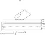
请参考图1,本发明的第一实施例提供一种显示器件10,所述显示器件10包括指纹检测模组10a、粘胶层12和显示模组13,所述显示模组13的其中一个表面为供用户进行操作的触摸面131,与触摸面131相对的另一个面上设置有粘胶层12,粘胶层12与指纹检测模组10a粘合以增强指纹检测模组10a与显示模组13的连接强度,所述指纹检测模组10a的尺寸与显示模组13的尺寸相当,所述指纹检测模组10a不仅可以进行指纹识别,而且可以进行全屏触控和压力检测。所述显示模组13可以是市场现有的一些包括显示层、盖板玻璃等基本结构的显示模组,但优选为包括OLED(有机发光二极管)或者TFT(薄膜晶体管)的显示模组。可以理解,所述粘胶层12可以省略,所述显示模组13靠近指纹检测模组10a的表面本身具有粘性,所述显示模组13直接与指纹检测模组10a粘接即可。(本发明中所提及的上下左右等方位词仅限于指定视图上的相对位置,而非绝对位置,可以理解,指定视图在平面内进行180°旋转后,位置词“下”即可以替换为位置词“上。”)Referring to FIG. 1, a first embodiment of the present invention provides adisplay device 10, thedisplay device 10 includes afingerprint detection module 10a, anadhesive layer 12 and adisplay module 13, one of thedisplay modules 13 The surface is atouch surface 131 for the user to operate, and the other surface opposite to thetouch surface 131 is provided with anadhesive layer 12. Theadhesive layer 12 is bonded to thefingerprint detection module 10a to strengthen thefingerprint detection module 10a and the display module. The connection strength of thegroup 13, the size of thefingerprint detection module 10a is equivalent to the size of thedisplay module 13, thefingerprint detection module 10a can not only perform fingerprint recognition, but also perform full-screen touch and pressure detection. Thedisplay module 13 may be some existing display modules in the market including a display layer, a cover glass and other basic structures, but preferably a display module including an OLED (Organic Light Emitting Diode) or a TFT (Thin Film Transistor). It can be understood that theadhesive layer 12 can be omitted, the surface of thedisplay module 13 close to thefingerprint detection module 10a is sticky, and thedisplay module 13 can be directly bonded to thefingerprint detection module 10a. (The azimuth words such as up, down, left, right, etc. mentioned in the present invention are limited to the relative position on the specified view, not the absolute position. It can be understood that after the specified view is rotated 180° in the plane, the position word "down" can be replaced by positional word "on.")

所述指纹检测模组10a包括检测模块11、升压电路层14、不导电基板15、电路板17、信号处理层18以及连接器19,所述检测模块11、不导电基板15和电路板17依次叠放形成叠层结构,其中检测模块11靠近显示模组13设置,不导电基板15位于检测模块11和电路板17之间,所述检测模块11与电路板17电性连接,所述电路板17还用于与外部电路电性连接。所述检测模块11可进行超声波信号和电信号之间的转换,所述信号处理层18、所述升压电路层14以及所述连接器19间隔设置在电路板17远离不导电基底15的表面上且均与电路板17电性连接,所述信号处理层18用于收集检测模块11传输过来的电信号并对电信号进行分析,所述升压电路层14用于对电路板17输出的电压信号进行升高,所述连接器19用于与外部电路电性连接。可以理解,所述信号处理层18可以是至少一个处理芯片,所述至少一个信号处理芯片可以执行指纹识别、触控识别和压力检测中的一种或多种功能;也可以是多个处理芯片间隔设置在电路板17上,每个处理芯片执行指纹识别、触控识别和压力检测中的一种或多种功能。可以理解,所述电路板17可以是印刷电路板、柔性电路板(FlexiblePrinted Circuit,简称FPC)或者其他具有导电结构的电路板,在本发明中优选为电路板17为柔性电路板,从而可以减小指纹检测模组10a的厚度。可以理解,所述连接器19优选为FPC连接器,使电路板17与外部电路的电性连接更稳固。还可以理解,所述不导电基板15优选为玻璃。Thefingerprint detection module 10a includes adetection module 11, abooster circuit layer 14, anon-conductive substrate 15, acircuit board 17, asignal processing layer 18 and aconnector 19. Thedetection module 11, thenon-conductive substrate 15 and thecircuit board 17 Stacked in sequence to form a laminated structure, wherein thedetection module 11 is arranged close to thedisplay module 13, thenon-conductive substrate 15 is located between thedetection module 11 and thecircuit board 17, thedetection module 11 is electrically connected to thecircuit board 17, and the circuit Theboard 17 is also used for electrical connection with external circuits. Thedetection module 11 can perform conversion between ultrasonic signals and electrical signals, and thesignal processing layer 18 , thebooster circuit layer 14 and theconnector 19 are arranged at intervals on the surface of thecircuit board 17 away from thenon-conductive substrate 15 . Thesignal processing layer 18 is used to collect the electrical signals transmitted from thedetection module 11 and analyze the electrical signals, and theboost circuit layer 14 is used for the output of thecircuit board 17. The voltage signal is boosted, and theconnector 19 is used for electrical connection with an external circuit. It can be understood that thesignal processing layer 18 can be at least one processing chip, and the at least one signal processing chip can perform one or more functions of fingerprint recognition, touch recognition and pressure detection; it can also be multiple processing chips The intervals are arranged on thecircuit board 17, and each processing chip performs one or more functions of fingerprint recognition, touch recognition and pressure detection. It can be understood that thecircuit board 17 can be a printed circuit board, a flexible printed circuit (FPC for short), or other circuit boards with a conductive structure. In the present invention, thecircuit board 17 is preferably a flexible circuit board, so as to reduce the The thickness of the smallfingerprint detection module 10a. It can be understood that theconnector 19 is preferably an FPC connector, so that the electrical connection between thecircuit board 17 and the external circuit is more stable. It can also be understood that thenon-conductive substrate 15 is preferably glass.

可以理解,优选的,在所述不导电基板15靠近指纹检测模组11的表面的边缘区域设置有多个引脚151,所述电路板17与该引脚151电性连接,所述检测模块11与引脚151电性连接。电路板17与引脚151通过焊接的方式实现电性连接,稳固性更好,电性连接的可靠性较佳。It can be understood that, preferably, a plurality ofpins 151 are provided in the edge area of thenon-conductive substrate 15 close to the surface of thefingerprint detection module 11, thecircuit board 17 is electrically connected to thepins 151, and thedetection module 11 is electrically connected to thepin 151 . Thecircuit board 17 and thepins 151 are electrically connected by welding, so that the stability is better and the reliability of the electrical connection is better.

请一并参考图1和图2,所述检测模块11包括上电极层111、压电层113和下电极层115,所述上电极层111和下电极层115分别设置在压电层113相对的两个表面上,其中上电极层111靠近显示模组13设置,所述上电极层111和下电极层115分别与电路板17电性连接。所述下电极层115包括多个呈阵列排布的电极块1153,多个电极块1153是设置在不导电基板15靠近检测模块11的表面上,所述多个电极块1153与多个引脚151对应地电性连接,从而实现电极块1153与电路板17的电性连接。所述多个电极块1153用于进行超声波信号的感应,由于手指的一个谷脊周期的宽度通常为300um,通过设置电极块1153的尺寸有利于保证识别的指纹的清晰度,从而确保指纹识别的精确性。优选的,所述电极块1153的面积小于或者等于70μm*70μm,进一步优选为小于或者等于60μm*60μm,更进一步优选40μm*40μm,电极块1153的尺寸在此范围内时,指纹识别效果最佳。可以理解,所述上电极层111也可以是包括多个阵列排布的电极块1153,且所述上电极层111的电极块1153的尺寸、位置与下电极层115的电极块1153的尺寸、位置一致。也可以理解,所述上电极层111和下电极层115之一为阵列排布的电极块1153即可实现指纹识别功能,当上电极层111包括多个阵列排布的电极块1153时,所述下电极层115可以为一整层电极。Please refer to FIG. 1 and FIG. 2 together. Thedetection module 11 includes anupper electrode layer 111 , apiezoelectric layer 113 and alower electrode layer 115 . Theupper electrode layer 111 and thelower electrode layer 115 are respectively disposed opposite to thepiezoelectric layer 113 . Theupper electrode layer 111 is disposed close to thedisplay module 13 on the two surfaces of theupper electrode layer 111 and thelower electrode layer 115 is electrically connected to thecircuit board 17 respectively. Thelower electrode layer 115 includes a plurality ofelectrode blocks 1153 arranged in an array, and the plurality ofelectrode blocks 1153 are arranged on the surface of thenon-conductive substrate 15 close to thedetection module 11 . The plurality ofelectrode blocks 1153 are connected with a plurality of pins. 151 are correspondingly electrically connected, so as to realize the electrical connection between theelectrode block 1153 and thecircuit board 17 . The plurality ofelectrode blocks 1153 are used to sense ultrasonic signals. Since the width of one valley ridge cycle of the finger is usually 300um, setting the size of the electrode blocks 1153 is conducive to ensuring the clarity of the identified fingerprint, thereby ensuring the accuracy of fingerprint identification. precision. Preferably, the area of theelectrode block 1153 is less than or equal to 70 μm*70 μm, more preferably less than or equal to 60 μm*60 μm, still more preferably 40 μm*40 μm, when the size of theelectrode block 1153 is within this range, the fingerprint recognition effect is the best . It can be understood that theupper electrode layer 111 may also include a plurality ofelectrode blocks 1153 arranged in an array, and the size and position of the electrode blocks 1153 of theupper electrode layer 111 are the same as the size and the position of the electrode blocks 1153 of thelower electrode layer 115. Same location. It can also be understood that if one of theupper electrode layer 111 and thelower electrode layer 115 is anelectrode block 1153 arranged in an array, the fingerprint recognition function can be realized. When theupper electrode layer 111 includes a plurality ofelectrode blocks 1153 arranged in an array, the Thelower electrode layer 115 can be a whole layer of electrodes.

压电层113为压电膜,优选的,压电层113为铁电聚合物薄膜,在一具体的实施方式中,所述铁电聚合物薄膜是通过采购现有的铁电聚合物薄膜成品,然后再通过粘附在基底上来进行极化而得到。通常,这种成品的铁电聚合物薄膜需要先被拉升具有一定应力然后再通过粘合在基底上再进行极化,此种方法形成的铁电聚合物薄膜厚度均在30μm以上,不适应现有电子器件轻薄的发展趋势,而且采用这种极化膜的检测模块,由于压电感测膜太厚,因此分辨率较低。上述实施方式中的铁电聚合物薄膜极化方法大都是直接在铁电聚合物薄膜的上下表面之间设置高压电场来进行,但是因为铁电聚合物薄膜本身厚度的不均,所以可能容易被高压电场所击穿,压电膜113的生产合格率十分低,不利于大规模生产,而且制得的压电膜113的压电效应较差,使用寿命较短。Thepiezoelectric layer 113 is a piezoelectric film. Preferably, thepiezoelectric layer 113 is a ferroelectric polymer film. In a specific embodiment, the ferroelectric polymer film is a finished product obtained by purchasing an existing ferroelectric polymer film. , and then polarized by adhering to the substrate. Usually, the finished ferroelectric polymer film needs to be pulled up to have a certain stress and then polarized by bonding on the substrate. The thickness of the ferroelectric polymer film formed by this method is all above 30 μm, which is not suitable for The development trend of existing electronic devices is light and thin, and the detection module using this polarized film has a low resolution because the piezoelectric sensing film is too thick. Most of the polarization methods of the ferroelectric polymer film in the above-mentioned embodiments are performed by directly setting a high-voltage electric field between the upper and lower surfaces of the ferroelectric polymer film. However, due to the uneven thickness of the ferroelectric polymer film itself, it may easily be When the high voltage electric field breaks down, the production qualification rate of thepiezoelectric film 113 is very low, which is not conducive to mass production, and thepiezoelectric film 113 produced has poor piezoelectric effect and short service life.

在另一具体的实施方式中,本发明的压电层113优选为原位极化形成的铁电聚合物薄膜,具体为所述压电层113是在带有电极块1153的不导电基板15的一面上原位形成压电膜113,所述压电膜113包括相对的第一表面和第二表面,所述第一表面即为靠近不导电基板15的一面,所述第二表面为靠近上电极层111的表面。极化时候,使该压电膜113的第一表面电势为零;在所述压电膜113的第二表面所在侧提供第一电场及第二电场,第一电场的电势高于第二电场的电势;在第一电场的作用下电离所述压电膜113第二表面所在的一侧的环境气体,该环境气体穿过第二电场而聚集在压电膜113的第二表面,使所述压电膜113内形成沿薄膜厚度方向的膜内电场,对所述压电膜113进行极化形成所述压电层113。可以理解,所述铁电聚合物薄膜通过化学气相沉积,涂覆、浸涂等湿化学方法形成在下电极层115表面,因此可以形成厚度很薄且均匀的铁电聚合物薄膜,厚度可以小于30μm,优选的,厚度可以维持在9μm以下,从而减小信号的传输损耗,形成工艺简单,而且,采用这种原位形成的极化膜的检测模块11,分辨率大大提高。所述压电层113的厚度可进一步为小于9μm,再进一步地,其厚度可为1.5-7.4μm、1.9-7.2μm、2.2-8.6μm、2.8-8.4μm或者3.6-6.6μm,更进一步地,可以具体是1.8μm、2.4μm、2.6μm、3.7μm、3.9μm、4.2μm、4.6μm、5.6μm、5.8μm、6.7μm、8.6μm、8.7μm。In another specific embodiment, thepiezoelectric layer 113 of the present invention is preferably a ferroelectric polymer film formed by in-situ polarization. Specifically, thepiezoelectric layer 113 is formed on anon-conductive substrate 15 with electrode blocks 1153 . Apiezoelectric film 113 is formed in situ on one side of the substrate. Thepiezoelectric film 113 includes an opposite first surface and a second surface, the first surface is the side close to thenon-conductive substrate 15, and the second surface is close to the the surface of theupper electrode layer 111 . During polarization, the potential of the first surface of thepiezoelectric film 113 is set to zero; a first electric field and a second electric field are provided on the side where the second surface of thepiezoelectric film 113 is located, and the potential of the first electric field is higher than that of the second electric field Under the action of the first electric field, the ambient gas on the side where the second surface of thepiezoelectric film 113 is located is ionized, and the ambient gas passes through the second electric field and gathers on the second surface of thepiezoelectric film 113, so that all Thepiezoelectric film 113 forms an electric field in the film along the thickness direction of the film, and thepiezoelectric film 113 is polarized to form thepiezoelectric layer 113 . It can be understood that the ferroelectric polymer film is formed on the surface of thelower electrode layer 115 by wet chemical methods such as chemical vapor deposition, coating, dip coating, etc., so a thin and uniform ferroelectric polymer film can be formed, and the thickness can be less than 30 μm , preferably, the thickness can be maintained below 9 μm, thereby reducing the transmission loss of the signal, the formation process is simple, and the resolution of thedetection module 11 using the polarized film formed in situ is greatly improved. The thickness of thepiezoelectric layer 113 may be further less than 9 μm, and further, the thickness may be 1.5-7.4 μm, 1.9-7.2 μm, 2.2-8.6 μm, 2.8-8.4 μm or 3.6-6.6 μm, and furthermore , can be specifically 1.8 μm, 2.4 μm, 2.6 μm, 3.7 μm, 3.9 μm, 4.2 μm, 4.6 μm, 5.6 μm, 5.8 μm, 6.7 μm, 8.6 μm, 8.7 μm.

再者,本发明相较于直接在压电层113的上下表面设置电极的极化方法,上述虚拟极化方法不会使压电层113直接承受所施加的高压电场,能避免压电层113被击穿。具体的,上述极化可采用离子体极化(具体可参见申请号为201710108374.9的中国专利申请)或X射线极化(具体可参见申请号为201611222575.3的中国专利申请)的方式形成所述压电层,所形成的压电层113能够做到很薄,而且,本发明的压电层113的压电效应较好以及使用寿命长,能够很好的适用在检测模块11中,利于实现检测模块11较好的识别效果。在此具体实施方式中,进行了原位极化的所述压电层113的压电常数d33的范围为20-35pC/N,进一步优选为25~29pC/N。Furthermore, compared with the polarization method of directly disposing electrodes on the upper and lower surfaces of thepiezoelectric layer 113 in the present invention, the above-mentioned virtual polarization method does not allow thepiezoelectric layer 113 to directly withstand the applied high-voltage electric field, and can avoid thepiezoelectric layer 113 was penetrated. Specifically, the above-mentioned polarization can be formed by ion polarization (for details, please refer to the Chinese patent application with application number 201710108374.9) or X-ray polarization (for details, please refer to the Chinese patent application with application number 201611222575.3). The formedpiezoelectric layer 113 can be made very thin, and the piezoelectric effect of thepiezoelectric layer 113 of the present invention is good and the service life is long, and can be well applied in thedetection module 11, which is conducive to the realization of the detection module. 11 Better recognition effect. In this specific embodiment, the piezoelectric constant d33 of thepiezoelectric layer 113 subjected to in-situ polarization is in the range of 20-35 pC/N, more preferably 25-29 pC/N.

可以理解,所述压电层113的材料为铁电聚合物材料,具体可选用但不限于:聚偏氟乙烯,聚氯乙烯,聚-γ-甲基-L-谷氨酸酯,聚碳酸酯、聚偏氟乙烯、聚偏二氟乙烯PVDF、聚偏二氟乙烯三氟乙烯PVDF-TrFE、聚甲基丙烯酸甲酯PMMA、聚四氟乙烯TEFLON等共聚物中的一种或者几种的组合。It can be understood that the material of thepiezoelectric layer 113 is a ferroelectric polymer material, which can be specifically selected but not limited to: polyvinylidene fluoride, polyvinyl chloride, poly-γ-methyl-L-glutamate, polycarbonate Ester, polyvinylidene fluoride, polyvinylidene fluoride PVDF, polyvinylidene fluoride trifluoroethylene PVDF-TrFE, polymethyl methacrylate PMMA, polytetrafluoroethylene TEFLON and other copolymers one or more combination.

在本发明的一些实施例中,所述压电层113的材料选用聚偏氟乙烯的共聚物为聚偏氟乙烯-三氟乙烯共聚物,具体的为聚偏二氟乙烯三氟乙烯PVDF-TrFE,为了获得压电效应较好的压电层,所述聚偏二氟乙烯与三氟乙烯的质量比的范围是(60-95):(5-30),优选地,其质量比的范围是(75-86):(15-25),进一步优选地,其质量比为80:20或75:25或70:30,所述聚偏二氟乙烯和三氟乙烯共聚物较单独选用聚偏二氟乙烯可降低成本,且其还具有较好的压电效应。In some embodiments of the present invention, the material of thepiezoelectric layer 113 is a polyvinylidene fluoride-trifluoroethylene copolymer, specifically polyvinylidene fluoride-trifluoroethylene PVDF- TrFE, in order to obtain a piezoelectric layer with better piezoelectric effect, the range of the mass ratio of the polyvinylidene fluoride to trifluoroethylene is (60-95): (5-30), preferably, the mass ratio of The range is (75-86): (15-25), further preferably, its mass ratio is 80:20 or 75:25 or 70:30, and the polyvinylidene fluoride and trifluoroethylene copolymer are selected separately Polyvinylidene fluoride can reduce costs, and it also has a better piezoelectric effect.

所述铁电聚合物薄膜极化后所得的压电膜113内既有α相晶粒也有β相晶粒以及非晶态物质,β相的含量与压电膜113的压电效应相对应,当β相晶粒占总晶粒的含量为60-70%时,极化膜即具有较好的压电效应,β相的含量越高极化膜的压电效应越好。然而过度极化会产生多余的不必要的电荷等,这些多余电荷容易与聚合物表面上的其他电荷重新结合,从而影响所得压电膜的性能。在本实施例中,所述高分子压电膜113的β相晶粒与总晶粒质量比为60~70%。Thepiezoelectric film 113 obtained after the polarization of the ferroelectric polymer film has both α-phase crystal grains, β-phase crystal grains and amorphous substances, and the content of the β-phase corresponds to the piezoelectric effect of thepiezoelectric film 113 . When the content of β-phase grains in the total grains is 60-70%, the polarized film has a better piezoelectric effect, and the higher the content of β-phase, the better the piezoelectric effect of the polarized film. Excessive polarization, however, can generate excess unwanted charges, etc., which easily recombine with other charges on the polymer surface, thereby affecting the performance of the resulting piezoelectric film. In this embodiment, the mass ratio of the β-phase crystal grains to the total crystal grains of thepolymer piezoelectric film 113 is 60-70%.

请参考图3,可以理解,通常显示模组13中都会包含一个驱动芯片,其可以驱动显示模组13工作。作为一种变形,电路板17可以与显示模组13电性连接,可以将显示模组13的驱动芯片的功能集成到信号处理层18上,从而信号处理层18既能进行电信号的收集和分析以实现指纹识别、触控识别以及压力检测功能,又能驱动显示模组13工作,不仅降低了整个显示器件10的厚度,节约了生产成本,而且提高了电子元器件的集成度,更加符合精密制造的需求。Please refer to FIG. 3 , it can be understood that thedisplay module 13 usually includes a driver chip, which can drive thedisplay module 13 to work. As a variant, thecircuit board 17 can be electrically connected to thedisplay module 13, and the function of the driver chip of thedisplay module 13 can be integrated into thesignal processing layer 18, so that thesignal processing layer 18 can both collect and process electrical signals. The analysis can realize the functions of fingerprint recognition, touch recognition and pressure detection, and can also drive thedisplay module 13 to work, which not only reduces the thickness of theentire display device 10, saves the production cost, but also improves the integration of electronic components, which is more in line with the Precision manufacturing needs.

本实施例的指纹检测模组10a的尺寸与显示模组13的尺寸相当,因此其可以进行全屏超声波指纹识别,在显示模组13的任意位置处触摸均可以进行指纹识别。指纹检测模组10a的一个工作周期包括发射阶段和接收阶段两部分。发射阶段,外部电路依次通过电路板17同时分别给予上电极层111和下电极层115电压信号,当给予上电极层111的电压信号高于给予下电极层115的电压信号时,无需再通过升压电路层14对给予上电极层111的电压信号进行升高;当给予上电极层111和下电极层115相同的电压信号时,升压电路层13对电路板17传输给上电极层111的电压信号进行升高;当上电极层111的电势高于下电极层115的电势时,压电层113的两侧形成一电势差,进而产生机械振动并发出超声波,此时外部电路已停止给予上电极层111和下电极层115电压信号;接收阶段,压电层113发出的超声波接触到手指后反射,由于指纹谷处与指纹脊处相比存在更多的空气,因此手指的指纹谷和指纹脊处反射的信号强度不同,通常指纹谷所反射的超声波的能量会比指纹脊所反射的超声波能量大,即指纹谷所反射的信号强度要强于指纹脊所反射的信号强度,压电层113接收到指纹谷和指纹脊所反射回来的不同超声波信号从而产生不同的电信号,通过设置电极块1153的尺寸,使手指的一个谷脊周期对应于多个电极块1153,因此,分别对应于指纹谷和指纹脊的电极块1153由于静电耦合的作用产生不同数量的感应电荷,信号处理层18通过检测感应电荷的数量的差异来实现指纹识别,最后将检测结果通过电路板17传递给外部电路。The size of thefingerprint detection module 10a in this embodiment is equivalent to the size of thedisplay module 13, so it can perform full-screen ultrasonic fingerprint recognition, and fingerprint recognition can be performed by touching any position of thedisplay module 13. A working cycle of thefingerprint detection module 10a includes two parts: a transmitting phase and a receiving phase. In the emission stage, the external circuit sequentially gives voltage signals to theupper electrode layer 111 and thelower electrode layer 115 through thecircuit board 17 respectively. Thebooster circuit layer 14 boosts the voltage signal given to theupper electrode layer 111 ; when the same voltage signal is given to theupper electrode layer 111 and thelower electrode layer 115 , thebooster circuit layer 13 transmits the voltage signal from thecircuit board 17 to theupper electrode layer 111 . The voltage signal is increased; when the potential of theupper electrode layer 111 is higher than the potential of thelower electrode layer 115, a potential difference is formed on both sides of thepiezoelectric layer 113, which in turn generates mechanical vibration and sends out ultrasonic waves. At this time, the external circuit has stopped giving the upper The voltage signal of theelectrode layer 111 and thelower electrode layer 115; in the receiving stage, the ultrasonic wave emitted by thepiezoelectric layer 113 is reflected after touching the finger. Since there is more air at the fingerprint valley than at the fingerprint ridge, the fingerprint valley of the finger and the fingerprint The signal strengths reflected at the ridges are different. Usually, the energy of the ultrasonic waves reflected by the fingerprint valleys is larger than that of the fingerprint ridges, that is, the signal strength reflected by the fingerprint valleys is stronger than the signal strength reflected by the fingerprint ridges. Thepiezoelectric layer 113 Different ultrasonic signals reflected by fingerprint valleys and fingerprint ridges are received to generate different electrical signals. By setting the size of theelectrode block 1153, one valley and ridge cycle of the finger corresponds to a plurality ofelectrode blocks 1153, thus corresponding to fingerprints respectively. The electrode blocks 1153 of the valley and the fingerprint ridge generate different amounts of induced charges due to electrostatic coupling. Thesignal processing layer 18 realizes fingerprint recognition by detecting the difference in the amount of induced charges, and finally transmits the detection results to the external circuit through thecircuit board 17 .

可以理解,为了方便检测压电层113接收显示模组13反射回来的超声波信号,需要设置一定的时间差来避免向显示模组13传播的超声波信号和显示模组13反射回来的超声波信号混合,从而确保检测的精准度。例如,外部电路按照一定的时间规律给压电层113提供电势差以发出超声波信号。It can be understood that, in order to facilitate the detection of thepiezoelectric layer 113 to receive the ultrasonic signal reflected from thedisplay module 13, a certain time difference needs to be set to avoid mixing the ultrasonic signal transmitted to thedisplay module 13 and the ultrasonic signal reflected from thedisplay module 13, thereby Ensure detection accuracy. For example, an external circuit provides a potential difference to thepiezoelectric layer 113 according to a certain time law to emit ultrasonic signals.

本发明实施例的指纹检测模组10a还可以进行触控识别。所述信号处理层18集成有触控芯片的功能,在显示模组13的表面未发生触摸的情况下,压电层113所发出的超声波信号会被显示模组13的表面反射,压电层113可以检测到反射回来的超声波信号并产生电信号,而电极块1153由于静电耦合的作用会产生一定数量的感应电荷;如图1所示,在显示模组13的表面发生触摸的情况时,由于触摸物(例如用户的手指,图1中仅示出用户手指的部分指纹,详见图中的锯齿状线条)与显示模组13的表面之间的接触可以使部分超声波信号透过显示模组13进入该触摸物中,因此压电层113接收到的触摸位置显示模组13反射回来的超声波信号会发生变化,从而压电层113在触摸位置处产生的电信号会发生变化,从而对应位置处的电极块1153产生的感应电荷的数量也会发生变化,而未被触摸的位置处显示模组13反射回来的超声波信号未发生变化,从而未被触摸位置处对应的电极块1153产生的感应电荷的数量未发生变化,因此,通过信号处理层18检测被触摸位置处与未被触摸位置处的感应电荷的数量是否发生变化来判断出触摸位置,即实现超声波触控。Thefingerprint detection module 10a of the embodiment of the present invention can also perform touch recognition. Thesignal processing layer 18 integrates the function of a touch chip. When the surface of thedisplay module 13 is not touched, the ultrasonic signal emitted by thepiezoelectric layer 113 will be reflected by the surface of thedisplay module 13. 113 can detect the reflected ultrasonic signal and generate an electrical signal, and theelectrode block 1153 will generate a certain amount of induced charges due to electrostatic coupling; as shown in FIG. 1, when the surface of thedisplay module 13 is touched, Due to the contact between the touch object (such as the user's finger, only part of the fingerprint of the user's finger is shown in FIG. 1, see the zigzag lines in the figure for details) and the surface of thedisplay module 13, part of the ultrasonic signal can be transmitted through the display module. Thegroup 13 enters the touch object, so the ultrasonic signal reflected by the touchposition display module 13 received by thepiezoelectric layer 113 will change, so that the electrical signal generated by thepiezoelectric layer 113 at the touch position will change, corresponding to The amount of induced charges generated by theelectrode block 1153 at the position will also change, while the ultrasonic signal reflected by thedisplay module 13 at the untouched position does not change, so the correspondingelectrode block 1153 at the untouched position generates no change. The quantity of the induced charges does not change, therefore, the touch position is determined by detecting whether the quantity of the induced charges at the touched position and the untouched position changes by thesignal processing layer 18 , that is, ultrasonic touch is realized.

本发明实施例的指纹检测模组10a还可以进行压力感测,下面结合图4来进行压力感测原理的说明。如图4所示,当手指施加压力时,压电层113会发生形变,当施加的压力大小不一样时,压电层113的形变程度不一样,从而电极块1153产生的感应电荷的数量就不一样,压电层113的形变程度越大时,电极块1153产生的感应电荷的数量就更多;压电层113的形变程度越小时,电极块1153产生的感应电荷的数量就更少;因此,信号处理层18通过检测电极块1153产生的感应电荷的数量大小来确定压力大小,即实现压力检测。可以理解,所述信号处理层18可以是多个芯片的集成,从而实现不同信号的检测与分析进而使指纹检测模组10a可以实现指纹识别,压力感测以及触控等功能之一种或多种。Thefingerprint detection module 10a of the embodiment of the present invention can also perform pressure sensing. The following describes the pressure sensing principle with reference to FIG. 4 . As shown in FIG. 4 , when the finger applies pressure, thepiezoelectric layer 113 will deform. When the applied pressure is different, the deformation degree of thepiezoelectric layer 113 is different, so that the amount of induced charges generated by theelectrode block 1153 is Differently, the greater the deformation degree of thepiezoelectric layer 113, the greater the amount of induced charges generated by theelectrode block 1153; the smaller the deformation degree of thepiezoelectric layer 113, the smaller the amount of induced charges generated by theelectrode block 1153; Therefore, thesignal processing layer 18 determines the magnitude of the pressure by detecting the quantity of the induced charges generated by theelectrode block 1153, that is, the pressure detection is realized. It can be understood that thesignal processing layer 18 can be the integration of multiple chips, so as to realize the detection and analysis of different signals, so that thefingerprint detection module 10a can realize one or more functions of fingerprint recognition, pressure sensing and touch control. kind.

本发明的第一实施例还提供一种电子设备,其采用如上所述的指纹检测模组10a或显示器件11。所述电子设备包括但不限于手机、电脑、平板电脑、考勤机等刷指纹的设备。The first embodiment of the present invention also provides an electronic device, which adopts thefingerprint detection module 10a or thedisplay device 11 as described above. The electronic devices include but are not limited to devices for swiping fingerprints such as mobile phones, computers, tablet computers, and attendance machines.

第二实施例Second Embodiment

请参考图5,本发明的第二实施例还提供另一种结构的显示器件20,所述显示器件20包括呈层叠结构的盖板21、第一压电模组20a、第二压电模组21a、显示模组22、粘胶层23、不导电基板25及电路板27。所述盖板21的其中一个表面为供用户进行操作的触摸面2111,与触摸面2111相对的另一个面上设置有第一压电模组20a。所述第一压电模组20a和第二压电模组21a设置在显示模组22相背的两个表面上,所述粘胶层23设置在显示模组22远离盖板21的表面上且位于第二压电模组21a和显示模组22之间。所述不导电基板25设置在第二压电模组21a远离显示模组22的表面上。所述电路板27设置在不导电基板25远离显示模组22的表面上。可以理解,所述第一压电模组20a和第二压电模组21a两者的位置可以进行对换。所述第一压电模组20a和第二压电模组21a均与电路板27电性连接。所述第一压电模组20a、第二压电模组21a、显示模组22以及盖板21的尺寸相当。可以理解,所述粘胶层23可以省略,所述显示模组22靠近第二压电模组21a的表面本身有粘性,所述显示模组22直接与第二压电模组21a粘接即可。(本实施例中所提及的上下左右等方位词仅限于指定视图上的相对位置,而非绝对位置,例如,可以理解,指定视图在平面内进行180°旋转后,位置词“下”即可以替换为位置词“上”。)Please refer to FIG. 5 , the second embodiment of the present invention further provides adisplay device 20 with another structure, thedisplay device 20 includes acover plate 21 in a stacked structure, a firstpiezoelectric module 20a, a second piezoelectric module Thegroup 21 a , thedisplay module 22 , theadhesive layer 23 , thenon-conductive substrate 25 and thecircuit board 27 . One surface of thecover plate 21 is atouch surface 2111 for the user to operate, and the other surface opposite to thetouch surface 2111 is provided with a firstpiezoelectric module 20a. The firstpiezoelectric module 20a and the secondpiezoelectric module 21a are disposed on two opposite surfaces of thedisplay module 22, and theadhesive layer 23 is disposed on the surface of thedisplay module 22 away from thecover plate 21 and is located between the secondpiezoelectric module 21 a and thedisplay module 22 . Thenon-conductive substrate 25 is disposed on the surface of the secondpiezoelectric module 21a away from thedisplay module 22 . Thecircuit board 27 is disposed on the surface of thenon-conductive substrate 25 away from thedisplay module 22 . It can be understood that the positions of the firstpiezoelectric module 20a and the secondpiezoelectric module 21a can be exchanged. The firstpiezoelectric module 20a and the secondpiezoelectric module 21a are both electrically connected to thecircuit board 27 . The firstpiezoelectric module 20a, the secondpiezoelectric module 21a, thedisplay module 22 and thecover plate 21 have the same size. It can be understood that theadhesive layer 23 can be omitted, the surface of thedisplay module 22 close to the secondpiezoelectric module 21a is sticky, and thedisplay module 22 is directly bonded to the secondpiezoelectric module 21a, that is, Can. (The directional words such as up, down, left, right, etc. mentioned in this embodiment are only limited to the relative position on the specified view, not the absolute position. For example, it can be understood that after the specified view is rotated 180° in the plane, the position word "down" is Can be replaced with the positional word "on".)

可以理解,所述盖板21为透明材质,且盖板16的材质的声阻抗和显示模块17的声阻抗相近,优选为玻璃。所述电路板27可以是印刷电路板、柔性电路板或者其他具有导电结构的电路板,在本发明中优选为电路板27为柔性电路板。还可以理解,所述不导电基板25优选为玻璃。It can be understood that thecover plate 21 is made of a transparent material, and the acoustic impedance of the material of the cover plate 16 is similar to that of thedisplay module 17 , preferably glass. Thecircuit board 27 may be a printed circuit board, a flexible circuit board, or other circuit boards with a conductive structure. In the present invention, thecircuit board 27 is preferably a flexible circuit board. It can also be understood that thenon-conductive substrate 25 is preferably glass.

可以理解,所述显示器件20进一步包括信号处理层28、升压电路层24和连接器29,所述信号处理层28、升压电路层24和连接器29间隔设置在电路板27远离不导电基板25的表面上且与电路板27电性连接。It can be understood that thedisplay device 20 further includes asignal processing layer 28, abooster circuit layer 24 and aconnector 29, and thesignal processing layer 28, thebooster circuit layer 24 and theconnector 29 are arranged at intervals on thecircuit board 27 away from the non-conductive The surface of thesubstrate 25 is electrically connected with thecircuit board 27 .

请一并参考图5和图6,所述第一压电模组20a包括第一电极层211、第一压电层213和第二电极层215,所述第一电极层211和第二电极层215设置在第一压电层213两个相背的表面上,且所述第一电极层211远离显示模组22设置,所述第一电极层211和第二电极层215均与电路板27电性连接。第一电极层211和第二电极层215两者中至少有其一包括多个阵列排布的第一导电块2153,当第一电极层211和第二电极层215两者均包括多个阵列排布的第一导电块2153时,第一电极层211的第一导电块2153和第二电极层215的第一导电块2153尺寸一致、位置一一对应。由于第一压电模组20a设置在显示模组22靠近盖板21的一侧,故而第一电极层211、第一压电层213和第二电极层215均由透明材质制成。可以理解,所述第一电极层211和第二电极层215可以是氧化铟锡、氧化铟镓锌等透明导电金属氧化物,所述第一压电层213的材料可以是透明铁电压电陶瓷或者透明聚偏氟乙烯压电材料等。Please refer to FIG. 5 and FIG. 6 together, the firstpiezoelectric module 20a includes afirst electrode layer 211 , a firstpiezoelectric layer 213 and asecond electrode layer 215 . Thefirst electrode layer 211 and the second electrode Thelayer 215 is disposed on two opposite surfaces of the firstpiezoelectric layer 213, and thefirst electrode layer 211 is disposed away from thedisplay module 22. Thefirst electrode layer 211 and thesecond electrode layer 215 are both connected to the circuit board. 27 Electrical connection. At least one of thefirst electrode layer 211 and thesecond electrode layer 215 includes a plurality of firstconductive blocks 2153 arranged in an array, and when both thefirst electrode layer 211 and thesecond electrode layer 215 include a plurality of arrays When the firstconductive blocks 2153 are arranged, the firstconductive blocks 2153 of thefirst electrode layer 211 and the firstconductive blocks 2153 of thesecond electrode layer 215 have the same size and corresponding positions. Since the firstpiezoelectric module 20a is disposed on the side of thedisplay module 22 close to thecover plate 21, thefirst electrode layer 211, the firstpiezoelectric layer 213 and thesecond electrode layer 215 are all made of transparent materials. It can be understood that thefirst electrode layer 211 and thesecond electrode layer 215 may be transparent conductive metal oxides such as indium tin oxide, indium gallium zinc oxide, etc., and the material of the firstpiezoelectric layer 213 may be transparent ferroelectric ceramics Or transparent polyvinylidene fluoride piezoelectric material, etc.

请一并参考图5和图7,所述第二压电模组21a包括第三电极层221、第二压电层223和第四电极层225,所述第三电极层221和第四电极层225设置在第二压电层223两个相背的表面上,且第三电极层221靠近显示模组22设置,所述第三电极层221和第四电极层225均与电路板27电性连接。第三电极层221和第四电极层225两者中至少有其一包括多个阵列排布的第二导电块2253,当第三电极层221和第四电极层225两者均包括多个阵列排布的第二导电块2253时,第三电极层221的第二导电块2253和第四电极层225的第二导电块2253尺寸一致、位置一一对应。可以理解,在本实施例中,第四电极层225的第二导电块2253是形成在不导电基板25靠近显示模组22的表面上的。Please refer to FIG. 5 and FIG. 7 together, the secondpiezoelectric module 21 a includes a third electrode layer 221 , a second piezoelectric layer 223 and afourth electrode layer 225 . The third electrode layer 221 and the fourth electrode Thelayer 225 is disposed on two opposite surfaces of the second piezoelectric layer 223, and the third electrode layer 221 is disposed close to thedisplay module 22. Both the third electrode layer 221 and thefourth electrode layer 225 are electrically connected to thecircuit board 27. sexual connection. At least one of the third electrode layer 221 and thefourth electrode layer 225 includes a plurality of second conductive blocks 2253 arranged in an array, and when both the third electrode layer 221 and thefourth electrode layer 225 include a plurality of arrays When the second conductive blocks 2253 are arranged, the second conductive blocks 2253 of the third electrode layer 221 and the second conductive blocks 2253 of thefourth electrode layer 225 have the same size and correspond one-to-one positions. It can be understood that, in this embodiment, the second conductive blocks 2253 of thefourth electrode layer 225 are formed on the surface of thenon-conductive substrate 25 close to thedisplay module 22 .

可以理解,所述第一导电块2153和第二导电块2253与第一实施例中的导电块1153是一样的,故在此不再赘述。It can be understood that the firstconductive block 2153 and the second conductive block 2253 are the same as theconductive block 1153 in the first embodiment, so they are not repeated here.

可以理解,所述第一压电层213和第二压电层223均为压电膜,优选的,第一压电层213和第二压电层223均为原位极化的铁电聚合物薄膜。在本实施例中,第一压电层213是在第二电极层215上进行原位极化得到的,第二压电层223是带有电极块2253的不导电基板25上原位形成的,在关于原位极化的内容与第一实施例中一致,故在此不再赘述。It can be understood that the firstpiezoelectric layer 213 and the second piezoelectric layer 223 are both piezoelectric films. Preferably, the firstpiezoelectric layer 213 and the second piezoelectric layer 223 are both in-situ polarized ferroelectric polymers material film. In this embodiment, the firstpiezoelectric layer 213 is obtained by in-situ polarization on thesecond electrode layer 215, and the second piezoelectric layer 223 is formed in-situ on thenon-conductive substrate 25 with electrode blocks 2253. , the content about the in-situ polarization is the same as that in the first embodiment, so it is not repeated here.

可以理解,在不导电基板25靠近检测模块21的表面的边缘区域设置有多个引脚251,所述第四电极层215的第二导电块2253分别与引脚251电性连接,所述电路板27与引脚251电性连接。通过设置引脚251来实现第二电极块2253与电路板27的电性连接,既可以减少加工难度,不用将第二电极块2253一一个单独地与电路板电性连接,而且引脚251可以做成块状的,在电路板27与引脚251连接更稳固,可靠性更高,而且工艺简单。It can be understood that a plurality ofpins 251 are provided in the edge area of thenon-conductive substrate 25 close to the surface of thedetection module 21 , and the second conductive blocks 2253 of thefourth electrode layer 215 are electrically connected to thepins 251 respectively. The circuit Theboard 27 is electrically connected to thepin 251 . The electrical connection between the second electrode block 2253 and thecircuit board 27 is realized by arranging thepins 251, which can reduce the difficulty of processing. It can be made into a block shape, the connection between thecircuit board 27 and thepin 251 is more stable, the reliability is higher, and the process is simple.

本实施例的显示器件20可以实现不同的压电模组执行不同的功能,第一压电模组20a和第二压电模组21a均可以执行压力检测、触控识别和指纹检测功能中的一种或多种。本实施例的信号处理层可以控制第一压电模组20a和第二压电模组21a执行不同的功能,例如,第一压电模组20a执行压力检测功能,第二压电模组21a执行触控识别和指纹检测功能;或第一压电模组20a执行压力检测、触控识别,第二压电模组21a执行指纹识别。作为优选的,第一压电模组20a执行压力检测功能,第二压电模组21a执行触控和指纹识别功能,因为其靠近盖板21设置,对压力的感应最为灵敏,执行压力检测时更加精确。Thedisplay device 20 of this embodiment can implement different piezoelectric modules to perform different functions, and both the firstpiezoelectric module 20a and the secondpiezoelectric module 21a can perform pressure detection, touch recognition and fingerprint detection functions. one or more. The signal processing layer of this embodiment can control the firstpiezoelectric module 20a and the secondpiezoelectric module 21a to perform different functions. For example, the firstpiezoelectric module 20a performs a pressure detection function, and the secondpiezoelectric module 21a performs a pressure detection function. Perform touch recognition and fingerprint detection functions; or the firstpiezoelectric module 20a performs pressure detection and touch recognition, and the secondpiezoelectric module 21a performs fingerprint recognition. Preferably, the firstpiezoelectric module 20a performs the pressure detection function, and the secondpiezoelectric module 21a performs the touch and fingerprint recognition functions, because it is located close to thecover plate 21, and is most sensitive to pressure sensing. more precise.

本实施例中的指纹识别、压力检测和触控识别过程的原理与第一实施例一致,故在此不再赘述。The principles of the fingerprint identification, pressure detection and touch identification processes in this embodiment are the same as those in the first embodiment, so they will not be repeated here.

本发明的第二实施例还提供一种电子设备,其采用如上所述的显示器件20。所述电子设备包括但不限于手机、电脑、平板电脑、考勤机等刷指纹的设备。The second embodiment of the present invention also provides an electronic device employing thedisplay device 20 as described above. The electronic devices include but are not limited to devices for swiping fingerprints such as mobile phones, computers, tablet computers, and attendance machines.

与现有技术相比,本发明的其用于设置在显示模组用于显示的一侧的相对侧,其实现指纹识别,压力感测和触控识别中的至少一种功能,从靠近显示模组朝远离显示模组的方向,所述指纹检测模组包括依次叠层设置的上电极层、压电层、下电极层、不导电基板和电路板,所述电路板分别与上电极层、下电极层电性连接,所述指纹检测模组的尺寸与显示模组的尺寸相当。本发明的指纹检测模组不仅具有结构简单,可靠性高的优点,更加符合电子设备轻薄化、集成度高的趋势,而且可以进行全屏指纹识别、触控识别和压力检测,功能多样。Compared with the prior art, in the present invention, it is arranged on the opposite side of the display module used for display, and realizes at least one function of fingerprint recognition, pressure sensing and touch recognition. The module faces the direction away from the display module, and the fingerprint detection module includes an upper electrode layer, a piezoelectric layer, a lower electrode layer, a non-conductive substrate and a circuit board that are stacked in sequence, and the circuit board is respectively connected to the upper electrode layer. , the lower electrode layer is electrically connected, and the size of the fingerprint detection module is equivalent to the size of the display module. The fingerprint detection module of the present invention not only has the advantages of simple structure and high reliability, but also conforms to the trend of thin and light electronic equipment and high integration, and can perform full-screen fingerprint recognition, touch recognition and pressure detection, and has various functions.

另外的,本发明的所述压电层为原位极化的铁电聚合物薄膜,具有压电效应好、分辨率高的优点。In addition, the piezoelectric layer of the present invention is an in-situ polarized ferroelectric polymer film, which has the advantages of good piezoelectric effect and high resolution.

与现有技术相比,本发明的显示器件包括显示模组和如上所述的指纹检测模组,所述显示模组的其中一个表面为供用户进行操作的触摸面,与触摸面相对的另一个面上设置所述指纹检测模组,所述显示模组的尺寸与指纹检测模组的尺寸一致。本发明的显示器件不仅具有结构简单,可靠性高的优点,更加符合电子设备轻薄化、集成度高的趋势,而且可以进行全屏指纹识别、触控识别和压力检测,功能多样。Compared with the prior art, the display device of the present invention includes a display module and the above-mentioned fingerprint detection module, wherein one surface of the display module is a touch surface for the user to operate, and the other surface opposite to the touch surface. The fingerprint detection module is arranged on one surface, and the size of the display module is consistent with the size of the fingerprint detection module. The display device of the invention not only has the advantages of simple structure and high reliability, but also conforms to the trend of thin and light electronic equipment and high integration, and can perform full-screen fingerprint recognition, touch recognition and pressure detection, and has various functions.

与现有技术相比,本发明的电子设备,其包括如上所述的指纹检测模组。本发明的电子设备具有集成度高,可靠性高,更轻薄的优点,而且可以进行全屏指纹识别、触控识别和压力检测,功能多样。Compared with the prior art, the electronic device of the present invention includes the fingerprint detection module as described above. The electronic device of the present invention has the advantages of high integration, high reliability, and is thinner and lighter, and can perform full-screen fingerprint recognition, touch recognition and pressure detection, and has various functions.

以上所述仅为本发明的较佳实施例而已,并不用以限制本发明,凡在本发明的原则之内所作的任何修改,等同替换和改进等均应包含本发明的保护范围之内。The above descriptions are only preferred embodiments of the present invention, and are not intended to limit the present invention. Any modifications, equivalent replacements and improvements made within the principles of the present invention should be included within the protection scope of the present invention.

Claims (9)

Translated fromChinese
1.一种指纹检测模组,其用于设置在显示模组用于显示的一侧的相对侧,其实现指纹识别,压力感测和触控识别中的至少一种功能,其特征在于:从靠近显示模组朝远离显示模组的方向,所述指纹检测模组包括依次叠层设置的上电极层、压电层、下电极层、不导电基板和电路板,所述电路板分别与上电极层、下电极层电性连接,所述指纹检测模组的尺寸与显示模组的尺寸相当;1. a fingerprint detection module, it is used for being arranged on the opposite side of one side that the display module is used for displaying, it realizes at least one function in fingerprint identification, pressure sensing and touch identification, it is characterized in that: From the direction close to the display module to the direction away from the display module, the fingerprint detection module includes an upper electrode layer, a piezoelectric layer, a lower electrode layer, a non-conductive substrate and a circuit board that are stacked in sequence, and the circuit boards are respectively connected to The upper electrode layer and the lower electrode layer are electrically connected, and the size of the fingerprint detection module is equivalent to that of the display module;所述指纹检测模组进行指纹识别的工作周期包括发射阶段和接收阶段,发射阶段对所述上电极层和所述下电极层同时施加电压信号并调节所述上电极层的电势高于所述下电极层的电势,以使所述压电层两侧形成一电势差并发出超声波,接收阶段所述压电层接收反射回来的不同能量损耗的超声波并产生不同的电信号;The working cycle of the fingerprint detection module for fingerprint identification includes an emission stage and a reception stage. In the emission stage, a voltage signal is simultaneously applied to the upper electrode layer and the lower electrode layer, and the potential of the upper electrode layer is adjusted to be higher than that of the upper electrode layer. The potential of the lower electrode layer, so that a potential difference is formed on both sides of the piezoelectric layer and ultrasonic waves are emitted, and the piezoelectric layer receives the reflected ultrasonic waves with different energy losses and generates different electrical signals in the receiving stage;所述上电极层和下电极层至少一层包括多个阵列排布的导电块,以使手指的一个谷脊周期对应多个导电块,所述导电块与电路板电性连接。At least one layer of the upper electrode layer and the lower electrode layer includes a plurality of conductive blocks arranged in an array, so that one valley period of a finger corresponds to a plurality of conductive blocks, and the conductive blocks are electrically connected to the circuit board.2.如权利要求1所述的指纹检测模组,其特征在于:所述指纹检测模组进一步包括信号处理层,所述信号处理层设置在电路板远离不导电基板的表面上且与电路板电性连接。2 . The fingerprint detection module according to claim 1 , wherein the fingerprint detection module further comprises a signal processing layer, and the signal processing layer is disposed on the surface of the circuit board away from the non-conductive substrate and is connected to the circuit board. 3 . Electrical connection.3.如权利要求1所述的指纹检测模组,其特征在于:所述压电层为原位极化的铁电聚合物薄膜。3 . The fingerprint detection module of claim 1 , wherein the piezoelectric layer is an in-situ polarized ferroelectric polymer film. 4 .4.如权利要求2所述的指纹检测模组,其特征在于:所述不导电基板靠近检测模块的表面的边缘区域设置有多个引脚,所述下电极层与引脚电性连接,所述电路板与引脚电性连接。4. The fingerprint detection module according to claim 2, wherein a plurality of pins are provided on the edge region of the non-conductive substrate close to the surface of the detection module, and the lower electrode layer is electrically connected to the pins, The circuit board is electrically connected with the pins.5.如权利要求1所述的指纹检测模组,其特征在于:所述上电极层和下电极层包括阵列分布的导电块,所述上下电极层的导电块之间尺寸一致、位置一一对应。5 . The fingerprint detection module of claim 1 , wherein the upper electrode layer and the lower electrode layer comprise conductive blocks distributed in an array, and the conductive blocks of the upper and lower electrode layers have the same size and position one by one. 6 . correspond.6.一种显示器件,其特征在于:所述显示器件包括显示模组和如权利要求2-5任一项所述的指纹检测模组,所述显示模组的其中一个表面为供用户进行操作的触摸面,与触摸面相对的另一个面上设置所述指纹检测模组,所述显示模组的尺寸与指纹检测模组的尺寸相当。6. A display device, characterized in that: the display device comprises a display module and the fingerprint detection module according to any one of claims 2-5, and one of the surfaces of the display module is for a user to perform The touch surface for operation is provided with the fingerprint detection module on the other surface opposite to the touch surface, and the size of the display module is equivalent to that of the fingerprint detection module.7.如权利要求6所述的显示器件,其特征在于:所述电路板与显示模组电性连接,所述信号处理层驱动显示模组工作。7 . The display device of claim 6 , wherein the circuit board is electrically connected to the display module, and the signal processing layer drives the display module to work. 8 .8.如权利要求6所述的显示器件,其特征在于:所述显示模组为OLED或者TFT。8. The display device according to claim 6, wherein the display module is OLED or TFT.9.一种电子设备,其特征在于:包括如权利要求1-5任一项所述的指纹检测模组。9. An electronic device, characterized in that it comprises the fingerprint detection module according to any one of claims 1-5.
CN201710939967.XA2017-10-102017-10-10Fingerprint detection module, display device and electronic equipmentActiveCN107958199B (en)

Priority Applications (1)

Application NumberPriority DateFiling DateTitle
CN201710939967.XACN107958199B (en)2017-10-102017-10-10Fingerprint detection module, display device and electronic equipment

Applications Claiming Priority (1)

Application NumberPriority DateFiling DateTitle
CN201710939967.XACN107958199B (en)2017-10-102017-10-10Fingerprint detection module, display device and electronic equipment

Publications (2)

Publication NumberPublication Date
CN107958199A CN107958199A (en)2018-04-24
CN107958199Btrue CN107958199B (en)2022-06-24

Family

ID=61953996

Family Applications (1)

Application NumberTitlePriority DateFiling Date
CN201710939967.XAActiveCN107958199B (en)2017-10-102017-10-10Fingerprint detection module, display device and electronic equipment

Country Status (1)

CountryLink
CN (1)CN107958199B (en)

Families Citing this family (8)

* Cited by examiner, † Cited by third party
Publication numberPriority datePublication dateAssigneeTitle
CN108960218A (en)*2018-09-252018-12-07东莞新科技术研究开发有限公司深圳分公司A kind of ultrasonic fingerprint sensor and fingerprint recognition mould group
CN112711150B (en)*2020-12-222022-11-22业泓科技(成都)有限公司Display device
CN113391724A (en)*2021-06-042021-09-14江西欧迈斯微电子有限公司Pressure module, touch panel and electronic device
CN113642485A (en)*2021-08-182021-11-12云谷(固安)科技有限公司 Display panels and display devices
CN114035692A (en)*2021-11-122022-02-11电子科技大学 A gesture recognition keyboard, electronic device and preparation method thereof
CN114926867B (en)*2022-05-102025-01-24维沃移动通信有限公司 A detection method and electronic device
CN116092137A (en)*2023-01-182023-05-09合肥维信诺科技有限公司Fingerprint detection module, display module and display device
CN117877077A (en)*2024-02-082024-04-12深圳市汇顶科技股份有限公司Ultrasonic detection device and electronic apparatus

Citations (1)

* Cited by examiner, † Cited by third party
Publication numberPriority datePublication dateAssigneeTitle
CN106446817A (en)*2016-09-182017-02-22京东方科技集团股份有限公司 Fingerprint identification device, touch display panel and driving method of fingerprint identification device

Family Cites Families (6)

* Cited by examiner, † Cited by third party
Publication numberPriority datePublication dateAssigneeTitle
CN104915637B (en)*2015-04-222019-06-14业成科技(成都)有限公司 How to make a fingerprint recognition module
CN105094227A (en)*2015-07-102015-11-25麦克思商务咨询(深圳)有限公司Electronic apparatus
CN204990340U (en)*2015-08-282016-01-20南昌欧菲生物识别技术有限公司Fingerprint identification module and possess electronic equipment of this fingerprint identification module
CN106020540B (en)*2016-05-182019-03-12业成科技(成都)有限公司Touch module, touch-control pressure sensing method and electronic device
CN106037801A (en)*2016-06-272016-10-26麦克思商务咨询(深圳)有限公司Wearable type supersonic diagnosis device
CN106886335B (en)*2017-01-162019-12-20业成科技(成都)有限公司Ultrasonic sensor and electronic device

Patent Citations (1)

* Cited by examiner, † Cited by third party
Publication numberPriority datePublication dateAssigneeTitle
CN106446817A (en)*2016-09-182017-02-22京东方科技集团股份有限公司 Fingerprint identification device, touch display panel and driving method of fingerprint identification device

Also Published As

Publication numberPublication date
CN107958199A (en)2018-04-24

Similar Documents

PublicationPublication DateTitle
CN107958199B (en)Fingerprint detection module, display device and electronic equipment
CN107015694B (en)Display device
EP3432124B1 (en)Detection assembly, touch-control display device, touch positioning method and pressure detection method
CN107451572B (en) Ultrasonic fingerprint recognition module and electronic equipment
CN109858313B (en) Ultrasonic fingerprint identification modules, devices and electronic equipment
CN107798300A (en)Ultrasonic fingerprint identification module, device and electronic equipment
CN106354351A (en)Touch substrate, manufacturing method, display device, fingerprint identification device and method
CN113343800B (en)Fingerprint touch identification module, fingerprint touch identification method and electronic equipment
CN107977602A (en)Ultrasonic fingerprint identification module, module, device and electronic equipment
CN110275577B (en) Ultrasound module and display
CN107832671B (en) Display devices and electronic equipment
US20180307885A1 (en)Fingerprint idendification device and electronic device using same
CN107832665A (en)Display module and electronic equipment
CN204883669U (en)Touch -sensitive screen and touch display module
WO2020233570A1 (en)Fingerprint recognition device and electronic apparatus
CN207516966U (en)Display module and electronic equipment
CN113419645A (en)Ultrasonic fingerprint identification module, electronic equipment and ultrasonic fingerprint identification method
TWI621982B (en)Fingerprint identification device, manufacturing method thereof and display device
CN105488450A (en)Sensing device
US20160087188A1 (en)Sensing device
CN207718390U (en)Ultrasonic fingerprint identification module, module, device and electronic equipment
KR102541554B1 (en)Piezoelectric ultrasonic transducer, biometric apparatus including the same, and display apparatus including the apparatus
CN207851836U (en) Composite fingerprint identification module and electronic equipment
CN207367181U (en)Display device and electronic equipment
CN107967444A (en)Display module and electronic equipment

Legal Events

DateCodeTitleDescription
PB01Publication
PB01Publication
SE01Entry into force of request for substantive examination
TA01Transfer of patent application right

Effective date of registration:20190703

Address after:611600 Bajiao Village Group 5, Shou'an Town, Pujiang County, Chengdu City, Sichuan Province

Applicant after:Fang Rong

Address before:610000 South Tianfu Avenue, Tianfu New District, Chengdu City, Sichuan Province, 2039 Tianfu Jingrong Building, 16th Floor, 1609

Applicant before:CHENGDU ANRUIXIN TECHNOLOGY CO.,LTD.

TA01Transfer of patent application right

Effective date of registration:20200630

Address after:No.88, Yingbin Avenue, Shouan Town, Pujiang County, Chengdu City, Sichuan Province

Applicant after:Chengdu Dachao Technology Co.,Ltd.

Address before:611600 Bajiao Village Group 5, Shou'an Town, Pujiang County, Chengdu City, Sichuan Province

Applicant before:Fang Rong

GR01Patent grant
GR01Patent grant
TR01Transfer of patent right

Effective date of registration:20250410

Address after:Room 102, 1st Floor, Building 1, No. 151 Tianxin Road, High tech Zone, Chengdu City, Sichuan Province 610000

Patentee after:Chengdu core technology Co.,Ltd.

Country or region after:China

Address before:611600 No.88 Yingbin Avenue, Shouan Town, Pujiang County, Chengdu City, Sichuan Province

Patentee before:Chengdu Dachao Technology Co.,Ltd.

Country or region before:China


[8]ページ先頭

©2009-2025 Movatter.jp