CN107946345B - Color filter substrate, preparation method thereof, and display device - Google Patents
Color filter substrate, preparation method thereof, and display deviceDownload PDFInfo
- Publication number
- CN107946345B CN107946345BCN201711176769.9ACN201711176769ACN107946345BCN 107946345 BCN107946345 BCN 107946345BCN 201711176769 ACN201711176769 ACN 201711176769ACN 107946345 BCN107946345 BCN 107946345B
- Authority
- CN
- China
- Prior art keywords
- substrate
- color filter
- spacer
- cover layer
- electrode
- Prior art date
- Legal status (The legal status is an assumption and is not a legal conclusion. Google has not performed a legal analysis and makes no representation as to the accuracy of the status listed.)
- Active
Links
Images


Classifications
- H—ELECTRICITY
- H10—SEMICONDUCTOR DEVICES; ELECTRIC SOLID-STATE DEVICES NOT OTHERWISE PROVIDED FOR
- H10K—ORGANIC ELECTRIC SOLID-STATE DEVICES
- H10K59/00—Integrated devices, or assemblies of multiple devices, comprising at least one organic light-emitting element covered by group H10K50/00
- H10K59/30—Devices specially adapted for multicolour light emission
- H10K59/38—Devices specially adapted for multicolour light emission comprising colour filters or colour changing media [CCM]
- H—ELECTRICITY
- H10—SEMICONDUCTOR DEVICES; ELECTRIC SOLID-STATE DEVICES NOT OTHERWISE PROVIDED FOR
- H10K—ORGANIC ELECTRIC SOLID-STATE DEVICES
- H10K50/00—Organic light-emitting devices
- H10K50/80—Constructional details
- H10K50/805—Electrodes
- H10K50/82—Cathodes
- H10K50/828—Transparent cathodes, e.g. comprising thin metal layers
- H—ELECTRICITY
- H10—SEMICONDUCTOR DEVICES; ELECTRIC SOLID-STATE DEVICES NOT OTHERWISE PROVIDED FOR
- H10K—ORGANIC ELECTRIC SOLID-STATE DEVICES
- H10K50/00—Organic light-emitting devices
- H10K50/80—Constructional details
- H10K50/84—Passivation; Containers; Encapsulations
- H10K50/842—Containers
- H10K50/8428—Vertical spacers, e.g. arranged between the sealing arrangement and the OLED
- H—ELECTRICITY
- H10—SEMICONDUCTOR DEVICES; ELECTRIC SOLID-STATE DEVICES NOT OTHERWISE PROVIDED FOR
- H10K—ORGANIC ELECTRIC SOLID-STATE DEVICES
- H10K50/00—Organic light-emitting devices
- H10K50/80—Constructional details
- H10K50/86—Arrangements for improving contrast, e.g. preventing reflection of ambient light
- H10K50/865—Arrangements for improving contrast, e.g. preventing reflection of ambient light comprising light absorbing layers, e.g. light-blocking layers
- H—ELECTRICITY
- H10—SEMICONDUCTOR DEVICES; ELECTRIC SOLID-STATE DEVICES NOT OTHERWISE PROVIDED FOR
- H10K—ORGANIC ELECTRIC SOLID-STATE DEVICES
- H10K59/00—Integrated devices, or assemblies of multiple devices, comprising at least one organic light-emitting element covered by group H10K50/00
- H10K59/10—OLED displays
- H10K59/12—Active-matrix OLED [AMOLED] displays
- H10K59/126—Shielding, e.g. light-blocking means over the TFTs
- H—ELECTRICITY
- H10—SEMICONDUCTOR DEVICES; ELECTRIC SOLID-STATE DEVICES NOT OTHERWISE PROVIDED FOR
- H10K—ORGANIC ELECTRIC SOLID-STATE DEVICES
- H10K59/00—Integrated devices, or assemblies of multiple devices, comprising at least one organic light-emitting element covered by group H10K50/00
- H10K59/80—Constructional details
- H10K59/805—Electrodes
- H10K59/8051—Anodes
- H10K59/80516—Anodes combined with auxiliary electrodes, e.g. ITO layer combined with metal lines
- H—ELECTRICITY
- H10—SEMICONDUCTOR DEVICES; ELECTRIC SOLID-STATE DEVICES NOT OTHERWISE PROVIDED FOR
- H10K—ORGANIC ELECTRIC SOLID-STATE DEVICES
- H10K59/00—Integrated devices, or assemblies of multiple devices, comprising at least one organic light-emitting element covered by group H10K50/00
- H10K59/80—Constructional details
- H10K59/805—Electrodes
- H10K59/8051—Anodes
- H10K59/80517—Multilayers, e.g. transparent multilayers
- H—ELECTRICITY
- H10—SEMICONDUCTOR DEVICES; ELECTRIC SOLID-STATE DEVICES NOT OTHERWISE PROVIDED FOR
- H10K—ORGANIC ELECTRIC SOLID-STATE DEVICES
- H10K59/00—Integrated devices, or assemblies of multiple devices, comprising at least one organic light-emitting element covered by group H10K50/00
- H10K59/80—Constructional details
- H10K59/87—Passivation; Containers; Encapsulations
- H10K59/871—Self-supporting sealing arrangements
- H10K59/8723—Vertical spacers, e.g. arranged between the sealing arrangement and the OLED
- H—ELECTRICITY
- H10—SEMICONDUCTOR DEVICES; ELECTRIC SOLID-STATE DEVICES NOT OTHERWISE PROVIDED FOR
- H10K—ORGANIC ELECTRIC SOLID-STATE DEVICES
- H10K59/00—Integrated devices, or assemblies of multiple devices, comprising at least one organic light-emitting element covered by group H10K50/00
- H10K59/80—Constructional details
- H10K59/8791—Arrangements for improving contrast, e.g. preventing reflection of ambient light
- H10K59/8792—Arrangements for improving contrast, e.g. preventing reflection of ambient light comprising light absorbing layers, e.g. black layers
- H—ELECTRICITY
- H10—SEMICONDUCTOR DEVICES; ELECTRIC SOLID-STATE DEVICES NOT OTHERWISE PROVIDED FOR
- H10K—ORGANIC ELECTRIC SOLID-STATE DEVICES
- H10K71/00—Manufacture or treatment specially adapted for the organic devices covered by this subclass
- H—ELECTRICITY
- H10—SEMICONDUCTOR DEVICES; ELECTRIC SOLID-STATE DEVICES NOT OTHERWISE PROVIDED FOR
- H10K—ORGANIC ELECTRIC SOLID-STATE DEVICES
- H10K2102/00—Constructional details relating to the organic devices covered by this subclass
- H10K2102/301—Details of OLEDs
- H10K2102/302—Details of OLEDs of OLED structures
- H10K2102/3023—Direction of light emission
- H10K2102/3026—Top emission
- H—ELECTRICITY
- H10—SEMICONDUCTOR DEVICES; ELECTRIC SOLID-STATE DEVICES NOT OTHERWISE PROVIDED FOR
- H10K—ORGANIC ELECTRIC SOLID-STATE DEVICES
- H10K50/00—Organic light-emitting devices
- H10K50/80—Constructional details
- H10K50/805—Electrodes
- H10K50/82—Cathodes
- H10K50/824—Cathodes combined with auxiliary electrodes
- H—ELECTRICITY
- H10—SEMICONDUCTOR DEVICES; ELECTRIC SOLID-STATE DEVICES NOT OTHERWISE PROVIDED FOR
- H10K—ORGANIC ELECTRIC SOLID-STATE DEVICES
- H10K59/00—Integrated devices, or assemblies of multiple devices, comprising at least one organic light-emitting element covered by group H10K50/00
- H10K59/10—OLED displays
- H10K59/12—Active-matrix OLED [AMOLED] displays
- H10K59/131—Interconnections, e.g. wiring lines or terminals
- H10K59/1315—Interconnections, e.g. wiring lines or terminals comprising structures specially adapted for lowering the resistance
Landscapes
- Physics & Mathematics (AREA)
- Optics & Photonics (AREA)
- Engineering & Computer Science (AREA)
- Manufacturing & Machinery (AREA)
- Microelectronics & Electronic Packaging (AREA)
- Optical Filters (AREA)
- Electroluminescent Light Sources (AREA)
Abstract
Translated fromChinese
Description
Translated fromChinese技术领域technical field
本发明涉及显示技术领域,具体的,涉及彩膜基板及其制备方法以及显示装置。The present invention relates to the field of display technology, and in particular, to a color filter substrate, a preparation method thereof, and a display device.
背景技术Background technique
目前,OLED显示装置由于其优良的使用性能受到越来越广泛的关注。其中,按光从显示器中的OLED器件出射方向的不同,主要分为两种不同的结构:一种是底发射OLED器件,另一种是顶发射OLED器件。在底发射器件中,光只能部分地从阵列基板上设置的开口处射出,大部分的光都被浪费,开口率较低,而且随着清晰度的提高,开口率还会降低;在顶发射器件中,光从器件的顶部出射则不受阵列基板中薄膜晶体管(TFT)的影响,因此能有效提高开口率,理论上可达100%,有利于OLED器件与电路的集成。因此未来制备大尺寸、高清晰度显示装置需要重点研究顶发射有源驱动有机发光器件(AM-OLED),它要求OLED器件要与薄膜晶体管(TFT)配合使用,但是由于目前的彩膜基板良率低不能满足使用要求导致在TFT阵列基板与彩膜基板压合过程中存在很多工艺问题。At present, OLED display devices have received more and more attention due to their excellent performance. Among them, according to the different directions of light outgoing from the OLED device in the display, it is mainly divided into two different structures: one is a bottom-emitting OLED device, and the other is a top-emitting OLED device. In bottom-emitting devices, light can only be partially emitted from the openings provided on the array substrate, most of the light is wasted, and the aperture ratio is low, and the aperture ratio will decrease as the resolution increases; at the top In the emitting device, light emitted from the top of the device is not affected by the thin film transistor (TFT) in the array substrate, so the aperture ratio can be effectively increased, theoretically up to 100%, which is beneficial to the integration of OLED devices and circuits. Therefore, the preparation of large-scale and high-definition display devices in the future needs to focus on research on top-emission active-driven organic light-emitting devices (AM-OLEDs), which require OLED devices to be used in conjunction with thin-film transistors (TFTs). The low rate can not meet the requirements of use, resulting in many process problems in the process of laminating the TFT array substrate and the color filter substrate.
因而,目前的彩膜基板仍有待改进。Therefore, the current color filter substrate still needs to be improved.
发明内容SUMMARY OF THE INVENTION
本发明旨在至少在一定程度上解决相关技术中的技术问题之一。为此,本发明的一个目的在于提出一种隔垫物粘附力强、良率高、工艺简单或者成本低的彩膜基板。The present invention aims to solve one of the technical problems in the related art at least to a certain extent. Therefore, an object of the present invention is to provide a color filter substrate with strong spacer adhesion, high yield, simple process or low cost.
在本发明的一个方面,本发明提供了一种彩膜基板。根据本发明的实施例,所述彩膜基板包括:衬底;彩膜层,设置在所述衬底的第一表面上,包括同层设置的黑矩阵和彩色滤光片;覆盖层,所述覆盖层设置在所述彩膜层远离所述衬底的表面上;隔垫物,所述隔垫物设置在所述覆盖层远离所述衬底的表面上;电极,所述电极设置在所述覆盖层远离所述衬底的表面上,且覆盖所述隔垫物。发明人发现,将隔垫物直接设置在覆盖层表面粘附力较强,使得隔垫物能够牢固的贴附在覆盖层表面上且不易脱落,提高产品良率,电极能够有效起到保护隔垫物和导电的作用,并且上述彩膜基板的结构简单,易于实现,成本较低。In one aspect of the present invention, the present invention provides a color filter substrate. According to an embodiment of the present invention, the color filter substrate includes: a substrate; a color filter layer, disposed on the first surface of the substrate, including a black matrix and a color filter set in the same layer; The cover layer is arranged on the surface of the color filter layer away from the substrate; the spacer is arranged on the surface of the cover layer away from the substrate; the electrode is arranged on the surface of the cover layer away from the substrate The cover layer is on a surface away from the substrate and covers the spacer. The inventor found that placing the spacer directly on the surface of the cover layer has strong adhesion, so that the spacer can be firmly attached to the surface of the cover layer and is not easy to fall off, the product yield is improved, and the electrode can effectively protect the spacer. The functions of pads and conduction, and the above-mentioned color filter substrate has a simple structure, is easy to implement, and has a low cost.
根据本发明的实施例,所述电极包括:透明导电氧化物电极,所述透明导电氧化物电极设置在所述覆盖层远离所述衬底的表面上,且覆盖所述隔垫物;金属电极,所述金属电极设置在所述透明导电氧化物电极远离所述衬底的表面上。由此,结构简单,易于实现,且透明导电氧化物电极导电性能良好,并能进一步提高隔垫物的结合强度,使其不易移位和变形,而且将金属电极设置在透明导电氧化物电极的表面有利于提高电极的导电性,由于形成金属电极与透明导电氧化物电极的材料性质类似,将金属电极设置在透明导电氧化物电极的表面上粘附性较佳,不易脱落,二者结合的比较紧密、牢固,使得产品的良率较高,并可以简化工艺,成本较低,使用性能较佳。According to an embodiment of the present invention, the electrode includes: a transparent conductive oxide electrode, the transparent conductive oxide electrode is disposed on a surface of the cover layer away from the substrate and covers the spacer; a metal electrode , the metal electrode is disposed on the surface of the transparent conductive oxide electrode away from the substrate. Therefore, the structure is simple, easy to realize, and the transparent conductive oxide electrode has good conductivity, and the bonding strength of the spacer can be further improved, so that it is not easy to be displaced and deformed, and the metal electrode is arranged on the transparent conductive oxide electrode. The surface is conducive to improving the conductivity of the electrode. Since the material properties of the metal electrode and the transparent conductive oxide electrode are similar, the metal electrode is arranged on the surface of the transparent conductive oxide electrode with better adhesion and is not easy to fall off. The combination of the two It is relatively tight and firm, so that the yield of the product is higher, the process can be simplified, the cost is lower, and the performance is better.
根据本发明的实施例,所述金属电极由一个第一透明金属面电极或多个在第一方向上间隔设置的子金属电极构成。由此,结构简单,易于实现,导电性能较佳,使用性能较佳。According to an embodiment of the present invention, the metal electrode is composed of a first transparent metal surface electrode or a plurality of sub-metal electrodes spaced in the first direction. Therefore, the structure is simple, the realization is easy, the electrical conductivity is better, and the use performance is better.
根据本发明的实施例,所述黑矩阵在所述衬底上的正投影覆盖所述子金属电极在所述衬底上的正投影。由此,子金属电极并不会影响光线的射出,可以为透明的也可以为不透明的,材料选择范围更加广泛,并且导电性能良好,有效提高显示质量,使用性能较佳。According to an embodiment of the present invention, the orthographic projection of the black matrix on the substrate covers the orthographic projection of the sub-metal electrode on the substrate. Therefore, the sub-metal electrode does not affect the light output, can be transparent or opaque, the material selection range is wider, and the electrical conductivity is good, the display quality is effectively improved, and the use performance is better.
根据本发明的实施例,所述电极由一个第二透明金属面电极构成。由此,结构简单,易于实现,导电性能较佳。According to an embodiment of the present invention, the electrode consists of a second transparent metal surface electrode. Therefore, the structure is simple, the realization is easy, and the electrical conductivity is better.
根据本发明的实施例,所述黑矩阵限定出多个开口区域,所述彩色滤光片设置在所述开口区域,且覆盖所述黑矩阵的边缘。将彩色滤光片覆盖黑矩阵的边缘使得透过开口区域的光能够有效经过彩色滤光片的过滤,可以降低漏光现象,提高含有上述彩膜基板的显示装置的显示质量,提高消费者的消费体验。According to an embodiment of the present invention, the black matrix defines a plurality of opening regions, and the color filter is disposed in the opening regions and covers the edge of the black matrix. Covering the edge of the black matrix with the color filter allows the light passing through the opening area to be effectively filtered by the color filter, which can reduce light leakage, improve the display quality of the display device containing the above-mentioned color filter substrate, and increase consumer consumption. experience.
根据本发明的实施例,所述黑矩阵在所述衬底上的正投影覆盖所述隔垫物在所述衬底上的正投影,且在第一方向上,所述隔垫物的宽度小于相邻两个所述开口区域之间的距离。由于隔垫物与黑矩阵相对应,且宽度小于相邻两个开口区域之间的距离,使得光的透过不受隔垫物的影响,透过率较高,使用性能较佳。According to an embodiment of the present invention, the orthographic projection of the black matrix on the substrate covers the orthographic projection of the spacer on the substrate, and in the first direction, the width of the spacer less than the distance between two adjacent opening areas. Since the spacer corresponds to the black matrix, and the width is smaller than the distance between two adjacent opening areas, the light transmission is not affected by the spacer, the transmittance is high, and the use performance is better.
在本发明的另一方面,本发明提供了一种显示装置。根据本发明的实施例,所述显示装置包括前面所述的彩膜基板。所述显示装置含有前面所述的彩膜基板的全部特征和优点,在此不再过多赘述,并且所述显示装置的显示质量较佳,使用性能较佳。In another aspect of the present invention, the present invention provides a display device. According to an embodiment of the present invention, the display device includes the aforementioned color filter substrate. The display device includes all the features and advantages of the aforementioned color filter substrate, which will not be repeated here, and the display device has better display quality and better usability.
在本发明的再一方面,本发明提供了一种制备彩膜基板的方法。根据本方面的实施例,所述方法包括:在衬底的第一表面上形成彩膜层;在所述彩膜层远离所述的衬底的表面上形成覆盖层;在所述覆盖层远离所述衬底的表面上形成隔垫物;在所述覆盖层远离所述衬底的表面上形成覆盖所述隔垫物的电极。发明人发现,采用上述方法制备彩膜基板操作简单方便,易于实现,并且将隔垫物形成在覆盖层的表面粘附力较强,隔垫物不容易脱落,提高产品良率,节约成本,且所述电极能够在导电的同时起到保护隔垫物的作用。In yet another aspect of the present invention, the present invention provides a method for preparing a color filter substrate. According to an embodiment of this aspect, the method includes: forming a color filter layer on a first surface of a substrate; forming a cover layer on a surface of the color filter layer away from the substrate; forming a cover layer away from the substrate Spacers are formed on the surface of the substrate; electrodes covering the spacers are formed on the surface of the cover layer away from the substrate. The inventors found that the use of the above method to prepare a color filter substrate is simple and convenient to operate, easy to implement, and the surface of the spacer formed on the cover layer has strong adhesion, the spacer is not easy to fall off, the product yield is improved, and the cost is saved. And the electrode can play the role of protecting the spacer while conducting electricity.
根据本发明的实施例,形成所述电极的方法包括:在所述覆盖层远离所述衬底的表面上形成覆盖所述隔垫物的透明导电氧化物电极;在所述透明导电氧化物电极远离所述衬底的表面上形成金属电极。由此,操作简单方便,易于实现,金属电极在透明导电氧化物电极的表面粘附力较强,不易脱落,产品良率较高,且将金属电极设置在透明导电氧化物电极的表面有利于提高导电性,提高显示装置的显示质量。According to an embodiment of the present invention, the method of forming the electrode includes: forming a transparent conductive oxide electrode covering the spacer on a surface of the cover layer away from the substrate; and forming a transparent conductive oxide electrode on the transparent conductive oxide electrode Metal electrodes are formed on the surface remote from the substrate. Therefore, the operation is simple and convenient, easy to realize, the metal electrode has strong adhesion on the surface of the transparent conductive oxide electrode, is not easy to fall off, and the product yield is high, and disposing the metal electrode on the surface of the transparent conductive oxide electrode is beneficial to The conductivity is improved, and the display quality of the display device is improved.
附图说明Description of drawings
图1是本发明一个实施例中彩膜基板的结构示意图。FIG. 1 is a schematic structural diagram of a color filter substrate in an embodiment of the present invention.
图2是本发明另一个实施例中彩膜基板的结构示意图。FIG. 2 is a schematic structural diagram of a color filter substrate in another embodiment of the present invention.
图3是本发明另一个实施例中彩膜基板的结构示意图。FIG. 3 is a schematic structural diagram of a color filter substrate in another embodiment of the present invention.
图4是本发明另一个实施例中彩膜基板的结构示意图。FIG. 4 is a schematic structural diagram of a color filter substrate in another embodiment of the present invention.
图5是本发明一个实施例中制备彩膜基板的方法的流程示意图。FIG. 5 is a schematic flowchart of a method for preparing a color filter substrate according to an embodiment of the present invention.
图6和图7是本发明一个实施例中步骤S100中获得的产品的结构示意图。6 and 7 are schematic structural diagrams of a product obtained in step S100 in an embodiment of the present invention.
图8是本发明一个实施例中步骤S200中获得的产品的结构示意图。FIG. 8 is a schematic structural diagram of a product obtained in step S200 in an embodiment of the present invention.
图9是本发明一个实施例中步骤S300中获得的产品的结构示意图。FIG. 9 is a schematic structural diagram of a product obtained in step S300 in an embodiment of the present invention.
具体实施方式Detailed ways
下面详细描述本发明的实施例。下面描述的实施例是示例性的,仅用于解释本发明,而不能理解为对本发明的限制。实施例中未注明具体技术或条件的,按照本领域内的文献所描述的技术或条件或者按照产品说明书进行。所用试剂或仪器未注明生产厂商者,均为可以通过市购获得的常规产品。Embodiments of the present invention are described in detail below. The embodiments described below are exemplary, only for explaining the present invention, and should not be construed as limiting the present invention. If no specific technique or condition is indicated in the examples, the technique or condition described in the literature in the field or the product specification is used. The reagents or instruments used without the manufacturer's indication are conventional products that can be obtained from the market.
本发明是基于发明人以下认识和发现而完成的:The present invention is accomplished based on the following knowledge and findings of the inventors:
借鉴LCD显示装置的结构,若想实现OLED顶发射显示装置,需要通过将阵列基板和彩膜基板压合的工艺实现顶发射结构。目前用于OLED顶发射显示装置的彩膜基板,通常将透明金属电极设置在覆盖层的表面,隔垫物设置在透明金属电极远离覆盖层的表面,但这种结构形成OLED顶发射结构件存在很多工艺问题:1、对于彩膜基板的设计中,怎样实现TFT阵列基板与彩膜基板精确的压合,如何降低金属走线短路的风险,提高良率;2、如何提高透明金属电极与覆盖层的粘附力,避免透明金属电极的脱落;3、如何提高隔垫物在透明金属电极层上的粘附力,避免隔垫物发生脱落;4、如何降低金属走线电阻等。针对上述问题,发明人进行了深入的研究,研究后发现,将隔垫物直接设置在覆盖层的表面,可以有效提高隔垫物与覆盖层的粘附力,防止隔垫物脱落,有效避免了将隔垫物设置在透明金属电极上容易脱落的问题;类似的,将透明金属电极设置在透明金属氧化物电极的表面,二者之间的粘附力较强,可以防止透明金属电极的脱落,有效避免了将透明金属电极设置在覆盖层上容易脱落的问题,进而实现TFT阵列基板与彩膜基板精确的压合;并且金属电极的材料来源广泛,工艺容限较大,采用铜金属制程能够有效降低金属走线电阻,并能有效避免金属走线短路的风险。Referring to the structure of the LCD display device, in order to realize the OLED top emission display device, it is necessary to realize the top emission structure through the process of laminating the array substrate and the color filter substrate. At present, the color filter substrate used in OLED top emission display devices usually has transparent metal electrodes disposed on the surface of the cover layer, and spacers disposed on the surface of the transparent metal electrodes away from the cover layer, but this structure forms an OLED top emission structure. Many process problems: 1. In the design of the color filter substrate, how to realize the precise pressing of the TFT array substrate and the color filter substrate, how to reduce the risk of short circuit of the metal wiring, and improve the yield; 2. How to improve the transparent metal electrode and cover 3. How to improve the adhesion of the spacer on the transparent metal electrode layer to prevent the spacer from falling off; 4. How to reduce the metal wiring resistance, etc. In view of the above-mentioned problems, the inventor has conducted in-depth research, and found that the spacer is directly arranged on the surface of the cover layer, which can effectively improve the adhesion between the spacer and the cover layer, prevent the spacer from falling off, and effectively avoid It solves the problem that the spacer is easy to fall off when the spacer is arranged on the transparent metal electrode; similarly, when the transparent metal electrode is arranged on the surface of the transparent metal oxide electrode, the adhesion between the two is strong, which can prevent the transparent metal electrode from being damaged. It effectively avoids the problem that the transparent metal electrodes are easily detached on the cover layer, thereby realizing the precise pressing of the TFT array substrate and the color filter substrate; and the metal electrodes come from a wide range of materials and have a large process tolerance, and copper metal is used. The manufacturing process can effectively reduce the resistance of metal traces, and can effectively avoid the risk of short circuit of metal traces.
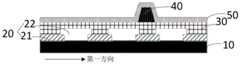
有鉴于此,在本发明的一个方面,本发明提供了一种彩膜基板。根据本发明的实施例,参照图1,所述彩膜基板包括:衬底10;彩膜层20,彩膜层20设置在所述衬底10的第一表面上,包括同层设置的黑矩阵21和彩色滤光片22;覆盖层30,所述覆盖层30设置在所述彩膜层20远离所述衬底10的表面上;隔垫物40,所述隔垫物40设置在所述覆盖层30远离所述衬底10的表面上;电极50,所述电极50设置在所述覆盖层30远离所述衬底10的表面上,且覆盖所述隔垫物40。发明人发现,将隔垫物直接设置在覆盖层表面粘附力较强,使得隔垫物能够牢固的贴附在覆盖层表面上且不易脱落,提高产品良率,并且上述彩膜基板的结构简单,易于实现,成本较低,且电极能够有效起到保护隔垫物和导电的作用。In view of this, in one aspect of the present invention, the present invention provides a color filter substrate. According to an embodiment of the present invention, referring to FIG. 1 , the color filter substrate includes: a
根据本发明的实施例,形成覆盖层的材料没有特别限制,只要能够有效覆盖彩膜层并且使得远离彩膜层的表面平坦,本领域技术人员可以根据实际需要灵活选择。例如形成覆盖层的材料可以包括但不限于树脂(resin)、硅-玻璃层合材料(SOG)或者苯并环丁烯(BCB)等,其中树脂可以包括光学胶等。According to the embodiments of the present invention, the material for forming the cover layer is not particularly limited, as long as it can effectively cover the color filter layer and make the surface away from the color filter layer flat, those skilled in the art can flexibly select according to actual needs. For example, the material for forming the cover layer may include but not limited to resin, silicon-glass laminate (SOG), benzocyclobutene (BCB), etc., wherein the resin may include optical glue and the like.
根据本发明的实施例,形成隔垫物的材料没有特别限制,只要能够有效起到支撑作用或者具有合适的力学性能,本领域技术人员可以根据实际需要灵活选择。例如形成隔垫物的材料可以包括但不限于聚酰亚胺或者树脂等,由此,材料来源广泛,弹性较佳,支撑效果较佳。According to the embodiment of the present invention, the material for forming the spacer is not particularly limited, as long as it can effectively play a supporting role or have suitable mechanical properties, those skilled in the art can flexibly select it according to actual needs. For example, the material for forming the spacer may include, but is not limited to, polyimide or resin, etc. Therefore, the material source is wide, the elasticity is better, and the support effect is better.
根据本发明的实施例,形成隔垫物与覆盖层的材料均可以为有机材料,因此二者的性质类似,根据相似相容的原理,将隔垫物直接设置在覆盖层的表面,由此隔垫物与覆盖层之间的粘附力较强,能够有效避免隔垫物的脱落,提高产品良率。According to the embodiment of the present invention, the materials for forming the spacer and the cover layer can be organic materials, so the properties of the two are similar. According to the principle of similar compatibility, the spacer is directly disposed on the surface of the cover layer, thereby The adhesive force between the spacer and the cover layer is strong, which can effectively prevent the spacer from falling off and improve the product yield.
根据本发明的实施例,隔垫物的形状没有特别限制,只要能够有效起到支撑作用,本领域技术人员可以根据实际需要灵活选择。例如隔垫物的形状可以为柱状,由此,隔垫物的支撑效果较佳,并能够使盒厚比较均匀。根据本发明的实施例,隔垫物的数量也没有特别限制,只要支撑效果较佳,本领域技术人员可以根据实际需要灵活选择。According to the embodiment of the present invention, the shape of the spacer is not particularly limited, as long as it can effectively play a supporting role, those skilled in the art can flexibly select it according to actual needs. For example, the shape of the spacer can be columnar, so that the support effect of the spacer is better, and the cell thickness can be relatively uniform. According to the embodiment of the present invention, the number of spacers is not particularly limited, and as long as the support effect is good, those skilled in the art can flexibly choose according to actual needs.
根据本发明的实施例,上述电极的种类没有特别限制,只要能够满足要求,本领域技术人员可以根据实际需要灵活选择。例如电极的种类可以包括但不限于透明金属电极、透明金属氧化物电极或者二者的组合或者不透明金属电极等。According to the embodiments of the present invention, the types of the above-mentioned electrodes are not particularly limited, and those skilled in the art can flexibly select them according to actual needs as long as they can meet the requirements. For example, the types of electrodes may include, but are not limited to, transparent metal electrodes, transparent metal oxide electrodes, or a combination of the two, or opaque metal electrodes, and the like.
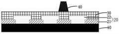
根据本发明的实施例,透明电极的结构没有特别限制,只要能够满足要求,本领域技术人员可以根据实际需要灵活选择。在本发明的一些实施例中,参照图2和图3,所述电极50包括:透明导电氧化物电极51和金属电极52,所述透明导电氧化物电极51设置在所述覆盖层30远离所述衬底10的表面上,且覆盖所述隔垫物40;所述金属电极52设置在所述透明导电氧化物电极51远离所述衬底10的表面上。由此,结构简单,易于实现,且可以使得透明电极兼具较高的透光率和较佳的导电性能,并能有效保护隔垫物,且由于金属电极与透明导电氧化物电极的性质类似,将金属电极设置在透明导电氧化物电极的表面上粘附性较佳,不易脱落,二者结合的比较紧密、牢固,使得产品的良率较高,并可以简化工艺,成本较低,使用性能较佳。According to the embodiment of the present invention, the structure of the transparent electrode is not particularly limited, and as long as it can meet the requirements, those skilled in the art can flexibly choose according to actual needs. In some embodiments of the present invention, referring to FIG. 2 and FIG. 3 , the
根据本发明的实施例,形成透明导电氧化物电极的材料没有特别限制,只要能够有效导电,本领域技术人员可以根据实际需要灵活选择。例如形成透明导电氧化物电极的材料可以包括但不限于铝掺杂的氧化锌(AZO)、氧化铝锌锡(AZTO)、氧化铟锡(ITO)或者掺杂氟的二氧化锡(FTO)等。According to the embodiments of the present invention, the material for forming the transparent conductive oxide electrode is not particularly limited, as long as it can conduct electricity effectively, those skilled in the art can flexibly select it according to actual needs. For example, the material for forming the transparent conductive oxide electrode may include, but is not limited to, aluminum-doped zinc oxide (AZO), aluminum-zinc-tin (AZTO), indium-tin-oxide (ITO), or fluorine-doped tin dioxide (FTO), etc. .
根据本发明的实施例,金属电极的结构没有特别限制,只要能够满足要求,本领域技术人员可以根据实际需要灵活选择。在本发明的一些实施例中,参照图3,所述金属电极52由一个第一透明金属面电极522构成;由此,结构简单,易于实现,导电性能较佳,使用性能较佳。在本发明的另一些实施例中,参照图2,所述金属电极52由多个在第一方向上间隔设置的子金属电极521构成。由此,结构简单,易于实现,导电性能较佳,且间隔设置的子金属电极能够使光线的透过率较大,使用性能较佳。According to the embodiment of the present invention, the structure of the metal electrode is not particularly limited, as long as it can meet the requirements, those skilled in the art can flexibly choose according to actual needs. In some embodiments of the present invention, referring to FIG. 3 , the
根据本发明的实施例,形成金属电极的材料没有特别限制,只要能够满足要求,本领域技术人员可以根据实际需要灵活选择,当金属电极由第一透明金属面电极构成时,形成金属电极的材料可以包括但不限于Ag、Al、Mg、Ca、Sm、Ba等,或其合金如Mg/Ag,Ca/Ag,Sm/Ag,Al/Ag,Ba/Ag等;由此,材料来源广泛,工艺容限较大,上述材料的导电性能较佳,使用性能较好。当金属电极由多个在第一方向上间隔设置的子金属电极521构成时,形成金属电极的材料可以包括但不限于Mo、Al、Ti、Au、Cu、Hf、Ta等常用金属,或其合金如AlNd,MoNb等,也可为多层金属如MoNb/Cu/MoNb、AlNd/Mo/AlNd等,由此,材料来源广泛,工艺容限较大。According to the embodiment of the present invention, the material for forming the metal electrode is not particularly limited, as long as the material can meet the requirements, those skilled in the art can flexibly choose according to actual needs. When the metal electrode is composed of the first transparent metal surface electrode, the material for forming the metal electrode Can include but not limited to Ag, Al, Mg, Ca, Sm, Ba, etc., or alloys thereof such as Mg/Ag, Ca/Ag, Sm/Ag, Al/Ag, Ba/Ag, etc.; The process tolerance is large, the electrical conductivity of the above-mentioned materials is better, and the use performance is better. When the metal electrode is composed of a plurality of
根据本发明的实施例,上述子金属电极可以为透明电极也可以为不透明电极,且当子金属电极为不透明电极时可以采用Cu金属制程,以利于降低金属走线电阻。According to the embodiment of the present invention, the above-mentioned sub-metal electrodes can be transparent electrodes or opaque electrodes, and when the sub-metal electrodes are opaque electrodes, Cu metal process can be used to help reduce metal wiring resistance.
根据本发明的实施例,为了提高显示质量并且不影响光的射出,参照图2,所述黑矩阵21在所述衬底10上的正投影覆盖所述子金属电极521在所述衬底10上的正投影。由此,子金属电极不会影响光线的射出,并且导电性能良好,有效提高显示质量,使用性能较佳。According to an embodiment of the present invention, in order to improve the display quality and not affect the light output, referring to FIG. 2 , the orthographic projection of the
在本发明的另一些实施例中,参照图4,所述电极50由一个第二透明金属面电极523构成,所述第二透明金属面电极523设置在所述覆盖层30远离所述衬底10的表面上,且覆盖所述隔垫物40。由此,结构简单,易于实现,并且能够起到保护隔垫物和导电的作用。In other embodiments of the present invention, referring to FIG. 4 , the
根据本发明的实施例,形成第二透明金属面电极的材料没有特别限制,只要能够满足要求,本领域技术人员可以根据实际需要灵活选择,例如形成第二透明金属面电极的材料可以包括但不限于Ag、Al、Mg、Ca、Sm、Ba等,或其合金如Mg/Ag,Ca/Ag,Sm/Ag,Al/Ag,Ba/Ag等;由此,材料来源广泛,工艺容限较大,且上述材料导电性能良好,使用性能较佳。According to the embodiment of the present invention, the material for forming the second transparent metal surface electrode is not particularly limited, as long as it can meet the requirements, those skilled in the art can flexibly choose according to actual needs, for example, the material for forming the second transparent metal surface electrode may include but not Limited to Ag, Al, Mg, Ca, Sm, Ba, etc., or their alloys such as Mg/Ag, Ca/Ag, Sm/Ag, Al/Ag, Ba/Ag, etc.; therefore, the material sources are wide and the process tolerance is relatively high Large, and the above-mentioned materials have good electrical conductivity and good performance.
根据本发明的实施例,为了有效防止漏光现象以及实现彩色显示,在彩膜层中设置有黑矩阵和彩色滤光片,参照图1,所述黑矩阵21限定出多个开口区域,所述彩色滤光片22设置在所述开口区域,且覆盖所述黑矩阵21的边缘。将彩色滤光片覆盖黑矩阵的边缘使得透过开口区域的光能够有效经过彩色滤光片22的过滤,可以降低漏光现象,提高含有上述彩膜基板的显示装置的显示质量,体高消费者的消费体验。According to an embodiment of the present invention, in order to effectively prevent light leakage and realize color display, a black matrix and a color filter are arranged in the color filter layer. Referring to FIG. 1 , the
根据本发明的实施例,参照图1,所述黑矩阵21在所述衬底上10的正投影覆盖所述隔垫物40在所述衬底10上的正投影,且在第一方向上,所述隔垫物40的宽度小于相邻两个所述开口区域之间的距离。由于隔垫物的宽度小于相邻两个开口区域之间的距离,使得光的透过不受隔垫物的影响,透过率较高,使用性能较佳。According to an embodiment of the present invention, referring to FIG. 1 , the orthographic projection of the
根据本发明的实施例,形成黑矩阵的材料没有特别限制,只要能够有效避免漏光现象,本领域技术人员可以根据实际需要灵活选择。例如形成黑矩阵的材料可以包括但不限于掺入黑色颜料的树脂、金属或者掺杂有金属或者碳的光刻胶等。According to the embodiment of the present invention, the material for forming the black matrix is not particularly limited, as long as the light leakage phenomenon can be effectively avoided, those skilled in the art can flexibly select according to actual needs. For example, the material forming the black matrix may include, but is not limited to, resin doped with black pigment, metal, or photoresist doped with metal or carbon, and the like.
根据本发明的实施例,彩色滤光片的颜色和排布方式没有特别限制,只要能够满足显示要求,本领域技术人员可以根据实际需要灵活选择。例如彩色滤光片的颜色可以包括红色、蓝色、绿色、黄色和透明的等;不同颜色的彩色滤光片的分布方式也没有特别限制,只要能够有效实现彩色显示,本领域技术人员可以根据实际需要灵活选择。According to the embodiments of the present invention, the color and arrangement of the color filters are not particularly limited, as long as the display requirements can be met, those skilled in the art can flexibly select them according to actual needs. For example, the colors of the color filters can include red, blue, green, yellow, transparent, etc.; the distribution mode of the color filters of different colors is not particularly limited, as long as the color display can be effectively realized, those skilled in the art can Flexibility is actually required.
根据本发明的实施例,形成衬底的材料没有特别限制,只要能够满足透光要求,本领域技术人员可以根据实际需要灵活选择。例如形成衬底的材料可以包括但不限于玻璃、透明金属、树脂或者聚酰亚胺等。According to the embodiments of the present invention, the material for forming the substrate is not particularly limited, as long as it can meet the requirement of light transmission, those skilled in the art can flexibly select it according to actual needs. For example, the material forming the substrate may include, but is not limited to, glass, transparent metal, resin, polyimide, and the like.
在本发明的另一方面,本发明提供了一种显示装置。根据本发明的实施例,所述显示装置包括前面所述的彩膜基板。所述显示装置含有前面所述的彩膜基板的全部特征和优点,在此不再过多赘述,并且所述显示装置的显示质量较佳,使用性能较佳。In another aspect of the present invention, the present invention provides a display device. According to an embodiment of the present invention, the display device includes the aforementioned color filter substrate. The display device includes all the features and advantages of the aforementioned color filter substrate, which will not be repeated here, and the display device has better display quality and better usability.
根据本发明的实施例,上述显示装置除了包括前面所述的彩膜基板之外,还包括一般显示装置应该具备的结构,例如阵列基板、OLED显示器件或液晶、电路或者封装层等。根据本发明的实施例,上述显示装置的类型可以为电脑、电视、手机、平板电脑、可穿戴设备或者车载显示器等,应用较为广泛。According to an embodiment of the present invention, the above-mentioned display device includes, in addition to the aforementioned color filter substrate, structures that a general display device should have, such as an array substrate, an OLED display device or liquid crystal, a circuit or an encapsulation layer, and the like. According to an embodiment of the present invention, the type of the above-mentioned display device may be a computer, a TV, a mobile phone, a tablet computer, a wearable device, or a vehicle-mounted display, etc., which are widely used.
在本发明的再一方面,本发明提供了一种制备彩膜基板的方法。根据本发明的实施例,参照图5,所述方法包括:In yet another aspect of the present invention, the present invention provides a method for preparing a color filter substrate. According to an embodiment of the present invention, referring to FIG. 5 , the method includes:
S100:在衬底10的第一表面上形成彩膜层20,结构示意图可参见图6和图7。S100 : forming a
根据本发明的实施例,所述衬底与彩膜层与前面的描述一致,在此不再过多赘述。According to the embodiment of the present invention, the substrate and the color filter layer are the same as those described above, and details are not repeated here.
需要说明的是,上述衬底的第一表面为使用时面向用户的表面。It should be noted that the first surface of the above-mentioned substrate is the surface facing the user during use.
根据本发明的实施例,形成彩膜层包括形成黑色矩阵和彩色滤光片的步骤,形成黑矩阵的步骤可以在形成彩色滤光片之前进行,只要能够满足彩色滤光片能够覆盖黑矩阵的边缘的要求即可。其中,形成黑色矩阵或者彩色滤光片的方式没有特别限制,只要能够满足要求,本领域技术人员可以根据实际需要灵活选择,例如形成黑色矩阵的或者彩色滤光片的方式各自可以独立的为溅射、涂覆、印刷、喷墨、电镀或者光刻等。According to an embodiment of the present invention, forming the color filter layer includes the steps of forming a black matrix and a color filter, and the step of forming the black matrix may be performed before forming the color filter, as long as the color filter can cover the black matrix. border requirements. Among them, the method of forming the black matrix or the color filter is not particularly limited, as long as the requirements can be met, those skilled in the art can flexibly choose according to the actual needs, for example, the method of forming the black matrix or the color filter can be independently splashed injection, coating, printing, inkjet, electroplating or photolithography, etc.
S200:在所述彩膜层20远离所述衬底10的表面上形成覆盖层30,结构示意图可参见图8。S200 : forming a
根据本发明的实施例,上述覆盖层与前面描述的一致,在此不再过多赘述。According to the embodiment of the present invention, the above-mentioned covering layer is the same as that described above, and details are not repeated here.
根据本发明的实施例,形成覆盖层的方式没有特别限制,只要能够使覆盖层的表面比较平坦,本领域技术人员可以根据实际需要灵活选择。例如形成覆盖层的方式可以为将形成覆盖层的材料涂覆在彩膜层远离衬底的表面,经过加热或者光照使得材料硬化形成。According to the embodiment of the present invention, the manner of forming the cover layer is not particularly limited, as long as the surface of the cover layer can be made relatively flat, those skilled in the art can flexibly choose according to actual needs. For example, the cover layer may be formed by coating the material for forming the cover layer on the surface of the color filter layer away from the substrate, and heating or illuminating the material to harden the material.
S300:在所述覆盖层30远离所述衬底10的表面上形成隔垫物40,结构示意图可参见图9。S300 : forming a
根据本发明的实施例,上述隔垫物与前面的描述一致,在此不再过多赘述。According to the embodiment of the present invention, the above-mentioned spacer is consistent with the foregoing description, and details are not repeated here.
根据本发明的实施例,形成隔垫物的方式没有特别限制,只要能够使隔垫物有效粘附在覆盖层表面,本领域技术人员可以根据实际需要灵活选择。在本发明的一些实施例中,将形成隔垫物的方式可以先将形成隔垫物的材料设置在覆盖层远离衬底的表面上,然后经过光刻或者切割等方式形成隔垫物。According to the embodiment of the present invention, the manner of forming the spacer is not particularly limited, as long as the spacer can be effectively adhered to the surface of the cover layer, those skilled in the art can flexibly choose according to actual needs. In some embodiments of the present invention, the spacer may be formed by firstly disposing the material for forming the spacer on the surface of the cover layer away from the substrate, and then forming the spacer by photolithography or cutting.
S400:在所述覆盖层30远离所述衬底10的表面上形成覆盖所述隔垫物40的电极50,结构示意图可参见图1。S400 : forming an
由此,操作简单方便,易于实现,电极的导电性能较佳,使用性能较佳。Therefore, the operation is simple and convenient, and the realization is easy, and the electrical conductivity of the electrode is better, and the use performance is better.
根据本发明的实施例,上述电极与前面的描述一致,在此不再过多赘述。According to the embodiment of the present invention, the above-mentioned electrodes are consistent with the foregoing descriptions, and details are not repeated here.
根据本发明的实施例,形成电极的方式没有特别限制,只要能够使电极导电,本领域技术人员可以根据实际需要灵活选择,例如形成电极的方式可以为淀积、溅射、印刷或者涂覆等。According to the embodiments of the present invention, the method of forming the electrode is not particularly limited, as long as the electrode can be made conductive, those skilled in the art can flexibly choose according to actual needs, for example, the method of forming the electrode can be deposition, sputtering, printing or coating, etc. .
发明人发现,采用上述方法制备彩膜基板操作简单方便,易于实现,并且将隔垫物形成在覆盖层的表面,可以使其与覆盖层的结合比较紧密,粘附力较强,隔垫物不容易脱落,提高产品良率,节约成本。The inventors found that using the above method to prepare the color filter substrate is simple, convenient and easy to implement, and the spacer is formed on the surface of the cover layer, so that the combination with the cover layer can be relatively tight, the adhesion is strong, and the spacer is formed. Not easy to fall off, improve product yield and save costs.
根据本发明的实施例,形成所述电极的方法包括:在所述覆盖层30远离所述衬底10的表面上形成覆盖所述隔垫物40的透明导电氧化物电极51;在所述透明导电氧化物电极51远离所述衬底10的表面上形成金属电极52,结构示意图可参照图1。由此,操作简单方便,易于实现,金属电极在透明导电氧化物电极的表面粘附力较强,不易脱落,产品良率较高,且将金属电极设置在透明导电氧化物电极的表面有利于提高导电性,提高显示装置的显示质量。According to an embodiment of the present invention, the method of forming the electrode includes: forming a transparent
根据本发明的实施例,所述透明导电氧化物电极以及金属电极与前面的描述一致,在此不再过多赘述。根据本发明的实施例,形成透明导电氧化电极的方式没有特别限制,可以包括但不限于淀积、溅射、印刷或者涂覆等,形成金属电极的方式也没有特别限制,可以包括但不限于淀积、溅射、刻蚀或者涂覆等,只要能够满足要求,本领域技术人员可以根据实际需要灵活选择。According to the embodiment of the present invention, the transparent conductive oxide electrode and the metal electrode are the same as those described above, which will not be repeated here. According to the embodiment of the present invention, the method of forming the transparent conductive oxide electrode is not particularly limited, which may include but not limited to deposition, sputtering, printing or coating, etc. The method of forming the metal electrode is also not particularly limited, and may include but not limited to Deposition, sputtering, etching or coating, etc., as long as the requirements can be met, those skilled in the art can flexibly choose according to actual needs.
根据本发明的实施例,在一般的显示装置中,其中的彩膜基板中的隔垫物设置在金属电极上,金属电极设置在覆盖层上,由于隔垫物与金属电极之间以及金属电极与覆盖层的结合能力较差,导致隔垫物和金属电极比较容易脱落,使得产品的良率较低,降低显示装置的显示质量,进而限制其应用。而在本申请中,利用了形成隔垫物与覆盖层以及形成透明导电氧化物电极和金属电极的材料的性质相似的特点,根据相似相容的原理,将隔垫物设置在覆盖层上,将金属电极设置在透明导电氧化物电极上,有效使得覆盖层与隔垫物或者金属电极与透明导电氧化物电极粘结在一起,使得隔垫物或者金属电极不容易脱落,提高产品良率,并且工艺简单,有效节约了成本。According to an embodiment of the present invention, in a general display device, the spacers in the color filter substrate are arranged on the metal electrodes, and the metal electrodes are arranged on the cover layer. The poor bonding ability with the cover layer causes the spacer and the metal electrode to fall off easily, resulting in a low product yield, lowering the display quality of the display device, and further limiting its application. In the present application, the characteristics of the similar properties of the materials forming the spacer and the cover layer and the materials forming the transparent conductive oxide electrode and the metal electrode are utilized, and the spacer is arranged on the cover layer according to the principle of similarity and compatibility, The metal electrode is arranged on the transparent conductive oxide electrode, which effectively makes the cover layer and the spacer or the metal electrode and the transparent conductive oxide electrode bond together, so that the spacer or the metal electrode is not easy to fall off, and the product yield is improved. In addition, the process is simple, and the cost is effectively saved.
下面根据本发明的具体示例,详细描述本发明的制备彩膜基板的方法,具体如下:The method for preparing a color filter substrate of the present invention will be described in detail below according to specific examples of the present invention, as follows:
实施例1:Example 1:
在本实施例中,参照图6至图9和图2,其中,电极50包括透明导电氧化物电极51以及在第一方向上间隔设置的子金属电极521,制备彩膜基板的方法如下:In this embodiment, referring to FIG. 6 to FIG. 9 and FIG. 2 , wherein the
1.对玻璃衬底10进行清洗,在衬底10上连续沉积黑矩阵21、彩色滤光片22、覆盖层30,其中彩色滤光片22制备时先后沉积R、G、B各彩膜,并使彩色滤光片22对黑矩阵21有一定的覆盖;1. The
2.沉积隔垫物40材料并形成图形,使隔垫物40图形位于挡光金属图形(或者黑矩阵21图形)的正上方,且图形的宽度要略小于黑矩阵21图形的宽度;2. Deposit the
3.淀积一层透明导电氧化物电极51薄膜,其中透明导电氧化物材料可为ITO、AZO、IZO、AZTO等材料,或这几种材料的组合如AZO/ITO等;3. Deposit a layer of transparent
4.最后淀积金属电极521,图形化后形成间隔设置的子金属电极,其材料可为Mo、Al、Ti、Au、Cu、Hf、Ta等常用金属,或其合金如AlNd,MoNb等,也可为多层金属如MoNb/Cu/MoNb、AlNd/Mo/AlNd等。4. Finally,
实施例2:Example 2:
在本实施例中,参照图6至图9和图3,其中,电极50包括透明导电氧化物电极51以及第一透明金属面电极522,制备彩膜基板的方法如下:In this embodiment, referring to FIG. 6 to FIG. 9 and FIG. 3, the
1.对玻璃衬底10进行清洗,在衬底10上连续沉积黑矩阵21、彩色滤光片22、覆盖层30,其中彩色滤光片22层制备时先后沉积R、G、B各彩膜,并使彩色滤光片22对黑矩阵21有一定的覆盖;1. The
2.沉积隔垫物40层材料并形成图形,使隔垫物40图形位于黑矩阵21图形的正上方,且图形的宽度要略小于黑矩阵21图形的宽度;2. Deposit the
3.最后淀积一层透明导电氧化物电极51薄膜和一薄层透明金属电极522,其中透明导电氧化物材料可为ITO、AZO、IZO、AZTO等常用材料,或这几种材料的组合如AZO/ITO等;透明金属电极材料可为Ag、Al、Mg、Ca、Sm等,或其合金如Ca/Ag,Sm/Ag,Al/Ag等。3. Finally, deposit a layer of transparent
实施例3:Example 3:
在本实施例中,参照图6至图9和图4,其中,电极50包括一个第二透明金属面电极523,制备彩膜基板的方法如下:In this embodiment, referring to FIG. 6 to FIG. 9 and FIG. 4, the
1.对玻璃衬底10进行清洗,在衬底上连续沉积黑矩阵21、彩色滤光片22、覆盖层30,其中彩色滤光片22层制备时先后沉积R、G、B各彩膜,并使彩色滤光片22对黑矩阵21有一定的覆盖;1. The
2.沉积隔垫物40层材料并形成图形,使隔垫物40图形位于黑矩阵22图形的正上方,且图形的宽度要略小于黑矩阵22图形的宽度;2. Deposit the
3.最后淀积一薄层透明金属电极523,其材料可为Ag、Al、Mg、Ca、Sm等,或其合金如Ca/Ag,Sm/Ag,Al/Ag等。3. Finally, a thin layer of
在本发明的描述中,需要理解的是,术语“中心”、“纵向”、“横向”、“长度”、“宽度”、“厚度”、“上”、“下”、“前”、“后”、“左”、“右”、“竖直”、“水平”、“顶”、“底”“内”、“外”、“顺时针”、“逆时针”、“轴向”、“径向”、“周向”等指示的方位或位置关系为基于附图所示的方位或位置关系,仅是为了便于描述本发明和简化描述,而不是指示或暗示所指的装置或元件必须具有特定的方位、以特定的方位构造和操作,因此不能理解为对本发明的限制。In the description of the present invention, it should be understood that the terms "center", "longitudinal", "lateral", "length", "width", "thickness", "upper", "lower", "front", " Rear, Left, Right, Vertical, Horizontal, Top, Bottom, Inner, Outer, Clockwise, Counterclockwise, Axial, The orientation or positional relationship indicated by "radial direction", "circumferential direction", etc. is based on the orientation or positional relationship shown in the drawings, and is only for the convenience of describing the present invention and simplifying the description, rather than indicating or implying the indicated device or element It must have a specific orientation, be constructed and operate in a specific orientation, and therefore should not be construed as a limitation of the present invention.
此外,术语“第一”、“第二”仅用于描述目的,而不能理解为指示或暗示相对重要性或者隐含指明所指示的技术特征的数量。由此,限定有“第一”、“第二”的特征可以明示或者隐含地包括一个或者更多个该特征。在本发明的描述中,“多个”的含义是两个或两个以上,除非另有明确具体的限定。In addition, the terms "first" and "second" are only used for descriptive purposes, and should not be construed as indicating or implying relative importance or implying the number of indicated technical features. Thus, a feature defined as "first" or "second" may expressly or implicitly include one or more of that feature. In the description of the present invention, "plurality" means two or more, unless otherwise expressly and specifically defined.
在本发明中,除非另有明确的规定和限定,术语“安装”、“相连”、“连接”、“固定”等术语应做广义理解,例如,可以是固定连接,也可以是可拆卸连接,或成一体;可以是机械连接,也可以是电连接;可以是直接相连,也可以通过中间媒介间接相连,可以是两个元件内部的连通或两个元件的相互作用关系。对于本领域的普通技术人员而言,可以根据具体情况理解上述术语在本发明中的具体含义。In the present invention, unless otherwise expressly specified and limited, the terms "installed", "connected", "connected", "fixed" and other terms should be understood in a broad sense, for example, it may be a fixed connection or a detachable connection , or integrated; it can be a mechanical connection or an electrical connection; it can be a direct connection or an indirect connection through an intermediate medium, and it can be the internal connection of the two elements or the interaction relationship between the two elements. For those of ordinary skill in the art, the specific meanings of the above terms in the present invention can be understood according to specific situations.
在本发明中,除非另有明确的规定和限定,第一特征在第二特征“上”或“下”可以是第一和第二特征直接接触,或第一和第二特征通过中间媒介间接接触。而且,第一特征在第二特征“之上”、“上方”和“上面”可是第一特征在第二特征正上方或斜上方,或仅仅表示第一特征水平高度高于第二特征。第一特征在第二特征“之下”、“下方”和“下面”可以是第一特征在第二特征正下方或斜下方,或仅仅表示第一特征水平高度小于第二特征。In the present invention, unless otherwise expressly specified and limited, a first feature "on" or "under" a second feature may be in direct contact between the first and second features, or the first and second features indirectly through an intermediary touch. Also, the first feature being "above", "over" and "above" the second feature may mean that the first feature is directly above or obliquely above the second feature, or simply means that the first feature is level higher than the second feature. The first feature being "below", "below" and "below" the second feature may mean that the first feature is directly or obliquely below the second feature, or simply means that the first feature has a lower level than the second feature.
在本说明书的描述中,参考术语“一个实施例”、“一些实施例”、“示例”、“具体示例”、或“一些示例”等的描述意指结合该实施例或示例描述的具体特征、结构、材料或者特点包含于本发明的至少一个实施例或示例中。在本说明书中,对上述术语的示意性表述不必须针对的是相同的实施例或示例。而且,描述的具体特征、结构、材料或者特点可以在任一个或多个实施例或示例中以合适的方式结合。此外,在不相互矛盾的情况下,本领域的技术人员可以将本说明书中描述的不同实施例或示例以及不同实施例或示例的特征进行结合和组合。In the description of this specification, description with reference to the terms "one embodiment," "some embodiments," "example," "specific example," or "some examples", etc., mean specific features described in connection with the embodiment or example , structure, material or feature is included in at least one embodiment or example of the present invention. In this specification, schematic representations of the above terms are not necessarily directed to the same embodiment or example. Furthermore, the particular features, structures, materials or characteristics described may be combined in any suitable manner in any one or more embodiments or examples. Furthermore, those skilled in the art may combine and combine the different embodiments or examples described in this specification, as well as the features of the different embodiments or examples, without conflicting each other.
尽管上面已经示出和描述了本发明的实施例,可以理解的是,上述实施例是示例性的,不能理解为对本发明的限制,本领域的普通技术人员在本发明的范围内可以对上述实施例进行变化、修改、替换和变型。Although the embodiments of the present invention have been shown and described above, it should be understood that the above embodiments are exemplary and should not be construed as limiting the present invention. Embodiments are subject to variations, modifications, substitutions and variations.
Claims (7)
Translated fromChinesePriority Applications (2)
| Application Number | Priority Date | Filing Date | Title |
|---|---|---|---|
| CN201711176769.9ACN107946345B (en) | 2017-11-22 | 2017-11-22 | Color filter substrate, preparation method thereof, and display device |
| US15/990,775US10727280B2 (en) | 2017-11-22 | 2018-05-28 | Substrate, method of manufacturing the same and display device |
Applications Claiming Priority (1)
| Application Number | Priority Date | Filing Date | Title |
|---|---|---|---|
| CN201711176769.9ACN107946345B (en) | 2017-11-22 | 2017-11-22 | Color filter substrate, preparation method thereof, and display device |
Publications (2)
| Publication Number | Publication Date |
|---|---|
| CN107946345A CN107946345A (en) | 2018-04-20 |
| CN107946345Btrue CN107946345B (en) | 2020-12-11 |
Family
ID=61929846
Family Applications (1)
| Application Number | Title | Priority Date | Filing Date |
|---|---|---|---|
| CN201711176769.9AActiveCN107946345B (en) | 2017-11-22 | 2017-11-22 | Color filter substrate, preparation method thereof, and display device |
Country Status (2)
| Country | Link |
|---|---|
| US (1) | US10727280B2 (en) |
| CN (1) | CN107946345B (en) |
Families Citing this family (4)
| Publication number | Priority date | Publication date | Assignee | Title |
|---|---|---|---|---|
| CN110164909B (en)* | 2018-04-24 | 2021-03-16 | 京东方科技集团股份有限公司 | Display substrate, preparation method thereof and display device |
| CN109244276A (en)* | 2018-09-06 | 2019-01-18 | 深圳市华星光电技术有限公司 | Organic Light Emitting Diode drives backboard manufacturing method |
| KR102832622B1 (en)* | 2021-01-04 | 2025-07-09 | 동우 화인켐 주식회사 | Mesh-patterned Touch Panel and Laminated Member therewith |
| CN118369614A (en)* | 2022-11-17 | 2024-07-19 | 京东方科技集团股份有限公司 | A display substrate, a manufacturing method thereof, a display panel and a display device |
Citations (1)
| Publication number | Priority date | Publication date | Assignee | Title |
|---|---|---|---|---|
| US8455046B2 (en)* | 2004-11-11 | 2013-06-04 | Lg Display Co., Ltd. | Thin film patterning apparatus and method of fabricating color filter array substrate using the same |
Family Cites Families (11)
| Publication number | Priority date | Publication date | Assignee | Title |
|---|---|---|---|---|
| TW573190B (en)* | 2000-08-14 | 2004-01-21 | Samsung Electronics Co Ltd | Liquid crystal display and fabricating method thereof |
| CN1292301C (en)* | 2003-05-12 | 2006-12-27 | 友达光电股份有限公司 | Liquid crystal display with uniform common voltage and manufacturing method thereof |
| KR20050043221A (en)* | 2003-11-05 | 2005-05-11 | 엘지.필립스 엘시디 주식회사 | Color filter substrate and fabrication method thereof |
| KR20050049986A (en)* | 2003-11-24 | 2005-05-27 | 엘지.필립스 엘시디 주식회사 | Color filter sustrate and fabrication method thereof using back exposure |
| KR101033461B1 (en)* | 2003-12-23 | 2011-05-11 | 엘지디스플레이 주식회사 | Liquid crystal display device and manufacturing method thereof |
| US8772783B2 (en)* | 2004-10-14 | 2014-07-08 | Semiconductor Energy Laboratory Co., Ltd. | Display device |
| KR101492538B1 (en)* | 2008-09-12 | 2015-02-12 | 삼성디스플레이 주식회사 | Thin film transistor substrate and method of fabricating the same |
| KR101620531B1 (en)* | 2009-10-08 | 2016-05-13 | 삼성디스플레이 주식회사 | Liquid crystal display |
| KR101859478B1 (en)* | 2011-11-30 | 2018-06-29 | 엘지디스플레이 주식회사 | Liquid crystal display device having touch screen |
| JP2014174319A (en)* | 2013-03-08 | 2014-09-22 | Sony Corp | Display device and method for manufacturing display device, and electronic apparatus |
| CN103700688B (en) | 2013-12-23 | 2016-03-30 | 京东方科技集团股份有限公司 | Color membrane substrates and preparation method thereof, display unit |
- 2017
- 2017-11-22CNCN201711176769.9Apatent/CN107946345B/enactiveActive
- 2018
- 2018-05-28USUS15/990,775patent/US10727280B2/enactiveActive
Patent Citations (1)
| Publication number | Priority date | Publication date | Assignee | Title |
|---|---|---|---|---|
| US8455046B2 (en)* | 2004-11-11 | 2013-06-04 | Lg Display Co., Ltd. | Thin film patterning apparatus and method of fabricating color filter array substrate using the same |
Also Published As
| Publication number | Publication date |
|---|---|
| US10727280B2 (en) | 2020-07-28 |
| US20190157353A1 (en) | 2019-05-23 |
| CN107946345A (en) | 2018-04-20 |
Similar Documents
| Publication | Publication Date | Title |
|---|---|---|
| CN209691758U (en) | Display panel and display device | |
| CN107946345B (en) | Color filter substrate, preparation method thereof, and display device | |
| CN107193422B (en) | Array substrate, display panel and display device | |
| US9761816B2 (en) | Flexible organic light-emitting display device and method for manufacturing the same | |
| US20180069065A1 (en) | Display device | |
| CN110767841B (en) | Display substrate and preparation method thereof, and display device | |
| CN108550616B (en) | OLED display substrate, method for making the same, and display device | |
| CN106910765A (en) | A kind of electroluminescence display panel, its preparation method and display device | |
| CN107302016B (en) | Organic light-emitting diode display panel and manufacturing method thereof | |
| TW202201088A (en) | Display device and electronic device | |
| CN107706210A (en) | OLED display panel, the manufacture method of OLED display panel and display device | |
| CN207165572U (en) | A kind of array base palte and display device | |
| CN103969865A (en) | Thin film transistor (TFT) array substrate and process method thereof, display panel with same and display device with same | |
| CN110582850B (en) | Organic light emitting diode display panel, method of manufacturing the same, and organic light emitting diode counter substrate | |
| CN215494957U (en) | Touch panel and display touch device | |
| CN106896959A (en) | A kind of touch display screen and its manufacture method | |
| CN111490086A (en) | Display substrate, preparation method thereof and display device | |
| CN107731877A (en) | A kind of color membrane substrates, its preparation method and display device | |
| CN109300912A (en) | Display substrate based on electroluminescent device, preparation method thereof, and display device | |
| CN112310183B (en) | Display substrate and preparation method thereof, display device | |
| CN105607334A (en) | Array substrate and preparation method thereof, display panel and display device | |
| CN110098247A (en) | Show backboard and preparation method thereof and display device | |
| CN107845662A (en) | A kind of color membrane substrates and preparation method thereof and display device | |
| CN113555400A (en) | Display substrate and preparation method thereof, and display device | |
| CN114967958B (en) | Touch panel and manufacturing method thereof, and display touch device |
Legal Events
| Date | Code | Title | Description |
|---|---|---|---|
| PB01 | Publication | ||
| PB01 | Publication | ||
| SE01 | Entry into force of request for substantive examination | ||
| SE01 | Entry into force of request for substantive examination | ||
| GR01 | Patent grant | ||
| GR01 | Patent grant |