CN107923928B - Apparatus and method for inspecting the surface of a sample - Google Patents
Apparatus and method for inspecting the surface of a sampleDownload PDFInfo
- Publication number
- CN107923928B CN107923928BCN201680028920.1ACN201680028920ACN107923928BCN 107923928 BCN107923928 BCN 107923928BCN 201680028920 ACN201680028920 ACN 201680028920ACN 107923928 BCN107923928 BCN 107923928B
- Authority
- CN
- China
- Prior art keywords
- probe
- tip
- sample surface
- tips
- contact
- Prior art date
- Legal status (The legal status is an assumption and is not a legal conclusion. Google has not performed a legal analysis and makes no representation as to the accuracy of the status listed.)
- Expired - Fee Related
Links
- 238000000034methodMethods0.000titleclaimsdescription43
- 239000000523sampleSubstances0.000claimsabstractdescription348
- 230000008859changeEffects0.000claimsabstractdescription22
- 239000000758substrateSubstances0.000claimsabstractdescription22
- 238000005286illuminationMethods0.000claimsabstractdescription16
- 239000000463materialSubstances0.000claimsabstractdescription7
- 238000012876topographyMethods0.000claimsdescription27
- XUIMIQQOPSSXEZ-UHFFFAOYSA-NSiliconChemical compound[Si]XUIMIQQOPSSXEZ-UHFFFAOYSA-N0.000description42
- 239000010703siliconSubstances0.000description42
- 229910052710siliconInorganic materials0.000description41
- 238000000926separation methodMethods0.000description35
- 238000002474experimental methodMethods0.000description30
- 238000005259measurementMethods0.000description25
- 238000000399optical microscopyMethods0.000description25
- 239000004205dimethyl polysiloxaneSubstances0.000description23
- 229920000435poly(dimethylsiloxane)Polymers0.000description23
- 238000003384imaging methodMethods0.000description22
- 230000003287optical effectEffects0.000description18
- VYPSYNLAJGMNEJ-UHFFFAOYSA-NSilicium dioxideChemical compoundO=[Si]=OVYPSYNLAJGMNEJ-UHFFFAOYSA-N0.000description16
- QJAOYSPHSNGHNC-UHFFFAOYSA-Noctadecane-1-thiolChemical groupCCCCCCCCCCCCCCCCCCSQJAOYSPHSNGHNC-UHFFFAOYSA-N0.000description14
- 230000008569processEffects0.000description12
- 238000000386microscopyMethods0.000description11
- 230000005660hydrophilic surfaceEffects0.000description10
- 230000002209hydrophobic effectEffects0.000description9
- 235000012431wafersNutrition0.000description9
- 238000004630atomic force microscopyMethods0.000description8
- 238000004364calculation methodMethods0.000description8
- PCHJSUWPFVWCPO-UHFFFAOYSA-NgoldChemical compound[Au]PCHJSUWPFVWCPO-UHFFFAOYSA-N0.000description8
- 239000010931goldSubstances0.000description8
- 229910052737goldInorganic materials0.000description8
- 230000005661hydrophobic surfaceEffects0.000description8
- 230000033001locomotionEffects0.000description8
- 238000004621scanning probe microscopyMethods0.000description8
- 239000011521glassSubstances0.000description7
- 239000000203mixtureSubstances0.000description7
- 239000000377silicon dioxideSubstances0.000description7
- 235000012239silicon dioxideNutrition0.000description7
- KRHYYFGTRYWZRS-UHFFFAOYSA-NFluoraneChemical compoundFKRHYYFGTRYWZRS-UHFFFAOYSA-N0.000description6
- 229910052581Si3N4Inorganic materials0.000description6
- YXFVVABEGXRONW-UHFFFAOYSA-NTolueneChemical compoundCC1=CC=CC=C1YXFVVABEGXRONW-UHFFFAOYSA-N0.000description6
- 238000004458analytical methodMethods0.000description6
- 229920001971elastomerPolymers0.000description6
- 239000000806elastomerSubstances0.000description6
- 150000002343goldChemical class0.000description6
- HQVNEWCFYHHQES-UHFFFAOYSA-Nsilicon nitrideChemical compoundN12[Si]34N5[Si]62N3[Si]51N64HQVNEWCFYHHQES-UHFFFAOYSA-N0.000description6
- 238000004088simulationMethods0.000description6
- 239000000126substanceSubstances0.000description6
- 238000009826distributionMethods0.000description5
- 230000003993interactionEffects0.000description5
- 239000010410layerSubstances0.000description5
- -1polydimethylsiloxanePolymers0.000description5
- XLYOFNOQVPJJNP-UHFFFAOYSA-NwaterSubstancesOXLYOFNOQVPJJNP-UHFFFAOYSA-N0.000description5
- CSCPPACGZOOCGX-UHFFFAOYSA-NAcetoneChemical compoundCC(C)=OCSCPPACGZOOCGX-UHFFFAOYSA-N0.000description4
- LFQSCWFLJHTTHZ-UHFFFAOYSA-NEthanolChemical compoundCCOLFQSCWFLJHTTHZ-UHFFFAOYSA-N0.000description4
- MHAJPDPJQMAIIY-UHFFFAOYSA-NHydrogen peroxideChemical compoundOOMHAJPDPJQMAIIY-UHFFFAOYSA-N0.000description4
- QAOWNCQODCNURD-UHFFFAOYSA-NSulfuric acidChemical compoundOS(O)(=O)=OQAOWNCQODCNURD-UHFFFAOYSA-N0.000description4
- 229920002120photoresistant polymerPolymers0.000description4
- BASFCYQUMIYNBI-UHFFFAOYSA-NplatinumChemical compound[Pt]BASFCYQUMIYNBI-UHFFFAOYSA-N0.000description4
- 229920000642polymerPolymers0.000description4
- 238000012545processingMethods0.000description4
- 230000007704transitionEffects0.000description4
- WYTZZXDRDKSJID-UHFFFAOYSA-N(3-aminopropyl)triethoxysilaneChemical compoundCCO[Si](OCC)(OCC)CCCNWYTZZXDRDKSJID-UHFFFAOYSA-N0.000description3
- IJGRMHOSHXDMSA-UHFFFAOYSA-NAtomic nitrogenChemical compoundN#NIJGRMHOSHXDMSA-UHFFFAOYSA-N0.000description3
- 239000004594Masterbatch (MB)Substances0.000description3
- QVGXLLKOCUKJST-UHFFFAOYSA-Natomic oxygenChemical compound[O]QVGXLLKOCUKJST-UHFFFAOYSA-N0.000description3
- 238000011161developmentMethods0.000description3
- 238000001493electron microscopyMethods0.000description3
- 238000005530etchingMethods0.000description3
- 229910052751metalInorganic materials0.000description3
- 239000002184metalSubstances0.000description3
- SLYCYWCVSGPDFR-UHFFFAOYSA-NoctadecyltrimethoxysilaneChemical compoundCCCCCCCCCCCCCCCCCC[Si](OC)(OC)OCSLYCYWCVSGPDFR-UHFFFAOYSA-N0.000description3
- 239000001301oxygenSubstances0.000description3
- 229910052760oxygenInorganic materials0.000description3
- 238000000206photolithographyMethods0.000description3
- 238000011160researchMethods0.000description3
- 230000002441reversible effectEffects0.000description3
- 241000252506CharaciformesSpecies0.000description2
- KFZMGEQAYNKOFK-UHFFFAOYSA-NIsopropanolChemical compoundCC(C)OKFZMGEQAYNKOFK-UHFFFAOYSA-N0.000description2
- 238000013459approachMethods0.000description2
- 239000011248coating agentSubstances0.000description2
- 238000000576coating methodMethods0.000description2
- 230000007423decreaseEffects0.000description2
- 238000013461designMethods0.000description2
- 238000005516engineering processMethods0.000description2
- 238000009499grossingMethods0.000description2
- 238000001459lithographyMethods0.000description2
- 230000004807localizationEffects0.000description2
- 238000004519manufacturing processMethods0.000description2
- 230000005499meniscusEffects0.000description2
- 239000002086nanomaterialSubstances0.000description2
- 238000004651near-field scanning optical microscopyMethods0.000description2
- 229910052697platinumInorganic materials0.000description2
- 238000002360preparation methodMethods0.000description2
- 238000004574scanning tunneling microscopyMethods0.000description2
- 238000012360testing methodMethods0.000description2
- 238000004627transmission electron microscopyMethods0.000description2
- 229920002554vinyl polymerPolymers0.000description2
- 238000001039wet etchingMethods0.000description2
- VMAWODUEPLAHOE-UHFFFAOYSA-N2,4,6,8-tetrakis(ethenyl)-2,4,6,8-tetramethyl-1,3,5,7,2,4,6,8-tetraoxatetrasilocaneChemical compoundC=C[Si]1(C)O[Si](C)(C=C)O[Si](C)(C=C)O[Si](C)(C=C)O1VMAWODUEPLAHOE-UHFFFAOYSA-N0.000description1
- VYZAMTAEIAYCRO-UHFFFAOYSA-NChromiumChemical compound[Cr]VYZAMTAEIAYCRO-UHFFFAOYSA-N0.000description1
- 239000004971Cross linkerSubstances0.000description1
- CTQNGGLPUBDAKN-UHFFFAOYSA-NO-XyleneChemical compoundCC1=CC=CC=C1CCTQNGGLPUBDAKN-UHFFFAOYSA-N0.000description1
- 244000208734Pisonia aculeataSpecies0.000description1
- KWYUFKZDYYNOTN-UHFFFAOYSA-MPotassium hydroxideChemical compound[OH-].[K+]KWYUFKZDYYNOTN-UHFFFAOYSA-M0.000description1
- 230000009471actionEffects0.000description1
- 239000012080ambient airSubstances0.000description1
- 238000000347anisotropic wet etchingMethods0.000description1
- 238000003491arrayMethods0.000description1
- 238000000089atomic force micrographMethods0.000description1
- 238000000418atomic force spectrumMethods0.000description1
- 230000004888barrier functionEffects0.000description1
- 230000005540biological transmissionEffects0.000description1
- FSIJKGMIQTVTNP-UHFFFAOYSA-Nbis(ethenyl)-methyl-trimethylsilyloxysilaneChemical compoundC[Si](C)(C)O[Si](C)(C=C)C=CFSIJKGMIQTVTNP-UHFFFAOYSA-N0.000description1
- 230000000903blocking effectEffects0.000description1
- HQABUPZFAYXKJW-UHFFFAOYSA-Nbutan-1-amineChemical compoundCCCCNHQABUPZFAYXKJW-UHFFFAOYSA-N0.000description1
- 239000003054catalystSubstances0.000description1
- 238000004666chemical force microscopyMethods0.000description1
- 238000004140cleaningMethods0.000description1
- 239000003431cross linking reagentSubstances0.000description1
- 230000003247decreasing effectEffects0.000description1
- 238000010586diagramMethods0.000description1
- 229910001873dinitrogenInorganic materials0.000description1
- 238000000979dip-pen nanolithographyMethods0.000description1
- 230000000694effectsEffects0.000description1
- 238000010894electron beam technologyMethods0.000description1
- 238000001914filtrationMethods0.000description1
- 239000007789gasSubstances0.000description1
- 238000003706image smoothingMethods0.000description1
- 238000007689inspectionMethods0.000description1
- 230000007774longtermEffects0.000description1
- 238000012423maintenanceMethods0.000description1
- 238000000691measurement methodMethods0.000description1
- 238000000813microcontact printingMethods0.000description1
- 238000002156mixingMethods0.000description1
- 238000012544monitoring processMethods0.000description1
- 229910052757nitrogenInorganic materials0.000description1
- 239000012044organic layerSubstances0.000description1
- 230000000737periodic effectEffects0.000description1
- 230000010287polarizationEffects0.000description1
- 229920000307polymer substratePolymers0.000description1
- 229920001296polysiloxanePolymers0.000description1
- 229920006395saturated elastomerPolymers0.000description1
- 238000004626scanning electron microscopyMethods0.000description1
- 238000000263scanning probe lithographyMethods0.000description1
- 239000002094self assembled monolayerSubstances0.000description1
- 239000013545self-assembled monolayerSubstances0.000description1
- 239000004065semiconductorSubstances0.000description1
- 238000002444silanisationMethods0.000description1
- 229910052814silicon oxideInorganic materials0.000description1
- 238000000527sonicationMethods0.000description1
- 238000004528spin coatingMethods0.000description1
- 238000010857super resolution fluorescence microscopyMethods0.000description1
- 230000001360synchronised effectEffects0.000description1
- AKIOHULKHAVIMI-UHFFFAOYSA-Ntrichloro(1,1,2,2,3,3,4,4,5,5,6,6,7,7,8,8,9,9,10,10,11,11,12,12,12-pentacosafluorododecyl)silaneChemical compoundFC(F)(F)C(F)(F)C(F)(F)C(F)(F)C(F)(F)C(F)(F)C(F)(F)C(F)(F)C(F)(F)C(F)(F)C(F)(F)C(F)(F)[Si](Cl)(Cl)ClAKIOHULKHAVIMI-UHFFFAOYSA-N0.000description1
- 238000009849vacuum degassingMethods0.000description1
- 125000000391vinyl groupChemical group[H]C([*])=C([H])[H]0.000description1
- 239000008096xyleneSubstances0.000description1
Images


Classifications
- G—PHYSICS
- G01—MEASURING; TESTING
- G01Q—SCANNING-PROBE TECHNIQUES OR APPARATUS; APPLICATIONS OF SCANNING-PROBE TECHNIQUES, e.g. SCANNING PROBE MICROSCOPY [SPM]
- G01Q10/00—Scanning or positioning arrangements, i.e. arrangements for actively controlling the movement or position of the probe
- G01Q10/04—Fine scanning or positioning
- G01Q10/06—Circuits or algorithms therefor
- G01Q10/065—Feedback mechanisms, i.e. wherein the signal for driving the probe is modified by a signal coming from the probe itself
- G—PHYSICS
- G01—MEASURING; TESTING
- G01Q—SCANNING-PROBE TECHNIQUES OR APPARATUS; APPLICATIONS OF SCANNING-PROBE TECHNIQUES, e.g. SCANNING PROBE MICROSCOPY [SPM]
- G01Q20/00—Monitoring the movement or position of the probe
- G01Q20/02—Monitoring the movement or position of the probe by optical means
- G—PHYSICS
- G01—MEASURING; TESTING
- G01Q—SCANNING-PROBE TECHNIQUES OR APPARATUS; APPLICATIONS OF SCANNING-PROBE TECHNIQUES, e.g. SCANNING PROBE MICROSCOPY [SPM]
- G01Q60/00—Particular types of SPM [Scanning Probe Microscopy] or microscopes; Essential components thereof
- G01Q60/18—SNOM [Scanning Near-Field Optical Microscopy] or apparatus therefor, e.g. SNOM probes
- G01Q60/22—Probes, their manufacture, or their related instrumentation, e.g. holders
- G—PHYSICS
- G01—MEASURING; TESTING
- G01Q—SCANNING-PROBE TECHNIQUES OR APPARATUS; APPLICATIONS OF SCANNING-PROBE TECHNIQUES, e.g. SCANNING PROBE MICROSCOPY [SPM]
- G01Q70/00—General aspects of SPM probes, their manufacture or their related instrumentation, insofar as they are not specially adapted to a single SPM technique covered by group G01Q60/00
- G01Q70/06—Probe tip arrays
- G—PHYSICS
- G01—MEASURING; TESTING
- G01Q—SCANNING-PROBE TECHNIQUES OR APPARATUS; APPLICATIONS OF SCANNING-PROBE TECHNIQUES, e.g. SCANNING PROBE MICROSCOPY [SPM]
- G01Q70/00—General aspects of SPM probes, their manufacture or their related instrumentation, insofar as they are not specially adapted to a single SPM technique covered by group G01Q60/00
- G01Q70/08—Probe characteristics
- G01Q70/14—Particular materials
- G—PHYSICS
- G02—OPTICS
- G02B—OPTICAL ELEMENTS, SYSTEMS OR APPARATUS
- G02B21/00—Microscopes
- G02B21/0004—Microscopes specially adapted for specific applications
- G02B21/002—Scanning microscopes
Landscapes
- Physics & Mathematics (AREA)
- General Physics & Mathematics (AREA)
- Health & Medical Sciences (AREA)
- General Health & Medical Sciences (AREA)
- Nuclear Medicine, Radiotherapy & Molecular Imaging (AREA)
- Radiology & Medical Imaging (AREA)
- Chemical & Material Sciences (AREA)
- Analytical Chemistry (AREA)
- Optics & Photonics (AREA)
- Length Measuring Devices By Optical Means (AREA)
- Length Measuring Devices With Unspecified Measuring Means (AREA)
Abstract
Description
Translated fromChinese技术领域technical field
本发明实施方式涉及样品表面的检查和成像。具体而言,本发明实施方式涉及样品表面的形貌和表面化学等性质的测定。Embodiments of the present invention relate to inspection and imaging of sample surfaces. Specifically, the embodiments of the present invention relate to the determination of properties such as the topography and surface chemistry of the sample surface.
背景技术Background technique
纵观历史,显微技术领域的突破往往带来科学研究的突破性进展。例如,随着扫描隧道显微镜(STM),电子显微镜(EM)以及相关技术的发展,纳米技术已成为一种极有可能改变我们几十年前生活方式的新兴技术。第一台光学显微镜发明于400多年以前,它让我们看到了肉眼看不见的物体。直至今天,光学显微镜仍然是工业界和学术界最广泛使用的以下三类显微镜当中的一类:光学显微镜;电子显微镜(扫描电子显微镜(SEM)和透射电子显微镜(TEM) 均属此类);以及扫描探针显微镜(SPM)一族。光学显微镜(OM)的优点在于快速,大区域成像以及易于准备样品。然而,衍射屏障使得传统光学显微镜无法利用可见光区分尺寸小于200nm的纳米结构。Throughout history, breakthroughs in microscopy have often led to breakthroughs in scientific research. For example, with the development of scanning tunneling microscopy (STM), electron microscopy (EM), and related technologies, nanotechnology has emerged as an emerging technology that has the potential to change the way we live decades ago. Invented more than 400 years ago, the first optical microscope allowed us to see objects invisible to the naked eye. To this day, light microscopes are still one of the three most widely used types of microscopes in industry and academia: optical microscopes; electron microscopes (both Scanning Electron Microscopy (SEM) and Transmission Electron Microscopy (TEM)); and Scanning Probe Microscopy (SPM) family. The advantages of optical microscopy (OM) are fast, large area imaging and ease of sample preparation. However, the diffraction barrier makes it impossible for conventional optical microscopy to distinguish nanostructures smaller than 200 nm in size using visible light.
近场扫描光学显微术(NSOM)通过将针尖放置在被测样品感兴趣表面附近区域(针尖或纳米天线的10nm)的方式避开衍射极限。然而,其局限在于扫描面积较小。最近,超分辨率荧光显微术已成功突破衍射极限,此类显微术包括受激发射损耗(STED)或可逆饱和荧光跃迁(RESOLFT)显微术,光激活定位显微术(PALM)或荧光光激活定位显微术(FPALM),饱和结构照明显微术 (SSIM)以及随机光学重建显微术(STORM)。虽然这些技术已经在生命科学研究中实现了高至20nm的分辨率,但是由于其需要使用荧光基团,因此无法应用至硅基半导体等不能够由荧光基团进行标记的样品中。另一方面,电子显微镜采用短波长电子束照射样品,因此透射电子显微镜可实现高于50pm的分辨率。然而,其制造及维护费用较高。扫描隧道显微术及原子力显微镜(AFM) 等扫描探针显微镜利用物理探针直接触摸和感测样品表面,以获取其形貌图像和其他图像。因此,其可以以亚分子分辨率直接呈现包含形貌、化学、静电、磁性和热学性质等在内的各种表面性质。Near-field Scanning Optical Microscopy (NSOM) circumvents the diffraction limit by placing the tip in a region (10 nm of the tip or nanoantenna) near the surface of interest of the sample under test. However, its limitation is the small scanning area. Recently, super-resolution fluorescence microscopy has successfully broken the diffraction limit, such microscopy including stimulated emission depletion (STED) or reversible saturation fluorescence transition (RESOLFT) microscopy, photoactivated localization microscopy (PALM) or Fluorescence photoactivated localization microscopy (FPALM), saturated structured illumination microscopy (SSIM), and stochastic optical reconstruction microscopy (STORM). While these techniques have achieved resolutions up to 20 nm in life science research, they cannot be applied to samples such as silicon-based semiconductors that cannot be labeled with fluorophores because they require the use of fluorophores. Electron microscopy, on the other hand, uses a short wavelength electron beam to irradiate the sample, so transmission electron microscopy can achieve resolutions higher than 50pm. However, its manufacturing and maintenance costs are high. Scanning probe microscopes such as scanning tunneling microscopy and atomic force microscopy (AFM) use physical probes to directly touch and sense the surface of a sample to obtain topographic and other images of it. Therefore, it can directly present various surface properties including topographic, chemical, electrostatic, magnetic and thermal properties at sub-molecular resolution.
然而,扫描探针显微镜的关键问题在于扫描速度较慢,扫描尺寸较小,且场深度较小。举例而言,商业原子力显微镜需要若干分钟才能获得一张最大扫描尺寸小于80×80μm2的高质量图像。虽然早在15多年前已经开始开发旨在提高原子力显微镜扫描速度的高谐振频率悬臂式原子力显微镜,然而直至现在,单针尖式设计的串行处理特性使得其每次的扫描面积只能局限于40×40μm2之内。虽然现在已通过集成的压阻传感器和ZnO致动器实现了使用多针尖进行并行成像,然而其分辨率受到噪声的限制。此外,其复杂的设计和设置使得难以为大多数研究人员所用。因此,到目前为止,开发一种可在大面积(达毫米级别)内进行亚衍射分辨率形貌成像的简单成像技术仍然是一项难题。However, the key problems with scanning probe microscopy are the slow scan speed, small scan size, and small depth of field. For example, commercial atomic force microscopes take several minutes to obtain a high-quality image with a maximum scan size of less than 80 x 80 μm2. Although the development of high-resonance frequency cantilever AFMs aimed at increasing the scanning speed of AFMs began more than 15 years ago, until now, the serial processing nature of the single-tip design has limited the area of each scan to 40 Within ×40μm2. Although parallel imaging using multiple tips has now been achieved with integrated piezoresistive sensors and ZnO actuators, its resolution is limited by noise. Furthermore, its complex design and setup make it difficult to use for most researchers. Therefore, until now, developing a simple imaging technique capable of sub-diffractive resolution topography imaging over large areas (up to the millimeter scale) has remained a challenge.
近来发展的聚合物笔平版印刷术(PPL)将传统单针尖式浸蘸笔纳米平版印刷术的处理能力提高了三个数量级,该技术利用由数百个聚二甲基硅氧烷 (PDMS)针尖组成的针尖阵列在基板表面同时“写入”墨水。对于原子力显微镜,样品表面信息由柔性悬臂的偏转或扭转进行反映,通过对投射于悬臂背面的激光的微小运动的监测而对所述偏转或扭转进行检测。然而,该技术难以通过多个激光束实现多针尖并行成像,这是因为多个激光器可能在小的有限空间内彼此干扰。The recent development of polymer pen lithography (PPL) has improved the processing power of traditional single-needle-tip dip pen nanolithography by three orders of magnitude, utilizing hundreds of polydimethylsiloxane (PDMS) An array of needle tips simultaneously "writes" ink on the substrate surface. For atomic force microscopy, the sample surface information is reflected by the deflection or twisting of the flexible cantilever, which is detected by monitoring the tiny movements of the laser light projected on the back of the cantilever. However, this technique is difficult to achieve multi-tip parallel imaging with multiple laser beams because multiple lasers may interfere with each other in a small confined space.
由于显微术能为研究人员提供对微/纳米材料进行可视化和研究的智能“眼睛”,因此开发一种不受衍射极限限制且可进行大面积成像的简单显微术是纳米技术领域内的一项长期目标。虽然如上所述显微术的进步已使得许多领域内的科学研究产生了翻天覆地的变化,然而现有显微术仍不得不在处理能力,分辨率和所获得的样品表面信息之间进行权衡和折衷。Since microscopy provides researchers with intelligent "eyes" to visualize and study micro/nanomaterials, developing a simple microscopy that is not limited by the diffraction limit and can image large areas is within the realm of nanotechnology a long-term goal. Although advances in microscopy as described above have revolutionized scientific research in many fields, existing microscopy still has to make trade-offs and compromises between processing power, resolution, and obtained sample surface information .
发明内容SUMMARY OF THE INVENTION
根据本发明的第一方面,提供一种用于检查样品表面的装置。该装置包括:探针阵列,该探针阵列包括基底以及自该所述基底延伸而出的多个探针针尖,该探针针尖包括透明且可变形的材料并用于接触所述样品表面;用于将所述探针阵列朝所述样品表面移动的致动器;用于通过透过所述基底的照明光对所述探针针尖进行照明的光源;以及用于检测从所述探针针尖反射的照明光的强度变化的图像捕获装置。According to a first aspect of the present invention, there is provided an apparatus for inspecting the surface of a sample. The device includes: a probe array comprising a substrate and a plurality of probe tips extending from the substrate, the probe tips comprising a transparent and deformable material and for contacting the sample surface; an actuator for moving the probe array toward the sample surface; a light source for illuminating the probe tips by illuminating light through the substrate; and a light source for detecting transmission from the probe tips An image capture device in which the intensity of reflected illumination light varies.
本发明实施方式提供一种新的成像技术,称为并行扫描光学显微术(ParallelScanning Optical Microscopy,PSOM)。本发明实施方式可利用具有多达91个针尖的针尖阵列获取0.15平方毫米区域的亚衍射分辨率形貌图像。并行扫描光学显微术融合了现有光学显微术的大面积成像优点和扫描探针显微术的高垂直分辨率。在实施方式中,并行扫描光学显微术采用弹性体针尖顶点处的白光反射光强变化(灰度变化)作为反馈信号,对表面信息进行探究,从而实现针尖阵列在毫米级区域上的同步并行扫描。除了以现有的30nm垂直分辨率进行形貌成像之外,其还可使所述弹性针尖具有获取表面化学等其他表面信息的功能。Embodiments of the present invention provide a new imaging technique called Parallel Scanning Optical Microscopy (PSOM). Embodiments of the present invention may utilize tip arrays with up to 91 tips to acquire sub-diffraction resolution topography images of a 0.15 square millimeter area. Parallel scanning optical microscopy combines the large-area imaging advantages of existing optical microscopy with the high vertical resolution of scanning probe microscopy. In an embodiment, parallel scanning optical microscopy uses the reflected light intensity change (grayscale change) of the white light at the apex of the elastomer tip as a feedback signal to explore the surface information, thereby realizing the synchronous parallelism of the tip array on a millimeter-scale area scanning. In addition to topographic imaging with the existing 30 nm vertical resolution, it can also enable the elastic tip to acquire other surface information such as surface chemistry.
在一种实施方式中,所述探针针尖包括弹性体。该探针针尖可包括聚二甲基硅氧烷(PDMS)。In one embodiment, the probe tip includes an elastomer. The probe tip may comprise polydimethylsiloxane (PDMS).
在一种实施方式中,所述致动器用于将所述探针阵列朝接近和远离所述样品表面的方向移动。In one embodiment, the actuator is used to move the probe array toward and away from the sample surface.
在一种实施方式中,所述装置还包括XY扫描台,该XY扫描台用于使所述探针阵列平行于所述样品表面进行扫描。In one embodiment, the apparatus further comprises an XY scanning stage for scanning the probe array parallel to the sample surface.
在一种实施方式中,所述探针阵列的探针针尖的长度介于1μm和500μm之间。In one embodiment, the probe tips of the probe array are between 1 μm and 500 μm in length.
在一种实施方式中,所述致动器用于以0.1μm/s~2000μm/s范围内的速度将所述探针阵列朝接近和/或远离所述样品表面的方向移动。In one embodiment, the actuator is used to move the probe array toward and/or away from the sample surface at a speed in the range of 0.1 μm/s to 2000 μm/s.
在一种实施方式中,所述致动器用于将所述探针阵列朝接近和/或远离所述样品表面的方向移动0μm~50μm的距离。In one embodiment, the actuator is used to move the probe array toward and/or away from the sample surface by a distance of 0 μm to 50 μm.
根据本发明的第二方面,提供一种检查样品表面的方法。该方法包括:在所述样品表面上方设置探针阵列,该探针阵列包括基底以及自该所述基底延伸而出的多个探针针尖,该探针针尖包括透明且可变形的材料并用于接触所述样品表面;通过透过所述基底的照明光对所述探针针尖进行照明;使所述探针阵列相对于所述样品表面移动;检测所述多个探针针尖当中的每个探针针尖所反射的照明光的强度发生变化的时间;以及根据所述多个探针针尖当中的每个探针针尖所反射的照明光的强度发生变化的时间,确定所述样品表面的性质。According to a second aspect of the present invention, there is provided a method of inspecting the surface of a sample. The method includes disposing a probe array over the sample surface, the probe array including a substrate and a plurality of probe tips extending from the substrate, the probe tips including a transparent and deformable material and used for contacting the sample surface; illuminating the probe tips with illumination light transmitted through the substrate; moving the probe array relative to the sample surface; detecting each of the plurality of probe tips the time at which the intensity of the illumination light reflected by the probe tip changes; and determining the property of the sample surface according to the time at which the intensity of the illumination light reflected by each probe tip of the plurality of probe tips changes .
在一种实施方式中,所述样品表面的性质为该样品表面的形貌。In one embodiment, the property of the sample surface is the topography of the sample surface.
在一种实施方式中,所述样品表面的性质为该样品表面的表面化学。In one embodiment, the property of the sample surface is the surface chemistry of the sample surface.
在一种实施方式中,使所述探针阵列相对于所述样品表面移动包括将该探针阵列朝接近和远离所述样品表面的方向移动;检测所述多个探针针尖当中的每个探针针尖所反射的照明光的强度发生变化的时间包括检测与所述探针针尖刚接触所述样品表面对应的强度发生第一变化的时间以及检测与所述探针针尖刚脱离与所述样品表面的接触对应的强度发生第二变化的时间。In one embodiment, moving the probe array relative to the sample surface includes moving the probe array toward and away from the sample surface; detecting each of the plurality of probe tips The time at which the intensity of the illumination light reflected by the probe tip changes includes detecting the time at which the intensity of the probe tip just touches the sample surface first changes, and detecting the time when the probe tip just detaches and the sample surface. The contact of the sample surface corresponds to the time at which the second change in intensity occurs.
在一种实施方式中,所述方法还包括以所述探针阵列扫描所述样品表面。In one embodiment, the method further comprises scanning the sample surface with the probe array.
在一种实施方式中,检测所述多个探针针尖当中的每个探针针尖所反射的照明光的强度发生变化的时间包括对与小于25像素×25像素的每个探针针尖相对应的区域进行监测。In one embodiment, detecting the time at which the intensity of the illumination light reflected by each probe tip of the plurality of probe tips changes includes a time period corresponding to each probe tip that is smaller than 25 pixels by 25 pixels area to be monitored.
附图说明Description of drawings
在下文中,将参照附图以非限制性例示的方式对本发明实施方式进行描述,附图中:In the following, embodiments of the invention will be described, by way of non-limiting illustration, with reference to the accompanying drawings, in which:
图1所示为根据本发明实施方式的并行扫描光学显微术(PSOM)的装置;Figure 1 shows a parallel scanning optical microscopy (PSOM) apparatus according to an embodiment of the present invention;
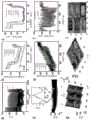
图2a至图2m所示为根据本发明实施方式的表面形貌测定方法;2a to 2m show a surface topography measurement method according to an embodiment of the present invention;
图3a至图3c所示为根据本发明实施方式对灰度强度特征以及力与Z向压电延伸曲线间关系的证明;Figures 3a-3c show demonstrations of grayscale intensity characteristics and the relationship between force and Z-direction piezoelectric extension curves according to embodiments of the present invention;
图4a至图4f所示为在本发明实施方式中利用具有24个探针针尖的探针阵列获得的结果;Figures 4a-4f show results obtained using a probe array with 24 probe tips in an embodiment of the present invention;
图5a至图5l所示为在本发明实施方式中利用91针尖并行扫描获得大区域的三维图像;Figures 5a to 5l show three-dimensional images of a large area obtained by parallel scanning of 91 needle tips in an embodiment of the present invention;
图6a和图6b所示为利用本发明实施方式测定样品表面的表面化学的方法;Figures 6a and 6b illustrate a method for determining the surface chemistry of a sample surface using an embodiment of the present invention;
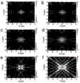
图7a至图7f所示为在本发明实施方式中通过探针针尖时域有限差分 (FDTD)仿真所产生的近场强度分布结果;Figures 7a to 7f show near-field intensity distribution results generated by a probe tip finite difference time domain (FDTD) simulation in an embodiment of the present invention;
图8为根据本发明实施方式的近场反射光强分布随距离变化图;8 is a graph showing the variation of near-field reflected light intensity distribution with distance according to an embodiment of the present invention;
图9a至图9d所示为通过变化最小Z向压电延伸,确认接触峰和分离峰的方法;Figures 9a to 9d show a method for identifying contact peaks and separation peaks by varying the minimum Z-direction piezoelectric extension;
图10a至图10f所示为以并行扫描光学显微术测量的不同尺寸的凹陷特征的原子力显微镜形貌图像;Figures 10a-10f show AFM topography images of recessed features of different sizes measured by parallel scanning optical microscopy;
图11a至图11d所示为根据本发明实施方式灰度计算中使用的探针针尖顶点周围所选面积大小对特征高度测量精度的影响;Figures 11a to 11d show the influence of the selected area size around the apex of the probe tip used in the grayscale calculation according to an embodiment of the present invention on the measurement accuracy of the feature height;
图12a至图12f所示为利用本发明实施方式区分同一基底上具有不同憎水性的微米级区域的方法。Figures 12a-12f illustrate a method for distinguishing micron-scale regions with different hydrophobicity on the same substrate using embodiments of the present invention.
具体实施方式Detailed ways
本发明实施方式提供一种新的成像技术,称为并行扫描光学显微术(ParallelScanning Optical Microscopy,PSOM)。并行扫描光学显微术融合了现有光学显微术的大面积成像优点和扫描探针显微术的高垂直分辨率。并行扫描光学显微术首次采用探针针尖顶点处的白光反射光强变化(灰度变化)作为反馈信息对表面信息进行研究,从而实现毫米级面积的同步并行扫描。Embodiments of the present invention provide a new imaging technique called Parallel Scanning Optical Microscopy (PSOM). Parallel scanning optical microscopy combines the large-area imaging advantages of existing optical microscopy with the high vertical resolution of scanning probe microscopy. For the first time, parallel scanning optical microscopy uses the reflected light intensity change (grayscale change) of the white light at the tip of the probe tip as feedback information to study surface information, thereby realizing simultaneous parallel scanning of millimeter-level areas.
除了形貌成像之外,其还可使得弹性针尖具有用于获取表面化学等的其他表面信息的功能。In addition to topography imaging, it can also enable the elastic tip to have functions for acquiring other surface information such as surface chemistry.
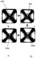
图1所示为根据本发明实施方式的并行扫描光学显微装置。如图1所示,装置100包括位于样品120上方的探针阵列110。探针阵列110包括从基底114 延伸而出的多个探针针尖112。探针针尖112由透明的可变形材料形成。在本实施方式中,所述基底由玻璃形成。探针针尖112自基底114伸向样品120的表面122。FIG. 1 shows a parallel scanning optical microscopy apparatus according to an embodiment of the present invention. As shown in FIG. 1 ,
致动器130用于移动探针阵列110,以使其接近或远离样品120的表面122,在实施方式中,致动器130为Z向压电扫描器。光源140用于向探针针尖112 提供照明光142。物镜150将来自光源140的照明光142作为入射光144引导至探针针尖112上。所述来自探针针尖的反射光146由所述物镜引导至图像捕获装置150,在本实施方式中,图像捕获装置150为相机。An
在并行扫描光学显微术(PSOM)中,采用大面积白光而非单独的小激光束对探针针尖112的整个阵列进行照明。探针阵列的面积可大至数平方毫米。这大大地扩展了现有单针尖式扫描探针显微镜的扫描面积。In parallel scanning optical microscopy (PSOM), a large area of white light is used to illuminate the entire array of
每个探针针尖112的白光反射光强变化均用作用于获取表面122的表面信息的反馈信号。The change in the reflected light intensity of the white light from each
在实施方式中,并行扫描光学显微术利用弹性体针尖112与样品的表面122 之间的物理接触对样品表面信息进行检测,从而实现形貌图像的直接获取。In an embodiment, parallel scanning optical microscopy utilizes physical contact between the
在使用中,致动器130将探针阵列110在垂直方向上移动。针对每个针尖和每个扫描点,探针阵列110均在所述垂直方向上从相同起始位置移动至相同终点位置。通过对样品的表面122进行逐点及逐行扫描,可以获得图像。In use, the
在一种实施方式中,探针针尖112由聚二甲基硅氧烷(PDMS)制成,从而实现透明的弹性体的探针针尖112。In one embodiment, the
使用入射光142为探针针尖阵列110提供背光使得探针针尖112内侧壁和样品表面产生反射光。该反射光的强度可由电荷耦合器件(CCD)相机等图像捕获装置150所拍摄的光学图像的灰度值量化。如图1所示,图像捕获装置150 设置于针尖阵列110的背面上方。当探针针尖112的顶点接触或离开样品表面 122时,来自探针针尖112的反射光强,尤其来自每个探针针尖112的顶点的反射光强会因探针针尖112的变形而大幅升高或降低。灰度的这种突然变化可用作识别探针针尖112和样品表面122之间的临界接触和分离位置的反馈信号。在与样品表面122接触之后,探针针尖112进一步移动,直至到达其具有最小Z 向压电延伸的终点位置。Backlighting the
之后,探针针尖112从样品表面122回缩,直至其返回在垂直方向上的起始位置。弹性体探针针尖112然后从所述接触位置变形至所述分离位置。由于探针针尖112的移动速度为恒速,因此对于具有不同高度的特征,探针针尖从所述临界接触位置回撤至所述临界分离位置所需的时间不同。这一时间差可用于计算特征高度,从而展现样品表面的形貌图像。由于针尖和样品表面之间的相互作用过程可能受化学力等其他力的影响,因此还可获得表面化学信息等其他表面信息。Thereafter, the
图2a至图2m所示为根据本发明实施方式的表面形貌测定的过程。图2a至图2i为探针针尖接近并接触样品表面的光学图像。Figures 2a to 2m illustrate the process of surface topography determination according to an embodiment of the present invention. Figures 2a to 2i are optical images of the probe tip approaching and contacting the sample surface.
如图2a所示,样品表面205具有平坦部分210和凹陷部分220。平坦部分 210高于凹陷部分220。第一探针针尖212位于平坦部分210上方,第二探针针尖222位于凹陷部分220上方。第一光学图像215a获得自第一探针针尖212的反射光,第二光学图像225a获得自第二探针针尖222的反射光。As shown in Figure 2a, the
如图2b所示,包含第一探针针尖212和第二探针针尖222的所述探针阵列向样品表面205移动。如图2b所示,第一探针针尖212和第二探针针尖222均不与样品表面205接触。然而,由于第一探针针尖212和第二探针针尖222更加靠近样品表面205,因此来自样品表面205的反射变得更强。图2b所示状态中的第一图像215b和第二图像225b的强度高于图2a所示状态中的第一图像 215a和第二图像225a的强度。As shown in Figure 2b, the probe array comprising the
随着所述探针阵列进一步靠近样品表面205,第一探针针尖212与样品表面 205的平坦部分210发生接触。这一状态示于图2c。As the probe array gets closer to the
如图2c所示,第一探针针尖212的顶点214与样品表面205的平坦部分210 相接触。这使得第一图像215c变暗。由于第二探针针尖222未与样品表面205 的凹陷部分220接触,因此第二图像225c仍然较为明亮。As shown in Figure 2c, the
随后,所述探针阵列进一步靠近样品表面205,从而使得第二探针针尖222 与样品表面205的凹陷部分220相接触。这一状态示于图2d。Subsequently, the probe array is brought closer to the
如图2d所示,第一探针针尖212的顶点214自其与所述样品表面的平坦部分210接触的位置发生变形。因此,第一图像215d示出了第一探针针尖212的变形。第二探针针尖222的顶点224与样品表面205的凹陷部分220接触。因此,与第二探针针尖222未与样品表面205接触时的第二图像225c相比,第二图像225d的光强发生急遽变化。As shown in Figure 2d, the
随着所述探针阵列进一步靠近样品表面205,第一探针针尖212的顶点214 进一步变形,而且第二探针针尖222的顶点224也发生变形。这一状态示于图 2e。As the probe array moves closer to the
如图2e所示,与图2d所示状态中的光强相比,第一图像215e的反射光强增大。这是因为变形后的顶点214反射了更多的光。第二探针针尖222的顶点 224虽然也发生了变形,但是其变形程度与第一探针针尖212的顶点214的变形程度不同。As shown in Figure 2e, the reflected light intensity of the
在此之后,所述探针阵列朝远离样品表面205的方向移动。After this, the probe array is moved away from the
如图2f所示,所述探针阵列在移动过程中通过了第二探针针尖222的顶点 224与样品表面205的凹陷部分220接触的位置。在该位置处,第一探针针尖 212的顶点214仍在样品表面205的平坦部分210的作用下处于变形状态。As shown in Figure 2f, the probe array passes through the location where the apex 224 of the
随着所述探针阵列进一步远离样品表面205,所述状态转变至图2g所示情形,其中,第一探针针尖212与样品表面205的平坦部分210接触,而第二探针针尖222已经脱离与样品表面205的凹陷部分220的接触的状态。如图2g所示,第一图像215g和第二图像225g对应于图2c所示第一图像215c和第二图像 225c。As the probe array moves further away from the
其后,所述探针阵列进一步远离样品表面205。如图2h所示,第一探针针尖212和第二探针针尖222均脱离与样品表面205的接触。第一图像215h和第二图像225h对应于图2b所示第一图像215b和第二图像225b。Thereafter, the probe array is moved further away from the
最后,所述探针阵列进一步远离样品表面205。如图2i所示,第一探针针尖212和第二探针针尖222均处于离样品表面205更远的位置。如图2i所示,由于样品表面205的反射更小,因此与图2h所示的第一图像215h和第二图像 225h相比,第一图像215i的光强和第二图像225i的光强均被减弱了。Finally, the probe array is further away from the
图2j为本发明实施方式的装置通过实验手段获得的灰度强度经时变化图。图2j表示了从图2a状态至图2i状态的扫描过程。由于所述探针阵列以恒定速度移动,因此可认为图2j的X轴所表示的经过时间与所述探针阵列相对于所述样品表面的位置成正比。图2j中的字母a至i表示上述图2a至图2i的状态。如上所述,所述探针阵列先朝所述样品表面移动至图2e所示状态,然后朝远离所述样品表面的方向移动。从图2j可看出,该移动方向的变化发生于所述扫描过程的约40秒钟处。FIG. 2j is a graph showing the variation of grayscale intensity with time obtained by the apparatus according to the embodiment of the present invention through experimental means. Figure 2j shows the scanning process from the state of Figure 2a to the state of Figure 2i. Since the probe array moves at a constant speed, the elapsed time represented by the X-axis of Figure 2j can be considered to be proportional to the position of the probe array relative to the sample surface. Letters a to i in Fig. 2j represent the states of Figs. 2a to 2i described above. As described above, the probe array is first moved toward the sample surface to the state shown in Figure 2e, and then moved away from the sample surface. As can be seen from Figure 2j, this change in movement direction occurs at about 40 seconds into the scanning process.
如图2j所示,所获得的灰度曲线的形状高度相似,而且由于在每一点的测量过程中所有针尖在垂直方向上均经历下述过程,因此其对于每个扫描点和每个探针针尖均可重现。在接触前,随着探针针尖接近样品表面,样品表面的反射因探针针尖离其越来越近而增大,从而使得反射光强增大。当探针针尖接触样品表面时,发生突然变化。当探针针尖接触样品表面时,反射光强突然增大,从而导致出现峰值(图2j中的峰值c和d),该峰值可用于确定临界接触位置。在接触后,随着Z向压电扫描器的进一步延伸,所述弹性体针尖发生变形,从而使得PDMS针尖表面和样品表面之间的接触面积逐渐变大,接触变强。这又导致在Z向压电延伸变为其最小值之前,光反射逐渐增强,灰度逐步增大(图 2j中的峰值e)。As shown in Fig. 2j, the shapes of the obtained grayscale curves are highly similar, and since all needle tips undergo the following process in the vertical direction during the measurement at each point, it is Needle tips are reproducible. Before contact, as the probe tip approaches the sample surface, the reflection from the sample surface increases as the probe tip gets closer to it, thereby increasing the reflected light intensity. A sudden change occurs when the probe tip touches the sample surface. When the probe tip contacts the sample surface, the reflected light intensity suddenly increases, resulting in a peak (peaks c and d in Figure 2j) that can be used to determine the critical contact location. After the contact, with the further extension of the piezoelectric scanner in the Z direction, the elastomer tip is deformed, so that the contact area between the PDMS tip surface and the sample surface is gradually enlarged, and the contact becomes stronger. This in turn results in a gradual increase in light reflection and a gradual increase in gray scale before the piezoelectric extension in the Z direction reaches its minimum value (peak e in Fig. 2j).
图2k至图2n为本发明实施方式中CCD相机所捕获的其中一个被选探针针尖的背面图像。图2k为当探针针尖未与样品表面接触时所捕获的图像。该探针针尖的顶点区域230k已在图中圈出。图2l为探针针尖与样品表面刚接触时所捕获的图像。在下文中,该状态称为“临界接触”状态。如图2l所示,该图像中的顶点区域230l因探针针尖与样品表面的接触而更暗。图2m为探针针尖因与样品表面接触而发生变形后所捕获的图像。如图2m所示,该图像的顶点区域230m 因探针针尖的变形而变得更亮。图2n为当探针针尖脱离与样品表面的接触时所捕获的图像。在下文中,该状态称为“临界分离”状态。如图2n所示,该图像的顶点区域230n变得更暗。如上所述,当探针针尖与样品表面发生接触时,以及当探针针尖脱离与样品表面的接触时,所述光强发生变化。在本发明实施方式中,当所述探针阵列朝接近和/或远离样品表面的方向移动时,对所述阵列中的每个探针针尖的强度变化进行检测。如此,便可根据所测光强变化的时间点,确定样品表面形貌信息。Figures 2k to 2n are rear images of one of the selected probe tips captured by the CCD camera in the embodiment of the present invention. Figure 2k is an image captured when the probe tip is not in contact with the sample surface. The
如上所述,当所述Z向扫描器已经获得图2e所示状态中的最小Z向压电延伸时,将已变形的探针针尖相对于所述样品表面回撤。由于探针针尖在接近样品表面以及从样品表面处回撤过程中所做的运动可逆,上述灰度/时间曲线为对称曲线。正如图2j所示,回撤过程的曲线部分(图2j的曲线段e-i)与接近过程的曲线部分(曲线段a-e)相反。As described above, the deformed probe tip is retracted relative to the sample surface when the Z-scanner has achieved the minimum Z-piezoelectric extension in the state shown in Figure 2e. Since the motion of the probe tip in approaching and retracting from the sample surface is reversible, the above grayscale/time curve is a symmetric curve. As shown in Fig. 2j, the curve portion of the pullback process (curve segment e-i of Fig. 2j) is opposite to the curve portion of the approach process (curve segment a-e).
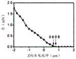
图3a至图3c所示为对所述灰度强度特征与力/Z向压电延伸曲线间关系的证明。Figures 3a to 3c show demonstrations of the relationship between the grayscale intensity characteristics and the force/Z-direction piezoelectric extension curve.
图3a为实验装置示意图。如图3a所示,探针阵列310置于作为样品320 的硅片上方。硅片样品320置于数字量计325之上,该数字量计用于测量由探针阵列310施加于样品320上的力,以及测定探针阵列310自样品320分离的时间点。Figure 3a is a schematic diagram of the experimental setup. As shown in Figure 3a, the
如图3a所示,当探针阵列310与样品320接触时,所述数字量计的读数为正。数字量计325的读数为零之时为所述分离开始时的时间点。As shown in Figure 3a, when the
图3b所示为数字量计325所测的力与Z向压电延伸距离之间的关系。从图 3b可看出,当所述延伸距离介于0.6μm和0.8μm之间时,所述力变为0。Figure 3b shows the relationship between the force measured by the
图3c所示为与所述探针阵列的其中一个被选探针针尖对应的图像捕获装置的灰度读数。如图3c所示,0.7μm处出现一个清晰的峰。Figure 3c shows a grayscale reading of the image capture device corresponding to one of the selected probe tips of the probe array. As shown in Fig. 3c, a clear peak appeared at 0.7 μm.
如上所述,在针尖阵列回撤过程中可发现,当Z向压电延伸从0.6μm增大至0.8μm时,针尖阵列与样品表面之间的力从0.05mN变为0mN。从图3b可看出,所述临界分离位置在垂直方向上的Z向压电延伸原理上应处于0.6~0.8μm 范围。如图3c所示,通过利用上述方法的灰度/Z向压电延伸曲线,可发现所述分离峰处于Z向压电延伸为0.7μm时的垂直位置。由于从灰度曲线获得的0.7μm 的Z向压电延伸落入上述范围,因此可以证明从所述灰度曲线看到的峰(图2j 的峰f和g)为分离峰。由于所述接触过程与分离过程为可逆过程,因此所述接触峰位置也获得证明。As described above, during retraction of the tip array, it can be found that the force between the tip array and the sample surface changes from 0.05 mN to 0 mN as the Z-direction piezoelectric extension increases from 0.6 μm to 0.8 μm. It can be seen from Fig. 3b that the Z-direction piezoelectric extension in the vertical direction of the critical separation position should be in the range of 0.6-0.8 μm in principle. As shown in Figure 3c, by using the grayscale/Z-direction piezoelectric extension curve using the above method, it can be found that the separation peak is at a vertical position when the Z-direction piezoelectric extension is 0.7 μm. Since the Z-direction piezoelectric extension of 0.7 μm obtained from the grayscale curve falls within the above range, it can be proved that the peaks seen from the grayscale curve (peaks f and g of FIG. 2j ) are separated peaks. Since the contact process and separation process are reversible processes, the contact peak positions are also confirmed.
将并行扫描光学显微术与传统扫描探针显微术相互区分开来的一项独特特征为由数百个探针针尖组成的所述探针阵列带来的高通量成像能力,由于所有探针针尖均具有由所述相机收集的相应光学图像且均参与成像,从而实现了高通量成像能力。A unique feature that distinguishes parallel scanning optical microscopy from traditional scanning probe microscopy is the high-throughput imaging capability brought about by the probe array, consisting of hundreds of probe tips, due to all the The probe tips all have corresponding optical images collected by the camera and all participate in imaging, thereby achieving high-throughput imaging capabilities.
图4a至图4f所示为在本发明实施方式中利用具有24个探针针尖的探针阵列所获得的结果。作为概念验证,选择针尖阵列当中的5个针尖作为屏幕上24 个针尖的代表,展示其所实施的亚衍射特征高度并行同步测量方法。图4a所示为显示所述24个探针针尖当中每个针尖的图像415的屏幕。图4b所示为所述探针阵列中的5个所选探针针尖从相继实施的8次测量当中的第1次测量的开始时间起的灰度强度与时间关系。每次测量均涉及将所述探针阵列的探针针尖移动至与所述样品表面接触,然后再将其移动至与所述样品表面脱离接触。在前四次测量中,所述探针阵列与所述样品表面的相同平坦部分相接触。之后,在后四次测量中,所述探针阵列与所述样品表面的凹陷部分相接触。Figures 4a-4f show the results obtained using a probe array with 24 probe tips in an embodiment of the present invention. As a proof-of-concept, 5 tips in the tip array were chosen to represent the 24 tips on the screen, demonstrating the highly parallel simultaneous measurement of sub-diffractive features implemented. Figure 4a shows a screen showing an
图4c所示为针对每个所选探针针尖在各次测量实验中的从接触到分离的时间。如图4c所示,在前四次测量实验中,每个所述探针针尖的接触和分离之间的时间为40~42秒。在后四次测量实验中,接触和分离之间的时间为34~36秒。可见,与所述凹陷处相比,所选5个针尖在所述平坦处从接触位置过渡到分离位置所需的时间要长的多。Figure 4c shows the time from contact to separation in each measurement experiment for each selected probe tip. As shown in Figure 4c, in the first four measurement experiments, the time between the contact and separation of each of the probe tips was 40-42 seconds. In the last four measurement experiments, the time between contact and separation was 34-36 seconds. It can be seen that the time required for the transition of the selected 5 needle tips from the contact position to the separation position is much longer at the flat position compared to the depression position.
在第一种特征高度计算方法中,其使用接触和分离之间的时间差。在第二种特征高度计算方法中,其使用针尖在上述两处从起始位置过渡至临界接触位置所花费的时间差。In the first feature height calculation method, it uses the time difference between contact and separation. In the second feature height calculation method, it uses the time difference it takes for the tip to transition from the initial position to the critical contact position at the above two points.
图4d所示为针对所述5个所选探针针尖当中的每个针尖通过不同方法所计算出的特征高度与实际高度(260nm)之间的比较结果。如图4d所示,所计算出的特征高度与实际特征高度间的误差处于60nm范围内。Figure 4d shows the comparison results between the calculated feature height and the actual height (260 nm) by different methods for each of the 5 selected probe tips. As shown in Figure 4d, the error between the calculated feature height and the actual feature height is in the range of 60 nm.
图4e所示为3个所选探针针尖对55nm高的特征进行测量时的高度测量值。如图4e所示,高度测量值与实际特征高度之间的误差处于15nm范围内。Figure 4e shows the height measurements for 55nm-tall features with three selected probe tips. As shown in Fig. 4e, the error between the height measurement and the actual feature height is in the range of 15 nm.
图4f所示为4个所选探针针尖对35nm高的特征进行测量时的高度测量值。如图4f所示,该4个探针针尖的平均测量值为36nm左右。Figure 4f shows height measurements for 35nm-tall features with 4 selected probe tips. As shown in Fig. 4f, the average measured value of the four probe tips was around 36 nm.
如以上参考图4e和图4f所示,利用此方法对高度为55nm和30nm的特征进行测量时的误差分别为30nm和18nm。如图4b所示,在每次测量实验当中,每个针尖的灰度均有规律地进行变化,证明了上述灰度与时间曲线的可重现性。As shown above with reference to Figures 4e and 4f, the errors when measuring features with heights of 55 nm and 30 nm using this method are 30 nm and 18 nm, respectively. As shown in Figure 4b, in each measurement experiment, the gray scale of each needle tip changes regularly, which proves the reproducibility of the above gray scale and time curve.
图5a至图5l所示为利用91个针尖对较大面积进行并行扫描时所获得的三维图像。通过对各个特征进行沿直线的逐点式扫描,可获得这些特征的线轮廓。Figures 5a to 5l show 3D images obtained when 91 tips were used to scan a large area in parallel. The line profile of each feature is obtained by performing a point-by-point scan of each feature along a straight line.
图5a所示为6个探针针尖的灰度强度与帧数的关系图。图5b所示为接触峰与分离峰之间的帧数计算值与扫描距离之间的关系。如图5b所示,在每个扫描点处,可针对每个针尖计算临界接触位置与临界分离位置之间的帧数。如图 5c所示,平坦处与深度为260nm的40μm×40μm方孔处之间的上述帧数差可用于计算该特征高度。Figure 5a shows the relationship between the grayscale intensity of the six probe tips and the number of frames. Figure 5b shows the relationship between the calculated number of frames between the contact peak and the separation peak and the scan distance. As shown in Figure 5b, at each scan point, the number of frames between the critical contact position and the critical separation position can be calculated for each tip. As shown in Figure 5c, the above frame number difference between the flat and the 40 μm × 40 μm square hole with a depth of 260 nm can be used to calculate this feature height.
在扫描过程中,虽然采用压电扫描器闭环降低热漂移,但是Z向压电扫描器的热漂移仍然是一个不可避免的问题,从而导致不同扫描点的灰度曲线背景中产生斜度。这些斜度即图5a中的灰度强度的逐渐变化,而且在图5b以直线 510标出。与原子力显微镜图像处理中广泛采用的做法一致,热漂移导致的误差可通过曲线平滑法进行校正。During the scanning process, although the closed-loop piezoelectric scanner is used to reduce thermal drift, the thermal drift of the Z-direction piezoelectric scanner is still an unavoidable problem, which leads to a slope in the background of the grayscale curve at different scanning points. These slopes are the gradual changes in grayscale intensity in Figure 5a, and are marked by
通过对原始曲线进行线性拟合,可以获得背景直线。在将该背景直线从原始曲线中减去后,可降低Z向压电扫描器热漂移所导致的斜度,并获得图5c所示的特征形貌轮廓线。对于所有的6个所选针尖,所述方形特征的高度和宽度测量值均分别接近于其260nm的实际高度与40μm的实际宽度。The background straight line can be obtained by linearly fitting the original curve. After subtracting this background line from the original curve, the slope due to thermal drift of the piezo scanner in the Z-direction can be reduced and the characteristic topography profile shown in Figure 5c is obtained. For all 6 selected tips, the square feature's height and width measurements were close to its actual height of 260 nm and actual width of 40 μm, respectively.
在通过逐点扫描获得上述线轮廓之后,再利用所述针尖阵列以逐行方式对样品表面区域进行扫描,便可获得3D形貌图像。之后,通过将各个针尖的扫描区域进行缝合,便可获得大面积图像。图5d至图5i所示为以所述阵列的每个探针针尖对60μm×60μm区域进行32点×32点扫描时的结果。After the above-mentioned line profile is obtained by point-by-point scanning, the surface area of the sample is scanned row by row by using the needle tip array to obtain a 3D topographic image. Afterwards, large-area images can be obtained by stitching the scanned area of each needle tip. Figures 5d to 5i show the results of scanning a 60 μm×60 μm area with 32×32 points with each probe tip of the array.
图5d所示为所述探针针尖当中的一个在一次试验过程中的灰度与帧数的曲线。其中的插图为从主图中选出的一次实验过程的灰度和帧数的曲线。Figure 5d shows a graph of the grayscale versus frame number of one of the probe tips during a test. The inset is the curve of grayscale and frame number of an experimental process selected from the main image.
图5e为所选6个探针针尖当中的每个针尖的接触峰与分离峰之间的帧数计算值与实验次数之间的关系图。FIG. 5e is a graph showing the relationship between the calculated value of the number of frames between the contact peak and the separation peak of each of the selected six probe tips and the number of experiments.
图5f为从图5e所示数据得出的两个所选探针针尖的特征高度计算值与实验次数的关系图。Figure 5f is a graph of calculated characteristic heights of two selected probe tips versus the number of experiments derived from the data shown in Figure 5e.
图5g为一个120μm×180μm所选区域的3D形貌图像。图5g所示数据得自 6个并行扫描的探针针尖,并由matlab程序绘制。Figure 5g is a 3D topography image of a selected area of 120 μm × 180 μm. The data shown in Figure 5g were obtained from 6 probe tips scanned in parallel and plotted by a matlab program.
图5h为对图5g所示3D形貌图像进行平滑处理后的图像。Figure 5h is an image after smoothing the 3D topography image shown in Figure 5g.
图5i为与图5g和图5h所示3D形貌图像对应的2D形貌图像。Figure 5i is a 2D topography image corresponding to the 3D topography images shown in Figures 5g and 5h.
图5j至图5l所示为以所述针尖阵列中的每个探针针尖对40μm×40μm区域内的相隔10μm的高度为180nm且宽度为30μm方形凹陷特征进行32像素×32 像素扫描的方法。所述PDMS探针针尖分别具有30μm的背面长度及10μm的间隔。Figures 5j to 5l illustrate a method of scanning 32 pixels by 32 pixels of square recessed features with a height of 180 nm and a width of 30 μm within a 40 μm×40 μm area with each probe tip in the tip array. The PDMS probe tips had a backside length of 30 μm and a spacing of 10 μm, respectively.
图5j为高速相机所所捕获的91探针针尖并行成像的光学图像520当中的一幅。其中的插图部分530所示为两个相邻的探针针尖。Figure 5j is one of the 91 parallel-imaging
图5k为以91个探针针尖对0.15mm2区域进行并行扫描时获得的3D形貌图像。Figure 5k is a 3D topography image obtained when a0.15mm2 area was scanned in parallel with 91 probe tips.
图5l为选自图5k所示的3D形貌图像的120μm×80μm区域的3D形貌图像。Figure 5l is a 3D topography image selected from a 120 μm x 80 μm area of the 3D topography image shown in Figure 5k.
作为概念验证,所述探针针尖阵列用于对具有不同特征高度(如以上参照图5d~图5i所述的260nm,以及参照图5j~图5l所述的180nm)的表面特征进行扫描。所获得的形貌图像与实际表面形貌具有良好的一致性,而且该方法所测量的特征尺寸也接近实际的特征尺寸。所述形貌图像中引入的热漂移可通过实施与如图5e至图5h一样的图像平滑处理得到校正。As a proof of concept, the probe tip array was used to scan surface features with different feature heights (eg 260 nm as described above with reference to Figures 5d-5i, and 180 nm as described with reference to Figures 5j-5l). The obtained topography images are in good agreement with the actual surface topography, and the feature size measured by this method is also close to the actual feature size. The thermal drift introduced in the topography image can be corrected by performing image smoothing as in Figures 5e to 5h.
具体而言,利用91针尖的并行扫描可在一次实验中获得0.28mm×0.52mm 区域的3D形貌图像,从而将现有单针尖式的原子力显微镜(80μm×80μm X-Y 扫描器)的扫描面积拓展23个数量级。并行扫描光学显微术的大面积成像可能适用于在大面积样品表面上对感兴趣的部位进行搜索。Specifically, a 3D topography image of a 0.28mm×0.52mm area can be obtained in one experiment using the parallel scanning of the 91-tip, thus expanding the scanning area of the existing single-tip type atomic force microscope (80μm×80μm X-Y scanner). 23 orders of magnitude. Large-area imaging with parallel scanning optical microscopy may be suitable for searching for sites of interest on large-area sample surfaces.
在本发明实施方式中,所述探针针尖阵列还可用于检测化学力,从而区分亲水性表面和疏水性表面等具有不同憎水性的表面。In an embodiment of the present invention, the probe tip array can also be used to detect chemical forces, so as to distinguish surfaces with different hydrophobicity, such as hydrophilic surfaces and hydrophobic surfaces.
在一种实施方式的表现形式中,采用带有-NH2基团的3-氨基丙基三乙氧基硅烷(APTES)以及带-CH3基团的十八烷基三甲氧基硅烷(OTMS)对硅表面进行改性,以使其分别成为亲水性和疏水性的表面。In one embodiment, 3-aminopropyltriethoxysilane (APTES) with -NH2 group and octadecyltrimethoxysilane (OTMS) with -CH3 group are used to The silicon surface is modified to make it hydrophilic and hydrophobic, respectively.
图6a所示为涂有相同的PDMS的氮化硅针尖与分别通过亲水性–NH2基团和疏水性–CH3基团改性的硅表面之间的代表性力与拔出距离的关系曲线。Figure 6a shows representative force versus pull-out distance between a silicon nitride tip coated with the same PDMS and a silicon surface modified by hydrophilic –NH2 groups and hydrophobic –CH3 groups, respectively. .
图6b所示为6次重复实验中所选的6个针尖分别通过以–NH2基团改性的亲水性表面和以–CH3基团官能化的疏水性表面所获得的平均Z向延伸差。Figure 6b shows the average Z-direction extension difference obtained by the hydrophilic surface modified with –NH2 groups and the hydrophobic surface functionalized with –CH3 groups for 6 tips selected in 6 replicates, respectively. .
通过–NH2和–CH3改性的硅表面的接触角测量值分别为51°和100°。为了研究PDMS针尖与具有不同憎水性的样品表面之间的相对化学作用,在原子力显微镜中采用一种经同样的氧等离子体处理的涂有PDMS的氮化硅针尖,并使其接触上述两种样品表面,以获得如图6a所示的环境空气中拔出力曲线。结果表明,亲水性表面的拔出力大于疏水性表面的拔出力,这表明涂有PDMS的亲水性针尖与亲水性表面之间的相互作用更强。其原因可能在于,正如化学力显微术中的先前研究结果所述的两个亲水性表面之间的弯月面力大于亲水性表面和疏水性表面之间的弯月面力。The contact angle measurements of the silicon surfaces modified by –NH2 and –CH3 are 51° and 100°, respectively. To study the relative chemistry between the PDMS tip and sample surfaces with different hydrophobicity, an identical oxygen plasma treated silicon nitride tip coated with PDMS was used in atomic force microscopy and brought into contact with the two sample surface to obtain the pull-out force curve in ambient air as shown in Figure 6a. The results show that the pull-out force of the hydrophilic surface is greater than that of the hydrophobic surface, which indicates that the interaction between the hydrophilic tip coated with PDMS and the hydrophilic surface is stronger. The reason for this may be that the meniscus force between the two hydrophilic surfaces is greater than the meniscus force between the hydrophilic and hydrophobic surfaces, as described in previous findings in chemical force microscopy.
在本发明实施方式中,在同一次实验当中,临界分离位置处的Z向压电延伸大于临界接触位置处的Z向压电延伸,这是因为在分离过程中PDMS针尖与硅表面之间的化学相互作用对该弹性体针尖具有拖拽作用,而在接触过程不具有该作用。In the embodiment of the present invention, in the same experiment, the Z-direction piezoelectric extension at the critical separation position is greater than the Z-direction piezoelectric extension at the critical contact position because of the separation between the PDMS tip and the silicon surface during the separation process. Chemical interactions have a drag on the elastomer tip, but not during contact.
本文中,将上述接触位置与所述分离位置之间的Z向延伸值之差定义为Z 向延伸差,其可用于区分亲水性表面和疏水性表面。原则上,由于亲水性表面的拔出力大于疏水性表面的拔出力,因此亲水性表面的Z向延伸差大于疏水性表面的Z向延伸差。Herein, the difference in the Z-direction extension value between the above-mentioned contact position and the separation position is defined as the Z-direction extension difference, which can be used to distinguish between hydrophilic and hydrophobic surfaces. In principle, since the pull-out force of a hydrophilic surface is greater than that of a hydrophobic surface, the difference in Z-direction extension of a hydrophilic surface is greater than that of a hydrophobic surface.
如图6b所示,对于所选的6个针尖中的所有针尖,所获得的实验结果与预测结果具有良好的一致性,这表明基于化学的该并行扫描光学显微术可用于区分具有不同憎水性的表面。As shown in Fig. 6b, the obtained experimental results are in good agreement with the predicted results for all of the selected 6 tips, suggesting that this chemical-based parallel scanning optical microscopy can be used to differentiate water-based surface.
以下将对本发明实施方式的制造及使用进行说明。The manufacture and use of embodiments of the present invention will be described below.
所述聚合物针尖通过先对硅(100)进行常规光刻,然后对其进行各向异性湿法刻蚀的方法制成。首先,在具有280nm厚的二氧化硅层的硅片上旋涂 Shipley1805(MicroChem公司)光刻胶,然后利用SUSS公司(德国加兴)的MJB4光刻机进行光刻,以形成网格图案。之后,将曝光后的方形二氧化硅图案在市售的缓冲氢氟酸(Transene Company公司)中刻蚀4分钟,以去除未受保护的二氧化硅。其后,将该基底放入80℃的湿法刻蚀溶液(通过将质量百分比为35%的氢氧化钾溶液加入水:异丙醇体积比为4:1的溶液制成)中,以在充分搅拌条件下对曝光后的硅进行各向异性刻蚀,从而形成内陷的金字塔形图案。剩余的二氧化硅层通过在缓冲氢氟酸(Transene Company公司)内进行的湿法刻蚀去除。随后,先将模具在90℃的食人鱼溶液(硫酸/双氧水(70/30))中浸泡15分钟,以使其具有亲水性,然后通过气相硅烷化,以1H,1H,2H,2H-全氟十二烷基三氯硅烷(Gelest公司)对所述硅母料进行改性,以防止发生粘附。The polymer tip is fabricated by conventional photolithography of silicon (100) followed by anisotropic wet etching. First, Shipley 1805 (MicroChem) photoresist was spin-coated on a silicon wafer with a 280 nm-thick silicon dioxide layer, and then photolithography was performed using an MJB4 lithography machine from SUSS (Gaching, Germany) to form a grid pattern. Afterwards, the exposed square silicon dioxide pattern was etched in commercially available buffered hydrofluoric acid (Transene Company) for 4 minutes to remove unprotected silicon dioxide. Thereafter, the substrate was put into a wet etching solution at 80° C. (made by adding a 35% by mass potassium hydroxide solution to a solution with a water:isopropanol volume ratio of 4:1) to The exposed silicon is anisotropically etched under well-stirred conditions to form indented pyramidal patterns. The remaining silicon dioxide layer was removed by wet etching in buffered hydrofluoric acid (Transene Company). Subsequently, the mold was first immersed in a piranha solution (sulfuric acid/hydrogen peroxide (70/30)) at 90°C for 15 minutes to make it hydrophilic, and then by gas phase silanization, with 1H, 1H, 2H, 2H- The silicon masterbatch was modified by perfluorododecyltrichlorosilane (Gelest) to prevent sticking.
所述聚合物探针阵列由硬PDMS(h-PDMS)制成。首先,将富含乙烯基化合物的预聚物(VDT-731,Gelest公司)与质量比为20ppm的铂催化剂(铂/二乙烯四甲基二硅氧烷络合物的二甲苯溶液,SIP6831.1,Gelest公司)及质量比为0.1%的调节剂(2,4,6,8-四甲基四乙烯基环四硅氧烷,Fluka公司)相混合。然后,将如此获得的富含乙烯基化合物的预聚物(VDT-731,Gelest公司)再与富含含氢硅烷的交联剂(HMS-301)以3:1(质量比)的比例相混合。在混合和真空脱气后,将所述混合物倾倒于所述硅母料之上。随后,将预先清洁的玻璃片(VWR公司)置于所述混合物之上。在将该弹性体混合物在80℃下过夜固化后,再将其从所述硅母料上剥下,以用于成像应用。The polymer probe array is made of hard PDMS (h-PDMS). First, a vinyl-rich prepolymer (VDT-731, Gelest Corporation) was mixed with a platinum catalyst (platinum/divinyltetramethyldisiloxane complex in xylene solution, SIP6831) with a mass ratio of 20 ppm. 1, Gelest Company) and a regulator (2,4,6,8-tetramethyltetravinylcyclotetrasiloxane, Fluka Company) with a mass ratio of 0.1%. Then, the thus-obtained vinyl compound-rich prepolymer (VDT-731, Gelest) was mixed with a hydrosilane-rich crosslinking agent (HMS-301) in a ratio of 3:1 (mass ratio). mix. After mixing and vacuum degassing, the mixture was poured over the silicon masterbatch. Subsequently, a pre-cleaned glass sheet (VWR Corporation) was placed on top of the mixture. After curing the elastomeric mixture at 80°C overnight, it was peeled from the silicone masterbatch for imaging applications.
在本实施例中,1cm×1cm的聚合物针尖阵列(从平坦的聚合物基底延伸而出的大约15000个聚二甲基硅氧烷(PDMS)针尖)被用于基于Park扫描探针平版印刷系统的并行扫描光学显微术中。虽然本实施例中的扫描探针显微系统采用压电扫描器实现针尖的纳米级精度的三维移动,但是并行扫描光学显微术并不一定需要扫描探针显微平台。具有两种不同尺寸及周期排列方式的探针针尖用于成像。一种探针针尖的边长为40μm,相邻针尖之间的间距为40μm;另一种探针针尖的边长为30μm,相邻针尖之间的间距为10μm。In this example, a 1 cm x 1 cm array of polymer tips (approximately 15,000 polydimethylsiloxane (PDMS) tips extending from a flat polymer substrate) was used for Park-based scanning probe lithography System in Parallel Scanning Optical Microscopy. Although the scanning probe microscopy system in this embodiment uses a piezoelectric scanner to realize the three-dimensional movement of the needle tip with nanoscale precision, the parallel scanning optical microscopy does not necessarily require a scanning probe microscopy stage. Probe tips with two different sizes and periodic arrangements are used for imaging. One probe tip has a side length of 40 μm, and the distance between adjacent needle tips is 40 μm; the other probe needle tip has a side length of 30 μm, and the distance between adjacent needle tips is 10 μm.
所述探针针尖阵列支承于刚性透明玻璃片上。压电扫描器(用于使该针尖阵列穿过指定区域)偏离所述玻璃片设置,以防止因对光形成阻挡而使得其不能通过所述玻璃片和针尖阵列。所述透明玻璃片还进一步粘附至金属网架上。该金属网架与所述玻璃片的边缘粘贴,以免对透射所述针尖阵列的光形成阻挡。所述金属网架进一步固定于Z向(即垂向)压电扫描器(控制所述针尖阵列的垂向运动)上。成像前,先通过设于所述针尖阵列背面上方的光学显微镜以光学方式将该针尖阵列相对于所述基底的表面调平,以确保该针尖阵列平面平行于所述样品表面平面。当针尖对所述表面进行扫描时,Z向压电提升速度和延伸速度设定为相同的常数。在特征高度的点测量过程中,Z向压电提升速度和延伸速度设定为100nm/s,而垂直方向的Z向压电延伸从2μm变化至-2μm。为了获取线和区域的形貌图像时,垂直方向的Z向压电延伸以1μm/s的速度从1.4μm 变化至-1.4μm。所述XY平台的移动速度固定于100μm/s。所述用于对针尖阵列进行照明的光源为白光发光二极管。只要光在成像过程中相对于装置的其他部分处于固定位置,则所述光源的位置并不重要。我们将每个针尖在接触前后的反射光强变化用作用于计算特征高度及探究表面形貌的信号。因此,绝对反射光强并不重要,重要的仅是所述反射光强的变化。所述光源的位置可能对不同探针针尖上的光强均匀性具有影响。然而,只要用于每个针尖的入射光强在接触前后不发生变化,那么即使针尖阵列上的入射光强不均匀,其也不会对特征高度的计算造成影响。The probe tip array is supported on a rigid transparent glass sheet. Piezoelectric scanners (for passing the array of tips through a designated area) are positioned offset from the glass sheet to prevent light from being blocked from passing through the glass sheet and the array of tips. The transparent glass sheet is further adhered to the metal mesh frame. The metal mesh frame is pasted with the edge of the glass sheet to avoid blocking the light transmitted through the needle tip array. The metal grid is further fixed on the Z-direction (ie vertical) piezoelectric scanner (which controls the vertical movement of the needle tip array). Prior to imaging, the tip array was optically leveled relative to the surface of the substrate by an optical microscope positioned above the back of the tip array to ensure that the tip array plane was parallel to the sample surface plane. As the needle tip scans the surface, the Z-direction piezo lift and extension speeds are set to the same constant. During the point measurement of the feature height, the Z-direction piezo lift speed and extension speed were set to 100 nm/s, while the Z-direction piezo-extension in the vertical direction was varied from 2 μm to −2 μm. The Z-direction piezoelectric extension in the vertical direction was varied from 1.4 μm to −1.4 μm at a rate of 1 μm/s in order to obtain topographic images of lines and regions. The moving speed of the XY stage was fixed at 100 μm/s. The light source used for illuminating the needle tip array is a white light emitting diode. The position of the light source is not important as long as the light is in a fixed position relative to the rest of the device during imaging. We used the change in reflected light intensity for each tip before and after contact as a signal for calculating feature heights and exploring surface topography. Therefore, the absolute reflected light intensity is not important, only the change in said reflected light intensity is important. The location of the light source may have an effect on the uniformity of light intensity across different probe tips. However, as long as the incident light intensity for each tip does not change before and after contact, even if the incident light intensity is not uniform across the tip array, it will not affect the calculation of the feature height.
本发明中,采用两种方法计算特征高度。由于采用同一Z向压电扫描器同步移动所有探针针尖,因此所有探针针尖的移动速度(ν)可预先确定为相同的常数。在获取图像的过程中,所有实验中的所有针尖均自垂直方向上的同一起始位置移动至垂直方向上的同一终点位置。In the present invention, two methods are used to calculate the feature height. Since the same Z-direction piezoelectric scanner is used to move all probe tips synchronously, the moving speed (ν) of all probe tips can be predetermined to be the same constant. During image acquisition, all needle tips in all experiments were moved from the same starting position in the vertical direction to the same end position in the vertical direction.
假设图2a至图2 i中的第一探针针尖212和第二探针针尖222具有相同的高度,由于第一探针针尖212从图2a所示的起始位置移动至图2c所示的平坦处 210的接触位置的垂向行程小于第二探针针尖222从图2a所示的相同起始位置移动至图2d所示的凹陷处220的接触位置的垂向行程,因此第一探针针尖212 从图2a所示的位置移动至图2c所示的位置所需的时间tac短于第二探针针尖222 从图2a所示的位置移动至图2d所示的位置所需的时间tad。凹陷特征220相对于平坦处210的相对高度可通过将tac和tad的时间差乘以所述探针阵列的移动速度的方式算出,此即为特征高度计算方法1。Assuming that the
D=(tad-tac)×ν (1)D=(tad -tac )×ν (1)
在探针针尖接触样品表面(图2c所示的第一探针针尖212的位置)后,随着Z向压电扫描器的进一步延伸,该弹性针尖一直处于变形状态,直至其在回撤过程中与样品表面分离(图2g所示的第一探针针尖212位置)。第一探针针尖212从图2c所示的接触位置至图2g所示的平坦处210的分离位置的垂向行程(dcg)大于第二探针针尖222从图2d所示的凹陷处220的接触位置至图2f 所示的分离位置的行程(ddf)。由于所述探针针尖经历了延伸和回撤两个过程,因此dcg和ddf之间的行程差应为特征高度的两倍。所述凹陷特征相对于所述平坦处的相对高度可通过将tcg与tdf间的时间差的一半乘以针尖移动速度的方式算出,此即为特征高度计算方法2。After the probe tip contacts the sample surface (the position of the
D=1/2×(tcg-tdf)×ν (2)D=1/2×(tcg -tdf )×ν (2)
在图2中,第一探针针尖212和第二探针针尖222也可视为同一针尖分别在样品表面平坦处和凹陷处扫描时所经历的两个不同位置。如此,上述方法1 和方法2均可用于计算特征高度。在计算出不同扫描点处的相对特征高度之后,扫描区域的形貌图像便可呈现。In FIG. 2 , the
所述探针针尖的光学图像由设于所述针尖阵列背面上方的高速彩色相机 (型号:acA 2040-180kc)捕获。该高速相机以187帧/秒的最大速度及2046像素×2046像素的最大分辨率捕获图像。该高速相机对应于上述扫描速度。优选地,高速相机用于高速测量,而低速相机相应用于较低的扫描速度。成像过程中的针尖光学图像由StreamPix 6软件录制为视频。在上述实验中,选择每个针尖顶点附近3像素×3像素的固定区域用于光学图像灰度分析。来自针尖顶点的反射光位于针尖的背面光学图像的中心。Optical images of the probe tips were captured by a high-speed color camera (model: acA 2040-180kc) positioned over the back of the tip array. The high-speed camera captures images at a maximum speed of 187 frames per second and a maximum resolution of 2046 pixels by 2046 pixels. This high-speed camera corresponds to the above-mentioned scanning speed. Preferably, high-speed cameras are used for high-speed measurements, while low-speed cameras are correspondingly used for lower scanning speeds. Optical images of the tip during imaging were recorded as videos by
所有的图像和数据都通过一个自制matlab程序进行分析。举例而言,通过自制的matlab程序对所述视频进行分析,以针对该视频中的每一帧获得选定区域的平均灰度值。在获得灰度相对于帧的曲线后,可利用所述matlab程序通过峰值位置识别出临界接触位置和临界分离位置的帧数。由于所述高速相机以恒速捕获图像,因此可计算出每个扫描点处从接触位置到分离位置所经历的时间,该时间可用于计算特征高度。随后,可利用matlab程序呈现各特征的线轮廓以及3D形貌图像。其中,在识别所述接触和分离位置之前,使用百分位数过滤法对所述灰度曲线进行平滑处理。All images and data were analyzed by a self-made matlab program. For example, the video is analyzed by a self-made matlab program to obtain the average gray value of the selected area for each frame in the video. After the grayscale versus frame curve is obtained, the matlab program can be used to identify the frame numbers of the critical contact position and the critical separation position through the peak position. Since the high-speed camera captures images at a constant speed, the time elapsed from the contact position to the separation position at each scan point can be calculated, which can be used to calculate the feature height. Then, the line profile and 3D topography image of each feature can be presented using the matlab program. Wherein, before identifying the contact and separation positions, a percentile filtering method is used to smooth the grayscale curve.
为了研究针尖和硅片基板交界处的场增强演进图案,使用时域有限差分 (FDTD)仿真法获得针尖阵列的法线入射光的光线跟踪仿真。In order to study the field enhancement evolution pattern at the interface of the tip and the silicon substrate, a ray-tracing simulation of the normal incident light of the tip array was obtained using finite difference time domain (FDTD) simulation method.
图7a至图7e所示为FDTD仿真所生成的近场强度仿真结果。图7a所示为 Z向压电延伸为0nm时的结果,图7b所示为Z向压电延伸为-28nm时的结果,图7c所示为Z向压电延伸为-128nm时的结果,图7d所示为Z向压电延伸为 -228nm时的结果,图7e所示为Z向压电延伸为-828nm时的结果,图7f所示为 Z向压电延伸为-1828nm时的结果。为了清楚起见,仅示出了大小为6μm×6μm 的中心区域。Figures 7a to 7e show the near-field strength simulation results generated by the FDTD simulation. Figure 7a shows the results when the Z-direction piezoelectric extension is 0 nm, Figure 7b shows the results when the Z-direction piezoelectric extension is -28 nm, and Figure 7c shows the results when the Z-direction piezoelectric extension is -128 nm, Figure 7d shows the results at a Z-direction piezoelectric extension of -228 nm, Figure 7e shows the Z-direction piezoelectric extension at -828 nm, and Figure 7f shows the results at a Z-direction piezoelectric extension of -1828 nm . For clarity, only the central region with a size of 6 μm × 6 μm is shown.
上述FDTD仿真由商业软件包(Lumerical FDTD solution v.8.6.3)实施。所采用的硅的折射率来自实验数据。所使用的金字塔形的PDMS针尖的折射率为 1.4。由于计算限制,将金字塔形针尖的边缘尺寸从30μm缩减为8μm。所述金字塔形PDMS针尖下设置X,Y,Z向尺寸为10μm×10μm×2μm的硅板。在垂直方向上,针尖从最大Z向压电延伸2μm移动至-2μm。Z向压电延伸0μm处定义为临界接触位置。针尖顶点与硅板之间的距离从2000nm,经1500nm,1000nm, 500nm,100nm,50nm,20nm,缩短至0nm。然后,所述金字塔形针尖的顶点因与所述硅板接触而变形。Z向压电延伸随后进一步从0nm,经-28nm,-128nm, -228nm,-828nm,缩短至-1828nm,相应地针尖顶点边长从0.0001nm,经40nm, 182nm,322nm,1172nm,增大至2588nm。所述金字塔形针尖的光偏振方向平行于其边缘。入射光波长为约200~1000nm。针尖平面和硅板平面上设有用于获得局部光强分布的2D监测器。通过各2D监测器可获得针尖与硅板间界面处的局部光场强度分布。如图7a至图7f所示,高光强区域的面积随尖端顶部跨度尺寸的增加而增加。The FDTD simulation described above was implemented by a commercial software package (Lumerical FDTD solution v.8.6.3). The refractive index of the silicon employed is derived from experimental data. The refractive index of the pyramid-shaped PDMS tip used was 1.4. Due to computational constraints, the edge size of the pyramidal tip was reduced from 30 μm to 8 μm. A silicon plate with a size of 10 μm×10 μm×2 μm in the X, Y and Z directions is arranged under the pyramid-shaped PDMS needle tip. In the vertical direction, the tip moved from 2 μm to −2 μm from the maximum Z-direction piezoelectric extension. The Z-direction piezoelectric extension of 0 μm is defined as the critical contact position. The distance between the apex of the needle tip and the silicon plate was shortened from 2000 nm to 0 nm through 1500 nm, 1000 nm, 500 nm, 100 nm, 50 nm, and 20 nm. Then, the apex of the pyramidal tip is deformed by contact with the silicon plate. The Z-direction piezoelectric extension was then further shortened from 0 nm, via -28 nm, -128 nm, -228 nm, -828 nm, to -1828 nm, and correspondingly, the tip apex side length increased from 0.0001 nm, via 40 nm, 182 nm, 322 nm, 1172 nm to 2588nm. The light polarization direction of the pyramid-shaped tip is parallel to its edge. The wavelength of incident light is about 200 to 1000 nm. There are 2D monitors on the tip plane and the silicon plate plane for obtaining local light intensity distribution. The local light field intensity distribution at the interface between the tip and the silicon plate can be obtained by each 2D monitor. As shown in Figures 7a to 7f, the area of the high-intensity region increases with the span size of the tip top.
图8为近场反射光强分布随距离的变化图。值得注意的是,在临界接触位置出现了一个尖锐的峰值,在该方法中其有助于正确识别接触峰。FIG. 8 is a graph showing the variation of near-field reflected light intensity distribution with distance. Notably, a sharp peak appeared at the critical contact position, which helped to correctly identify the contact peak in this method.
图9a至图9d所示为通过变化最小Z向压电延伸,确认接触峰和分离峰的过程。为了识别接触峰和分离峰的存在及其位置,在相继若干次测量中,将最小Z向压电延伸从1μm线性减小至-5μm,并且在每次测量中使针尖接触相同部位。Figures 9a to 9d illustrate the identification of contact and separation peaks by varying the minimum Z-direction piezoelectric extension. To identify the presence and location of contact and separation peaks, the minimum Z-direction piezoelectric extension was linearly reduced from 1 μm to −5 μm in successive measurements, and the tip was brought into contact with the same site in each measurement.
图9a所示为探针针尖(针尖1)灰度随视频录制起始时间开始的帧数的变化。在连续7次实验中,最大Z向压电延伸为2μm。然而,从第1次实验至第 7次实验,最小Z向压电延伸以1μm的步长从1μm线性减小至-5μm。如图9a 所示,当最小Z向压电延伸为1μm时,由于针尖和表面未发生接触,因此未出现明显的接触峰和分离峰。然而,当最小Z向压电延伸减小至0μm或更小时,出现了接触峰和分离峰,这表示针尖和样品表面发生了接触。在所述7次实验中,随着最小Z向压电延伸变得更小,每次试验中的最大灰度因针尖与表面之间的接触面积在最小Z向压电延伸位置处的单调增大而单调增大。Figure 9a shows the change of the grayscale of the probe tip (tip 1) with the number of frames from the video recording start time. In 7 consecutive experiments, the maximum Z-direction piezoelectric extension was 2 μm. However, from the 1st experiment to the 7th experiment, the minimum Z-direction piezoelectric extension decreased linearly from 1 μm to −5 μm in 1 μm steps. As shown in Fig. 9a, when the minimum Z-direction piezoelectric extension is 1 μm, no obvious contact peaks and separation peaks appear since the tip and the surface are not in contact. However, when the minimum Z-direction piezoelectric extension was reduced to 0 μm or less, contact and separation peaks appeared, indicating that the tip and the sample surface were in contact. In the 7 experiments described, as the minimum Z piezo extension became smaller, the maximum gray level in each experiment was due to a monotonically increasing contact area between the tip and the surface at the location of the minimum Z piezo extension Large and monotonically increasing.
图9b所示为从第3次实验至第7次实验每个针尖从起始位置到接触峰所经过的时间,以及每次实验当中的3个针尖从起始位置到接触峰所经过的平均时间。由于对于7次实验中的不同最小Z向压电延伸,起始位置至样品表面的垂直方向距离为恒定值,因此从所述起始位置至接触峰所经历的时间(23秒左右) 几乎不随不同次实验中最小Z向压电延伸的减小而变化。Figure 9b shows the time elapsed from the initial position of each needle tip to the contact peak from the third experiment to the seventh experiment, and the average of the three needle tips in each experiment from the initial position to the contact peak. time. Since the vertical distance from the starting position to the sample surface is a constant value for the different minimum Z-direction piezoelectric extension in the seven experiments, the elapsed time (about 23 seconds) from the starting position to the contact peak hardly varies with The minimum Z-direction piezo extension varies from experiment to experiment.
图9c所示为每次实验中的每个针尖从接触峰至分离峰所经历的时间。t1对应于第3次实验(最小Z向延伸为-1μm)与第4次实验(最小Z向延伸为-2μm) 之间同一针尖从接触峰至分离峰所经历时间的时间差,t2,t3,t4以此类推。如图9c所示,从接触位置至分离位置所经历的时间随最小Z向压电延伸的减小而线性增大,从而导致接触过程的延长。Figure 9c shows the time elapsed from the contact peak to the separation peak for each tip in each experiment. t1 corresponds to the time difference between the third experiment (minimum Z-direction extension is -1 μm) and the fourth experiment (minimum Z-direction extension is -2 μm) from the contact peak to the separation peak of the same tip, t2, t3, t4 and so on. As shown in Fig. 9c, the time elapsed from the contact position to the separation position increases linearly with the decrease of the minimum Z-direction piezoelectric extension, resulting in a prolongation of the contact process.
图9d所示为图9c所示的每个针尖的具体时间差值(t1,t2,t3,t4)。如图 9d所示,与预期结果一致,相邻不同实验之间从接触峰到分离峰的时间差几乎相同(20秒)。由于每前后两次实验中针尖从接触峰至分离峰的移动距离增加 2μm,而针尖移动速度为100nm/秒,因此上述时间差应该为20秒。此外,这一点还表明,上述两种用于特征高度计算的方法均可行。Fig. 9d shows the specific time difference values (t1, t2, t3, t4) of each needle tip shown in Fig. 9c. As shown in Figure 9d, consistent with the expected results, the time difference from the contact peak to the separation peak is almost the same (20 s) between adjacent experiments. Since the moving distance of the needle tip from the contact peak to the separation peak increases by 2 μm every two experiments before and after, and the tip moving speed is 100 nm/sec, the above time difference should be 20 seconds. Furthermore, this point also shows that both of the above methods for feature height calculation are feasible.
以下对通过光刻制备具有不同特征高度的图案的方法进行说明。首先,在 30秒钟的时间内以4000rpm的转速在具有260nm厚的二氧化硅层的硅/二氧化硅 (100)硅片上旋涂一层光刻胶(AZ1518),然后将其在90℃的加热盘上烘烤3 分钟。之后,利用定制铬掩模,以光刻方式形成方井阵列。将该光刻胶图案在 MF319显影剂中显影30秒后,将其水洗,以氮气流进行干燥,并在氧气等离子体(200mTorr)处理30秒,以去除残留有机层。处理后的样品浸入市售的缓冲氢氟酸(Transene Company公司)中,以通过对二氧化硅刻蚀不同的时间,制成具有不同深度的特征。为了获得高度为260nm,180nm,55nm和10nm的特征,所述蚀刻时间分别精密地控制为2.5分钟,1.5分钟,27秒和5秒。蚀刻后,用大量的MiliQ水冲洗表面。随后,将样品置于丙酮中,并通过超声处理去除样品表面的光刻胶。A method of preparing patterns with different feature heights by photolithography will be described below. First, a layer of photoresist (AZ1518) was spin-coated on a silicon/silicon dioxide (100) silicon wafer with a 260-nm-thick silicon dioxide layer at 4000 rpm for 30 seconds, and then it was spin-coated at 90 Bake for 3 minutes on a hot plate. Afterwards, an array of square wells is photolithographically formed using a custom chrome mask. After developing the photoresist pattern in MF319 developer for 30 seconds, it was washed with water, dried with nitrogen flow, and treated with oxygen plasma (200 mTorr) for 30 seconds to remove the residual organic layer. Treated samples were immersed in commercially available buffered hydrofluoric acid (Transene Company) to create features of varying depths by etching the silicon dioxide for varying times. To obtain features with heights of 260 nm, 180 nm, 55 nm and 10 nm, the etch times were carefully controlled to be 2.5 minutes, 1.5 minutes, 27 seconds and 5 seconds, respectively. After etching, rinse the surface with copious amounts of MiliQ water. Subsequently, the samples were placed in acetone and the photoresist on the surface of the samples was removed by sonication.
图10a至图10f所示为以并行扫描光学显微术测量的不同尺寸的凹陷特征的原子力显微镜形貌图像。Figures 10a to 10f show AFM topography images of recessed features of different sizes measured by parallel scanning optical microscopy.
图10a为深度为260nm,边长为30μm,间距为10μm的方形凹陷特征1010 的形貌图像。Figure 10a is a topographic image of a square recessed
图10b为沿图10a所示特征1010的直线1020的原子力显微高度轮廓图。从图10b可看出,该特征的高度为260nm,边长为30μm。Figure 10b is an atomic force microscopic height profile plot along
图10c为深度为55nm,边长为40μm的方形凹陷特征1030的形貌图像。Figure 10c is a topographic image of a square recessed
图10d为深度为55nm,边长为40μm的方形凹陷特征1050的二维形貌图像。Figure 10d is a two-dimensional topography image of a square recessed
图10e为沿图10d所示特征1050的直线1060的原子力显微高度轮廓图,其显示该凹陷特征1050的高度为35nm。Figure 10e is an atomic force microscopic height profile along
图10f为沿图10c所示特征1030的直线1040的原子力显微高度轮廓图,其显示该凹陷特征的高度为55nm。Figure 10f is an atomic force microscopic height profile plot along
以下对以PDMS184涂敷氮化硅针尖的步骤进行描述。首先,将PDMS弹性体和交联剂(Sylgard 184,道康宁公司)(质量比10:1)完全混合。将一滴该混合物滴加于上述已清洁的硅表面上,然后通过旋涂法(2000rpm持续20秒) 使该混合物扩展蔓延。将安装于原子力显微镜针尖支撑板上的氮化硅(Si3N4) 针尖清洁后,再通过原子力显微镜(Park XEP,ParkSystems Co.公司)使其接近上述硅表面上的液滴。接近后,立即将所述针尖撤离所述表面。随后,将涂敷上述混合物的氮化硅针尖从所述针尖支撑板上卸下,并在60~70℃下固化3小时。固化后,所述涂有PDMS的针尖即可用于上述力与Z向压电延伸的实验中。The steps for coating the silicon nitride tip with PDMS184 are described below. First, the PDMS elastomer and crosslinker (Sylgard 184, Dow Corning) (10:1 mass ratio) were thoroughly mixed. A drop of this mixture was added dropwise to the above cleaned silicon surface, and the mixture was spread by spin coating (2000 rpm for 20 seconds). After cleaning the silicon nitride (Si3 N4 ) tip mounted on the tip support plate of the atomic force microscope, it was brought close to the droplet on the above-mentioned silicon surface by an atomic force microscope (Park XEP, ParkSystems Co.). Immediately after access, the needle tip is withdrawn from the surface. Subsequently, the silicon nitride needle tips coated with the above mixture were removed from the needle tip support plate and cured at 60-70° C. for 3 hours. After curing, the PDMS-coated tip was ready to be used in the above force and Z-direction piezoelectric extension experiments.
以下对亲水性和疏水性硅表面的制备步骤进行描述。首先,将硅片在90℃的食人鱼溶液(硫酸/双氧水(70/30))中浸泡1小时,然后将其水洗后以氮气干燥。在制备所述疏水性表面时,将清洁后的硅片以相互间不接触的方式在室温下竖直置于加入0.5%正丁胺的OTMS的5%甲苯溶液(体积比)中1小时。随后,以先甲苯后丙酮的顺序对所述硅片超声清洗数次。在制备所述亲水性表面时,将清洁后的硅片以相互间不接触的方式竖直置于APTES的1%乙醇溶液 (体积比)中1小时。随后,将该硅片在乙醇中超声清洗数次。The preparation steps for hydrophilic and hydrophobic silicon surfaces are described below. First, the silicon wafer was immersed in a 90° C. piranha solution (sulfuric acid/hydrogen peroxide (70/30)) for 1 hour, then washed with water and dried with nitrogen gas. When preparing the hydrophobic surface, the cleaned silicon wafers were placed vertically in a 5% toluene solution (volume ratio) of OTMS added with 0.5% n-butylamine at room temperature for 1 hour without touching each other. Subsequently, the silicon wafer was ultrasonically cleaned several times in the order of toluene first and then acetone. In preparing the hydrophilic surface, the cleaned silicon wafers were placed vertically in a 1% ethanol solution (volume ratio) of APTES without contacting each other for 1 hour. Subsequently, the wafer was ultrasonically cleaned several times in ethanol.
本文中,对灰度计算中所使用的探针针尖顶点周围所选面积大小对特征高度测量精度的影响进行了研究。结果如图11a至图11d所示。In this paper, the influence of the selected area around the apex of the probe tip used in the grayscale calculation on the measurement accuracy of the feature height is studied. The results are shown in Figures 11a to 11d.
图11a为当分别选用针尖顶点周围面积为3像素×3像素,7像素×7像素, 15像素×15像素,23像素×23像素,35像素×35像素及50像素×50像素进行灰度分析时的根据相继8次实验中所经历的时间与针尖灰度的变化图。曲线所示的灰度为上述面积的平均灰度值。从图11a可发现,灰度基线随用于灰度分析的面积的增大而增大。这是因为针尖顶点之外的反射强于针尖顶点的反射。Figure 11a shows the grayscale analysis when the area around the tip of the tip is 3 pixels × 3 pixels, 7 pixels × 7 pixels, 15 pixels × 15 pixels, 23 pixels × 23 pixels, 35 pixels × 35 pixels and 50 pixels × 50 pixels respectively. The time according to the change of the time and the gray level of the needle tip in 8 consecutive experiments. The grayscale shown in the curve is the average grayscale value of the above area. It can be seen from Figure 11a that the grayscale baseline increases as the area used for grayscale analysis increases. This is because reflections outside the tip apex are stronger than reflections from the tip apex.
图11b为图11a所示其中一次实验中不同分析区域大小的灰度随时间变化图。圆圈所标区域1110表示出峰处。如图11b所示,随着灰度分析所选用的面积的增大,接触峰与分离峰变得更为模糊。因此,当选用3像素×3像素(对应于1.51μm2)面积大小进行灰度分析时,则灰度曲线具有最尖锐的接触峰和分离峰。Fig. 11b is a graph showing the change of gray level with time for different analysis area sizes in one of the experiments shown in Fig. 11a. The circled
图11c所示为针对不同面积大小从接触峰至分离峰所需的时间。Figure 11c shows the time required to go from the contact peak to the separation peak for different area sizes.
图11d所示为通过对4个所选针尖的不同面积大小的灰度值进行分析而获得的260nm高度特征的高度测量值。图像中每个像素均对应所述PDMS表面上 0.41μm的特征尺寸。Figure 11d shows the height measurements of the 260 nm height feature obtained by analyzing the grayscale values of the different area sizes of 4 selected tips. Each pixel in the image corresponds to a feature size of 0.41 μm on the PDMS surface.
如图11d所示,当选用3像素×3像素的面积计算平均灰度时,所述260nm 高度特征的高度测量值具有最小误差,而且测量误差随所选面积的增大而增大。因此,在本发明中,每个针尖均选用其顶点周围3像素×3像素的面积获取平均灰度值。图11d中,对该区域1110进行了着重标识。As shown in FIG. 11d , when an area of 3 pixels×3 pixels is used to calculate the average grayscale, the height measurement value of the 260 nm height feature has the smallest error, and the measurement error increases with the increase of the selected area. Therefore, in the present invention, each needle tip selects an area of 3 pixels×3 pixels around its vertex to obtain the average gray value. In Figure 11d, this
图12a至图12f所示为使用并行扫描光学显微术区分同一基底上具有不同憎水性的微米级区域的方法。并行扫描光学显微术可用于根据Z向延伸差对微米级区域进行表面化学研究。Figures 12a-12f illustrate a method of using parallel scanning optical microscopy to distinguish micron-scale regions of different hydrophobicity on the same substrate. Parallel scanning optical microscopy can be used to investigate the surface chemistry of micron-scale regions based on Z-direction extension differences.
图12a所示为以由24个探针针尖1210组成的针尖阵列对具有不同憎水性微米级区域的表面进行扫描时的光学图像。Figure 12a shows an optical image of a tip array consisting of 24
图12b为原子力显微镜相位图像,其显示以1-十八烷硫醇(ODT)改性的金表面1220和硅表面1230具有不同相位差。首先,在硅表面上涂敷一层薄的金(厚度为10nm)之后,利用微接触印刷对该金表面上的自组装单层1-十八烷硫醇(ODT)分子进行作图。将未在保护区域的金刻蚀去除后,形成具有不同憎水性的微米级区域。如此,所述ODT改性的金表面1220具有疏水性,而硅表面1230具有亲水性。Figure 12b is an atomic force microscope phase image showing that the
图12c所示为PDMS涂敷的氮化硅针尖分别与ODT改性的金表面和硅表面之间的代表性力与拔出距离的曲线。结果表明,亲水性针尖和亲水性硅表面之间的粘附力大于该针尖与ODT改性的疏水性金表面之间的粘附力。如图12c所示,亲水性硅表面上的粘附力大于由ODT改性的疏水性金表面上的粘附力,这表明经氧等离子体处理的亲水性PDMS针尖与硅表面之间的相互作用大于该针尖与ODT改性的金表面之间的相互作用。Figure 12c shows representative force versus pull-out distance curves between PDMS-coated silicon nitride tips and ODT-modified gold and silicon surfaces, respectively. The results show that the adhesion between the hydrophilic tip and the hydrophilic silicon surface is greater than that between the tip and the ODT-modified hydrophobic gold surface. As shown in Fig. 12c, the adhesion force on the hydrophilic silicon surface is greater than that on the hydrophobic gold surface modified by ODT, which indicates that the adhesion between the oxygen plasma-treated hydrophilic PDMS tip and the silicon surface The interaction is greater than the interaction between the tip and the ODT-modified gold surface.
图12d为不同材料的具有可视的微米级区域的基底的光学图像。图中的亮条纹对应于具有ODT改性的金表面1220的区域,暗条纹对应于硅表面1230。Figure 12d is an optical image of a substrate of different materials with visible micron-scale domains. The bright stripes in the figure correspond to areas with ODT-modified
首先,使针尖先后三次与所述ODT改性的金表面上的位置1相接触。然后,移动针尖,再使其先后三次与所述硅表面上的位置2相接触。最后,再使针尖先后三次与所述ODT改性的金表面上的位置3相接触。由于金表面和硅表面在光学显微镜下存在明显对比,因此使用5个针尖(针尖1~针尖5)在光学显微镜下按顺序接触ODT改性的疏水性区域,亲水性硅区域以及ODT改性的疏水性区域。First, the needle tip was brought into contact with
图12e为9次实验中所选5个针尖的灰度随帧数变化图。Figure 12e is a graph showing the change of the grayscale of the 5 needle tips selected in 9 experiments with the number of frames.
图12f为所选5个针尖的Z向延伸差计算值随针尖位置的变化图。从图12f 可发现,当针尖从ODT表面移至硅表面时,Z向延伸差增大。随后,当针尖从硅表面移至ODT表面时,Z向延伸减小。Fig. 12f is a graph showing the change of the calculated value of the Z-direction extension difference of the selected five needle tips with the needle tip position. From Figure 12f, it can be found that the Z-direction extension difference increases as the tip moves from the ODT surface to the silicon surface. Subsequently, the Z-direction extension decreases as the tip moves from the silicon surface to the ODT surface.
如上所述,经证实,所述针尖可用于区分具有不同化学功能的微米级区域。此外,金表面和硅表面具有类似的灰度曲线这一点这说明,并行扫描光学显微术可用于对不同材料表面的形貌和表面化学进行探究。As mentioned above, the tips have been shown to be useful for distinguishing micron-scale regions with different chemical functions. In addition, the similar grayscale curves of gold and silicon surfaces suggest that parallel scanning optical microscopy can be used to investigate the topography and surface chemistry of different material surfaces.
虽然以上已对例示实施方式进行了描述,但是本领域技术人员可理解的在权利要求书所定义的本发明范围内,还可对所述实施方式做出多种变化。Although illustrative embodiments have been described above, those skilled in the art will appreciate that various changes may be made to the described embodiments within the scope of the invention as defined in the claims.
Claims (6)
Translated fromChineseApplications Claiming Priority (3)
| Application Number | Priority Date | Filing Date | Title |
|---|---|---|---|
| SG10201503936T | 2015-05-19 | ||
| SG10201503936T | 2015-05-19 | ||
| PCT/SG2016/050220WO2016186573A1 (en) | 2015-05-19 | 2016-05-12 | Apparatus and methods for investigating a sample surface |
Publications (2)
| Publication Number | Publication Date |
|---|---|
| CN107923928A CN107923928A (en) | 2018-04-17 |
| CN107923928Btrue CN107923928B (en) | 2020-07-17 |
Family
ID=57320935
Family Applications (1)
| Application Number | Title | Priority Date | Filing Date |
|---|---|---|---|
| CN201680028920.1AExpired - Fee RelatedCN107923928B (en) | 2015-05-19 | 2016-05-12 | Apparatus and method for inspecting the surface of a sample |
Country Status (3)
| Country | Link |
|---|---|
| US (1) | US10168353B2 (en) |
| CN (1) | CN107923928B (en) |
| WO (1) | WO2016186573A1 (en) |
Families Citing this family (13)
| Publication number | Priority date | Publication date | Assignee | Title |
|---|---|---|---|---|
| CN107636475A (en) | 2015-02-26 | 2018-01-26 | 沙朗特有限责任公司 | Systems and methods for fabricating nanoelectromechanical system probes |
| CN111413519B (en) | 2015-02-26 | 2023-11-07 | 沙朗特有限责任公司 | Multi-integrated tip scanning probe microscope |
| CN107923928B (en) | 2015-05-19 | 2020-07-17 | 南洋理工大学 | Apparatus and method for inspecting the surface of a sample |
| US10488677B2 (en) | 2016-03-03 | 2019-11-26 | Verily Life Sciences Llc | Electronics embedded in rigid gas permeable contact lenses |
| WO2017156245A1 (en) | 2016-03-09 | 2017-09-14 | Xallent, LLC | Functional prober chip |
| EP3538941B1 (en) | 2016-11-10 | 2025-04-23 | The Trustees of Columbia University in the City of New York | Rapid high-resolution imaging methods for large samples |
| US10663484B2 (en) | 2018-02-14 | 2020-05-26 | Xallent, LLC | Multiple integrated tips scanning probe microscope with pre-alignment components |
| JP7001166B2 (en)* | 2018-08-09 | 2022-01-19 | 株式会社島津製作所 | A method for measuring physical properties using a scanning probe microscope and a scanning probe microscope. |
| US11709133B2 (en) | 2018-09-28 | 2023-07-25 | Industrial Technology Research Institute | Solid surface wettability determination method |
| US11326997B2 (en) | 2018-09-28 | 2022-05-10 | Industrial Technology Research Institute | Surface wettability determination method |
| KR102512651B1 (en)* | 2021-03-25 | 2023-03-23 | 연세대학교 산학협력단 | Probe for scanning probe microscopy and Binary state scanning probe microscopy having the same |
| CN119881381A (en)* | 2024-12-18 | 2025-04-25 | 南京工业大学 | Multi-probe flat-bed scanning imaging system and method |
| CN119756251A (en)* | 2024-12-18 | 2025-04-04 | 南京工业大学 | A method for measuring the height of nanomaterials using an elastic probe |
Citations (1)
| Publication number | Priority date | Publication date | Assignee | Title |
|---|---|---|---|---|
| CN1912573A (en)* | 2005-08-08 | 2007-02-14 | 中国科学院电工研究所 | Digital closed-loop scanning control system of scanning probe microscope |
Family Cites Families (14)
| Publication number | Priority date | Publication date | Assignee | Title |
|---|---|---|---|---|
| US6259208B1 (en)* | 1997-03-17 | 2001-07-10 | David D. Crouch | Optical tuning of magnetron using leaky light structure |
| US6827979B2 (en)* | 1999-01-07 | 2004-12-07 | Northwestern University | Methods utilizing scanning probe microscope tips and products therefor or produced thereby |
| JP3451620B2 (en)* | 2000-04-13 | 2003-09-29 | 日本電気株式会社 | Signal processing method and scanning probe microscope |
| US6998602B2 (en)* | 2001-09-24 | 2006-02-14 | Jpk Instruments Ag | Method of and an apparatus for measuring a specimen by means of a scanning probe microscope |
| US7441447B2 (en)* | 2005-10-07 | 2008-10-28 | Georgia Tech Research Corporation | Methods of imaging in probe microscopy |
| US9372397B2 (en)* | 2008-04-25 | 2016-06-21 | Northwestern University | Polymer pen lithography |
| KR101059565B1 (en)* | 2009-02-11 | 2011-08-26 | 어플라이드 프레시젼, 인코포레이티드 | Microarrays with bright reference point labels and methods of collecting optical data therefrom |
| KR20110129397A (en)* | 2009-02-18 | 2011-12-01 | 노오쓰웨스턴 유니버시티 | Gel polymer pen lithography |
| US9021611B2 (en)* | 2009-02-18 | 2015-04-28 | Northwestern University | Beam pen lithography |
| US8481903B2 (en)* | 2010-03-06 | 2013-07-09 | Alexander Triener | Systems, methods, and apparatuses including a moveable optical component for detecting optical signals from a sample |
| GB201005252D0 (en)* | 2010-03-29 | 2010-05-12 | Infinitesima Ltd | |
| US20130330711A1 (en)* | 2012-06-06 | 2013-12-12 | National Taiwan University | Sensor for detection of a target of interest |
| WO2014011954A1 (en)* | 2012-07-13 | 2014-01-16 | Northwestern University | Multifunctional graphene coated scanning tips |
| CN107923928B (en) | 2015-05-19 | 2020-07-17 | 南洋理工大学 | Apparatus and method for inspecting the surface of a sample |
- 2016
- 2016-05-12CNCN201680028920.1Apatent/CN107923928B/ennot_activeExpired - Fee Related
- 2016-05-12USUS15/575,348patent/US10168353B2/ennot_activeExpired - Fee Related
- 2016-05-12WOPCT/SG2016/050220patent/WO2016186573A1/ennot_activeCeased
Patent Citations (1)
| Publication number | Priority date | Publication date | Assignee | Title |
|---|---|---|---|---|
| CN1912573A (en)* | 2005-08-08 | 2007-02-14 | 中国科学院电工研究所 | Digital closed-loop scanning control system of scanning probe microscope |
Also Published As
| Publication number | Publication date |
|---|---|
| WO2016186573A1 (en) | 2016-11-24 |
| US20180149673A1 (en) | 2018-05-31 |
| CN107923928A (en) | 2018-04-17 |
| US10168353B2 (en) | 2019-01-01 |
Similar Documents
| Publication | Publication Date | Title |
|---|---|---|
| CN107923928B (en) | Apparatus and method for inspecting the surface of a sample | |
| Yan et al. | Recent advances in AFM tip-based nanomechanical machining | |
| US10989736B1 (en) | Cantilever-free scanning probe microscopy | |
| US7557933B2 (en) | Measuring probe, sample surface measuring apparatus and sample surface measuring method | |
| WO2015085316A1 (en) | Force measurement with real-time baseline determination | |
| CN114739842A (en) | Atomic force microscope-based method for measuring mechanical properties of micro-plastics | |
| WO2019004211A1 (en) | Mechanical-property testing method and measurement device | |
| Fischer et al. | Determination of adhesion forces between smooth and structured solids | |
| Feltin et al. | Scanning probe microscopy (SPM) | |
| Yan et al. | Effects of the AFM tip trace on nanobundles formation on the polymer surface | |
| CN108287034B (en) | An AFM-based micro/nanoscopic force-electrical coupling characteristic measurement device and method | |
| JP3675406B2 (en) | Micromaterial testing apparatus and mechanical property evaluation method using the same | |
| US20240255844A1 (en) | Method for producing a nano-structured element made of hexagonal boron nitride and device comprising such an element | |
| KR100797089B1 (en) | Micro interaction force measuring device and measuring method | |
| Marinello | Atomic force microscopy in nanometrology: modeling and enhancement of the instrument | |
| Li et al. | Fabrication technique of deformation carriers (gratings and speckle patterns) with FIB for microscale/nanoscale deformation measurement | |
| Morris | Atomic force microscopy (AFM) and related tools for the imaging of foods and beverages on the nanoscale | |
| Kurhekar et al. | Geometrical parameters measurement of surface functionalized micromachined micro-cantilever using optical method | |
| Marinello et al. | Elastic-properties measurement at high temperatures through contact resonance atomic force microscopy | |
| KR102257552B1 (en) | Manufacturing method of arrayed tip based pattern lithography device | |
| Li et al. | Computer vision assisted measurement of the displacements of a bimorph piezoelectric cantilever beam | |
| Maaskant | Nanostructuring of Hexagonal Boron Nitride: Capabilities & Limitations of Patterning with Thermal Scanning-Probe Lithography | |
| JP2005201908A (en) | Micro material testing apparatus | |
| JP2008203042A (en) | Refractive index distribution analysis method | |
| Kurhekar et al. | Step height measurement of surface-functionalized micro-machined micro-cantilever by scanning white light interferometry |
Legal Events
| Date | Code | Title | Description |
|---|---|---|---|
| PB01 | Publication | ||
| PB01 | Publication | ||
| SE01 | Entry into force of request for substantive examination | ||
| SE01 | Entry into force of request for substantive examination | ||
| GR01 | Patent grant | ||
| GR01 | Patent grant | ||
| CF01 | Termination of patent right due to non-payment of annual fee | ||
| CF01 | Termination of patent right due to non-payment of annual fee | Granted publication date:20200717 Termination date:20210512 |