CN1078738C - Composite silicon-on-insulator substrate and method of fabricating the same - Google Patents
Composite silicon-on-insulator substrate and method of fabricating the sameDownload PDFInfo
- Publication number
- CN1078738C CN1078738CCN96119843ACN96119843ACN1078738CCN 1078738 CCN1078738 CCN 1078738CCN 96119843 ACN96119843 ACN 96119843ACN 96119843 ACN96119843 ACN 96119843ACN 1078738 CCN1078738 CCN 1078738C
- Authority
- CN
- China
- Prior art keywords
- silicon substrate
- substrate
- silicon
- patterns
- main surface
- Prior art date
- Legal status (The legal status is an assumption and is not a legal conclusion. Google has not performed a legal analysis and makes no representation as to the accuracy of the status listed.)
- Expired - Fee Related
Links
- 239000000758substrateSubstances0.000titleclaimsabstractdescription212
- 239000012212insulatorSubstances0.000titleclaimsabstractdescription24
- 239000002131composite materialSubstances0.000titleclaimsabstractdescription20
- 238000004519manufacturing processMethods0.000titleclaimsdescription20
- XUIMIQQOPSSXEZ-UHFFFAOYSA-NSiliconChemical compound[Si]XUIMIQQOPSSXEZ-UHFFFAOYSA-N0.000claimsabstractdescription136
- 229910052710siliconInorganic materials0.000claimsabstractdescription136
- 239000010703siliconSubstances0.000claimsabstractdescription136
- 238000000034methodMethods0.000claimsdescription25
- 230000008878couplingEffects0.000claimsdescription7
- 238000010168coupling processMethods0.000claimsdescription7
- 238000005859coupling reactionMethods0.000claimsdescription7
- 230000001590oxidative effectEffects0.000claimsdescription5
- 239000010408filmSubstances0.000description73
- VYPSYNLAJGMNEJ-UHFFFAOYSA-NSilicium dioxideChemical compoundO=[Si]=OVYPSYNLAJGMNEJ-UHFFFAOYSA-N0.000description14
- 229910052814silicon oxideInorganic materials0.000description9
- 238000005530etchingMethods0.000description8
- 239000010453quartzSubstances0.000description5
- 239000010409thin filmSubstances0.000description5
- 229910021421monocrystalline siliconInorganic materials0.000description4
- 230000003647oxidationEffects0.000description4
- 238000007254oxidation reactionMethods0.000description4
- 229920002120photoresistant polymerPolymers0.000description4
- 230000005855radiationEffects0.000description4
- 238000000926separation methodMethods0.000description4
- 230000008569processEffects0.000description3
- 238000012545processingMethods0.000description3
- 239000004065semiconductorSubstances0.000description3
- KRHYYFGTRYWZRS-UHFFFAOYSA-NFluoraneChemical compoundFKRHYYFGTRYWZRS-UHFFFAOYSA-N0.000description2
- 230000000694effectsEffects0.000description2
- 238000005516engineering processMethods0.000description2
- 238000010438heat treatmentMethods0.000description2
- 230000006872improvementEffects0.000description2
- 238000005304joiningMethods0.000description2
- 229910044991metal oxideInorganic materials0.000description2
- 150000004706metal oxidesChemical class0.000description2
- 230000003287optical effectEffects0.000description2
- 238000000206photolithographyMethods0.000description2
- 238000001020plasma etchingMethods0.000description2
- 238000005498polishingMethods0.000description2
- KWYUFKZDYYNOTN-UHFFFAOYSA-MPotassium hydroxideChemical compound[OH-].[K+]KWYUFKZDYYNOTN-UHFFFAOYSA-M0.000description1
- 229910052581Si3N4Inorganic materials0.000description1
- 230000015572biosynthetic processEffects0.000description1
- 238000005229chemical vapour depositionMethods0.000description1
- 150000001875compoundsChemical class0.000description1
- 230000001010compromised effectEffects0.000description1
- 238000007796conventional methodMethods0.000description1
- 239000013078crystalSubstances0.000description1
- 230000007547defectEffects0.000description1
- 230000005669field effectEffects0.000description1
- 239000012535impuritySubstances0.000description1
- 238000011065in-situ storageMethods0.000description1
- 238000012986modificationMethods0.000description1
- 230000004048modificationEffects0.000description1
- 238000000059patterningMethods0.000description1
- 230000002093peripheral effectEffects0.000description1
- 238000007517polishing processMethods0.000description1
- 229910021420polycrystalline siliconInorganic materials0.000description1
- 229920005591polysiliconPolymers0.000description1
- 239000005368silicate glassSubstances0.000description1
- HQVNEWCFYHHQES-UHFFFAOYSA-Nsilicon nitrideChemical compoundN12[Si]34N5[Si]62N3[Si]51N64HQVNEWCFYHHQES-UHFFFAOYSA-N0.000description1
- 238000012546transferMethods0.000description1
Images


Classifications
- G—PHYSICS
- G03—PHOTOGRAPHY; CINEMATOGRAPHY; ANALOGOUS TECHNIQUES USING WAVES OTHER THAN OPTICAL WAVES; ELECTROGRAPHY; HOLOGRAPHY
- G03F—PHOTOMECHANICAL PRODUCTION OF TEXTURED OR PATTERNED SURFACES, e.g. FOR PRINTING, FOR PROCESSING OF SEMICONDUCTOR DEVICES; MATERIALS THEREFOR; ORIGINALS THEREFOR; APPARATUS SPECIALLY ADAPTED THEREFOR
- G03F9/00—Registration or positioning of originals, masks, frames, photographic sheets or textured or patterned surfaces, e.g. automatically
- G03F9/70—Registration or positioning of originals, masks, frames, photographic sheets or textured or patterned surfaces, e.g. automatically for microlithography
- H—ELECTRICITY
- H01—ELECTRIC ELEMENTS
- H01L—SEMICONDUCTOR DEVICES NOT COVERED BY CLASS H10
- H01L21/00—Processes or apparatus adapted for the manufacture or treatment of semiconductor or solid state devices or of parts thereof
- H01L21/02—Manufacture or treatment of semiconductor devices or of parts thereof
- H01L21/04—Manufacture or treatment of semiconductor devices or of parts thereof the devices having potential barriers, e.g. a PN junction, depletion layer or carrier concentration layer
- H01L21/18—Manufacture or treatment of semiconductor devices or of parts thereof the devices having potential barriers, e.g. a PN junction, depletion layer or carrier concentration layer the devices having semiconductor bodies comprising elements of Group IV of the Periodic Table or AIIIBV compounds with or without impurities, e.g. doping materials
- H01L21/20—Deposition of semiconductor materials on a substrate, e.g. epitaxial growth solid phase epitaxy
- H01L21/2003—Deposition of semiconductor materials on a substrate, e.g. epitaxial growth solid phase epitaxy characterised by the substrate
- H01L21/2007—Bonding of semiconductor wafers to insulating substrates or to semiconducting substrates using an intermediate insulating layer
- H—ELECTRICITY
- H01—ELECTRIC ELEMENTS
- H01L—SEMICONDUCTOR DEVICES NOT COVERED BY CLASS H10
- H01L21/00—Processes or apparatus adapted for the manufacture or treatment of semiconductor or solid state devices or of parts thereof
- H01L21/70—Manufacture or treatment of devices consisting of a plurality of solid state components formed in or on a common substrate or of parts thereof; Manufacture of integrated circuit devices or of parts thereof
- H01L21/71—Manufacture of specific parts of devices defined in group H01L21/70
- H01L21/76—Making of isolation regions between components
- H01L21/762—Dielectric regions, e.g. EPIC dielectric isolation, LOCOS; Trench refilling techniques, SOI technology, use of channel stoppers
- H01L21/7624—Dielectric regions, e.g. EPIC dielectric isolation, LOCOS; Trench refilling techniques, SOI technology, use of channel stoppers using semiconductor on insulator [SOI] technology
- H01L21/76251—Dielectric regions, e.g. EPIC dielectric isolation, LOCOS; Trench refilling techniques, SOI technology, use of channel stoppers using semiconductor on insulator [SOI] technology using bonding techniques
- H—ELECTRICITY
- H01—ELECTRIC ELEMENTS
- H01L—SEMICONDUCTOR DEVICES NOT COVERED BY CLASS H10
- H01L23/00—Details of semiconductor or other solid state devices
- H01L23/544—Marks applied to semiconductor devices or parts, e.g. registration marks, alignment structures, wafer maps
- H—ELECTRICITY
- H01—ELECTRIC ELEMENTS
- H01L—SEMICONDUCTOR DEVICES NOT COVERED BY CLASS H10
- H01L2223/00—Details relating to semiconductor or other solid state devices covered by the group H01L23/00
- H01L2223/544—Marks applied to semiconductor devices or parts
- H01L2223/54493—Peripheral marks on wafers, e.g. orientation flats, notches, lot number
- H—ELECTRICITY
- H01—ELECTRIC ELEMENTS
- H01L—SEMICONDUCTOR DEVICES NOT COVERED BY CLASS H10
- H01L2924/00—Indexing scheme for arrangements or methods for connecting or disconnecting semiconductor or solid-state bodies as covered by H01L24/00
- H01L2924/0001—Technical content checked by a classifier
- H01L2924/0002—Not covered by any one of groups H01L24/00, H01L24/00 and H01L2224/00
- Y—GENERAL TAGGING OF NEW TECHNOLOGICAL DEVELOPMENTS; GENERAL TAGGING OF CROSS-SECTIONAL TECHNOLOGIES SPANNING OVER SEVERAL SECTIONS OF THE IPC; TECHNICAL SUBJECTS COVERED BY FORMER USPC CROSS-REFERENCE ART COLLECTIONS [XRACs] AND DIGESTS
- Y10—TECHNICAL SUBJECTS COVERED BY FORMER USPC
- Y10S—TECHNICAL SUBJECTS COVERED BY FORMER USPC CROSS-REFERENCE ART COLLECTIONS [XRACs] AND DIGESTS
- Y10S148/00—Metal treatment
- Y10S148/102—Mask alignment
- Y—GENERAL TAGGING OF NEW TECHNOLOGICAL DEVELOPMENTS; GENERAL TAGGING OF CROSS-SECTIONAL TECHNOLOGIES SPANNING OVER SEVERAL SECTIONS OF THE IPC; TECHNICAL SUBJECTS COVERED BY FORMER USPC CROSS-REFERENCE ART COLLECTIONS [XRACs] AND DIGESTS
- Y10—TECHNICAL SUBJECTS COVERED BY FORMER USPC
- Y10S—TECHNICAL SUBJECTS COVERED BY FORMER USPC CROSS-REFERENCE ART COLLECTIONS [XRACs] AND DIGESTS
- Y10S438/00—Semiconductor device manufacturing: process
- Y10S438/975—Substrate or mask aligning feature
- Y—GENERAL TAGGING OF NEW TECHNOLOGICAL DEVELOPMENTS; GENERAL TAGGING OF CROSS-SECTIONAL TECHNOLOGIES SPANNING OVER SEVERAL SECTIONS OF THE IPC; TECHNICAL SUBJECTS COVERED BY FORMER USPC CROSS-REFERENCE ART COLLECTIONS [XRACs] AND DIGESTS
- Y10—TECHNICAL SUBJECTS COVERED BY FORMER USPC
- Y10S—TECHNICAL SUBJECTS COVERED BY FORMER USPC CROSS-REFERENCE ART COLLECTIONS [XRACs] AND DIGESTS
- Y10S438/00—Semiconductor device manufacturing: process
- Y10S438/977—Thinning or removal of substrate
Landscapes
- Engineering & Computer Science (AREA)
- Physics & Mathematics (AREA)
- General Physics & Mathematics (AREA)
- Condensed Matter Physics & Semiconductors (AREA)
- Computer Hardware Design (AREA)
- Microelectronics & Electronic Packaging (AREA)
- Power Engineering (AREA)
- Manufacturing & Machinery (AREA)
- Element Separation (AREA)
Abstract
Description
Translated fromChinese本发明涉及一种联接复合式绝缘体上硅薄膜基片(此后称SOI)的结构,及该基片的制作方法。The invention relates to a structure for connecting composite silicon-on-insulator thin film substrates (referred to as SOI hereinafter) and a manufacturing method of the substrate.
相关技术的描述如下:用连接基片技术制成的SOI基片为代表的多层结构的基片随着其联接性能的改进,最近发现有广泛的用途。特别是,那些具有诸如隐埋的氧化硅层的绝缘层的SOI基片,已被实际应用作为需要高耐压的电源集成电路等领域的介电分离基片。在功率器件领域中,通过在基片表面上定位提供SOI结构,由此在单芯片上形成一个高耐压、纵向功率金属氧化物半导体场效应晶体管(MOSFET)装置区,及一低耐压、控制电流装置区来满意对高密度和高耐压的要求,这在诸如日本特许出願公开平4-29353号中已有描述。制作这种类型的SOI基片的方法将参考附图8进行阐述。The description of the related technology is as follows: the multi-layer structure substrate represented by the SOI substrate made by the bonding substrate technology has recently been found to be widely used with the improvement of its connection performance. In particular, those SOI substrates having an insulating layer such as a buried silicon oxide layer have been put into practical use as dielectric separation substrates in fields such as power supply integrated circuits requiring high withstand voltage. In the field of power devices, an SOI structure is provided by positioning on the substrate surface, thereby forming a high withstand voltage, vertical power metal oxide semiconductor field effect transistor (MOSFET) device region on a single chip, and a low withstand voltage, Controlling the current device area to satisfy the requirements for high density and high withstand voltage is described in, for example, Japanese Patent Application Publication No. Hei 4-29353. A method of fabricating this type of SOI substrate will be described with reference to FIG. 8. FIG.
首先,通过RIE(活性离子蚀刻)或其它蚀刻方法在N+型(100)硅基片21的表面一定部分形成一个大约1μm高的表面台阶。这在图8(a)中有显示。通过热氧化或其它方法在硅基片21的整个表面上形成一个氧化硅薄膜22。氧化硅薄膜22的高出部分通过机械研磨被除去,而提供一个包含单晶硅21和氧化硅薄膜22的平滑的表面。如此形成的硅基片此后将被称为“第二”基片。First, a surface step with a height of about 1 μm is formed on a certain portion of the surface of the N+ -type (100) silicon substrate 21 by RIE (reactive ion etching) or other etching methods. This is shown in Figure 8(a). A silicon oxide film 22 is formed on the entire surface of the silicon substrate 21 by thermal oxidation or other methods. The protruding portion of the silicon oxide film 22 is removed by mechanical grinding to provide a smooth surface comprising the single crystal silicon 21 and the silicon oxide film 22 . The silicon substrate thus formed will hereafter be referred to as a "second" substrate.
然后,如图8(b)中所显示的,第二硅基片21被翻转过来,且其包含氧化硅薄膜22的平滑侧表面与一个N-型(100)硅基片11的主表面直接面对面地联接,我们称其为第一基片。所获得的复合结构通过热处理来保证其联结。最后,正如在图8(c)中显示的,第二硅基片21的非联结表面通过研磨和抛光过程制成预先设定的厚度。通过这种方法,在氧化硅薄膜22上面形成一个优质的单晶硅薄膜。此后,如此形成的单晶硅层将被称为“SOI层”。Then, as shown in FIG. 8(b), the second silicon substrate 21 is turned over, and its smooth side surface comprising a silicon oxide film 22 is in direct contact with the main surface of an N- type (100) silicon substrate 11. Connected face to face, we call it the first substrate. The composite structure obtained is heat treated to ensure its bonding. Finally, as shown in FIG. 8(c), the non-bonded surface of the second silicon substrate 21 is made to a predetermined thickness through grinding and polishing processes. In this way, a high-quality single-crystal silicon film is formed on the silicon oxide film 22 . Hereinafter, the single crystal silicon layer thus formed will be referred to as "SOI layer".
这个SOI层在后面一个步骤中被进一步加工,形成一个控制电流装置区。该控制电流装置区是通过现已隐埋的氧化硅层22,以及稍后形成于第二硅基片21中V-形槽内的氧化膜22a和多晶硅膜23与纵向功率金属氧化物半导体场效应晶体管(MOSFET)装置区介电分离的。This SOI layer is further processed in a later step to form a current control device region. The control current device region is through the silicon oxide layer 22 now buried, and the oxide film 22a and polysilicon film 23 formed in the V-shaped groove in the second silicon substrate 21 later and the vertical power metal oxide semiconductor field. Effect transistor (MOSFET) device regions are dielectrically separated.
这里,隐埋的氧化薄膜22被加工为所需的模式,其根据在SOI层内的顶部形成的控制电流装置的模式来决定。因此,在SOI层的表面上形成该装置的早期过程步骤中,很有必要完成光刻掩模图型及隐埋的氧化薄膜22的图型的校准。然而,由于被上面的SOI层所覆盖,隐埋的氧化薄膜的模式用可见光无法观察到。Here, the buried oxide film 22 is processed into a desired pattern, which is determined according to the pattern of the current control device formed on top within the SOI layer. Therefore, in the early process steps of forming the device on the surface of the SOI layer, it is necessary to complete the alignment of the photolithography mask pattern and the pattern of the buried oxide film 22 . However, the pattern of the buried oxide film cannot be observed with visible light due to being covered by the overlying SOI layer.
一种用于观察埋于联接的硅基片内的结构的方法是用从红外光转换过来的图像。与这有关的日本特许出愿公开平2-312220号中,揭示了一种基于此方法的校准器例子。这种仪器用于每一基片上形成有装置层的多个基片的校准。One method for viewing structures buried in bonded silicon substrates is to use images converted from infrared light. Japanese Patent Application Publication No. Hei 2-312220 related to this discloses an example of a calibrator based on this method. This instrument is used for calibration of multiple substrates with device layers formed on each substrate.
现在将针对隐埋的氧化物薄膜图型及掩模图型的校准方法参照图7进行说明,该方法应用红外校准器的原理。图7显示了生产一个联接SOI基片的最初光校准阶段中的SOI基片及一个光刻掩模的剖面图。在第一硅基片10内形成包含用于装置分离的氧化物薄膜1b和用于校准的氧化物薄膜1a的氧化物薄膜图型。在第一硅基片10的表面的顶端联接一个SOI层20b从而构成一个联接的基片。在此SOI层20b的其它面上提供一个光刻胶薄膜3。在联接基片的上面是具有5A及5B掩膜图型的作为光掩膜的石英基片4,石英基片4和联接的SOI基片均被设计成可移动的模式(一个晶片夹具及其它装置未显示出)。A calibration method for buried oxide film patterns and mask patterns will now be described with reference to FIG. 7, which method uses the principle of an infrared calibrator. Figure 7 shows a cross-sectional view of an SOI substrate and a photolithographic mask during the initial photoalignment phase of producing a bonded SOI substrate. An oxide film pattern including an oxide film 1b for device separation and an oxide film 1a for alignment is formed in the
应用这种结构,通过由置于硅基片10下面的红外辐射源发射出的红外光6传输的图像来完成校准掩模图型5A和校准氧化物薄膜图型1a的校准。With this structure, the calibration of the calibration mask pattern 5A and the calibration oxide film pattern 1a is performed by the image transmitted by the infrared light 6 emitted from the infrared radiation source placed under the
这种传输来的红外图像通过两个或更多的红外显微镜来观察。This transmitted infrared image is viewed through two or more infrared microscopes.
通常,广泛应用的可见光校准器不能用于校准图型埋于其内的SOI基片的校准,因此很有必要另外提供一个红外辐射源,一个红外显微镜,一个传输红外辐射的晶片夹盘等。另外,由于用了一个红外源从而不能照射基片的整个表面而使视野受到了限制,并且由于传输来的图像的低对比度使得识别细微校准图型的形状及由此完成校准存在一定困难。这自然产生了大约±1μm的低校准精度的问题。因此,由于校准的失误造成的偏差已不可必免地损害了装置的性能。Usually, the widely used visible light collimator cannot be used for the calibration of the SOI substrate in which the calibration pattern is embedded, so it is necessary to additionally provide an infrared radiation source, an infrared microscope, a wafer chuck for transmitting infrared radiation, etc. In addition, the field of view is limited by the use of an infrared source which does not illuminate the entire surface of the substrate, and the low contrast of the transmitted image makes it difficult to recognize the shape of the fine calibration pattern and thereby complete the calibration. This naturally creates a problem of low calibration accuracy on the order of ±1 μm. Therefore, deviations due to calibration errors have inevitably compromised the performance of the device.
为了克服上述已有技术的不足,本发明的一个目的是提供一个带有可以应用可见光校准器的校准图型的SOI基片及制作此类SOI基片的方法。In order to overcome the above-mentioned disadvantages of the prior art, an object of the present invention is to provide an SOI substrate with a calibration pattern to which a visible light collimator can be applied and a method of manufacturing such an SOI substrate.
按照本发明的第一种方式的SOI基片是一个包含一第一硅基片以及一与第一硅基片相联接的第二硅基片的复合式SOI基片,该第一硅基片的主表面上形成多个包含在周边部分之上的校准图型的绝缘体薄膜图型;一第二硅基片与第一硅基片的绝缘体膜图型成形的表面相接。按照第一个实施例的SOI基片的特征在于包含绝缘体薄膜且形成于第一硅基片的周围之上的校准图型在完成联接后会被显露出来。也就是说,至少第二硅基片的部分边缘被除去,或者形成的第一硅基片的边缘与绝缘体膜的厚度相一致以便将校准图型显露出来。The SOI substrate according to the first mode of the present invention is a composite SOI substrate comprising a first silicon substrate and a second silicon substrate connected to the first silicon substrate, the first silicon substrate A plurality of insulator film patterns including an alignment pattern over a peripheral portion are formed on the main surface of the first silicon substrate; and a second silicon substrate is in contact with the insulator film patterned surface of the first silicon substrate. The SOI substrate according to the first embodiment is characterized in that an alignment pattern comprising an insulator film and formed on the periphery of the first silicon substrate is revealed after completion of bonding. That is, at least part of the edge of the second silicon substrate is removed, or the edge of the first silicon substrate is formed to conform to the thickness of the insulator film to reveal the alignment pattern.
本发明的第二种方式是一种生产SOI基片的方法,它包含:在一个第一硅基片的表面之上形成多个绝缘体薄膜图型的步骤,该多个图型包括在其成形于周缘上的校准图型;在第二硅基片的边缘部分形成多个槽的步骤;将第二硅基片与第一硅基片的绝缘体膜图型成形的表面相联接并同时将槽的部分定位于校准图型之上以便将那些校准图型显露出来的步骤。The second mode of the present invention is a method of producing an SOI substrate, which includes: a step of forming a plurality of insulator film patterns on the surface of a first silicon substrate, the plurality of patterns including alignment pattern on the periphery; a step of forming a plurality of grooves at the edge portion of the second silicon substrate; coupling the second silicon substrate with the surface of the insulator film patterning of the first silicon substrate and simultaneously forming the grooves The steps of positioning parts of the calibration pattern over the calibration patterns to reveal those calibration patterns.
本发明的第三种方式是一种制造SOI基片的方法,它包括:在第一硅基片的表面上形成多个绝缘体膜的图型的步骤,该多个图型包括形成于其边缘的校准图型;以及将其半径第一硅基片小的第二硅基片与第一硅基片的绝缘体膜图型成形表面相联接以便将校准图型显露出来的步骤。A third mode of the present invention is a method of manufacturing an SOI substrate, which includes: a step of forming a plurality of patterns of an insulator film on the surface of a first silicon substrate, the plurality of patterns including and a step of coupling a second silicon substrate having a smaller radius than the first silicon substrate to the insulator film pattern forming surface of the first silicon substrate so as to reveal the alignment pattern.
本发明的第四种方式是一种制造一个SOI基片的方法,它包括:包括在其边缘上形成的校准图型的在第一硅基片的表面上形成多个绝缘体膜图型的步骤;将第二硅基片与第一硅基片的绝缘体膜图型成形表面相联接的步骤;以及除去第二硅基片的边缘以便将在第一硅基片的边缘上形成的校准图型显露出来的步骤。A fourth mode of the present invention is a method of manufacturing an SOI substrate comprising: a step of forming a plurality of insulator film patterns on the surface of a first silicon substrate including alignment patterns formed on its edge ; the step of coupling the second silicon substrate with the insulator film pattern forming surface of the first silicon substrate; and removing the edge of the second silicon substrate so that the alignment pattern formed on the edge of the first silicon substrate revealed steps.
本发明的第五种方式是一种制造SOI基片的方法,它包括:包括在其边缘上形成校准图型的在第一硅基片的表面上形成多个绝缘体膜图型的步骤;将一个第二硅基片与第一硅基片的绝缘体膜图型成形表面相联接的步骤;以及研磨或蚀刻掉第一硅基片的底面边缘以使包含联接于第二硅基片的绝缘体膜的校准图型显露出来的步骤。A fifth mode of the present invention is a method of manufacturing an SOI substrate, comprising: a step of forming a plurality of insulator film patterns on the surface of a first silicon substrate including forming an alignment pattern on an edge thereof; a step of bonding a second silicon substrate to the insulator film patterned surface of the first silicon substrate; and grinding or etching away the edge of the bottom surface of the first silicon substrate to include the insulator film bonded to the second silicon substrate The calibration pattern of the step is revealed.
以下是本发明附图的简要说明,通过下面对附图的描述将对本发明的以上及其它目的、优点及特征有更清楚的了解。The following is a brief description of the accompanying drawings of the present invention. The above and other objects, advantages and features of the present invention will be more clearly understood through the following description of the accompanying drawings.
图1是按照本发明的第一个实施例描述的一个硅基片剖面图。Fig. 1 is a sectional view of a silicon substrate according to a first embodiment of the present invention.
图2是根据本发明的第一个实施例描述的硅基片的平面图;Fig. 2 is a plan view of a silicon substrate described according to a first embodiment of the present invention;
图3是当应用本发明的SOI基片时用一个掩膜来校准的方法的剖面图;Fig. 3 is a cross-sectional view of a method for aligning with a mask when using the SOI substrate of the present invention;
图4是根据本发明的第二个实施例描述的硅基片的平面图;Figure 4 is a plan view of a silicon substrate described according to a second embodiment of the present invention;
图5是根据本发明的第三个实施例描述的硅基片的平面图;Figure 5 is a plan view of a silicon substrate described according to a third embodiment of the present invention;
图6是根据本发明的第四个实例描述的硅基片的平面图;Figure 6 is a plan view of a silicon substrate described according to a fourth example of the present invention;
图7是当应用传统SOI基片时,用掩膜来校准的方法的剖面图;7 is a cross-sectional view of a method of aligning with a mask when a conventional SOI substrate is used;
图8是生产传统SOI基片的传统方法的剖面图。Fig. 8 is a cross-sectional view of a conventional method of producing a conventional SOI substrate.
现在将参附图来对本发明进行阐述。图1(a)到图1(d),及图2(a)和图2(b)分别是根据本发明第一个实施例描述的剖面图及平面图。The invention will now be elucidated with reference to the accompanying drawings. Fig. 1(a) to Fig. 1(d), and Fig. 2(a) and Fig. 2(b) are respectively a sectional view and a plan view according to the first embodiment of the present invention.
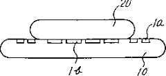
制作具有一个(100)取向主表面的直径为5英寸的第一和第二硅基片。通过热氧化或类似方法,在第一硅基片的表面上形成一个氧化物薄膜(未显示),接着加工成形在以后加工步骤中用于刻化氧化物薄膜图型1b的开口。用氧化物薄膜作为一个蚀刻掩膜,对第一硅基片10进行蚀刻,形成大约1μm深的槽。槽的深度可根据所需要的特定装置的特性而变化。然后除去用作掩膜的氧化硅薄膜,接着通过热氧化低温化学汽相沉积或其它方法形成一个厚度大约与槽2的深度相匹配的均匀的氧化物薄膜。之后,正如在图1(a)和图2(a)中所示,通过研磨及抛光除去该氧化物薄膜从而留下原位埋于槽中的部分,由此在第一硅基片10的内部形成器件装置分离氧化物薄膜图型1,以及在其边缘上形成校准氧化物薄膜图型1a。用一个单平板印刷的掩膜依此方法同时摹制氧化物薄膜图型1b和校准氧化物薄膜图型1a。需指出的是氧化物薄膜图型1a和1b也可为通过硅的局部氧化(LOCOS)来提供氧化物薄膜。First and second silicon substrates having a (100) oriented major surface having a diameter of 5 inches were fabricated. An oxide film (not shown) is formed on the surface of the first silicon substrate by thermal oxidation or the like, followed by processing to form openings for etching the oxide film pattern 1b in subsequent processing steps. Using the oxide film as an etching mask, the
正如在图2(b)中看到的第二硅基片20的边缘上有三个取向的平面(简写为OFs)8。这些平面中,第一个取向平面8a用于与第一硅基片10的取向平面7相结合,以便校准两个基片的结晶学取向。第二和第三取向平面8b和8c形成必要的长度以便将校准氧化物薄膜图型1a显露出来(例如在<110>方向长度为40毫米)。As seen in FIG. 2(b) there are three oriented planes (abbreviated as OFs) 8 on the edge of the
接着,正如在图1(b)中看到的,当适当放置第二和第三取向平面8b和8c,以使其不会覆盖住形成于第一硅基片上的校准氧化物薄膜图型1a时,第二硅基片20与第一硅基片10相联接。这样做的结果隐埋了位于与第二硅基片20界面的在第一硅基片10内形成的氧化物薄膜图型1b。然后联接成整体的基片在氧化气氛中于1100℃~1200℃下热处理2个小时以保证联接效果。Next, as seen in FIG. 1(b), when the second and third alignment planes 8b and 8c are properly positioned so as not to cover the alignment oxide film pattern 1a formed on the first silicon substrate , the
正如在图1(c)中看到的,通过研磨去除三个取向平面8的截面和第二硅基片20的边缘。正如在图1d中看到的,第二硅基片20的未联接的背面表面通过研磨及抛光变薄形成一个大约10μm厚的SOI层。该SOI层被设计成能保证装置的操作的厚度。最后,用稀释的氢氟酸腐蚀掉热处理期间在基片表面形成的一个不需要的氧化膜(未显示),从而提供一个联接的SOI基片100。As seen in FIG. 1(c), the sections of the three orientation planes 8 and the edge of the
如上面所述,根据本实施例的SOI基片100,在第一硅基片10的边缘上有显露的校准氧化物薄膜图型1a。这可容许用传统的可见光校准器通过掩膜进行校准,其精度为0.2μm的数量级。As described above, according to the
现在将参考SOI基片和掩膜的截面图图3来对校准方法做阐述。在图3中,在包含SOI层20a的SOI基片100的表面上提供光刻胶薄膜3。在SOI基片100的上面放置一个石英基片4,其通过在其上形成的掩膜图型而成为一个光刻掩模。在该掩膜图型中,校准掩膜图型5A沿石英基片4及基片I0上的校准氧化物薄膜图型1a的边缘部分放置而被用来通过可见光进行校准。这容许了处于石英基片4及氧化物薄膜图型1b之上的掩膜图型5B的高精度校准。之后,将在SOI层20a的表面上提供的光刻胶薄膜3暴露于例如波长为400nm的紫外线中,以将掩膜图型5B转换到光刻胶薄膜3上。前面所述的校准程序可以高精度来完成,因为它们可用已有技术中的光学校准器上来实现。The calibration method will now be described with reference to FIG. 3, a cross-sectional view of the SOI substrate and mask. In FIG. 3, a
这种应用具有校准图型的基片的掩膜校准方法保证了高精度的校准通过在形成有标准图型的第一硅基片的上成形器件及与第一硅晶片相联接的第二硅基片上成形器件的生产多层器件的工艺过程。This method of mask calibration using a substrate with a calibration pattern ensures high-precision calibration by forming devices on a first silicon substrate with a standard pattern and a second silicon wafer bonded to the first silicon wafer. A process for producing multilayer devices by forming devices on a substrate.
图4是根据本发明第二实施例描述的一个SOI基片100A的平面图。校准氧化物薄膜图型1a与第一实施例中相同的方式置于第一硅基片10的边缘。然而,V形槽部分9形成于第二硅基片20的边缘之上,且两个槽部分9用于将校准氧化物薄膜图型显露出来。FIG. 4 is a plan view of an SOI substrate 100A described according to a second embodiment of the present invention. The alignment oxide film pattern 1a is placed on the edge of the
现在阐述一种制造SOI基片100A的方法。第二硅基片20有两个大约2毫米长及大约2毫米宽的V形槽部分9。槽的形状可根据需要制定,例如,U形,梯形或长方形。第二硅基片20与第一硅基片10面对形成有校准氧化物薄膜图型1a的面对联接,从而通过槽部分9使氧化物薄膜图型1a显露出来。然后研磨及腐蚀第二硅基片20的边缘去掉非联接部分。最后,通过薄化形成SOI层20a,形成于基片表面上的不需要的氧化物薄膜被去除以形成SOI基片100A。A method of manufacturing the SOI substrate 100A will now be described. The
根据本实施例,由于通过提供比取向平面(OFs)面积小的槽部分而使校准图型显露出来,在给定直径的基片上可以获得比按照第一个实施例更多的芯片产品。这里,需要说明的是虽然前面描述的涉及具有两个槽部分的一个第二硅基片,但当然它也可提供3个或更多的槽。According to the present embodiment, since the alignment pattern is exposed by providing the groove portion smaller in area than the orientation flats (OFs), more chip products can be obtained on a substrate of a given diameter than according to the first embodiment. Here, it should be noted that although the foregoing description refers to a second silicon substrate having two groove portions, it is of course also possible to provide three or more grooves.
图5是根据本发明第三个实施例描述的SOI基片的平面图。与第一个实施例相似,校准氧化物薄膜图型1a置于第一硅基片10的边缘上,并通过研磨及腐蚀过程去除第二硅基片20的边缘而使其显露出来。由于硅基片的整个边缘被去除,因而可提供3个或更多的校准氧化物薄膜图型。现在将阐述一种制造基片的方法。按与第一实施例相似的方式,形成氧化物薄膜图型1a和1b然后制备第二硅基片20,并将其联接到包含成形于其上的氧化物薄膜图型1a和1b的第一硅基片10的表面上。这里,热处理的条件与第一个实施例中的条件一致。然后,沿着第二硅基片20的大约1毫米宽50μm量级厚的边缘,该复合物被浸入诸如氢氧化钾溶液的非匀质腐蚀溶液中去除由于研磨而显露出来的信号晶硅层。通过设定腐蚀时间及溶液温度以便使校准氧化物薄膜图型1a暴露出来。最后,形成SOI层20a,形成于基片表面的不需要的氧化物膜被去除而得到SOI基片1OOB。Fig. 5 is a plan view of an SOI substrate according to a third embodiment of the present invention. Similar to the first embodiment, the alignment oxide film pattern 1a is placed on the edge of the
与第一个实施例不同,本实施例不需要形成OFs,这保证可用传统的用于相关领域的单晶硅基片作为第二硅基片。另外,去除第二硅基片的边缘的结果同时也去除了非联接的部分以及在边缘部分常见的联接不紧的部分,从而其不会产生断裂及破损。Unlike the first embodiment, this embodiment does not require formation of OFs, which ensures that a conventional single crystal silicon substrate used in the related art can be used as the second silicon substrate. In addition, as a result of removing the edge of the second silicon substrate, the non-bonded portion and the loosely bonded portion that is common at the edge portion are also removed, so that it will not be cracked and damaged.
图6是根据本发明的第四个实施例描述的SOI基片的截面图。其特别显示了在形成的氧化物薄膜的第一硅基片而不是第二硅基片的背面被通过腐蚀或其它方法被去除掉,以形成一个SOI层及进一步使校准图型显露出来。Fig. 6 is a sectional view of an SOI substrate according to a fourth embodiment of the present invention. It specifically shows that the oxide film formed on the backside of the first silicon substrate but not the second silicon substrate is removed by etching or other methods to form an SOI layer and further reveal the alignment pattern.
更具体地说,在图6中,与第二硅基片20的表面相联接的是一有用校准氧化物薄膜图型1a和氧化物薄膜图型1b作为器件分离的第一硅基片10。然后用非匀质碱腐蚀剂研磨或处理第一硅基片10的背面以形成一个SOI层10a并使其边缘变薄至与氧化物薄膜相同的厚度,从而使校准氧化物薄膜图型1a显露出来。More specifically, in FIG. 6, coupled to the surface of the
根据本实施例,两基片的联接界面形成了隐埋氧化物薄膜图型1b的较低边界面。通过这种结构,在联接界面可能形成的空隙(未联接部分)或晶体缺陷,或者在联接过程中捕获的可能对器件性能造成负影响的杂质被隐埋的氧化物薄膜与SOI层10a隔开。相应地,一个具有如上所述结构的SOI基片100c,特别是处于隐埋氧化物薄膜上面的SOI层10a上的区域,保证了制造产生极少误差的高精度器件。According to this embodiment, the connection interface of the two substrates forms the lower boundary surface of the buried oxide thin film pattern 1b. With this structure, voids (unjoined portions) or crystal defects that may be formed at the joining interface, or impurities trapped during the joining process that may negatively affect device performance are separated from the SOI layer 10a by the buried oxide film. . Accordingly, an SOI substrate 100c having the structure as described above, especially the region on the SOI layer 10a above the buried oxide film, ensures the fabrication of high-precision devices with very few errors.
虽然通过某些最佳的实例对本发明进行了描述,必须明确由本发明所包含的主题范围不仅局限于这些特定实例。多种的改变,改进或变化也处于本发明主题的范围之中。Although the present invention has been described in terms of certain preferred examples, it must be understood that the scope of the subject matter encompassed by the present invention is not limited to these specific examples. Various modifications, improvements or variations are also within the scope of the inventive subject matter.
例如,与被隐埋的氧化物薄膜图型同时形成的校准氧化物薄膜图型,在加工SOI基片的步骤中只要处于视野范围之中其厚度可被任意确定(虽然其限度要根据器件的所需的性能来决定),且在校准时具有可识别的薄膜厚度(大约100nm或更大)。另外,虽然在本发明的实施例中形成的是氧化硅薄膜图型,该图型也可被制成诸如氮化硅薄膜(Si3N4)或掺杂的硅酸盐玻璃。另外,由于校准图型的形状可按照传统的使用可见光的校准方法来确定,图型形状可根据需要确定,例如,条形、长方形、直角点阵的或正交点阵的。For example, the alignment oxide film pattern formed simultaneously with the buried oxide film pattern can be arbitrarily determined as long as it is within the field of view in the step of processing the SOI substrate (although its limit depends on the device required performance), and have a recognizable film thickness (approximately 100nm or greater) when calibrated. In addition, although a silicon oxide film pattern is formed in the embodiment of the present invention, the pattern can also be formed such as a silicon nitride film (Si3 N4 ) or doped silicate glass. In addition, since the shape of the calibration pattern can be determined according to the traditional calibration method using visible light, the shape of the pattern can be determined according to needs, for example, bar shape, rectangle, rectangular lattice or orthogonal lattice.
如上所述,本发明通过将包含形成于硅基片边缘上的绝缘体膜的校准图型显露出来,从而可以容许用传统的光学校准器进行校准,并完成比用传输红外辐射的方法更高的精度校准。另外,本发明容许在制造含有成形于成形有校准图型的硅基片以及SOI层的表面上的器件的多层结构的半导体器件的步骤中产生高精度的校准。As described above, the present invention allows alignment with a conventional optical collimator by revealing an alignment pattern comprising an insulator film formed on the edge of a silicon substrate, and accomplishes a higher degree of alignment than by a method of transmitting infrared radiation. Accuracy Calibration. In addition, the present invention allows high-precision alignment to be produced in the step of manufacturing a semiconductor device including a multilayer structure of devices formed on the surface of a silicon substrate formed with an alignment pattern and an SOI layer.
Claims (14)
Translated fromChineseApplications Claiming Priority (2)
| Application Number | Priority Date | Filing Date | Title |
|---|---|---|---|
| JP251556/95 | 1995-09-28 | ||
| JP25155695 | 1995-09-28 |
Publications (2)
| Publication Number | Publication Date |
|---|---|
| CN1158004A CN1158004A (en) | 1997-08-27 |
| CN1078738Ctrue CN1078738C (en) | 2002-01-30 |
Family
ID=17224583
Family Applications (1)
| Application Number | Title | Priority Date | Filing Date |
|---|---|---|---|
| CN96119843AExpired - Fee RelatedCN1078738C (en) | 1995-09-28 | 1996-09-27 | Composite silicon-on-insulator substrate and method of fabricating the same |
Country Status (2)
| Country | Link |
|---|---|
| US (1) | US5869386A (en) |
| CN (1) | CN1078738C (en) |
Families Citing this family (30)
| Publication number | Priority date | Publication date | Assignee | Title |
|---|---|---|---|---|
| US6013355A (en)* | 1996-12-30 | 2000-01-11 | International Business Machines Corp. | Testing laminates with x-ray moire interferometry |
| JP3114643B2 (en)* | 1997-02-20 | 2000-12-04 | 日本電気株式会社 | Semiconductor substrate structure and manufacturing method |
| US20020164784A1 (en)* | 2000-10-27 | 2002-11-07 | Walke D. Wade | Novel human 7TM proteins and polynucleotides encoding the same |
| JP2000223683A (en)* | 1999-02-02 | 2000-08-11 | Canon Inc | Composite member and its separation method, bonded substrate and its separation method, transfer layer transfer method, and SOI substrate manufacturing method |
| US6558990B1 (en) | 1999-07-02 | 2003-05-06 | Mitsubishi Materials Silicon Corporation | SOI substrate, method of manufacture thereof, and semiconductor device using SOI substrate |
| US6350659B1 (en) | 1999-09-01 | 2002-02-26 | Agere Systems Guardian Corp. | Process of making semiconductor device having regions of insulating material formed in a semiconductor substrate |
| TW587332B (en) | 2000-01-07 | 2004-05-11 | Canon Kk | Semiconductor substrate and process for its production |
| US6166420A (en)* | 2000-03-16 | 2000-12-26 | International Business Machines Corporation | Method and structure of high and low K buried oxide for SoI technology |
| JP3991300B2 (en)* | 2000-04-28 | 2007-10-17 | 株式会社Sumco | Manufacturing method of bonded dielectric isolation wafer |
| JP2002050749A (en)* | 2000-07-31 | 2002-02-15 | Canon Inc | Method and apparatus for separating composite members |
| JP2003078115A (en)* | 2001-08-30 | 2003-03-14 | Shin Etsu Handotai Co Ltd | Soi wafer laser mark printing method and soi wafer |
| SG116475A1 (en)* | 2002-02-05 | 2005-11-28 | Taiwan Semiconductor Mfg | Bonded soi wafer with <100> device layer and <110>substrate for performance improvement. |
| US6784071B2 (en)* | 2003-01-31 | 2004-08-31 | Taiwan Semiconductor Manufacturing Company, Ltd. | Bonded SOI wafer with <100> device layer and <110> substrate for performance improvement |
| US7148211B2 (en)* | 2002-09-18 | 2006-12-12 | Genzyme Corporation | Formulation for lipophilic agents |
| US20040053895A1 (en)* | 2002-09-18 | 2004-03-18 | Bone Care International, Inc. | Multi-use vessels for vitamin D formulations |
| US20040058895A1 (en)* | 2002-09-18 | 2004-03-25 | Bone Care International, Inc. | Multi-use vessels for vitamin D formulations |
| JP2004119943A (en)* | 2002-09-30 | 2004-04-15 | Renesas Technology Corp | Semiconductor wafer and method of manufacturing the same |
| US6908565B2 (en)* | 2002-12-24 | 2005-06-21 | Intel Corporation | Etch thinning techniques for wafer-to-wafer vertical stacks |
| JP4066889B2 (en)* | 2003-06-09 | 2008-03-26 | 株式会社Sumco | Bonded substrate and manufacturing method thereof |
| FR2860842B1 (en)* | 2003-10-14 | 2007-11-02 | Tracit Technologies | PROCESS FOR PREPARING AND ASSEMBLING SUBSTRATES |
| US20060141744A1 (en)* | 2004-12-27 | 2006-06-29 | Asml Netherlands B.V. | System and method of forming a bonded substrate and a bonded substrate product |
| FR2899594A1 (en) | 2006-04-10 | 2007-10-12 | Commissariat Energie Atomique | METHOD FOR ASSEMBLING SUBSTRATES WITH THERMAL TREATMENTS AT LOW TEMPERATURES |
| JP4468427B2 (en) | 2007-09-27 | 2010-05-26 | 株式会社東芝 | Manufacturing method of semiconductor device |
| FR2925223B1 (en)* | 2007-12-18 | 2010-02-19 | Soitec Silicon On Insulator | METHOD FOR ASSEMBLING WITH ENTERED LABELS |
| CN103943464A (en)* | 2014-05-04 | 2014-07-23 | 上海先进半导体制造股份有限公司 | Alignment mark forming method |
| CN104078405A (en)* | 2014-06-24 | 2014-10-01 | 上海天英微系统科技有限公司 | Photoetching alignment method and wafers |
| US10163674B2 (en)* | 2014-11-27 | 2018-12-25 | National Institute Of Advanced Industrial Science And Technology | Circular support substrate for semiconductor |
| US9490154B2 (en)* | 2015-01-15 | 2016-11-08 | Applied Materials, Inc. | Method of aligning substrate-scale mask with substrate |
| US10680150B2 (en)* | 2017-08-15 | 2020-06-09 | Dragan Grubisik | Electrically conductive-semitransparent solid state infrared emitter apparatus and method of use thereof |
| CN112530908B (en)* | 2019-09-18 | 2023-12-26 | 芯恩(青岛)集成电路有限公司 | Preparation method of semiconductor device and semiconductor device |
Citations (2)
| Publication number | Priority date | Publication date | Assignee | Title |
|---|---|---|---|---|
| JPH02312220A (en)* | 1989-05-26 | 1990-12-27 | Nec Corp | Aligner |
| US5294556A (en)* | 1990-07-20 | 1994-03-15 | Fujitsu Limited | Method for fabricating an SOI device in alignment with a device region formed in a semiconductor substrate |
Family Cites Families (7)
| Publication number | Priority date | Publication date | Assignee | Title |
|---|---|---|---|---|
| US4599792A (en)* | 1984-06-15 | 1986-07-15 | International Business Machines Corporation | Buried field shield for an integrated circuit |
| JPH0429353A (en)* | 1990-05-24 | 1992-01-31 | Sharp Corp | Semiconductor device |
| JP3174786B2 (en)* | 1991-05-31 | 2001-06-11 | 富士通株式会社 | Method for manufacturing semiconductor device |
| JP2602597B2 (en)* | 1991-12-27 | 1997-04-23 | 信越半導体株式会社 | Method for manufacturing thin film SOI substrate |
| JP2729005B2 (en)* | 1992-04-01 | 1998-03-18 | 三菱電機株式会社 | Semiconductor pressure sensor and method of manufacturing the same |
| US5478782A (en)* | 1992-05-25 | 1995-12-26 | Sony Corporation | Method bonding for production of SOI transistor device |
| US5496764A (en)* | 1994-07-05 | 1996-03-05 | Motorola, Inc. | Process for forming a semiconductor region adjacent to an insulating layer |
- 1996
- 1996-09-23USUS08/710,851patent/US5869386A/ennot_activeExpired - Fee Related
- 1996-09-27CNCN96119843Apatent/CN1078738C/ennot_activeExpired - Fee Related
Patent Citations (2)
| Publication number | Priority date | Publication date | Assignee | Title |
|---|---|---|---|---|
| JPH02312220A (en)* | 1989-05-26 | 1990-12-27 | Nec Corp | Aligner |
| US5294556A (en)* | 1990-07-20 | 1994-03-15 | Fujitsu Limited | Method for fabricating an SOI device in alignment with a device region formed in a semiconductor substrate |
Also Published As
| Publication number | Publication date |
|---|---|
| US5869386A (en) | 1999-02-09 |
| CN1158004A (en) | 1997-08-27 |
Similar Documents
| Publication | Publication Date | Title |
|---|---|---|
| CN1078738C (en) | Composite silicon-on-insulator substrate and method of fabricating the same | |
| US20020168837A1 (en) | Method of fabricating silicon devices on sapphire with wafer bonding | |
| JP5188672B2 (en) | Manufacturing method of composite substrate | |
| EP0460437A2 (en) | Method of manufacturing semiconductor substrate and method of manufacturing semiconductor device composed of the substrate | |
| KR20000005859A (en) | Method for manufactuting soi wafer and soi wafer | |
| US6013954A (en) | Semiconductor wafer having distortion-free alignment regions | |
| KR100297867B1 (en) | Insulator type silicon semiconductor integrated circuit manufacturing method | |
| CN1502127A (en) | Semiconductor devices and their formation processes | |
| JP2870492B2 (en) | SOI substrate and manufacturing method thereof | |
| WO1998057361A1 (en) | Substrate for device manufacturing, process for manufacturing the substrate, and method of exposure using the substrate | |
| US6303509B1 (en) | Method to calibrate the wafer transfer for oxide etcher (with clamp) | |
| US7989894B2 (en) | Fusion bonding process and structure for fabricating silicon-on-insulation (SOI) semiconductor devices | |
| JP2561735B2 (en) | Liquid crystal display manufacturing method | |
| JPH06204776A (en) | Manufacture of piezoelectric thin film vibrator | |
| US6469361B2 (en) | Semiconductor wafer | |
| JP2008203851A (en) | Gray scale mask manufacturing method using wafer bonding process | |
| JP4439935B2 (en) | Manufacturing method of semiconductor device | |
| JP3061021B2 (en) | Partial SOI substrate and manufacturing method thereof | |
| JP3524009B2 (en) | SOI wafer and method for manufacturing the same | |
| JPH0114694B2 (en) | ||
| WO2002048765A1 (en) | Integrated optical devices | |
| KR0161467B1 (en) | Planarization method of semiconductor device | |
| KR100253586B1 (en) | Method for manufacturing cell aperture mask of semiconductor device | |
| US20070184580A1 (en) | Method of making a small substrate compatible for processing | |
| JPH03268444A (en) | Manufacturing method of semiconductor device |
Legal Events
| Date | Code | Title | Description |
|---|---|---|---|
| C10 | Entry into substantive examination | ||
| SE01 | Entry into force of request for substantive examination | ||
| C06 | Publication | ||
| PB01 | Publication | ||
| C14 | Grant of patent or utility model | ||
| GR01 | Patent grant | ||
| ASS | Succession or assignment of patent right | Owner name:NEC ELECTRONICS TAIWAN LTD. Free format text:FORMER OWNER: NIPPON ELECTRIC CO., LTD. Effective date:20030530 | |
| C41 | Transfer of patent application or patent right or utility model | ||
| TR01 | Transfer of patent right | Effective date of registration:20030530 Address after:Kanagawa, Japan Patentee after:NEC Corp. Address before:Tokyo, Japan Patentee before:NEC Corp. | |
| C19 | Lapse of patent right due to non-payment of the annual fee | ||
| CF01 | Termination of patent right due to non-payment of annual fee |