CN107851649B - Imaging device, manufacturing method, semiconductor device, and electronic device - Google Patents
Imaging device, manufacturing method, semiconductor device, and electronic deviceDownload PDFInfo
- Publication number
- CN107851649B CN107851649BCN201680040918.6ACN201680040918ACN107851649BCN 107851649 BCN107851649 BCN 107851649BCN 201680040918 ACN201680040918 ACN 201680040918ACN 107851649 BCN107851649 BCN 107851649B
- Authority
- CN
- China
- Prior art keywords
- diffusion layer
- photoelectric conversion
- conversion unit
- floating diffusion
- impurity concentration
- Prior art date
- Legal status (The legal status is an assumption and is not a legal conclusion. Google has not performed a legal analysis and makes no representation as to the accuracy of the status listed.)
- Active
Links
Images


Classifications
- H—ELECTRICITY
- H04—ELECTRIC COMMUNICATION TECHNIQUE
- H04N—PICTORIAL COMMUNICATION, e.g. TELEVISION
- H04N25/00—Circuitry of solid-state image sensors [SSIS]; Control thereof
- H04N25/70—SSIS architectures; Circuits associated therewith
- H04N25/76—Addressed sensors, e.g. MOS or CMOS sensors
- H—ELECTRICITY
- H04—ELECTRIC COMMUNICATION TECHNIQUE
- H04N—PICTORIAL COMMUNICATION, e.g. TELEVISION
- H04N25/00—Circuitry of solid-state image sensors [SSIS]; Control thereof
- H04N25/10—Circuitry of solid-state image sensors [SSIS]; Control thereof for transforming different wavelengths into image signals
- H04N25/17—Colour separation based on photon absorption depth, e.g. full colour resolution obtained simultaneously at each pixel location
- H—ELECTRICITY
- H10—SEMICONDUCTOR DEVICES; ELECTRIC SOLID-STATE DEVICES NOT OTHERWISE PROVIDED FOR
- H10F—INORGANIC SEMICONDUCTOR DEVICES SENSITIVE TO INFRARED RADIATION, LIGHT, ELECTROMAGNETIC RADIATION OF SHORTER WAVELENGTH OR CORPUSCULAR RADIATION
- H10F39/00—Integrated devices, or assemblies of multiple devices, comprising at least one element covered by group H10F30/00, e.g. radiation detectors comprising photodiode arrays
- H10F39/10—Integrated devices
- H10F39/12—Image sensors
- H—ELECTRICITY
- H10—SEMICONDUCTOR DEVICES; ELECTRIC SOLID-STATE DEVICES NOT OTHERWISE PROVIDED FOR
- H10F—INORGANIC SEMICONDUCTOR DEVICES SENSITIVE TO INFRARED RADIATION, LIGHT, ELECTROMAGNETIC RADIATION OF SHORTER WAVELENGTH OR CORPUSCULAR RADIATION
- H10F39/00—Integrated devices, or assemblies of multiple devices, comprising at least one element covered by group H10F30/00, e.g. radiation detectors comprising photodiode arrays
- H10F39/80—Constructional details of image sensors
- H10F39/803—Pixels having integrated switching, control, storage or amplification elements
- H10F39/8037—Pixels having integrated switching, control, storage or amplification elements the integrated elements comprising a transistor
- G—PHYSICS
- G06—COMPUTING OR CALCULATING; COUNTING
- G06T—IMAGE DATA PROCESSING OR GENERATION, IN GENERAL
- G06T2207/00—Indexing scheme for image analysis or image enhancement
- G06T2207/10—Image acquisition modality
- G—PHYSICS
- G09—EDUCATION; CRYPTOGRAPHY; DISPLAY; ADVERTISING; SEALS
- G09G—ARRANGEMENTS OR CIRCUITS FOR CONTROL OF INDICATING DEVICES USING STATIC MEANS TO PRESENT VARIABLE INFORMATION
- G09G2310/00—Command of the display device
- G09G2310/02—Addressing, scanning or driving the display screen or processing steps related thereto
- G09G2310/0264—Details of driving circuits
- G—PHYSICS
- G09—EDUCATION; CRYPTOGRAPHY; DISPLAY; ADVERTISING; SEALS
- G09G—ARRANGEMENTS OR CIRCUITS FOR CONTROL OF INDICATING DEVICES USING STATIC MEANS TO PRESENT VARIABLE INFORMATION
- G09G2320/00—Control of display operating conditions
- G09G2320/02—Improving the quality of display appearance
- H—ELECTRICITY
- H04—ELECTRIC COMMUNICATION TECHNIQUE
- H04N—PICTORIAL COMMUNICATION, e.g. TELEVISION
- H04N23/00—Cameras or camera modules comprising electronic image sensors; Control thereof
- H04N23/80—Camera processing pipelines; Components thereof
- H04N23/84—Camera processing pipelines; Components thereof for processing colour signals
- H04N23/843—Demosaicing, e.g. interpolating colour pixel values
- H—ELECTRICITY
- H04—ELECTRIC COMMUNICATION TECHNIQUE
- H04N—PICTORIAL COMMUNICATION, e.g. TELEVISION
- H04N25/00—Circuitry of solid-state image sensors [SSIS]; Control thereof
- H04N25/10—Circuitry of solid-state image sensors [SSIS]; Control thereof for transforming different wavelengths into image signals
- H04N25/11—Arrangement of colour filter arrays [CFA]; Filter mosaics
- H04N25/13—Arrangement of colour filter arrays [CFA]; Filter mosaics characterised by the spectral characteristics of the filter elements
- H04N25/134—Arrangement of colour filter arrays [CFA]; Filter mosaics characterised by the spectral characteristics of the filter elements based on three different wavelength filter elements
Landscapes
- Engineering & Computer Science (AREA)
- Multimedia (AREA)
- Signal Processing (AREA)
- Solid State Image Pick-Up Elements (AREA)
- Transforming Light Signals Into Electric Signals (AREA)
- Electrodes Of Semiconductors (AREA)
Abstract
Description
Translated fromChinese技术领域technical field
本公开涉及一种成像设备、制造方法、半导体设备和电子设备,特别地,涉及一种可以进一步提高图像质量的成像设备、制造方法、半导体设备和电子设备。The present disclosure relates to an imaging device, a manufacturing method, a semiconductor device, and an electronic device, and in particular, to an imaging device, a manufacturing method, a semiconductor device, and an electronic device that can further improve image quality.
背景技术Background technique
通常,存在通过与CMOS(互补金属氧化物半导体)集成电路类似的处理制造的被称为固态成像设备的CMOS固态成像设备(在下文中称为CMOS图像传感器)。Generally, there is a CMOS solid-state imaging device (hereinafter referred to as a CMOS image sensor) called a solid-state imaging device manufactured by a process similar to a CMOS (Complementary Metal Oxide Semiconductor) integrated circuit.
在CMOS图像传感器中,与CMOS处理有关的微型化技术可用于容易地生产在每一个像素中具有放大功能的有源结构。CMOS图像传感器同样具有允许将外围电路单元(诸如驱动像素阵列单元的驱动电路和处理从像素阵列单元的每一个像素输出的信号的信号处理电路)整合在与像素阵列单元的芯片相同的芯片(基底)上的特性。因此,CMOS图像传感器引起人们的注意,对CMOS进行了很多研究和开发。In CMOS image sensors, miniaturization techniques associated with CMOS processing can be used to easily produce active structures with amplification in each pixel. The CMOS image sensor also has a chip (substrate) that allows peripheral circuit units (such as a driver circuit that drives the pixel array unit and a signal processing circuit that processes a signal output from each pixel of the pixel array unit) to be integrated on the same chip as that of the pixel array unit. ) features. Therefore, CMOS image sensors have attracted attention, and much research and development of CMOS has been carried out.
同样,作为聚集和读取CMOS图像传感器的电荷的方法,通常采用这样的结构,其中电荷聚集在PD(光电二极管)中,转移晶体管用来将电荷转移至包括具有预定量的电荷积聚的浮动扩散层FD(浮动扩散)单元,并且读取该电荷。Also, as a method of accumulating and reading electric charges of a CMOS image sensor, a structure is generally adopted in which electric charges are accumulated in a PD (photodiode), and a transfer transistor is used to transfer electric charges to a floating diffusion including electric charge accumulation having a predetermined amount Layer FD (Floating Diffusion) cells, and read the charge.
近年来,提出了如在PTL1、PTL2和PTL3的第四实施方案中公开的结构,其中CMOS图像传感器的光电变换单元布置在半导体基底的上部,光电变换信号被聚集在半导体基底中。In recent years, a structure as disclosed in the fourth embodiment of PTL1, PTL2 and PTL3 has been proposed in which the photoelectric conversion unit of the CMOS image sensor is arranged on the upper part of the semiconductor substrate in which the photoelectric conversion signal is collected.
[引用列表][quote list]
[专利文献][Patent Literature]
[PTL1]JP2007-329161A[PTL1] JP2007-329161A
[PTL2]JP2010-278086A[PTL2] JP2010-278086A
[PTL3]JP2011-138927A[PTL3] JP2011-138927A
发明内容SUMMARY OF THE INVENTION
技术问题technical problem
顺便提及,在CMOS图像传感器中,缺陷源诸如金属杂质偶而会聚集在构成制造方法中聚集电荷的FD单元的高浓度杂质扩散层中。因此,FD单元中可能会生产生噪声,并且图像特性可能会由于CMOS图像传感器获取的图像中出现的白点、白痕、黑点等等而劣化。这可能会降低图像质量。Incidentally, in a CMOS image sensor, a defect source such as a metal impurity occasionally accumulates in a high-concentration impurity diffusion layer constituting an FD cell that collects charges in a manufacturing method. Therefore, noise may be generated in the FD unit, and image characteristics may be deteriorated due to white spots, white streaks, black spots, and the like appearing in images acquired by the CMOS image sensor. This may reduce image quality.
鉴于这种情况,进行了本公开,并且本公开可以进一步提高图像质量。问题的解决方案The present disclosure has been made in view of this situation, and the present disclosure can further improve image quality. solution to the problem
根据本公开的一方面的成像设备包括接收光并对其进行光电转换的光电转换单元、聚集该光电转换单元产生的电荷的浮动扩散层和充当晶体管的源极或漏极的扩散层。该浮动扩散层形成为具有比该扩散层的杂质浓度低的杂质浓度。An imaging apparatus according to an aspect of the present disclosure includes a photoelectric conversion unit that receives and photoelectrically converts light, a floating diffusion layer that collects charges generated by the photoelectric conversion unit, and a diffusion layer that serves as a source or drain of a transistor. The floating diffusion layer is formed to have an impurity concentration lower than that of the diffusion layer.
根据本公开的一方面的制造方法是成像设备的制造方法,该成像设备包括接收光并对其进行光电转换的光电转换单元、聚集该光电转换单元产生的电荷的浮动扩散层和充当晶体管的源极或漏极的扩散层。该制造方法分别地包括形成该浮动扩散层的步骤和形成该扩散层的步骤。该浮动扩散层形成为具有比该扩散层的杂质浓度低的杂质浓度。A manufacturing method according to an aspect of the present disclosure is a manufacturing method of an imaging device including a photoelectric conversion unit that receives light and photoelectrically converts it, a floating diffusion layer that collects charges generated by the photoelectric conversion unit, and a source serving as a transistor Diffusion layer of the electrode or drain. The manufacturing method includes a step of forming the floating diffusion layer and a step of forming the diffusion layer, respectively. The floating diffusion layer is formed to have an impurity concentration lower than that of the diffusion layer.
根据本公开的一方面的半导体设备包括聚集电荷的浮动扩散层和充当晶体管的源极或漏极的扩散层。该浮动扩散层形成为具有比该扩散层的杂质浓度低的杂质浓度。A semiconductor device according to an aspect of the present disclosure includes a floating diffusion layer that collects charges and a diffusion layer that serves as a source or drain of a transistor. The floating diffusion layer is formed to have an impurity concentration lower than that of the diffusion layer.
根据本公开的一方面的电子设备包括成像设备。该成像设备包括接收光并对其进行光电转换的光电转换单元、聚集该光电转换单元产生的电荷的浮动扩散层和充当晶体管的源极或漏极的扩散层。该浮动扩散层形成为具有比该扩散层的杂质浓度低的杂质浓度。An electronic device according to an aspect of the present disclosure includes an imaging device. The imaging device includes a photoelectric conversion unit that receives light and photoelectrically converts it, a floating diffusion layer that collects charges generated by the photoelectric conversion unit, and a diffusion layer that serves as a source or drain electrode of a transistor. The floating diffusion layer is formed to have an impurity concentration lower than that of the diffusion layer.
在本公开的一方面,关于聚集电荷的浮动扩散层和充当晶体管的源极或漏极的扩散层,该浮动扩散层形成为具有比该扩散层的杂质浓度低的杂质浓度。In an aspect of the present disclosure, regarding a floating diffusion layer that accumulates charges and a diffusion layer serving as a source or drain of a transistor, the floating diffusion layer is formed to have an impurity concentration lower than that of the diffusion layer.
本发明的有益效果The beneficial effects of the present invention
根据本公开的一方面,图像质量可以得到进一步提高。According to an aspect of the present disclosure, image quality can be further improved.
附图说明Description of drawings
[图1]图1是描述应用本技术的成像设备的实施方案的配置实例的方框图。[ Fig. 1] Fig. 1 is a block diagram illustrating a configuration example of an embodiment of an imaging apparatus to which the present technology is applied.
[图2]图2是描述像素的第一配置实例的示意图。[ Fig. 2] Fig. 2 is a schematic diagram describing a first configuration example of a pixel.
[图3]图3是描述第一步骤的示意图。[ Fig. 3] Fig. 3 is a schematic diagram describing the first step.
[图4]图4是描述第二步骤的示意图。[ Fig. 4] Fig. 4 is a schematic diagram describing the second step.
[图5]图5是描述第三步骤的示意图。[ Fig. 5] Fig. 5 is a schematic diagram describing the third step.
[图6]图6是描述第四步骤的示意图。[ Fig. 6] Fig. 6 is a schematic diagram describing the fourth step.
[图7]图7是描述第五步骤的示意图。[ Fig. 7] Fig. 7 is a schematic diagram describing the fifth step.
[图8]图8是描述第六步骤的示意图。[ Fig. 8] Fig. 8 is a schematic diagram describing the sixth step.
[图9]图9是描述第七步骤的示意图。[ Fig. 9] Fig. 9 is a schematic diagram describing the seventh step.
[图10]图10是描述像素的修改例的示意图。[ Fig. 10] Fig. 10 is a schematic diagram describing a modification example of a pixel.
[图11]图11是描述避免肖特基结的示意图。[ Fig. 11] Fig. 11 is a schematic diagram describing the avoidance of a Schottky junction.
[图12]图12是描述像素的第二配置实例的示意图。[ Fig. 12] Fig. 12 is a schematic diagram describing a second configuration example of a pixel.
[图13]图13是描述像素的第三配置实例的示意图。[ Fig. 13] Fig. 13 is a schematic diagram describing a third configuration example of a pixel.
[图14]图14是描述使用图像传感器的使用实例的示意图。[ Fig. 14] Fig. 14 is a schematic diagram describing a use example using an image sensor.
[图15]图15是描述应用本技术的电子设备的实施方案的配置实例的方框图。[ Fig. 15] Fig. 15 is a block diagram describing a configuration example of an embodiment of an electronic apparatus to which the present technology is applied.
具体实施方案specific implementation
在下文,将参考附图详细描述应用本技术的具体的实施方案。Hereinafter, specific embodiments to which the present technology is applied will be described in detail with reference to the accompanying drawings.
<图像设备的配置实例><Configuration example of image device>
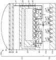
图1是描述应用本技术的成像设备的实施方案的配置实例的方框图。FIG. 1 is a block diagram describing a configuration example of an embodiment of an imaging apparatus to which the present technology is applied.
如图1中所描述的,成像设备11包括像素区域12、垂直驱动电路13、列信号处理电路14、水平驱动电路15、输出电路16和控制电路17。As described in FIG. 1 , the
像素区域12是用于接收由光学系统(未描述)聚集的光的光接收表面。多个像素21布置在像素区域12的矩阵中。每一个像素21通过各行的水平信号线22连接至垂直驱动电路13,每一个像素21通过各列的垂直信号线23连接至列信号处理电路14。该多个像素21的每一个根据所接收的光的量输出一个电平的像素信号,在像素区域12中形成的对象的图像由像素信号构成。The
对于布置在像素区域12中的多个像素21的各行,垂直驱动电路13通过水平信号线路22顺序地提供用于驱动(转移、选择、重置等等)像素21至像素21的驱动信号。For each row of the plurality of
列信号处理电路14通过垂直信号线23将CDS(相关双采样)处理应用于从多个像素21输出的像素信号,从而执行像素信号的AD(模数)转换并且去除重置噪声。The column
对于布置在像素区域12中的多个像素21的各列,水平驱动电路15顺序地向列信号处理电路14提供用于使列信号处理电路14向数据输出信号线24输出像素信号的驱动信号。For each column of the plurality of
输出电路16在根据水平驱动电路15的驱动信号的时间通过数据输出信号线24将从列信号处理电路14提供的像素信号放大至预定电平并且输出该像素信号。The
控制电路17根据构成成像设备11的各个块的驱动周期产生并且提供时钟信号,从而控制各个块的驱动。The
成像设备11这样构成,并且根据像素21收到的光的量的像素信号被顺序地输出到随后阶段的信号处理电路(未描述)。成像设备11还可以具有例如背照式结构,其中将光照射到面对像素21的PD形成的半导体基底的正面的相对侧的背面。The
<像素的第一配置实例><First configuration example of pixels>
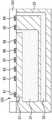
接下来,图2是描述像素21的第一配置实例的示意图。Next, FIG. 2 is a schematic diagram describing a first configuration example of the
如图2中所描述,像素21通过在设置有红色PD31和蓝色PD32的半导体基底33的正面(图2中面向下的表面)上层压布线层34,并且在半导体基底33的背面(图2中面向上的表面)上层压绝缘薄膜35、下部电极36、绿色光电转换薄膜37、上部电极38和片上透镜39而构成。As described in FIG. 2 , the
红色PD31是光电转换单元,其包括在半导体基底33的背面上的较深区域中形成的N型扩散层和P型扩散层的PN结,并且红色PD31对红光进行光电转换和聚集。蓝色PD32是光电转换单元,其包括在半导体基底33的背面上的较浅的区域中形成的N型扩散层和P型扩散层的PN结,并且蓝色PD32对蓝色光进行光电转换和聚集。The
半导体基底33是例如包括切成薄片的单晶硅的板状晶圆片。半导体基底33的正面配置有如下描述的多个N型扩散层并且配置有根据施加在栅电极的电压控制电流的多个晶体管,其中该N型扩散层充当源极或者漏极。The
布线层34配置有用于通过层间绝缘薄膜在层中传输驱动像素21的驱动信号、从像素21输出的像素信号等的多个布线。The
绝缘薄膜35使半导体基底33的背面绝缘。The insulating
下部电极36和38由导电透明材料形成并且被分层以便夹住绿色光电转换薄膜37。The
绿色光电转换薄膜37吸收绿光并且对其进行光电转换,由传输除了绿光以外的光的有机材料形成。将由绿色光电转换薄膜37产生的电荷通过连接至下部电极36的接触电极41顺序地取出,并且接触电极41在穿过半导体基底33的部分由绝缘薄膜42绝缘。The green
片上透镜39将照射到像素21的光进行聚集。The on-
这样配置的像素21具有纵向分光结构,其中红色PD31、蓝色PD32和绿色光电转换薄膜37在沿着照射到像素21的光的照射方向的纵向上布置。另外,红、蓝和绿光可以在一个像素21中进行光电转换。The
与例如具有包括布置在平面上的红、蓝和绿色滤色器的像素阵列的结构相比,具有使用该纵向分光结构的像素21的结构的成像设备11可以抑制由于滤色器的光吸收引起的感光性的降低。此外,使用纵向分光结构的像素21的配置不需要插值处理,并且可以预期避免产生假色的有益效果。The
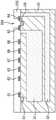
这里,半导体基底33(P阱)连接至基准电位。N型扩散层51至59形成在半导体基底33的正面上,栅电极61至68通过绝缘薄膜形成在半导体基底33的正面上。Here, the semiconductor substrate 33 (P well) is connected to the reference potential. N-type diffusion layers 51 to 59 are formed on the front surface of the
接触电极71在半导体基底33和布线层34之间的交界面处连接至N型扩散层51,N型扩散层51通过接触电极71、布线72和接触电极41连接至下部电极36。更具体地,N型扩散层51构成聚集由绿色光电转换薄膜37产生的电荷的FD单元81。The
N型扩散层52连接至基准电位(GND)。The N-
另外,N型扩散层51和52,连同布置在N型扩散层51和52之间的栅电极61,构成重置FD单元81的重置晶体管82。更具体地,根据从垂直驱动电路13提供的重置信号RST1驱动重置晶体管82以将聚集在N型扩散层51中的电荷输出至基准电位(GND)来重置FD单元81。In addition, the N-type diffusion layers 51 and 52 , together with the
N型扩散层53连接至漏极电源VDD。N型扩散层53和54,连同布置在N型扩散层53和54之间的栅电极62,构成对聚集在FD单元81中的电荷进行放大的放大晶体管83。更具体地说,栅电极62通过接触电极73、布线72和接触电极71连接至FD单元81,并且将根据FD单元81中聚集的电荷的电平的电位施加于栅电极62。因而,聚集在FD单元81的电荷由放大晶体管83放大并且转换为像素信号。The N-
N型扩散层55连接至垂直信号线23。N型扩散层54和55,连同布置在N型扩散层54和55之间的栅电极63,构成在输出像素信号的时刻选择像素21的选择晶体管84。更具体地说,根据从垂直驱动电路13提供的选择信号SEL1驱动选择晶体管84以将放大晶体管83连接至垂直信号线23。The N-
N型扩散层56构成FD单元85,FD单元85聚集红色PD31产生的各电荷和蓝色PD32产生的电荷。The N-
N型扩散层56,连同布置在N型扩散层56和延伸至半导体基底33的正面的蓝色PD32的一部分之间的栅电极64,也构成将蓝色PD32产生的电荷转移至FD单元85的转移晶体管86。更具体地说,根据从垂直驱动电路13提供的转移信号TGB驱动转移晶体管86以将聚集在蓝色PD32中的电荷转移至FD单元85。The N-
同样地,N型扩散层56,连同布置在N型扩散层56和延伸至半导体基底33的正面的红色PD31的一部分之间的栅电极65,也构成将红色PD31产生的电荷转移至FD单元85的转移晶体管87。更具体地说,根据从垂直驱动电路13提供的转移信号TGR驱动转移晶体管87以将聚集在红色PD31中的电荷转移至FD单元85。Likewise, the N-
另外,构成FD单元85的N型扩散层56通过接触电极74、布线75和接触电极76连接至布置在N型扩散层57和58之间的栅电极66。In addition, the N-
N型扩散层57和58,连同布置在N型扩散层57和58之间的栅电极66,构成对聚集在FD单元85中的电荷进行放大的放大晶体管88。更具体地说,将根据聚集在FD单元85的电荷的电平的电位施加于放大晶体管88的栅电极66,并且电荷由放大晶体管88放大并且转换为像素信号。The N-type diffusion layers 57 and 58 , together with the
N型扩散层59连接至漏极电源VDD,并且N型扩散层59,连同N型扩散层56和栅电极68,构成重置FD单元85的重置晶体管90。更具体地,根据从垂直驱动电路13提供的重置信号RST1驱动重置晶体管90以将聚集在N型扩散层56中的电荷输出至基准电位(GND)来重置FD单元85。The N-
这样,像素21形成为使得设置在半导体基底33的正面上的N型扩散层51至59中的、聚集由绿色光电转换薄膜37产生的电荷的N型扩散层51的杂质浓度是比其他N型扩散层52至59更低的浓度。这样,N型扩散层51的杂质浓度可以设置为低浓度来防止缺陷源(诸如半导体基底33中包含的金属杂质)在N型扩散层51中积聚,并且避免图像特性的劣化。In this way, the
具体地,优选地将N型扩散层51的杂质浓度设置为1e18至1e20/cm3并且将N型扩散层52至59的杂质浓度设置为1e20/cm3或更大。Specifically, it is preferable to set the impurity concentration of the N-
因此,在包括像素21的成像设备11摄取的图像中不产生白点、白痕、黑点等,并且图像质量可以比传统成像设备的更高。此外,可以预期提高成像设备11的市场性和提高产量的有益效果。Therefore, white spots, white streaks, black spots, etc. are not generated in the image captured by the
此外,像素21具有这样的结构,其中聚集电荷的红色PD31和蓝色PD32以及电荷从其中顺序地被取出并且聚集在FD单元81中的绿色光电转换薄膜37位于同一个半导体基底33上。在这种配置中,优选将聚集绿色光电转换薄膜的电荷的FD单元81的杂质浓度设置为比接收红色PD31和蓝色PD32产生的电荷的FD单元85的杂质浓度更低的浓度。这样可以防止FD单元81中聚集的缺陷源。特别地,在聚集FD单元81中的电荷的结构中,电荷的聚集时间长,并且防止缺陷源在FD单元81中积聚的有益效果可以很大。Further, the
其次,参照图3至9描述了在制造包括像素21的成像设备11的方法中形成具有不同杂质浓度的N型扩散层的步骤。Next, steps of forming N-type diffusion layers having different impurity concentrations in the method of manufacturing the
首先,如图3中所描述,将N型和P型杂质的离子注入应用于半导体基底33以形成红色PD31和蓝色PD32,栅电极61至68通过第一步骤的绝缘薄膜形成在半导体基底33的正面上。First, as described in FIG. 3, ion implantation of N-type and P-type impurities is applied to the
接下来,如图4所述,在第二步骤中,将抗蚀剂101沉积在半导体基底33的正面上,并在设置有N型扩散层51的区域形成开口102。然后通过开口102施加N型杂质的离子注入以形成N型扩散层51。在这种情况下,栅电极61,连同开口102,被用作定义用于形成N型扩散层51的区域的图案的一部分。Next, as described in FIG. 4 , in the second step, a resist 101 is deposited on the front surface of the
然后,如图5中所述,在第三步骤中,将抗蚀剂101从半导体基底33的正面移除。Then, as described in FIG. 5 , in a third step, the resist 101 is removed from the front surface of the
接下来,如图6所述,在第四步骤中,将抗蚀剂103沉积在半导体基底33的正面上,并在设置有N型扩散层56的区域形成开口104。然后通过开口104施加N型杂质的离子注入以形成N型扩散层56。在这种情况下,栅电极64和65,连同开口104,被用作定义用于形成N型扩散层56的区域的图案的一部分。Next, as described in FIG. 6 , in a fourth step, a resist 103 is deposited on the front surface of the
然后,如图7中所述,在第五步骤中,将抗蚀剂103从半导体基底33的正面移除。Then, as described in FIG. 7 , in a fifth step, the resist 103 is removed from the front surface of the
接下来,如图8中所述,在第六步骤中,将抗蚀剂105沉积在半导体基底33的正面,并且在设置N型扩散层52至55和N型扩散层57至59的区域中形成开口106。然后通过开口104施加N型杂质的离子注入以形成N型扩散层52至55和N型扩散层57至59。在这种情况下,栅电极61至63和栅电极66至68,连同开口106,被用作定义用于形成N型扩散层52至55和N型扩散层57至59的区域的图案的一部分。Next, as described in FIG. 8, in a sixth step, a resist 105 is deposited on the front surface of the
接下来,如图9中所述,在第七步骤中,将抗蚀剂105从半导体基底33的正面移除。Next, as described in FIG. 9 , in a seventh step, the resist 105 is removed from the front surface of the
如上所述,在第一至第七步骤的不同步骤中各自形成N型扩散层51、N型扩散层56、N型扩散层52至55和N型扩散层57至59。因此,可以将形成N型扩散层51的杂质浓度设置为比形成N型扩散层56、N型扩散层52至55和N型扩散层57至59的杂质浓度更低的浓度,从而制造如参照图2中所描述的包括像素21的成像设备11。As described above, the N-
请注意,在该制造方法中,还可以将N型扩散层56的杂质浓度设置为不同于N型扩散层52至55和N型扩散层57至59的浓度,例如比N型扩散层52至55和N型扩散层57至59更低的浓度。Note that in this manufacturing method, the impurity concentration of the N-
<像素的修改例><Modified example of pixel>
接下来,参照图10描述像素21的修改例。Next, a modified example of the
像素21的FD单元81中N型扩散层51和接触电极71的接合部分在图10放大并说明。The junction portion of the N-
如上所述,在像素21中,接触电极71在半导体基底33和布线层34之间的交界面处连接至构成聚集绿色光电转换薄膜37产生的电荷的FD单元81的N型扩散层51。As described above, in the
虽然在像素21中可以采用将接触电极71直接连接至N型扩散层51的配置,但是可以采用如例如图10中描述的通过绝缘体110将接触电极71连接至N型扩散层51的配置。例如,通过使用将薄膜沉积在半导体基底33的正面上的PVD(物理气相沉积)方法将绝缘体110层压在N型扩散层51上。可以使用材料例如SrTiO3、ZrO2、TiO2、La2O3、Y2O3、HfO2、Ta2O3、HFSiO4和Al2O3用于形成在N型扩散层51和接触电极71之间的绝缘体110。Although a configuration in which the
设置绝缘体110可以避免在像素21中接合N型扩散层51和接触电极71时形成肖特基结。The provision of the
肖特基结的避免参照图11进行了描述。The avoidance of Schottky junctions is described with reference to FIG. 11 .
图11A描述了将接触电极71直接连接至N型扩散层51的配置中的带状示意图。图11A描述了通过绝缘体110将接触电极71连接至N型扩散层51的配置中的带状示意图。FIG. 11A depicts a schematic diagram of a strip in a configuration in which the
例如,当FD单元81的N型扩散层51的浓度进一步降低时,接触电极71和N型扩散层51形成肖特基结。存在如图11A中描述的肖特基势垒,并且接触电阻的增大变得明显。For example, when the concentration of the N-
相反,当如图11B中描述的将绝缘体110布置在N型扩散层51和接触电极71之间时,N型扩散层51和接触电极71之间的通信通过绝缘体110由隧道电流控制。这样降低了N型扩散层51的耗尽层区域。也降低了肖特基势垒,并且降低了阻抗值。In contrast, when the
这样,绝缘体110的布置可以实现FD单元81的N型扩散层51的浓度的进一步降低。In this way, the arrangement of the
这样,可以设置绝缘体110来避免像素21中的肖特基结。因此,与未设置有绝缘体110的结构相比,可以将像素21中聚集绿色光电转换薄膜37产生的电荷的FD单元81的N型扩散层51的杂质浓度设置为更低。具体地,FD单元81的杂质浓度可以设置为大约1e17至1e19/cm3。In this way,
<像素的第二配置实例><Second configuration example of pixels>
接下来,图12是描述像素21的第二配置实例的示意图。Next, FIG. 12 is a schematic diagram describing a second configuration example of the
在图12中描述的像素21A中,为与图2的像素21相同的组件设置相同的参考符号,并且不再赘述详细说明。In the
如上所述的图2描述了传感器芯片111上的像素21,其中布线层34层压在半导体基底33的正面上,绝缘薄膜35,下部电极36、绿色光电转换薄膜37、上部电极38和片上透镜39层压在半导体基底33的背面上。相反,图12描述了多层成像设备的像素21A,其中逻辑片112机械地和电学地粘贴在传感器芯片111的正面上。请注意,像素21A的传感器芯片111中的组件与图2的像素21中的相同。2 as described above depicts the
逻辑片112通过在半导体基底113上层压布线层114来构成,并且在半导体基底113的正面(图12中面向上的表面)上形成具有各种功能的多个晶体管。然后,逻辑片112可以控制传感器芯片111的驱动并且执行各种型式算术处理,诸如对传感器芯片111输出的像素信号进行图像处理。The
更具体地说,N型扩散层121至129形成在半导体基底113的正面上,栅电极131至135通过绝缘薄膜形成在半导体基底113的正面上。N型扩散层121和122然后连同布置在N型扩散层121和122之间的栅电极131构成晶体管141,并且N型扩散层123和124连同布置在N型扩散层123和124之间的栅电极132构成晶体管142。在下文,晶体管143至145类似地通过N型扩散层125至129和栅电极133至135形成。More specifically, the N-type diffusion layers 121 to 129 are formed on the front surface of the
此外,电极极板151和152用于像素21A中的电连接。例如,在像素21A中,N型扩散层55连接至电极极板151,N型扩散层125连接至电极极板152。N型扩散层55和N型扩散层125通过电极极板151和152连接。In addition, the
在这样配置的像素21A中,类似于图2的像素21,N型扩散层51的杂质浓度也设置为比设置在逻辑片112上的N型扩散层121至129的杂质浓度更低的浓度。例如,虽然在接合传感器芯片111和逻辑片112的热处理中缺陷可能移动进入半导体基底33和半导体基底113的内部,但是可以避免缺陷在N型扩散层51中的积聚。In the
因此,在包括像素21A的成像设备11摄取的图像中不产生白点、白痕、黑点等,并且图像质量可以比传统成像设备的更高。Therefore, white spots, white streaks, black spots, etc. are not generated in the image captured by the
<像素的第三配置实例><Third configuration example of pixels>
接下来,图13是描述像素21的第三配置实例的示意图。Next, FIG. 13 is a schematic diagram describing a third configuration example of the
在图13中描述的像素21B中,为与图2的像素21相同的组件设置相同的参考符号,并且不再赘述详细说明。In the
如上所述的图2描述了纵向光谱结构的像素21,其中红色PD31、蓝色PD32和绿色光电转换薄膜37在纵向上布置。相反,图13的像素21B包括对通过滤色器161传输的一种颜色的光进行光电转换的PD162。FIG. 2 as described above depicts the
更具体地说,像素21B如下构成:将布线层34层压在设置有PD162的半导体基板33的正面(图13中面向下的表面)上,并将绝缘薄膜35、滤色器161和片上透镜39层压在半导体基板33的背面(图2中面向上的表面)上。More specifically, the
滤色器161在预定波长区域内传输光,例如由片上透镜39汇聚的光中的红、蓝、绿中的一种的光。The
PD162是光电转换单元,其包括形成在半导体基板33上的N型扩散层和P型扩散层的PN结,并且PD162对滤色器161传输的颜色的光进行光电转换和聚集。The
此外,N型扩散层171至174形成在半导体基板33的正面上,栅电极181至184通过绝缘薄膜形成在半导体基板33的正面上。Further, N-type diffusion layers 171 to 174 are formed on the front surface of the
例如,N型扩散层171构成聚集PD162产生的电荷的FD单元191。N型扩散层171,连同布置在N型扩散层171和延伸至半导体基板33的正面的PD162的一部分之间的栅电极181,进一步构成将PD162产生的电荷转移至FD单元191的转移晶体管192。更具体地说,根据从垂直驱动电路13提供的转移信号TRG来驱动转移晶体管192来将PD162执政者聚集的电荷转移至FD单元191。For example, the N-
此外,N型扩散层171和172连同布置在N型扩散层171和172之间的栅电极182构成重置晶体管193,并且N型扩散层172和173连同布置在N型扩散层172和173之间的栅电极183构成放大晶体管194。如图中所示,放大晶体管194的栅电极183连接至FD单元191。N型扩散层173和174还连同布置在N型扩散层173和174之间的栅电极184构成选择晶体管195。Further, the N-type diffusion layers 171 and 172 together with the
在这样配置的像素21B中,与图2的像素21类似,也将N型扩散层171的杂质浓度设置为比其他N型扩散层172至174的杂质浓度更低的浓度。特别地,优选将N型扩散层171的杂质浓度设置为1e18至1e20/cm3,并将N型扩散层172至174的杂质浓度设置为1e20/cm3或更大。In the
这样还可以防止缺陷源(例如半导体基板33中包含的金属杂质)在构成像素21B中FD单元191的N型扩散层171中积聚,并且可以防止图像特征的劣化。This can also prevent defect sources such as metal impurities contained in the
请注意,虽然在如上所述的实施方案中所描述的实例中,将本技术应用于成像设备11,例如CMOS图像传感器,本技术可以用于除了成像设备11以外的半导体设备。更具体地说,本技术可以应用于包括聚集电荷的FD单元和充当晶体管的源极或漏极的扩散层的半导体设备,并且FD单元的杂质浓度可以设置为相对低的浓度来防止缺陷源在FD单元中积聚。Note that although in the example described in the above-described embodiment, the present technology is applied to the
<电子设备的配置实例><Configuration example of electronic equipment>
请注意,根据如上所述各实施方案的包括像素21的成像设备11可以用于各种电子设备,例如数字式静物摄影机、数字视频摄影机、其他成像系统、具有成像功能的移动式电话及其他具有成像功能的设备。Note that the
图14是描述设置在电子设备上的成像装置的配置实例的方框图。FIG. 14 is a block diagram describing a configuration example of an imaging device provided on an electronic apparatus.
如图14中所述,成像装置201包括光学系统202、成像设备203、信号处理电路204、监视器205和存储器206并且能够摄取静止图像和活动图像。As shown in FIG. 14 , the
光学系统202包括一个或者多个透镜并将来自对象的图像光(入射光)引导至成像设备203,以在成像设备203的光接收表面(传感器单元)上形成图像。The
将根据如上所述的各实施方案的包括像素21的成像设备11用作成像设备203。根据通过光学系统202在光接收表面上形成的图像在成像设备203中累积电子一定的时间。然后,将基于成像设备203中累积的电子的信号提供给信号处理电路204。The
信号处理电路204将各种信号处理施加给从成像设备203输出的像素信号。将通过信号处理电路204的信号处理的执行获得的图像(图像数据)提供给监视器205并在其上显示,或者提供并存储(记录)在存储器206中。The
在这样配置的图像装置201中,例如,根据如上所述各实施方案的包括像素21的成像设备可以用于摄取具有更好质量的图像。In the
<图像传感器的使用实例><Example of use of image sensor>
图15是描述使用如上所述的图像传感器(成像设备11)的使用实例的图解。FIG. 15 is a diagram describing a use example using the image sensor (imaging apparatus 11 ) as described above.
如下,上述图像传感器可以用于例如感测光(例如可见光、红外光、紫外光和X射线)的各种情况中。As follows, the above-described image sensor can be used in various situations such as sensing light (eg, visible light, infrared light, ultraviolet light, and X-rays).
·摄取用于鉴赏的图像的装置,例如数字式摄像机和具有摄像机功能的移动装置Devices that capture images for viewing, such as digital cameras and mobile devices with camera functions
·用于交通的装置,例如摄取汽车前方、后方、周围或内部的图像的机载传感器,监视行驶车辆或道路的监视摄像机,和测量车辆之前的距离的测距传感器等,用于安全驾驶如自动停车或者用于确认驾驶员的状态Devices for traffic, such as onboard sensors that capture images of the front, rear, surroundings or interior of cars, surveillance cameras that monitor moving vehicles or roads, and ranging sensors that measure the distance in front of vehicles, etc., for safe driving such as Automatic parking or to confirm the status of the driver
·摄取用户的手势的图像以根据手势执行设备操作的用作家电的装置,例如TV、电冰箱和空调器· Devices used as home appliances, such as TVs, refrigerators, and air conditioners, that capture images of the user's gestures to perform device operations according to the gestures
·用于医疗护理或保健的装置,例如内窥镜和通过接收红外光摄取血管的图像的装置Devices used in medical care or health care, such as endoscopes and devices that take images of blood vessels by receiving infrared light
·用于安全的装置,例如用于犯罪预防的监视摄像机和用于个人验证的摄像机Devices for security, such as surveillance cameras for crime prevention and cameras for personal verification
用于美容的装置,例如摄取皮肤的图像的测量设备和摄取头皮的图像的显微镜Devices for cosmetic use, such as measuring devices that take images of the skin and microscopes that take images of the scalp
·用于体育的装置,例如动作摄像机和用于体育的可穿戴摄像机等Devices for sports, such as action cameras and wearable cameras for sports, etc.
·用于农业的装置,例如监视农场或生产的状态的摄像机· Devices used in agriculture, such as cameras to monitor the status of farms or production
请注意,本技术还可以具有以下配置。Note that the present technology can also have the following configurations.
(1)一种成像设备,其包括:(1) An imaging device comprising:
光电转换单元,其接收光并对其进行光电转换;a photoelectric conversion unit, which receives light and performs photoelectric conversion on it;
浮动扩散层,其聚集由所述光电转换单元产生的电荷;和a floating diffusion layer that collects charges generated by the photoelectric conversion unit; and
扩散层,其充当晶体管的源极或漏极,其中the diffusion layer, which acts as the source or drain of the transistor, where
所述浮动扩散层形成为具有比所述扩散层的杂质浓度更低的杂质浓度。The floating diffusion layer is formed to have a lower impurity concentration than that of the diffusion layer.
(2)根据(1)的成像设备,其中(2) The imaging apparatus according to (1), wherein
在一个像素中同时设置第一光电转换单元和第二光电转换单元作为所述光电转换单元,所述第一光电转换单元能够聚集通过所述光电转换产生的电荷,通过所述光电转换产生的电荷被顺序地从所述第二光电转换单元取出并聚集在所述浮动扩散层中,以及A first photoelectric conversion unit and a second photoelectric conversion unit are simultaneously provided in one pixel as the photoelectric conversion unit, the first photoelectric conversion unit capable of collecting the electric charges generated by the photoelectric conversion, the electric charges generated by the photoelectric conversion are sequentially taken out from the second photoelectric conversion unit and collected in the floating diffusion layer, and
所述第一光电转换单元和所述第二光电转换单元布置在沿光的照射方向上纵向的线上。The first photoelectric conversion unit and the second photoelectric conversion unit are arranged on a line longitudinally in the irradiation direction of light.
(3)根据(2)的成像设备,其中(3) The imaging apparatus according to (2), wherein
将聚集由所述第二光电转换单元产生的电荷的所述浮动扩散层的杂质浓度设置为比所述扩散层的杂质浓度更低的浓度。The impurity concentration of the floating diffusion layer in which the charges generated by the second photoelectric conversion unit are accumulated is set to a lower concentration than the impurity concentration of the diffusion layer.
(4)根据(2)或(3)的成像设备,其中(4) The image forming apparatus according to (2) or (3), wherein
各自设置第一浮动扩散层和第二浮动扩散层作为所述浮动扩散层,将由所述第一光电转换单元产生的电荷转移至所述第一浮动扩散层,所述第二浮动扩散层聚集由所述第二光电转换单元产生的电荷,以及A first floating diffusion layer and a second floating diffusion layer are respectively provided as the floating diffusion layer, and charges generated by the first photoelectric conversion unit are transferred to the first floating diffusion layer, and the second floating diffusion layer is accumulated by the charge generated by the second photoelectric conversion unit, and
将所述第二浮动扩散层的杂质浓度设置为比所述第一浮动扩散层的杂质浓度更低的浓度。The impurity concentration of the second floating diffusion layer is set to be lower than the impurity concentration of the first floating diffusion layer.
(5)根据(2)至(4)中任一项的成像设备,进一步包括:(5) The imaging apparatus according to any one of (2) to (4), further comprising:
接触电极,其连接至所述浮动扩散层以将所述电荷从所述第二光电转换单元中取出,其中a contact electrode connected to the floating diffusion layer to extract the charge from the second photoelectric conversion unit, wherein
绝缘体布置在所述接触电极和形成有所述浮动扩散层的半导体基板之间。An insulator is disposed between the contact electrode and the semiconductor substrate on which the floating diffusion layer is formed.
(6)根据(1)至(5)中任一项的成像设备,其中(6) The image forming apparatus according to any one of (1) to (5), wherein
层压形成有所述光电变换单元的传感器芯片和执行预定算术处理的逻辑片,以及a sensor chip formed with the photoelectric conversion unit and a logic chip that performs predetermined arithmetic processing by lamination, and
所述浮动扩散层形成为具有比充当所述逻辑片上形成的晶体管的源极或漏极的所述扩散层的杂质浓度更低的杂质浓度。The floating diffusion layer is formed to have a lower impurity concentration than that of the diffusion layer serving as a source or drain of a transistor formed on the logic chip.
(7)一种成像设备的制造方法,所述成像设备包括光电转换单元,其接收光并对其进行光电转换;浮动扩散层,其聚集由所述光电转换单元产生的电荷;和扩散层,其充当晶体管的源极或漏极,所述制造方法分别地包括:(7) A method of manufacturing an imaging device including a photoelectric conversion unit that receives light and photoelectrically converts it; a floating diffusion layer that collects charges generated by the photoelectric conversion unit; and a diffusion layer, It acts as a source or drain of a transistor, and the fabrication method includes, respectively:
形成所述浮动扩散层的步骤;和the step of forming the floating diffusion layer; and
形成所述扩散层的步骤,其中the step of forming the diffusion layer, wherein
所述浮动扩散层形成为具有比所述扩散层的杂质浓度更低的杂质浓度。The floating diffusion layer is formed to have a lower impurity concentration than that of the diffusion layer.
(8)一种半导体设备,其包括:(8) A semiconductor device comprising:
浮动扩散层,其聚集电荷;和a floating diffusion layer, which collects charge; and
扩散层,其充当晶体管的源极或漏极,其中the diffusion layer, which acts as the source or drain of the transistor, where
所述浮动扩散层形成为具有比所述扩散层的杂质浓度更低的杂质浓度。The floating diffusion layer is formed to have a lower impurity concentration than that of the diffusion layer.
(9)一种电子设备,其包括:(9) An electronic device comprising:
成像设备,其包括imaging equipment including
光电转换单元,其接收光并对其进行光电转换,a photoelectric conversion unit, which receives light and performs photoelectric conversion on it,
浮动扩散层,其聚集由所述光电转换单元产生的电荷,和a floating diffusion layer that collects charges generated by the photoelectric conversion unit, and
扩散层,其充当晶体管的源极或漏极;a diffusion layer, which acts as the source or drain of the transistor;
所述浮动扩散层形成为具有比所述扩散层的杂质浓度更低的杂质浓度。The floating diffusion layer is formed to have a lower impurity concentration than that of the diffusion layer.
请注意,本实施方案不限于如上所述的实施方案,并且可以在不脱离本公开的范围的情况下做出各种改变。Note that the present embodiment is not limited to the above-described embodiment, and various changes may be made without departing from the scope of the present disclosure.
参考符号列表List of reference symbols
11成像设备,12像素区域,13垂直驱动电路,14列信号处理电路,15水平驱动电路,16输出电路,17控制电路,21像素,22水平信号线,23垂直信号线,24数据输出信号线,31红色PD,32蓝色PD,33半导体基板,34布线层,35绝缘薄膜,36下部电极,37绿色光电转换薄膜,38上部电极,39片上透镜,41接触电极,42绝缘薄膜,51至59N型扩散层,61至68栅电极,71接触电极,72布线,73和74接触电极,75布线,76接触电极,81FD单元,82重置晶体管,83放大晶体管,84选择晶体管,85FD单元,86和87转移晶体管,88放大晶体管,89选择晶体管,90重置晶体管,101抗蚀剂,102开口,103抗蚀剂,104开口,105抗蚀剂,106开口,111传感器碎片,112逻辑片,113半导体基板,114布线层,121至129N型扩散层,131至135栅电极,141至145晶体管,151和152电极极板,161滤色器,162PD,171至174N型扩散层,181至184栅电极,191FD单元,192转移晶体管,193重置晶体管,194放大晶体管,195选择晶体管。11 imaging devices, 12 pixel areas, 13 vertical drive circuits, 14 column signal processing circuits, 15 horizontal drive circuits, 16 output circuits, 17 control circuits, 21 pixels, 22 horizontal signal lines, 23 vertical signal lines, 24 data output signal lines , 31 red PD, 32 blue PD, 33 semiconductor substrate, 34 wiring layer, 35 insulating film, 36 lower electrode, 37 green photoelectric conversion film, 38 upper electrode, 39 on-chip lens, 41 contact electrode, 42 insulating film, 51 to 59N type diffusion layer, 61 to 68 gate electrode, 71 contact electrode, 72 wiring, 73 and 74 contact electrode, 75 wiring, 76 contact electrode, 81FD cell, 82 reset transistor, 83 amplifier transistor, 84 selection transistor, 85FD cell, 86 and 87 transfer transistor, 88 amplifier transistor, 89 select transistor, 90 reset transistor, 101 resist, 102 opening, 103 resist, 104 opening, 105 resist, 106 opening, 111 sensor chip, 112 logic chip , 113 semiconductor substrates, 114 wiring layers, 121 to 129 N type diffusion layers, 131 to 135 gate electrodes, 141 to 145 transistors, 151 and 152 electrode plates, 161 color filters, 162PD, 171 to 174 N type diffusion layers, 181 to 184 gate electrode, 191FD cell, 192 transfer transistor, 193 reset transistor, 194 amplifier transistor, 195 select transistor.
Claims (7)
Translated fromChineseApplications Claiming Priority (3)
| Application Number | Priority Date | Filing Date | Title |
|---|---|---|---|
| JP2015143164 | 2015-07-17 | ||
| JP2015-143164 | 2015-07-17 | ||
| PCT/JP2016/069595WO2017014025A1 (en) | 2015-07-17 | 2016-07-01 | Image capture element, manufacturing method, semiconductor device, and electronic device |
Publications (2)
| Publication Number | Publication Date |
|---|---|
| CN107851649A CN107851649A (en) | 2018-03-27 |
| CN107851649Btrue CN107851649B (en) | 2022-05-13 |
Family
ID=57833974
Family Applications (1)
| Application Number | Title | Priority Date | Filing Date |
|---|---|---|---|
| CN201680040918.6AActiveCN107851649B (en) | 2015-07-17 | 2016-07-01 | Imaging device, manufacturing method, semiconductor device, and electronic device |
Country Status (4)
| Country | Link |
|---|---|
| US (1) | US10805562B2 (en) |
| JP (1) | JPWO2017014025A1 (en) |
| CN (1) | CN107851649B (en) |
| WO (1) | WO2017014025A1 (en) |
Families Citing this family (22)
| Publication number | Priority date | Publication date | Assignee | Title |
|---|---|---|---|---|
| JP6266185B2 (en)* | 2015-10-01 | 2018-01-24 | オリンパス株式会社 | Image sensor, endoscope, and endoscope system |
| US10536859B2 (en) | 2017-08-15 | 2020-01-14 | Charter Communications Operating, Llc | Methods and apparatus for dynamic control and utilization of quasi-licensed wireless spectrum |
| US10340976B2 (en)* | 2017-10-16 | 2019-07-02 | Charter Communications Operating, Llc | Methods and apparatus for coordinated utilization of quasi-licensed wireless spectrum |
| US10492204B2 (en) | 2017-11-15 | 2019-11-26 | Charter Communications Operating, Llc | Methods and apparatus for utilization of quasi-licensed wireless spectrum for IoT (Internet-of-Things) services |
| US10405192B2 (en) | 2018-01-15 | 2019-09-03 | Charter Communications Operating, Llc | Methods and apparatus for allocation and reconciliation of quasi-licensed wireless spectrum across multiple entities |
| US11432284B2 (en) | 2018-05-22 | 2022-08-30 | Charter Communications Operating, Llc | Methods and apparatus for intra-cell and inter-frequency mobility optimization and mitigation of session disruption in a quasi-licensed wireless system |
| US10980025B2 (en) | 2019-01-31 | 2021-04-13 | Charter Communications Operating, Llc | Methods and apparatus for frequency transition management in a quasi-licensed wireless system |
| US11129171B2 (en) | 2019-02-27 | 2021-09-21 | Charter Communications Operating, Llc | Methods and apparatus for wireless signal maximization and management in a quasi-licensed wireless system |
| US11438771B2 (en) | 2019-07-11 | 2022-09-06 | Charter Communications Operating, Llc | Apparatus and methods for heterogeneous coverage and use cases in a quasi-licensed wireless system |
| US11528748B2 (en) | 2019-09-11 | 2022-12-13 | Charter Communications Operating, Llc | Apparatus and methods for multicarrier unlicensed heterogeneous channel access |
| US11317296B2 (en) | 2019-10-02 | 2022-04-26 | Charter Communications Operating, Llc | Apparatus and methods for interference handling and switching operating frequencies for devices being supported by a wireless access node |
| US11026205B2 (en) | 2019-10-23 | 2021-06-01 | Charter Communications Operating, Llc | Methods and apparatus for device registration in a quasi-licensed wireless system |
| US11581911B2 (en) | 2019-10-28 | 2023-02-14 | Charter Communications Operating, Llc | Apparatus and methods for phase noise mitigation in wireless systems |
| US11457485B2 (en) | 2019-11-06 | 2022-09-27 | Charter Communications Operating, Llc | Methods and apparatus for enhancing coverage in quasi-licensed wireless systems |
| CN111147719B (en)* | 2019-12-26 | 2022-07-05 | 中国人民警察大学 | Wearable camera |
| US11363466B2 (en) | 2020-01-22 | 2022-06-14 | Charter Communications Operating, Llc | Methods and apparatus for antenna optimization in a quasi-licensed wireless system |
| US12426435B2 (en) | 2020-02-14 | 2025-09-23 | Semiconductor Energy Laboratory Co., Ltd. | Imaging device |
| US11483715B2 (en) | 2020-07-06 | 2022-10-25 | Charter Communications Operating, Llc | Apparatus and methods for interference management in a quasi-licensed wireless system |
| US12089240B2 (en) | 2020-07-06 | 2024-09-10 | Charter Communications Operating, Llc | Methods and apparatus for access node selection and link optimization in quasi-licensed wireless systems |
| US11564104B2 (en) | 2020-11-25 | 2023-01-24 | Charter Communications Operating, Llc | Apparatus and methods for spectrum scheduling in heterogeneous wireless networks |
| US11877344B2 (en) | 2020-12-14 | 2024-01-16 | Charter Communications Operating, Llc | Apparatus and methods for wireless coverage enhancement using technology detection |
| US12144018B2 (en) | 2021-07-21 | 2024-11-12 | Charter Communications Operating, Llc | Dynamic configuration of devices using encumbered shared spectrum |
Citations (2)
| Publication number | Priority date | Publication date | Assignee | Title |
|---|---|---|---|---|
| JP2006086241A (en)* | 2004-09-15 | 2006-03-30 | Sony Corp | Solid state imaging device and manufacturing method thereof |
| CN101964352A (en)* | 2009-07-23 | 2011-02-02 | 索尼公司 | Solid-state imaging device, method of manufacturing the same, and electronic apparatus |
Family Cites Families (6)
| Publication number | Priority date | Publication date | Assignee | Title |
|---|---|---|---|---|
| JP2006108466A (en)* | 2004-10-07 | 2006-04-20 | Sony Corp | Semiconductor device for physical value distribution detection |
| JP4966618B2 (en)* | 2006-09-28 | 2012-07-04 | 富士フイルム株式会社 | Imaging device and endoscope apparatus |
| US8848047B2 (en) | 2006-09-28 | 2014-09-30 | Fujifilm Corporation | Imaging device and endoscopic apparatus |
| JP5509846B2 (en)* | 2009-12-28 | 2014-06-04 | ソニー株式会社 | SOLID-STATE IMAGING DEVICE, ITS MANUFACTURING METHOD, AND ELECTRONIC DEVICE |
| JP2014060199A (en)* | 2012-09-14 | 2014-04-03 | Toshiba Corp | Solid-state imaging device manufacturing method and solid-state imaging device |
| US8773562B1 (en)* | 2013-01-31 | 2014-07-08 | Apple Inc. | Vertically stacked image sensor |
- 2016
- 2016-07-01JPJP2017529529Apatent/JPWO2017014025A1/enactivePending
- 2016-07-01USUS15/742,248patent/US10805562B2/enactiveActive
- 2016-07-01WOPCT/JP2016/069595patent/WO2017014025A1/ennot_activeCeased
- 2016-07-01CNCN201680040918.6Apatent/CN107851649B/enactiveActive
Patent Citations (2)
| Publication number | Priority date | Publication date | Assignee | Title |
|---|---|---|---|---|
| JP2006086241A (en)* | 2004-09-15 | 2006-03-30 | Sony Corp | Solid state imaging device and manufacturing method thereof |
| CN101964352A (en)* | 2009-07-23 | 2011-02-02 | 索尼公司 | Solid-state imaging device, method of manufacturing the same, and electronic apparatus |
Also Published As
| Publication number | Publication date |
|---|---|
| JPWO2017014025A1 (en) | 2018-06-07 |
| US10805562B2 (en) | 2020-10-13 |
| US20180197902A1 (en) | 2018-07-12 |
| WO2017014025A1 (en) | 2017-01-26 |
| CN107851649A (en) | 2018-03-27 |
Similar Documents
| Publication | Publication Date | Title |
|---|---|---|
| CN107851649B (en) | Imaging device, manufacturing method, semiconductor device, and electronic device | |
| US10872919B2 (en) | Solid-state imaging device and electronic apparatus | |
| JP7006268B2 (en) | Image sensors, electronic devices, and manufacturing equipment and methods | |
| CN101656820B (en) | Solid-state imaging device and method of manufacturing the same | |
| TWI497702B (en) | Solid state camera device | |
| US8669135B2 (en) | System and method for fabricating a 3D image sensor structure | |
| US11462582B2 (en) | Solid-state image pickup device, manufacturing method, and electronic apparatus | |
| US10879285B2 (en) | Solid-state image pickup device to increase an area efficiency of a silicon interface on the transistor element side and electronic apparatus | |
| JP5326507B2 (en) | Solid-state imaging device, driving method of solid-state imaging device, and electronic apparatus | |
| CN114584722A (en) | Camera equipment and electronic devices | |
| US10854657B2 (en) | Solid-state image pickup element and electronic apparatus | |
| US10854660B2 (en) | Solid-state image capturing element to suppress dark current, manufacturing method thereof, and electronic device | |
| KR20140133814A (en) | Image pickup element, manufacturing device and method, and image pickup device | |
| WO2016158483A1 (en) | Solid-state imaging element, driving method, and electronic device | |
| JP2011066241A (en) | Solid-state image pickup device and method for manufacturing the same, and electronic apparatus | |
| JP2016162917A (en) | Solid-state imaging device and electronic apparatus | |
| CN112201666B (en) | Solid-state imaging device and electronic device | |
| TW201607011A (en) | Solid-state imaging device and method of manufacturing solid-state imaging device | |
| WO2010134147A1 (en) | Solid state imaging element | |
| CN107251227B (en) | Semiconductor devices, solid-state imaging elements, imaging devices, and electronic equipment | |
| WO2023157620A1 (en) | Solid-state imaging device and electronic apparatus | |
| JP2014053431A (en) | Manufacturing method of solid-state imaging apparatus | |
| WO2022254773A1 (en) | Photo detection apparatus and electronic device |
Legal Events
| Date | Code | Title | Description |
|---|---|---|---|
| PB01 | Publication | ||
| PB01 | Publication | ||
| SE01 | Entry into force of request for substantive examination | ||
| SE01 | Entry into force of request for substantive examination | ||
| GR01 | Patent grant | ||
| GR01 | Patent grant |