CN107750347B - Optical construction - Google Patents
Optical constructionDownload PDFInfo
- Publication number
- CN107750347B CN107750347BCN201680031452.3ACN201680031452ACN107750347BCN 107750347 BCN107750347 BCN 107750347BCN 201680031452 ACN201680031452 ACN 201680031452ACN 107750347 BCN107750347 BCN 107750347B
- Authority
- CN
- China
- Prior art keywords
- layer
- light
- optical construction
- light scattering
- reflective polarizer
- Prior art date
- Legal status (The legal status is an assumption and is not a legal conclusion. Google has not performed a legal analysis and makes no representation as to the accuracy of the status listed.)
- Active
Links
Images


Classifications
- G—PHYSICS
- G02—OPTICS
- G02B—OPTICAL ELEMENTS, SYSTEMS OR APPARATUS
- G02B5/00—Optical elements other than lenses
- G02B5/30—Polarising elements
- G—PHYSICS
- G02—OPTICS
- G02F—OPTICAL DEVICES OR ARRANGEMENTS FOR THE CONTROL OF LIGHT BY MODIFICATION OF THE OPTICAL PROPERTIES OF THE MEDIA OF THE ELEMENTS INVOLVED THEREIN; NON-LINEAR OPTICS; FREQUENCY-CHANGING OF LIGHT; OPTICAL LOGIC ELEMENTS; OPTICAL ANALOGUE/DIGITAL CONVERTERS
- G02F1/00—Devices or arrangements for the control of the intensity, colour, phase, polarisation or direction of light arriving from an independent light source, e.g. switching, gating or modulating; Non-linear optics
- G02F1/01—Devices or arrangements for the control of the intensity, colour, phase, polarisation or direction of light arriving from an independent light source, e.g. switching, gating or modulating; Non-linear optics for the control of the intensity, phase, polarisation or colour
- G02F1/13—Devices or arrangements for the control of the intensity, colour, phase, polarisation or direction of light arriving from an independent light source, e.g. switching, gating or modulating; Non-linear optics for the control of the intensity, phase, polarisation or colour based on liquid crystals, e.g. single liquid crystal display cells
- G02F1/133—Constructional arrangements; Operation of liquid crystal cells; Circuit arrangements
- G02F1/1333—Constructional arrangements; Manufacturing methods
- G02F1/1335—Structural association of cells with optical devices, e.g. polarisers or reflectors
- G02F1/133528—Polarisers
- B—PERFORMING OPERATIONS; TRANSPORTING
- B82—NANOTECHNOLOGY
- B82Y—SPECIFIC USES OR APPLICATIONS OF NANOSTRUCTURES; MEASUREMENT OR ANALYSIS OF NANOSTRUCTURES; MANUFACTURE OR TREATMENT OF NANOSTRUCTURES
- B82Y15/00—Nanotechnology for interacting, sensing or actuating, e.g. quantum dots as markers in protein assays or molecular motors
- C—CHEMISTRY; METALLURGY
- C01—INORGANIC CHEMISTRY
- C01B—NON-METALLIC ELEMENTS; COMPOUNDS THEREOF; METALLOIDS OR COMPOUNDS THEREOF NOT COVERED BY SUBCLASS C01C
- C01B32/00—Carbon; Compounds thereof
- C01B32/15—Nano-sized carbon materials
- C01B32/158—Carbon nanotubes
- G—PHYSICS
- G02—OPTICS
- G02B—OPTICAL ELEMENTS, SYSTEMS OR APPARATUS
- G02B5/00—Optical elements other than lenses
- G02B5/02—Diffusing elements; Afocal elements
- G—PHYSICS
- G02—OPTICS
- G02B—OPTICAL ELEMENTS, SYSTEMS OR APPARATUS
- G02B5/00—Optical elements other than lenses
- G02B5/02—Diffusing elements; Afocal elements
- G02B5/0205—Diffusing elements; Afocal elements characterised by the diffusing properties
- G—PHYSICS
- G02—OPTICS
- G02B—OPTICAL ELEMENTS, SYSTEMS OR APPARATUS
- G02B5/00—Optical elements other than lenses
- G02B5/30—Polarising elements
- G02B5/3025—Polarisers, i.e. arrangements capable of producing a definite output polarisation state from an unpolarised input state
- G02B5/3033—Polarisers, i.e. arrangements capable of producing a definite output polarisation state from an unpolarised input state in the form of a thin sheet or foil, e.g. Polaroid
- G02B5/3041—Polarisers, i.e. arrangements capable of producing a definite output polarisation state from an unpolarised input state in the form of a thin sheet or foil, e.g. Polaroid comprising multiple thin layers, e.g. multilayer stacks
- G—PHYSICS
- G02—OPTICS
- G02B—OPTICAL ELEMENTS, SYSTEMS OR APPARATUS
- G02B5/00—Optical elements other than lenses
- G02B5/30—Polarising elements
- G02B5/3025—Polarisers, i.e. arrangements capable of producing a definite output polarisation state from an unpolarised input state
- G02B5/3058—Polarisers, i.e. arrangements capable of producing a definite output polarisation state from an unpolarised input state comprising electrically conductive elements, e.g. wire grids, conductive particles
- G—PHYSICS
- G02—OPTICS
- G02B—OPTICAL ELEMENTS, SYSTEMS OR APPARATUS
- G02B6/00—Light guides; Structural details of arrangements comprising light guides and other optical elements, e.g. couplings
- G02B6/0001—Light guides; Structural details of arrangements comprising light guides and other optical elements, e.g. couplings specially adapted for lighting devices or systems
- G02B6/0011—Light guides; Structural details of arrangements comprising light guides and other optical elements, e.g. couplings specially adapted for lighting devices or systems the light guides being planar or of plate-like form
- G02B6/0033—Means for improving the coupling-out of light from the light guide
- G02B6/0056—Means for improving the coupling-out of light from the light guide for producing polarisation effects, e.g. by a surface with polarizing properties or by an additional polarizing elements
- G—PHYSICS
- G02—OPTICS
- G02F—OPTICAL DEVICES OR ARRANGEMENTS FOR THE CONTROL OF LIGHT BY MODIFICATION OF THE OPTICAL PROPERTIES OF THE MEDIA OF THE ELEMENTS INVOLVED THEREIN; NON-LINEAR OPTICS; FREQUENCY-CHANGING OF LIGHT; OPTICAL LOGIC ELEMENTS; OPTICAL ANALOGUE/DIGITAL CONVERTERS
- G02F1/00—Devices or arrangements for the control of the intensity, colour, phase, polarisation or direction of light arriving from an independent light source, e.g. switching, gating or modulating; Non-linear optics
- G02F1/01—Devices or arrangements for the control of the intensity, colour, phase, polarisation or direction of light arriving from an independent light source, e.g. switching, gating or modulating; Non-linear optics for the control of the intensity, phase, polarisation or colour
- G02F1/13—Devices or arrangements for the control of the intensity, colour, phase, polarisation or direction of light arriving from an independent light source, e.g. switching, gating or modulating; Non-linear optics for the control of the intensity, phase, polarisation or colour based on liquid crystals, e.g. single liquid crystal display cells
- G02F1/133—Constructional arrangements; Operation of liquid crystal cells; Circuit arrangements
- G02F1/1333—Constructional arrangements; Manufacturing methods
- G02F1/1335—Structural association of cells with optical devices, e.g. polarisers or reflectors
- G02F1/133504—Diffusing, scattering, diffracting elements
- G—PHYSICS
- G02—OPTICS
- G02F—OPTICAL DEVICES OR ARRANGEMENTS FOR THE CONTROL OF LIGHT BY MODIFICATION OF THE OPTICAL PROPERTIES OF THE MEDIA OF THE ELEMENTS INVOLVED THEREIN; NON-LINEAR OPTICS; FREQUENCY-CHANGING OF LIGHT; OPTICAL LOGIC ELEMENTS; OPTICAL ANALOGUE/DIGITAL CONVERTERS
- G02F1/00—Devices or arrangements for the control of the intensity, colour, phase, polarisation or direction of light arriving from an independent light source, e.g. switching, gating or modulating; Non-linear optics
- G02F1/01—Devices or arrangements for the control of the intensity, colour, phase, polarisation or direction of light arriving from an independent light source, e.g. switching, gating or modulating; Non-linear optics for the control of the intensity, phase, polarisation or colour
- G02F1/13—Devices or arrangements for the control of the intensity, colour, phase, polarisation or direction of light arriving from an independent light source, e.g. switching, gating or modulating; Non-linear optics for the control of the intensity, phase, polarisation or colour based on liquid crystals, e.g. single liquid crystal display cells
- G02F1/133—Constructional arrangements; Operation of liquid crystal cells; Circuit arrangements
- G02F1/1333—Constructional arrangements; Manufacturing methods
- G02F1/1335—Structural association of cells with optical devices, e.g. polarisers or reflectors
- G02F1/133528—Polarisers
- G02F1/133536—Reflective polarizers
- G—PHYSICS
- G02—OPTICS
- G02F—OPTICAL DEVICES OR ARRANGEMENTS FOR THE CONTROL OF LIGHT BY MODIFICATION OF THE OPTICAL PROPERTIES OF THE MEDIA OF THE ELEMENTS INVOLVED THEREIN; NON-LINEAR OPTICS; FREQUENCY-CHANGING OF LIGHT; OPTICAL LOGIC ELEMENTS; OPTICAL ANALOGUE/DIGITAL CONVERTERS
- G02F1/00—Devices or arrangements for the control of the intensity, colour, phase, polarisation or direction of light arriving from an independent light source, e.g. switching, gating or modulating; Non-linear optics
- G02F1/01—Devices or arrangements for the control of the intensity, colour, phase, polarisation or direction of light arriving from an independent light source, e.g. switching, gating or modulating; Non-linear optics for the control of the intensity, phase, polarisation or colour
- G02F1/13—Devices or arrangements for the control of the intensity, colour, phase, polarisation or direction of light arriving from an independent light source, e.g. switching, gating or modulating; Non-linear optics for the control of the intensity, phase, polarisation or colour based on liquid crystals, e.g. single liquid crystal display cells
- G02F1/133—Constructional arrangements; Operation of liquid crystal cells; Circuit arrangements
- G02F1/1333—Constructional arrangements; Manufacturing methods
- G02F1/1335—Structural association of cells with optical devices, e.g. polarisers or reflectors
- G02F1/1336—Illuminating devices
- G02F1/13362—Illuminating devices providing polarized light, e.g. by converting a polarisation component into another one
- G—PHYSICS
- G02—OPTICS
- G02B—OPTICAL ELEMENTS, SYSTEMS OR APPARATUS
- G02B2207/00—Coding scheme for general features or characteristics of optical elements and systems of subclass G02B, but not including elements and systems which would be classified in G02B6/00 and subgroups
- G02B2207/101—Nanooptics
- G—PHYSICS
- G02—OPTICS
- G02B—OPTICAL ELEMENTS, SYSTEMS OR APPARATUS
- G02B2207/00—Coding scheme for general features or characteristics of optical elements and systems of subclass G02B, but not including elements and systems which would be classified in G02B6/00 and subgroups
- G02B2207/107—Porous materials, e.g. for reducing the refractive index
- G—PHYSICS
- G02—OPTICS
- G02B—OPTICAL ELEMENTS, SYSTEMS OR APPARATUS
- G02B5/00—Optical elements other than lenses
- G02B5/12—Reflex reflectors
- G02B5/122—Reflex reflectors cube corner, trihedral or triple reflector type
- G02B5/124—Reflex reflectors cube corner, trihedral or triple reflector type plural reflecting elements forming part of a unitary plate or sheet
- G—PHYSICS
- G02—OPTICS
- G02F—OPTICAL DEVICES OR ARRANGEMENTS FOR THE CONTROL OF LIGHT BY MODIFICATION OF THE OPTICAL PROPERTIES OF THE MEDIA OF THE ELEMENTS INVOLVED THEREIN; NON-LINEAR OPTICS; FREQUENCY-CHANGING OF LIGHT; OPTICAL LOGIC ELEMENTS; OPTICAL ANALOGUE/DIGITAL CONVERTERS
- G02F1/00—Devices or arrangements for the control of the intensity, colour, phase, polarisation or direction of light arriving from an independent light source, e.g. switching, gating or modulating; Non-linear optics
- G02F1/01—Devices or arrangements for the control of the intensity, colour, phase, polarisation or direction of light arriving from an independent light source, e.g. switching, gating or modulating; Non-linear optics for the control of the intensity, phase, polarisation or colour
- G02F1/13—Devices or arrangements for the control of the intensity, colour, phase, polarisation or direction of light arriving from an independent light source, e.g. switching, gating or modulating; Non-linear optics for the control of the intensity, phase, polarisation or colour based on liquid crystals, e.g. single liquid crystal display cells
- G02F1/133—Constructional arrangements; Operation of liquid crystal cells; Circuit arrangements
- G02F1/1333—Constructional arrangements; Manufacturing methods
- G02F1/1335—Structural association of cells with optical devices, e.g. polarisers or reflectors
- G02F1/1336—Illuminating devices
- G02F1/133602—Direct backlight
- G02F1/133606—Direct backlight including a specially adapted diffusing, scattering or light controlling members
- G—PHYSICS
- G02—OPTICS
- G02F—OPTICAL DEVICES OR ARRANGEMENTS FOR THE CONTROL OF LIGHT BY MODIFICATION OF THE OPTICAL PROPERTIES OF THE MEDIA OF THE ELEMENTS INVOLVED THEREIN; NON-LINEAR OPTICS; FREQUENCY-CHANGING OF LIGHT; OPTICAL LOGIC ELEMENTS; OPTICAL ANALOGUE/DIGITAL CONVERTERS
- G02F2203/00—Function characteristic
- G02F2203/02—Function characteristic reflective
Landscapes
- Physics & Mathematics (AREA)
- General Physics & Mathematics (AREA)
- Optics & Photonics (AREA)
- Chemical & Material Sciences (AREA)
- Nonlinear Science (AREA)
- Crystallography & Structural Chemistry (AREA)
- Mathematical Physics (AREA)
- Nanotechnology (AREA)
- Engineering & Computer Science (AREA)
- Materials Engineering (AREA)
- Organic Chemistry (AREA)
- Life Sciences & Earth Sciences (AREA)
- General Health & Medical Sciences (AREA)
- Molecular Biology (AREA)
- Health & Medical Sciences (AREA)
- Inorganic Chemistry (AREA)
- Polarising Elements (AREA)
Abstract
Description
Translated fromChinese技术领域technical field
本公开整体涉及包括偏振器层和光散射层的多层光学构造,并且涉及相关联的设备以及系统。The present disclosure relates generally to multilayer optical constructions including polarizer layers and light scattering layers, and to associated devices and systems.
背景技术Background technique
绝大多数的计算机通过包括光学显示器诸如液晶显示器(LCD)的用户界面来访问。随着基于处理器的移动设备的使用通过人口扩展,光学显示器变得越来越普遍。LCD通常包括一层或多层光控制膜以增强显示性能参数,例如输出亮度、照明均匀度、视角以及总体效率。这些光控制膜通常堆叠在背光组件和LCD面板之间,并且可包括棱柱形结构化层、反射偏振器层、吸收偏振器层和/或漫射层。在一些应用中,与计算机和移动设备一起使用的光学显示器还结合提供触觉感测或电磁干扰(EMI)屏蔽件的层。Most computers are accessed through a user interface that includes an optical display such as a liquid crystal display (LCD). Optical displays are becoming more common as the use of processor-based mobile devices expands through the population. LCDs typically include one or more layers of light management films to enhance display performance parameters such as output brightness, illumination uniformity, viewing angle, and overall efficiency. These light management films are typically stacked between the backlight assembly and the LCD panel, and may include prismatic structured layers, reflective polarizer layers, absorbing polarizer layers, and/or diffusing layers. In some applications, optical displays used with computers and mobile devices also incorporate layers that provide tactile sensing or electromagnetic interference (EMI) shielding.
发明内容SUMMARY OF THE INVENTION
一些实施方案涉及光学构造,该光学构造包括反射偏振器层和吸收偏振器层,该反射偏振器层具有第一透光轴,该吸收偏振器层具有与第一透光轴基本上对准的第二透光轴。在反射偏振器层和吸收偏振器层之间布置有至少一个导电的光散射层。Some embodiments relate to an optical construction comprising a reflective polarizer layer and an absorbing polarizer layer, the reflective polarizer layer having a first transmission axis, the absorbing polarizer layer having a substantially aligned first transmission axis The second light transmission axis. At least one electrically conductive light scattering layer is arranged between the reflective polarizer layer and the absorbing polarizer layer.
一些实施方案涉及光学构造,该光学构造包括部分反射层和吸收偏振器层,该部分反射层布置成接收输入光。在部分反射层和吸收偏振器层之间布置有至少一个导电的光散射层。Some embodiments relate to an optical construction comprising a partially reflective layer and an absorbing polarizer layer, the partially reflective layer being arranged to receive input light. At least one electrically conductive light scattering layer is arranged between the partially reflective layer and the absorbing polarizer layer.
附图说明Description of drawings
图1是根据一些实施方案的光学构造的分解透视图;1 is an exploded perspective view of an optical construction according to some embodiments;
图2是根据一些实施方案的包括光源和显示模块的光学构造的分解透视图;2 is an exploded perspective view of an optical construction including a light source and a display module, according to some embodiments;
图3和图4是根据各种实施方案的包括粘合剂层的光学构造的侧视图;3 and 4 are side views of optical constructions including an adhesive layer according to various embodiments;
图5是示出根据一些实施方案的具有光学构造的框图,该光学构造具有通过一个或多个电连接件连接以允许光学构造结合电路的操作的光散射层;5 is a block diagram illustrating an optical construction having a light scattering layer connected by one or more electrical connections to allow operation of the optical construction in conjunction with a circuit in accordance with some embodiments;
图6A至图6D记录光学构造的光透射率和雾度测量的结果、光学构造的组成层中的每个的光透射率和雾度测量的结果、光学构造的雾度和光学构造的组成膜的雾度总和之间的差;Figures 6A-6D record the results of the optical transmittance and haze measurements of the optical construction, the results of the optical transmittance and haze measurements of each of the constituent layers of the optical construction, the haze of the optical construction, and the constituent films of the optical construction The difference between the sum of the hazes of ;
图7和图8示出基于金属纳米线的透明导体层和反射偏振器的组合的过量雾度形成的机理;Figures 7 and 8 illustrate the mechanism of excess haze formation for the combination of a metal nanowire-based transparent conductor layer and a reflective polarizer;
图9A示意性地示出比较光学构造的操作,该比较光学构造包括从光源按以下次序布置的透明导电纳米线层、反射偏振器层和吸收偏振器层。Figure 9A schematically illustrates the operation of a comparative optical configuration comprising a transparent conductive nanowire layer, a reflective polarizer layer, and an absorbing polarizer layer arranged in the following order from a light source.
图9B示意性地示出根据本文所论述的实施方案的光学构造的操作,其提供过量雾度降低的机理;9B schematically illustrates the operation of an optical construction that provides a mechanism for excess haze reduction in accordance with embodiments discussed herein;
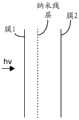
图10示出膜1相对于比较例1的输入光hv的布置;FIG. 10 shows the arrangement of film 1 with respect to the input light hv of Comparative Example 1;
图11示出膜1相对于比较例2的输入光hv的布置;FIG. 11 shows the arrangement of film 1 with respect to the input light hv of Comparative Example 2;
图12示出膜1和膜2相对于比较例3的输入光hv的布置;以及FIG. 12 shows the arrangement of Film 1 and Film 2 with respect to the input light hv of Comparative Example 3; and
图13示出膜1和膜2相对于实施例4的输入光hv的布置。FIG. 13 shows the arrangement of film 1 and film 2 with respect to the input light hv of Example 4. FIG.
这些附图不一定按比例绘制。附图中所使用的相似的数字是指相似的部件。然而,应当理解,在给定附图中使用数字指示部件并非旨在限制另一附图中用相同数字标记的部件。The drawings are not necessarily to scale. Like numbers used in the drawings refer to like parts. It should be understood, however, that the use of numbers in a given figure to designate components is not intended to limit components that are designated by the same numbers in another figure.
具体实施方式Detailed ways
本文所述的一些实施方案涉及光学构造,该光学构造包括两个偏振器层以及布置在偏振器层之间的至少一个光散射和光去偏振层。例如,以下所述的一些实施方案包括反射偏振器层和吸收偏振器层,其中反射偏振器层和吸收性偏振器层之间设置有光学透明导电层,诸如基于纳米线的透明导体层。已发现由各种实施方式举例说明的光学构造表现出比包括反射偏振器、吸收偏振器以及光散射层的其它光学布置低的透射雾度。Some embodiments described herein relate to optical constructions that include two polarizer layers and at least one light scattering and light depolarizing layer disposed between the polarizer layers. For example, some embodiments described below include a reflective polarizer layer and an absorptive polarizer layer with an optically transparent conductive layer, such as a nanowire-based transparent conductor layer, disposed between the reflective polarizer layer and the absorptive polarizer layer. The optical constructions exemplified by the various embodiments have been found to exhibit lower transmission haze than other optical arrangements including reflective polarizers, absorbing polarizers, and light scattering layers.
金属纳米线层和/或其它导电层可表现出光散射,导致具有集成在其中的纳米线层的透明构造的透射雾度增加。对于光学构造的元件诸如液晶显示器,并且根据显示器的详细设计,透射雾度可降低显示器的性能(例如,通过降低对比度来降低液晶显示器的视觉质量)。因此,通过本公开中论述的各种实施方案举例说明的构造允许将一个或多个光学透明导电层(诸如基于金属纳米线的透明导体层)结合到光学构造中,同时通过纳米线或其它导电元件减少光散射的负面影响。Metal nanowire layers and/or other conductive layers may exhibit light scattering, resulting in increased transmission haze of transparent constructs having nanowire layers integrated therein. For optically constructed elements such as liquid crystal displays, and depending on the detailed design of the display, transmission haze can degrade the performance of the display (eg, reduce the visual quality of the liquid crystal display by reducing contrast). Thus, the constructions exemplified by the various embodiments discussed in this disclosure allow for the incorporation of one or more optically transparent conductive layers, such as metal nanowire-based transparent conductor layers, into an optical construction, while conducting electricity through nanowires or other The element reduces the negative effects of light scattering.
当与偏振器层组合时,一个或多个光学透明导电层可在光学构造或设备(例如,液晶显示器)中起到一种或多种功能的作用。这些功能包括但不限于例如电磁干扰屏蔽、静电耗散、感测(例如,触觉感测和/或力感测)以及用于液晶切换的电场的施加。When combined with a polarizer layer, one or more optically transparent conductive layers can serve one or more functions in an optical construction or device (eg, a liquid crystal display). These functions include, but are not limited to, eg, electromagnetic interference shielding, electrostatic dissipation, sensing (eg, tactile sensing and/or force sensing), and application of electric fields for liquid crystal switching.
本文所公开的示例性光学构造可用于偏振膜叠堆、单片偏振片、可切换私密滤光器、电致变色窗、液晶显示模块以及液晶显示器。The exemplary optical constructions disclosed herein can be used in polarizing film stacks, monolithic polarizers, switchable privacy filters, electrochromic windows, liquid crystal display modules, and liquid crystal displays.
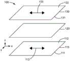
图1示出根据一些实施方案的光学构造100的分解透视图。光学构造100包括具有第一主表面111、相对的第二主表面112以及第一透光轴113的反射偏振器层110。光学构造100布置成使得反射偏振器层110的第一主表面111接收输入光。FIG. 1 shows an exploded perspective view of an
光学构造100还包括具有第一主表面131、相对的第二主表面132以及与反射偏振器层110的第一透光轴基本上对准的第二透光轴133的吸收偏振器层130,其中基本上对准是指轴在约15度内、在一些实施方案中在约10度内、在其它实施方案中在约5度内的平行对准。
在反射偏振器层110和吸收偏振器层130之间布置有至少一个光学透明导电的光散射和光去偏振层120。反射偏振器层110、光散射层120以及吸收偏振器层130布置成基本上平行且重叠。在反射偏振器层110的第一表面111处入射的输入光中的至少一些穿过反射偏振器层110、光散射层120以及吸收偏振器层130,并从吸收偏振器层130的第二表面132离开。At least one optically transparent conductive light scattering and light depolarizing
根据一些实施方案,光散射层120可布置成直接邻近反射偏振器层110的第二表面112,而没有任何中间层。在另选的实施方案中,在光散射层120和反射偏振器层110的第二表面112之间可存在至少一个附加层,例如粘合剂层。根据一些实施方案,光散射层120可布置成直接邻近吸收偏振器层130的第一表面131,而没有任何中间层。在另选的实施方案中,在光散射层120和吸收偏振器层130的第一表面131之间可存在至少一个附加层,例如粘合剂层。根据一些实施方案,光散射层120可布置在与反射偏振器层110和吸收偏振器130隔开的支撑基材上,例如单独的聚合物膜,诸如聚对苯二甲酸乙二醇酯(PET)、聚萘二甲酸乙二醇酯(PEN)、聚碳酸酯(PC)、聚(甲基丙烯酸甲酯)(PMMA)、环烯烃聚合物(COP)、环烯烃共聚物(COC)、三乙酸纤维素(TAC),或它们的共聚物或共混物。According to some embodiments, the
已经发现如本文所公开的光学构造表现出比包括反射偏振器、吸收偏振器以及光散射层(诸如基于纳米线的层)的其它光学构造低的透射雾度。光学构造100的透射雾度可以为在例如约0.1%和10%之间、约0.2%和5%之间、约0.3%和3%之间、约0.4%和2%之间、约0.5%和1.5%之间,或不大于约1.0%。光学构造100的透射雾度小于没有吸收偏振器层的光散射层和反射偏振器层的组合的透射雾度。例如,光学构造100的透射雾度可以比没有吸收偏振器层的光散射层和反射偏振器层的组合的透射雾度小至少约10%、约20%、约30%、约40%,或甚至约50%。Optical constructions as disclosed herein have been found to exhibit lower transmission haze than other optical constructions including reflective polarizers, absorbing polarizers, and light scattering layers, such as nanowire-based layers. The transmission haze of
反射偏振器层110可以是聚合物多层光学膜(MOF)的至少一部分。在一些配置中,反射偏振器层可用任何部分反射器代替,例如可见光反射率在25%和75%之间的部分反射器。吸收偏振器层130可以是聚合物偏振膜的至少一部分。The
光散射层120包括使光散射并去偏振的光学透明导电层。在一些实施方案中,光散射层120可以是基本上连续的无空隙层。另选地,光散射层120可包括空隙。光散射层可设置在支撑基板诸如聚合物膜上。另选地,在一些实施方案中,光散射层可不包括单独的支撑基材,而是可直接被涂覆在至少一个邻近层(例如反射偏振器层和吸收偏振器层中的至少一个)上。The
光散射层120的厚度(沿图1中的z方向)可为任何需要或适于施加的厚度,优选在约1纳米和1微米之间。例如,在各种实施方案中,光散射层120的厚度可为在约5纳米和500纳米之间,或在约10纳米和250纳米之间。光散射层120可具有在约0.1%和10%之间、约0.2%和5%之间、约0.3%和3%之间、约0.4%和2%之间、约0.5%和1.5%之间,或不大于约1.0%的透射雾度。光散射层120的折射率可为大于约1.40且小于约2.20,例如,在约1.45和2.10之间,或约1.50和1.80之间。The thickness of the light scattering layer 120 (in the z direction in FIG. 1 ) can be any desired or suitable thickness for application, preferably between about 1 nanometer and 1 micrometer. For example, in various embodiments, the thickness of
光散射层结合合适的导电材料,该导电材料提供在约0.01欧姆/平方和109欧姆/平方之间的光散射层120的薄层电阻。例如,在各种具体实施中,光散射层120的薄层电阻可在约0.1欧姆/平方至1000欧姆/平方、约1欧姆/平方至100欧姆/平方、约5欧姆/平方至75欧姆/平方,或约10欧姆/平方至60欧姆/平方之间。The light scattering layer incorporates a suitable conductive material that provides a sheet resistance of the
在一些实施方案中,光散射层包括导电纳米线,诸如金属、金属合金和/或导电金属氧化物的纳米线。在一些实施方案中,纳米线可具有约1纳米至100纳米的平均直径,并且平均长度可为约1微米至50微米。在一些实施方案中,纳米线可具有约5纳米至20纳米的平均直径,并且平均长度可为约5微米至10微米。纳米线可嵌入在无孔的、无空隙的聚合物基体中。例如,在各种具体实施中,纳米线的长径比可为大于约5、大于约10、大于约100,或甚至大于约1000。在一些配置中,纳米线在光散射层的平面内可具有随机取向。在一些配置中,纳米线可以以规则图案诸如二维网格(例如,正方形网格)布置。In some embodiments, the light scattering layer includes conductive nanowires, such as nanowires of metals, metal alloys, and/or conductive metal oxides. In some embodiments, the nanowires can have an average diameter of about 1 nanometer to 100 nanometers, and an average length of about 1 micrometer to 50 micrometers. In some embodiments, the nanowires can have an average diameter of about 5 nanometers to 20 nanometers, and an average length of about 5 micrometers to 10 micrometers. Nanowires can be embedded in a non-porous, non-voided polymer matrix. For example, in various implementations, the nanowires can have an aspect ratio greater than about 5, greater than about 10, greater than about 100, or even greater than about 1000. In some configurations, the nanowires can have random orientations within the plane of the light scattering layer. In some configurations, the nanowires can be arranged in a regular pattern, such as a two-dimensional grid (eg, a square grid).
除此之外或另选地,在一些实施方案中,光散射层120可包括碳纳米管,例如,如在共同拥有的美国专利8,384,691中所述的,该专利通过引用并入本文。光散射层120可包括布置成形成导电网孔的导电线,例如金属线。Additionally or alternatively, in some embodiments, the
除此之外或另选地,在一些实施方案中,光散射层120可包括图案化的薄膜金属(例如,银、铝、金、钯)网孔或网格(例如,正方形网格、六边形网孔或随机化网孔)。图案化的薄膜金属网孔可包括宽度例如为在0.05微米和10微米之间、0.1微米和5微米之间或0.2微米和1微米之间的迹线。图案化的薄膜金属网孔的厚度可例如为在0.05微米和10微米之间、在0.1微米和5微米之间,或在0.2微米和1微米之间。Additionally or alternatively, in some embodiments, the
光散射层的导电元件,例如纳米线、碳纳米管等可被支撑在单独的基材(例如聚合物膜)上。导电元件可被涂覆到反射偏振器层和吸收偏振器层中的任一者或两者上。The conductive elements of the light scattering layer, eg, nanowires, carbon nanotubes, etc., may be supported on a separate substrate (eg, a polymer film). The conductive elements can be coated on either or both of the reflective polarizer layer and the absorbing polarizer layer.
在一些实施方案中,光散射层的导电元件(例如纳米线、碳纳米管等)可形成覆盖大部分光散射层120的导电层。在一些实施方案中,导电元件可被图案化以形成导电区域,例如导电线路、电线、迹线或焊盘,以在散射层120内形成一个或多个导电元件。In some embodiments, the conductive elements (eg, nanowires, carbon nanotubes, etc.) of the light scattering layer may form a conductive layer that covers a majority of the
任何或所有前述层都可使用例如光学透明的粘合剂进行光学粘结。任选地,反射偏振器层、吸收偏振器层以及光散射层中的一些或全部三个可被集成到单一的主体中。Any or all of the foregoing layers may be optically bonded using, for example, an optically clear adhesive. Optionally, some or all three of the reflective polarizer layer, the absorbing polarizer layer, and the light scattering layer can be integrated into a single host.
在各种实施方案中,光学构造任选还包括光源,该光源布置成朝向反射偏振器的第一主表面发出光。该光源可以是显示器的背光组件的至少一部分。In various embodiments, the optical construction optionally further includes a light source arranged to emit light toward the first major surface of the reflective polarizer. The light source may be at least part of a backlight assembly of the display.
光学构造任选还包括显示面板,例如可被定位成朝向吸收偏振器的第二主表面的液晶显示面板。The optical construction optionally also includes a display panel, such as a liquid crystal display panel, which may be positioned toward the second major surface of the absorbing polarizer.
图2提供根据一些实施方案的光学构造200的分解透视图。光学构造200包括反射偏振器层210和吸收偏振器层230,这两者间设置有光散射层220。反射偏振器层210具有第一主表面211、相对的第二主表面212以及第一透光轴213。吸收偏振器层230具有第一主表面231、第二主表面232以及与第一透光轴213基本上对准的第二透光轴233。吸收偏振器层230与反射偏振器层210重叠,以在垂直于层210、220、230的平面中限定重叠投影区域209。吸收偏振器层230的第一主表面231取向成朝向反射偏振器层101的第二主表面212。FIG. 2 provides an exploded perspective view of an
光学透明导电的光散射层220(例如,基于金属纳米线的透明导体层)布置成基本上平行于反射偏振器层210和吸收偏振器层230,并且插入在反射偏振器层210的第二主表面212和吸收偏振器层230的第一主表面231之间。光散射层220与反射偏振器层210和吸收偏振器层230的重叠投影区域209重叠。An optically transparent conductive light scattering layer 220 (eg, a metal nanowire-based transparent conductor layer) is arranged substantially parallel to the
光学构造200还包括光源240,该光源240产生被引导朝向反射偏振器层210的第一主表面211的输入光。例如,在一些具体实施中,光源240可以是显示器的背光组件的至少一部分。光学构造200还可包括显示面板250,该显示面板250例如包括被定位成靠近吸收偏振器层230的第二主表面232的一个或多个LCD元件的阵列。光学构造200还可包括附加的偏振器260,例如具有相对于第一透光轴213和第二透光轴233成一定角度(例如,基本上正交)的第三透光轴263的吸收偏振器。
图3是根据一些实施方案的光学构造300的侧视图。光学构造300包括具有第一主表面311、第二主表面312以及第一透光轴313的反射偏振器层310。光学构造300还包括具有第一主表面331、第二主表面332以及与第一透光轴313基本上对准的第二透光轴333的吸收偏振器层330。光学透明导电的光散射层320(例如,基于金属纳米线的透明电导体)被涂覆在反射偏振器层310的第二主表面312上。FIG. 3 is a side view of an
如图3所示,光学构造300可包括光源340,该光源340被定位成使得光源340发出被引导朝向反射偏振器层310的第一主表面311的输入光。例如,光源340可以是显示器的背光组件的部件。显示面板350可被定位成靠近吸收偏振器层330的第二主表面332。如图3所示,在一些实施方案中,光学构造300可以包括靠近显示面板350的一个或多个附加层360,例如沿与吸收偏振器层330相对的显示面板的表面设置的附加吸收偏振器。As shown in FIG. 3 ,
光学透明的粘合剂层可设置在光学构造的成对的邻近层之间。光学构造300包括光学透明的粘合剂层371、372以及373。粘合剂层371设置在光散射层320和吸收偏振器层330的第一主表面331之间,并且用于将光散射层310粘结到吸收偏振器层330。粘合剂层372设置在吸收偏振器层330的第二主表面332和显示模块350之间,并且用于将吸收偏振器层330粘结到显示模块350。粘合剂层373设置在显示模块350和附加偏振器层360之间,并且用于将显示模块350粘结到附加偏振器层360。An optically clear adhesive layer may be disposed between pairs of adjacent layers of the optical construction.
图4是根据一些实施方案的光学构造400的侧视图。光学构造400包括具有第一主表面411、第二主表面412以及第一透光轴413的反射偏振器层410。光学构造400还包括具有第一主表面431、第二主表面432以及与第一透光轴413基本上对准的第二透光轴433的吸收偏振器层430。光学透明导电的光散射层420(例如,基于金属纳米线的透明电导体)被涂覆在吸收偏振器层430的第一主表面431上。FIG. 4 is a side view of an
如图4所示,光学构造400可包括光源440,该光源440被定位成使得其发出被引导朝向反射偏振器层410的第一主表面411的输入光。例如,光源440可以是显示器的背光组件的部件。光学构造400还包括显示面板450,诸如液晶显示元件的阵列,该显示面板450被定位成靠近吸收偏振器层430的第二主表面432。如图4所示,在一些实施方案中,光学构造包括附加层460,该附加层460可包括附加吸收偏振器层。As shown in FIG. 4 , the
光学透明的粘合剂层可设置在光学构造400的成对的邻近层之间。粘合剂层471设置在光散射层420和反射偏振器层410的第二主表面412之间,并且用于将光散射层420粘结到反射偏振器层410。粘合剂层472设置在吸收偏振器层430的第二主表面432和显示面板450之间,并且用于将吸收偏振器层430粘结到显示面板450。粘合剂层473设置在显示面板450和附加偏振器层460之间,并且用于将显示面板450粘结到附加偏振器层460。Optically clear adhesive layers may be disposed between pairs of adjacent layers of
当与本文所述的偏振器层组合时,光学透明导电层(诸如基于纳米线的层)可在光学构造或设备诸如液晶显示器(LCD)中起到一种或多种功能的作用,这些功能包括但不限于电磁干扰屏蔽、静电耗散、感测(例如,基于电阻或电容的触觉感测和/或力感测),以及用于切换液晶显示器中晶体取向的电场的施加。When combined with the polarizer layers described herein, optically transparent conductive layers, such as nanowire-based layers, can serve one or more functions in optical constructions or devices such as liquid crystal displays (LCDs) These include, but are not limited to, electromagnetic interference shielding, electrostatic dissipation, sensing (eg, resistive or capacitive based tactile sensing and/or force sensing), and application of electric fields for switching crystal orientations in liquid crystal displays.
图5是示出根据前述实施方案中任一项的光学构造500的框图,其中光散射层520设置在反射偏振器层510和吸收偏振器层530之间。光散射层520通过一个或多个电连接件598连接,以允许光学构造500结合电路599的操作。根据一个示例实施方案,一个或多个电连接件598被配置为电连接光散射层520以作为触觉传感器和力传感器中的一者或两者进行操作。在该示例中,电路599可包括触觉传感器控制器电路和/或力传感器控制器电路。FIG. 5 is a block diagram illustrating an
一些电容式和/或电阻式触觉传感器和/或力传感器(本文中称为触觉传感器/力传感器)可包括导电线的第一导电层和第二导电层,其中第一层中的导电线以一定角度(例如正交)延伸到第二层中的电线并且在感测节点处与第二层中的电线重叠。在这些具体实施中,第一导电层和第二导电层可设置在反射偏振器和吸收偏振器之间。导电层的导电线电连接到触觉传感器控制器/力传感器控制器。Some capacitive and/or resistive tactile and/or force sensors (referred to herein as tactile sensors/force sensors) may include a first conductive layer and a second conductive layer of conductive lines, wherein the conductive lines in the first layer start with The wires in the second layer extend at an angle (eg, orthogonally) and overlap the wires in the second layer at the sense node. In these implementations, the first conductive layer and the second conductive layer can be disposed between the reflective polarizer and the absorbing polarizer. The conductive lines of the conductive layer are electrically connected to the tactile sensor controller/force sensor controller.
根据另一个实施方案,一个或多个电连接件598被配置为电连接光散射层520而作为用于显示元件切换的控制接触层。在该示例中,电路599可包括显示控制器电路。例如,光学透明导电的光散射层520可包括被配置为电连接到LCD元件的阵列的可独立寻址的接触焊盘的阵列。通过显示控制器599在光散射层520的导电接触焊盘处选择性地施加电压来控制LCD元件的操作。According to another embodiment, one or more
根据另一个实施方案,一个或多个电连接件598被配置为电连接光散射层520而作为静电放电耗散层。在该示例中,一个或多个电连接件598可提供光散射层到地面之间的低阻抗路径。例如,光散射层520可被电连接使得光散射层520的基本上导电的元件处于接地电位,从而提供静电耗散。在该示例中,电路599包括接地连接(例如,大地接地)。According to another embodiment, one or more
根据又一个实施方案,一个或多个电连接件598被配置为电连接光散射层520而作为电磁干扰屏蔽件。在该示例中,一个或多个电连接件可提供到地面的低阻抗路径。例如,光散射层520可被电连接为使得光散射层530的基本上所有的导电元件都处于接地电位,从而提供对电磁干扰的屏蔽。在该示例中,电路599包括接地连接,例如电路接地、底板接地和/或大地接地。According to yet another embodiment, one or more
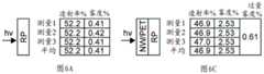
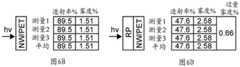
以上参考图5提供的示例示出光学透明导电材料结合偏振器使用提供可用功能的一些方式。透明或发光设备(例如,显示器)的构造的材料的透射雾度(根据ASTM D1003-11)有时可降低设备性能或质量,例如显示器的对比度。发明人意外地认识到,纳米线层与反射偏振器层的组合产生的构造表现出比由纳米线层和反射偏振器层组成部件贡献的雾度的总和明显高的测量雾度。术语“过量雾度”在本文中用于描述多层构造的测量雾度百分比值超出单独组成层的雾度百分比的总和的雾度量(以雾度百分比差表示)。为了说明遇到的问题,图6A至图6D记录包括被涂覆在PET膜上的基于银纳米线的透明导体层(表示为NW/PET)和反射偏振膜(表示为RP)的光学构造的光透射率和雾度测量的结果。图6A至图6D还记录组成层中的每个的光透射率和雾度测量结果。最后,图6A至图6D记录光学构造的雾度和光学构造的组成膜的雾度的总和之间的差(“过量雾度”)。应当理解,这些测量确认光学构造的雾度超过光学构造的组成部件的雾度,导致过量雾度。The examples provided above with reference to FIG. 5 illustrate some of the ways in which the use of optically transparent conductive materials in conjunction with polarizers provides useful functionality. Transmission haze (according to ASTM D1003-11) of materials of construction of transparent or light emitting devices (eg, displays) can sometimes reduce device performance or quality, such as the contrast ratio of displays. The inventors have unexpectedly realized that the combination of the nanowire layer and the reflective polarizer layer produces a construction that exhibits a significantly higher measured haze than the sum of the haze contributed by the nanowire layer and the reflective polarizer layer component parts. The term "excess haze" is used herein to describe the amount of haze (expressed as the difference in percent haze) that measures the percent haze value of a multilayer construction over the sum of the percent haze of the individual constituent layers. To illustrate the problems encountered, Figures 6A-6D record optical constructions comprising a silver nanowire-based transparent conductor layer (denoted NW/PET) and a reflective polarizing film (denoted RP) coated on a PET film Results of light transmittance and haze measurements. Figures 6A-6D also record light transmittance and haze measurements for each of the constituent layers. Finally, Figures 6A-6D record the difference between the haze of the optical construction and the sum of the hazes of the constituent films of the optical construction ("excess haze"). It will be appreciated that these measurements confirm that the haze of the optical construction exceeds the haze of the component parts of the optical construction, resulting in excess haze.
本文所公开的实施方案提供这样的解决方案,该解决方案降低偏振构造的透射雾度,该偏振构造包括光散射层,诸如基于金属纳米线的透明导体层,或其它反射且去偏振的光散射介质。该解决方案利用了本文报道的图6A至图6D中所示的意想不到的过量雾度的来源的新理解。以前未知的过量透射雾度行为的来源已经被理解为至少部分地源于偏振器的部分反射率和基于金属纳米线的透明导体层的非偏振向后散射(或漫反射)之间的相互作用。Embodiments disclosed herein provide solutions that reduce transmission haze of polarized constructs that include light scattering layers, such as metal nanowire-based transparent conductor layers, or other reflective and depolarized light scattering medium. This solution exploits the new understanding of the source of the unexpected excess haze shown in Figures 6A-6D reported herein. The source of the previously unknown excess transmission haze behavior has been understood to arise, at least in part, from the interaction between the partial reflectivity of the polarizer and the unpolarized backscattering (or diffuse reflection) of the metal nanowire-based transparent conductor layer. .
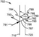
图7和图8示出纳米线层相对于反射偏振器层和入射光的两种可能的布置中的每一种的过量雾度形成的机理。图7和图8示出基于金属纳米线的透明导体层和反射偏振器的组合的过量雾度形成(代表雾度放大)的机理。在图7和图8中所示的概念性示意图中,散射光由虚线指示,相对强度由线的权重指示。图7示出其中输入光入射在纳米线层上的操作。图8示出其中输入光入射在反射偏振器层上的操作。需注意,并非所有散射光都在图7和图8中呈现,相反呈现了对于描述操作和/或较大分量而言更重要的分量。散射光(透射散射光和反射散射光)的净量由具有急剧下降的强度的无限系列的分量给定。Figures 7 and 8 illustrate the mechanism of excess haze formation of the nanowire layer with respect to each of the two possible arrangements of the reflective polarizer layer and incident light. Figures 7 and 8 illustrate the mechanism of excess haze formation (representing haze amplification) for the combination of a metal nanowire-based transparent conductor layer and a reflective polarizer. In the conceptual schematics shown in Figures 7 and 8, scattered light is indicated by dashed lines, and relative intensities are indicated by the weights of the lines. Figure 7 shows the operation in which input light is incident on the nanowire layer. Figure 8 illustrates operation in which input light is incident on the reflective polarizer layer. Note that not all scattered light is presented in Figures 7 and 8, but instead presents components that are more important for describing the operation and/or larger components. The net amount of scattered light (transmitted scattered light and reflected scattered light) is given by an infinite series of components with steeply decreasing intensities.
图7示出具有邻近反射偏振器层710的纳米线层720的光学构造701,其中输入光(由箭头771表示)入射在纳米线层720上。从光学构造701出射的光具有三个分量,该三个分量在图7中被标记为镜面透射(箭头772)、主纳米线(NW)雾度(箭头775)以及过量雾度(箭头779)。在以下的光路径的描述中,将反射偏振器视为理想的反射偏振器(即,沿透光轴偏振的所有光将透射,并且与透光轴正交偏振的所有光将反射)。在实际的反射偏振器中,包括菲涅耳(Fresnel)反射和入射角依赖的其它效应将引起与理想行为的一些偏差,然而该偏差一般较小,并且基本上不改变所述的相互作用。FIG. 7 shows an
输入光的一部分不被纳米线层720散射,并且穿过纳米线层720到反射偏振器710。穿过纳米线层720并且还具有与反射偏振器710的透光轴对准的偏振的未经散射的光穿过反射偏振器710,提供镜面透射分量772。A portion of the input light is not scattered by the
一些输入光被纳米线层720散射,产生反向散射光774和前向散射光770。具有与反射偏振器710的透光轴对准的偏振的前向散射光770穿过反射偏振器710。前向散射的偏振光提供主纳米线雾度775。Some of the input light is scattered by the
未被纳米线层720散射并且不具有与反射偏振器710的透光轴对准的偏振的光被反射偏振器710反射朝向纳米线层720(箭头773)。当该反射光(箭头773)与纳米线层720相互作用时,一些光被纳米线层720前向散射778(相对于光773的方向向前),并且一些光被纳米线层720反向散射787(相对于光773的方向向后)。被纳米线层720反向散射并且还具有与反射偏振器710的透光轴对准的偏振的光787穿过反射偏振器。这种偏振器反射的、然后纳米线反向散射的并且然后偏振的光779提供光学构造701的过量雾度中的至少一些。Light that is not scattered by the
图8示出具有邻近反射偏振器710的纳米线层720的光学构造702,其中输入光781入射在反射偏振器710上。从光学构造702出射的光具有三个分量,该三个分量在图8中被标记为镜面透射782、主纳米线(NW)雾度785以及过量雾度788、789。FIG. 8 shows an
一些输入光781具有与反射偏振器710的透光轴对准的偏振,并且穿过反射偏振器到纳米线层720(箭头787)。未被纳米线层720散射的光提供镜面透射782。穿过反射偏振器710即被纳米线层720前向散射的光提供主NW雾度785。不具有与反射偏振器710的透光轴对准的偏振的光被反射偏振器反射(箭头783)。Some of the
穿过反射偏振器720的一些光被纳米线层720反向散射朝向反射偏振器720(箭头786)。具有与反射偏振器710的透光轴对准的偏振的反向散射光可穿过反射偏振器710(箭头784)。具有不与反射偏振器710的透光轴对准的偏振的反向散射光被反射偏振器710反射(箭头780)。该反射的偏振光780中的一些穿过纳米线层720而不被散射而作为过量雾度分量789。反向散射并且然后反射的光780中的一些被纳米线层720前向散射而作为过量雾度分量788。Some of the light passing through
借助于上述对雾度放大的来源的理解,并且为了降低光散射层和偏振器组合的雾度,开发了如本文提供的实施方案中所论述的新设计。如示例性实施方案中所示,新设计实施方案涉及在透光轴对准的反射偏振器和吸收偏振器之间插入基于金属纳米线的透明导体层(或其它导电的光散射介质),以获得偏振选择光再循环。With the above understanding of the source of haze amplification, and in order to reduce the haze of the light scattering layer and polarizer combination, a new design as discussed in the embodiments provided herein was developed. As shown in the exemplary embodiment, the new design embodiment involves inserting a metal nanowire-based transparent conductor layer (or other conductive light scattering medium) between the reflective polarizer and the absorbing polarizer that are aligned with the transmission axis, to Obtain polarization-selective light recycling.
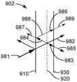
图9A示意性地示出比较光学构造901的操作,该比较光学构造包括从光源按以下次序布置的透明导电纳米线层、反射偏振器层以及吸收偏振器层。比较构造901导致相对高的雾度。图9B示意性地示出根据本文所论述的实施方案的光学构造902的操作,其提供过量雾度降低的机理。在光学构造902中,透明导电纳米线层920设置在反射偏振器层910和吸收偏振器层930之间,其中来自光源的输入光入射在反射偏振器层910上。在构造901和构造902中,反射偏振器的透光轴平行于吸收偏振器的透光轴。Figure 9A schematically illustrates the operation of a comparative
图9A示出其中输入光(由箭头971表示)入射在纳米线层920上的构造901。从光学构造901出射的光具有三个分量,该三个分量在图9A中被标记为镜面透射(箭头972)、主纳米线(NW)雾度(箭头975)以及过量雾度(箭头979)。FIG. 9A shows a
输入光的一部分不被纳米线层920散射,并且穿过纳米线层920到反射偏振器910。穿过纳米线层920并且还具有与反射偏振器910的透光轴和吸收偏振器930的透光轴对准的偏振的未经散射的光穿过反射偏振器920和吸收偏振器930,提供镜面透射分量972。A portion of the input light is not scattered by
一些输入光被纳米线层920散射,产生反向散射光974和前向散射光970。具有与反射偏振器910的透光轴和吸收偏振器930的透光轴对准的偏振的前向散射光970的一部分穿过反射偏振器层910和吸收偏振器层930。前向散射的偏振光提供主纳米线雾度975。Some of the input light is scattered by the
未被纳米线层920散射并且不具有与反射偏振器910的透光轴对准的偏振的光973被反射偏振器910反射朝向纳米线层920。当反射光973与纳米线层920相互作用时,一些光被纳米线层920前向散射978(相对于光973向前),并且一些光被纳米线层920反向散射977(相对于光973向后)。被纳米线层920反向散射并且还具有与反射偏振器910和吸收偏振器930的透光轴对准的透光轴的光977穿过反射偏振器910和吸收偏振器930。该反射的、反向散射的并且偏振的光979提供光学构造901的过量雾度中的至少一些。在比较光学构造901中,由于反射偏振器和吸收偏振器的透光轴的对准,穿过反射偏振器910的光也将穿过吸收偏振器。输出光分量979、972、975被偏振到吸收偏振器930的透光轴,导致相对高的雾度。
图9B示意性地示出光学构造902的操作,该光学构造具有设置在反射偏振器910和吸收偏振器930之间的纳米线层920,其中输入光981入射在反射偏振器910上。从光学构造902出射的光具有三个分量,该三个分量在图9B中被标记为镜面透射982、主纳米线(NW)雾度985以及过量雾度989。9B schematically illustrates the operation of an
具有与反射偏振器910的透光轴对准的偏振的输入光穿过反射偏振器910到纳米线层920。光散射纳米线层920使从反射偏振器910出射的一些光散射并去偏振。穿过反射偏振器910的一些光983被前向散射朝向吸收偏振器。具有与吸收偏振器的透光轴对准的偏振的前向散射光穿过吸收偏振器而作为主NW雾度985。从纳米线层反向散射(箭头984)并且具有与反射偏振器的透光轴对准的偏振的光离开构造902(箭头987)。只有具有与反射偏振器的透光轴正交的偏振的光被反射偏振器910反射朝向纳米线层920(箭头988)。当光988遇到纳米线层920时,光988的大部分穿过纳米线层并且保持偏振(其中偏振与反射偏振器的透光轴正交),并且少数部分被前向散射并去偏振(多数部分和少数部分都被示为箭头986)。在从纳米线层920出射的光986中,只有具有与吸收偏振器的透光轴对准的偏振的分量(光986的少数分量的一部分)才能作为过量雾度989穿过吸收偏振器,并且光986的剩余部分(多数分量)被吸收(从而降低过量雾度)。在构造902中,只有镜面透射982分量完全穿过吸收偏振器。因为插入在反射偏振器910和吸收偏振器930之间的纳米线层920使从反射偏振器910出射的前向散射光去偏振,所以至少部分地降低了主雾度。因为从纳米线层向后散射的具有与吸收偏振器的透光轴对准的偏振的光通过反射偏振器向后离开,并且不对雾度做出贡献,所以过量雾度被大大衰减。被纳米线层前向散射并具有与吸收偏振器的透光轴不同的偏振的光被吸收偏振器衰减,导致主雾度和过量雾度降低。Input light with polarization aligned with the transmission axis of
实施例Example
通过堆叠单独的膜来制备膜组件(光学构造)。测量膜组件的透射雾度(Suga HazeMeter HZ-V3(Suga雾度计HZ-V3),日本东京的须贺测试仪器公司(Suga TestInstruments,Tokyo,Japan))。比较例1至比较例3和实施例4的结果记录在表1中。比较例5至比较例7和实施例8的结果记录在表2中。这些结果确认,包括设置在反射偏振器和吸收偏振器之间的纳米线层的光学构造在与包括纳米线层和反射偏振器(没有吸收偏振器)的比较光学构造相比时,表现出降低的雾度,并且在与包括纳米线层、反射偏振器以及吸收偏振器的比较光学构造(其中反射偏振器位于纳米线层和吸收偏振器之间)相比时,表现出降低的雾度。Film assemblies (optical constructions) are prepared by stacking individual films. The transmission haze of the membrane assembly was measured (Suga HazeMeter HZ-V3 (Suga Haze Meter HZ-V3), Suga Test Instruments, Tokyo, Japan). The results of Comparative Examples 1 to 3 and Example 4 are reported in Table 1. The results of Comparative Examples 5 to 7 and Example 8 are reported in Table 2. These results confirm that an optical construction that includes a nanowire layer disposed between a reflective polarizer and an absorbing polarizer exhibits reduced performance when compared to a comparative optical construction that includes a nanowire layer and a reflective polarizer (without the absorbing polarizer) and exhibited reduced haze when compared to a comparative optical configuration including a nanowire layer, a reflective polarizer, and an absorbing polarizer, where the reflective polarizer was located between the nanowire layer and the absorbing polarizer.
膜1(具有银纳米线层涂层的反射偏振器):在侧面A上涂覆有银纳米线(可以商品名
膜2(具有银纳米线层涂层的反射偏振器):在侧面A上涂覆有银纳米线(可以商品名
膜3(吸收偏振器):Sanritz吸收偏振膜(Sanritz HLC2-56-18S,加利福尼亚州丘拉维斯的美国三立子公司(Sanritz America,Chula Vista,California))。膜3包括吸收偏振器层。Film 3 (absorbing polarizer): Sanritz absorbing polarizing film (Sanritz HLC2-56-18S, Sanritz America, Chula Vista, California). Film 3 includes an absorbing polarizer layer.
比较例1:Comparative Example 1 :
使用Suga Haze Meter(Suga雾度计)测量膜1的光透射率和雾度,其中侧面A(纳米线涂覆的侧面)面向光源。图10示出膜1相对于输入光hv的布置。The light transmittance and haze of Film 1 were measured using a Suga Haze Meter, with side A (nanowire-coated side) facing the light source. Figure 10 shows the arrangement of the film 1 with respect to the input light hv.
比较例2:Comparative Example 2 :
使用Suga Haze Meter(Suga雾度计)测量膜1的光透射率和雾度,其中侧面A(纳米线涂覆的侧面)背向光源(即,朝向仪器检测器)。图11示出膜1相对于输入光hv的布置。The light transmittance and haze of Film 1 were measured using a Suga Haze Meter, with side A (the side coated by the nanowires) facing away from the light source (ie, towards the instrument detector). Figure 11 shows the arrangement of the film 1 with respect to the input light hv.
比较例3Comparative Example 3
使用Suga Haze Meter(Suga雾度计)测量包括堆叠的膜1和膜2的膜组件的光透射率和雾度,其中膜1朝向光源(相对于膜2)并且膜1的侧面A面向光源。图12示出膜1和膜2相对于输入光hv的布置。The light transmittance and haze of a film assembly comprising stacked Film 1 and Film 2 with Film 1 facing the light source (relative to Film 2) and side A of Film 1 facing the light source were measured using a Suga Haze Meter. Figure 12 shows the arrangement of film 1 and film 2 with respect to input light hv.
实施例4Example 4
使用Suga Haze Meter(Suga雾度计)测量包括堆叠的膜1和膜2的膜组件,其中膜1朝向光源(相对于膜2)并且膜1的侧面A背向光源(即,朝向膜2)。图13示出膜1和膜2相对于输入光hv的布置。A film assembly comprising stacked film 1 and film 2 was measured using the Suga Haze Meter, with film 1 facing the light source (relative to film 2) and side A of film 1 facing away from the light source (ie, toward film 2) . Figure 13 shows the arrangement of film 1 and film 2 with respect to input light hv.
表1:结果Table 1: Results

比较例5:Comparative Example 5:
使用Suga Haze Meter(Suga雾度计)测量膜2的光透射率和雾度,其中侧面A(纳米线涂覆的侧面)面向光源。The light transmittance and haze of Film 2 were measured using a Suga Haze Meter, with side A (nanowire-coated side) facing the light source.
比较例6:Comparative Example 6:
使用Suga Haze Meter(Suga雾度计)测量膜2的光透射率和雾度,其中侧面A(纳米线涂覆的侧面)背向光源(即,朝向仪器检测器)。Film 2 was measured for light transmittance and haze using a Suga Haze Meter, with side A (the side coated by the nanowires) facing away from the light source (ie, toward the instrument detector).
比较例7:Comparative Example 7:
使用SugaHaze Meter(Suga雾度计)测量包括堆叠的膜2和膜3的膜组件的光透射率和雾度,其中膜2朝向光源(相对于膜3)并且膜2的侧面A面向光源。The light transmittance and haze of the film assembly comprising the stacked film 2 and film 3, with film 2 facing the light source (relative to film 3) and with side A of film 2 facing the light source, were measured using a SugaHaze Meter.
实施例8:Example 8 :
使用SugaHaze Meter(Suga雾度计)测量包括堆叠的膜2和膜3的膜组件的光透射率和雾度,其中膜2朝向光源(相对于膜3)并且膜2的侧面A背向光源(即,朝向膜3)。The light transmittance and haze of the film assembly comprising the stacked film 2 and film 3 were measured using a SugaHaze Meter, with film 2 facing the light source (relative to film 3) and side A of film 2 facing away from the light source ( That is, towards the membrane 3).
表2:结果Table 2: Results

本文所论述的项目包括:Items discussed in this article include:
项目1.一种光学构造,包括:Item 1. An optical construction comprising:
反射偏振器层,该反射偏振器层具有第一透光轴;a reflective polarizer layer having a first transmission axis;
吸收偏振器层,该吸收偏振器层具有与第一透光轴基本上对准的第二透光轴;和an absorbing polarizer layer having a second transmission axis substantially aligned with the first transmission axis; and
至少一个导电的光散射层,该至少一个导电的光散射层位于反射偏振器层和吸收偏振器层之间。At least one conductive light scattering layer located between the reflective polarizer layer and the absorbing polarizer layer.
项目2.根据项目1所述的光学构造,其中光散射层包括金属纳米线。Item 2. The optical construction of item 1, wherein the light scattering layer comprises metallic nanowires.
项目3.根据项目2所述的光学构造,其中金属纳米线嵌入在无孔的聚合物基体中。Item 3. The optical construction of item 2, wherein the metal nanowires are embedded in a non-porous polymer matrix.
项目4.根据项目2所述的光学构造,其中金属纳米线具有大于约5的长径比。Item 4. The optical construction of item 2, wherein the metal nanowires have an aspect ratio greater than about 5.
项目5.根据项目1至项目4中任一项所述的光学构造,其中光散射层包括碳纳米管。Item 5. The optical construction of any one of items 1 to 4, wherein the light scattering layer comprises carbon nanotubes.
项目6.根据项目1至项目4中任一项所述的光学构造,其中光散射层包括图案化的薄膜金属网孔。Item 6. The optical construction of any one of items 1 to 4, wherein the light scattering layer comprises a patterned thin film metal mesh.
项目7.根据项目1至项目6中任一项所述的光学构造,其中光散射层具有介于约0.01欧姆/平方和109欧姆/平方之间的薄层电阻。Item 7. The optical construction of any one of items 1 to 6, wherein the light scattering layer has a sheet resistance between about 0.01 ohms/square and109 ohms/square.
项目8.根据项目1至项目7中任一项所述的光学构造,其中光散射层具有介于约0.2%和5%之间的透射雾度。Item 8. The optical construction of any one of items 1 to 7, wherein the light scattering layer has a transmission haze of between about 0.2% and 5%.
项目9.根据项目1至项目8中任一项所述的光学构造,其中光学构造具有介于约0.1%和10%之间的透射雾度。Item 9. The optical construction of any one of items 1 to 8, wherein the optical construction has a transmission haze of between about 0.1% and 10%.
项目10.根据项目1至项目9中任一项所述的光学构造,其中光学构造的透射雾度小于光散射层和反射偏振器层的组合的透射雾度。Item 10. The optical construction of any one of items 1 to 9, wherein the transmission haze of the optical construction is less than the transmission haze of the combination of the light scattering layer and the reflective polarizer layer.
项目11.根据项目1至项目10中任一项所述的光学构造,其中光散射层具有介于约1纳米和1微米之间的厚度。Item 11. The optical construction of any one of items 1 to 10, wherein the light scattering layer has a thickness of between about 1 nanometer and 1 micrometer.
项目12.根据项目1至项目11中任一项所述的光学构造,其中光散射层具有介于大于约1.40且小于约2.20的折射率。Item 12. The optical construction of any one of items 1 to 11, wherein the light scattering layer has an index of refraction between greater than about 1.40 and less than about 2.20.
项目13.根据项目1至项目12中任一项所述的光学构造,其中反射偏振器包括多层光学膜。Item 13. The optical construction of any one of items 1 to 12, wherein the reflective polarizer comprises a multilayer optical film.
项目14.根据项目1至项目13中任一项所述的光学构造,其中光散射层设置在支撑基材上。Item 14. The optical construction of any one of items 1 to 13, wherein the light scattering layer is disposed on the support substrate.
项目15.根据项目14所述的光学构造,其中支撑基材为聚合物膜。Item 15. The optical construction of item 14, wherein the support substrate is a polymeric film.
项目16.根据项目1至项目15中任一项所述的光学构造,其中光散射层被涂覆在反射偏振器层和吸收偏振器层中的至少一者上。Item 16. The optical construction of any one of items 1 to 15, wherein the light scattering layer is coated on at least one of the reflective polarizer layer and the absorbing polarizer layer.
项目17.根据项目1至项目16中任一项所述的光学构造,其中在反射偏振器层和光散射层之间布置有光学透明的粘合剂层。Item 17. The optical construction of any one of items 1 to 16, wherein an optically clear adhesive layer is disposed between the reflective polarizer layer and the light scattering layer.
项目18.根据项目1至项目17中任一项所述的光学构造,其中在吸收偏振器层和光散射层之间布置有光学透明的粘合剂层。Item 18. The optical construction of any one of items 1 to 17, wherein an optically clear adhesive layer is disposed between the absorbing polarizer layer and the light scattering layer.
项目19.根据项目1至项目18中任一项所述的光学构造,其中:Item 19. The optical construction of any one of items 1 to 18, wherein:
反射偏振器层具有第一主表面和面向光散射层的第二主表面;并且the reflective polarizer layer has a first major surface and a second major surface facing the light scattering layer; and
还包括被配置为将输入光提供给第一主表面的光源。Also included is a light source configured to provide input light to the first major surface.
项目20.根据项目19所述的光学构造,其中:Item 20. The optical construction of item 19, wherein:
吸收偏振器层具有第一主表面和面向光散射层的第二主表面;并且the absorbing polarizer layer has a first major surface and a second major surface facing the light scattering layer; and
还包括与吸收偏振器层的第一主表面相邻的显示模块。Also included is a display module adjacent the first major surface of the absorbing polarizer layer.
项目21.根据项目20所述的光学构造,还包括到光散射层的一个或多个电连接件。Item 21. The optical construction of item 20, further comprising one or more electrical connections to the light scattering layer.
项目22.根据项目21所述的光学构造,其中一个或多个电连接件被配置为电连接光散射层以作为触觉传感器和力传感器中的一者或两者进行操作。Item 22. The optical construction of item 21, wherein the one or more electrical connections are configured to electrically connect the light scattering layer to operate as one or both of a tactile sensor and a force sensor.
项目23.根据项目21所述的光学构造,其中一个或多个电连接件被配置为电连接光散射层而作为电磁干扰屏蔽件。Item 23. The optical construction of item 21, wherein the one or more electrical connections are configured to electrically connect the light scattering layer as an electromagnetic interference shield.
项目24.根据项目21所述的光学构造,其中一个或多个电连接件被配置为电连接光散射层而作为静电放电耗散层。Item 24. The optical construction of item 21, wherein the one or more electrical connectors are configured to electrically connect the light scattering layer as an electrostatic discharge dissipative layer.
项目25.根据项目21所述的光学构造,其中一个或多个电连接件被配置为电连接光散射层而作为用于显示元件切换的控制接触层。Item 25. The optical construction of item 21, wherein the one or more electrical connectors are configured to electrically connect the light scattering layer as a control contact layer for display element switching.
项目26.根据项目21所述的光学构造,其中一个或多个电连接件被配置为通过到地面的低阻抗路径来连接光散射层。Item 26. The optical construction of item 21, wherein the one or more electrical connections are configured to connect the light scattering layer through a low impedance path to ground.
项目27.根据项目1至项目26中任一项所述的光学构造,其中光散射层包括基本上连续的无空隙层。Item 27. The optical construction of any one of items 1 to 26, wherein the light scattering layer comprises a substantially continuous void-free layer.
项目28.一种光学构造,包括:Item 28. An optical construction comprising:
部分反射层,该部分反射层被配置为接收输入光;a partially reflective layer configured to receive input light;
吸收偏振器层;和an absorbing polarizer layer; and
导电的光散射层,该导电的光散射层位于部分反射层和吸收偏振A conductive light-scattering layer that sits on top of the partially reflective layer and absorbs polarization
器层之间。between the layers.
除非另外指明,否则说明书和权利要求书中所使用的所有表达特征尺寸、量和物理特性的数字在所有情况下均应理解为由术语“约”修饰。因此,除非有相反的说明,否则在上述说明书和所附权利要求中列出的数值参数均为近似值,这些近似值可根据本领域的技术人员利用本文所公开的教导内容来寻求获得的期望性能而变化。所使用的由端值表述的数值范围包括此范围内包含的所有数值(例如,1至5包括1、1.5、2、2.75、3、3.80、4和5)以及在此范围内的任何范围。All numbers expressing characteristic dimensions, quantities and physical properties used in the specification and claims should in all instances be understood to be modified by the term "about" unless otherwise indicated. Accordingly, unless indicated to the contrary, the numerical parameters set forth in the foregoing specification and attached claims are approximations that can be derived from the desired properties sought to be obtained by those skilled in the art utilizing the teachings disclosed herein. Variety. The use of numerical ranges by endpoints includes all numbers subsumed within that range (eg, 1 to 5 includes 1, 1.5, 2, 2.75, 3, 3.80, 4, and 5) and any range within that range.
以上论述的实施方案的各种变型和更改对于本领域中的技术人员都是显而易见的,并且应当理解,本公开不限于本文所阐述的示例性实施方案。除非另外指明,否则读者应该假设一个所公开的实施方案的特征也可应用于所有其它所公开的实施方案。应该理解,本文所引用的所有美国专利、专利申请、专利申请公开以及其它专利和非专利文档都以其不与上述公开抵触的程度通过引用的方式并入。Various modifications and alterations to the above-discussed embodiments will be apparent to those skilled in the art, and it should be understood that the present disclosure is not limited to the exemplary embodiments set forth herein. Unless otherwise indicated, the reader should assume that features of one disclosed embodiment are also applicable to all other disclosed embodiments. It should be understood that all US patents, patent applications, patent application publications, and other patent and non-patent documents cited herein are incorporated by reference to the extent that they do not contradict the foregoing disclosure.
Claims (7)
Translated fromChineseApplications Claiming Priority (3)
| Application Number | Priority Date | Filing Date | Title |
|---|---|---|---|
| US201562168205P | 2015-05-29 | 2015-05-29 | |
| US62/168,205 | 2015-05-29 | ||
| PCT/US2016/032677WO2016195981A1 (en) | 2015-05-29 | 2016-05-16 | Optical constructions |
Publications (2)
| Publication Number | Publication Date |
|---|---|
| CN107750347A CN107750347A (en) | 2018-03-02 |
| CN107750347Btrue CN107750347B (en) | 2020-12-29 |
Family
ID=57441441
Family Applications (1)
| Application Number | Title | Priority Date | Filing Date |
|---|---|---|---|
| CN201680031452.3AActiveCN107750347B (en) | 2015-05-29 | 2016-05-16 | Optical construction |
Country Status (4)
| Country | Link |
|---|---|
| US (2) | US10317594B2 (en) |
| CN (1) | CN107750347B (en) |
| TW (1) | TW201730592A (en) |
| WO (1) | WO2016195981A1 (en) |
Families Citing this family (6)
| Publication number | Priority date | Publication date | Assignee | Title |
|---|---|---|---|---|
| EP3350630A1 (en) | 2015-09-16 | 2018-07-25 | 3M Innovative Properties Company | Overcoated patterned conductive layer and methods |
| KR20190007942A (en)* | 2017-07-14 | 2019-01-23 | 코닝 인코포레이티드 | Method of patterning multi-layer structure |
| US11315982B2 (en)* | 2018-12-05 | 2022-04-26 | Boe Technology Group Co., Ltd. | Light emitting diode with a patterned scattering layer and fabrication method thereof, display substrate and display panel |
| CN110989218A (en)* | 2019-11-20 | 2020-04-10 | Tcl华星光电技术有限公司 | Device and method for detecting light leakage of metal signal line |
| CN112432308B (en)* | 2020-11-20 | 2022-07-08 | 珠海格力电器股份有限公司 | Touch interaction device, control method and device thereof and air conditioning unit |
| JP7555856B2 (en)* | 2021-03-05 | 2024-09-25 | Toppanホールディングス株式会社 | Optical member and liquid crystal display device |
Citations (3)
| Publication number | Priority date | Publication date | Assignee | Title |
|---|---|---|---|---|
| CN1236114A (en)* | 1998-04-30 | 1999-11-24 | 精工爱普生株式会社 | Liquid crystal device and electronic device using the liquid crystal device |
| CN101578553A (en)* | 2006-08-29 | 2009-11-11 | 西里厄斯材料股份有限公司 | Windows with electrically controllable transmission and reflection |
| CN101971354A (en)* | 2007-04-20 | 2011-02-09 | 凯博瑞奥斯技术公司 | High contrast transparent conductors and methods of forming the same |
Family Cites Families (17)
| Publication number | Priority date | Publication date | Assignee | Title |
|---|---|---|---|---|
| US6025897A (en)* | 1993-12-21 | 2000-02-15 | 3M Innovative Properties Co. | Display with reflective polarizer and randomizing cavity |
| US6088067A (en)* | 1995-06-26 | 2000-07-11 | 3M Innovative Properties Company | Liquid crystal display projection system using multilayer optical film polarizers |
| JP3935936B2 (en)* | 1995-06-26 | 2007-06-27 | スリーエム カンパニー | Transflective display with reflective polarizing transflective reflector |
| US6538714B1 (en)* | 1999-10-25 | 2003-03-25 | 3M Innovative Properties Company | Dual color guest-host polarizers and devices containing guest-host polarizers |
| JP4207398B2 (en) | 2001-05-21 | 2009-01-14 | 富士ゼロックス株式会社 | Method for manufacturing wiring of carbon nanotube structure, wiring of carbon nanotube structure, and carbon nanotube device using the same |
| US20060257638A1 (en) | 2003-01-30 | 2006-11-16 | Glatkowski Paul J | Articles with dispersed conductive coatings |
| US6900458B2 (en)* | 2003-02-21 | 2005-05-31 | Universal Display Corporation | Transflective display having an OLED backlight |
| TWI403761B (en)* | 2005-02-15 | 2013-08-01 | Fujifilm Corp | Process of producing light transmittancy electroconductibility film |
| US20130002994A1 (en)* | 2005-05-23 | 2013-01-03 | Ran-Hong Raymond Wang | Integrating emi shiel in liquid crystal display devices |
| GB2437553A (en)* | 2006-04-28 | 2007-10-31 | Sharp Kk | Optical system with two spaced apart partial reflectors for display |
| EP2082436B1 (en)* | 2006-10-12 | 2019-08-28 | Cambrios Film Solutions Corporation | Nanowire-based transparent conductors and method of making them |
| US7826009B2 (en) | 2006-12-21 | 2010-11-02 | 3M Innovative Properties Company | Hybrid polarizer |
| US7864270B2 (en)* | 2008-02-08 | 2011-01-04 | Motorola, Inc. | Electronic device and LC shutter with diffusive reflective polarizer |
| KR101720919B1 (en) | 2008-02-28 | 2017-03-28 | 쓰리엠 이노베이티브 프로퍼티즈 컴파니 | Touch screen sensor |
| US20100117988A1 (en)* | 2008-11-12 | 2010-05-13 | Adrian Marc Simon Jacobs | Optical element and touch sensor |
| KR101029287B1 (en)* | 2008-12-03 | 2011-04-18 | 하이디스 테크놀로지 주식회사 | LCD with Touch Screen |
| US10042201B2 (en)* | 2014-12-03 | 2018-08-07 | Sharp Kabushiki Kaisha | Liquid crystal display device |
- 2016
- 2016-05-16USUS15/568,016patent/US10317594B2/ennot_activeExpired - Fee Related
- 2016-05-16CNCN201680031452.3Apatent/CN107750347B/enactiveActive
- 2016-05-16WOPCT/US2016/032677patent/WO2016195981A1/ennot_activeCeased
- 2016-05-27TWTW105116743Apatent/TW201730592A/enunknown
- 2019
- 2019-05-22USUS16/419,339patent/US12099223B2/enactiveActive
Patent Citations (3)
| Publication number | Priority date | Publication date | Assignee | Title |
|---|---|---|---|---|
| CN1236114A (en)* | 1998-04-30 | 1999-11-24 | 精工爱普生株式会社 | Liquid crystal device and electronic device using the liquid crystal device |
| CN101578553A (en)* | 2006-08-29 | 2009-11-11 | 西里厄斯材料股份有限公司 | Windows with electrically controllable transmission and reflection |
| CN101971354A (en)* | 2007-04-20 | 2011-02-09 | 凯博瑞奥斯技术公司 | High contrast transparent conductors and methods of forming the same |
Also Published As
| Publication number | Publication date |
|---|---|
| TW201730592A (en) | 2017-09-01 |
| WO2016195981A1 (en) | 2016-12-08 |
| US20190278009A1 (en) | 2019-09-12 |
| CN107750347A (en) | 2018-03-02 |
| US12099223B2 (en) | 2024-09-24 |
| US20180143360A1 (en) | 2018-05-24 |
| US10317594B2 (en) | 2019-06-11 |
Similar Documents
| Publication | Publication Date | Title |
|---|---|---|
| CN107750347B (en) | Optical construction | |
| CN103109213B (en) | Light diffusion element, the polarization plates of band light diffusion element, polarization element and use its liquid crystal indicator | |
| CN105761623B (en) | display device | |
| TWI684029B (en) | Polarized light source device | |
| JP6126016B2 (en) | Optical film laminate | |
| US20190220151A1 (en) | Laminate for touch panel, flexible device, and organic electroluminescence display device | |
| CN106105389B (en) | EL element, EL element substrate, lighting device, display equipment and LCD device | |
| CN108139624A (en) | Liquid crystal display device | |
| JP7387589B2 (en) | Light control film and liquid crystal display device | |
| KR101443689B1 (en) | Touch sensing electrode combined with polarization plate | |
| JP6243344B2 (en) | Optical stack with asymmetric diffuser | |
| JP2014235397A (en) | Liquid crystal display device | |
| JP2015108827A (en) | Polarization plate for liquid crystal display | |
| JP2016109994A (en) | Liquid crystal display device | |
| CN110596934A (en) | Liquid crystal display panel and driving method | |
| CN105765510A (en) | Hybrid touch sensing electrode and touch screen panel | |
| JP2020129055A (en) | View angle control film, backlight unit, and liquid crystal display device | |
| CN112088330A (en) | Liquid crystal display device having a plurality of pixel electrodes | |
| KR20200054074A (en) | Substrate with transparent electrode layer, light modulation film and liquid crystal display device | |
| KR20200054072A (en) | Substrate with transparent electrode layer, light modulation film and liquid crystal display device | |
| WO2019097930A1 (en) | Optical member | |
| KR102497657B1 (en) | Display device | |
| WO2022214944A1 (en) | Backlight and display system | |
| JP7361683B2 (en) | liquid crystal display device | |
| JP2022133016A (en) | Under display camera type display device |
Legal Events
| Date | Code | Title | Description |
|---|---|---|---|
| PB01 | Publication | ||
| PB01 | Publication | ||
| SE01 | Entry into force of request for substantive examination | ||
| SE01 | Entry into force of request for substantive examination | ||
| GR01 | Patent grant | ||
| GR01 | Patent grant |