CN107680975B - Manufacturing method of display panel, display panel and display device - Google Patents
Manufacturing method of display panel, display panel and display deviceDownload PDFInfo
- Publication number
- CN107680975B CN107680975BCN201710876367.3ACN201710876367ACN107680975BCN 107680975 BCN107680975 BCN 107680975BCN 201710876367 ACN201710876367 ACN 201710876367ACN 107680975 BCN107680975 BCN 107680975B
- Authority
- CN
- China
- Prior art keywords
- pattern
- common electrode
- insulating layer
- electrode pattern
- forming
- Prior art date
- Legal status (The legal status is an assumption and is not a legal conclusion. Google has not performed a legal analysis and makes no representation as to the accuracy of the status listed.)
- Active
Links
Images


Classifications
- H—ELECTRICITY
- H10—SEMICONDUCTOR DEVICES; ELECTRIC SOLID-STATE DEVICES NOT OTHERWISE PROVIDED FOR
- H10D—INORGANIC ELECTRIC SEMICONDUCTOR DEVICES
- H10D86/00—Integrated devices formed in or on insulating or conducting substrates, e.g. formed in silicon-on-insulator [SOI] substrates or on stainless steel or glass substrates
- H10D86/40—Integrated devices formed in or on insulating or conducting substrates, e.g. formed in silicon-on-insulator [SOI] substrates or on stainless steel or glass substrates characterised by multiple TFTs
- H10D86/441—Interconnections, e.g. scanning lines
- G—PHYSICS
- G02—OPTICS
- G02F—OPTICAL DEVICES OR ARRANGEMENTS FOR THE CONTROL OF LIGHT BY MODIFICATION OF THE OPTICAL PROPERTIES OF THE MEDIA OF THE ELEMENTS INVOLVED THEREIN; NON-LINEAR OPTICS; FREQUENCY-CHANGING OF LIGHT; OPTICAL LOGIC ELEMENTS; OPTICAL ANALOGUE/DIGITAL CONVERTERS
- G02F1/00—Devices or arrangements for the control of the intensity, colour, phase, polarisation or direction of light arriving from an independent light source, e.g. switching, gating or modulating; Non-linear optics
- G02F1/01—Devices or arrangements for the control of the intensity, colour, phase, polarisation or direction of light arriving from an independent light source, e.g. switching, gating or modulating; Non-linear optics for the control of the intensity, phase, polarisation or colour
- G02F1/13—Devices or arrangements for the control of the intensity, colour, phase, polarisation or direction of light arriving from an independent light source, e.g. switching, gating or modulating; Non-linear optics for the control of the intensity, phase, polarisation or colour based on liquid crystals, e.g. single liquid crystal display cells
- G02F1/133—Constructional arrangements; Operation of liquid crystal cells; Circuit arrangements
- G02F1/1333—Constructional arrangements; Manufacturing methods
- G02F1/133345—Insulating layers
- G—PHYSICS
- G02—OPTICS
- G02F—OPTICAL DEVICES OR ARRANGEMENTS FOR THE CONTROL OF LIGHT BY MODIFICATION OF THE OPTICAL PROPERTIES OF THE MEDIA OF THE ELEMENTS INVOLVED THEREIN; NON-LINEAR OPTICS; FREQUENCY-CHANGING OF LIGHT; OPTICAL LOGIC ELEMENTS; OPTICAL ANALOGUE/DIGITAL CONVERTERS
- G02F1/00—Devices or arrangements for the control of the intensity, colour, phase, polarisation or direction of light arriving from an independent light source, e.g. switching, gating or modulating; Non-linear optics
- G02F1/01—Devices or arrangements for the control of the intensity, colour, phase, polarisation or direction of light arriving from an independent light source, e.g. switching, gating or modulating; Non-linear optics for the control of the intensity, phase, polarisation or colour
- G02F1/13—Devices or arrangements for the control of the intensity, colour, phase, polarisation or direction of light arriving from an independent light source, e.g. switching, gating or modulating; Non-linear optics for the control of the intensity, phase, polarisation or colour based on liquid crystals, e.g. single liquid crystal display cells
- G02F1/133—Constructional arrangements; Operation of liquid crystal cells; Circuit arrangements
- G02F1/136—Liquid crystal cells structurally associated with a semi-conducting layer or substrate, e.g. cells forming part of an integrated circuit
- G02F1/1362—Active matrix addressed cells
- G02F1/136286—Wiring, e.g. gate line, drain line
- G—PHYSICS
- G02—OPTICS
- G02F—OPTICAL DEVICES OR ARRANGEMENTS FOR THE CONTROL OF LIGHT BY MODIFICATION OF THE OPTICAL PROPERTIES OF THE MEDIA OF THE ELEMENTS INVOLVED THEREIN; NON-LINEAR OPTICS; FREQUENCY-CHANGING OF LIGHT; OPTICAL LOGIC ELEMENTS; OPTICAL ANALOGUE/DIGITAL CONVERTERS
- G02F1/00—Devices or arrangements for the control of the intensity, colour, phase, polarisation or direction of light arriving from an independent light source, e.g. switching, gating or modulating; Non-linear optics
- G02F1/01—Devices or arrangements for the control of the intensity, colour, phase, polarisation or direction of light arriving from an independent light source, e.g. switching, gating or modulating; Non-linear optics for the control of the intensity, phase, polarisation or colour
- G02F1/13—Devices or arrangements for the control of the intensity, colour, phase, polarisation or direction of light arriving from an independent light source, e.g. switching, gating or modulating; Non-linear optics for the control of the intensity, phase, polarisation or colour based on liquid crystals, e.g. single liquid crystal display cells
- G02F1/133—Constructional arrangements; Operation of liquid crystal cells; Circuit arrangements
- G02F1/136—Liquid crystal cells structurally associated with a semi-conducting layer or substrate, e.g. cells forming part of an integrated circuit
- G02F1/1362—Active matrix addressed cells
- G02F1/1368—Active matrix addressed cells in which the switching element is a three-electrode device
- H—ELECTRICITY
- H10—SEMICONDUCTOR DEVICES; ELECTRIC SOLID-STATE DEVICES NOT OTHERWISE PROVIDED FOR
- H10D—INORGANIC ELECTRIC SEMICONDUCTOR DEVICES
- H10D30/00—Field-effect transistors [FET]
- H10D30/60—Insulated-gate field-effect transistors [IGFET]
- H10D30/67—Thin-film transistors [TFT]
- H10D30/674—Thin-film transistors [TFT] characterised by the active materials
- H10D30/6755—Oxide semiconductors, e.g. zinc oxide, copper aluminium oxide or cadmium stannate
- H—ELECTRICITY
- H10—SEMICONDUCTOR DEVICES; ELECTRIC SOLID-STATE DEVICES NOT OTHERWISE PROVIDED FOR
- H10D—INORGANIC ELECTRIC SEMICONDUCTOR DEVICES
- H10D62/00—Semiconductor bodies, or regions thereof, of devices having potential barriers
- H10D62/80—Semiconductor bodies, or regions thereof, of devices having potential barriers characterised by the materials
- H—ELECTRICITY
- H10—SEMICONDUCTOR DEVICES; ELECTRIC SOLID-STATE DEVICES NOT OTHERWISE PROVIDED FOR
- H10D—INORGANIC ELECTRIC SEMICONDUCTOR DEVICES
- H10D86/00—Integrated devices formed in or on insulating or conducting substrates, e.g. formed in silicon-on-insulator [SOI] substrates or on stainless steel or glass substrates
- H10D86/01—Manufacture or treatment
- H10D86/021—Manufacture or treatment of multiple TFTs
- H10D86/0251—Manufacture or treatment of multiple TFTs characterised by increasing the uniformity of device parameters
- H—ELECTRICITY
- H10—SEMICONDUCTOR DEVICES; ELECTRIC SOLID-STATE DEVICES NOT OTHERWISE PROVIDED FOR
- H10D—INORGANIC ELECTRIC SEMICONDUCTOR DEVICES
- H10D86/00—Integrated devices formed in or on insulating or conducting substrates, e.g. formed in silicon-on-insulator [SOI] substrates or on stainless steel or glass substrates
- H10D86/40—Integrated devices formed in or on insulating or conducting substrates, e.g. formed in silicon-on-insulator [SOI] substrates or on stainless steel or glass substrates characterised by multiple TFTs
- H10D86/421—Integrated devices formed in or on insulating or conducting substrates, e.g. formed in silicon-on-insulator [SOI] substrates or on stainless steel or glass substrates characterised by multiple TFTs having a particular composition, shape or crystalline structure of the active layer
- H10D86/423—Integrated devices formed in or on insulating or conducting substrates, e.g. formed in silicon-on-insulator [SOI] substrates or on stainless steel or glass substrates characterised by multiple TFTs having a particular composition, shape or crystalline structure of the active layer comprising semiconductor materials not belonging to the Group IV, e.g. InGaZnO
- H—ELECTRICITY
- H10—SEMICONDUCTOR DEVICES; ELECTRIC SOLID-STATE DEVICES NOT OTHERWISE PROVIDED FOR
- H10D—INORGANIC ELECTRIC SEMICONDUCTOR DEVICES
- H10D86/00—Integrated devices formed in or on insulating or conducting substrates, e.g. formed in silicon-on-insulator [SOI] substrates or on stainless steel or glass substrates
- H10D86/40—Integrated devices formed in or on insulating or conducting substrates, e.g. formed in silicon-on-insulator [SOI] substrates or on stainless steel or glass substrates characterised by multiple TFTs
- H10D86/441—Interconnections, e.g. scanning lines
- H10D86/443—Interconnections, e.g. scanning lines adapted for preventing breakage, peeling or short circuiting
- H—ELECTRICITY
- H10—SEMICONDUCTOR DEVICES; ELECTRIC SOLID-STATE DEVICES NOT OTHERWISE PROVIDED FOR
- H10D—INORGANIC ELECTRIC SEMICONDUCTOR DEVICES
- H10D86/00—Integrated devices formed in or on insulating or conducting substrates, e.g. formed in silicon-on-insulator [SOI] substrates or on stainless steel or glass substrates
- H10D86/40—Integrated devices formed in or on insulating or conducting substrates, e.g. formed in silicon-on-insulator [SOI] substrates or on stainless steel or glass substrates characterised by multiple TFTs
- H10D86/60—Integrated devices formed in or on insulating or conducting substrates, e.g. formed in silicon-on-insulator [SOI] substrates or on stainless steel or glass substrates characterised by multiple TFTs wherein the TFTs are in active matrices
- H—ELECTRICITY
- H10—SEMICONDUCTOR DEVICES; ELECTRIC SOLID-STATE DEVICES NOT OTHERWISE PROVIDED FOR
- H10K—ORGANIC ELECTRIC SOLID-STATE DEVICES
- H10K59/00—Integrated devices, or assemblies of multiple devices, comprising at least one organic light-emitting element covered by group H10K50/00
- H10K59/10—OLED displays
- H10K59/12—Active-matrix OLED [AMOLED] displays
- H10K59/131—Interconnections, e.g. wiring lines or terminals
- H10K59/1315—Interconnections, e.g. wiring lines or terminals comprising structures specially adapted for lowering the resistance
- G—PHYSICS
- G02—OPTICS
- G02F—OPTICAL DEVICES OR ARRANGEMENTS FOR THE CONTROL OF LIGHT BY MODIFICATION OF THE OPTICAL PROPERTIES OF THE MEDIA OF THE ELEMENTS INVOLVED THEREIN; NON-LINEAR OPTICS; FREQUENCY-CHANGING OF LIGHT; OPTICAL LOGIC ELEMENTS; OPTICAL ANALOGUE/DIGITAL CONVERTERS
- G02F2201/00—Constructional arrangements not provided for in groups G02F1/00 - G02F7/00
- G02F2201/12—Constructional arrangements not provided for in groups G02F1/00 - G02F7/00 electrode
- G02F2201/121—Constructional arrangements not provided for in groups G02F1/00 - G02F7/00 electrode common or background
- G—PHYSICS
- G02—OPTICS
- G02F—OPTICAL DEVICES OR ARRANGEMENTS FOR THE CONTROL OF LIGHT BY MODIFICATION OF THE OPTICAL PROPERTIES OF THE MEDIA OF THE ELEMENTS INVOLVED THEREIN; NON-LINEAR OPTICS; FREQUENCY-CHANGING OF LIGHT; OPTICAL LOGIC ELEMENTS; OPTICAL ANALOGUE/DIGITAL CONVERTERS
- G02F2201/00—Constructional arrangements not provided for in groups G02F1/00 - G02F7/00
- G02F2201/12—Constructional arrangements not provided for in groups G02F1/00 - G02F7/00 electrode
- G02F2201/123—Constructional arrangements not provided for in groups G02F1/00 - G02F7/00 electrode pixel
- H—ELECTRICITY
- H10—SEMICONDUCTOR DEVICES; ELECTRIC SOLID-STATE DEVICES NOT OTHERWISE PROVIDED FOR
- H10K—ORGANIC ELECTRIC SOLID-STATE DEVICES
- H10K2102/00—Constructional details relating to the organic devices covered by this subclass
- H10K2102/301—Details of OLEDs
- H10K2102/341—Short-circuit prevention
- H—ELECTRICITY
- H10—SEMICONDUCTOR DEVICES; ELECTRIC SOLID-STATE DEVICES NOT OTHERWISE PROVIDED FOR
- H10K—ORGANIC ELECTRIC SOLID-STATE DEVICES
- H10K59/00—Integrated devices, or assemblies of multiple devices, comprising at least one organic light-emitting element covered by group H10K50/00
- H10K59/10—OLED displays
- H10K59/12—Active-matrix OLED [AMOLED] displays
- H10K59/121—Active-matrix OLED [AMOLED] displays characterised by the geometry or disposition of pixel elements
- H10K59/1213—Active-matrix OLED [AMOLED] displays characterised by the geometry or disposition of pixel elements the pixel elements being TFTs
- H—ELECTRICITY
- H10—SEMICONDUCTOR DEVICES; ELECTRIC SOLID-STATE DEVICES NOT OTHERWISE PROVIDED FOR
- H10K—ORGANIC ELECTRIC SOLID-STATE DEVICES
- H10K71/00—Manufacture or treatment specially adapted for the organic devices covered by this subclass
- H10K71/861—Repairing
Landscapes
- Physics & Mathematics (AREA)
- Nonlinear Science (AREA)
- Engineering & Computer Science (AREA)
- Microelectronics & Electronic Packaging (AREA)
- Mathematical Physics (AREA)
- Chemical & Material Sciences (AREA)
- Crystallography & Structural Chemistry (AREA)
- General Physics & Mathematics (AREA)
- Optics & Photonics (AREA)
- Devices For Indicating Variable Information By Combining Individual Elements (AREA)
- Liquid Crystal (AREA)
- Manufacturing & Machinery (AREA)
Abstract
Translated fromChinese
Description
Translated fromChinese技术领域technical field
本发明涉及显示技术领域,特别涉及一种显示面板的制造方法、显示面板和显示装置。The present invention relates to the field of display technology, and in particular, to a manufacturing method of a display panel, a display panel and a display device.
背景技术Background technique
显示面板中的衬底基板上通常设置有多条栅线,与该多条栅线同层设置的还有用于提供稳定且均一的电压的公共电极图案。该公共电极图案位于被多条栅线分割形成的多个区域中。A plurality of gate lines are usually provided on the base substrate in a display panel, and a common electrode pattern for providing a stable and uniform voltage is also provided in the same layer as the plurality of gate lines. The common electrode pattern is located in a plurality of regions divided by a plurality of gate lines.
相关技术在制造显示面板的过程中,会在形成有栅线和公共电极图案的衬底基板上形成包括过孔的绝缘层,再在该绝缘层上方形成包括跨接结构的透明导电图案,该跨接结构可以通过绝缘层上的过孔连接位于栅线两侧的公共电极图案,以提高公共电极图案各处电压的均一性。Related Art In the process of manufacturing a display panel, an insulating layer including via holes is formed on a base substrate on which gate lines and common electrode patterns are formed, and then a transparent conductive pattern including a bridge structure is formed on the insulating layer. The jumper structure can connect the common electrode patterns located on both sides of the gate line through the via hole on the insulating layer, so as to improve the uniformity of the voltage of the common electrode pattern.
在实现本发明的过程中,发明人发现相关技术至少存在以下问题:由于构成透明导电图案的透明导电材料的电阻通常较大,这使得通过透明导电图案进行跨接的公共电极图案各处的电压的均一性较低。In the process of realizing the present invention, the inventors found that the related art has at least the following problems: since the resistance of the transparent conductive material constituting the transparent conductive pattern is usually relatively large, this makes the voltage across the common electrode pattern bridged by the transparent conductive pattern. uniformity is low.
发明内容SUMMARY OF THE INVENTION
本发明实施例提供了一种显示面板的制造方法、显示面板和显示装置,可以解决相关技术中由于构成透明导电图案的透明导电材料的电阻通常较大,这使得通过透明导电图案进行跨接的公共电极图案各处的电压的均一性较低的问题。所述技术方案如下:Embodiments of the present invention provide a method for manufacturing a display panel, a display panel, and a display device, which can solve the problem that in the related art, the resistance of the transparent conductive material constituting the transparent conductive pattern is usually large, which makes the bridges connected through the transparent conductive pattern. The problem of low uniformity of voltage throughout the common electrode pattern. The technical solution is as follows:
根据本发明实施例的第一方面,提供了一种显示面板的制造方法,所述方法包括:According to a first aspect of the embodiments of the present invention, there is provided a method for manufacturing a display panel, the method comprising:
在衬底基板上形成多条栅线和公共电极图案;forming a plurality of grid lines and common electrode patterns on the base substrate;
在形成有所述多条栅线和所述公共电极图案的衬底基板上形成绝缘层;forming an insulating layer on the base substrate on which the plurality of gate lines and the common electrode patterns are formed;
在所述绝缘层上形成过孔;forming vias on the insulating layer;
在形成有所述绝缘层的衬底基板上形成金属导电图案;forming a metal conductive pattern on the base substrate formed with the insulating layer;
其中,所述金属导电图案包括源漏极图案和跨接图案,所述跨接图案包括多个跨接结构,所述多个跨接结构中的任一跨接结构通过所述过孔分别与位于所述多条栅线中的任一栅线两侧的公共电极图案电连接。Wherein, the metal conductive pattern includes a source-drain pattern and a jumper pattern, the jumper pattern includes a plurality of jumper structures, and any jumper structure in the plurality of jumper structures is respectively connected with the via hole. The common electrode patterns on both sides of any one of the plurality of gate lines are electrically connected.
可选的,所述绝缘层包括栅绝缘层和刻蚀阻挡层,所述在形成有所述多条栅线和所述公共电极图案的衬底基板上形成绝缘层包括:Optionally, the insulating layer includes a gate insulating layer and an etching barrier layer, and the forming the insulating layer on the base substrate on which the plurality of gate lines and the common electrode patterns are formed includes:
在形成有所述多条栅线和所述公共电极图案的衬底基板上形成所述栅绝缘层;forming the gate insulating layer on the base substrate on which the plurality of gate lines and the common electrode pattern are formed;
在形成有所述栅绝缘层的衬底基板上形成所述刻蚀阻挡层。The etching stopper layer is formed on the base substrate on which the gate insulating layer is formed.
可选的,所述在衬底基板上形成多条栅线和公共电极图案之前,所述方法还包括:Optionally, before forming a plurality of gate lines and common electrode patterns on the base substrate, the method further includes:
在所述衬底基板上形成透明导电图案;forming a transparent conductive pattern on the base substrate;
所述在衬底基板上形成多条栅线和公共电极图案,包括:The forming a plurality of grid lines and common electrode patterns on the base substrate includes:
在形成有所述透明导电图案的衬底基板上形成所述多条栅线和所述公共电极图案,所述公共电极图案与所述透明导电图案电连接。The plurality of grid lines and the common electrode pattern are formed on the base substrate on which the transparent conductive pattern is formed, and the common electrode pattern is electrically connected to the transparent conductive pattern.
可选的,所述在形成有所述绝缘层的衬底基板上形成金属导电图案之后,所述方法还包括:Optionally, after the metal conductive pattern is formed on the base substrate on which the insulating layer is formed, the method further includes:
在形成有所述金属导电图案的衬底基板上形成钝化层;forming a passivation layer on the base substrate formed with the metal conductive pattern;
在形成有所述钝化层的衬底基板上形成像素电极图案。A pixel electrode pattern is formed on the base substrate on which the passivation layer is formed.
可选的,所述衬底基板中,每两个被所述栅线隔开且相邻的子像素区域中的公共电极图案通过所述跨接结构电连接。Optionally, in the base substrate, every two common electrode patterns in adjacent sub-pixel regions separated by the gate lines are electrically connected through the bridge structure.
可选的,所述衬底基板中,每个像素组所在区域中形成有一个所述跨接结构,所述每个像素组包括至少三个子像素。Optionally, in the base substrate, one of the bridge structures is formed in an area where each pixel group is located, and each pixel group includes at least three sub-pixels.
根据本发明实施例的第二方面,提供一种显示面板,所述显示面板包括衬底基板;According to a second aspect of the embodiments of the present invention, there is provided a display panel including a base substrate;
所述衬底基板上设置有多条栅线和公共电极图案;A plurality of grid lines and common electrode patterns are arranged on the base substrate;
设置有所述多条栅线和所述公共电极图案的衬底基板上设置有绝缘层;An insulating layer is provided on the base substrate provided with the plurality of gate lines and the common electrode pattern;
所述绝缘层上设置有过孔;The insulating layer is provided with via holes;
设置有所述绝缘层的衬底基板上设置有金属导电图案;A metal conductive pattern is provided on the base substrate provided with the insulating layer;
其中,所述金属导电图案包括源漏极图案和包括多个跨接结构的跨接图案,所述多个跨接结构中的任一跨接结构用于通过所述过孔分别与位于所述多条栅线中的任一栅线两侧的公共电极图案电连接。Wherein, the metal conductive pattern includes a source-drain pattern and a jumper pattern including a plurality of jumper structures, and any jumper structure in the plurality of jumper structures is used to communicate with each other located in the The common electrode patterns on both sides of any one of the plurality of gate lines are electrically connected.
可选的,所述绝缘层包括栅绝缘层和刻蚀阻挡层,Optionally, the insulating layer includes a gate insulating layer and an etching barrier layer,
所述栅绝缘层设置在设置有所述多条栅线和所述公共电极图案的衬底基板上;The gate insulating layer is provided on the base substrate provided with the plurality of gate lines and the common electrode pattern;
所述刻蚀阻挡层设置在设置有所述栅绝缘层的衬底基板上。The etch stop layer is provided on the base substrate provided with the gate insulating layer.
可选的,所述衬底基板上还设置有透明导电图案,Optionally, the base substrate is further provided with a transparent conductive pattern,
所述多条栅线和所述公共电极图案设置在设置有所述透明导电图案的衬底基板上,所述公共电极图案与所述透明导电图案电连接。The plurality of grid lines and the common electrode patterns are disposed on the base substrate provided with the transparent conductive patterns, and the common electrode patterns are electrically connected to the transparent conductive patterns.
根据本发明实施例的第三方面,提供一种显示装置,所述显示装置包括第二方面提供的显示面板。According to a third aspect of the embodiments of the present invention, a display device is provided, and the display device includes the display panel provided in the second aspect.
本发明实施例提供的技术方案带来的有益效果是:The beneficial effects brought by the technical solutions provided in the embodiments of the present invention are:
通过由金属制成的导电层中的跨接结构来使位于栅线两侧的公共电极图案电连接,减小了跨接结构的电阻,进而使得通过跨接图案进行跨接的公共电极图案各处的电压的均一性较高。解决了相关技术中由于构成透明导电图案的透明导电材料的电阻通常较大,这使得通过透明导电图案进行跨接的公共电极图案各处的电压的均一性较低的问题。达到了公共电极图案各处的电压的均一性较高的效果。The common electrode patterns on both sides of the gate lines are electrically connected through the jumper structure in the conductive layer made of metal, which reduces the resistance of the jumper structure, so that the common electrode patterns bridged by the jumper patterns are The uniformity of the voltage is high. This solves the problem in the related art that since the resistance of the transparent conductive material constituting the transparent conductive pattern is generally large, the uniformity of the voltage across the common electrode pattern bridged by the transparent conductive pattern is relatively low. It achieves the effect of higher uniformity of the voltage throughout the common electrode pattern.
附图说明Description of drawings
为了更清楚地说明本发明实施例中的技术方案,下面将对实施例描述中所需要使用的附图作简单地介绍,显而易见地,下面描述中的附图仅仅是本发明的一些实施例,对于本领域普通技术人员来讲,在不付出创造性劳动的前提下,还可以根据这些附图获得其他的附图。In order to illustrate the technical solutions in the embodiments of the present invention more clearly, the following briefly introduces the accompanying drawings used in the description of the embodiments. Obviously, the accompanying drawings in the following description are only some embodiments of the present invention. For those of ordinary skill in the art, other drawings can also be obtained from these drawings without creative effort.
图1是本发明实施例示出的一种显示面板的制造方法的流程图;1 is a flowchart of a method for manufacturing a display panel according to an embodiment of the present invention;
图2-1是本发明实施例提供的另一种显示面板的制造方法的流程图;2-1 is a flowchart of another method for manufacturing a display panel provided by an embodiment of the present invention;
图2-2是图2-1所示实施例中一种衬底基板的结构示意图;Fig. 2-2 is a schematic structural diagram of a base substrate in the embodiment shown in Fig. 2-1;
图2-3是图2-1所示实施例中另一种衬底基板的结构示意图;Fig. 2-3 is a schematic structural diagram of another base substrate in the embodiment shown in Fig. 2-1;
图2-4是图2-1所示实施例中另一种衬底基板的结构示意图;Fig. 2-4 is a schematic structural diagram of another base substrate in the embodiment shown in Fig. 2-1;
图2-5是图2-4所示衬底基板的俯视图;Fig. 2-5 is a top view of the base substrate shown in Fig. 2-4;
图2-6是图2-1所示实施例中另一种衬底基板的结构示意图。FIG. 2-6 is a schematic structural diagram of another base substrate in the embodiment shown in FIG. 2-1.
通过上述附图,已示出本发明明确的实施例,后文中将有更详细的描述。这些附图和文字描述并不是为了通过任何方式限制本发明构思的范围,而是通过参考特定实施例为本领域技术人员说明本发明的概念。By the above-mentioned drawings, there have been shown specific embodiments of the invention, which will be described in more detail hereinafter. These drawings and written descriptions are not intended to limit the scope of the inventive concept in any way, but to illustrate the inventive concept to those skilled in the art by referring to specific embodiments.
具体实施方式Detailed ways
为使本发明的目的、技术方案和优点更加清楚,下面将结合附图对本发明实施方式作进一步地详细描述。In order to make the objectives, technical solutions and advantages of the present invention clearer, the embodiments of the present invention will be further described in detail below with reference to the accompanying drawings.
本发明实施例所提供的显示面板制造方法可以应用于制造液晶显示面板(英文:Liquid Crystal Display;简称:LCD)或有机发光二极管(英文:Organic Light-EmittingDiode;简称:OLED)显示面板。而本发明实施例所应用的显示面板中的薄膜晶体管(英文:Thin Film Transistor;简称:TFT)可以为铟镓锌氧化物(英文:indium gallium zincoxide;简称:IGZO)TFT,IGZO TFT的载流子迁移率高,这能够大大提高TFT对像素电极的充放电速率,提高像素的响应速度,实现更快的刷新率。The display panel manufacturing method provided by the embodiment of the present invention can be applied to manufacture a liquid crystal display panel (English: Liquid Crystal Display; abbreviated: LCD) or an organic light-emitting diode (English: Organic Light-Emitting Diode; abbreviation: OLED) display panel. The thin film transistor (English: Thin Film Transistor; abbreviation: TFT) in the display panel to which the embodiment of the present invention is applied may be an indium gallium zinc oxide (English: indium gallium zinc oxide; abbreviation: IGZO) TFT, and the current carrying capacity of the IGZO TFT The sub-mobility is high, which can greatly improve the charging and discharging rate of the TFT to the pixel electrode, improve the response speed of the pixel, and achieve a faster refresh rate.
图1是本发明实施例示出的一种显示面板的制造方法的流程图。该显示面板的制造方法可以包括如下几个步骤:FIG. 1 is a flowchart of a method for manufacturing a display panel according to an embodiment of the present invention. The manufacturing method of the display panel may include the following steps:
步骤101、在衬底基板上形成多条栅线和公共电极图案。
步骤102、在形成有多条栅线和公共电极图案的衬底基板上形成绝缘层。
步骤103、在绝缘层上形成过孔。
步骤104、在形成有绝缘层的衬底基板上形成金属导电图案。
其中,金属导电图案包括源漏极图案和跨接图案,跨接图案包括多个跨接结构,多个跨接结构中的任一跨接结构通过过孔分别与位于多条栅线中的任一栅线两侧的公共电极图案电连接。Wherein, the metal conductive pattern includes a source-drain pattern and a jumper pattern, the jumper pattern includes a plurality of jumper structures, and any jumper structure in the plurality of jumper structures is respectively connected with any one of the plurality of gate lines through a via hole. The common electrode patterns on both sides of a gate line are electrically connected.
综上所述,本发明实施例提供的显示面板的制造方法,通过由金属制成的导电层中的跨接结构来使位于栅线两侧的公共电极图案电连接,减小了跨接结构的电阻,进而使得通过跨接图案进行跨接的公共电极图案各处的电压的均一性较高。解决了相关技术中由于构成透明导电图案的透明导电材料的电阻通常较大,这使得通过透明导电图案进行跨接的公共电极图案各处的电压的均一性较低的问题。达到了公共电极图案各处的电压的均一性较高的效果。To sum up, in the method for manufacturing a display panel provided by the embodiments of the present invention, the common electrode patterns located on both sides of the gate lines are electrically connected through the bridging structure in the conductive layer made of metal, thereby reducing the bridging structure. Therefore, the uniformity of the voltage across the common electrode pattern that is bridged by the jumper pattern is higher. This solves the problem in the related art that since the resistance of the transparent conductive material constituting the transparent conductive pattern is generally large, the uniformity of the voltage across the common electrode pattern bridged by the transparent conductive pattern is relatively low. It achieves the effect of higher uniformity of the voltage throughout the common electrode pattern.
图2-1是本发明实施例提供的另一种显示面板的制造方法的流程图。该显示面板的制造方法可以包括如下几个步骤:FIG. 2-1 is a flowchart of another method for manufacturing a display panel provided by an embodiment of the present invention. The manufacturing method of the display panel may include the following steps:
步骤201、在衬底基板上形成透明导电图案。
该透明导电图案可以由氧化铟锡(英文:Indium tin oxide;简称:ITO)构成。The transparent conductive pattern may be composed of indium tin oxide (English: Indium tin oxide; abbreviation: ITO).
步骤202、在形成有透明导电图案的衬底基板上形成多条栅线和公共电极图案。
该公共电极图案与步骤201形成的透明导电图案电连接,透明导电图案与公共电极图案连接后,其会加载公共电极图案提供的公共电压,该公共电压能够与像素电极一同对液晶层进行控制。The common electrode pattern is electrically connected to the transparent conductive pattern formed in
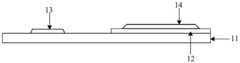
如图2-2所示,其为步骤202结束时,衬底基板的结构示意图,衬底基板11上依次形成有透明导电图案12以及多条栅线13和公共电极图案14,其中多条栅线13和公共电极图案14同层设置,且公共电极图案14与透明导电图案12电连接。As shown in FIG. 2-2, which is a schematic structural diagram of the base substrate at the end of
步骤203、在形成有多条栅线和公共电极图案的衬底基板上形成栅绝缘层。
该栅绝缘层(英文:Gate Insulator;简称:GI)可以由氮化硅等材质构成,具体可以参考相关技术,在此不再赘述。The gate insulating layer (English: Gate Insulator; GI for short) may be formed of materials such as silicon nitride. For details, reference may be made to the related art, which will not be repeated here.
步骤204、在形成有栅绝缘层的衬底基板上形成刻蚀阻挡层。
该刻蚀阻挡层(英文:Etch Stop Layer;简称:ESL)用于避免后续形成金属导电图案的过程中的刻蚀工艺发生过刻等现象时,对栅绝缘层造成损伤。The etch stop layer (English: Etch Stop Layer; abbreviation: ESL) is used to avoid damage to the gate insulating layer when over-etching and other phenomena occur in the etching process during the subsequent formation of the metal conductive pattern.
ESL也可以由氮化硅等材质构成,具体可以参考相关技术,在此不再赘述。The ESL may also be formed of materials such as silicon nitride, and the related art may be referred to for details, which will not be repeated here.
本步骤之前,还可以在栅绝缘层上形成有源层,本步骤所形成的刻蚀阻挡层上设置有过孔,该过孔由于使后续形成的金属导电图案中的源漏极能够与有源层接触。Before this step, an active layer can also be formed on the gate insulating layer, and the etching barrier layer formed in this step is provided with a via hole. source layer contact.
此外,本步骤是可选的步骤,即在本发明实施例提供的显示面板的制造方法中,也可以不在栅绝缘层上形成刻蚀阻挡层。In addition, this step is an optional step, that is, in the manufacturing method of the display panel provided by the embodiment of the present invention, an etching barrier layer may not be formed on the gate insulating layer.
步骤205、在刻蚀阻挡层和栅绝缘层上形成过孔。
该过孔用于使后续形成的金属导电层中的跨接图案能够与刻蚀阻挡层和栅绝缘层下方的公共电极层接触。在形成该过孔时,可以避免衬底基板上的TFT所在的区域,以避免过孔和后续形成的跨接图案对TFT的形成以及正常工作造成影响。The via hole is used to enable the bridge pattern in the subsequently formed metal conductive layer to be in contact with the common electrode layer under the etching barrier layer and the gate insulating layer. When the via hole is formed, the area where the TFT is located on the base substrate can be avoided, so as to avoid the influence of the via hole and the subsequently formed bridge pattern on the formation and normal operation of the TFT.
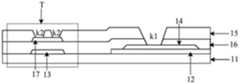
步骤205结束时,衬底基板的结构可以如图2-3所示,其中,刻蚀阻挡层15和栅绝缘层16上形成有过孔k1,刻蚀阻挡层15和栅绝缘层16下方的公共电极图案14通过该过孔k1露出。此外,位于TFT区域T中的栅绝缘层16与刻蚀阻挡层15之间可以设置有有源层17,刻蚀阻挡层15在TFT区域T中设置有过孔k2,有源层17通过该过孔k2露出。11为衬底基板。At the end of
步骤206、在形成有刻蚀阻挡层的衬底基板上形成金属导电图案。
该金属导电图案包括可以包括源漏极图案和跨接图案,而跨接图案包括多个跨接结构,多个跨接结构中的任一跨接结构通过刻蚀阻挡层和栅绝缘层上的过孔分别与位于衬底基板多条栅线中的任一栅线两侧的公共电极图案电连接。The metal conductive pattern may include a source-drain pattern and a bridging pattern, and the bridging pattern includes a plurality of bridging structures, and any bridging structure in the plurality of bridging structures is etched through the barrier layer and the gate insulating layer. The via holes are respectively electrically connected with the common electrode patterns located on both sides of any one of the plurality of gate lines in the base substrate.
步骤206结束时,衬底基板的结构可以如图2-4所示,金属导电图案18中的源漏极图案181可以形成于TFT区域T,而跨接图案182可以形成于除TFT区域T外的其他区域中。图2-4中其他标记的含义可以参考图2-3,在此不再赘述。At the end of
如图2-5所示,其为图2-4的俯视图,其中,跨接图案182中的跨接结构1821使位于栅线13两侧的公共电极图案14电连接。其中,与公共电极图案14电连接的透明导电图案12也可以作为公共电极图案14的一部分。图2-5中其他标记的含义可以参考图2-4,在此不再赘述。As shown in FIGS. 2-5 , which are the top views of FIGS. 2-4 , the
可选的,衬底基板中,每两个被栅线隔开且相邻的子像素区域中的公共电极图案通过跨接结构电连接,即每个子像素区域中的公共电极图案均通过跨接结构与预设方向(预设方向为垂直于栅线的长度方向)上相邻的两个子像素区域中的公共电极图案电连接,如此设置能够在较大程度上保证公共电极图案在各个位置的电压的一致性较强。Optionally, in the base substrate, the common electrode patterns in every two adjacent sub-pixel regions separated by gate lines are electrically connected through a bridging structure, that is, the common electrode patterns in each sub-pixel region are electrically connected through a bridging structure. The structure is electrically connected to the common electrode patterns in the two adjacent sub-pixel regions in the preset direction (the preset direction is perpendicular to the length direction of the gate line), and this arrangement can ensure that the common electrode patterns are arranged at various positions to a greater extent. The voltage consistency is strong.
相关技术中,为了提高公共电极图案各处电压的均一性(公共电极图案各处电压的均一性较差可能导致显示面板的画面泛绿),通常会对位于多条栅线中每条栅线两侧的公共电极图案进行跨接。但由于用于作为跨接结构的透明导电图案的电阻较大,因而通常不得不在每个子像素区域中设置跨接结构以提高公共电极图案的电压的一致性,但是在通过化学气相沉积(英文:Chemical Vapor Deposition;简称:CVD)技术修复数据线上可能存在的断路时,修复位置难以与跨接结构拉开一定的距离,这使得化学气相沉积技术所产生的金属粉末(如钨粉)可能会散落在跨接结构上,进而导致短路。In the related art, in order to improve the uniformity of the voltage across the common electrode pattern (poor uniformity of the voltage across the common electrode pattern may cause the image of the display panel to appear green), each gate line in the plurality of gate lines is usually The common electrode patterns on both sides are bridged. However, due to the large resistance of the transparent conductive pattern used as the jumper structure, it is usually necessary to provide a jumper structure in each sub-pixel region to improve the voltage consistency of the common electrode pattern, but in chemical vapor deposition (English: When Chemical Vapor Deposition (abbreviation: CVD) technology repairs the possible open circuit on the data line, it is difficult for the repair position to be separated from the bridge structure, which makes the metal powder (such as tungsten powder) produced by the chemical vapor deposition technology. scattered on the jumper structure, causing a short circuit.
但是,由于本发明实施例中的跨接结构有电阻较小的金属构成,因而,在衬底基板中,每个像素组所在区域中形成有一个跨接结构,每个像素组包括至少三个子像素。如此能够确保部分子像素区域中未设置有跨接结构,在通过化学气相沉积技术修复数据线时,修复位置可以与跨接结构拉开一定的距离,避免了化学气相沉积技术所产生的金属粉末散落到跨接结构上导致的短路,提高了修复的成功率。However, since the jumper structure in the embodiment of the present invention is made of metal with low resistance, in the base substrate, a jumper structure is formed in the region where each pixel group is located, and each pixel group includes at least three sub-substrates pixel. In this way, it can be ensured that some sub-pixel regions are not provided with a bridging structure. When the data line is repaired by chemical vapor deposition technology, the repair position can be separated from the bridging structure by a certain distance, avoiding the metal powder produced by chemical vapor deposition technology. Shorts caused by scattering on the jumper structure increase the success rate of repairs.
需要说明的是,本发明实施例所涉及的像素组所包括的至少三个子像素可以包括一个像素中的三个子像素,也可以包括不同像素中的三个子像素,在此不做限制。It should be noted that the at least three subpixels included in the pixel group involved in the embodiment of the present invention may include three subpixels in one pixel, or may include three subpixels in different pixels, which are not limited herein.
步骤207、在形成有多条栅线和公共电极图案的衬底基板上形成钝化层。
钝化层(英文:Passivation;简称:PVX)上可以形成有用于使源漏电极与后续形成的像素电极图案接触的过孔。The passivation layer (English: Passivation; PVX for short) may be formed with via holes for contacting the source and drain electrodes with the subsequently formed pixel electrode patterns.
步骤208、在形成有钝化层的衬底基板上形成像素电极图案。
该像素电极图案可以和步骤201形成的透明导电图案一同控制液晶层。The pixel electrode pattern can control the liquid crystal layer together with the transparent conductive pattern formed in
步骤208结束时,衬底基板的结构可以如图2-6所示,形成有金属导电图案18的衬底基板11上依次设置有钝化层19和像素电极图案191,像素电极图案191通过钝化层19上的过孔(图2-6中未标出)与金属导电图案18中的源漏极181电连接。图2-6中其他标记的含义可以参考图2-4,在此不再赘述。At the end of
本发明实施例以制造LCD为例进行说明,但本发明实施例还可以应用于制造OLED,在制造OLED时,可以不执行步骤201而直接在衬底基板上形成多条栅线和公共电极图案,此外,在步骤207所形成的并非是像素电极图案,而是OLED显示面板中有机发光器件的阳极图案,其他步骤可以参考本发明实施例,在此不再赘述。The embodiment of the present invention is described by taking the manufacture of an LCD as an example, but the embodiment of the present invention can also be applied to the manufacture of an OLED. During the manufacture of an OLED, a plurality of gate lines and common electrode patterns may be directly formed on the base substrate without performing
本发明实施例的各个包括有图案的膜层结构可以由构图工艺形成,构图工艺通常可以包括有涂覆、曝光、显影、刻蚀和剥离等步骤,具体可以参考相关技术,在此不再赘述。Each film layer structure including a pattern in the embodiments of the present invention may be formed by a patterning process, and the patterning process may generally include steps such as coating, exposure, development, etching, and stripping. For details, reference may be made to related technologies, which will not be repeated here. .
综上所述,本发明实施例提供的显示面板的制造方法,通过由金属制成的导电层中的跨接结构来使位于栅线两侧的公共电极图案电连接,减小了跨接结构的电阻,进而使得通过跨接图案进行跨接的公共电极图案各处的电压的均一性较高。解决了相关技术中由于构成透明导电图案的透明导电材料的电阻通常较大,这使得通过透明导电图案进行跨接的公共电极图案各处的电压的均一性较低的问题。达到了公共电极图案各处的电压的均一性较高的效果。To sum up, in the method for manufacturing a display panel provided by the embodiments of the present invention, the common electrode patterns located on both sides of the gate lines are electrically connected through the bridging structure in the conductive layer made of metal, thereby reducing the bridging structure. Therefore, the uniformity of the voltage across the common electrode pattern that is bridged by the jumper pattern is higher. This solves the problem in the related art that since the resistance of the transparent conductive material constituting the transparent conductive pattern is generally large, the uniformity of the voltage across the common electrode pattern bridged by the transparent conductive pattern is relatively low. It achieves the effect of higher uniformity of the voltage throughout the common electrode pattern.
本发明实施例提供的一种显示面板,该显示面板的结构可以如图2-6所示,该显示面板包括衬底基板11。An embodiment of the present invention provides a display panel. The structure of the display panel may be as shown in FIGS. 2-6 , and the display panel includes a
衬底基板11上设置有多条栅线13和公共电极图案14。A plurality of
设置有多条栅线13和公共电极图案14的衬底基板11上设置有绝缘层I。The insulating layer I is provided on the
绝缘层I上设置有过孔(图2-6中未标出)。The insulating layer I is provided with via holes (not marked in FIGS. 2-6 ).
设置有绝缘层I的衬底基板11上设置有金属导电图案18。A metal
其中,金属导电图案18包括源漏极图案181和包括多个跨接结构的跨接图案182,多个跨接结构中的任一跨接结构用于通过过孔分别与位于多条栅线13中的任一栅线两侧的公共电极图案14电连接。Wherein, the metal
可选的,绝缘层I包括栅绝缘层16和刻蚀阻挡层15,栅绝缘层16设置在设置有多条栅线13和公共电极图案14的衬底基板11上。Optionally, the insulating layer 1 includes a
刻蚀阻挡层15设置在设置有栅绝缘层16的衬底基板11上。The
可选的,衬底基板11上还设置有透明导电图案12。Optionally, the
多条栅线13和公共电极图案14设置在设置有透明导电图案12的衬底基板11上,公共电极图案14与透明导电图案12电连接。A plurality of
综上所述,本发明实施例提供的显示面板,通过由金属制成的导电层中的跨接结构来使位于栅线两侧的公共电极图案电连接,减小了跨接结构的电阻,进而使得通过跨接图案进行跨接的公共电极图案各处的电压的均一性较高。解决了相关技术中由于构成透明导电图案的透明导电材料的电阻通常较大,这使得通过透明导电图案进行跨接的公共电极图案各处的电压的均一性较低的问题。达到了公共电极图案各处的电压的均一性较高的效果。To sum up, in the display panel provided by the embodiments of the present invention, the common electrode patterns located on both sides of the gate lines are electrically connected through the bridging structure in the conductive layer made of metal, which reduces the resistance of the bridging structure, In turn, the uniformity of the voltage across the common electrode pattern bridged by the bridge pattern is high. This solves the problem in the related art that since the resistance of the transparent conductive material constituting the transparent conductive pattern is generally large, the uniformity of the voltage across the common electrode pattern bridged by the transparent conductive pattern is relatively low. It achieves the effect of higher uniformity of the voltage throughout the common electrode pattern.
此外,本发明实施例还提供一种显示装置,该显示装置可以包括图1所示方法制造的显示面板或图2-1所示方法制造的显示面板,示例的,该显示面板的结构可以如图2-6所示。In addition, an embodiment of the present invention also provides a display device. The display device may include a display panel manufactured by the method shown in FIG. 1 or a display panel manufactured by the method shown in FIG. 2-1. For example, the structure of the display panel may be as follows As shown in Figure 2-6.
需要指出的是,在附图中,为了图示的清晰可能夸大了层和区域的尺寸。而且可以理解,当元件或层被称为在另一元件或层“上”时,它可以直接在其他元件上,或者可以存在中间的层。另外,可以理解,当元件或层被称为在另一元件或层“下”时,它可以直接在其他元件下,或者可以存在一个以上的中间的层或元件。另外,还可以理解,当层或元件被称为在两层或两个元件“之间”时,它可以为两层或两个元件之间惟一的层,或还可以存在一个以上的中间层或元件。通篇相似的参考标记指示相似的元件。It should be noted that, in the drawings, the sizes of layers and regions may be exaggerated for clarity of illustration. It will also be understood that when an element or layer is referred to as being "on" another element or layer, it can be directly on the other element or intervening layers may be present. In addition, it will be understood that when an element or layer is referred to as being "under" another element or layer, it can be directly under the other element, or more than one intervening layer or element may be present. In addition, it will also be understood that when a layer or element is referred to as being 'between' two layers or elements, it can be the only layer between the two layers or elements, or more than one intervening layer may also be present or element. Like reference numerals indicate like elements throughout.
本领域普通技术人员可以理解实现上述实施例的全部或部分步骤可以通过硬件来完成,也可以通过程序来指令相关的硬件完成,所述的程序可以存储于一种计算机可读存储介质中,上述提到的存储介质可以是只读存储器,磁盘或光盘等。Those of ordinary skill in the art can understand that all or part of the steps of implementing the above embodiments can be completed by hardware, or can be completed by instructing relevant hardware through a program, and the program can be stored in a computer-readable storage medium. The storage medium mentioned may be a read-only memory, a magnetic disk or an optical disk, etc.
以上所述仅为本发明的较佳实施例,并不用以限制本发明,凡在本发明的精神和原则之内,所作的任何修改、等同替换、改进等,均应包含在本发明的保护范围之内。The above are only preferred embodiments of the present invention and are not intended to limit the present invention. Any modifications, equivalent replacements, improvements, etc. made within the spirit and principles of the present invention shall be included in the protection of the present invention. within the range.
Claims (8)
Priority Applications (2)
| Application Number | Priority Date | Filing Date | Title |
|---|---|---|---|
| CN201710876367.3ACN107680975B (en) | 2017-09-25 | 2017-09-25 | Manufacturing method of display panel, display panel and display device |
| US16/023,720US10685989B2 (en) | 2017-09-25 | 2018-06-29 | Method for manufacturing display panel, display panel, and display device |
Applications Claiming Priority (1)
| Application Number | Priority Date | Filing Date | Title |
|---|---|---|---|
| CN201710876367.3ACN107680975B (en) | 2017-09-25 | 2017-09-25 | Manufacturing method of display panel, display panel and display device |
Publications (2)
| Publication Number | Publication Date |
|---|---|
| CN107680975A CN107680975A (en) | 2018-02-09 |
| CN107680975Btrue CN107680975B (en) | 2020-11-20 |
Family
ID=61136177
Family Applications (1)
| Application Number | Title | Priority Date | Filing Date |
|---|---|---|---|
| CN201710876367.3AActiveCN107680975B (en) | 2017-09-25 | 2017-09-25 | Manufacturing method of display panel, display panel and display device |
Country Status (2)
| Country | Link |
|---|---|
| US (1) | US10685989B2 (en) |
| CN (1) | CN107680975B (en) |
Families Citing this family (2)
| Publication number | Priority date | Publication date | Assignee | Title |
|---|---|---|---|---|
| CN109713022B (en)* | 2019-01-28 | 2020-10-13 | 武汉华星光电半导体显示技术有限公司 | Display panel |
| WO2023044763A1 (en)* | 2021-09-24 | 2023-03-30 | 京东方科技集团股份有限公司 | Array substrate and display device |
Citations (3)
| Publication number | Priority date | Publication date | Assignee | Title |
|---|---|---|---|---|
| CN101373299A (en)* | 2007-08-21 | 2009-02-25 | 北京京东方光电科技有限公司 | FFS thin-film transistor LCD device pixel structure and manufacturing method thereof |
| CN103022052A (en)* | 2012-12-14 | 2013-04-03 | 京东方科技集团股份有限公司 | Array substrate and display device |
| CN104678664A (en)* | 2013-11-29 | 2015-06-03 | 乐金显示有限公司 | Liquid crystal display and method for manufacturing the same |
Family Cites Families (3)
| Publication number | Priority date | Publication date | Assignee | Title |
|---|---|---|---|---|
| CN103489826B (en)* | 2013-09-26 | 2015-08-05 | 京东方科技集团股份有限公司 | Array base palte, preparation method and display unit |
| CN105304649B (en)* | 2015-10-28 | 2019-01-18 | 京东方科技集团股份有限公司 | Array substrate and preparation method thereof, display panel, display device |
| US20170162609A1 (en)* | 2015-12-08 | 2017-06-08 | Innolux Corporation | Display panel and manufacturing method thereof |
- 2017
- 2017-09-25CNCN201710876367.3Apatent/CN107680975B/enactiveActive
- 2018
- 2018-06-29USUS16/023,720patent/US10685989B2/enactiveActive
Patent Citations (3)
| Publication number | Priority date | Publication date | Assignee | Title |
|---|---|---|---|---|
| CN101373299A (en)* | 2007-08-21 | 2009-02-25 | 北京京东方光电科技有限公司 | FFS thin-film transistor LCD device pixel structure and manufacturing method thereof |
| CN103022052A (en)* | 2012-12-14 | 2013-04-03 | 京东方科技集团股份有限公司 | Array substrate and display device |
| CN104678664A (en)* | 2013-11-29 | 2015-06-03 | 乐金显示有限公司 | Liquid crystal display and method for manufacturing the same |
Also Published As
| Publication number | Publication date |
|---|---|
| US10685989B2 (en) | 2020-06-16 |
| CN107680975A (en) | 2018-02-09 |
| US20190096924A1 (en) | 2019-03-28 |
Similar Documents
| Publication | Publication Date | Title |
|---|---|---|
| CN108288621B (en) | Manufacturing method of array substrate, array substrate and display panel | |
| CN104681567B (en) | Thin film transistor base plate and its manufacture method with metal-oxide semiconductor (MOS) | |
| US10964790B1 (en) | TFT substrate and manufacturing method thereof | |
| US8592237B2 (en) | Method of manufacturing a thin film transistor including forming bus line patterns in a substrate and filling with metal | |
| CN110047898A (en) | Display base plate and its manufacturing method, display device | |
| CN108803173A (en) | Array substrate and its manufacturing method, display device | |
| KR20100049427A (en) | Dual panel type organic electroluminescent device and method of fabricating the same | |
| CN104218095B (en) | A kind of thin film transistor (TFT) and preparation method thereof, array base palte and display unit | |
| CN108351572A (en) | Array substrate and its restorative procedure | |
| CN105607365A (en) | COA substrate and fabrication method therefor | |
| CN103187423A (en) | Oxide thin film transistor array substrate, manufacturing method of array substrate, and display panel | |
| CN108010924A (en) | A kind of array base palte and production method, display panel | |
| CN104678671B (en) | Display base plate and its manufacturing method and display device | |
| CN105810695A (en) | Array substrate and display device | |
| CN104062814B (en) | A pixel electrode layer, array substrate, display panel and display device | |
| CN104932159A (en) | Display substrate, manufacturing method of display substrate, driving method and display device | |
| CN103715135B (en) | A kind of via hole and preparation method thereof, array base palte | |
| CN104183603B (en) | Array substrate and preparation method thereof, and display device | |
| CN107680975B (en) | Manufacturing method of display panel, display panel and display device | |
| JP7295808B2 (en) | Array substrate, display panel and display device | |
| CN107422543B (en) | Display panel, preparation method thereof and display device | |
| CN105185839B (en) | TFT and its manufacturing method, driving circuit and display device | |
| CN102832170A (en) | Manufacturing method of array substrate, array substrate and display device | |
| CN106098709A (en) | Array base palte, display device | |
| CN113113428B (en) | Array substrate and preparation method thereof |
Legal Events
| Date | Code | Title | Description |
|---|---|---|---|
| PB01 | Publication | ||
| PB01 | Publication | ||
| SE01 | Entry into force of request for substantive examination | ||
| SE01 | Entry into force of request for substantive examination | ||
| GR01 | Patent grant | ||
| GR01 | Patent grant |