CN107667430B - High mobility semiconductor source/drain spacers - Google Patents
High mobility semiconductor source/drain spacersDownload PDFInfo
- Publication number
- CN107667430B CN107667430BCN201580080339.XACN201580080339ACN107667430BCN 107667430 BCN107667430 BCN 107667430BCN 201580080339 ACN201580080339 ACN 201580080339ACN 107667430 BCN107667430 BCN 107667430B
- Authority
- CN
- China
- Prior art keywords
- fin
- semiconductor material
- gate
- iii
- channel region
- Prior art date
- Legal status (The legal status is an assumption and is not a legal conclusion. Google has not performed a legal analysis and makes no representation as to the accuracy of the status listed.)
- Active
Links
Images


Classifications
- H—ELECTRICITY
- H10—SEMICONDUCTOR DEVICES; ELECTRIC SOLID-STATE DEVICES NOT OTHERWISE PROVIDED FOR
- H10D—INORGANIC ELECTRIC SEMICONDUCTOR DEVICES
- H10D64/00—Electrodes of devices having potential barriers
- H10D64/01—Manufacture or treatment
- H10D64/017—Manufacture or treatment using dummy gates in processes wherein at least parts of the final gates are self-aligned to the dummy gates, i.e. replacement gate processes
- H—ELECTRICITY
- H10—SEMICONDUCTOR DEVICES; ELECTRIC SOLID-STATE DEVICES NOT OTHERWISE PROVIDED FOR
- H10D—INORGANIC ELECTRIC SEMICONDUCTOR DEVICES
- H10D30/00—Field-effect transistors [FET]
- H10D30/01—Manufacture or treatment
- H10D30/021—Manufacture or treatment of FETs having insulated gates [IGFET]
- H10D30/024—Manufacture or treatment of FETs having insulated gates [IGFET] of fin field-effect transistors [FinFET]
- H—ELECTRICITY
- H10—SEMICONDUCTOR DEVICES; ELECTRIC SOLID-STATE DEVICES NOT OTHERWISE PROVIDED FOR
- H10D—INORGANIC ELECTRIC SEMICONDUCTOR DEVICES
- H10D30/00—Field-effect transistors [FET]
- H10D30/60—Insulated-gate field-effect transistors [IGFET]
- H10D30/62—Fin field-effect transistors [FinFET]
- H10D30/6211—Fin field-effect transistors [FinFET] having fin-shaped semiconductor bodies integral with the bulk semiconductor substrates
- H—ELECTRICITY
- H10—SEMICONDUCTOR DEVICES; ELECTRIC SOLID-STATE DEVICES NOT OTHERWISE PROVIDED FOR
- H10D—INORGANIC ELECTRIC SEMICONDUCTOR DEVICES
- H10D30/00—Field-effect transistors [FET]
- H10D30/60—Insulated-gate field-effect transistors [IGFET]
- H10D30/67—Thin-film transistors [TFT]
- H10D30/6729—Thin-film transistors [TFT] characterised by the electrodes
- H10D30/673—Thin-film transistors [TFT] characterised by the electrodes characterised by the shapes, relative sizes or dispositions of the gate electrodes
- H10D30/6735—Thin-film transistors [TFT] characterised by the electrodes characterised by the shapes, relative sizes or dispositions of the gate electrodes having gates fully surrounding the channels, e.g. gate-all-around
- H—ELECTRICITY
- H10—SEMICONDUCTOR DEVICES; ELECTRIC SOLID-STATE DEVICES NOT OTHERWISE PROVIDED FOR
- H10D—INORGANIC ELECTRIC SEMICONDUCTOR DEVICES
- H10D30/00—Field-effect transistors [FET]
- H10D30/60—Insulated-gate field-effect transistors [IGFET]
- H10D30/67—Thin-film transistors [TFT]
- H10D30/6757—Thin-film transistors [TFT] characterised by the structure of the channel, e.g. transverse or longitudinal shape or doping profile
- H—ELECTRICITY
- H10—SEMICONDUCTOR DEVICES; ELECTRIC SOLID-STATE DEVICES NOT OTHERWISE PROVIDED FOR
- H10D—INORGANIC ELECTRIC SEMICONDUCTOR DEVICES
- H10D30/00—Field-effect transistors [FET]
- H10D30/60—Insulated-gate field-effect transistors [IGFET]
- H10D30/751—Insulated-gate field-effect transistors [IGFET] having composition variations in the channel regions
- H—ELECTRICITY
- H10—SEMICONDUCTOR DEVICES; ELECTRIC SOLID-STATE DEVICES NOT OTHERWISE PROVIDED FOR
- H10D—INORGANIC ELECTRIC SEMICONDUCTOR DEVICES
- H10D62/00—Semiconductor bodies, or regions thereof, of devices having potential barriers
- H10D62/10—Shapes, relative sizes or dispositions of the regions of the semiconductor bodies; Shapes of the semiconductor bodies
- H10D62/13—Semiconductor regions connected to electrodes carrying current to be rectified, amplified or switched, e.g. source or drain regions
- H10D62/149—Source or drain regions of field-effect devices
- H10D62/151—Source or drain regions of field-effect devices of IGFETs
- H—ELECTRICITY
- H10—SEMICONDUCTOR DEVICES; ELECTRIC SOLID-STATE DEVICES NOT OTHERWISE PROVIDED FOR
- H10D—INORGANIC ELECTRIC SEMICONDUCTOR DEVICES
- H10D62/00—Semiconductor bodies, or regions thereof, of devices having potential barriers
- H10D62/10—Shapes, relative sizes or dispositions of the regions of the semiconductor bodies; Shapes of the semiconductor bodies
- H10D62/17—Semiconductor regions connected to electrodes not carrying current to be rectified, amplified or switched, e.g. channel regions
- H10D62/213—Channel regions of field-effect devices
- H10D62/221—Channel regions of field-effect devices of FETs
- H10D62/235—Channel regions of field-effect devices of FETs of IGFETs
- H10D62/292—Non-planar channels of IGFETs
- H—ELECTRICITY
- H10—SEMICONDUCTOR DEVICES; ELECTRIC SOLID-STATE DEVICES NOT OTHERWISE PROVIDED FOR
- H10D—INORGANIC ELECTRIC SEMICONDUCTOR DEVICES
- H10D62/00—Semiconductor bodies, or regions thereof, of devices having potential barriers
- H10D62/80—Semiconductor bodies, or regions thereof, of devices having potential barriers characterised by the materials
- H10D62/82—Heterojunctions
- H10D62/824—Heterojunctions comprising only Group III-V materials heterojunctions, e.g. GaN/AlGaN heterojunctions
- H—ELECTRICITY
- H10—SEMICONDUCTOR DEVICES; ELECTRIC SOLID-STATE DEVICES NOT OTHERWISE PROVIDED FOR
- H10D—INORGANIC ELECTRIC SEMICONDUCTOR DEVICES
- H10D64/00—Electrodes of devices having potential barriers
- H10D64/01—Manufacture or treatment
- H10D64/021—Manufacture or treatment using multiple gate spacer layers, e.g. bilayered sidewall spacers
- H—ELECTRICITY
- H10—SEMICONDUCTOR DEVICES; ELECTRIC SOLID-STATE DEVICES NOT OTHERWISE PROVIDED FOR
- H10D—INORGANIC ELECTRIC SEMICONDUCTOR DEVICES
- H10D64/00—Electrodes of devices having potential barriers
- H10D64/20—Electrodes characterised by their shapes, relative sizes or dispositions
- H10D64/27—Electrodes not carrying the current to be rectified, amplified, oscillated or switched, e.g. gates
- H10D64/311—Gate electrodes for field-effect devices
- H10D64/411—Gate electrodes for field-effect devices for FETs
- H10D64/511—Gate electrodes for field-effect devices for FETs for IGFETs
- H10D64/517—Gate electrodes for field-effect devices for FETs for IGFETs characterised by the conducting layers
- H10D64/518—Gate electrodes for field-effect devices for FETs for IGFETs characterised by the conducting layers characterised by their lengths or sectional shapes
- H—ELECTRICITY
- H10—SEMICONDUCTOR DEVICES; ELECTRIC SOLID-STATE DEVICES NOT OTHERWISE PROVIDED FOR
- H10D—INORGANIC ELECTRIC SEMICONDUCTOR DEVICES
- H10D84/00—Integrated devices formed in or on semiconductor substrates that comprise only semiconducting layers, e.g. on Si wafers or on GaAs-on-Si wafers
- H10D84/01—Manufacture or treatment
- H10D84/0123—Integrating together multiple components covered by H10D12/00 or H10D30/00, e.g. integrating multiple IGBTs
- H10D84/0126—Integrating together multiple components covered by H10D12/00 or H10D30/00, e.g. integrating multiple IGBTs the components including insulated gates, e.g. IGFETs
- H10D84/0165—Integrating together multiple components covered by H10D12/00 or H10D30/00, e.g. integrating multiple IGBTs the components including insulated gates, e.g. IGFETs the components including complementary IGFETs, e.g. CMOS devices
- H10D84/0167—Manufacturing their channels
- H—ELECTRICITY
- H10—SEMICONDUCTOR DEVICES; ELECTRIC SOLID-STATE DEVICES NOT OTHERWISE PROVIDED FOR
- H10D—INORGANIC ELECTRIC SEMICONDUCTOR DEVICES
- H10D84/00—Integrated devices formed in or on semiconductor substrates that comprise only semiconducting layers, e.g. on Si wafers or on GaAs-on-Si wafers
- H10D84/01—Manufacture or treatment
- H10D84/0123—Integrating together multiple components covered by H10D12/00 or H10D30/00, e.g. integrating multiple IGBTs
- H10D84/0126—Integrating together multiple components covered by H10D12/00 or H10D30/00, e.g. integrating multiple IGBTs the components including insulated gates, e.g. IGFETs
- H10D84/0165—Integrating together multiple components covered by H10D12/00 or H10D30/00, e.g. integrating multiple IGBTs the components including insulated gates, e.g. IGFETs the components including complementary IGFETs, e.g. CMOS devices
- H10D84/017—Manufacturing their source or drain regions, e.g. silicided source or drain regions
- H—ELECTRICITY
- H10—SEMICONDUCTOR DEVICES; ELECTRIC SOLID-STATE DEVICES NOT OTHERWISE PROVIDED FOR
- H10D—INORGANIC ELECTRIC SEMICONDUCTOR DEVICES
- H10D84/00—Integrated devices formed in or on semiconductor substrates that comprise only semiconducting layers, e.g. on Si wafers or on GaAs-on-Si wafers
- H10D84/01—Manufacture or treatment
- H10D84/0123—Integrating together multiple components covered by H10D12/00 or H10D30/00, e.g. integrating multiple IGBTs
- H10D84/0126—Integrating together multiple components covered by H10D12/00 or H10D30/00, e.g. integrating multiple IGBTs the components including insulated gates, e.g. IGFETs
- H10D84/0165—Integrating together multiple components covered by H10D12/00 or H10D30/00, e.g. integrating multiple IGBTs the components including insulated gates, e.g. IGFETs the components including complementary IGFETs, e.g. CMOS devices
- H10D84/0172—Manufacturing their gate conductors
- H10D84/0179—Manufacturing their gate conductors the gate conductors having different shapes or dimensions
- H—ELECTRICITY
- H10—SEMICONDUCTOR DEVICES; ELECTRIC SOLID-STATE DEVICES NOT OTHERWISE PROVIDED FOR
- H10D—INORGANIC ELECTRIC SEMICONDUCTOR DEVICES
- H10D84/00—Integrated devices formed in or on semiconductor substrates that comprise only semiconducting layers, e.g. on Si wafers or on GaAs-on-Si wafers
- H10D84/01—Manufacture or treatment
- H10D84/0123—Integrating together multiple components covered by H10D12/00 or H10D30/00, e.g. integrating multiple IGBTs
- H10D84/0126—Integrating together multiple components covered by H10D12/00 or H10D30/00, e.g. integrating multiple IGBTs the components including insulated gates, e.g. IGFETs
- H10D84/0165—Integrating together multiple components covered by H10D12/00 or H10D30/00, e.g. integrating multiple IGBTs the components including insulated gates, e.g. IGFETs the components including complementary IGFETs, e.g. CMOS devices
- H10D84/0193—Integrating together multiple components covered by H10D12/00 or H10D30/00, e.g. integrating multiple IGBTs the components including insulated gates, e.g. IGFETs the components including complementary IGFETs, e.g. CMOS devices the components including FinFETs
- H—ELECTRICITY
- H10—SEMICONDUCTOR DEVICES; ELECTRIC SOLID-STATE DEVICES NOT OTHERWISE PROVIDED FOR
- H10D—INORGANIC ELECTRIC SEMICONDUCTOR DEVICES
- H10D84/00—Integrated devices formed in or on semiconductor substrates that comprise only semiconducting layers, e.g. on Si wafers or on GaAs-on-Si wafers
- H10D84/01—Manufacture or treatment
- H10D84/02—Manufacture or treatment characterised by using material-based technologies
- H10D84/03—Manufacture or treatment characterised by using material-based technologies using Group IV technology, e.g. silicon technology or silicon-carbide [SiC] technology
- H10D84/038—Manufacture or treatment characterised by using material-based technologies using Group IV technology, e.g. silicon technology or silicon-carbide [SiC] technology using silicon technology, e.g. SiGe
- H—ELECTRICITY
- H10—SEMICONDUCTOR DEVICES; ELECTRIC SOLID-STATE DEVICES NOT OTHERWISE PROVIDED FOR
- H10D—INORGANIC ELECTRIC SEMICONDUCTOR DEVICES
- H10D84/00—Integrated devices formed in or on semiconductor substrates that comprise only semiconducting layers, e.g. on Si wafers or on GaAs-on-Si wafers
- H10D84/01—Manufacture or treatment
- H10D84/02—Manufacture or treatment characterised by using material-based technologies
- H10D84/08—Manufacture or treatment characterised by using material-based technologies using combinations of technologies, e.g. using both Si and SiC technologies or using both Si and Group III-V technologies
- H—ELECTRICITY
- H10—SEMICONDUCTOR DEVICES; ELECTRIC SOLID-STATE DEVICES NOT OTHERWISE PROVIDED FOR
- H10D—INORGANIC ELECTRIC SEMICONDUCTOR DEVICES
- H10D84/00—Integrated devices formed in or on semiconductor substrates that comprise only semiconducting layers, e.g. on Si wafers or on GaAs-on-Si wafers
- H10D84/80—Integrated devices formed in or on semiconductor substrates that comprise only semiconducting layers, e.g. on Si wafers or on GaAs-on-Si wafers characterised by the integration of at least one component covered by groups H10D12/00 or H10D30/00, e.g. integration of IGFETs
- H10D84/82—Integrated devices formed in or on semiconductor substrates that comprise only semiconducting layers, e.g. on Si wafers or on GaAs-on-Si wafers characterised by the integration of at least one component covered by groups H10D12/00 or H10D30/00, e.g. integration of IGFETs of only field-effect components
- H10D84/83—Integrated devices formed in or on semiconductor substrates that comprise only semiconducting layers, e.g. on Si wafers or on GaAs-on-Si wafers characterised by the integration of at least one component covered by groups H10D12/00 or H10D30/00, e.g. integration of IGFETs of only field-effect components of only insulated-gate FETs [IGFET]
- H10D84/85—Complementary IGFETs, e.g. CMOS
- H10D84/853—Complementary IGFETs, e.g. CMOS comprising FinFETs
Landscapes
- Insulated Gate Type Field-Effect Transistor (AREA)
- Thin Film Transistor (AREA)
- Junction Field-Effect Transistors (AREA)
Abstract
Translated fromChinese
Description
Translated fromChinese背景技术Background technique
对扩展集成电路系统(IC)的摩尔定律的努力已经包含了采用除硅之外的材料(例如III-V化合物半导体材料(例如InP、InGaAs、InAs))的晶体管的发展。这些非硅材料系统通常显示比硅设备更高的载流子迁移率,并且因此它们的引入已经被长期建议作为朝向更快晶体管的路径。然而,与更高载流子迁移率一起,在场效应晶体管(FET)中,与对于相等有效(电)沟道长度的硅基FET相比,对于III-V(和Ge)沟道式设备,在源极与漏极之间的断开状态(Ioff)泄露能够是显著更高的。因为断开状态泄露通常是有效沟道长度的指数函数,所以可能不清楚的是,如何可以通过使用高迁移率半导体材料来改进晶体管密度,而不是晶体管速度。Efforts to extend Moore's Law for integrated circuit systems (ICs) have included the development of transistors employing materials other than silicon, such as III-V compound semiconductor materials (eg, InP, InGaAs, InAs). These non-silicon material systems generally exhibit higher carrier mobilities than silicon devices, and thus their introduction has long been suggested as a route towards faster transistors. However, along with higher carrier mobility, in field effect transistors (FETs), for III-V (and Ge) channel-type devices, compared to silicon-based FETs of equivalent effective (electrical) channel length, Off-state (Ioff ) leakage between source and drain can be significantly higher. Because off-state leakage is generally an exponential function of effective channel length, it may not be clear how transistor density, but not transistor speed, can be improved by using high-mobility semiconductor materials.
附图说明Description of drawings
作为示例而非作为限制来在附图中图示本文描述的材料。为了说明的简洁和清晰,在附图中图示的元件不一定按比例绘制。例如,为了清晰,一些元件的尺寸相对于其它元件可能被放大。此外,在认为适当的情况下,已经在附图之中重复参考标签以指示对应或类似元件。在附图中:The materials described herein are illustrated in the accompanying drawings by way of example and not by way of limitation. For simplicity and clarity of illustration, elements illustrated in the figures have not necessarily been drawn to scale. For example, the dimensions of some elements may be exaggerated relative to other elements for clarity. Further, where considered appropriate, reference labels have been repeated among the figures to indicate corresponding or analogous elements. In the attached image:
图1是根据一些实施例的包含设置在衬底之上的硅沟道式鳍式FET和高迁移率鳍式FET的互补金属氧化物半导体(CMOS)电路系统的俯视图;1 is a top view of a complementary metal-oxide-semiconductor (CMOS) circuit system including silicon channel finFETs and high mobility finFETs disposed over a substrate in accordance with some embodiments;
图2A图示根据一些实施例的通过在图1中描绘的高迁移率鳍式FET的源极/漏极和沟道区域的长度的横截面视图;2A illustrates a cross-sectional view through the length of the source/drain and channel regions of the high mobility finFET depicted in FIG. 1 in accordance with some embodiments;
图2B图示根据一些实施例的通过在图1中描绘的高迁移率鳍式FET的源极/漏极区域内鳍宽度的横截面视图;2B illustrates a cross-sectional view through the fin width within the source/drain regions of the high mobility finFET depicted in FIG. 1 in accordance with some embodiments;
图2C图示根据一些实施例的通过在图1中描绘的高迁移率鳍式FET的横向沟道区域内鳍宽度的横截面视图;2C illustrates a cross-sectional view of the width of the fin through the lateral channel region of the high mobility finFET depicted in FIG. 1 in accordance with some embodiments;
图3A图示根据一些备选的实施例的通过在图1中描绘的高迁移率鳍式FET的源极/漏极和沟道区域的长度的横截面视图;3A illustrates a cross-sectional view through the length of the source/drain and channel regions of the high mobility finFET depicted in FIG. 1, according to some alternative embodiments;
图3B图示根据一些备选的实施例的通过在图1中描绘的高迁移率鳍式FET的源极/漏极区域内鳍宽度的横截面视图;3B illustrates a cross-sectional view through the fin width within the source/drain regions of the high mobility finFET depicted in FIG. 1 in accordance with some alternative embodiments;
图3C图示根据一些备选的实施例的通过在图1中描绘的高迁移率鳍式FET的横向沟道区域内鳍宽度的横截面视图;3C illustrates a cross-sectional view of the width of the fin through the lateral channel region of the high mobility finFET depicted in FIG. 1 in accordance with some alternative embodiments;
图4A图示根据一些备选的实施例的通过在图1中描绘的高迁移率鳍式FET的源极/漏极和沟道区域的长度的横截面视图;4A illustrates a cross-sectional view through the length of the source/drain and channel regions of the high mobility finFET depicted in FIG. 1, according to some alternative embodiments;
图4B图示根据一些备选的实施例的通过在图1中描绘的高迁移率鳍式FET的源极/漏极区域内鳍宽度的横截面视图;4B illustrates a cross-sectional view through the fin width within the source/drain regions of the high mobility finFET depicted in FIG. 1 in accordance with some alternative embodiments;
图4C图示根据一些备选的实施例的通过在图1中描绘的高迁移率鳍式FET的横向沟道区域内鳍宽度的横截面视图;4C illustrates a cross-sectional view of fin widths within a lateral channel region through the high mobility finFET depicted in FIG. 1 in accordance with some alternative embodiments;
图5图示根据一些备选的实施例的通过在图1中描绘的高迁移率鳍式FET的源极/漏极和沟道区域的长度的横截面视图;5 illustrates a cross-sectional view through the length of the source/drain and channel regions of the high mobility finFET depicted in FIG. 1, according to some alternative embodiments;
图6是图示根据一些实施例的制作具有高迁移率半导体源极/漏极隔离物的高迁移率鳍式FET的方法的流程图;6 is a flowchart illustrating a method of fabricating a high mobility finFET with high mobility semiconductor source/drain spacers in accordance with some embodiments;
图7A、7B、7C、7D、7E和7F图示根据一些实施例的随着执行在图6中图示的方法演进的通过高迁移率鳍式FET的源极/漏极区域和沟道区域的长度的横截面视图;Figures 7A, 7B, 7C, 7D, 7E, and 7F illustrate source/drain regions and channel regions through a high mobility finFET as the method illustrated in Figure 6 is performed, according to some embodiments A cross-sectional view of the length of ;
图8A、8B、8C、8D、8E和8F图示根据一些实施例的随着执行在图4中图示的方法演进的通过高迁移率鳍式FET的区域内的鳍结构的宽度的横截面视图;Figures 8A, 8B, 8C, 8D, 8E, and 8F illustrate cross-sections of widths of fin structures in regions through high mobility fin FETs that evolve as the method illustrated in Figure 4 is performed, according to some embodiments view;
图9图示根据本发明实施例的采用包含多个高迁移率鳍式FET的SoC的数据服务器机器和移动计算平台,所述多个高迁移率鳍式FET包含高迁移率半导体源极/漏极隔离物;以及9 illustrates a data server machine and mobile computing platform employing a SoC comprising a plurality of high mobility finFETs comprising high mobility semiconductor source/drain, according to an embodiment of the present invention pole spacers; and
图10是根据本发明实施例的电子计算设备的功能框图。10 is a functional block diagram of an electronic computing device according to an embodiment of the present invention.
具体实施方式Detailed ways
参考所附的图来描述一个或多个实施例。虽然详细论述和描绘了特定配置和布置,但应该理解的是,这只是出于说明性目的而进行的。相关领域的技术人员将认识到,其它配置和布置是可能的,而不背离本描述的精神和范围。对于相关领域的技术人员,可在除了本文详细描述的系统和应用以外的各种其它系统和应用中采用本文描述的技术和/或布置将是显而易见的。One or more embodiments are described with reference to the accompanying figures. While specific configurations and arrangements have been discussed and depicted in detail, it should be understood that this is done for illustrative purposes only. Those skilled in the relevant art will recognize that other configurations and arrangements are possible without departing from the spirit and scope of the present description. It will be apparent to those skilled in the relevant art that the techniques and/or arrangements described herein may be employed in various other systems and applications in addition to those described in detail herein.
在下面的详细描述中参考附图,附图形成其一部分并且图示示范实施例。此外,要理解的是,可以利用其它实施例,并且可进行结构和/或逻辑改变而不背离要求的主题的范围。还应该注意的是,例如上、下、顶部、底部等的方向和参考可将仅仅用来促进附图中的特征的描述。因此,下面的详细的描述不在限制意义上进行,并且要求的主题的范围仅由所附的权利要求以及它们的等同物来限定。In the following detailed description, reference is made to the accompanying drawings, which form a part hereof and illustrate exemplary embodiments. Furthermore, it is to be understood that other embodiments may be utilized and structural and/or logical changes may be made without departing from the scope of the claimed subject matter. It should also be noted that directions and references such as upper, lower, top, bottom, etc., may only be used to facilitate description of features in the figures. Therefore, the following detailed description is not to be taken in a limiting sense, and the scope of the claimed subject matter is defined only by the appended claims and their equivalents.
在下面的描述中,阐述了众多细节。然而,对于本领域的技术人员,在没有这些特定细节的情况下可以实践本发明将是显而易见的。在一些实例中,以框图形式而不是详细地示出众所周知的方法和设备,以避免使本发明模糊。在本说明书通篇中对“实施例”、“一个实施例”或“一些实施例”的提及意味着,结合实施例描述的具体特征、结构、功能或特性包含在本发明的至少一个实施例中。因此,在本说明书通篇各处出现的短语“在实施例中”或“在一个实施例中”或“在一些实施例中”不一定表示本发明的相同的实施例。此外,在一个或多个实施例中,可以以任何适合的方式组合具体特征、结构、功能或特性。例如,在与两个实施例关联的具体特征、结构、功能或特性不相互排斥的任何地方,第一实施例可与第二实施例组合。In the following description, numerous details are set forth. However, it will be apparent to one skilled in the art that the present invention may be practiced without these specific details. In some instances, well-known methods and devices are shown in block diagram form, rather than in detail, in order to avoid obscuring the present invention. Reference throughout this specification to "an embodiment," "one embodiment," or "some embodiments" means that a particular feature, structure, function, or characteristic described in connection with the embodiments is included in at least one implementation of the invention example. Thus, appearances of the phrases "in an embodiment" or "in one embodiment" or "in some embodiments" in various places throughout this specification are not necessarily referring to the same embodiment of the invention. Furthermore, the particular features, structures, functions, or characteristics may be combined in any suitable manner in one or more embodiments. For example, the first embodiment may be combined with the second embodiment wherever the specific features, structures, functions or characteristics associated with the two embodiments are not mutually exclusive.
如在描述和所附的权利要求中使用的,单数形式“一”、“一个”和“所述”也意图包含复数形式,除非上下文另有明确指示。还将理解的是,如本文所使用的术语“和/或”表示并且囊括所关联的列出项目中的一个或多个的任何以及所有可能组合。As used in the description and the appended claims, the singular forms "a," "an," and "the" are intended to include the plural forms as well, unless the context clearly dictates otherwise. It will also be understood that the term "and/or" as used herein means and includes any and all possible combinations of one or more of the associated listed items.
术语“耦合”和“连接”连同它们的派生词在本文中可用来描述组件之间的功能或结构关系。应该理解的是,这些术语不意图作为彼此的同义词。相反,在具体实施例中,“连接”可用来指示两个或更多元件彼此直接物理、光或电接触。“耦合”可用来指示两个或更多元件彼此直接或者间接(其中其它中间元件在它们之间)物理或电接触,和/或两个或更多元件彼此合作或相互作用(例如,如处于因果关系中)。The terms "coupled" and "connected", along with their derivatives, may be used herein to describe a functional or structural relationship between components. It should be understood that these terms are not intended as synonyms for each other. Rather, in particular embodiments, "connected" may be used to indicate that two or more elements are in direct physical, optical, or electrical contact with each other. "Coupled" may be used to indicate that two or more elements are in direct or indirect physical or electrical contact with each other (with other intervening elements between them), and/or two or more elements cooperate or interact with each other (eg, as in causality).
如本文所使用的术语“在...之上”、“在...之下”、“在...之间”以及“在...上”表示一个组件或材料相对于其它组件或材料的相对位置,其中此类物理关系是值得注意的。例如,在材料的上下文中,设置在另一材料之上或之下的一个材料或材料可直接在接触中,或者可具有一个或多个中间材料。此外,设置在两个材料或材料之间的一个材料可与两个层直接接触,或者可具有一个或多个中间层。相比之下,在第二材料或材料“上”的第一材料或材料与那个第二材料/材料直接接触。在组件组装的上下文中将做出类似的区别。The terms "on", "under", "between" and "on" as used herein mean one component or material relative to another component or The relative position of materials in which such physical relationships are of note. For example, in the context of materials, one material or materials disposed above or below another material may be directly in contact, or may have one or more intervening materials. Furthermore, a material disposed between two materials or materials may be in direct contact with both layers, or may have one or more intervening layers. In contrast, a first material or material "on" a second material or material is in direct contact with that second material/material. Similar distinctions will be made in the context of component assembly.
如在本描述通篇以及权利要求书中所使用的,通过术语“…中的至少一个”或“…中的一个或多个”结合的项目的列表能够意味着所列术语的任何组合。例如,短语“A、B或C中的至少一个”能够意味着A;B;C;A和B;A和C;B和C;或者A、B和C。As used throughout this description and in the claims, a list of items joined by the terms "at least one of" or "one or more of" can mean any combination of the listed terms. For example, the phrase "at least one of A, B, or C" can mean A; B; C; A and B; A and C; B and C;
进一步根据扩展摩尔定律时,用来定标(scale)FET栅极长度并维持沟道的良好栅极控制的一种方式是要这样做,而不影响源极/漏极距离,这取决于设备体系结构可必需将轻掺杂(或不掺杂)的源极/漏极尖端区域从栅极叠层(gate stack)之下更远地移出。一个示例是从“重叠的栅极”移动到“欠重叠的栅极”,这通常增大了对于给定栅极长度Lg的有效沟道长度Leff。硅基晶体管中的较大欠重叠的缺点是使性能降级的显著增大的晶体管电阻。而且,如果例如通过减小栅极长度同时增大欠重叠来减小晶体管单元的占用空间或面积,则源极/漏极面积可能也需要减少,潜在地加剧了由较大欠重叠引起的晶体管电阻中的增大。Further on extending Moore's Law, one way to scale the FET gate length and maintain good gate control of the channel is to do so without affecting the source/drain distance, depending on the device Architectures may necessitate moving the lightly doped (or undoped) source/drain tip regions further out of the gate stack. One example is moving from "overlapped gate" to "under-overlapped gate", which generally increases the effective channel lengthLeff for a given gate length Lg. The disadvantage of larger under-overlap in silicon-based transistors is a significantly increased transistor resistance that degrades performance. Also, if the footprint or area of a transistor cell is reduced, for example, by reducing gate length while increasing under-overlap, source/drain area may also need to be reduced, potentially exacerbating transistors caused by larger under-overlap increase in resistance.
在下面进一步描述的实施例中,对于多数载流子晶体管沟道采用高迁移率半导体材料。如本文所使用的,“高迁移率”材料是除了硅之外的半导体材料,所述半导体材料具有比用于硅的对应沟道的那个载流子的迁移率更高的载流子迁移率。值得注意的是,在载流子迁移率更高的情况下,与对于参考硅FET的源极/漏极(尖端)区域的栅极欠重叠相比,源极/漏极(尖端)区域的栅极欠重叠可被更显著地增大,因为关联的电阻惩罚不那么严重。增大欠重叠的这个更大的自由度可被利用(leverage),以维持足以保持在阈值晶体管泄露水平以下的有效沟道长度。在另外的实施例中,无需增大晶体管单元的面积,或者通过减小源极/漏极面积,通过在不平行(例如正交)于横向栅极长度的方向上延伸沟道长度,增大欠重叠的这个更大自由度被利用。在一些有利的实施例中,增大欠重叠的这个更大自由度被利用以减小晶体管单元的面积,而不使晶体管性能特性降级到参考硅沟道式设备的晶体管性能特性以下,实现更大的设备密度。In embodiments described further below, a high mobility semiconductor material is used for the majority carrier transistor channel. As used herein, a "high mobility" material is a semiconductor material other than silicon that has a higher carrier mobility than that for the corresponding channel of silicon . It is worth noting that at higher carrier mobility, the source/drain (tip) region of the source/drain (tip) region has less gate overlap compared to the gate under-overlap for the source/drain (tip) region of the reference silicon FET. Gate under-overlap can be increased more significantly because the associated resistance penalty is less severe. This greater degree of freedom to increase under-overlap can be leveraged to maintain effective channel lengths sufficient to remain below threshold transistor leakage levels. In further embodiments, without increasing the area of the transistor cell, or by reducing the source/drain area, increasing the channel length in a direction that is not parallel (eg, orthogonal) to the lateral gate length This greater degree of freedom of under-overlap is exploited. In some advantageous embodiments, this greater freedom of increasing under-overlap is exploited to reduce the area of the transistor cell without degrading the transistor performance characteristics below that of the reference silicon channel device, enabling more Large device density.
在下面进一步描述的一些实施例中,单片FET包含设置在衬底之上的第一高迁移率半导体材料中的多数载流子沟道。栅极叠层被设置在第一半导体材料的横向沟道区域之上。一对源极/漏极区域与横向沟道区域至少垂直间隔开高迁移率半导体材料的厚度。在一些实施例中,在横向沟道区域中采用的相同高迁移率半导体材料提供垂直间隔。与横向沟道区域相比,第一高迁移率半导体材料则具有基本上更大的膜厚度,如垂直于基础界面和/或衬底所测量的。穿过源极与漏极之间最短Leff的载流子可因此不仅在栅极叠层之下横向穿过,而且通过半导体源极/漏极隔离物穿过附加距离。因为这个附加距离能够基本上正交于与图案化的栅极关联的横向沟道长度,所以设备密度可被改进。In some embodiments described further below, a monolithic FET includes a majority carrier channel in a first high mobility semiconductor material disposed over a substrate. A gate stack is disposed over the lateral channel region of the first semiconductor material. A pair of source/drain regions and the lateral channel region are vertically spaced apart by at least a thickness of the high mobility semiconductor material. In some embodiments, the same high mobility semiconductor material employed in the lateral channel region provides vertical spacing. The first high mobility semiconductor material then has a substantially greater film thickness, as measured perpendicular to the base interface and/or the substrate, than the lateral channel region. Carriers traversing the shortestLeff between source and drain can thus not only traverse laterally under the gate stack, but also traverse an additional distance through the semiconductor source/drain spacers. Because this additional distance can be substantially orthogonal to the lateral channel length associated with the patterned gate, device density can be improved.
在下面进一步描述的一些实施例中,虽然掩膜(例如栅极叠层或牺牲的栅极叠层)正覆盖横向沟道区域,但具有高载流子迁移率并且有利地低杂质掺杂的半导体材料被过度生长,例如环绕电介质隔离物并且增大晶体管源极与漏极之间的Leff,而没有晶体管占用空间中的伴随增大。代替晶体管单元面积增大,掺杂的源极/漏极膜和/或源极/漏极接触金属化件的厚度相反被对应地减小。将晶体管沟道区域定义为其将重掺杂的源极半导体与重掺杂的漏极半导体分开的区域,高迁移率半导体隔离物也可被描述为延伸超出栅极叠层的正交沟道区域。下面还在一个或多个非平面(鳍式)FET晶体管体系结构的上下文中进一步描述相对于使横向沟道区域凹陷而过度生长半导体隔离物以形成正交沟道区域的优点。In some embodiments described further below, although a mask (eg, a gate stack or a sacrificial gate stack) is covering the lateral channel region, it has high carrier mobility and advantageously low impurity doping. The semiconductor material is overgrown, eg, surrounding the dielectric spacer and increasing theLeff between the transistor source and drain without a concomitant increase in the transistor footprint. Instead of increasing the transistor cell area, the thicknesses of the doped source/drain films and/or source/drain contact metallizations are instead correspondingly reduced. Defining the transistor channel region as the region that separates the heavily doped source semiconductor from the heavily doped drain semiconductor, the high mobility semiconductor spacer can also be described as an orthogonal channel extending beyond the gate stack area. The advantages of overgrowing semiconductor spacers to form orthogonal channel regions relative to recessing lateral channel regions are further described below in the context of one or more non-planar (fin) FET transistor architectures.
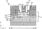
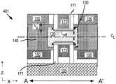
图1是根据一些实施例的包含设置在衬底105之上并且由隔离材料180包围的硅沟道式鳍式FET 102和高迁移率鳍式FET 101的互补金属氧化物半导体(CMOS)电路系统100的俯视图。在示范实施例中,鳍式FET 101是NMOS设备,而鳍式FET 102是PMOS设备。对于此类实施例,鳍式FET 102可具有任何体系结构,而鳍式FET 101具有下面进一步描述的特征中的一个或多个特征。在备选的实施例中,高迁移率NMOS鳍式FET 101与高迁移率PMOS鳍式FET 102耦合。对于此类备选的实施例,鳍式FET 101和鳍式FET 102两者可具有下面进一步描述的特征中的一个或多个特征。1 is a complementary metal oxide semiconductor (CMOS) circuit system including a
在一些实施例中,衬底105是硅(Si),其对于鳍式FET 101和102的单片集成是有利的。在示范实施例中基本上单晶的衬底105的晶体取向是(100)、(111)或(110)。然而,其它晶体取向也是可能的。例如,衬底工作表面可以朝向[110] 2°-10°被斜切(miscut)或偏切(offcut),以促进晶体异质外延材料的成核。其它衬底实施例也是可能的。例如,衬底105可以是碳化硅(SiC)、蓝宝石、III-V化合物半导体(例如GaAs)、绝缘体上硅(SOI)、锗(Ge)或锗化硅(SiGe)中的任何。隔离材料180可以是适合于提供晶体管之间的电隔离的任何材料。在一些示范实施例中,隔离材料180是二氧化硅。还可利用已知适合于该目的其它材料,包含低k材料(例如具有在2.5以下的相对电介质常数)。In some embodiments,
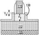
在图示的实施例中,鳍式FET 101与比与鳍式FET 102关联的晶体管单元面积小的晶体管单元面积关联。具体来说,与鳍式FET 101关联的栅极长度Lg小于与鳍式FET 102关联的对应栅极长度Lg,2。为了清楚,源极/漏极接触金属化件150与栅极电极173的边缘之间的源极/漏极接触长度Lc和横向间隔Ls对于两个鳍式FET 101、102都是相等的。因此,在这个示例中,鳍式FET 101中的栅极长度收缩表示鳍式FET 101相对于鳍式FET 102的源极/漏极接触金属化件节距Pc中的减小。最长横向长度鳍103则可比鳍104的对应长度短。在其中鳍式FET 101的接入电阻相对高的其它实施例中,鳍式FET 101中的栅极长度收缩可被用于增大的源极/漏极接触长度Lc,而不将鳍式FET 101的接触金属化件节距Pc增大超出鳍式FET102的接触金属化件节距。如上所述,与对于可比较的有效沟道长度的硅沟道式设备的断开状态泄漏电流相比,对于高迁移率沟道材料的断开状态泄漏电流通常是显著更高的。因此,在一些实施例中,鳍式FET 101的有效沟道长度与栅极长度Lg之间的差大于鳍式FET 102的有效沟道长度与栅极长度Lg,2之间的对应差。如下面进一步描述的,设置在横向间隔131内的高迁移率半导体源极/漏极隔离物计及这个较大差。In the illustrated embodiment,
尽管特定尺寸随着设备技术形成而变化,但在其中Lg,2是近似10nm的一个示例中,Lg可以小2-5nm,提供高达50%的横向栅极收缩。在横向间隔131(其例如可以是3-5nm)内,高迁移率半导体源极/漏极隔离物可隔开(stand-off)重掺杂的源极/漏极区域附加的1-5nm。在有效沟道长度中的总体增大则是2-10nm。因此,即使在较短栅极长度(即Lg<Lg,2)的情况下,与鳍式FET 102的有效沟道长度相比,鳍式FET 101可具有更长的有效沟道长度。取决于断开状态泄露如何根据对于具体高迁移率沟道材料的有效沟道长度而变化,鳍式FET 102因此可显示与鳍式FET 102的断开状态泄露相比更好或可比较的断开状态泄露。值得注意的是,没有高迁移率材料的使用,与较大有效沟道长度关联的电阻中的增大通常将导致晶体管性能中的净降级。横向尺寸收缩因此对于硅基设备将是不太有利的,实际上减小fmax以实现具有给定ft的更大密度的设备。然而,如果沟道属于使fmax能够保持与较慢硅沟道式设备同等的适合的高(空穴)迁移率材料(例如Ge),则可应用类似的方法以收缩PMOS鳍式FET102的单元,无需此种牺牲。Although specific dimensions vary with device technology formation, in one example where Lg,2 is approximately 10 nm,Lg can be 2-5 nm smaller, providing up to 50% lateral gate shrinkage. Within the lateral spacing 131 (which may be, for example, 3-5 nm), the high mobility semiconductor source/drain spacers may stand-off the heavily doped source/drain regions for an additional 1-5 nm. The overall increase in effective channel length is then 2-10 nm. Therefore, even with a shorter gate length (ie, Lg < Lg,2 ), the
在实施例中,非平面半导体主体(即鳍)的横向宽度从栅极长度Lg内的最小值变化到栅极叠层的边缘之外的主体的端部内的最大值。例如,如图1所图示的,鳍式FET 101具有在栅极金属173之下的并且由虚线标示的最小横向鳍宽度Wf,1。鳍宽度Wf,1可随实现变化,但在示范实施例中,小于20nm,并且有利地小于10nm。至少在横向间隔131内的鳍宽度是大于Wf,1的Wf,2。Wf,1与Wf,2之间的差指示高迁移率半导体源极/漏极隔离物。在一些有利实施例中,Wf,1与Wf,2之间的差是高迁移率半导体源极/漏极隔离物的厚度的近似两倍(例如2-10nm)。在另外的实施例中,鳍式FET 101的最小鳍宽度等于鳍式FET 102的鳍宽度(即,也是Wf,1)。如图1中进一步注意的,至少对于示范硅沟道实施例鳍式FET 102,间隔131内的横向鳍宽度在Wf,1保持不变。In an embodiment, the lateral width of the non-planar semiconductor body (ie, the fin) varies from a minimum value within the gate lengthLg to a maximum value within the ends of the body beyond the edge of the gate stack. For example, as illustrated in FIG. 1 ,
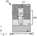
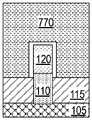
第一高迁移率材料的鳍可直接设置在衬底上,或某种中间材料上。在一些示范实施例中,晶体管101包含半导体异质结鳍(“异质鳍”)结构103,其进一步包含设置在第二高迁移率材料的“副鳍”上的第一高迁移率材料,如下面进一步描述的。图2A图示根据一些实施例的通过沿在图1中标示的A-A'平面的高迁移率鳍式FET 101的源极/漏极和沟道区域长度的横截面视图。异质鳍103包含设置在第二半导体材料的副鳍110上的高迁移率半导体材料的鳍120。不同成分的两种材料形成异质结135。在其中副鳍110不将充当设备沟道的一部分的示范实施例中,副鳍110不需要属于具有高电子迁移率的材料。在一些有利实施例中,副鳍110是适合成分的第二材料,使得异质结135与导致至少对于减少通过副鳍110的泄漏电流有用的鳍120与副鳍110之间的传导带偏移的带隙差异(bandgap differential)关联。The fins of the first high mobility material may be disposed directly on the substrate, or on some intermediate material. In some demonstrative embodiments,
在一些实施例中,副鳍110和鳍120各自是具有来自周期表的III族的至少一个元素(例如Al、Ga、In等)的第一子晶格和周期表的V族的至少一个元素(例如N、P、As、Sb等)的第二子晶格的单晶体。副鳍110和鳍120各自可以是分别包含来自周期表的III和V族的两个、三个乃至四个元素的二元、三元或四元III-V化合物半导体。In some embodiments, sub-fin 110 and
因为鳍120是N型晶体管101的设备层,所以它有利地是具有高电子迁移率的III-V材料,例如但不限于InGaAs、InP、InSb和InAs。对于一些示范InGaAs鳍实施例,In的摩尔分数在0.2与0.8之间。在一些有利的实施例中,在栅极叠层(包含栅极电介质172和栅极电极173)正下方设置的鳍120的横向沟道区域是本征III-V材料,并且不为了最高迁移率而故意采用任何电活性杂质掺杂。在备选的实施例中,标称背景n型掺杂剂水平可存在于横向沟道区域内,例如以便设置阈值电压Vt。Because
副鳍110有利地是具有对鳍材料的显著(例如传导)带偏移的III-V材料,例如但不限于GaAs、GaSb、GaAsSb、GaP、InAlAs、GaAsSb、AlAs、AlP、AlSb和AlGaAs。在一些实施例中,鳍120和副鳍110属于互补杂质类型。例如,在鳍120将提供电子多数载流子沟道的情况下,副鳍110可采用p型杂质(例如Mg、Be等)掺杂。
鳍120包含设置在栅极电极173和栅极电介质172之下(或被其覆盖)的横向沟道区域。横向沟道区域进一步被设置在邻近栅极电极173相对边的电介质横向隔离物171之下(或被其覆盖)。在一些实施例中,高迁移率半导体隔离物包括与横向沟道区域相同的半导体材料。对于此类实施例,在横向沟道区域与半导体隔离物之间可能不存在组合界面。在备选实施例中,高迁移率半导体隔离物包括与横向沟道区域不同的半导体材料。
图2A图示其中高迁移率半导体隔离物包括与横向沟道区域相同的半导体材料的示范实施例。虚线框因此标示半导体隔离物130。对于其中高迁移率半导体隔离物包括与横向沟道区域不同的半导体材料的实施例,虚线框内的材料成分将不同于下面的栅极电极173。如所示出的,半导体隔离物130从横向沟道区域和栅极电介质172的界面垂直(例如在z维度中)延伸。换言之,半导体隔离物130具有比横向沟道区域大高迁移率半导体隔离物厚度Vs的膜厚度(如在从基础界面垂直的方向上所测量的)。因而,有效沟道长度Leff,1包含横向距离(例如沿x轴延伸)和不平行于(例如正交于)横向距离的垂直距离(例如沿z轴延伸)两者。如下面进一步注意的,对于在至少两个维度中的对称沟道长度延伸,正交沟道区域垂直(例如在z维度中)和横向(例如在y维度中)都延伸。2A illustrates an exemplary embodiment in which the high mobility semiconductor spacer includes the same semiconductor material as the lateral channel region. The dashed box thus marks the
在通过图2A进一步图示的一些实施例中,半导体隔离物130横向(例如在x维度中)延伸超出横向隔离物171的外部边缘基本上(即+/-10%)与半导体隔离物130垂直延伸超出横向隔离物171的外部边缘相同的量。换言之,半导体隔离物130在z维度和x维度中都延伸超出横向隔离物171 Vs。对于此类实施例,最小有效沟道长度至少等于Leff,1。例如,甚至由Leff,2表示的排他的横向载流子路径至少等于Leff,1。排他的横向载流子路径例如可在鳍120的纵向轴处被发现,而其它路径将包含正交分量。因此根据半导体隔离物130在三个维度(例如从与鳍120相交的横向隔离物171的边缘上的点)中对称延伸,有效沟道长度在鳍120的整个电流携带体积之上是基本上相等的。In some embodiments, further illustrated by FIG. 2A , the outer edges of the
在一些实施例中,半导体隔离物130具有与横向沟道区域相同的材料成分。晶格(子晶格)成分和杂质浓度两者有利地是相同的,使得半导体隔离物130在功能上是鳍120的连续同质的部分。在一些实施例中,在横向沟道区域是本征(即没有故意掺杂)的情况下,半导体隔离物130也是本征的。例如,在横向沟道区域是本征InGaAs的情况下,半导体隔离物130也可以是本征InGaAs。在一些备选的实施例中,半导体隔离物130具有与鳍120的横向沟道部分相同的多数晶格组分,但具有不同的杂质掺杂。例如,可将半导体隔离物130 n型轻掺杂到比鳍120的横向沟道部分的杂质浓度更高的杂质浓度。例如,在横向沟道区域是本征InGaAs的情况下,半导体隔离物130可以是n型轻掺杂的InGaAs。在一些备选的实施例中,半导体隔离物130具有与鳍120的横向沟道部分不同的多数晶格组分,但具有相同的杂质掺杂。例如,在横向沟道区域是本征InGaAs(其中In的第一摩尔分数在0.2与0.8之间)的情况下,半导体隔离物130可以是本征InGaAs,其中In的第二(不同)摩尔分数在0.2与0.8之间。In some embodiments, the
在由图2A表示的一些实施例中,半导体隔离物130环绕横向隔离物171。横向隔离物171可以是任何电介质材料,并且可与栅极电极173的侧壁接触,或者如所示出的,与覆盖栅极电极173的侧壁的栅极电介质172接触。横向隔离物171的横向尺寸例如可在从0(其中半导体隔离物130与栅极电极173仅由栅极电介质172分开)和10nm的任何地方变化。在一些示范实施例中,横向隔离物171在栅极电极173与半导体隔离物130之间提供了3-5nm的横向间隔。偏压的栅极电极到半导体隔离物130的静电耦合能够是显著的、变得更多,以便横向隔离物171的尺寸朝向0减小。对于此类实施例,Vs可接近栅极电极173的z高度以获得预期的有效沟道长度。In some embodiments represented by FIG. 2A ,
如通过图2A进一步图示的,再生长的异质外延源极/漏极区域140与半导体隔离物130对接。在一些实施例中,源极/漏极区域140包括具有与鳍120的晶格组分截然不同的晶格组分的III-V化合物半导体,以给接触金属化件150提供促进低电阻的有利的低带隙。第二异质结136因此存在于源极/漏极区域140与半导体隔离物130之间。异质外延源极/漏极区域140可属于适合于到鳍120的欧姆接触的任何材料,例如但不限于InAs。在一些实施例中,源极/漏极材料140是单晶的。源极/漏极区域140有利地被重掺杂(例如在InAs实施例中为n型)。如图2A中所示出的,源极/漏极区域140覆盖半导体隔离物130,使得金属化件150与源极/漏极区域140对接,而不是与半导体隔离物130对接,即便接触金属化件有点未对准。取决于源极/漏极区域140的z高度,半导体隔离物130可被或多或少的源极/漏极材料覆盖,所述源极/漏极材料能够被期望输送紧靠近栅极叠层的相当大的电流。As further illustrated by FIG. 2A , regrown heteroepitaxial source/
在由图2A表示的一些实施例中,源极/漏极区域140仅形成一个异质结136。没有采用副鳍110形成第二异质结,因为鳍120在副鳍110的整个长度之上延伸。如下面进一步描述的,设置在源极/漏极区域140与副鳍110之间的鳍120的区域指示被采用以形成半导体隔离物130的技术。在一些示范实施例中,设置在源极/漏极区域140与副鳍110之间的鳍120的区域的厚度基本上(即,+/-10%)等于高迁移率半导体隔离物厚度Vs。如下面进一步描述的,与半导体隔离物厚度Vs的这个关系指示被采用以形成半导体隔离物130的再生长技术。除了指示被采用以形成半导体隔离物130的技术之外,在源极/漏极区域140与副鳍110之间的鳍120的存在可提供减少源极/漏极区域140与副鳍110之间的泄露的有利的带隙偏移。在源极/漏极区域140与副鳍110之间的鳍120的存在还可提供重掺杂的源极/漏极区域140与副鳍110之间的有利阻碍(setback),减少n型掺杂剂到副鳍110中的扩散,这另外可能增大源极/漏极区域140与副鳍110之间的泄漏电流。In some embodiments represented by FIG. 2A , the source/
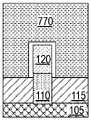
图2B图示根据一些实施例的通过沿在图1中标示的B-B'平面的异质鳍宽度的横截面视图。B-B'平面通过高迁移率半导体隔离物130内的鳍式FET 101的源极/漏极区域140,接近高迁移率半导体隔离物130,异质结136(图2A)形成与鳍120的跨横向鳍宽度Wf,2的界面。如图2B中进一步图示的,半导体隔离物厚度Vs作为标示沿整个鳍z高度Hf的鳍120的延伸的虚线是可见的。相比之下,半导体隔离物厚度Vs基本上不在嵌入在副鳍隔离115内的副鳍110的多数中。副鳍隔离115可以是适合于提供邻近副鳍之间的电隔离的任何非晶材料。在一些示范实施例中,副鳍隔离115是二氧化硅。也可采用其它已知电介质材料,包含低k材料。尽管实施例在这方面上不受限,但是其它示范材料包含碳掺杂的氧化物、硅氧烷衍生物等等。2B illustrates a cross-sectional view through a heterogeneous fin width along the BB' plane designated in FIG. 1, in accordance with some embodiments. The BB' plane passes through the source/
如在图2B中进一步注意的,半导体隔离物130的角部分具有比至少等于Vs的鳍宽度Wf,1大的角厚度221。在示范实施例中,角厚度221显著(例如至少20%)大于Vs。值得注意的是,角厚度221指示被采用以形成半导体隔离物130的技术。如下面进一步描述的,对于其中半导体隔离物130是鳍120的过度生长(即,在定义鳍宽度Wf,1的鳍120表面上外延生长)的示范实施例,加速的外延角生长将确保在鳍120的角处的有效沟道长度不显著短于任何别的地方,并且实际上,将有可能是更长的(例如角厚度221大于Vs),降低了在这些位置处的电流密度,否则这些地方可能经受电流拥挤效应。As further noted in FIG. 2B , the corner portions of the
图2C图示根据一些实施例的通过沿在图1中描绘的C-C'平面的高迁移率鳍式FET101的横向沟道区域内鳍宽度的横截面视图。如所图示的,金属绝缘体栅极叠层包含栅极电介质材料172和栅极电极材料173。虽然可利用任何已知的栅极叠层材料,但在一个示范实施例中,将具有9或更大的体相对电介质常数的高k材料与具有适合于鳍120成分的功函的栅极金属一起用作栅极电介质。在通过图2C图示的示范实施例中,栅极电介质172被直接设置在定义横向鳍宽度Wf,1的鳍120的侧壁上。正如上面对于图2B所注意的,通过图2C图示的横向沟道区域内的鳍120的“角”指示被采用以形成半导体隔离物130(图2B)的技术。例如,如果已经执行了栅极凹槽蚀刻以将宽度Wf,2的鳍减小到横向沟道区域内的Wf,1,则在图2中图示的鳍120的轮廓将显示比在图2B的轮廓中表示的多得多的角侵蚀(corner erosion)。正如外延生长在角处加速一样,在特征的外侧角处的较大固体角度也加速了凹槽蚀刻机制。2C illustrates a cross-sectional view of the width of the fin through the lateral channel region of the
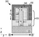
值得注意的是,上面在鳍式FET 101的上下文中描述的体系结构元件可应用于各种各样的其它鳍式FET体系结构。图3A-3C例如描绘了根据一些备选的实施例的鳍式FET201。鳍式FET 201具有与在图1中所图示的鳍式FET 101的布局基本上相同的布局。然而,鳍式FET 201采用设置在全高度鳍120之上的凸起的源极/漏极区域140。作为另外的示例,图4A-4C描绘了具有与在图1中图示的鳍式FET 101的布局基本上相同的布局的鳍式FET 301。然而,鳍式FET 301具有环绕副鳍的侧壁的高迁移率沟道。作为又一示例,图5描绘了具有与在图1中图示的鳍式FET 101的布局基本上相同的布局的纳米线FET 401。然而,纳米线FET401具有完全环绕高迁移率沟道材料的栅极叠层和源极/漏极区域。Notably, the architectural elements described above in the context of
图3A图示根据一些备选的实施例的通过在图1中描绘的A-A'平面的鳍式FET 201的横截面视图。图3B图示根据一些备选的实施例的通过在图1中描绘的B-B'平面的鳍式FET201的横截面视图。同样,图3C图示根据一些备选的实施例的通过在图1中描绘的C-C平面的鳍式FET 201的横截面视图。首先参考图3A,副鳍110和鳍120可具有上面在鳍式FET 101的上下文中论述的性质中的任何性质。与半导体隔离物130(图3B)关联的材料厚度Vs隔开凸起的源极/漏极区域140。源极/漏极区域140可再次具有上面在鳍式FET 101的上下文中描述的性质中的任何性质(例如异质外延高掺杂的窄带隙材料)。如通过图3B进一步图示的,源极/漏极区域140在鳍120的端部周围形成壳。在图3B中图示的轮廓可应用在整个源极/漏极接触长度之上,因为超出横向隔离物171的鳍120的z高度是不变的(即,源极/漏极区域140不替代鳍120的任何部分)。最小的有效栅极长度Leff因此增大(两倍)Vs。对于其中在图3C中图示的横向沟道部分的外部表皮内携带大部分源极/漏极电流的实施例,最小的有效栅极长度Leff将是占优势的,其中更接近鳍120纵向轴的载流子路径具有更长的有效沟道长度。3A illustrates a cross-sectional view of
图4A图示根据一些备选的实施例的通过在图1中描绘的A-A'平面的鳍式FET 301的横截面视图。图4B图示根据一些备选的实施例的通过在图1中描绘的B-B'平面的鳍式FET301的横截面视图。同样,图4C图示根据一些备选的实施例的通过在图1中描绘的C-C平面的鳍式FET 301的横截面视图。首先参考图4A,副鳍110和鳍120可具有上面在鳍式FET 101的上下文中论述的性质中的任何性质。与半导体隔离物130关联的膜厚度Vs(图4B)再次隔开凸起的源极/漏极区域140。源极/漏极区域140可具有上面在鳍式FET 101的上下文中描述的性质中的任何性质(例如异质外延高掺杂的窄带隙材料)。在鳍式FET 301中,鳍120在副鳍110周围包覆或形成壳,其几乎延伸全部鳍高度Hf。在此体系结构中,异质鳍103包括两种材料110、120的半径向堆叠。取决于尺寸,鳍式FET 101可操作为单门控表面沟道设备或双门控沟道设备。如图4B和4C所示出的,异质鳍103的横向沟道部分与源极/漏极端之间的差由包覆的厚度中的变化引起(例如,包覆的厚度在源极/漏极端处增大Vs)。4A illustrates a cross-sectional view of
图5图示根据一些实施例的通过在图1中描绘的A-A'平面的纳米线FET 401的横截面视图。如所示出的,半导体隔离物130基本上对称于鳍120的纵向轴CL。在这个说明性实施例中,没有已经完全采用栅极叠层材料、源极/漏极140和接触金属化件150替代的副鳍。采用具有比横向沟道区域的径向尺寸大的径向尺寸的半导体隔离物130,纳米线FET 401的沟道沿横向栅极长度Lg有效地颈缩(neck),使源极/漏极电流径向以及纵向流过鳍120。5 illustrates a cross-sectional view of a
可通过应用各种技术和处理室配置的各种方法来制作根据以上体系结构的高迁移率鳍式FET。图6是图示根据一些实施例的用于制作具有高迁移率半导体隔离物的高迁移率鳍式FET的示范方法601的流程图。图7A、7B、7C、7D、7E和7F图示根据一些实施例的随着执行方法601演进的沿鳍式FET 101的A-A'平面的横截面视图。图8A、8B、8C、8D、8E和8F图示根据一些实施例的随着执行在图6中图示的方法演进的沿鳍式FET 101的B-B'平面的横截面视图。High mobility finFETs according to the above architectures can be fabricated by applying various techniques and various methods of processing chamber configurations. 6 is a flowchart illustrating an
首先参考图6,方法601在操作610处开始,其中形成高迁移率材料的鳍。在一些实施例中,例如通过在具有多个引晶表面区域的硅衬底之上外延生长III-V材料的多个岛,制作III-V异质结鳍。在一些此类实施例中,引晶表面区域由高纵横比侧壁包围,以实践纵横比设陷(ART),并在异质外延鳍材料中实现可接受的晶体质量。ART技术是局部附加异质外延鳍制作的一个示例,其可有利地减少跨各种异质结的热失配的效应。在备选实施例中,可采用常规减去技术,其中衬垫(blanket)III-V膜叠层在衬底的整个工作表面之上生长,或者转移到衬底的整个工作表面,或者转移到衬底。服从于方法601的随后操作,那个衬垫膜叠层然后被类似地蚀刻成鳍结构。Referring first to FIG. 6,
在通过图7A和8A图示的示范实施例中,在完成操作610时,异质鳍103被设置在衬底105上,其中鳍120的至少一部分延伸超出周围副鳍隔离115 z高度Hf。在一些实施例中,z高度Hf通过从异质鳍103周围凹槽蚀刻预定量的副鳍隔离材料115来定义。z高度Hf可随着凹槽蚀刻的程度变化,潜在地暴露副鳍110的侧壁。在备选的实施例中,可利用阻挡层来确保副鳍隔离115的顶部表面与副鳍110与鳍120之间的异质结齐平。在这点上,横向鳍宽度Wf,1沿鳍120的整个纵向长度是基本上不变的。In the exemplary embodiment illustrated by Figures 7A and 8A, upon completion of
返回到图6,方法601在操作620处继续,其中将沟道掩膜被图案化,以保护将变成FET沟道区域的高迁移率鳍的部分。虽然在操作620处可采用任何已知加掩膜技术和一个或多个材料,但在一些实施例中,沟道掩膜是通过多个过程保留直到在“后栅极”鳍式FET制作流程中被替代的栅极芯棒。此类实施例可有利地与硅沟道式鳍式FET制作兼容,例如使PMOS晶体管能够同时在衬底的其它区域(未描绘)中制作。Returning to FIG. 6,
在图7B和8B中图示的示范实施例中,在异质鳍103的一部分之上形成牺牲栅极770。在操作620处可采用任何已知的牺牲栅极结构和制作技术,以在鳍120的至少两个相对侧壁上形成牺牲栅极770。将牺牲栅极770图案化成在鳍120的沟道区域之上延伸并且在副鳍隔离115上着落的牺牲材料的条纹。暴露异质鳍103的其它部分。在由图7B表示的另外实施例中,沟道掩膜进一步包含邻近牺牲栅极770的电介质横向侧壁隔离物171。在操作620处可采用任何常规自对准横向隔离物过程以从牺牲栅极770横向隔开随后的处理。例如,电介质(例如二氧化硅和/或氮化硅)可共形地沉积在异质鳍之上和在沟道掩膜之上。然后采用各向异性蚀刻来清理除了沿外形边缘(edged of topography)之外的电介质。In the exemplary embodiment illustrated in FIGS. 7B and 8B , a
返回到图6,方法601在操作630处继续,其中高迁移率材料在由沟道掩膜或副鳍隔离未保护的鳍的表面上外延生长。这个高迁移率材料可具有与鳍相同或不同的成分。因而,可利用过度生长过程的特性和暴露的鳍部分的特征来采用高迁移率半导体材料恰当地隔开随后形成的源极/漏极区域。在一些实施例中,高迁移率隔离物材料基本上作为源极/漏极区域的过度生长而生长,除了隔离物的外延生长的材料基本上采用低得多的原处(in-situ)掺杂进行生长。在一些实施例中,过度生长的材料具有与鳍的晶体引晶表面的成分相同的成分,包含相同的(低)杂质掺杂剂浓度,或者具有可能比引晶鳍材料略高的杂质浓度。Returning to FIG. 6,
取决于设备沟道的体系结构(例如体鳍、包覆等)和源极/漏极的体系结构(例如替代、凸起等),可在高迁移率隔离物的外延过度生长之前凹槽蚀刻未被沟道掩膜或副鳍隔离保护的鳍的部分。在通过图7B图示的示例中,凹槽蚀刻未被沟道掩膜或副鳍隔离115保护的鳍120的部分。此凹槽蚀刻可以或者可以不将横向隔离物171底切某一预定量。例如可采用晶体湿蚀刻剂,或者低损害的化学干蚀刻剂。在一些实施例中,鳍120被有选择地凹槽蚀刻成副鳍110。一旦鳍120和/或副鳍110的表面已经准备好引晶外延生长,就再生长鳍120的高迁移率材料。Depending on the device channel architecture (e.g. body fins, cladding, etc.) and source/drain architecture (e.g. substitution, bumps, etc.), groove etch may precede epitaxial overgrowth of high mobility spacers Portion of the fin not protected by trench mask or sub-fin isolation. In the example illustrated by FIG. 7B , the grooves etch the portions of
如在图7C中进一步图示的,例如通过金属有机化学气相沉积(MOCVD)、分子束外延(MBE)、混合气相外延(HVPE)等等中的任何,生长高迁移率半导体隔离物130。外延材料(例如InGaAs或其它III-V材料)可以是本征的(即,不是故意原处掺杂的)。如在图7C中图示的,过度生长环绕横向隔离物171,将有效的鳍高度Hf增大了量Vs,并将鳍宽度Wf,1增大到Wf,2。As further illustrated in Figure 7C, high
在备选的实施例中,在操作630处不执行鳍120的凹槽蚀刻,并且相反,仅在鳍120的侧壁上过度生长高迁移率半导体隔离物130,以将有效鳍高度Hf增大了厚度Vs,并将鳍宽度Wf,1增大到Wf,2。In an alternative embodiment, groove etching of the
在完成高迁移率材料的过度生长时,方法601继续操作640,其中形成源极/漏极区域。在操作640的一些实施例中,继续在操作630处发起的鳍120的外延再生长和/或过度生长。然而,代替基本上不掺杂,生长重掺杂的半导体。在另外的实施例中,与鳍120的成分不同的成分的重掺杂的III-V半导体从半导体隔离物130的引晶表面异质外延生长。可采用任何已知的外延源极/漏极再生长技术。在图7D和8D中进一步图示的示范实施例中,然后通过任何已知技术生长单晶体异质外延源极/漏极区域140。这个材料(例如InAs或其它III-V材料)可被原处重掺杂(例如n型)。Upon completion of the overgrowth of the high mobility material,
返回到图6,方法601在操作650处继续,其中采用永久栅极叠层替代沟道掩膜。方法601然后基本上采用在操作660处执行的任何适合的接触金属化和后端处理来完成。对于在图7E和7E中进一步图示的示范实施例,沉积并且平面化鳍式FET隔离180以暴露牺牲栅极770的顶部。相对于隔离180有选择地移除牺牲栅极770,由此暴露鳍120的横向沟道区域。在这点上,可执行可选的栅极沟道凹槽蚀刻以进一步增大正交沟道分量。对于此种栅极凹陷,鳍120的至少两个侧壁被回蚀(例如1-3nm)。值得注意的是,此种凹槽蚀刻可能不如外延再生长操作630一样可控,并且因此可以避免,如果再生长操作实现预期的源极/漏极隔离物距离(即Vs)的话。Returning to FIG. 6,
在可选的沟道(栅极)凹槽蚀刻之后,如在图7F和8F中描绘的,在鳍结构的至少两个侧壁之上形成包含栅极电介质172和栅极电极173的永久栅极叠层。虽然可利用任何已知栅极叠层材料,但在一个示范实施例中,高k电介质材料与具有适合于鳍120的III-V成分的功函的金属栅极电极一起沉积。如在图7F和8F中进一步图示的,源极/漏极接触金属化件150通过任何已知技术形成。鳍式FET 101然后基本上如图1和2A-2C中所介绍的。After optional channel (gate) recess etching, as depicted in Figures 7F and 8F, a permanent gate comprising
图9图示采用包含例如如在本文别处所描述的具有高迁移率半导体隔离物的III-V鳍式FET的SoC的数据服务器机器和移动计算平台。服务器机器906可以是例如包含设置在机架内并且连网在一起以用于电子数据处理的任何数量的高性能计算平台的任何商业服务器,所述服务器机器906在示范实施例中包含封装的单片SoC 950。移动计算平台905可以是配置用于电子数据显示、电子数据处理、无线电子数据传送等中的每个的任何便携式设备。例如,移动计算平台905可以是平板电脑、智能电话、膝上型计算机等中的任何,并且可包含显示屏(例如电容性、电感性、电阻性或光学触摸屏)、芯片级或封装级集成系统910和电池915。9 illustrates a data server machine and mobile computing platform employing an SoC including, for example, III-V FinFETs with high mobility semiconductor spacers as described elsewhere herein.
不管是设置在展开视图920中图示的集成系统910内,还是作为服务器机器906内的独立封装的芯片,封装的单片SoC 950包含存储器块(例如RAM)、处理器块(例如微处理器、多核微处理器、图形处理器等等),其包含例如如在本文别处所描述的具有高迁移率半导体隔离物的至少一个异质外延III-V n型晶体管。单片SoC 950可连同功率管理集成电路(PMIC)930、包含宽带RF(无线)传送器和/或接收器(TX/RX)(例如包含数字基带,并且模拟前端模块进一步包括传送路径上的功率放大器和接收路径上的低噪声放大器)的RF(无线)集成电路(RFIC)925以及控制器935中的一个或多个一起进一步耦合到板、衬底或内插器960。Whether disposed within the
在功能上,PMIC 930可执行电池功率调节、DC到DC转换等,并且因此具有耦合到电池915的输入以及带有向其它功能模块提供电流供应的输出。如进一步图示的,在示范实施例中,RFIC 925具有耦合到天线(未示出)以实现多个无线标准或协议中的任何的输出,所述无线标准或协议包含但不限于Wi-Fi(IEEE 802.11系列)、WiMAX(IEEE 802.16系列)、IEEE 802.20、长期演进(LTE)、Ev-DO、HSPA+、HSDPA+、HSUPA+、EDGE、GSM、GPRS、CDMA、TDMA、DECT、蓝牙及其衍生物,以及被指定为3G、4G、4G以及以上的任何其它无线协议。在备选实现中,这些板级模块中的每个都可被集成到单独IC上,或集成到单片SoC 950中。Functionally, the
图10是根据本发明的实施例的电子计算设备的功能框图。例如在平台905或服务器机器906内部可发现计算设备1000。设备1000进一步包含托管多个组件(例如但不限于处理器1004(例如应用处理器))的母板1002,其可进一步结合例如如在本文别处所描述的具有高迁移率半导体隔离物的至少一个III-V 鳍式FET。处理器1004可物理和/或电耦合到母板1002。在一些示例中,处理器804包含封装在处理器10904内的集成电路管芯。通常,术语“处理器”或“微处理器”可表示处理来自寄存器和/或存储器的电子数据以将那个电子数据变换成可进一步存储在寄存器和/或存储器中的其它电子数据的任何设备或设备的一部分。10 is a functional block diagram of an electronic computing device according to an embodiment of the present invention.
在各种示例中,一个或多个通信芯片1006也可物理和/或电耦合到母板1002。在另外的实现中,通信芯片1006可以是处理器1004的部分。取决于它的应用,计算设备1000可包含可以或者可以不物理和电耦合到母板1002的其它组件。这些其它组件包含但不限于易失性存储器(例如DRAM)、非易失性存储器(例如ROM)、闪速存储器、图形处理器、数字信号处理器、密码处理器、芯片集、天线、触摸屏显示器、触摸屏控制器、电池、音频编解码器、视频编解码器、功率放大器、全球定位系统(GPS)设备、罗盘、加速计、陀螺仪、扬声器、照相机和大容量存储设备(例如硬盘驱动、固态驱动(SSD)、光盘(CD)、数字通用盘(DVD)等)等等。In various examples, one or
通信芯片1006可实现无线通信,以用于来往于计算设备1000传递数据。术语“无线”及它的派生词可用来描述可通过使用通过非固态媒介的调制的电磁辐射传递数据的电路、设备、系统、方法、技术、通信信道等。该术语并不暗示所关联的设备不含有任何导线,尽管在一些实施例中它们可能不含有。通信芯片1006可实现多个无线标准或协议中的任何,所述无线标准或协议包含但不限于本文别处描述的那些标准或协议。如所论述的,计算设备1000可包含多个通信芯片1006。例如,第一通信芯片可专用于较短程无线通信(例如Wi-Fi和蓝牙),而第二通信芯片可专用于较长程无线通信(例如GPS、EDGE、GPRS、CDMA、WiMAX、LTE、Ev-DO及其它)。
虽然已经参考各种实现描述了本文阐述的某些特征,但本描述不意图在限制的意义上解释。因此,对本公开属于的领域中的技术人员显然的是,本文描述的实现的各种修改以及其它实现被认为处于本公开的精神和范围内。While certain features set forth herein have been described with reference to various implementations, this description is not intended to be interpreted in a limiting sense. Accordingly, various modifications of the implementations described herein, as well as other implementations, that are apparent to those skilled in the art to which this disclosure pertains are deemed to be within the spirit and scope of this disclosure.
将认识到,本发明不限于如此描述的实施例,但能够采用修改和变更实践,而不背离所附的权利要求的范围。例如,以上实施例可包含如下面进一步提供的特征的特定组合。It will be appreciated that the present invention is not limited to the embodiments so described, but can be practiced with modification and alteration without departing from the scope of the appended claims. For example, the above embodiments may include specific combinations of features as provided further below.
在一个或多个第一实施例中,单片晶体管包括设置在衬底之上的第一半导体材料。在鳍的横向沟道区域之上设置栅极叠层。一对半导体源极/漏极区域与栅极叠层通过栅极侧壁隔离物横向间隔开,并且与横向沟道区域垂直间隔开具有比源极/漏极区域低的杂质浓度的半导体材料的厚度。In one or more first embodiments, a monolithic transistor includes a first semiconductor material disposed over a substrate. A gate stack is provided over the lateral channel region of the fin. A pair of semiconductor source/drain regions are laterally spaced from the gate stack by gate sidewall spacers and vertically spaced from the lateral channel regions of a semiconductor material having a lower impurity concentration than the source/drain regions thickness.
在第一实施例的至少一个中,源极/漏极区域与横向沟道区域垂直间隔开第一半导体材料的厚度,并且第一半导体具有比硅的载流子迁移率大的载流子迁移率。In at least one of the first embodiments, the source/drain regions are vertically spaced from the lateral channel regions by a thickness of the first semiconductor material, and the first semiconductor has a greater carrier mobility than that of silicon Rate.
在紧接上面的实施例中,鳍在栅极侧壁隔离物之外距衬底的第一高度大于鳍在横向沟道区域内的第二高度,并且鳍在栅极侧壁隔离物之外的第一宽度大于鳍在横向沟道区域内的第二宽度。In the immediately above embodiment, the first height of the fin from the substrate outside the gate sidewall spacer is greater than the second height of the fin within the lateral channel region, and the fin is outside the gate sidewall spacer The first width of the is greater than the second width of the fin within the lateral channel region.
在紧接上面的实施例中,鳍的第一宽度比鳍的第二宽度大第一高度与第二高度之间差的两倍。In the immediately above embodiment, the first width of the fin is greater than the second width of the fin by twice the difference between the first and second heights.
在第一实施例的至少一个中,第一半导体材料包括设置在第二III-V化合物半导体的副鳍上的第一III-V化合物半导体材料的鳍。一对源极/漏极区域进一步包括与第一III-V化合物半导体材料接触的第三III-V化合物半导体材料。第三III-V化合物半导体与第二III-V化合物半导体材料通过第一III-V化合物半导体材料分开。In at least one of the first embodiments, the first semiconductor material includes a fin of a first III-V compound semiconductor material disposed on a sub-fin of a second III-V compound semiconductor. The pair of source/drain regions further includes a third III-V compound semiconductor material in contact with the first III-V compound semiconductor material. The third III-V compound semiconductor material is separated from the second III-V compound semiconductor material by the first III-V compound semiconductor material.
在第一实施例的至少一个中,衬底是硅,并且第一半导体材料选自如下项构成的组:InGaAs、InAs、InP和InSb。In at least one of the first embodiments, the substrate is silicon, and the first semiconductor material is selected from the group consisting of InGaAs, InAs, InP, and InSb.
在紧接上面的第一实施例的至少一个中,第一半导体材料包括设置在选自如下项构成的组的第二III-V化合物半导体的副鳍上的第一III-V化合物半导体材料的鳍:AlSb、GaSb、GaAlSb、GaAsSb、InAlAs、GaAs和AlGaAs。In at least one of the immediately above first embodiments, the first semiconductor material comprises a Fins: AlSb, GaSb, GaAlSb, GaAsSb, InAlAs, GaAs and AlGaAs.
在第一实施例的至少一个中,将源极/漏极区域与横向沟道区域垂直间隔开的半导体材料的厚度具有与横向沟道区域相同的杂质掺杂物浓度。栅极侧壁隔离物包括栅极叠层的栅极绝缘体,并且栅极侧壁隔离物将栅极叠层的金属栅极电极的侧壁与半导体材料的顶部表面分开,半导体材料将源极/漏极区域与横向沟道区域垂直间隔开。In at least one of the first embodiments, the thickness of the semiconductor material that vertically separates the source/drain regions from the lateral channel regions has the same impurity dopant concentration as the lateral channel regions. The gate sidewall spacers include the gate insulator of the gate stack, and the gate sidewall spacers separate the sidewalls of the metal gate electrode of the gate stack from the top surface of the semiconductor material that separates the source/ The drain region is vertically spaced from the lateral channel region.
在一个或多个第二实施例中,一种CMOS集成电路(IC)包括:硅衬底;设置在衬底第一区域之上的n型III-V沟道式鳍式场效应晶体管(FET);以及设置在所述衬底的第二区域之上的p型硅沟道式鳍式FET。III-V 鳍式FET进一步包含:第一III-V化合物半导体材料的鳍;设置在第一III-V化合物半导体材料的横向沟道区域之上的栅极叠层侧壁隔离物和金属绝缘体栅极叠层;以及一对半导体源极/漏极区域,与栅极叠层通过栅极侧壁隔离物横向间隔开,并且与横向沟道区域垂直间隔开具有比源极/漏极区域低的杂质浓度的半导体材料的厚度。In one or more second embodiments, a CMOS integrated circuit (IC) includes: a silicon substrate; an n-type III-V channel fin field effect transistor (FET) disposed over a first region of the substrate ); and a p-type silicon channel FinFET disposed over the second region of the substrate. The III-V fin FET further includes: a fin of a first III-V compound semiconductor material; a gate stack sidewall spacer and a metal insulator gate disposed over the lateral channel region of the first III-V compound semiconductor material a gate stack; and a pair of semiconductor source/drain regions laterally spaced from the gate stack by gate sidewall spacers and vertically spaced from the lateral channel regions having a lower magnitude than the source/drain regions The thickness of the semiconductor material for the impurity concentration.
在第二实施例的至少一个中,源极/漏极区域与横向沟道区域垂直间隔开第一半导体材料的厚度。第一半导体具有比硅的载流子迁移率大的载流子迁移率。鳍在栅极侧壁隔离物之外的第一高度大于鳍在横向沟道区域内的第二高度,鳍在栅极侧壁隔离物之外的第一宽度大于鳍在横向沟道区域内的第二宽度,并且p型鳍式FET包括宽度等于第二宽度的鳍。In at least one of the second embodiments, the source/drain regions are vertically spaced apart from the lateral channel regions by a thickness of the first semiconductor material. The first semiconductor has a carrier mobility greater than that of silicon. A first height of the fin outside the gate sidewall spacer is greater than a second height of the fin within the lateral channel region, and a first width of the fin outside the gate sidewall spacer is greater than a second height of the fin within the lateral channel region A second width, and the p-type finFET includes a fin having a width equal to the second width.
在第二实施例的至少一个中,与n型鳍式FET关联的栅极长度小于与p型鳍式FET关联的对应栅极长度。n型鳍式FET的栅极长度与有效沟道长度之间的差大于p型鳍式FET的有效沟道长度的差。In at least one of the second embodiments, the gate length associated with the n-type fin FET is less than the corresponding gate length associated with the p-type fin FET. The difference between the gate length and the effective channel length of the n-type fin FET is greater than the difference between the effective channel length of the p-type fin FET.
在第二实施例的至少一个中,由n型鳍式FET占用的衬底面积小于由p型鳍式FET占用的面积。In at least one of the second embodiments, the substrate area occupied by the n-type fin FETs is smaller than the area occupied by the p-type fin FETs.
在第二实施例的至少一个中,第一半导体材料选自如下项构成的组:InGaAs、InAs、InP和InSb。鳍被设置在选自如下项构成的组的第二III-V化合物半导体材料的副鳍上:AlSb、GaSb、GaAlSb、GaAsSb、InAlAs、GaAs和AlGaAs。In at least one of the second embodiments, the first semiconductor material is selected from the group consisting of InGaAs, InAs, InP, and InSb. The fins are disposed on sub-fins of a second III-V compound semiconductor material selected from the group consisting of AlSb, GaSb, GaAlSb, GaAsSb, InAlAs, GaAs, and AlGaAs.
在一个或多个第三实施例中,一种制作高载流子迁移率鳍式场效应晶体管(FET)的方法,所述方法包括:形成设置在衬底上的鳍,鳍包括具有高载流子迁移率的单晶半导体材料。方法进一步包括:对鳍的横向沟道区域加掩膜。方法进一步包括: 在掩膜之外的鳍的端处外延生长具有高载流子迁移率的半导体材料的隔离物。方法进一步包括: 在所述鳍的端处形成源极和漏极区域,源极和漏极区域掺杂到比隔离物更高的杂质浓度。In one or more third embodiments, a method of fabricating a high carrier mobility fin field effect transistor (FET), the method comprising: forming a fin disposed on a substrate, the fin comprising a high carrier mobility fin field effect transistor (FET) Charger mobility of single crystal semiconductor materials. The method further includes masking the lateral channel region of the fin. The method further includes: epitaxially growing spacers of semiconductor material having high carrier mobility at ends of the fins outside the mask. The method further includes: forming source and drain regions at ends of the fin, the source and drain regions doped to a higher impurity concentration than the spacers.
在第三实施例的至少一个中,方法进一步包括:在横向沟道区域之上形成栅极叠层。 方法进一步包括:形成到源极和漏极区域的接触金属化件。In at least one of the third embodiments, the method further includes forming a gate stack over the lateral channel region. The method further includes forming contact metallizations to the source and drain regions.
在第三实施例的至少一个中,外延生长隔离物进一步包括生长在横向沟道区域中采用的半导体材料的附加厚度。In at least one of the third embodiments, the epitaxially grown spacer further comprises growing an additional thickness of semiconductor material employed in the lateral channel region.
在第三实施例的至少一个中,外延生长隔离物进一步包括:凹槽蚀刻由掩膜未覆盖的高迁移率半导体材料;以及沿凹槽的单晶引晶边缘外延生长高迁移率半导体材料的单晶层。In at least one of the third embodiments, the epitaxially grown spacer further comprises: etching the recesses of the high mobility semiconductor material uncovered by the mask; and epitaxially growing the high mobility semiconductor material along single crystal seeded edges of the recesses single crystal layer.
在紧接上面的第三实施例的至少一个中,外延生长高迁移率半导体材料进一步包括:生长具有与凹槽蚀刻的高迁移率半导体材料相同成分的III-V化合物半导体材料。In at least one of the third embodiments immediately above, epitaxially growing the high mobility semiconductor material further comprises growing a III-V compound semiconductor material having the same composition as the groove etched high mobility semiconductor material.
在第三实施例的至少一个中,凹槽蚀刻高迁移率半导体材料暴露设置在鳍之下的副鳍的表面,副鳍进一步包括第二半导体材料;并且外延生长高迁移率半导体材料层进一步包括在第二半导体材料的暴露表面上并且在横向沟道区域的侧壁表面上生长高迁移率半导体材料。In at least one of the third embodiments, the groove-etching high-mobility semiconductor material exposes a surface of a sub-fin disposed below the fin, the sub-fin further comprising the second semiconductor material; and the epitaxially grown high-mobility semiconductor material layer further comprises A high mobility semiconductor material is grown on the exposed surface of the second semiconductor material and on the sidewall surfaces of the lateral channel region.
在第三实施例的至少一个中,在横向沟道区域之上形成掩膜进一步包括: 沉积牺牲的栅极叠层;将牺牲的栅极叠层图案化成在横向沟道区域之上延伸的条纹;以及邻近条纹的侧壁形成电介质横向隔离物。In at least one of the third embodiments, forming the mask over the lateral channel region further comprises: depositing a sacrificial gate stack; patterning the sacrificial gate stack into stripes extending over the lateral channel region ; and forming dielectric lateral spacers adjacent to the sidewalls of the stripes.
在第三实施例的至少一个中,在横向沟道区域之上形成栅极叠层进一步包括: 在移除掩膜之后凹槽蚀刻鳍的沟道区域;在凹陷的横向沟道区域表面之上沉积高k栅极电介质材料;以及在所述高k栅极电介质之上沉积栅极金属。In at least one of the third embodiments, forming the gate stack over the lateral channel region further comprises: recess etching the channel region of the fin after removing the mask; over the recessed lateral channel region surface depositing a high-k gate dielectric material; and depositing gate metal over the high-k gate dielectric.
在第三实施例的至少一个中,形成鳍进一步包括形成选自如下项构成的组的III-V化合物半导体材料的鳍:InGaAs、InAs、InP和InSb。In at least one of the third embodiments, forming the fin further includes forming the fin of a III-V compound semiconductor material selected from the group consisting of InGaAs, InAs, InP, and InSb.
然而,以上实施例在这方面上并不受限,并且在各种实现中,以上实施例可包含仅采取此类特征的子集、采取此类特征的不同次序、采取此类特征的不同组合和/或采取与明确列出的那些特征相比的附加特征。本发明的范围因此应该参考所附的权利要求连同赋予此类权利要求权利的等效方案的全部范围进行确定。However, the above embodiments are not limited in this regard, and in various implementations, the above embodiments may include employing only a subset of such features, employing such features in different orders, employing different combinations of such features and/or take additional features than those expressly listed. The scope of the invention should therefore be determined with reference to the appended claims, along with the full scope of equivalents to which such claims are entitled.
Claims (18)
Translated fromChineseApplications Claiming Priority (1)
| Application Number | Priority Date | Filing Date | Title |
|---|---|---|---|
| PCT/US2015/038099WO2016209284A1 (en) | 2015-06-26 | 2015-06-26 | High-mobility semiconductor source/drain spacer |
Publications (2)
| Publication Number | Publication Date |
|---|---|
| CN107667430A CN107667430A (en) | 2018-02-06 |
| CN107667430Btrue CN107667430B (en) | 2022-07-22 |
Family
ID=57586183
Family Applications (1)
| Application Number | Title | Priority Date | Filing Date |
|---|---|---|---|
| CN201580080339.XAActiveCN107667430B (en) | 2015-06-26 | 2015-06-26 | High mobility semiconductor source/drain spacers |
Country Status (6)
| Country | Link |
|---|---|
| US (2) | US10211208B2 (en) |
| EP (1) | EP3314666A4 (en) |
| KR (1) | KR102445837B1 (en) |
| CN (1) | CN107667430B (en) |
| TW (2) | TWI715579B (en) |
| WO (1) | WO2016209284A1 (en) |
Families Citing this family (15)
| Publication number | Priority date | Publication date | Assignee | Title |
|---|---|---|---|---|
| CN107667430B (en) | 2015-06-26 | 2022-07-22 | 英特尔公司 | High mobility semiconductor source/drain spacers |
| WO2017052608A1 (en) | 2015-09-25 | 2017-03-30 | Intel Corporation | High-electron-mobility transistors with counter-doped dopant diffusion barrier |
| US10446685B2 (en) | 2015-09-25 | 2019-10-15 | Intel Corporation | High-electron-mobility transistors with heterojunction dopant diffusion barrier |
| US10411007B2 (en)* | 2015-09-25 | 2019-09-10 | Intel Corporation | High mobility field effect transistors with a band-offset semiconductor source/drain spacer |
| US11004985B2 (en) | 2016-05-30 | 2021-05-11 | Samsung Electronics Co., Ltd. | Semiconductor device having multi-thickness nanowire |
| KR20170135115A (en)* | 2016-05-30 | 2017-12-08 | 삼성전자주식회사 | Semiconductor device and method for fabricating the same |
| US10957769B2 (en) | 2016-06-17 | 2021-03-23 | Intel Corporation | High-mobility field effect transistors with wide bandgap fin cladding |
| KR102574454B1 (en) | 2016-12-16 | 2023-09-04 | 삼성전자 주식회사 | Semiconductor devices and method of manufacturing the same |
| US10461164B2 (en)* | 2017-05-22 | 2019-10-29 | Qualcomm Incorporated | Compound semiconductor field effect transistor with self-aligned gate |
| US11424335B2 (en)* | 2017-09-26 | 2022-08-23 | Intel Corporation | Group III-V semiconductor devices having dual workfunction gate electrodes |
| US10461078B2 (en)* | 2018-02-26 | 2019-10-29 | Taiwan Semiconductor Manufacturing Co., Ltd. | Creating devices with multiple threshold voltage by cut-metal-gate process |
| US11588037B2 (en)* | 2019-03-01 | 2023-02-21 | Intel Corporation | Planar transistors with wrap-around gates and wrap-around source and drain contacts |
| US11171243B2 (en)* | 2019-06-27 | 2021-11-09 | Intel Corporation | Transistor structures with a metal oxide contact buffer |
| US11568121B2 (en) | 2020-06-19 | 2023-01-31 | Taiwan Semiconductor Manufacturing Company, Ltd. | FinFET semiconductor device grouping |
| US20240421228A1 (en)* | 2023-06-14 | 2024-12-19 | Taiwan Semiconductor Manufacturing Company, Ltd. | Noise transistor |
Citations (4)
| Publication number | Priority date | Publication date | Assignee | Title |
|---|---|---|---|---|
| CN1591906A (en)* | 2003-09-05 | 2005-03-09 | 株式会社东芝 | Field-effect transistor and its manufacturing method |
| CN101908543A (en)* | 2009-06-02 | 2010-12-08 | 台湾积体电路制造股份有限公司 | Integrated circuit structure |
| US20140374841A1 (en)* | 2011-10-31 | 2014-12-25 | United Microelectronics Corp. | Field effect transistor with fin structure |
| CN104517857A (en)* | 2013-09-27 | 2015-04-15 | 三星电子株式会社 | Integrated circuit devices including finfets and methods of forming the same |
Family Cites Families (50)
| Publication number | Priority date | Publication date | Assignee | Title |
|---|---|---|---|---|
| US4554570A (en) | 1982-06-24 | 1985-11-19 | Rca Corporation | Vertically integrated IGFET device |
| US5296401A (en)* | 1990-01-11 | 1994-03-22 | Mitsubishi Denki Kabushiki Kaisha | MIS device having p channel MOS device and n channel MOS device with LDD structure and manufacturing method thereof |
| US6121100A (en) | 1997-12-31 | 2000-09-19 | Intel Corporation | Method of fabricating a MOS transistor with a raised source/drain extension |
| US6784486B2 (en) | 2000-06-23 | 2004-08-31 | Silicon Semiconductor Corporation | Vertical power devices having retrograded-doped transition regions therein |
| KR100499159B1 (en) | 2003-02-28 | 2005-07-01 | 삼성전자주식회사 | Semiconductor device having a recessed channel and method of manufacturing the same |
| TWI222750B (en) | 2003-04-25 | 2004-10-21 | Univ Nat Cheng Kung | Voltage adjustable multi-stage extrinsic transconductance amplification HEMT |
| US20070090416A1 (en) | 2005-09-28 | 2007-04-26 | Doyle Brian S | CMOS devices with a single work function gate electrode and method of fabrication |
| US20070235763A1 (en) | 2006-03-29 | 2007-10-11 | Doyle Brian S | Substrate band gap engineered multi-gate pMOS devices |
| US8329564B2 (en) | 2007-10-26 | 2012-12-11 | International Business Machines Corporation | Method for fabricating super-steep retrograde well MOSFET on SOI or bulk silicon substrate, and device fabricated in accordance with the method |
| DE102008035816B4 (en) | 2008-07-31 | 2011-08-25 | GLOBALFOUNDRIES Dresden Module One Ltd. Liability Company & Co. KG, 01109 | Increase performance in PMOS and NMOS transistors by using an embedded deformed semiconductor material |
| US20100148153A1 (en) | 2008-12-16 | 2010-06-17 | Hudait Mantu K | Group III-V devices with delta-doped layer under channel region |
| US7759142B1 (en) | 2008-12-31 | 2010-07-20 | Intel Corporation | Quantum well MOSFET channels having uni-axial strain caused by metal source/drains, and conformal regrowth source/drains |
| CN101853882B (en)* | 2009-04-01 | 2016-03-23 | 台湾积体电路制造股份有限公司 | There is the high-mobility multiple-gate transistor of the switch current ratio of improvement |
| US8816391B2 (en)* | 2009-04-01 | 2014-08-26 | Taiwan Semiconductor Manufacturing Company, Ltd. | Source/drain engineering of devices with high-mobility channels |
| US8617976B2 (en)* | 2009-06-01 | 2013-12-31 | Taiwan Semiconductor Manufacturing Company, Ltd. | Source/drain re-growth for manufacturing III-V based transistors |
| US8264032B2 (en)* | 2009-09-01 | 2012-09-11 | Taiwan Semiconductor Manufacturing Company, Ltd. | Accumulation type FinFET, circuits and fabrication method thereof |
| US8373238B2 (en)* | 2009-12-03 | 2013-02-12 | Taiwan Semiconductor Manufacturing Company, Ltd. | FinFETs with multiple Fin heights |
| US8338256B2 (en)* | 2010-07-08 | 2012-12-25 | International Business Machines Corporation | Multi-gate transistor having sidewall contacts |
| US8361872B2 (en) | 2010-09-07 | 2013-01-29 | International Business Machines Corporation | High performance low power bulk FET device and method of manufacture |
| AU2011305508B2 (en) | 2010-09-21 | 2015-07-09 | The Johns Hopkins University | Method and apparatus for cochlear implant surgery |
| US20120139047A1 (en) | 2010-11-29 | 2012-06-07 | Jun Luo | Semiconductor device and method of manufacturing the same |
| US8828824B2 (en) | 2011-03-29 | 2014-09-09 | International Business Machines Corporation | III-V field effect transistory (FET) and III-V semiconductor on insulator (IIIVOI) FET, integrated circuit (IC) chip and method of manufacture |
| US8890207B2 (en)* | 2011-09-06 | 2014-11-18 | Taiwan Semiconductor Manufacturing Company, Ltd. | FinFET design controlling channel thickness |
| CN103137686B (en)* | 2011-11-24 | 2016-01-06 | 中芯国际集成电路制造(北京)有限公司 | Semiconductor device and manufacture method thereof |
| KR101891458B1 (en)* | 2011-12-20 | 2018-08-24 | 인텔 코포레이션 | Semiconductor device having iii-v semiconductor material layer |
| US8896066B2 (en)* | 2011-12-20 | 2014-11-25 | Intel Corporation | Tin doped III-V material contacts |
| US8742509B2 (en) | 2012-03-01 | 2014-06-03 | Taiwan Semiconductor Manufacturing Company, Ltd. | Apparatus and method for FinFETs |
| US8785909B2 (en) | 2012-09-27 | 2014-07-22 | Intel Corporation | Non-planar semiconductor device having channel region with low band-gap cladding layer |
| US8896101B2 (en) | 2012-12-21 | 2014-11-25 | Intel Corporation | Nonplanar III-N transistors with compositionally graded semiconductor channels |
| US9412871B2 (en) | 2013-03-08 | 2016-08-09 | Taiwan Semiconductor Manufacturing Company, Ltd. | FinFET with channel backside passivation layer device and method |
| US9312344B2 (en) | 2013-03-13 | 2016-04-12 | Taiwan Semiconductor Manufacturing Company, Ltd. | Methods for forming semiconductor materials in STI trenches |
| US9666684B2 (en) | 2013-07-18 | 2017-05-30 | Globalfoundries Inc. | III-V semiconductor device having self-aligned contacts |
| US9257348B2 (en) | 2013-08-06 | 2016-02-09 | Globalfoundries Inc. | Methods of forming replacement gate structures for transistors and the resulting devices |
| EP2849219A1 (en)* | 2013-09-11 | 2015-03-18 | IMEC vzw | Method for manufacturing transistors and associated substrate |
| US9583590B2 (en) | 2013-09-27 | 2017-02-28 | Samsung Electronics Co., Ltd. | Integrated circuit devices including FinFETs and methods of forming the same |
| EP3050111A4 (en) | 2013-09-27 | 2017-06-07 | Intel Corporation | Improved cladding layer epitaxy via template engineering for heterogeneous integration on silicon |
| US9356046B2 (en) | 2013-11-22 | 2016-05-31 | Globalfoundries Inc. | Structure and method for forming CMOS with NFET and PFET having different channel materials |
| US9236483B2 (en) | 2014-02-12 | 2016-01-12 | Qualcomm Incorporated | FinFET with backgate, without punchthrough, and with reduced fin height variation |
| US9837537B2 (en) | 2014-02-17 | 2017-12-05 | Taiwan Semiconductor Manufacturing Company Limited | Semiconductor device and formation thereof |
| US20150255456A1 (en) | 2014-03-04 | 2015-09-10 | Globalfoundries Inc. | Replacement fin insolation in a semiconductor device |
| US9123569B1 (en) | 2014-03-06 | 2015-09-01 | International Business Machines Corporation | Complementary metal-oxide-semiconductor structure with III-V and silicon germanium transistors on insulator |
| US9355920B2 (en) | 2014-03-10 | 2016-05-31 | Taiwan Semiconductor Manufacturing Company, Ltd. | Methods of forming semiconductor devices and FinFET devices, and FinFET devices |
| KR102178831B1 (en)* | 2014-03-13 | 2020-11-13 | 삼성전자 주식회사 | Method of forming semiconductor device having stressor and related device |
| US9520498B2 (en) | 2014-03-17 | 2016-12-13 | Taiwan Semiconductor Manufacturing Company, Ltd. | FinFET structure and method for fabricating the same |
| US9263555B2 (en) | 2014-07-03 | 2016-02-16 | Globalfoundries Inc. | Methods of forming a channel region for a semiconductor device by performing a triple cladding process |
| US10276596B2 (en) | 2014-08-06 | 2019-04-30 | Taiwan Semiconductor Manufacturing Co., Ltd. | Selective polysilicon doping for gate induced drain leakage improvement |
| US9653580B2 (en)* | 2015-06-08 | 2017-05-16 | International Business Machines Corporation | Semiconductor device including strained finFET |
| CN107667430B (en) | 2015-06-26 | 2022-07-22 | 英特尔公司 | High mobility semiconductor source/drain spacers |
| US9577042B1 (en) | 2015-08-13 | 2017-02-21 | Globalfoundries Inc. | Semiconductor structure with multilayer III-V heterostructures |
| WO2017052608A1 (en) | 2015-09-25 | 2017-03-30 | Intel Corporation | High-electron-mobility transistors with counter-doped dopant diffusion barrier |
- 2015
- 2015-06-26CNCN201580080339.XApatent/CN107667430B/enactiveActive
- 2015-06-26USUS15/574,820patent/US10211208B2/enactiveActive
- 2015-06-26KRKR1020187002086Apatent/KR102445837B1/enactiveActive
- 2015-06-26EPEP15896570.7Apatent/EP3314666A4/ennot_activeWithdrawn
- 2015-06-26WOPCT/US2015/038099patent/WO2016209284A1/ennot_activeCeased
- 2016
- 2016-05-19TWTW105115539Apatent/TWI715579B/enactive
- 2016-05-19TWTW110101983Apatent/TWI762155B/enactive
- 2019
- 2019-01-08USUS16/242,946patent/US11417655B2/enactiveActive
Patent Citations (4)
| Publication number | Priority date | Publication date | Assignee | Title |
|---|---|---|---|---|
| CN1591906A (en)* | 2003-09-05 | 2005-03-09 | 株式会社东芝 | Field-effect transistor and its manufacturing method |
| CN101908543A (en)* | 2009-06-02 | 2010-12-08 | 台湾积体电路制造股份有限公司 | Integrated circuit structure |
| US20140374841A1 (en)* | 2011-10-31 | 2014-12-25 | United Microelectronics Corp. | Field effect transistor with fin structure |
| CN104517857A (en)* | 2013-09-27 | 2015-04-15 | 三星电子株式会社 | Integrated circuit devices including finfets and methods of forming the same |
Also Published As
| Publication number | Publication date |
|---|---|
| KR20180021108A (en) | 2018-02-28 |
| TWI715579B (en) | 2021-01-11 |
| WO2016209284A1 (en) | 2016-12-29 |
| EP3314666A4 (en) | 2019-02-13 |
| KR102445837B1 (en) | 2022-09-22 |
| TWI762155B (en) | 2022-04-21 |
| EP3314666A1 (en) | 2018-05-02 |
| US10211208B2 (en) | 2019-02-19 |
| US20180145077A1 (en) | 2018-05-24 |
| US20190148378A1 (en) | 2019-05-16 |
| TW201709527A (en) | 2017-03-01 |
| TW202127671A (en) | 2021-07-16 |
| CN107667430A (en) | 2018-02-06 |
| US11417655B2 (en) | 2022-08-16 |
Similar Documents
| Publication | Publication Date | Title |
|---|---|---|
| CN107667430B (en) | High mobility semiconductor source/drain spacers | |
| CN108028281B (en) | High mobility field effect transistor with offset semiconductor source/drain pads | |
| US10840352B2 (en) | Nanowire transistors with embedded dielectric spacers | |
| US10340374B2 (en) | High mobility field effect transistors with a retrograded semiconductor source/drain | |
| US10734511B2 (en) | High mobility asymmetric field effect transistors with a band-offset semiconductor drain spacer | |
| CN107636837A (en) | High Electron Mobility Transistors with Localized Secondary Fin Isolation | |
| US11081570B2 (en) | Transistors with lattice matched gate structure | |
| US20180204947A1 (en) | A transistor with a subfin layer | |
| US11996447B2 (en) | Field effect transistors with gate electrode self-aligned to semiconductor fin | |
| CN111344869A (en) | Transistor structure with multiple threshold voltage channel materials | |
| US10957769B2 (en) | High-mobility field effect transistors with wide bandgap fin cladding | |
| CN107636838B (en) | Low damage self-aligned amphoteric FINFET tip doping |
Legal Events
| Date | Code | Title | Description |
|---|---|---|---|
| PB01 | Publication | ||
| PB01 | Publication | ||
| SE01 | Entry into force of request for substantive examination | ||
| SE01 | Entry into force of request for substantive examination | ||
| GR01 | Patent grant | ||
| GR01 | Patent grant |