CN107644830B - Wafer adsorption confirmation method, detachment confirmation method, and reduced-pressure processing apparatus - Google Patents
Wafer adsorption confirmation method, detachment confirmation method, and reduced-pressure processing apparatusDownload PDFInfo
- Publication number
- CN107644830B CN107644830BCN201710584227.9ACN201710584227ACN107644830BCN 107644830 BCN107644830 BCN 107644830BCN 201710584227 ACN201710584227 ACN 201710584227ACN 107644830 BCN107644830 BCN 107644830B
- Authority
- CN
- China
- Prior art keywords
- wafer
- electrostatic chuck
- holding
- holding surface
- wiring
- Prior art date
- Legal status (The legal status is an assumption and is not a legal conclusion. Google has not performed a legal analysis and makes no representation as to the accuracy of the status listed.)
- Active
Links
Images


Classifications
- H—ELECTRICITY
- H01—ELECTRIC ELEMENTS
- H01L—SEMICONDUCTOR DEVICES NOT COVERED BY CLASS H10
- H01L21/00—Processes or apparatus adapted for the manufacture or treatment of semiconductor or solid state devices or of parts thereof
- H01L21/67—Apparatus specially adapted for handling semiconductor or electric solid state devices during manufacture or treatment thereof; Apparatus specially adapted for handling wafers during manufacture or treatment of semiconductor or electric solid state devices or components ; Apparatus not specifically provided for elsewhere
- H01L21/67005—Apparatus not specifically provided for elsewhere
- H01L21/67242—Apparatus for monitoring, sorting or marking
- H01L21/67259—Position monitoring, e.g. misposition detection or presence detection
- H—ELECTRICITY
- H01—ELECTRIC ELEMENTS
- H01J—ELECTRIC DISCHARGE TUBES OR DISCHARGE LAMPS
- H01J37/00—Discharge tubes with provision for introducing objects or material to be exposed to the discharge, e.g. for the purpose of examination or processing thereof
- H01J37/32—Gas-filled discharge tubes
- H01J37/32009—Arrangements for generation of plasma specially adapted for examination or treatment of objects, e.g. plasma sources
- H—ELECTRICITY
- H01—ELECTRIC ELEMENTS
- H01J—ELECTRIC DISCHARGE TUBES OR DISCHARGE LAMPS
- H01J37/00—Discharge tubes with provision for introducing objects or material to be exposed to the discharge, e.g. for the purpose of examination or processing thereof
- H01J37/32—Gas-filled discharge tubes
- H01J37/32431—Constructional details of the reactor
- H01J37/32697—Electrostatic control
- H—ELECTRICITY
- H01—ELECTRIC ELEMENTS
- H01J—ELECTRIC DISCHARGE TUBES OR DISCHARGE LAMPS
- H01J37/00—Discharge tubes with provision for introducing objects or material to be exposed to the discharge, e.g. for the purpose of examination or processing thereof
- H01J37/32—Gas-filled discharge tubes
- H01J37/32431—Constructional details of the reactor
- H01J37/32715—Workpiece holder
- H—ELECTRICITY
- H01—ELECTRIC ELEMENTS
- H01J—ELECTRIC DISCHARGE TUBES OR DISCHARGE LAMPS
- H01J37/00—Discharge tubes with provision for introducing objects or material to be exposed to the discharge, e.g. for the purpose of examination or processing thereof
- H01J37/32—Gas-filled discharge tubes
- H01J37/32431—Constructional details of the reactor
- H01J37/32733—Means for moving the material to be treated
- H—ELECTRICITY
- H01—ELECTRIC ELEMENTS
- H01J—ELECTRIC DISCHARGE TUBES OR DISCHARGE LAMPS
- H01J37/00—Discharge tubes with provision for introducing objects or material to be exposed to the discharge, e.g. for the purpose of examination or processing thereof
- H01J37/32—Gas-filled discharge tubes
- H01J37/32917—Plasma diagnostics
- H01J37/32935—Monitoring and controlling tubes by information coming from the object and/or discharge
- H—ELECTRICITY
- H01—ELECTRIC ELEMENTS
- H01L—SEMICONDUCTOR DEVICES NOT COVERED BY CLASS H10
- H01L21/00—Processes or apparatus adapted for the manufacture or treatment of semiconductor or solid state devices or of parts thereof
- H01L21/67—Apparatus specially adapted for handling semiconductor or electric solid state devices during manufacture or treatment thereof; Apparatus specially adapted for handling wafers during manufacture or treatment of semiconductor or electric solid state devices or components ; Apparatus not specifically provided for elsewhere
- H01L21/67005—Apparatus not specifically provided for elsewhere
- H01L21/67011—Apparatus for manufacture or treatment
- H01L21/67017—Apparatus for fluid treatment
- H01L21/67063—Apparatus for fluid treatment for etching
- H01L21/67069—Apparatus for fluid treatment for etching for drying etching
- H—ELECTRICITY
- H01—ELECTRIC ELEMENTS
- H01L—SEMICONDUCTOR DEVICES NOT COVERED BY CLASS H10
- H01L21/00—Processes or apparatus adapted for the manufacture or treatment of semiconductor or solid state devices or of parts thereof
- H01L21/67—Apparatus specially adapted for handling semiconductor or electric solid state devices during manufacture or treatment thereof; Apparatus specially adapted for handling wafers during manufacture or treatment of semiconductor or electric solid state devices or components ; Apparatus not specifically provided for elsewhere
- H01L21/67005—Apparatus not specifically provided for elsewhere
- H01L21/67242—Apparatus for monitoring, sorting or marking
- H—ELECTRICITY
- H01—ELECTRIC ELEMENTS
- H01L—SEMICONDUCTOR DEVICES NOT COVERED BY CLASS H10
- H01L21/00—Processes or apparatus adapted for the manufacture or treatment of semiconductor or solid state devices or of parts thereof
- H01L21/67—Apparatus specially adapted for handling semiconductor or electric solid state devices during manufacture or treatment thereof; Apparatus specially adapted for handling wafers during manufacture or treatment of semiconductor or electric solid state devices or components ; Apparatus not specifically provided for elsewhere
- H01L21/677—Apparatus specially adapted for handling semiconductor or electric solid state devices during manufacture or treatment thereof; Apparatus specially adapted for handling wafers during manufacture or treatment of semiconductor or electric solid state devices or components ; Apparatus not specifically provided for elsewhere for conveying, e.g. between different workstations
- H01L21/67739—Apparatus specially adapted for handling semiconductor or electric solid state devices during manufacture or treatment thereof; Apparatus specially adapted for handling wafers during manufacture or treatment of semiconductor or electric solid state devices or components ; Apparatus not specifically provided for elsewhere for conveying, e.g. between different workstations into and out of processing chamber
- H01L21/67742—Mechanical parts of transfer devices
- H—ELECTRICITY
- H01—ELECTRIC ELEMENTS
- H01L—SEMICONDUCTOR DEVICES NOT COVERED BY CLASS H10
- H01L21/00—Processes or apparatus adapted for the manufacture or treatment of semiconductor or solid state devices or of parts thereof
- H01L21/67—Apparatus specially adapted for handling semiconductor or electric solid state devices during manufacture or treatment thereof; Apparatus specially adapted for handling wafers during manufacture or treatment of semiconductor or electric solid state devices or components ; Apparatus not specifically provided for elsewhere
- H01L21/683—Apparatus specially adapted for handling semiconductor or electric solid state devices during manufacture or treatment thereof; Apparatus specially adapted for handling wafers during manufacture or treatment of semiconductor or electric solid state devices or components ; Apparatus not specifically provided for elsewhere for supporting or gripping
- H01L21/6831—Apparatus specially adapted for handling semiconductor or electric solid state devices during manufacture or treatment thereof; Apparatus specially adapted for handling wafers during manufacture or treatment of semiconductor or electric solid state devices or components ; Apparatus not specifically provided for elsewhere for supporting or gripping using electrostatic chucks
- H01L21/6833—Details of electrostatic chucks
- H—ELECTRICITY
- H01—ELECTRIC ELEMENTS
- H01L—SEMICONDUCTOR DEVICES NOT COVERED BY CLASS H10
- H01L22/00—Testing or measuring during manufacture or treatment; Reliability measurements, i.e. testing of parts without further processing to modify the parts as such; Structural arrangements therefor
- H01L22/10—Measuring as part of the manufacturing process
- H01L22/14—Measuring as part of the manufacturing process for electrical parameters, e.g. resistance, deep-levels, CV, diffusions by electrical means
- H—ELECTRICITY
- H01—ELECTRIC ELEMENTS
- H01J—ELECTRIC DISCHARGE TUBES OR DISCHARGE LAMPS
- H01J2237/00—Discharge tubes exposing object to beam, e.g. for analysis treatment, etching, imaging
- H01J2237/32—Processing objects by plasma generation
- H01J2237/33—Processing objects by plasma generation characterised by the type of processing
- H01J2237/334—Etching
Landscapes
- Engineering & Computer Science (AREA)
- Physics & Mathematics (AREA)
- Manufacturing & Machinery (AREA)
- Microelectronics & Electronic Packaging (AREA)
- Power Engineering (AREA)
- Computer Hardware Design (AREA)
- General Physics & Mathematics (AREA)
- Condensed Matter Physics & Semiconductors (AREA)
- Plasma & Fusion (AREA)
- Chemical & Material Sciences (AREA)
- Analytical Chemistry (AREA)
- Robotics (AREA)
- Container, Conveyance, Adherence, Positioning, Of Wafer (AREA)
- Plasma Technology (AREA)
- Drying Of Semiconductors (AREA)
Abstract
Description
Translated fromChinese技术领域technical field
本发明涉及对静电卡盘是否吸附保持着晶片进行确认的吸附确认方法、对晶片是否从静电卡盘脱离进行确认的脱离确认方法、以及在减压环境下对晶片进行处理的减压处理装置。The present invention relates to an adsorption confirmation method for confirming whether an electrostatic chuck is holding a wafer by adsorption, a detachment confirmation method for confirming whether a wafer is detached from an electrostatic chuck, and a decompression processing device for processing wafers in a decompression environment.
背景技术Background technique
半导体晶片的晶片等在被磨削装置磨削而形成为规定的厚度之后,被切削装置等分割而成为各个器件芯片,器件芯片被应用在各种电子设备等中。在进行晶片的磨削时,对形成有多个器件的晶片的正面粘贴保护带,利用保持工作台对粘贴有保护带的晶片的保护带侧进行保持,然后使旋转的磨削磨具与晶片的背面抵接而进行磨削。这里,当对晶片的背面进行磨削时,有时会在晶片的背面上残留磨削痕,当对残留有磨削痕的晶片进行分割而制作出器件芯片时,存在制作出的器件芯片的抗弯强度降低的问题。Wafers of semiconductor wafers are ground to a predetermined thickness by a grinding device, and then divided into individual device chips by a cutting device. The device chips are used in various electronic devices and the like. When grinding a wafer, a protective tape is attached to the front surface of a wafer on which a plurality of devices are formed, and the protective tape side of the wafer to which the protective tape is attached is held by a holding table, and then the rotating grinding wheel is brought into contact with the wafer. Grinding is carried out by abutting against the back side. Here, when the backside of the wafer is ground, sometimes grinding marks remain on the backside of the wafer, and when the wafer with the grinding marks is divided to produce device chips, there is resistance to the produced device chips. The problem of reduced bending strength.
为了解决这样的问题,存在如下方法:使用等离子蚀刻装置(例如,参照专利文献1)在减压环境下对晶片的背面实施等离子蚀刻处理,由此,将形成于晶片的背面的磨削痕去除,提高器件芯片的抗弯强度。In order to solve such a problem, there is a method of performing plasma etching on the back surface of the wafer under a reduced pressure environment using a plasma etching apparatus (for example, refer to Patent Document 1), thereby removing grinding marks formed on the back surface of the wafer. , improve the bending strength of the device chip.
专利文献1:日本特开2001-358097号公报Patent Document 1: Japanese Patent Laid-Open No. 2001-358097
上述专利文献1所记载的那样的等离子蚀刻装置具有被称为腔的减压室,在进行等离子蚀刻加工时,打开减压室的开闭门而从外部将晶片搬入到减压室内,然后关闭开闭门,接着,在使减压室内成为减压的状态之后向减压室内提供蚀刻气体。并且,通过等离子化后的蚀刻气体对晶片的背面进行等离子蚀刻,从而将磨削痕从晶片的背面(被磨削面)去除。The plasma etching apparatus described in the above-mentioned
这里,当保持晶片的卡盘工作台是对晶片进行真空吸引保持的类型的卡盘工作台时,很难在减压后的腔内将晶片可靠地吸引保持在卡盘工作台上。因此,为了在减压后的腔内对晶片进行吸附保持,例如,在腔内配设静电卡盘。静电卡盘能够对卡盘保持面与晶片之间施加电压,通过两者之间产生的静电力将晶片吸附在保持面上。Here, when the chuck table holding the wafer is a chuck table of the type that vacuum suction holds the wafer, it is difficult to reliably suction hold the wafer on the chuck table in the depressurized chamber. Therefore, in order to adsorb and hold the wafer in the depressurized chamber, for example, an electrostatic chuck is disposed in the chamber. The electrostatic chuck can apply a voltage between the chuck holding surface and the wafer, and the wafer is attracted to the holding surface by the electrostatic force generated between the two.
对晶片进行真空吸引保持的类型的卡盘工作台例如配设在能够在大气压中进行加工的切削装置等加工装置中,由于没有利用封闭的腔将卡盘工作台覆盖,所以通过直接确认将晶片吸附在卡盘工作台的保持面上的吸引压力,便能够确认卡盘工作台是否保持着晶片。与此相对,当在等离子蚀刻装置中在封闭并减压的腔内通过静电卡盘对晶片进行吸附保持的情况下,不容易对静电卡盘是否静电吸附着晶片进行确认。并且,当在静电卡盘没有充分吸附晶片的状态下开始等离子蚀刻时,会发生因电弧(异常放电)或在静电卡盘的保持面与粘贴于晶片的保护带之间的间隙中产生放电而产生的带烧蚀等,存在等离子蚀刻装置发生故障或晶片严重损伤的问题。A chuck table of the type that vacuum suctions and holds a wafer is installed, for example, in a processing device such as a cutting device capable of processing under atmospheric pressure. Since the chuck table is not covered by a closed cavity, the wafer is directly checked. Whether or not the wafer is held by the chuck table can be confirmed by the suction pressure on the holding surface of the chuck table. On the other hand, when a wafer is sucked and held by an electrostatic chuck in a closed and depressurized chamber in a plasma etching apparatus, it is not easy to confirm whether the electrostatic chuck has electrostatically sucked the wafer. In addition, when plasma etching is started in a state where the electrostatic chuck does not sufficiently absorb the wafer, arcing (abnormal discharge) or discharge may occur in the gap between the holding surface of the electrostatic chuck and the protective tape attached to the wafer. The resulting tape ablation and the like may cause a breakdown of the plasma etching apparatus or serious damage to the wafer.
并且,在等离子蚀刻加工之后,在通过搬送垫将晶片从腔内搬出的情况下,在使搬送垫与晶片接触而对晶片进行吸引保持之后,解除静电卡盘所进行的静电吸附,但当在静电卡盘没有充分解除对晶片的静电吸附的状态下使搬送垫上升等时,存在因晶片被搬送垫和静电卡盘在相反的方向上牵拉而发生破损的问题。In addition, after the plasma etching process, when the wafer is carried out of the chamber through the transfer pad, after the transfer pad is brought into contact with the wafer to attract and hold the wafer, the electrostatic attraction by the electrostatic chuck is released. When the electrostatic chuck does not fully release the electrostatic attraction to the wafer and the transfer pad is raised, there is a problem that the wafer is pulled in opposite directions by the transfer pad and the electrostatic chuck, causing damage.
因此,存在如下课题:在使用等离子蚀刻装置等减压处理装置在减压环境下对晶片进行处理的情况下,当将晶片搬入到减压处理装置所具有的静电卡盘上时,装置能够容易地确认静电卡盘是否充分吸附着晶片。并且,存在如下课题:当将晶片从静电卡盘搬出时,装置能够容易地确认晶片是否从静电卡盘充分脱离。即,在具有静电卡盘的减压处理装置中,存在能够容易地确认静电卡盘上的晶片的吸附状况的课题。Therefore, there is a problem that when a wafer is processed in a reduced-pressure environment using a reduced-pressure processing device such as a plasma etching device, when the wafer is loaded onto an electrostatic chuck included in the reduced-pressure processing device, the device can be easily processed. Make sure that the electrostatic chuck is fully attracted to the wafer. In addition, there is a problem that the device can easily confirm whether the wafer is sufficiently detached from the electrostatic chuck when the wafer is unloaded from the electrostatic chuck. That is, in the decompression processing apparatus provided with the electrostatic chuck, there is a problem of being able to easily confirm the suction state of the wafer on the electrostatic chuck.
发明内容Contents of the invention
本发明的目的在于提供吸附确认方法、脱离确认方法和减压处理装置,能够容易地确认静电卡盘上的晶片的吸附状况。An object of the present invention is to provide a method for confirming adsorption, a method for confirming detachment, and a decompression processing device capable of easily confirming the state of adsorption of a wafer on an electrostatic chuck.
根据本发明的第1侧面,提供吸附确认方法,在减压处理装置中,当对晶片进行保持而搬送的搬送构件将晶片搬入到静电卡盘上时,该吸附确认方法对该静电卡盘是否吸附保持着晶片进行确认,该减压处理装置具有:所述静电卡盘,其包含晶片保持部和第1配线,该晶片保持部由电介质形成,具有对晶片进行保持的保持面,在该晶片保持部的内部配设有金属板,该第1配线将该金属板与直流电源连接;所述搬送构件,其包含搬送垫和第2配线,该搬送垫利用由导电体形成的保持面对晶片进行保持,该第2配线将该搬送垫接地;以及电压测量构件,其具有配设在该第1配线中的电阻和对该电阻的两端的电压进行测量的电压计,该吸附确认方法的特征在于,具有如下的工序:连接工序,使该搬送垫所保持的晶片与该静电卡盘接触,借助晶片而使该静电卡盘和该搬送垫连接;以及吸附判断工序,在实施了该连接工序之后,从该直流电源向该静电卡盘提供电力,当电力提供时的该电阻的两端的电压值达到了规定的电压值时,判断为该静电卡盘的保持面吸附着晶片。According to the first aspect of the present invention, there is provided an adsorption confirmation method. In the decompression processing apparatus, when a transport member that holds and transports a wafer transports a wafer onto an electrostatic chuck, the adsorption confirmation method checks whether the electrostatic chuck is The wafer is sucked and held for confirmation, and the decompression processing apparatus has: the electrostatic chuck including a wafer holding part and a first wiring, the wafer holding part is formed of a dielectric and has a holding surface for holding the wafer. A metal plate is arranged inside the wafer holding part, and the first wiring connects the metal plate to a DC power supply; holding the wafer facing the wafer, the second wiring is grounded to the transfer pad; and a voltage measuring member has a resistance arranged in the first wiring and a voltmeter for measuring the voltage across the resistance, the The adsorption confirmation method is characterized in that it has the following steps: a connecting step of bringing the wafer held by the transfer pad into contact with the electrostatic chuck, and connecting the electrostatic chuck and the transfer pad via the wafer; After the connection process is carried out, power is supplied to the electrostatic chuck from the DC power supply, and when the voltage value at both ends of the resistor reaches a predetermined voltage value when the power is supplied, it is determined that the holding surface of the electrostatic chuck is adsorbed. wafer.
根据本发明的第2侧面,提供脱离确认方法,在减压处理装置中,当搬送构件对静电卡盘所吸附保持的晶片进行保持而将晶片从该静电卡盘搬出时,该脱离确认方法对晶片是否从该静电卡盘脱离进行确认,该减压处理装置具有:所述静电卡盘,其包含晶片保持部和第1配线,该晶片保持部由电介质形成,具有对晶片进行保持的保持面,在该晶片保持部的内部配设有金属板,该第1配线将该金属板与直流电源连接;所述搬送构件,其包含搬送垫和第2配线,该搬送垫利用由导电体形成的保持面对晶片进行保持而搬送,该第2配线将该搬送垫接地;以及电压测量构件,其具有配设在该第2配线中的电阻和对该电阻的两端的电压进行测量的电压计,该脱离确认方法的特征在于,具有如下的工序:连接工序,使该搬送垫与该静电卡盘所保持的晶片接触,借助晶片而使该静电卡盘和该搬送垫连接;以及脱离判断工序,在实施了该连接工序之后,切断从该直流电源对该静电卡盘的电力提供,此时当配设在该第2配线中的该电阻的两端的电压值达到规定的电压值时,判断为晶片从该静电卡盘的保持面脱离。According to the second aspect of the present invention, there is provided a detachment confirmation method, which is useful for the decompression processing apparatus when the transport member holds the wafer attracted and held by the electrostatic chuck to carry out the wafer from the electrostatic chuck. It is confirmed whether the wafer is detached from the electrostatic chuck. The decompression processing apparatus includes: the electrostatic chuck including a wafer holding part and first wiring, the wafer holding part is formed of a dielectric and has a holding device for holding the wafer. On the surface, a metal plate is disposed inside the wafer holding part, and the first wiring connects the metal plate to a DC power supply; the transport member includes a transport pad and a second wiring, and the transport pad is a body-formed holding surface for holding and transferring the wafer, the second wiring grounding the transfer pad; and a voltage measuring member having a resistor arranged in the second wiring and measuring the voltage across the resistor The voltmeter for measuring, the method for confirming detachment is characterized in that it has the following steps: a connecting step of bringing the transfer pad into contact with the wafer held by the electrostatic chuck, and connecting the electrostatic chuck and the transfer pad via the wafer; And the disengagement judging process, after implementing the connecting process, cut off the power supply from the DC power supply to the electrostatic chuck, at this time, when the voltage value at both ends of the resistor arranged in the second wiring reaches a specified When the voltage value is lower than the value, it is determined that the wafer has detached from the holding surface of the electrostatic chuck.
根据本发明的第3侧面,提供减压处理装置,其在减压环境下对晶片进行处理,其中,该减压处理装置具有:静电卡盘,其具有对晶片进行保持的保持面;减压室,其与减压构件连接,在该减压室内配设有该静电卡盘;以及搬送构件,其相对于该减压室对晶片进行搬入和搬出,该静电卡盘包含:晶片保持部,其由电介质形成,在其内部与该保持面平行地配设有金属板;以及第1配线,其将该金属板与直流电源连接,该搬送构件包含:搬送垫,其利用由导电体形成的保持面对晶片进行保持而搬送;以及第2配线,其将该搬送垫接地,该减压处理装置还具有:电压测量构件,其具有配设在该第1配线或该第2配线中的电阻和对该电阻的两端的电压进行测量的电压计;以及控制构件,其与该电压测量构件连接,该控制构件具有:第1判断部,当在借助晶片而使该静电卡盘和该搬送垫连接的状态下从该直流电源对该静电卡盘提供电力时,当配设在该第1配线中的该电阻的两端的电压值达到第1规定电压值时,该第1判断部判断为该静电卡盘的保持面吸附着晶片;以及第2判断部,当切断从该直流电源向该静电卡盘的电力提供时,当配设在该第2配线中的该电阻的两端的电压值达到第2规定电压值时,该第2判断部判断为晶片从该静电卡盘的保持面脱离。According to a third aspect of the present invention, there is provided a reduced-pressure processing device for processing a wafer under a reduced-pressure environment, wherein the reduced-pressure processing device has: an electrostatic chuck having a holding surface for holding the wafer; a chamber connected to a decompression member in which the electrostatic chuck is disposed; and a transfer member for carrying wafers in and out from the decompression chamber, the electrostatic chuck including: a wafer holding unit, It is formed of a dielectric, and a metal plate is disposed parallel to the holding surface inside it; and a first wiring, which connects the metal plate to a DC power supply, and the conveying member includes: a conveying pad formed of an electric conductor The holding surface of the wafer is held and transported; and the second wiring, which grounds the transfer pad, and the decompression processing device also has: a voltage measuring member, which has a voltage measuring member arranged on the first wiring or the second wiring. A resistance in the line and a voltmeter for measuring the voltage at both ends of the resistance; and a control member connected to the voltage measuring member, the control member having: a first judging part, when the electrostatic chuck is When power is supplied to the electrostatic chuck from the DC power supply in a state connected to the transfer pad, when the voltage value across the resistor arranged in the first wiring reaches a first predetermined voltage value, the first The judging section judges that the holding surface of the electrostatic chuck has attracted the wafer; The second determination unit determines that the wafer has detached from the holding surface of the electrostatic chuck when the voltage value across both ends reaches a second predetermined voltage value.
根据本发明的吸附确认方法,即使在将晶片搬入到减压处理装置所具有的静电卡盘上那样、很难由装置对静电卡盘是否充分吸附着晶片进行判断的情况下,也能够由装置容易地确认静电卡盘是否充分吸附着晶片。According to the adsorption confirmation method of the present invention, even when it is difficult to determine whether the electrostatic chuck has sufficiently adsorbed the wafer by the device, such as when the wafer is loaded onto the electrostatic chuck of the decompression processing device, it can be determined by the device. It is easy to confirm whether the electrostatic chuck is sufficiently attracted to the wafer.
根据本发明的脱离确认方法,即使在将晶片从减压处理装置所具有的静电卡盘搬出那样、很难由装置对晶片是否从静电卡盘可靠地脱离进行判断的情况下,也能够由装置容易地确认晶片是否从静电卡盘充分脱离。According to the detachment confirmation method of the present invention, even when it is difficult to determine whether the wafer is reliably detached from the electrostatic chuck by the device, as the wafer is carried out from the electrostatic chuck included in the decompression processing device, it can be determined by the device. It is easy to confirm whether the wafer is sufficiently detached from the electrostatic chuck.
附图说明Description of drawings
图1是示出本发明的减压处理装置的一例的纵剖视图。Fig. 1 is a longitudinal sectional view showing an example of a reduced pressure treatment device of the present invention.
图2是在第1配线上配设了电压测量构件的情况的示意图。FIG. 2 is a schematic diagram of a case where a voltage measurement member is arranged on the first wiring.
图3是示出在借助晶片而使静电卡盘和搬送垫连接的状态下由直流电源向静电卡盘提供电力的状态的剖视图。3 is a cross-sectional view showing a state in which power is supplied to the electrostatic chuck from a DC power supply in a state where the electrostatic chuck and the transfer pad are connected via a wafer.
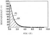
图4是示出在吸附判断工序中由直流电源向静电卡盘提供电力并向晶片提供电荷的情况下,由电压计所测量的施加给电阻的电压的推移的图表。FIG. 4 is a graph showing transition of a voltage applied to a resistor measured by a voltmeter when power is supplied to the electrostatic chuck and charges are supplied to the wafer from a DC power supply in the adsorption determination step.
图5是示出在借助晶片而使静电卡盘和搬送垫连接且直流电源不向静电卡盘提供电力的情况下,由电压计对施加给电阻的电压进行测量的状态的剖视图。5 is a cross-sectional view showing a state in which a voltage applied to a resistor is measured by a voltmeter when the electrostatic chuck and the transfer pad are connected via a wafer and the DC power supply does not supply power to the electrostatic chuck.
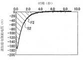
图6是示出在脱离判断工序中由电压计所测量的施加给电阻的电压的推移的图表。FIG. 6 is a graph showing transition of voltage applied to a resistor measured by a voltmeter in a detachment determination step.
标号说明Label description
1:减压处理装置;2:气体喷出头;20:轴承;21:气体扩散空间;21a:气体导入路;21b:气体喷出路;23:气缸;23a:缸筒;23b:活塞杆;23c:连结部件;25:反应气体提供源;27:匹配器;28:高频电源;3:静电卡盘;30:基轴部;30a:轴承;31:晶片保持部;31a:保持面;34:金属板;36:直流电源;37:第1配线;38:气压设备;38a:连通路;38b:分支路;39:冷却水提供构件;39a:冷却水通水路;6:减压室;62:搬入搬出口;62a:遮板;62b:遮板可动构件;64:减压构件;64a:排气口;7:搬送构件;70:搬送垫;700:吸附部;700a:保持面;701:框体;71:吸引源;71a:连通路;72:第2配线;79:臂部;790:连结部件;8:电压测量构件;80、81:电阻;84:电压计;9:控制部;91:第1判断构件;92:第2判断构件;W:晶片;Wa:晶片的正面;Wb:晶片的背面。1: Decompression treatment device; 2: Gas ejection head; 20: Bearing; 21: Gas diffusion space; 21a: Gas introduction path; 21b: Gas ejection path; 23: Cylinder; 23a: Cylinder barrel; 23b: Piston rod ;23c: connection member; 25: reaction gas supply source; 27: matcher; 28: high-frequency power supply; 3: electrostatic chuck; 30: base shaft; 30a: bearing; ;34: metal plate; 36: DC power supply; 37: first wiring; 38: air pressure equipment; 38a: connecting path; 38b: branch path; 39: cooling water supply component; Pressure chamber; 62: loading/unloading port; 62a: shutter; 62b: shutter movable member; 64: decompression member; 64a: exhaust port; 7: transfer member; 70: transfer pad; : Holding surface; 701: Housing; 71: Attraction source; 71a: Communication path; 72: Second wiring; 79: Arm; 790: Connection member; 8: Voltage measuring member; 80, 81: Resistance; Voltmeter; 9: control unit; 91: first judging means; 92: second judging means; W: wafer; Wa: front side of wafer; Wb: back side of wafer.
具体实施方式detailed description
在减压环境下对晶片W进行处理的图1所示的减压处理装置1例如是等离子蚀刻装置,其至少具有:静电卡盘3,其具有对晶片W进行保持的保持面31a;减压室6,其具有对配设有静电卡盘3的室内进行减压的减压构件64;以及搬送构件7,其相对于减压室6对晶片W进行搬入和搬出。另外,减压处理装置1并不限定于等离子蚀刻装置。The reduced-
静电卡盘3例如具有:基轴部30,其借助轴承30a以能够旋转的方式贯穿插入在减压室6的下部;晶片保持部31,其由氧化铝等陶瓷或氧化钛等电介质形成,其纵截面为大致T字状。例如形成为圆板状的晶片保持部31在基轴部30的上端侧与基轴部30一体形成,晶片保持部31的上表面是由电介质构成的对晶片W进行保持的保持面31a。另外,晶片保持部31也可以通过在其他的部件上配置由陶瓷等构成的电介质膜而构成。The
在基轴部30和晶片保持部31的内部形成有供冷却水通过的以虚线表示的冷却水通水路39a,冷却水通水路39a与冷却水提供构件39连通。冷却水提供构件39使冷却水流入冷却水通水路39a,该冷却水从内部对静电卡盘3进行冷却。例如,当在处理对象的晶片W上粘贴有未图示的保护带等的情况下,在等离子蚀刻处理中,能够通过冷却水提供构件39将静电卡盘3的保持面31a的温度保持在不从保护带产生气体的温度以下。A
在静电卡盘3的内部埋设有通过施加电压而产生电荷的作为电极的金属板34。金属板34形成为圆形板状,与保持面31a平行地配设,经由第1配线37而与直流电源36的正端子侧连接。通过从直流电源36对金属板34施加高压的直流电压,在保持面31a上产生因极化而出现的电荷(静电),通过其库仑力将晶片W静电吸附在保持面31a上。A
在基轴部30中如图1所示的那样形成有连通路38a,连通路38a的下端侧与由真空产生装置和压缩机等构成的气压设备38连通。气压设备38具有在保持面31a上产生吸引力的作为空气吸引源的功能和将空气提供到保持面31a上的作为空气提供源的功能的两种功能。连通路38a延伸到晶片保持部31,在晶片保持部31的内部分支成多个分支路38b。从连通路38a分支出的各分支路38b朝向厚度方向(Z轴方向)贯穿金属板34,各分支路38b的上端在静电卡盘3的保持面31a上开口。As shown in FIG. 1 , a
喷出反应气体的气体喷出头2借助轴承20而升降自如地配设在减压室6的上部。在气体喷出头2的内部设置有气体扩散空间21,气体扩散空间21的上部与气体导入路21a连通,气体扩散空间21的下部与气体喷出路21b连通。气体喷出路21b的下端在气体喷出头2的下表面朝向静电卡盘3侧开口。气体喷出头2与使气体喷出头2进行上下动作的气缸23连接。气缸23例如具有:缸筒23a,其固定在减压室6的上表面上,在缸筒23a的内部具有未图示的活塞,在缸筒23a的基端侧(-Z方向侧)具有底部;活塞杆23b,其插入到缸筒23a中且一端安装在活塞上;以及连结部件23c,其固定在活塞杆23b的另一端,对气体喷出头2进行支承。对缸筒23a提供(或排出)空气而使缸筒23a的内部的压力变化,从而活塞杆23b沿Z轴方向进行上下动作,气体喷出头2也随之进行上下动作。The gas ejection head 2 for ejecting the reaction gas is disposed on the upper portion of the decompression chamber 6 so as to be able to move up and down via
形成于气体喷出头2的内部的气体导入路21a与反应气体提供源25连通。反应气体提供源25例如对作为反应气体的SF6、CF4、C2F6、C2F4等氟类气体进行贮存。另外,除了反应气体提供源25之外,气体导入路21a也可以与贮存有对等离子蚀刻反应进行辅助的气体的未图示的辅助气体提供源连通。在该情况下,在辅助气体提供源中贮存有Ar、He等稀有气体来作为辅助气体。The
气体喷出头2经由匹配器27与高频电源28连接。通过从高频电源28经由匹配器27向气体喷出头2提供高频电力,能够使从气体喷出路21b喷出的气体等离子化。The gas ejection head 2 is connected to a high-frequency power supply 28 via a matching unit 27 . By supplying high-frequency power from the high-frequency power supply 28 to the gas discharge head 2 via the matching unit 27 , the gas discharged from the gas discharge passage 21 b can be plasmatized.
在减压室6的侧部设置有用于进行晶片W的搬入搬出的搬入搬出口62和对该搬入搬出口62进行开闭的遮板62a。例如,遮板62a能够通过气缸等遮板可动构件62b进行上下动作。A loading/unloading
在减压室6的下部形成有排气口64a,该排气口64a与减压构件64连接。通过使该减压构件64进行动作,能够将减压室6的内部减压到规定的真空度。An
构成图1所示的搬送构件7的搬送垫70例如其外形为圆形,具有:吸附部700,其由石墨多孔或金属多孔等导电体的多孔部件构成,对晶片W进行吸附;以及框体701,其对吸附部700进行支承。吸附部700与连通路71a的一端连通,连通路71a的另一端与由真空产生装置和压缩机等构成的吸引源71连接。并且,通过使吸引源71进行吸引来产生吸引力,该吸引力经由连通路71a传递到作为吸附部700的露出面的、与框体701的下表面形成为同一平面的具有导电性的保持面700a,由此,搬送垫70能够利用保持面700a对晶片W进行吸引保持。The
例如,在搬送垫70的框体701的上表面固定有连结部件790,搬送垫70借助连结部件790固定在臂部79的一端的下表面侧。臂部79能够在水平面上进行平行移动或旋转移动,并且能够沿Z轴方向进行上下动作。For example, a
搬送构件7具有将搬送垫70接地的第2配线72。第2配线72的一端72b接地,另一端72a与搬送垫70的吸附部700连接。The conveyance member 7 has a
如图1所示,在第2配线72上,电阻80与电阻81串联连接,并且,对电阻81的两端的电压进行测量的电压计84与电阻81并联连接。通过该电阻80和电阻81以及电压计84来构成电压测量构件8。另外,电压测量构件8的结构并不限定于本实施方式,例如,也可以具有电阻80和电阻81以外的电阻。并且,电阻80和电阻81以及电压计84也可以不与第2配线72连接,而如图2所示的那样与第1配线37连接。As shown in FIG. 1 , a
如图1所示,减压处理装置1具有由CPU和存储器等存储元件等构成的控制部9,在控制部9的控制下,对蚀刻气体的喷出量及时间、高频电力等条件进行控制。控制部9具有:第1判断部91,其对静电卡盘3的保持面31a是否吸附着晶片W进行判断;以及第2判断部92,其对晶片W是否从静电卡盘3的保持面31a脱离进行判断。将与电压计84所测量出的施加给电阻81的电压有关的信息发送给控制部9。As shown in FIG. 1 , the
以下,对使用图1所示的减压处理装置1在减压环境下对晶片W进行处理(在本实施方式中为等离子蚀刻处理)情况下的减压处理装置1的动作进行说明。晶片W例如是外形为圆形的半导体晶片,晶片的背面Wb成为实施等离子蚀刻处理的面。在晶片W的正面Wa上例如形成有多个器件。例如也可以通过粘贴未图示的保护带来保护晶片W的正面Wa。Next, the operation of the reduced-
通过臂部79来使搬送垫70在水平面上移动,将搬送垫70定位在晶片W的上方以使搬送垫70的中心与朝向上侧的状态的晶片W的背面Wb的中心大致一致。进而,臂部79朝向-Z方向下降,搬送垫70的保持面700a与晶片W的背面Wb接触。并且,通过使吸引源71进行吸引,如图1所示的那样搬送垫70利用保持面700a对晶片W进行吸引保持。The
接着,搬送构件7将晶片W搬入到减压室6内的静电卡盘3上。这里,通过实施对静电卡盘3是否吸附保持着晶片W进行确认的吸附确认方法,防止出现在静电卡盘3没有充分吸附晶片W的状态下进行晶片W的减压处理的情况。Next, the transport member 7 transports the wafer W onto the
(1)吸附确认方法中的连接工序(1) Connection process in the adsorption confirmation method
打开减压室6的遮板62a,使吸引保持着晶片W的搬送垫70通过搬入搬出口62而向静电卡盘3上移动。并且,使搬送垫70下降,使晶片W的正面Wa侧与静电卡盘3的保持面31a接触,将晶片W载置在静电卡盘3上。这样,如图3所示,借助晶片W而使静电卡盘3和搬送垫70连接。The
(2)吸附确认方法中的吸附判断工序(2) Adsorption determination process in the adsorption confirmation method
在实施了连接工序之后,如图3所示,接通直流电源36的开关360,从直流电源36经由第1配线37向静电卡盘3提供电力,对金属板34施加规定的直流电压(例如,5000V的直流电压)从而在金属板34上的晶片保持部31的电介质层与晶片W之间产生电介质极化现象。通过电介质极化现象将正(+)电荷集中在晶片保持部31的保持面31a附近。并且,由于静电卡盘3和搬送垫70成为借助晶片W而连接的状态,所以经由第2配线72和由导电体形成的吸附部700对晶片W提供负(-)电荷,从而使晶片W带负电。因此,通过在晶片W与保持面31a之间作用的静电力将晶片W吸附保持在保持面31a上。After performing the connection step, as shown in FIG. For example, a DC voltage of 5000 V) to generate a dielectric polarization phenomenon between the dielectric layer of the
这里,电压计84在电阻81的两端对向晶片W提供负(-)电荷时的施加给电压测量构件8的电阻81的电压(过度电压)进行测量。即,当从直流电源36经由第1配线37向静电卡盘3提供电力从而对电阻81施加直流电压时,在短时间内流过根据欧姆定律得到的直流电流。其结果是,电压计84所测量的施加给电阻81的电压例如如图4所示的曲线F1那样在大约0.3秒间从稳定电压0V急剧上升到过度电压(例如,170V)附近,之后逐渐下降,在大约3.7秒之后回到稳定电压。这里,从0秒时起到经过大约4.0秒时的曲线F1的积分值(在图4中以虚线示出的面积S1)表示晶片W的带电量。并且,如图4所示,当从直流电源36经由第1配线37向静电卡盘3提供电力时(0秒时)起到经过大约4秒的时间(即,晶片W的带电量变化的过度状态)时,晶片W变成充分带负电的稳定状态,电压计84所测量的施加给电阻81的电压也稳定在0V。并且,通过在晶片W与保持面31a之间作用的静电力,晶片W成为充分地吸附保持在保持面31a上的状态。Here, the
例如,在图1所示的控制部9的第1判断部91中存储有在静电卡盘3的保持面31a充分吸附着晶片W的情况下由电压计84所测量的施加给电阻81的电压的电压值(例如,170V)。存储在第1判断部91中的电压值的值按照每张晶片W的大小、厚度来确定,间接地示出了为了使晶片W充分地吸附于静电卡盘3而需要的晶片W的带电量。当接通直流电源36的开关360时,与电压计84所计测的施加给电阻81的电压的电压值有关的信息被随时发送给第1判断部91。并且,在从电压计84所测量的施加给电阻81的电压的电压值变为170V时起的例如大约3.7秒之后,第1判断部91判断为晶片W充分带负电,静电卡盘3利用保持面31a对晶片W进行充分地吸附保持。另一方面,在电压计84所测量的施加给电阻81的电压的电压值未达到170V的情况下,第1判断部91判断为晶片W的吸引保持不充分。例如,第1判断部91对作业者发送这一判断的结果。For example, the voltage applied to the
这样,本发明的吸附确认方法通过实施(1)连接工序和(2)吸附判断工序,即使在将晶片W搬入到减压处理装置1所具有的静电卡盘3上那样、很难由装置对静电卡盘3是否充分吸附着晶片W进行判断的情况下,也能够由装置容易地确认静电卡盘3是否充分吸附着晶片W。In this way, the adsorption confirmation method of the present invention implements (1) the connection step and (2) the adsorption determination step, so that even when the wafer W is loaded onto the
装置在确认了静电卡盘3充分吸附着晶片W之后,停止吸引源71所进行的吸引,使晶片W从搬送垫70的保持面700a离开。并且,搬送垫70从图1所示的减压室6内立即退回。利用遮板62a将减压室6的搬入搬出口62关闭,通过减压构件64对减压室6内进行减压排气而成为真空状态。另外,例如,气压设备38进行吸引而将残留在晶片W的正面Wa与静电卡盘3的保持面31a之间的空气吸引去除。并且,使图1所示的气体喷出头2下降,在该状态下向气体喷出头2内的气体导入路21a提供贮存在反应气体提供源25中的蚀刻气体(例如,SF6)。提供到气体导入路21a的蚀刻气体被各气体喷出路21b分流而从各气体喷出路21b的开口朝向吸附保持在静电卡盘3上的晶片W的背面Wb整个面均匀地喷出。After confirming that the
通过将蚀刻气体导入到减压室6内并且从高频电源28对气体喷出头2施加高频电力,在气体喷出头2与静电卡盘3之间产生高频电场,使蚀刻气体等离子化。等离子化后的蚀刻气体对晶片W的背面Wb进行蚀刻。另外,由于在静电卡盘3充分吸附着晶片W的状态下进行等离子蚀刻,所以不会产生电弧。By introducing etching gas into the decompression chamber 6 and applying high-frequency power to the gas ejection head 2 from the high-frequency power supply 28, a high-frequency electric field is generated between the gas ejection head 2 and the
在适当进行了晶片W的背面Wb的等离子蚀刻之后,停止对气体喷出头2的高频电力的施加,通过减压构件64将减压室6内的蚀刻气体从排气口64a排出,使减压室6的内部成为不存在蚀刻气体的状态。接着,打开搬入搬出口62的遮板62a而通过搬送构件7将晶片W从减压室6内的静电卡盘3搬出,此时实施对晶片W是否脱离静电卡盘3进行确认的脱离确认方法。其理由是为了防止在静电卡盘3没有充分解除晶片W的静电吸附的状态下进行搬送垫70对晶片W的吸引保持而使晶片W破损的情况。After the plasma etching of the back surface Wb of the wafer W is properly performed, the application of high-frequency power to the gas ejection head 2 is stopped, and the etching gas in the decompression chamber 6 is exhausted from the
(3)脱离确认方法中的连接工序(3) Connecting process in the detachment confirmation method
使图1所示的搬送垫70通过搬入搬出口62而移动到静电卡盘3所吸附保持的晶片W上,对搬送垫70和晶片W进行对位。并且,使搬送垫70下降而使晶片W的背面Wb与搬送垫70的保持面700a接触,借助晶片W而使静电卡盘3和搬送垫70连接。The
(4)脱离确认方法中的脱离判断工序(4) Detachment judgment process in the detachment confirmation method
在实施了连接工序之后,如图5所示断开直流电源36的开关360而停止从直流电源36向静电卡盘3的电力提供。由此,停止直流电源36对金属板34的直流电压的施加,但即使停止对金属板34的通电,晶片保持部31的保持面31a附近的电荷也不会立即消失,并且,晶片W的带电状态不会立即解除。因此,由于在保持面31a与晶片W之间残留有作为残留吸附力的静电力,所以不会立即变成晶片W从静电卡盘3充分脱离的状态。After the connection step is performed, the
在晶片W的带电被解除的状态下,电压计84在电阻81的两端对施加给电压测量构件8的电阻81的电压(过度电压)进行测量。电压计84所测量的施加给电阻81的电压例如如图6所示的曲线F2那样在大约0.3秒间从稳定电压0V例如急剧下降到作为过度电压的-170V附近,之后逐渐上升,在大约3.7秒后回到稳定电压。这里,从0秒时起到大约经过4秒时的曲线F2的积分值(在图6中以虚线示出的面积S2)表示晶片W所失去的电荷量。并且,如图6所示,当从断开直流电源36的开关360时(0秒时)起到经过大约4秒的时间(即,晶片W的带电量减少的过度状态)时,晶片W变成不带电的稳定状态,电压计84所测量的施加给电阻81的电压也稳定在0V。并且,在晶片W与保持面31a之间作用的静电力也消失,晶片W变成从晶片保持部31的保持面31a上充分脱离的状态。The
例如,在图1所示的控制部9的第2判断部92中存储有在能够判断为晶片W从静电卡盘3的保持面31a可靠地脱离的情况下的、由电压计84所测量的施加给电阻81的电压的电压值(例如,-170V)。存储在第2判断部92中的电压值的值按照每张晶片W的大小或厚度来确定,间接地示出了为了能够使晶片W从静电卡盘3可靠地脱离而需要的从晶片W去除的电荷量。当断开直流电源36的开关360时,与电压计84所计测的施加给电阻81的电压的电压值有关的信息被随时发送给第2判断部92。并且,在从电压计84所测量的施加给电阻81的电压的电压值变为-170V时起的例如大约3.7秒之后,第2判断部92判断为负电荷被从晶片W充分地去除,晶片W从静电卡盘3的保持面31a充分脱离。另一方面,在电压计84所测量的施加给电阻81的电压的电压值未达到-170V的情况下,第2判断部92判断为晶片W没有可靠地脱离。例如,第2判断部92对作业者发送本判断的结果。For example, the
这样,本发明的脱离确认方法通过实施(3)连接工序和(4)脱离判断工序,即使在将晶片W从减压处理装置1所具有的静电卡盘3搬出那样、很难由装置对晶片W是否从静电卡盘3充分脱离进行判断的情况下,也能够由装置容易地确认晶片W是否从静电卡盘3可靠地脱离。In this way, the detachment confirmation method of the present invention implements (3) the connection step and (4) the detachment determination step, so that even when the wafer W is unloaded from the
在装置确认了晶片W从静电卡盘3可靠地脱离之后,例如,气压设备38对静电卡盘3的保持面31a进行空气提供,通过空气的喷射压力将晶片W从保持面31a推起。这是为了排除静电卡盘3的保持面31a与晶片W之间的真空吸附力。并且,通过使图5所示的吸引源71进行吸引,搬送垫70利用保持面700a对晶片W进行吸引保持,将晶片W从静电卡盘3搬出。这里,由于静电卡盘3对晶片W的静电吸附被充分解除,所以即使使搬送垫70上升,晶片W也不会破损。After the device confirms that the wafer W is reliably detached from the
另外,本发明的减压处理装置1并不限定于上述实施方式,并且,附图中图示的各结构的大小或形状等也并不限定于此,能够在可以发挥本发明的效果的范围内进行适当变更。例如,在将保护带粘贴在晶片上并使保护带侧与静电卡盘接触而利用保持面进行保持时,由于将保护带作为电介质,所以也可以使埋设在静电卡盘中的金属板在保持面露出。In addition, the
Claims (3)
Applications Claiming Priority (2)
| Application Number | Priority Date | Filing Date | Title |
|---|---|---|---|
| JP2016142216AJP6697346B2 (en) | 2016-07-20 | 2016-07-20 | Adsorption confirmation method, desorption confirmation method, and decompression treatment device |
| JP2016-142216 | 2016-07-20 |
Publications (2)
| Publication Number | Publication Date |
|---|---|
| CN107644830A CN107644830A (en) | 2018-01-30 |
| CN107644830Btrue CN107644830B (en) | 2022-12-20 |
Family
ID=60990106
Family Applications (1)
| Application Number | Title | Priority Date | Filing Date |
|---|---|---|---|
| CN201710584227.9AActiveCN107644830B (en) | 2016-07-20 | 2017-07-18 | Wafer adsorption confirmation method, detachment confirmation method, and reduced-pressure processing apparatus |
Country Status (6)
| Country | Link |
|---|---|
| US (1) | US10910246B2 (en) |
| JP (1) | JP6697346B2 (en) |
| KR (1) | KR102174879B1 (en) |
| CN (1) | CN107644830B (en) |
| SG (1) | SG10201705680XA (en) |
| TW (1) | TWI727055B (en) |
Families Citing this family (15)
| Publication number | Priority date | Publication date | Assignee | Title |
|---|---|---|---|---|
| JP6905382B2 (en)* | 2017-04-14 | 2021-07-21 | 株式会社ディスコ | Wafer loading / unloading method |
| US10825645B2 (en)* | 2017-08-17 | 2020-11-03 | Varian Semiconductor Equipment Associates, Inc. | System and method for reduced workpiece adhesion due to electrostatic charge during removal from a processing station |
| KR102516885B1 (en)* | 2018-05-10 | 2023-03-30 | 삼성전자주식회사 | Deposition equipment and method of fabricating semiconductor device using the same |
| JP7333346B2 (en)* | 2018-06-08 | 2023-08-24 | アプライド マテリアルズ インコーポレイテッド | Apparatus for suppressing parasitic plasma in plasma-enhanced chemical vapor deposition chamber |
| JP7052584B2 (en)* | 2018-06-15 | 2022-04-12 | 東京エレクトロン株式会社 | Plasma processing equipment and plasma processing method |
| JP6913060B2 (en)* | 2018-07-24 | 2021-08-04 | 株式会社日立ハイテク | Plasma processing equipment and plasma processing method |
| JP2020038907A (en)* | 2018-09-04 | 2020-03-12 | 株式会社ディスコ | Plasma processing equipment |
| JP7188992B2 (en)* | 2018-11-27 | 2022-12-13 | 株式会社ディスコ | Plasma etching equipment |
| JP7696840B2 (en)* | 2019-06-07 | 2025-06-23 | アプライド マテリアルズ インコーポレイテッド | Seamless wire conduit |
| JP7451028B2 (en)* | 2019-12-27 | 2024-03-18 | 株式会社ディスコ | How to place the protective sheet |
| CN114613657A (en) | 2020-12-09 | 2022-06-10 | 细美事有限公司 | Control program, container, and semiconductor element manufacturing equipment for charging and automatic calibration of wafer-type sensors |
| JP7652484B2 (en)* | 2021-03-08 | 2025-03-27 | 東京エレクトロン株式会社 | SUBSTRATE PROCESSING APPARATUS AND ABNORMALITY DETECTION METHOD |
| US20220356027A1 (en)* | 2021-05-04 | 2022-11-10 | Applied Materials, Inc. | Roller for transporting a flexible substrate, vacuum processing apparatus, and methods therefor |
| JP7675051B2 (en)* | 2022-06-29 | 2025-05-12 | 東京エレクトロン株式会社 | Plasma processing apparatus and plasma processing method |
| WO2024225020A1 (en)* | 2023-04-27 | 2024-10-31 | 株式会社クリエイティブテクノロジー | Workpiece holding device |
Citations (6)
| Publication number | Priority date | Publication date | Assignee | Title |
|---|---|---|---|---|
| JPH06291174A (en)* | 1993-04-06 | 1994-10-18 | Fuji Electric Co Ltd | Electrostatic chuck, and method for adhering and holding semiconductor wafer to electrostatic chuck |
| JPH09120988A (en)* | 1995-08-24 | 1997-05-06 | Tokyo Electron Ltd | Plasma processing method |
| US6238160B1 (en)* | 1998-12-02 | 2001-05-29 | Taiwan Semiconductor Manufacturing Company, Ltd' | Method for transporting and electrostatically chucking a semiconductor wafer or the like |
| JP2005064234A (en)* | 2003-08-12 | 2005-03-10 | Disco Abrasive Syst Ltd | Plasma etching method and plasma etching apparatus |
| JP2006202939A (en)* | 2005-01-20 | 2006-08-03 | Mitsubishi Heavy Ind Ltd | Attraction method, releasing method, plasma processing method, electrostatic chuck, and plasma processing apparatus |
| JP2008028021A (en)* | 2006-07-19 | 2008-02-07 | Disco Abrasive Syst Ltd | Plasma etching apparatus and plasma etching method |
Family Cites Families (12)
| Publication number | Priority date | Publication date | Assignee | Title |
|---|---|---|---|---|
| JPS63139634A (en)* | 1986-11-29 | 1988-06-11 | Tokuda Seisakusho Ltd | electrostatic chuck |
| JP2867526B2 (en)* | 1990-01-16 | 1999-03-08 | 富士通株式会社 | Semiconductor manufacturing equipment |
| JPH06224286A (en)* | 1993-01-26 | 1994-08-12 | Hitachi Ltd | Attraction monitoring device of electrostatic attraction apparatus |
| JP3373762B2 (en)* | 1997-08-22 | 2003-02-04 | 株式会社日立製作所 | Electrostatic suction device and electron beam lithography device using the same |
| JP3633854B2 (en) | 2000-06-12 | 2005-03-30 | 株式会社ディスコ | Semiconductor wafer processing equipment |
| US7535688B2 (en)* | 2005-03-25 | 2009-05-19 | Tokyo Electron Limited | Method for electrically discharging substrate, substrate processing apparatus and program |
| JP4699061B2 (en)* | 2005-03-25 | 2011-06-08 | 東京エレクトロン株式会社 | Substrate removal method, substrate processing apparatus, program |
| JP2007281007A (en)* | 2006-04-03 | 2007-10-25 | Nikon Corp | Substrate transport method, substrate transport apparatus, and exposure apparatus |
| US7750645B2 (en)* | 2007-08-15 | 2010-07-06 | Applied Materials, Inc. | Method of wafer level transient sensing, threshold comparison and arc flag generation/deactivation |
| KR101127165B1 (en)* | 2010-04-23 | 2012-03-20 | 청진테크 주식회사 | A leakage current monitoring apparatus for an electrostatic chuck system |
| JP5592833B2 (en)* | 2011-05-20 | 2014-09-17 | 株式会社日立ハイテクノロジーズ | Charged particle beam device and electrostatic chuck device |
| JP6649689B2 (en)* | 2015-03-16 | 2020-02-19 | 株式会社ディスコ | Decompression processing apparatus and wafer holding method |
- 2016
- 2016-07-20JPJP2016142216Apatent/JP6697346B2/enactiveActive
- 2017
- 2017-06-09TWTW106119312Apatent/TWI727055B/enactive
- 2017-06-30KRKR1020170083144Apatent/KR102174879B1/enactiveActive
- 2017-07-11SGSG10201705680XApatent/SG10201705680XA/enunknown
- 2017-07-13USUS15/648,663patent/US10910246B2/enactiveActive
- 2017-07-18CNCN201710584227.9Apatent/CN107644830B/enactiveActive
Patent Citations (6)
| Publication number | Priority date | Publication date | Assignee | Title |
|---|---|---|---|---|
| JPH06291174A (en)* | 1993-04-06 | 1994-10-18 | Fuji Electric Co Ltd | Electrostatic chuck, and method for adhering and holding semiconductor wafer to electrostatic chuck |
| JPH09120988A (en)* | 1995-08-24 | 1997-05-06 | Tokyo Electron Ltd | Plasma processing method |
| US6238160B1 (en)* | 1998-12-02 | 2001-05-29 | Taiwan Semiconductor Manufacturing Company, Ltd' | Method for transporting and electrostatically chucking a semiconductor wafer or the like |
| JP2005064234A (en)* | 2003-08-12 | 2005-03-10 | Disco Abrasive Syst Ltd | Plasma etching method and plasma etching apparatus |
| JP2006202939A (en)* | 2005-01-20 | 2006-08-03 | Mitsubishi Heavy Ind Ltd | Attraction method, releasing method, plasma processing method, electrostatic chuck, and plasma processing apparatus |
| JP2008028021A (en)* | 2006-07-19 | 2008-02-07 | Disco Abrasive Syst Ltd | Plasma etching apparatus and plasma etching method |
Also Published As
| Publication number | Publication date |
|---|---|
| JP6697346B2 (en) | 2020-05-20 |
| CN107644830A (en) | 2018-01-30 |
| JP2018014383A (en) | 2018-01-25 |
| TW201812966A (en) | 2018-04-01 |
| KR20180010133A (en) | 2018-01-30 |
| TWI727055B (en) | 2021-05-11 |
| US10910246B2 (en) | 2021-02-02 |
| US20180025928A1 (en) | 2018-01-25 |
| SG10201705680XA (en) | 2018-02-27 |
| KR102174879B1 (en) | 2020-11-05 |
Similar Documents
| Publication | Publication Date | Title |
|---|---|---|
| CN107644830B (en) | Wafer adsorption confirmation method, detachment confirmation method, and reduced-pressure processing apparatus | |
| KR102444698B1 (en) | Method of carrying out wafer | |
| JP4013753B2 (en) | Semiconductor wafer cutting method | |
| JP4786693B2 (en) | Wafer bonding apparatus and wafer bonding method | |
| JP5331500B2 (en) | Wafer processing method | |
| CN106340483B (en) | Chuck table and cleaning device | |
| JP6076063B2 (en) | Processing equipment | |
| KR101372805B1 (en) | Wafer etching process and using the same wafer etching system | |
| JP2003124612A (en) | Low pressure plasma processing apparatus and method | |
| TW202326879A (en) | Processing system, electrostatic carrier, and processing method | |
| JP7189722B2 (en) | Wafer transfer device and transfer method | |
| US12243848B2 (en) | Methods and systems for improving fusion bonding | |
| JP2008028021A (en) | Plasma etching apparatus and plasma etching method | |
| JP3948325B2 (en) | Film substrate processing method | |
| JP4245868B2 (en) | Method for reusing substrate mounting member, substrate mounting member and substrate processing apparatus | |
| JP2007258636A (en) | Dry etching method and apparatus | |
| TWI843824B (en) | Electrostatic adsorption device and static removal method | |
| KR100500471B1 (en) | De-chucking apparatus of electrostatic chuck for semiconductor equipment | |
| JP2019220634A (en) | Conveying method for work piece | |
| WO2024070009A1 (en) | Electrostatic carrier, treatment system, and treatment method | |
| JP4781833B2 (en) | Etching device | |
| JPS6349752B2 (en) | ||
| KR20090044868A (en) | Plasma Treatment Method |
Legal Events
| Date | Code | Title | Description |
|---|---|---|---|
| PB01 | Publication | ||
| PB01 | Publication | ||
| SE01 | Entry into force of request for substantive examination | ||
| SE01 | Entry into force of request for substantive examination | ||
| GR01 | Patent grant | ||
| GR01 | Patent grant |