CN107591444B - Enhancement transistor and method of making the same - Google Patents
Enhancement transistor and method of making the sameDownload PDFInfo
- Publication number
- CN107591444B CN107591444BCN201610532567.2ACN201610532567ACN107591444BCN 107591444 BCN107591444 BCN 107591444BCN 201610532567 ACN201610532567 ACN 201610532567ACN 107591444 BCN107591444 BCN 107591444B
- Authority
- CN
- China
- Prior art keywords
- layer
- thin film
- film layer
- mobility thin
- mode transistor
- Prior art date
- Legal status (The legal status is an assumption and is not a legal conclusion. Google has not performed a legal analysis and makes no representation as to the accuracy of the status listed.)
- Active
Links
Images


Landscapes
- Thin Film Transistor (AREA)
- Junction Field-Effect Transistors (AREA)
Abstract
Translated fromChinese
Description
Translated fromChinese技术领域technical field
本发明属于半导体技术领域,具体地讲,涉及一种增强型晶体管及其制作方法。The invention belongs to the technical field of semiconductors, and in particular, relates to an enhancement mode transistor and a manufacturing method thereof.
背景技术Background technique
近五十多年来,功率器件已经由第一代Si半导体材料发展到第二代GaAs半导体材料,再到目前的第三代SiC/GaN半导体材料。第一代Si半导体功率器件虽然取得了显著的成效,但目前其性能已经接近材料的理论极限,另外随着对频率和功率要求越来越高,第二代GaAs半导体材料由于其禁带宽度窄、击穿电场低等因素,导致GaAs功率器件不能满足现有的技术发展。作为重要的第三代宽禁带半导体材料,氮化镓(GaN)禁带宽度大(3.4eV)、击穿电场高(>3MV/cm),AlGaN/GaN异质结的二维电子气浓度高(>1013cm-2)、电子饱和漂移速度高(2.8×107cm/s),且GaN材料的化学惰性和高温稳定性好。因此,AlGaN/GaN高电子迁移率晶体管(HEMT)能够获得很高的击穿电压、功率密度以及极高的工作频率,且开关损耗非常小。Over the past fifty years, power devices have developed from the first generation of Si semiconductor materials to the second generation of GaAs semiconductor materials, and then to the current third generation of SiC/GaN semiconductor materials. Although the first-generation Si semiconductor power devices have achieved remarkable results, their performance is currently close to the theoretical limit of the material. In addition, with the increasing requirements for frequency and power, the second-generation GaAs semiconductor material has a narrow band gap due to its narrow band gap. , low breakdown electric field and other factors, resulting in GaAs power devices can not meet the existing technical development. As an important third-generation wide-bandgap semiconductor material, gallium nitride (GaN) has a large band gap (3.4eV), a high breakdown electric field (>3MV/cm), and the two-dimensional electron gas concentration of AlGaN/GaN heterojunctions High (>1013 cm-2 ), high electron saturation drift velocity (2.8×107 cm/s), and the GaN material has good chemical inertness and high temperature stability. Therefore, AlGaN/GaN high electron mobility transistors (HEMTs) can achieve high breakdown voltage, power density, and extremely high operating frequency with very small switching losses.
对于GaN材料的晶体管,目前最大的技术难题就是增强型(或常关型)器件的解决方案。由于极化效应的作用,AlGaN/GaN HEMT器件天然形成的是耗尽型的器件,一般需要对栅下的AlGaN等势垒层进行刻蚀,通过消除栅下的极化效应来实现常关型。另一方案是在表面增加一层p型GaN或p型AlGaN,通过能带将2DEG耗尽,但是需要对栅以外的几十纳米厚度的p型GaN或p型AlGaN进行刻蚀,这两种方案都面临刻蚀的均匀性、重复性和引入损伤等问题。还有一种方案是在栅下的AlGaN势垒中注入F离子,通过抬高栅下的能带耗尽2DEG,但是这种方案面临F离子的迁移而产生的高温和长期可靠性问题。此外,这三种方案都会对栅下的电子迁移率造成影响,使栅下迁移率大幅度下降,并且工艺复杂,成本较高。For transistors made of GaN materials, the biggest technical challenge at present is the solution of enhancement-mode (or normally-off) devices. Due to the polarization effect, AlGaN/GaN HEMT devices are naturally depleted devices. Generally, the barrier layer such as AlGaN under the gate needs to be etched, and the normally-off type is realized by eliminating the polarization effect under the gate. . Another solution is to add a layer of p-type GaN or p-type AlGaN on the surface to deplete the 2DEG through the energy band, but it needs to etch p-type GaN or p-type AlGaN with a thickness of tens of nanometers outside the gate. The solutions all face the problems of etching uniformity, repeatability and introduction of damage. Another solution is to implant F ions into the AlGaN barrier under the gate to deplete the 2DEG by raising the energy band under the gate, but this solution faces high temperature and long-term reliability problems caused by the migration of F ions. In addition, these three schemes will affect the electron mobility under the gate, so that the mobility under the gate is greatly reduced, and the process is complicated and the cost is high.
电子迁移率是影响功率器件工作频率的重要因素,高迁移率薄膜的制备和应用成为当前的研究热点并具有非常大的应用优势,石墨烯等材料的出现和成功制备为各领域的发展注入了新的活力,其非常突出的一个优势是具有非常高的载流子迁移率(室温下可超过200,000cm2/Vs),远远超过GaN等材料。石墨烯,尤其单层石墨烯可以制作工作频率极高的器件,从而降低开关损耗,缩小整个电子系统的体积。但受到石墨烯本身材料的限制,并不适合制作高功率和高耐压器件。Electron mobility is an important factor affecting the operating frequency of power devices. The preparation and application of high-mobility thin films has become a current research hotspot and has great application advantages. The emergence and successful preparation of graphene and other materials have injected a lot of The new vitality, one of its very prominent advantages is that it has a very high carrier mobility (over 200,000 cm2 /Vs at room temperature), far exceeding materials such as GaN. Graphene, especially single-layer graphene, can make devices with extremely high operating frequencies, thereby reducing switching losses and reducing the size of the entire electronic system. However, due to the limitation of graphene itself, it is not suitable for making high-power and high-voltage devices.
对于GaN材料的晶体管,电子迁移率约为2000cm2/V·s,远低于石墨烯或其他高迁移率薄膜材料的电子迁移率。对于石墨烯或其他高迁移率薄膜材料晶体管,由于单层石墨烯等没有带隙,所以无法实现关断,即使将栅下的石墨烯等材料刻蚀掉,采用类似Si基MOSFET的反型原理来实现关断,也会由于栅下的迁移率很低无法实现高迁移率的晶体管,无法发挥石墨烯等材料的高迁移率的优势。For transistors made of GaN materials, the electron mobility is about 2000 cm2 /V·s, which is much lower than that of graphene or other high-mobility thin-film materials. For graphene or other high-mobility thin-film material transistors, since single-layer graphene has no band gap, it cannot be turned off. Even if the graphene and other materials under the gate are etched away, the inversion principle similar to Si-based MOSFET is adopted. To achieve turn-off, due to the low mobility under the gate, high mobility transistors cannot be realized, and the advantages of high mobility of materials such as graphene cannot be exploited.
发明内容SUMMARY OF THE INVENTION
为了解决上述现有技术存在的问题,本发明提供一种增强型晶体管及其制作方法,能够提高电子迁移率、降低导通电阻、提升工作频率以及降低导通损耗和开关损耗,而且还能够降低了制作的复杂性和成本。In order to solve the above-mentioned problems in the prior art, the present invention provides an enhancement mode transistor and a manufacturing method thereof, which can improve electron mobility, reduce on-resistance, increase operating frequency, reduce conduction loss and switching loss, and also reduce complexity and cost of production.
本发明提出的具体技术方案为:提供一种增强型晶体管,包括衬底以及依次形成于所述衬底上的背势垒层、沟道层和异质层,所述异质层上设置有一高迁移率薄膜层,所述高迁移率薄膜层定义出源极区、漏极区和栅极区,所述源极区和漏极区分别连接有源电极和漏电极,所述栅极区被刻蚀形成一暴露出所述异质层的窗口;所述高迁移率薄膜层上依次形成有绝缘介质层和栅电极,所述栅电极在所述高迁移率薄膜层上的投影至少完全覆盖所述窗口。The specific technical scheme proposed by the present invention is to provide an enhancement mode transistor, which includes a substrate, a back barrier layer, a channel layer and a heterogeneous layer sequentially formed on the substrate, and a heterogeneous layer is provided on the heterogeneous layer. a high mobility thin film layer, the high mobility thin film layer defines a source region, a drain region and a gate region, the source region and the drain region are respectively connected to a source electrode and a drain electrode, the gate region is etched to form a window exposing the heterogeneous layer; an insulating dielectric layer and a gate electrode are sequentially formed on the high mobility thin film layer, and the projection of the gate electrode on the high mobility thin film layer is at least completely cover the window.
进一步地,所述高迁移率薄膜层的材质为石墨烯、二硫化钼或黑磷;和/或所述高迁移率薄膜层的厚度为0.1~3纳米。Further, the material of the high mobility thin film layer is graphene, molybdenum disulfide or black phosphorus; and/or the thickness of the high mobility thin film layer is 0.1-3 nanometers.
进一步地,所述异质层包括依次位于所述沟道层上的界面层和盖帽层。Further, the hetero layer includes an interface layer and a cap layer which are sequentially located on the channel layer.
进一步地,所述异质层的厚度为2~7纳米。Further, the thickness of the heterogeneous layer is 2-7 nanometers.
进一步地,所述盖帽层的厚度为1~5纳米;和/或所述界面层的厚度为1~2纳米。Further, the thickness of the cap layer is 1-5 nanometers; and/or the thickness of the interface layer is 1-2 nanometers.
进一步地,所述异质层的厚度为2.5~3.5纳米。Further, the thickness of the heterogeneous layer is 2.5-3.5 nanometers.
进一步地,所述衬底的材质为氮化镓,和/或所述背势垒层的材质为氮化铝镓,和/或所述沟道层的材质为氮化镓,和/或所述界面层的材质为氮化铝,和/或所述盖帽层的材质为氮化镓。Further, the material of the substrate is gallium nitride, and/or the material of the back barrier layer is aluminum gallium nitride, and/or the material of the channel layer is gallium nitride, and/or the material of the channel layer is gallium nitride. The material of the interface layer is aluminum nitride, and/or the material of the capping layer is gallium nitride.
本发明还提供一种如上所述的增强型晶体管的制作方法,包括步骤:The present invention also provides a method for fabricating the enhancement mode transistor as described above, comprising the steps of:
提供一衬底并在所述衬底上依次生长形成背势垒层、沟道层和异质层;providing a substrate and sequentially growing on the substrate to form a back barrier layer, a channel layer and a heterolayer;
在所述异质层上生长形成高迁移率薄膜层;growing on the heterogeneous layer to form a high mobility thin film layer;
在所述高迁移率薄膜层上应用刻蚀工艺制备形成一窗口;Applying an etching process to prepare a window on the high mobility thin film layer;
在所述高迁移率薄膜层上分别沉积源电极、漏电极以及绝缘介质层;respectively depositing a source electrode, a drain electrode and an insulating medium layer on the high mobility thin film layer;
在所述绝缘介质层上对应于所述窗口的位置沉积形成栅电极,所述栅电极在所述高迁移率薄膜层上的投影至少完全覆盖所述窗口。A gate electrode is deposited on the insulating medium layer at a position corresponding to the window, and the projection of the gate electrode on the high-mobility thin film layer at least completely covers the window.
进一步地,生长形成所述高迁移率薄膜层所应用的工艺为化学气相沉积工艺或机械剥离转移工艺。Further, the process used to grow and form the high mobility thin film layer is a chemical vapor deposition process or a mechanical lift-off transfer process.
进一步地,所述刻蚀工艺为氧等离子体刻蚀或反应离子刻蚀或离子束刻蚀。Further, the etching process is oxygen plasma etching or reactive ion etching or ion beam etching.
本发明提供的增强型晶体管及其制作方法,在绝缘介质层与盖帽层之间形成有高迁移率薄膜层,提升了整个增强型晶体管的电子迁移率和工作频率、降低了整个增强型晶体管的导通损耗和开关损耗;而且,高迁移率薄膜层刻蚀形成有与栅电极对应的窗口,使得晶体管能够实现增强型工作模式。此外,本发明提供的增强型晶体管及其制作方法不需要对栅下和栅以外区域进行刻蚀,避免因刻蚀工艺引入的均匀性、重复性和引入损伤问题,简化了制作工艺及晶体管的结构,降低了制作成本。In the enhancement mode transistor and the manufacturing method thereof provided by the present invention, a high-mobility thin film layer is formed between the insulating medium layer and the cap layer, which improves the electron mobility and operating frequency of the entire enhancement mode transistor, and reduces the entire enhancement mode transistor. conduction loss and switching loss; and, the high mobility thin film layer is etched to form a window corresponding to the gate electrode, so that the transistor can realize an enhancement mode of operation. In addition, the enhancement mode transistor and its manufacturing method provided by the present invention do not need to etch the regions under the gate and outside the gate, avoiding the problems of uniformity, repeatability and damage introduced by the etching process, and simplifying the manufacturing process and transistor performance. structure, reducing the production cost.
附图说明Description of drawings
通过结合附图进行的以下描述,本发明的实施例的上述和其它方面、特点和优点将变得更加清楚,附图中:The above and other aspects, features and advantages of embodiments of the present invention will become more apparent from the following description taken in conjunction with the accompanying drawings, in which:
图1为本发明增强型晶体管的结构示意图;1 is a schematic structural diagram of an enhancement mode transistor of the present invention;
图2a至图2f为本发明增强型晶体管的制作流程图。2a to 2f are the flow charts of the fabrication of the enhancement mode transistor of the present invention.
具体实施方式Detailed ways
以下,将参照附图来详细描述本发明的实施例。然而,可以以许多不同的形式来实施本发明,并且本发明不应该被解释为限制于这里阐述的具体实施例。相反,提供这些实施例是为了解释本发明的原理及其实际应用,从而使本领域的其他技术人员能够理解本发明的各种实施例和适合于特定预期应用的各种修改。Hereinafter, embodiments of the present invention will be described in detail with reference to the accompanying drawings. The present invention may, however, be embodied in many different forms and should not be construed as limited to the specific embodiments set forth herein. Rather, these embodiments are provided to explain the principles of the invention and its practical application, to thereby enable others skilled in the art to understand the invention for various embodiments and with various modifications as are suited to the particular intended use.
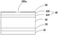
参照图1,本实施例提供的增强型晶体管包括衬底10以及依次形成于所述衬底10上的背势垒层20、沟道层30和异质层40,所述异质层40上设置有一高迁移率薄膜层50,所述高迁移率薄膜层50定义出源极区501、漏极区502和栅极区503,所述源极区501和漏极区502分别连接有源电极100和漏电极101,所述栅极区503被刻蚀形成一暴露出所述异质层40的窗口503a;所述高迁移率薄膜层50上依次形成有绝缘介质层60和栅电极102,所述栅电极102在所述高迁移率薄膜层50上的投影至少完全覆盖所述窗口503a。Referring to FIG. 1 , the enhancement mode transistor provided in this embodiment includes a
所述衬底10作为整个增强型晶体管的基板,其材质为氮化镓。背势垒层20的材质为氮化铝镓,沟道层30的材质为氮化镓。源电极100、漏电极101以及栅电极102作为整个增强型晶体管的接触电极,源电极100、漏电极101以及栅电极102的材质为金属。高迁移率薄膜层50的材质为石墨烯、二硫化钼或黑磷,优选的,高迁移率薄膜层50的材质为石墨烯,其中,高迁移率薄膜层的厚度为0.1~3纳米。当加载在源电极100以及栅电极102之间的电压小于增强型晶体管的开启电压时,异质层40与沟道层30的界面处不存在电子,增强型晶体管处于关断状态;当加载在源电极100以及栅电极102之间的电压大于增强型晶体管的开启电压时,异质层40与沟道层30的界面处存在二维电子气(2DEG),高迁移率薄膜层50以及二维电子气(2DEG)组成电子运输通道,此时,增强型晶体管处于导通状态。The
具体的,异质层40的厚度为2~7纳米,优选的,异质层40的厚度为2.5~3.5纳米。其中,异质层40包括依次位于沟道层30上的界面层410以及盖帽层420,盖帽层420的厚度为1~5纳米,界面层230的厚度为1~2纳米。界面层230的材质为氮化铝,盖帽层420的材质为氮化镓。由于异质层40的厚度很薄,从而保证了高迁移率薄膜层50的电子波函数与二维电子气(2DEG)电子波函数的耦合。Specifically, the thickness of the
参照图2a~图2f所示,本实施例还提供了上述增强型晶体管的制作方法,具体包括以下步骤:Referring to FIGS. 2a-2f, the present embodiment also provides a method for fabricating the enhancement mode transistor, which specifically includes the following steps:
步骤S1、提供一衬底10并在衬底10上依次生长形成背势垒层20、沟道层30和异质层40,其中,生长所采用的工艺为金属有机化学气相沉积(MOCVD)或分子束外延(MBE)或氢化物气相外延(HVPE),也可以采用其他外延技术(如图2a所示)。Step S1, providing a
具体的,步骤S1包括依次在衬底10上生长形成背势垒层20、沟道层30、界面层410以及盖帽层420。Specifically, step S1 includes sequentially growing and forming a
步骤S2、在异质层40上生长形成高迁移率薄膜层50,具体的,在盖帽层420上生长形成高迁移率薄膜层50。其中,生长形成高迁移率薄膜层50采用的工艺为化学气相沉积(CVD)或机械剥离转移工艺,当然也可以采用本领域技术人员所熟知的其他工艺,这里不做限定。(如图2b所示)。Step S2 , growing and forming the high mobility
步骤S3、在高迁移率薄膜层50上应用刻蚀工艺制备形成一窗口503a,其中,刻蚀工艺采用的是氧等离子体或反应离子刻蚀或离子束刻蚀(如图2c所示)。Step S3, applying an etching process to form a
步骤S4、在高迁移率薄膜层50上分别沉积源电极100、漏电极101以及绝缘介质层60,其中,沉积源电极100和漏电极101采用的工艺为电子束蒸发或溅射,也可以采用其他金属沉积技术(如图2d所示);沉积绝缘介质层60采用的工艺为原子层沉积(ALD)或化学气相沉积,也可以采用其他介质层沉积技术(如图2e所示)。Step S4 , depositing the
步骤S5、在绝缘介质层60上对应于窗口503a的位置沉积形成栅电极102,所述栅电极102在高迁移率薄膜层50上的投影至少完全覆盖窗口503a,其中,沉积栅电极102的工艺为电子束蒸发或溅射,也可以采用其他金属沉积技术(如图2f所示)。Step S5, depositing a
本发明提供的增强型晶体管及其制作方法,在绝缘介质层60与盖帽层420之间形成有高迁移率薄膜层50,采用石墨烯或其他高迁移率薄膜作为沟道的一部分,大幅度提高器件的电子迁移率,进而降低了整体器件的导通电阻,提升了整个增强型晶体管的电子迁移率和工作频率、降低了整个增强型晶体管的导通损耗和开关损耗;而且,高迁移率薄膜层50刻蚀形成有与栅电极102对应的窗口,使得晶体管能够实现增强型工作模式。此外,本发明提供的增强型晶体管及其制作方法不需要对异质层40进行刻蚀,避免因刻蚀工艺引入的均匀性、重复性和引入损伤问题,器件的整体结构生长得到简化并减少了刻蚀或离子注入等工艺,简化了制作工艺及晶体管的结构,降低了制作成本。In the enhancement mode transistor and the manufacturing method thereof provided by the present invention, a high-mobility
虽然已经参照特定实施例示出并描述了本发明,但是本领域的技术人员将理解:在不脱离由权利要求及其等同物限定的本发明的精神和范围的情况下,可在此进行形式和细节上的各种变化。While the invention has been shown and described with reference to specific embodiments, those skilled in the art will appreciate that forms and Various changes in details.
Claims (10)
Priority Applications (1)
| Application Number | Priority Date | Filing Date | Title |
|---|---|---|---|
| CN201610532567.2ACN107591444B (en) | 2016-07-08 | 2016-07-08 | Enhancement transistor and method of making the same |
Applications Claiming Priority (1)
| Application Number | Priority Date | Filing Date | Title |
|---|---|---|---|
| CN201610532567.2ACN107591444B (en) | 2016-07-08 | 2016-07-08 | Enhancement transistor and method of making the same |
Publications (2)
| Publication Number | Publication Date |
|---|---|
| CN107591444A CN107591444A (en) | 2018-01-16 |
| CN107591444Btrue CN107591444B (en) | 2020-12-22 |
Family
ID=61045636
Family Applications (1)
| Application Number | Title | Priority Date | Filing Date |
|---|---|---|---|
| CN201610532567.2AActiveCN107591444B (en) | 2016-07-08 | 2016-07-08 | Enhancement transistor and method of making the same |
Country Status (1)
| Country | Link |
|---|---|
| CN (1) | CN107591444B (en) |
Families Citing this family (4)
| Publication number | Priority date | Publication date | Assignee | Title |
|---|---|---|---|---|
| CN111446289B (en)* | 2020-04-09 | 2020-11-20 | 浙江大学 | Structure of GaN device based on graphene capping layer and preparation method thereof |
| CN112259604B (en)* | 2020-10-16 | 2023-05-02 | 南京南智先进光电集成技术研究院有限公司 | Gallium nitride composite substrate, gallium nitride device and preparation method of gallium nitride composite substrate |
| CN114203804B (en)* | 2021-11-19 | 2024-11-26 | 西安瑞芯光通信息科技有限公司 | A HEMT chip of silicon carbide-based graphene material and preparation method thereof |
| CN116705847A (en)* | 2023-05-31 | 2023-09-05 | 河源市众拓光电科技有限公司 | Low-loss HEMT device and preparation method thereof |
Citations (5)
| Publication number | Priority date | Publication date | Assignee | Title |
|---|---|---|---|---|
| JP2008141040A (en)* | 2006-12-04 | 2008-06-19 | Nec Corp | Field effect transistor and method of manufacturing the same |
| CN102427085A (en)* | 2011-11-18 | 2012-04-25 | 中国科学院苏州纳米技术与纳米仿生研究所 | Group III nitride enhancement mode HEMT (High Electron Mobility Transistor) device |
| CN102479804A (en)* | 2010-11-30 | 2012-05-30 | 三星电子株式会社 | Graphene electronics |
| CN102789982A (en)* | 2011-05-16 | 2012-11-21 | 中国科学院微电子研究所 | Enhanced AlN/GaN high electron mobility transistor and manufacturing method thereof |
| US20150270356A1 (en)* | 2014-03-20 | 2015-09-24 | Massachusetts Institute Of Technology | Vertical nitride semiconductor device |
- 2016
- 2016-07-08CNCN201610532567.2Apatent/CN107591444B/enactiveActive
Patent Citations (5)
| Publication number | Priority date | Publication date | Assignee | Title |
|---|---|---|---|---|
| JP2008141040A (en)* | 2006-12-04 | 2008-06-19 | Nec Corp | Field effect transistor and method of manufacturing the same |
| CN102479804A (en)* | 2010-11-30 | 2012-05-30 | 三星电子株式会社 | Graphene electronics |
| CN102789982A (en)* | 2011-05-16 | 2012-11-21 | 中国科学院微电子研究所 | Enhanced AlN/GaN high electron mobility transistor and manufacturing method thereof |
| CN102427085A (en)* | 2011-11-18 | 2012-04-25 | 中国科学院苏州纳米技术与纳米仿生研究所 | Group III nitride enhancement mode HEMT (High Electron Mobility Transistor) device |
| US20150270356A1 (en)* | 2014-03-20 | 2015-09-24 | Massachusetts Institute Of Technology | Vertical nitride semiconductor device |
Also Published As
| Publication number | Publication date |
|---|---|
| CN107591444A (en) | 2018-01-16 |
Similar Documents
| Publication | Publication Date | Title |
|---|---|---|
| CN110190116B (en) | High-threshold-voltage normally-off high-electron-mobility transistor and preparation method thereof | |
| JP6999197B2 (en) | Group III nitride enhancement type HEMT based on the composite barrier layer structure and its manufacturing method | |
| CN102368501B (en) | A kind of preparation method of GaN base enhancement type MOSHFET device | |
| US9812540B2 (en) | Enhanced switch device and manufacturing method therefor | |
| CN102386223B (en) | High-threshold voltage gallium nitride (GaN) enhancement metal oxide semiconductor heterostructure field effect transistor (MOSHFET) device and manufacturing method | |
| CN102184956B (en) | Longitudinal conduction GaN enhancement type MISFET (Metal Integrated Semiconductor Field Effect Transistor) device and manufacturing method thereof | |
| CN102709320B (en) | GaN-based MISFET device with vertical conduction and its manufacturing method | |
| CN107393890B (en) | Graphene buried heat dissipation layer and longitudinal channel GaN MISFET cell structure and preparation method | |
| CN102856374B (en) | GaN enhanced MIS-HFET device and preparation method of same | |
| CN111370470B (en) | Gallium nitride MIS gate-controlled hybrid channel power field effect transistor and method of making the same | |
| CN102789982A (en) | Enhanced AlN/GaN high electron mobility transistor and manufacturing method thereof | |
| CN102881716A (en) | Field-induced tunneling enhanced HEMT (high electron mobility transistor) device | |
| CN102945859A (en) | GaN heterojunction HEMT (High Electron Mobility Transistor) device | |
| CN108305834A (en) | A kind of preparation method of enhancement type gallium nitride fieldtron | |
| CN102097483A (en) | GaN-base heterostructure enhancement type insulated gate field effect transistor and preparation method thereof | |
| CN111900203A (en) | GaN-based high-hole mobility transistor and preparation method thereof | |
| CN111682064A (en) | High-performance MIS gate enhancement mode GaN-based high electron mobility transistor and preparation method thereof | |
| CN101477951B (en) | An enhanced AlGaN/GaN field effect transistor and its manufacturing method | |
| CN105931964A (en) | Enhanced-type AlGaN/GaN transistor preparation method | |
| CN107591444B (en) | Enhancement transistor and method of making the same | |
| CN110571275A (en) | Preparation method of gallium oxide MOSFET | |
| CN108615769A (en) | The preparation method of gallium oxide MOSFET element | |
| CN111509042A (en) | A kind of MIS structure GaN high electron mobility transistor and preparation method thereof | |
| CN106531789A (en) | Method for achieving enhanced HEMT through polarity control and enhanced HEMT | |
| CN107195674A (en) | The GaNHEMT structure cells and preparation method of source electrode and longitudinal grid are buried with graphene |
Legal Events
| Date | Code | Title | Description |
|---|---|---|---|
| PB01 | Publication | ||
| PB01 | Publication | ||
| SE01 | Entry into force of request for substantive examination | ||
| SE01 | Entry into force of request for substantive examination | ||
| GR01 | Patent grant | ||
| GR01 | Patent grant |