CN107567593B - Latch and EMI shielding mechanism for optical modules - Google Patents
Latch and EMI shielding mechanism for optical modulesDownload PDFInfo
- Publication number
- CN107567593B CN107567593BCN201680026778.7ACN201680026778ACN107567593BCN 107567593 BCN107567593 BCN 107567593BCN 201680026778 ACN201680026778 ACN 201680026778ACN 107567593 BCN107567593 BCN 107567593B
- Authority
- CN
- China
- Prior art keywords
- cable
- lens
- section
- active optical
- optical
- Prior art date
- Legal status (The legal status is an assumption and is not a legal conclusion. Google has not performed a legal analysis and makes no representation as to the accuracy of the status listed.)
- Expired - Fee Related
Links
Images


Classifications
- G—PHYSICS
- G02—OPTICS
- G02B—OPTICAL ELEMENTS, SYSTEMS OR APPARATUS
- G02B6/00—Light guides; Structural details of arrangements comprising light guides and other optical elements, e.g. couplings
- G02B6/24—Coupling light guides
- G02B6/42—Coupling light guides with opto-electronic elements
- G02B6/4292—Coupling light guides with opto-electronic elements the light guide being disconnectable from the opto-electronic element, e.g. mutually self aligning arrangements
- G—PHYSICS
- G02—OPTICS
- G02B—OPTICAL ELEMENTS, SYSTEMS OR APPARATUS
- G02B6/00—Light guides; Structural details of arrangements comprising light guides and other optical elements, e.g. couplings
- G02B6/24—Coupling light guides
- G02B6/26—Optical coupling means
- G02B6/32—Optical coupling means having lens focusing means positioned between opposed fibre ends
- G—PHYSICS
- G02—OPTICS
- G02B—OPTICAL ELEMENTS, SYSTEMS OR APPARATUS
- G02B6/00—Light guides; Structural details of arrangements comprising light guides and other optical elements, e.g. couplings
- G02B6/24—Coupling light guides
- G02B6/36—Mechanical coupling means
- G02B6/38—Mechanical coupling means having fibre to fibre mating means
- G02B6/3807—Dismountable connectors, i.e. comprising plugs
- G02B6/389—Dismountable connectors, i.e. comprising plugs characterised by the method of fastening connecting plugs and sockets, e.g. screw- or nut-lock, snap-in, bayonet type
- G02B6/3893—Push-pull type, e.g. snap-in, push-on
- G—PHYSICS
- G02—OPTICS
- G02B—OPTICAL ELEMENTS, SYSTEMS OR APPARATUS
- G02B6/00—Light guides; Structural details of arrangements comprising light guides and other optical elements, e.g. couplings
- G02B6/24—Coupling light guides
- G02B6/36—Mechanical coupling means
- G02B6/38—Mechanical coupling means having fibre to fibre mating means
- G02B6/3807—Dismountable connectors, i.e. comprising plugs
- G02B6/3895—Dismountable connectors, i.e. comprising plugs identification of connection, e.g. right plug to the right socket or full engagement of the mating parts
- G—PHYSICS
- G02—OPTICS
- G02B—OPTICAL ELEMENTS, SYSTEMS OR APPARATUS
- G02B6/00—Light guides; Structural details of arrangements comprising light guides and other optical elements, e.g. couplings
- G02B6/24—Coupling light guides
- G02B6/42—Coupling light guides with opto-electronic elements
- G02B6/4201—Packages, e.g. shape, construction, internal or external details
- G02B6/4204—Packages, e.g. shape, construction, internal or external details the coupling comprising intermediate optical elements, e.g. lenses, holograms
- G02B6/4206—Optical features
- G—PHYSICS
- G02—OPTICS
- G02B—OPTICAL ELEMENTS, SYSTEMS OR APPARATUS
- G02B6/00—Light guides; Structural details of arrangements comprising light guides and other optical elements, e.g. couplings
- G02B6/24—Coupling light guides
- G02B6/42—Coupling light guides with opto-electronic elements
- G02B6/4201—Packages, e.g. shape, construction, internal or external details
- G02B6/4219—Mechanical fixtures for holding or positioning the elements relative to each other in the couplings; Alignment methods for the elements, e.g. measuring or observing methods especially used therefor
- G02B6/4236—Fixing or mounting methods of the aligned elements
- G02B6/4245—Mounting of the opto-electronic elements
- G—PHYSICS
- G02—OPTICS
- G02B—OPTICAL ELEMENTS, SYSTEMS OR APPARATUS
- G02B6/00—Light guides; Structural details of arrangements comprising light guides and other optical elements, e.g. couplings
- G02B6/24—Coupling light guides
- G02B6/42—Coupling light guides with opto-electronic elements
- G02B6/4201—Packages, e.g. shape, construction, internal or external details
- G02B6/4256—Details of housings
- G02B6/426—Details of housings mounting, engaging or coupling of the package to a board, a frame or a panel
- G02B6/4261—Packages with mounting structures to be pluggable or detachable, e.g. having latches or rails
- G—PHYSICS
- G02—OPTICS
- G02B—OPTICAL ELEMENTS, SYSTEMS OR APPARATUS
- G02B6/00—Light guides; Structural details of arrangements comprising light guides and other optical elements, e.g. couplings
- G02B6/24—Coupling light guides
- G02B6/42—Coupling light guides with opto-electronic elements
- G02B6/4201—Packages, e.g. shape, construction, internal or external details
- G02B6/4274—Electrical aspects
- G02B6/4277—Protection against electromagnetic interference [EMI], e.g. shielding means
- G—PHYSICS
- G02—OPTICS
- G02B—OPTICAL ELEMENTS, SYSTEMS OR APPARATUS
- G02B6/00—Light guides; Structural details of arrangements comprising light guides and other optical elements, e.g. couplings
- G02B6/24—Coupling light guides
- G02B6/42—Coupling light guides with opto-electronic elements
- G02B6/4201—Packages, e.g. shape, construction, internal or external details
- G02B6/4274—Electrical aspects
- G02B6/428—Electrical aspects containing printed circuit boards [PCB]
- G—PHYSICS
- G02—OPTICS
- G02B—OPTICAL ELEMENTS, SYSTEMS OR APPARATUS
- G02B6/00—Light guides; Structural details of arrangements comprising light guides and other optical elements, e.g. couplings
- G02B6/24—Coupling light guides
- G02B6/42—Coupling light guides with opto-electronic elements
- G02B6/4201—Packages, e.g. shape, construction, internal or external details
- G02B6/4274—Electrical aspects
- G02B6/4284—Electrical aspects of optical modules with disconnectable electrical connectors
- G—PHYSICS
- G02—OPTICS
- G02B—OPTICAL ELEMENTS, SYSTEMS OR APPARATUS
- G02B6/00—Light guides; Structural details of arrangements comprising light guides and other optical elements, e.g. couplings
- G02B6/24—Coupling light guides
- G02B6/36—Mechanical coupling means
- G02B6/38—Mechanical coupling means having fibre to fibre mating means
- G02B6/3807—Dismountable connectors, i.e. comprising plugs
- G02B6/3873—Connectors using guide surfaces for aligning ferrule ends, e.g. tubes, sleeves, V-grooves, rods, pins, balls
- G02B6/3885—Multicore or multichannel optical connectors, i.e. one single ferrule containing more than one fibre, e.g. ribbon type
- G—PHYSICS
- G02—OPTICS
- G02B—OPTICAL ELEMENTS, SYSTEMS OR APPARATUS
- G02B6/00—Light guides; Structural details of arrangements comprising light guides and other optical elements, e.g. couplings
- G02B6/24—Coupling light guides
- G02B6/36—Mechanical coupling means
- G02B6/38—Mechanical coupling means having fibre to fibre mating means
- G02B6/3807—Dismountable connectors, i.e. comprising plugs
- G02B6/3887—Anchoring optical cables to connector housings, e.g. strain relief features
- G02B6/38875—Protection from bending or twisting
- G—PHYSICS
- G02—OPTICS
- G02B—OPTICAL ELEMENTS, SYSTEMS OR APPARATUS
- G02B6/00—Light guides; Structural details of arrangements comprising light guides and other optical elements, e.g. couplings
- G02B6/24—Coupling light guides
- G02B6/36—Mechanical coupling means
- G02B6/38—Mechanical coupling means having fibre to fibre mating means
- G02B6/3807—Dismountable connectors, i.e. comprising plugs
- G02B6/3897—Connectors fixed to housings, casing, frames or circuit boards
Landscapes
- Physics & Mathematics (AREA)
- General Physics & Mathematics (AREA)
- Optics & Photonics (AREA)
- Electromagnetism (AREA)
- Engineering & Computer Science (AREA)
- Microelectronics & Electronic Packaging (AREA)
- Optical Couplings Of Light Guides (AREA)
- Shielding Devices Or Components To Electric Or Magnetic Fields (AREA)
- Insertion, Bundling And Securing Of Wires For Electric Apparatuses (AREA)
- Details Of Connecting Devices For Male And Female Coupling (AREA)
Abstract
Description
Translated fromChinese技术领域technical field
本文中公开的各实施方式涉及光学组件。特别地,本文中所描述的一些实施方式涉及可以与光电模块一起使用的闩锁和电磁干扰(EMI)屏蔽机构。Various embodiments disclosed herein relate to optical assemblies. In particular, some embodiments described herein relate to latching and electromagnetic interference (EMI) shielding mechanisms that may be used with optoelectronic modules.
背景技术Background technique
光纤传输媒介被越来越多地用于传输光学信号、语音信号和数据信号。作为传输媒介物,光提供了优于传统电子通信技术的许多优点。例如,光学信号实现了极高的传输速度以及非常高的带宽容量。此外,光学信号不受在电信号中导致电磁干扰(“EMI”)的电磁辐射的影响。光学信号还提供了更安全的信号,原因在于,光纤传输媒介比如光纤不允许部分信号从光纤逸出或被窃听,如在有线传输系统中的电信号所可能发生的那样。光学信号也可以在相对较远的距离上传输,而无需遭受通常与在这样的距离上传输的电信号相关联的信号损失。Optical fiber transmission media are increasingly used to transmit optical, voice, and data signals. As a transmission medium, light offers many advantages over traditional electronic communication techniques. For example, optical signals enable extremely high transmission speeds and very high bandwidth capacities. Furthermore, optical signals are not affected by electromagnetic radiation that causes electromagnetic interference ("EMI") in electrical signals. Optical signals also provide a more secure signal because fiber optic transmission media such as optical fibers do not allow parts of the signal to escape from the optical fiber or be eavesdropped on, as can happen with electrical signals in wireline transmission systems. Optical signals can also be transmitted over relatively large distances without suffering the signal losses typically associated with electrical signals transmitted over such distances.
尽管光通信提供了许多优点,但是光作为数据传输媒介物的使用存在许多实施方面的挑战。例如,由光学信号表示的数据在被接收和/或被处理之前必须转换成电的形式。同样地,数据信号必须在被传输到光纤网络上之前从电子形式转换为光的形式。Although optical communication offers many advantages, the use of light as a data transmission medium presents a number of implementation challenges. For example, data represented by optical signals must be converted into electrical form before being received and/or processed. Likewise, data signals must be converted from electronic to optical form before being transmitted over a fiber optic network.
这些转换过程可以由位于光纤的任一端部处的光学收发器模块来实施。一种典型的光学收发器模块包括能够将电信号转换为光学信号的激光发射器电路以及能够将已接收的光学信号转换成电信号的光学接收器。光学收发模块可以经由可兼容的连接端口与主机装置比如主计算机、交换式集线器、网络路由器、开关盒或计算机输入/输出设备进行电连接。These conversion processes can be implemented by optical transceiver modules located at either end of the optical fiber. A typical optical transceiver module includes a laser transmitter circuit capable of converting electrical signals to optical signals and an optical receiver capable of converting received optical signals to electrical signals. The optical transceiver module may be electrically connected to a host device such as a host computer, switching hub, network router, switch box, or computer input/output device via a compatible connection port.
本领域中当前使用的连接端口和可兼容连接器的一个示例是即插即用的多纤维推入式(MPO)插座,该多纤维推入式(MPO)插座使得多纤维线缆比如12纤维线缆能够连接至光学网络并且使带宽和通信速度加速,该多纤维线缆包括四路(4通道)小型化尺寸可插拔(QSFP)有源光缆、CXP有源光缆、CDFP有源光缆、CFP2有源光缆以及CFP4有源光缆。目前,使用这种系统来支持包括中心办公室、交换中心、数据中心、无线网络控制器、基站控制器和蜂窝基站的多住宅单元(MDU)应用和核心网络应用。An example of a connection port and compatible connector currently used in the art is a plug-and-play multi-fiber push-in (MPO) receptacle that enables multi-fiber cables such as 12-fiber Cables capable of connecting to optical networks and accelerating bandwidth and communication speeds include quad (4-lane) small form factor pluggable (QSFP) active optical cables, CXP active optical cables, CDFP active optical cables, CFP2 active optical cable and CFP4 active optical cable. Currently, such systems are used to support multi-dwelling unit (MDU) applications and core network applications including central offices, switching centers, data centers, radio network controllers, base station controllers, and cellular base stations.
可插拔光电装置越来越多地与光纤通信设备电子设备结合使用。例如,可插拔电子模块或光电收发器模块越来越多地与主网络设备用于电子通信和光电通信。可插拔电子模块或光电模块通常通过将电信号传送至印刷电路板并从印刷电路板接收电信号而与主机装置的印刷电路板进行通信。这些电信号然后可以作为电信号或光学信号由主机装置外部的可插拔电子模块传输。多源协议(MSA)尤其规定了可插拔电子模块的本体尺寸。符合MSA允许可插拔电子模块或光电模块插入到按照MSA设计的主机装置中。Pluggable optoelectronic devices are increasingly used in conjunction with fiber optic communications equipment electronics. For example, pluggable electronic modules or optoelectronic transceiver modules are increasingly used for electronic and optoelectronic communication with host network equipment. Pluggable electronic or optoelectronic modules typically communicate with the printed circuit board of a host device by transmitting and receiving electrical signals to and from the printed circuit board. These electrical signals can then be transmitted by pluggable electronic modules external to the host device as electrical or optical signals. The Multi-Source Agreement (MSA) specifies in particular the body dimensions of the pluggable electronic modules. MSA compliance allows pluggable electronic modules or optoelectronic modules to be inserted into host devices designed in accordance with MSA.
与可插拔电子模块或光电模块相关的一个常见困难涉及在对应的主机装置内保持模块和在对应的电子或光电模块内保持电缆或光缆。尽管已经开发了各种机构来促进在主机装置内牢固和精确地保持可插拔电子模块或光电模块以及在电子或光电模块内精确地保持电缆或光缆,但是在某些应用中这些机构可能是有问题的。特别地,这些不精确的保持机构可能导致可插拔电子模块或光电模块的印刷电路板与主机装置的印刷电路板之间或者电缆或光缆与可插拔电子模块或光电模块之间的不精确的电连接或光连接。A common difficulty associated with pluggable electronic or optoelectronic modules involves maintaining the modules within the corresponding host device and maintaining electrical or optical cables within the corresponding electronic or optoelectronic modules. Although various mechanisms have been developed to facilitate secure and precise retention of pluggable electronic or optoelectronic modules within host devices and precise retention of electrical or optical cables within electronic or optoelectronic modules, in some applications these mechanisms may be problematic. In particular, these imprecise retention mechanisms may result in inaccuracies between the printed circuit board of the pluggable electronic or optoelectronic module and the printed circuit board of the host device, or between the electrical or optical cable and the pluggable electronic or optoelectronic module electrical or optical connection.
例如,许多可插拔电子模块或光电模块保持机构将所谓的“间隙”引入到主机装置内的模块的定位和模块内的电缆的定位中。“间隙”是指由于保持机构的操作而产生的主机装置内的可插拔电子模块或光电模块的无意的重新定位或者电子或光电模块内的电缆或光缆的无意的重新定位。这种“间隙”通常会降低模块印刷电路板与主机印刷电路板之间的电连接的精度,并降低电缆与模块之间电连接或光学连接的精度。此外,许多主机装置被配置为抵靠主机装置内的不受控制的特征邻接可插拔电子模块或光电模块,这也可能降低模块印刷电路板与主机印刷电路板之间的电连接的精度。这种“间隙”和不受控制的特征邻接引起了可插拔电子模块与主机装置之间的电连接的不精确的对准,这可能导致在这些电连接处的不期望的信号损失。For example, many pluggable electronic modules or optoelectronic module retention mechanisms introduce so-called "gap" into the positioning of the module within the host device and the positioning of the cables within the module. "Gap" refers to an unintentional repositioning of a pluggable electronic or optoelectronic module within a host device or an unintentional repositioning of an electrical or optical cable within an electronic or optoelectronic module due to operation of the retention mechanism. Such "gap" typically reduces the accuracy of the electrical connection between the module printed circuit board and the host printed circuit board, and reduces the accuracy of the electrical or optical connection between the cable and the module. Additionally, many host devices are configured to abut pluggable electronic or optoelectronic modules against uncontrolled features within the host device, which may also reduce the accuracy of electrical connections between the module printed circuit board and the host printed circuit board. This "gap" and uncontrolled feature abutment causes inaccurate alignment of the electrical connections between the pluggable electronic module and the host device, which can lead to undesired signal loss at these electrical connections.
因此,使用现有有源光缆产品的一个困难在于:尽管有源光缆产品通常已被设计成容易地在对应的插座中进行插拔,但是难以产生隔离外力并防止有源光缆产品脱位或防止有源光缆干扰光学接口的稳定的光学接口。此外,可能难以提供用以将电缆固定至收发模块的牢固的机械连接的简单和紧凑的系统和构型,并且可能难以提供线缆套圈与收发器透镜之间的光学接口。在不具有牢固地附接和连接线缆的能力的情况下,难以提供能够使收发器模块和有源光缆产品有效和高效地操作的产品。Therefore, one difficulty in using existing active optical cable products is that although active optical cable products are generally designed to be easily plugged and unplugged in corresponding sockets, it is difficult to generate isolation external forces and prevent active optical cable products from dislodging or preventing any The source optical cable interferes with the stable optical interface of the optical interface. Furthermore, it may be difficult to provide a simple and compact system and configuration for a secure mechanical connection to secure the cable to the transceiver module, and it may be difficult to provide an optical interface between the cable ferrule and the transceiver lens. Without the ability to securely attach and connect cables, it is difficult to provide products that enable transceiver modules and active optical cable products to operate effectively and efficiently.
本文中所要求保护的主题不限于解决任何缺点的实施方式或者仅在诸如以上所描述的环境中操作的实施方式。相反地,提供该背景仅用于说明可以实践的本文中所描述的一些实施方式的一个示例性技术领域。The subject matter claimed herein is not limited to implementations that solve any disadvantages or that operate only in environments such as those described above. Rather, this background is provided merely to illustrate one exemplary technical area in which some of the embodiments described herein may be practiced.
发明内容SUMMARY OF THE INVENTION
示例性实施方式包括一种可插拔有源光缆产品,该可插拔有源光缆产品配置成对包括在光电模块中的光学接口的接合进行保持。可插拔有源光缆产品包括:透镜连接部段,该透镜连接部段将多根光纤连接至光学接口;夹具,该夹具构造成围绕透镜连接部段和光学接口以施加迫使透镜连接部段连接至光学接口的压缩力;底壳,该底壳容纳透镜连接部段、光学接口和夹具;以及上壳,该上壳构造成在与底壳组装时布置在底壳的表面上以形成用于透镜连接部段、光学接口和夹具的封围件。Exemplary embodiments include a pluggable active optical cable product configured to retain engagement of an optical interface included in an optoelectronic module. Pluggable active optical cable products include: a lens connection section that connects a plurality of optical fibers to an optical interface; a clamp configured to surround the lens connection section and the optical interface to apply force forcing the lens connection section to connect compressive force to the optical interface; a bottom housing that houses the lens attachment section, the optical interface and the clamp; and an upper housing configured to be disposed on a surface of the bottom housing when assembled with the bottom housing to form a Enclosures for lens attachment sections, optical interfaces and fixtures.
另一示例性实施方式包括一种集成式有源光缆和光电模块。该集成式线缆和光电模块包括:光学接口,该光学接口与主机装置的端口接合;透镜连接部段,该透镜连接部段将多根光纤连接至光学接口;夹具,该夹具构造成围绕透镜连接部段和光学接口以施加迫使透镜连接部段连接至光学接口的压缩力;底壳,该底壳容纳透镜连接部段、光学接口和夹具;上壳,该上壳构造成在与底壳组装时布置在底壳的表面上以形成用于透镜连接部段、光学接口和夹具的封围件;以及闩锁机构,该闩锁机构构造成绕轴线在锁定位置与解锁位置之间旋转,闩锁机构包括一对从动臂,所述一对从动臂在闩锁机构处于锁定位置时与主机装置接合并且在闩锁机构处于解锁位置时与主机装置断开接合。Another exemplary embodiment includes an integrated active optical cable and optoelectronic module. The integrated cable and optoelectronic module includes: an optical interface that interfaces with a port of a host device; a lens connection section that connects a plurality of optical fibers to the optical interface; a clamp configured to surround the lens connecting the section and the optical interface to apply a compressive force forcing the lens connecting section to connect to the optical interface; a bottom case housing the lens connecting section, the optical interface and the clamp; an upper case configured to be in contact with the bottom case disposed on a surface of the bottom case when assembled to form an enclosure for the lens connection section, the optical interface, and the clamp; and a latch mechanism configured to rotate about an axis between a locked position and an unlocked position, The latch mechanism includes a pair of follower arms that engage with the host device when the latch mechanism is in the locked position and disengage the host device when the latch mechanism is in the unlocked position.
如本领域技术人员可以理解的,本文所描述的各实施方式通过提供一种简单的机械结构来提供更可靠的有源光缆,该简单的机械机构对有源光缆的带状纤维进行固定以在带状纤维与光电模块之间提供更可靠的连接。在一些情况下,实施方式还能够包含从有源光缆逸出的电磁干扰泄漏。其他实施方式可以包括闩锁机构,该闩锁机构提供了改进的缩回、减小了闩锁机构与有源光缆的其他部件之间的摩擦、并且减小了有源光缆产品的总高度。As can be appreciated by those skilled in the art, the various embodiments described herein provide a more reliable active optical cable by providing a simple mechanical mechanism that secures the ribbon fibers of the active optical cable to Provides more reliable connections between ribbon fibers and optoelectronic modules. In some cases, embodiments can also contain EMI leakage escaping from the active optical cable. Other embodiments may include a latching mechanism that provides improved retraction, reduces friction between the latching mechanism and other components of the active optical cable, and reduces the overall height of the active optical cable product.
本实施方式的目的和优点将至少由权利要求中特别指出的元件、特征和组合来实现和获得。The objects and advantages of the present embodiment will be realized and attained by at least the elements, features and combinations particularly pointed out in the claims.
应当理解的是,前述一般描述和以下详细描述两者是示例性的和说明性的,而并非是对所要求保护的本发明进行限制。It is to be understood that both the foregoing general description and the following detailed description are exemplary and explanatory and are not restrictive of the invention as claimed.
附图说明Description of drawings
将通过使用附图以额外的特性和细节来描述和说明示例性实施方式,在附图中:Exemplary embodiments will be described and illustrated with additional specificity and detail through the use of the accompanying drawings, in which:
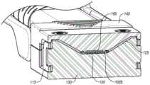
图1A至图1B是作为本发明的第一实施方式的闩锁和屏蔽机构的示例的有源光缆的等距视图;1A-1B are isometric views of an active optical cable as an example of a latching and shielding mechanism of a first embodiment of the present invention;
图2是图1A至图1B中示出的第一实施方式的有源光缆的等距分解图;2 is an isometric exploded view of the active optical cable of the first embodiment shown in FIGS. 1A-1B;
图3A至图3B是以第一实施方式的有源光缆的锁定位置和解锁位置示出的等距视图;3A-3B are isometric views showing the locked and unlocked positions of the active optical cable of the first embodiment;
图4是示出了光如何穿过光收发器模块的透镜传输到第一实施方式的有源光缆的光纤中的截面图;4 is a cross-sectional view showing how light is transmitted through the lens of the optical transceiver module into the optical fiber of the active optical cable of the first embodiment;
图5是示出了第一实施方式的有源光缆的等距视图,其中,顶壳和闩锁未示出;5 is an isometric view showing the active optical cable of the first embodiment, wherein the top shell and latch are not shown;
图6是与第一实施方式结合使用的夹具的等距视图;Figure 6 is an isometric view of a clamp for use in conjunction with the first embodiment;
图7是第一实施方式的有源光缆的截面的俯视图;7 is a plan view of a cross-section of the active optical cable of the first embodiment;
图8是示出了第一实施方式的有源光缆的等距分解图;8 is an isometric exploded view showing the active optical cable of the first embodiment;
图9是示出了第一实施方式的EMI衬垫和EMI粘贴部位置的等距分解图;9 is an isometric exploded view showing the location of the EMI gasket and EMI sticker of the first embodiment;
图10是示出了根据第一实施方式的有源光缆的顶壳的等距截面图,该顶壳容置EMI粘贴部、EMI衬垫和EMI条带;10 is an isometric cross-sectional view showing the top shell of the active optical cable according to the first embodiment, the top shell housing the EMI sticker, the EMI gasket, and the EMI strip;
图11是示出了根据本发明的第一实施方式的有源光缆的顶壳和底壳的狭槽的内部的EMI粘贴部和EMI衬垫的截面图;以及11 is a cross-sectional view showing an EMI sticker and an EMI gasket inside the slots of the top and bottom cases of the active optical cable according to the first embodiment of the present invention; and
图12是示出了根据本发明的第一实施方式的有源光缆的顶壳和底壳的狭槽的内部的EMI粘贴部和EMI衬垫的截面图。12 is a cross-sectional view showing an EMI sticking part and an EMI gasket inside the slots of the top and bottom cases of the active optical cable according to the first embodiment of the present invention.
具体实施方式Detailed ways
将参照附图对本公开的具体实施方式进行描述。在详细说明书、附图和权利要求中描述的示例性实施方式并非意在限制性的。在不脱离本文所提出的主题的精神或范围的情况下,可以采用其他的实施方式并且可以做出其他的修改。如本文总体描述的并如图中所示出的本公开的方面可以以很多种构型进行布置、替代、组合、分离和设计,所有的这些均是本文所明确构思的。Specific embodiments of the present disclosure will be described with reference to the accompanying drawings. The exemplary embodiments described in the detailed description, drawings, and claims are not intended to be limiting. Other embodiments may be utilized, and other modifications may be made, without departing from the spirit or scope of the subject matter presented herein. Aspects of the disclosure as generally described herein and illustrated in the figures may be arranged, substituted, combined, separated, and designed in a wide variety of configurations, all of which are expressly contemplated herein.
本文中公开的各实施方式涉及光学组件。更具体地,一些示例性实施方式涉及一种用于光电模块、线缆锁定机构和线缆保持设计的线缆连接器,该线缆连接器隔离来自光电模块的任何外力并确保套圈与透镜之间的连接是牢固的。本文中描述的各实施方式还提供了多个益处,包括:通过简化组装来简化制造过程的能力以及再加工部件的能力。此外,本文中的各实施方式能够在不修改现有产品的整体尺寸和结构的情况下实施。Various embodiments disclosed herein relate to optical assemblies. More specifically, some exemplary embodiments relate to a cable connector for an optoelectronic module, cable locking mechanism, and cable retention design that isolates any external force from the optoelectronic module and secures the ferrule to the lens The connection between is solid. Embodiments described herein also provide a number of benefits, including the ability to simplify the manufacturing process by simplifying assembly and the ability to rework components. Furthermore, the various embodiments herein can be implemented without modifying the overall size and structure of existing products.
示例性实施方式包括线缆连接器,该线缆连接器可以插入到光电模块中以保持多纤维线缆与光学引擎的接合。在线缆连接器被使用在多通道纤维光缆的两个端部上的实例中,有源光学产品可以设置成具有被牢固地附接至光缆的每个端部的收发器模块。Exemplary embodiments include a cable connector that can be inserted into an optoelectronic module to maintain engagement of the multifiber cable with the optical engine. In instances where cable connectors are used on both ends of a multi-channel fiber optic cable, the active optical product may be provided with a transceiver module securely attached to each end of the fiber optic cable.
尽管在光学网络领域中所使用的光学收发器模块和有源光缆的环境条件下对各实施方式进行了描述,但是应当理解的是,本发明的各实施方式可以在本文所公开的功能可能有用的其他领域和/或操作环境中使用。因此,本发明的范围不应解释为受限于本文所公开的示例性实施方案和操作环境。Although the embodiments are described in the context of optical transceiver modules and active optical cables used in the field of optical networking, it should be understood that embodiments of the present invention may be useful in the functionality disclosed herein used in other domains and/or operating environments. Therefore, the scope of the present invention should not be construed as limited to the exemplary embodiments and operating environments disclosed herein.
现将参照附图对本公开的各实施方式进行说明。Various embodiments of the present disclosure will now be described with reference to the accompanying drawings.
I.现有有源光缆的示例性方面I. Exemplary Aspects of Existing Active Optical Cables
图1A至图1B是QSFP有源光缆产品100的等距视图,该QSFP有源光缆产品100包括具有集成的QSFP收发器模块的QSFP有源光缆190,该集成的QSFP收发器模块是光电模块195的示例。在该示例中,光电模块195是可热插拔的,或者该光电模块195被设计成被插入到较大的电子系统比如主机装置的印刷电路板(PCB)等中。有源光学产品100的把手或提捞机构112使有源光学产品100能够与较大的电子系统连接以及从该较大的电子系统移除,以使光电模块195与较大的电子系统连接和断开连接。然而,有源光学产品100的把手或提捞机构112的一个困难在于,施加至驱动件112的锁定力和断开连接力可能导致有源光缆100被推挤并且导致外力经由包含在有源光缆100中的带状纤维120(图2中示出)传递至有源光学产品100的内部部件。类似地,施加至有源光缆产品100的任何其他的力都可能导致外力传递至有源光学产品100的内部部件。1A-1B are isometric views of a QSFP active
本文中描述的各实施方式提供了一种用于防止外力传递至有源光学产品100的内部部件的机构。如下面关于图3至图4更全面地描述的,本文中所描述的各实施方式的益处在于可以确保光电模块195的透镜与印刷电路板之间的透镜对准。此外,本文中的各实施方式提供了EMI屏蔽以防止来自光电模块195的内部部件的EMI泄漏。Embodiments described herein provide a mechanism for preventing the transmission of external forces to internal components of active
II.有源光缆产品的示例性结构方面II. Exemplary Structural Aspects of Active Optical Cable Products
首先参照图1A、图1B和图2,图1A、图1B和图2示出了根据一个实施方式的有源光缆产品100的示例。如前所述,图1A至图1B是有源光缆产品100的等距视图,而图2是图1A至图1B的有源光缆产品100的等距分解图。Referring first to FIGS. 1A , 1B, and 2, FIGS. 1A, 1B, and 2 illustrate an example of an active
图1A至图1B和图2中描绘的光电模块产品100包括光电模块195。光电模块195的示例可以设计成用于集成电路之间和/或电路板之间的高速(例如,每秒25吉比特(Gbps)或更高)的光学互连。附加地或替代性地,光电模块195可以配置成接收十二、二十四或其他数量的光学通道,这些光学通道中的每个光学通道可以配置成传送数据。The
一旦安装至主机PCB(未示出),光电模块200可以配置成例如在主机装置与网络(未示出)之间传送数据。光电模块200可以将电信号转换成表示电信号的光学信号,光电模块200也可以将光学信号转换成电信号。例如,呈光学信号形式的数据可以沿着有源光缆190从网络传送至光电模块195。光电模块195的部件(该部件的示例在下面描述)可以将光学信号转换成代表光学信号的电信号。然后,电信号可以被传送至主机装置。同样地,主机装置可以将电信号传送至光电模块195。光电模块195可以将电信号转换成代表电信号的光学信号。光学信号可以沿着有源光缆190传送到网络中例如通向另一光电模块195。Once mounted to a host PCB (not shown), the
有源光缆产品100的有源光缆部分190包括MT套圈124、套圈护套122。套圈护套122连接至多个光学带状纤维120,所述多个光学带状纤维120延伸至包括过渡部分103的线缆尾套107,该过渡部分103连接至封围光学带状纤维120的保护管102。Active
如本领域技术人员可以理解的,光学带状纤维120可以在保护管102内和有源光缆部分190的各种其他部件内单独地覆盖有塑料层,有源光缆部分190包括线缆尾套107、MT套圈护套122、MT套圈124。此外,塑料层和保护管102由适合于将要施用有源光缆产品100的环境的材料制成,并且本文中所描述的各实施方式不限于任何特定材料。As can be appreciated by those skilled in the art, the
图2还示出了本实施方式的闩锁机构113。一般而言,闩锁机构113包括驱动件112和从动件109以及一对弹簧160,所述一对弹簧160容纳在包括底壳130和顶壳140的组装体200中。驱动件112和从动件109可以使用包括金属或模制塑料的各种材料以多种方式形成。弹簧160被示出为螺旋弹簧,但是弹簧160也可以用例如扭转弹簧或金属丝弹簧代替。FIG. 2 also shows the
驱动件112构造成通过将驱动件112的突出部111推入从动件109的孔中而在如图3A和图3B所示的锁定位置与解锁位置之间以可旋转的方式附接至从动件109。更具体地,如图3A所示,用户可以在从动件109处于锁定位置时拉动驱动件112的拉环部分108,以经由旋转轴310使连接至驱动件112的从动件109沿箭头示出的方向移动进入解锁位置(图3B示出)。The
从动件109构造成以可滑动的方式附接至组装体200,组装体200包括顶壳140、底壳130、印刷电路板组件(PCBA)150、透镜155、夹具145以及有源光缆部分190。将在下面对组装体200的各个方面进行更全面地描述。
如图2中所公开的,从动件109包括经由横跨部分114连接的一对从动臂104和105。从动臂104和从动臂105包括背对驱动件112的倾斜部117。从动臂104和从动臂105也限定凹部110,所述凹部110构造成与组装体200的底壳130的对应的凸部131以可滑动的方式接合。更具体地,凹部110各自包括矩形窗部116,该矩形窗部116构造成容纳组装体200的底壳130的对应的凸部131。如在图3A和图3B中清楚地示出的,矩形窗部116构造成在线缆插入/移除方向上具有较大的面积,以使组装体200的底壳130的对应的凸部131能够将从动件109以可滑动的方式联接至组装体200。在组装期间,从动件109的从动臂104和从动臂105可以向外弯曲以最初使从动臂104和从动臂105在底壳180的相应的凸部131上滑动,并且然后释放从动臂104和从动臂105使得凸部131分别定位在从动臂104和从动臂105中的每一者的矩形窗部116内。As disclosed in FIG. 2 , the
从动臂104和从动臂105还各自包括凹入的平坦部分118,该凹入的平坦部分118在组装之后容纳在底壳130的平坦的凹入部分132中。从动臂104和从动臂105还包括倾斜的肩部部分119和平坦的颈部部分106,该倾斜的肩部部分119和平坦的颈部部分106形成为与底壳130的倾斜部分135和底壳130的平坦的狭槽134相对应,这有助于施加将从动臂104和从动臂105朝向底壳130的对应的外表面迫压的迫压力。The
如图3A和3B所示,当拉环108沿轴向方向枢转和拉动时,实现了从动件109沿着组装体200的轴向滑动。克服了由图1中公开的弹簧160产生的偏压力。As shown in FIGS. 3A and 3B , when the
尽管示例性闩锁机构113在本文中与示例性主机装置(未示出)和示例性光电模块195结合使用,但是应当理解的是,示例性闩锁机构113可以替代地与其他电子装置和主机设备结合使用。Although the
在将光电模块产品100插入到主机装置的主机笼架中期间,闩锁机构113的驱动件112可以初始处于解锁位置,如图3B所示。用户可以抓住驱动件112并推靠驱动件112以将光电模块产品100插入到主机笼架中。注意的是,在将光电模块产品100插入到主机笼架中的期间,从动臂104和从动臂105的倾斜部117、凹部110、凹入的平坦部分118、倾斜的肩部部分119和平坦的颈部部分106定位和定向成避免与主机笼架的表面接合。During insertion of the
一旦光电模块产品100已经完全插入到主机笼架中,主机笼架的板簧(未示出)通常朝向从动臂104和从动臂105中的每一者的凹入的平坦部分118向内并向前弯曲。此外,一旦处于完全插入位置,光电模块产品100的PCBA150电连接至主机连接器,顶壳140上的凹槽141的端部用作硬止动件,以防止光电模块产品100进一步地插入到主机笼架中。可以使用闩锁机构113来实现保持光电模块产品100的该完全插入位置。Once the
一旦光电模块产品100被完全插入到主机笼架中并进入锁定位置,示例性闩锁机构113将光电模块产品100固定在主机笼架内并抵接主机连接器。光电模块产品100抵接主机连接器实现了相对于主机连接器的严格的公差和精确的对准,这产生了光电模块产品100与主机装置之间的精确的电连接。Once the
现在回到图2,组装体200包括底壳130和顶壳140,底壳130和顶壳140通过一对螺钉170或其他联接装置联接在一起,组装体200容纳PCBA150,其中,在PCBA150上安装有透镜155。如上面简要论述的,使用上述闩锁机构113的一个困难在于,当驱动件112被枢转和拉动时,可能会导致有源光缆部分190被推挤,这又导致带状纤维120将力传递到组装体200的内部,在该组装体200的内部施加至带的力可以被传递至套圈124并且干涉介于套圈123与安装至PCBA150的透镜155之间的连接。本文中所描述的各实施方式通过使用夹具145以及线缆尾套107上的适配器410(在下面相对于图5更全面地描述)来防止这种力的传递,夹具145形成为基本上围绕透镜155和套圈124并且确保透镜155与套圈124之间的连接。Returning now to FIG. 2, the
图4示出了光被从安装在PCBA150上的透镜155传输到带状纤维120中的过程。如图4所示,结合在PCBA150的表面上的有源芯片450传输光,该光由透镜155(在该示例中为直角联接透镜)的45度镜面反射并具有沿着光路400朝向容纳在套圈124中的带状纤维120传输的全内反射。如本领域技术人员可以理解的,透镜155与套圈124之间的对准和连接是必要的以确保光学信号沿着带状纤维120被适当地传输。FIG. 4 shows the process of light being transmitted from the
为了确保这种连接,图5示出了夹具145的使用。在图5中示出的视图中,已经移除了顶壳140以更清楚地显示夹具145以及线缆尾套107的适配器410的放置。图6是夹具145的单独的等距视图以清楚地示出夹具145的各个方面。To ensure this connection, Figure 5 shows the use of a
如图5所示,夹具145构造成基本上围绕套圈124和透镜155以保持套圈124与透镜155的适当连接。转至图6,夹具145呈大致矩形形状并且前侧部635具有狭槽625,狭槽625形成在前侧部635中并成形为配装在套圈护套122上。在该实施方式中,狭槽625包括弯曲的拐角627,尽管可以省略该弯曲的拐角627。前侧部635的内侧表面具有形成在该内侧表面中的柱605,所述柱605形成为与套圈孔126(如图2所示)配合,所述套圈孔126形成在套圈124的表面中,该套圈124的表面在组装期间当夹具145附接至有源光缆产品100时面向套圈护套122。As shown in FIG. 5 , clamp 145 is configured to substantially surround
如可以理解的,夹具145可以由各种材料形成,包括但不限于模制塑料。As can be appreciated, the
该示例的夹具145的后表面660包括三个弯曲表面615、620和621。更具体地,后表面660包括从夹具145的内侧向外凸出的凸形表面620和凸形表面621以及形成在凸形表面620与凸形表面621之间的凹形表面615。凹形表面615以及形成在夹具145的侧表面640和侧表面650中的每一者中的突出的倾斜部610锁定或夹持在透镜155上,如图5和7所示。更具体地,凹形表面615锁定到透镜155的与套圈124连接至透镜155的表面相反的表面上,并且突出的倾斜部610锁定到凹部156(在图2中示出)上,该凹部156形成在透镜155的对应的侧表面中。凹形表面615形成为当围绕套圈124和透镜155组装时能够变形,并且一旦组装,该凹形表面615施加将套圈124紧紧地保持至透镜155的压缩力以确保套圈124与透镜之间的连接,并且避免由带状纤维120施加的拉伸、扭曲或弯曲运动而引起的施加在接合面上的任何力。The
在一些实施方式中,从透镜155的内部延伸的金属销705(在图2中示出)也可以延伸到套圈124中以确保透镜155与套圈124之间的适当连接。In some embodiments, metal pins 705 (shown in FIG. 2 ) extending from the interior of the
图5和图8还示出了本文中所描述的各实施方式的另一方面,该方面提供了线缆尾套107与组装体200之间的更牢固的连接,组装体200包括底壳130和顶壳140。更具体地,如图8所示,线缆尾套107包括适配器410,该适配器410包括一对倾斜的插脚800和805,所述一对倾斜的插脚800和805构造成容纳在形成于底壳130的前表面中的对应的狭槽810和狭槽820中。如图8所示,当有源光缆产品100被组装时,适配器410的倾斜的插脚800和倾斜的插脚805分别从侧面进入狭槽810和狭槽820。如本领域技术人员可以理解的,实施方式的该方面使得带状纤维120和电缆101被锁定在底壳130与顶壳140之间的位置中。中间护套405形成在带状纤维120上并作为线缆尾套107的一部分,并且当组装时,中间护套405容纳在底壳130的对应的容纳部分840中。FIGS. 5 and 8 also illustrate another aspect of the various embodiments described herein that provide a stronger connection between the
将带状纤维120通过使用适配器410和夹具145锁定在线缆尾套107与套圈护套122之间,带状纤维120被固定并且施加至线缆101的任何外力被转移到有源光缆产品100的内部从而破坏套圈124与透镜155之间的连接的可能性如果没有完全消除的话则被减小。By locking the
此外,在有源光缆产品100的部件的维护、再加工或测试变得必要的情况下,夹具145、闩锁机构113和适配器410都能够分离并容易地拆卸。因此,实施方式提供了具有牢固的连接的能力,同时提供了可以在必要时拆卸的解决方案。Additionally, the
图9至图12示出了实施方式的另一方面,该方面包括防止电磁波从有源光缆产品100的内部泄漏的能力。更具体地,实施方式包括电磁干扰(EMI)衬垫165和EMI粘贴部125,如图9所示。也可以使用EMI条带900,如图12所示。FIGS. 9-12 illustrate another aspect of the embodiment that includes the ability to prevent electromagnetic waves from leaking from the interior of the active
更具体地,如图9所示,图9示出了组装的有源光缆产品100,其中,移除了顶壳130以更清楚地示出内部部件,本文中所描述的各实施方式可以包括EMI衬垫165,该EMI衬垫165在底壳130的平坦的内部部分910(在图5中更清楚地示出)处定位在带状纤维120上。如图5和图9所示,EMI粘贴部125沿着底壳130的侧壁920和内部肋状件915形成以防止EMI从有源光缆产品100的内部泄漏。More specifically, as shown in FIG. 9, which shows the assembled active
图10示出了顶壳130的内部表面1000以说明顶壳130的压缩特征,该压缩特征在顶壳130连接至底壳140时压缩EMI衬垫165、EMI粘贴部125和EMI条带900。内部表面1000包括狭槽1015和肋状件1005,狭槽1015形成在每个侧部中并容纳EMI粘贴部125,肋状件1005压缩EMI衬垫165和EMI条带900。内部表面1000还包括螺钉容纳部1020,所述螺钉容纳部1020在顶壳140和底壳130组装在一起时朝向图5中示出的底壳130的接收部930导引螺钉170。FIG. 10 shows the
内部表面1000还包括狭槽1010,该狭槽1010形成为与底壳130的有助于将线缆尾套107的适配器410锁定到位的狭槽810和狭槽820相对应。The
图11和图12是示出了EMI衬垫165、EMI粘贴部125和EMI条带900的截面图,EMI衬垫165、EMI粘贴部125和EMI衬垫165形成在顶壳140与底壳130之间以基本上围绕并覆盖带状纤维120从而进一步固定带状纤维120并防止在有源光缆产品100的内部产生的电磁波泄漏至有源光缆产品100的外部。FIGS. 11 and 12 are cross-sectional views showing the
如本领域技术人员可以理解的,通过防止EMI泄漏,本文中的各实施方式通过包括EMI提供了更可靠的有源光缆产品100,同时提供了简单的机械结构,该简单的机械结构对有源光缆190的带状纤维120进行固定以在套圈124与光电模块195的透镜155之间提供更可靠的连接,并且该简单的机械结构使用闩锁机构113,该闩锁机构113提供了改进的缩回、减小了闩锁机构113与组装体200之间的摩擦,并且降低了有源光缆产品100的总体高度。如上面清楚地说明的,本文中所描述的各实施方式提供了现有技术目前没有教导或建议的各种益处。As can be appreciated by those skilled in the art, by preventing EMI leakage, the embodiments herein provide a more reliable active
所描述的各实施方式在所有方面被认为是仅作为示例性的而非限制性的。因此,本发明的范围由所附权利要求而非前述描述来表示。在权利要求的等同意义和范围内的所有变化均被包含在权利要求书的范围内。The described embodiments are considered in all respects to be illustrative only and not restrictive. Accordingly, the scope of the invention is indicated by the appended claims rather than the foregoing description. All changes that come within the equivalency and range of the claims are intended to be embraced within the scope of the claims.
Claims (20)
Translated fromChineseApplications Claiming Priority (3)
| Application Number | Priority Date | Filing Date | Title |
|---|---|---|---|
| US14/643,933US20160266340A1 (en) | 2015-03-10 | 2015-03-10 | Latching and emi shielding mechanism for an optical module |
| US14/643,933 | 2015-03-10 | ||
| PCT/US2016/021860WO2016145246A1 (en) | 2015-03-10 | 2016-03-10 | Latching and emi shielding mechanism for an optical module |
Publications (2)
| Publication Number | Publication Date |
|---|---|
| CN107567593A CN107567593A (en) | 2018-01-09 |
| CN107567593Btrue CN107567593B (en) | 2020-06-05 |
Family
ID=55637466
Family Applications (1)
| Application Number | Title | Priority Date | Filing Date |
|---|---|---|---|
| CN201680026778.7AExpired - Fee RelatedCN107567593B (en) | 2015-03-10 | 2016-03-10 | Latch and EMI shielding mechanism for optical modules |
Country Status (6)
| Country | Link |
|---|---|
| US (1) | US20160266340A1 (en) |
| EP (1) | EP3268788A1 (en) |
| JP (2) | JP2018508046A (en) |
| CN (1) | CN107567593B (en) |
| CA (1) | CA2979395A1 (en) |
| WO (1) | WO2016145246A1 (en) |
Families Citing this family (32)
| Publication number | Priority date | Publication date | Assignee | Title |
|---|---|---|---|---|
| JP2016224346A (en)* | 2015-06-02 | 2016-12-28 | 富士通コンポーネント株式会社 | Optical connector |
| WO2017188989A1 (en)* | 2016-04-29 | 2017-11-02 | Hewlett Packard Enterprise Development Lp | Cage assembly for optical modules |
| US10591689B2 (en)* | 2017-02-06 | 2020-03-17 | Oracle International Corporation | Reflow-compatible optical I/O assembly adapter |
| JP2018169490A (en)* | 2017-03-30 | 2018-11-01 | 富士通コンポーネント株式会社 | Extraction component and optical module |
| US10797797B2 (en)* | 2017-03-31 | 2020-10-06 | Nexans | Fiber optic extender |
| US10440799B2 (en)* | 2017-04-06 | 2019-10-08 | Hisense Broadband Multimedia Technologies Co., Ltd. | Optical module |
| JP2019028410A (en)* | 2017-08-04 | 2019-02-21 | 富士通コンポーネント株式会社 | Optical connector |
| WO2019100379A1 (en)* | 2017-11-27 | 2019-05-31 | 昂纳信息技术(深圳)有限公司 | Optical fiber plugging structure and system |
| KR102206368B1 (en)* | 2017-12-05 | 2021-01-22 | 주식회사 라이팩 | Connector Plug and Active Optical Cable Assembly Using the Same |
| CN108051893B (en)* | 2017-12-11 | 2020-01-07 | 青岛海信宽带多媒体技术有限公司 | Optical module |
| US10809474B2 (en)* | 2017-12-18 | 2020-10-20 | Ii-Vi Delaware, Inc. | Small footprint parallel optics transceivers |
| CN108037568B (en)* | 2017-12-22 | 2025-03-14 | 昂纳科技(深圳)集团股份有限公司 | An optical module |
| USD887991S1 (en)* | 2018-03-06 | 2020-06-23 | Adolite Inc. | Optical module |
| US10641977B2 (en)* | 2018-04-13 | 2020-05-05 | Finisar Corporation | Optical subassembly with detachably-coupling holder |
| US10955628B2 (en)* | 2018-07-31 | 2021-03-23 | Lumentum Operations Llc | Latching for a transceiver module |
| TW202022423A (en)* | 2018-12-06 | 2020-06-16 | 美商真光公司 | Pluggable optical transceiver module |
| JP7347146B2 (en)* | 2019-11-15 | 2023-09-20 | 富士通オプティカルコンポーネンツ株式会社 | optical module |
| JP7518491B2 (en)* | 2019-12-25 | 2024-07-18 | 株式会社ヨコオ | Optical connector mechanism and optical connector |
| WO2021134657A1 (en)* | 2019-12-31 | 2021-07-08 | 华为技术有限公司 | Optical module unlocking device, optical module, and optical communication device |
| WO2021174921A1 (en)* | 2020-03-05 | 2021-09-10 | 青岛海信宽带多媒体技术有限公司 | Optical module |
| US12078848B2 (en) | 2020-03-05 | 2024-09-03 | Hisense Broadband Multimedia Technologies Co., Ltd. | Optical module |
| JP2023527519A (en)* | 2020-05-20 | 2023-06-29 | コムスコープ テクノロジーズ リミティド ライアビリティ カンパニー | active optical cable assembly |
| WO2021232716A1 (en)* | 2020-05-22 | 2021-11-25 | 青岛海信宽带多媒体技术有限公司 | Optical module |
| CN212647093U (en)* | 2020-08-28 | 2021-03-02 | 青岛海信宽带多媒体技术有限公司 | Optical module |
| US11320601B2 (en)* | 2020-09-24 | 2022-05-03 | Applied Optoelectronics, Inc. | Locking arrangements for pluggable optical subassembly modules |
| JP7596728B2 (en) | 2020-11-12 | 2024-12-10 | 住友電気工業株式会社 | Optical Transceiver |
| US11619789B2 (en)* | 2021-07-28 | 2023-04-04 | Quanta Computer Inc. | Dual connector carrier with simultaneous locking mechanism |
| TWI795057B (en)* | 2021-11-02 | 2023-03-01 | 佳必琪國際股份有限公司 | Cable connector |
| CN114935798B (en)* | 2022-05-11 | 2024-07-05 | 翔光光通讯器材(昆山)有限公司 | Optical module |
| CN114994839B (en)* | 2022-06-24 | 2023-08-08 | 青岛海信宽带多媒体技术有限公司 | Optical module |
| CN114879324B (en)* | 2022-06-24 | 2023-08-08 | 青岛海信宽带多媒体技术有限公司 | Optical module |
| WO2025000714A1 (en)* | 2023-06-30 | 2025-01-02 | 青岛海信宽带多媒体技术有限公司 | Optical module |
Family Cites Families (20)
| Publication number | Priority date | Publication date | Assignee | Title |
|---|---|---|---|---|
| JPH09130076A (en)* | 1995-10-26 | 1997-05-16 | Kokusai Electric Co Ltd | Electromagnetic shield device |
| US7047054B2 (en)* | 1999-03-12 | 2006-05-16 | Cas Medical Systems, Inc. | Laser diode optical transducer assembly for non-invasive spectrophotometric blood oxygenation monitoring |
| TW453862B (en)* | 1999-08-30 | 2001-09-11 | Cas Medical Systems Inc | Near infrared spectrophotometric monitoring assembly for non-invasive monitoring of blood oxygenation levels in a subjects's body |
| US6851867B2 (en)* | 2001-04-14 | 2005-02-08 | Jds Uniphase Corporation | Cam-follower release mechanism for fiber optic modules with side delatching mechanisms |
| US6916123B2 (en)* | 2002-09-10 | 2005-07-12 | Jds Uniphase Corporation | Unlatching mechanism for an optical transceiver |
| JP2004246279A (en)* | 2003-02-17 | 2004-09-02 | Seiko Epson Corp | Optical module and manufacturing method thereof, optical communication device, opto-electric hybrid integrated circuit, circuit board, electronic equipment |
| US7090523B2 (en)* | 2004-01-06 | 2006-08-15 | Tyco Electronics Corporation | Release mechanism for transceiver module assembly |
| US7578623B2 (en)* | 2006-08-21 | 2009-08-25 | Intel Corporation | Aligning lens carriers and ferrules with alignment frames |
| US7371014B2 (en)* | 2006-08-21 | 2008-05-13 | Intel Corporation | Monolithic active optical cable assembly for data device applications and various connector types |
| JP5973745B2 (en)* | 2011-03-31 | 2016-08-23 | 住友電気工業株式会社 | Optical transceiver |
| CN102859410B (en)* | 2009-11-03 | 2015-07-08 | 3M创新有限公司 | Fiber optic device and method of manufacturing fiber optic device |
| JP2011247952A (en)* | 2010-05-24 | 2011-12-08 | Furukawa Electric Co Ltd:The | Optical module |
| US8297856B2 (en)* | 2010-12-13 | 2012-10-30 | Sae Magnetics (H.K.) Ltd. | Electro-optical module and multi-functional latch member therefor |
| US8717770B2 (en)* | 2011-04-28 | 2014-05-06 | Finisar Corporation | Latching mechanisms for pluggable electronic devices |
| US8588572B2 (en)* | 2011-11-28 | 2013-11-19 | Avago Technologies General Ip (Singapore) Pte. Ltd. | Electromagnetic interference (EMI) waveguide device for use in a parallel optical communications module, and a method |
| US9417408B2 (en)* | 2012-03-02 | 2016-08-16 | Tyco Electronics Corporation | Modularized interposer |
| TWI461775B (en)* | 2012-09-26 | 2014-11-21 | Delta Electronics Inc | Optical module and optical coupling method using the same |
| US8790022B2 (en)* | 2012-12-18 | 2014-07-29 | Avago Technologies General Ip (Singapore) Pte. Ltd. | Pluggable data communication module with slider-crank delatch mechanism |
| JP6459615B2 (en)* | 2015-02-24 | 2019-01-30 | 住友電気工業株式会社 | Optical data link |
| US20160377800A1 (en)* | 2015-06-23 | 2016-12-29 | Panasonic Liquid Crystal Display Co., Ltd. | Backlight system for liquid crystal display devices |
- 2015
- 2015-03-10USUS14/643,933patent/US20160266340A1/ennot_activeAbandoned
- 2016
- 2016-03-10CACA2979395Apatent/CA2979395A1/ennot_activeAbandoned
- 2016-03-10CNCN201680026778.7Apatent/CN107567593B/ennot_activeExpired - Fee Related
- 2016-03-10JPJP2017547413Apatent/JP2018508046A/enactivePending
- 2016-03-10WOPCT/US2016/021860patent/WO2016145246A1/ennot_activeCeased
- 2016-03-10EPEP16712140.9Apatent/EP3268788A1/ennot_activeWithdrawn
- 2019
- 2019-07-10JPJP2019128202Apatent/JP2020003797A/ennot_activeWithdrawn
Also Published As
| Publication number | Publication date |
|---|---|
| JP2018508046A (en) | 2018-03-22 |
| EP3268788A1 (en) | 2018-01-17 |
| JP2020003797A (en) | 2020-01-09 |
| CA2979395A1 (en) | 2016-09-15 |
| CN107567593A (en) | 2018-01-09 |
| US20160266340A1 (en) | 2016-09-15 |
| WO2016145246A1 (en) | 2016-09-15 |
Similar Documents
| Publication | Publication Date | Title |
|---|---|---|
| CN107567593B (en) | Latch and EMI shielding mechanism for optical modules | |
| US10466427B2 (en) | Optical module with integrated lens | |
| JP4093862B2 (en) | Optical fiber module latch release mechanism | |
| US10976506B2 (en) | Optical transceiver | |
| US10156689B2 (en) | Latch for communication module | |
| EP2548062B1 (en) | Fiber optic interface devices for electronic devices | |
| EP3682277B1 (en) | Fiber optic connector with boot-integrated release | |
| CN107580687B (en) | Cable connector retention design | |
| US10379295B2 (en) | Connector assemblies for hybrid fiber/wire connections | |
| US20080056647A1 (en) | Active modular optoelectronic components | |
| US11754789B2 (en) | Fiber optic connector with unitary housing and fiber optic connector assembly | |
| CN106483610A (en) | Optical transceiver module and optical fiber cable module | |
| CN101494337A (en) | Connector assembly having a slider element | |
| US20190187392A1 (en) | Small footprint parallel optics transceivers | |
| CN114779414B (en) | Optical module | |
| US12092884B2 (en) | Optical transceiver including connector coupler with elastic holding arm for holding connector | |
| JP7518491B2 (en) | Optical connector mechanism and optical connector | |
| TWM628071U (en) | Optical transceiver and optical switch | |
| WO2025000714A1 (en) | Optical module |
Legal Events
| Date | Code | Title | Description |
|---|---|---|---|
| PB01 | Publication | ||
| PB01 | Publication | ||
| SE01 | Entry into force of request for substantive examination | ||
| SE01 | Entry into force of request for substantive examination | ||
| GR01 | Patent grant | ||
| GR01 | Patent grant | ||
| CF01 | Termination of patent right due to non-payment of annual fee | ||
| CF01 | Termination of patent right due to non-payment of annual fee | Granted publication date:20200605 Termination date:20210310 |