CN107561719B - Autostereoscopic 3D Display - Google Patents
Autostereoscopic 3D DisplayDownload PDFInfo
- Publication number
- CN107561719B CN107561719BCN201710521871.1ACN201710521871ACN107561719BCN 107561719 BCN107561719 BCN 107561719BCN 201710521871 ACN201710521871 ACN 201710521871ACN 107561719 BCN107561719 BCN 107561719B
- Authority
- CN
- China
- Prior art keywords
- lower electrode
- electrodes
- barrier
- display
- electrode
- Prior art date
- Legal status (The legal status is an assumption and is not a legal conclusion. Google has not performed a legal analysis and makes no representation as to the accuracy of the status listed.)
- Active
Links
Images


Classifications
- H—ELECTRICITY
- H04—ELECTRIC COMMUNICATION TECHNIQUE
- H04N—PICTORIAL COMMUNICATION, e.g. TELEVISION
- H04N13/00—Stereoscopic video systems; Multi-view video systems; Details thereof
- H04N13/30—Image reproducers
- H04N13/302—Image reproducers for viewing without the aid of special glasses, i.e. using autostereoscopic displays
- H04N13/305—Image reproducers for viewing without the aid of special glasses, i.e. using autostereoscopic displays using lenticular lenses, e.g. arrangements of cylindrical lenses
- G—PHYSICS
- G02—OPTICS
- G02B—OPTICAL ELEMENTS, SYSTEMS OR APPARATUS
- G02B30/00—Optical systems or apparatus for producing three-dimensional [3D] effects, e.g. stereoscopic images
- G02B30/20—Optical systems or apparatus for producing three-dimensional [3D] effects, e.g. stereoscopic images by providing first and second parallax images to an observer's left and right eyes
- G02B30/26—Optical systems or apparatus for producing three-dimensional [3D] effects, e.g. stereoscopic images by providing first and second parallax images to an observer's left and right eyes of the autostereoscopic type
- G02B30/27—Optical systems or apparatus for producing three-dimensional [3D] effects, e.g. stereoscopic images by providing first and second parallax images to an observer's left and right eyes of the autostereoscopic type involving lenticular arrays
- G—PHYSICS
- G02—OPTICS
- G02B—OPTICAL ELEMENTS, SYSTEMS OR APPARATUS
- G02B30/00—Optical systems or apparatus for producing three-dimensional [3D] effects, e.g. stereoscopic images
- G02B30/20—Optical systems or apparatus for producing three-dimensional [3D] effects, e.g. stereoscopic images by providing first and second parallax images to an observer's left and right eyes
- G02B30/26—Optical systems or apparatus for producing three-dimensional [3D] effects, e.g. stereoscopic images by providing first and second parallax images to an observer's left and right eyes of the autostereoscopic type
- G02B30/30—Optical systems or apparatus for producing three-dimensional [3D] effects, e.g. stereoscopic images by providing first and second parallax images to an observer's left and right eyes of the autostereoscopic type involving parallax barriers
- G02B30/31—Optical systems or apparatus for producing three-dimensional [3D] effects, e.g. stereoscopic images by providing first and second parallax images to an observer's left and right eyes of the autostereoscopic type involving parallax barriers involving active parallax barriers
- G—PHYSICS
- G02—OPTICS
- G02F—OPTICAL DEVICES OR ARRANGEMENTS FOR THE CONTROL OF LIGHT BY MODIFICATION OF THE OPTICAL PROPERTIES OF THE MEDIA OF THE ELEMENTS INVOLVED THEREIN; NON-LINEAR OPTICS; FREQUENCY-CHANGING OF LIGHT; OPTICAL LOGIC ELEMENTS; OPTICAL ANALOGUE/DIGITAL CONVERTERS
- G02F1/00—Devices or arrangements for the control of the intensity, colour, phase, polarisation or direction of light arriving from an independent light source, e.g. switching, gating or modulating; Non-linear optics
- G02F1/01—Devices or arrangements for the control of the intensity, colour, phase, polarisation or direction of light arriving from an independent light source, e.g. switching, gating or modulating; Non-linear optics for the control of the intensity, phase, polarisation or colour
- G02F1/13—Devices or arrangements for the control of the intensity, colour, phase, polarisation or direction of light arriving from an independent light source, e.g. switching, gating or modulating; Non-linear optics for the control of the intensity, phase, polarisation or colour based on liquid crystals, e.g. single liquid crystal display cells
- G02F1/133—Constructional arrangements; Operation of liquid crystal cells; Circuit arrangements
- G02F1/1333—Constructional arrangements; Manufacturing methods
- G02F1/1343—Electrodes
- H—ELECTRICITY
- H04—ELECTRIC COMMUNICATION TECHNIQUE
- H04N—PICTORIAL COMMUNICATION, e.g. TELEVISION
- H04N13/00—Stereoscopic video systems; Multi-view video systems; Details thereof
- H04N13/10—Processing, recording or transmission of stereoscopic or multi-view image signals
- H04N13/106—Processing image signals
- H04N13/111—Transformation of image signals corresponding to virtual viewpoints, e.g. spatial image interpolation
- H—ELECTRICITY
- H04—ELECTRIC COMMUNICATION TECHNIQUE
- H04N—PICTORIAL COMMUNICATION, e.g. TELEVISION
- H04N13/00—Stereoscopic video systems; Multi-view video systems; Details thereof
- H04N13/10—Processing, recording or transmission of stereoscopic or multi-view image signals
- H04N13/106—Processing image signals
- H04N13/128—Adjusting depth or disparity
- H—ELECTRICITY
- H04—ELECTRIC COMMUNICATION TECHNIQUE
- H04N—PICTORIAL COMMUNICATION, e.g. TELEVISION
- H04N13/00—Stereoscopic video systems; Multi-view video systems; Details thereof
- H04N13/30—Image reproducers
- H04N13/302—Image reproducers for viewing without the aid of special glasses, i.e. using autostereoscopic displays
- H04N13/31—Image reproducers for viewing without the aid of special glasses, i.e. using autostereoscopic displays using parallax barriers
- H04N13/315—Image reproducers for viewing without the aid of special glasses, i.e. using autostereoscopic displays using parallax barriers the parallax barriers being time-variant
- H—ELECTRICITY
- H04—ELECTRIC COMMUNICATION TECHNIQUE
- H04N—PICTORIAL COMMUNICATION, e.g. TELEVISION
- H04N13/00—Stereoscopic video systems; Multi-view video systems; Details thereof
- H04N2013/0074—Stereoscopic image analysis
- H04N2013/0081—Depth or disparity estimation from stereoscopic image signals
Landscapes
- Physics & Mathematics (AREA)
- Engineering & Computer Science (AREA)
- Multimedia (AREA)
- Signal Processing (AREA)
- General Physics & Mathematics (AREA)
- Optics & Photonics (AREA)
- Nonlinear Science (AREA)
- Mathematical Physics (AREA)
- Chemical & Material Sciences (AREA)
- Crystallography & Structural Chemistry (AREA)
Abstract
Description
Translated fromChinese技术领域technical field
本公开涉及使用切换屏障(switchable barrier)的自动立体三维(或3D)显示器。The present disclosure relates to autostereoscopic three-dimensional (or 3D) displays using switchable barriers.
背景技术Background technique
由于立体图像显示技术的发展,立体图像重现技术被应用于诸如电视或监视器这样的显示装置,使得任何人都能够在任何地方欣赏立体图像。立体图像显示器可以被定义为用于人为重现3D图像的系统。Due to the development of stereoscopic image display technology, the stereoscopic image reproduction technology is applied to display devices such as televisions or monitors, enabling anyone to enjoy stereoscopic images anywhere. A stereoscopic image display can be defined as a system for artificially reproducing 3D images.
人从视觉上感到立体感的原因是因为双眼视差,双眼视差是由眼睛在水平方向上分隔开65mm的事实造成的。当人的眼睛观察事物时,因为双眼视差,两只眼中的每一只分别看到从略微不同角度观察到的不同图像。当这两个图像通过视网膜被发送到大脑时,大脑能够通过精确组合这两个图像来识别立体图像。The reason why people visually perceive three-dimensionality is because of binocular parallax, which is caused by the fact that the eyes are separated by 65mm in the horizontal direction. When human eyes observe things, each of the two eyes sees a different image viewed from slightly different angles because of binocular parallax. When the two images are sent to the brain through the retina, the brain is able to recognize the stereoscopic image by precisely combining the two images.
自动立体3D显示器通过根据双眼视差的机制在二维显示器中显示左眼图像和右眼图像二者并且将它们分别发送到左眼和右眼的设计来产生虚拟立体效果。作为用于实现双眼视差的方法,已经开发出眼镜型(或眼镜式)显示器和非眼镜型(或非眼镜式)显示器。Autostereoscopic 3D displays produce virtual stereoscopic effects by displaying both left-eye and right-eye images in a two-dimensional display according to a mechanism of binocular parallax and sending them to the left and right eyes, respectively. As methods for realizing binocular parallax, glasses-type (or glasses-type) displays and non-glasses-type (or non-glasses-type) displays have been developed.
眼镜型显示器被划分成时分系统和空分系统。在时分系统中,利用时间延迟来依次显示左眼图像和右眼图像,并且使用快门眼镜或偏振眼镜来提供立体图像。在空分系统中,同时显示左眼图像和右眼图像,但是分别向左眼图像和右眼图像中的每一个提供不同的偏振光。使用偏振眼镜或快门眼镜来提供立体图像。The glasses-type display is divided into a time division system and a space division system. In the time division system, the left eye image and the right eye image are sequentially displayed with a time delay, and shutter glasses or polarized glasses are used to provide a stereoscopic image. In a space-division system, the left-eye image and the right-eye image are displayed simultaneously, but each of the left-eye and right-eye images is provided with different polarized light, respectively. Use polarized glasses or shutter glasses to provide stereoscopic images.
在非眼镜型显示器(或“自动立体3D显示器”)中,同时显示左眼图像和右眼图像,并且这两个图像的光学轴彼此分隔开。这些图像被分别提供给左眼和右眼。非眼镜型显示器可以被划分成视差屏障系统、双凸透镜系统和集成拍摄系统。在视差屏障系统中,在显示器前部上设置垂直栅格状空隙,以将左眼图像和右眼图像分开。在双凸透镜系统中,将连续排列有多个半柱面镜的透镜膜附接到显示器的前表面,以提供左眼图像和右眼图像。集成拍摄系统使用蜻蜓眼状透镜板来将左眼图像和右眼图像分开。In a glasses-free display (or "autostereoscopic 3D display"), a left-eye image and a right-eye image are displayed simultaneously, with the optical axes of these two images spaced apart from each other. These images are provided to the left and right eyes, respectively. Non-glasses type displays can be classified into parallax barrier systems, lenticular lens systems, and integrated photographing systems. In a parallax barrier system, a vertical grid-like void is provided on the front of the display to separate left-eye and right-eye images. In a lenticular lens system, a lens film with a plurality of semi-cylindrical mirrors arranged in series is attached to the front surface of the display to provide left-eye and right-eye images. The integrated capture system uses a dragonfly-eye lens plate to separate the left-eye image from the right-eye image.
近来,已经开发出具有使用液晶单元的视差屏障或双凸透镜的3D单元。根据相关技术的视差屏障或双凸透镜是固定光学透镜膜型的,其中,当观察者正在移动或者显示器改变其位置时,欣赏到正常的立体图像并不困难。相反,对于液晶3D单元,通过用电方式控制液晶层,切换屏障或切换透镜表现为取代了视差屏障或双凸透镜。另外,如有需要,可以将切换屏障或切换透镜移向左侧或右侧,使得观察者即便正在移动也能够一直正常地欣赏到立体图像。Recently, 3D cells with parallax barriers or lenticular lenses using liquid crystal cells have been developed. The parallax barrier or lenticular lens according to the related art is of a fixed optical lens film type in which it is not difficult to appreciate a normal stereoscopic image when the observer is moving or the display changes its position. In contrast, for liquid crystal 3D cells, by electrically controlling the liquid crystal layer, the switching barrier or switching lens appears to replace the parallax barrier or lenticular lens. In addition, if necessary, the switching barrier or the switching lens can be moved to the left or right, so that the observer can always enjoy the stereoscopic image normally even if they are moving.
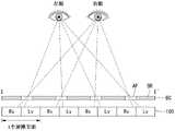
图1是例示根据相关技术的自动立体3D显示器的示意图。参照图1,自动立体3D显示器包括显示面板100、显示面板驱动器130、3D单元驱动器210、定时控制器101等。FIG. 1 is a schematic diagram illustrating an autostereoscopic 3D display according to the related art. 1, the autostereoscopic 3D display includes a
显示面板100可以是诸如液晶显示器(或“LCD”)、场发射显示器(或“FED”)、等离子体显示面板(或“PDP”)、有机发光二极管显示器(或OLED)等这样的平板显示器。显示面板100可以包括彼此交叉的多条数据线105和多条选通线(或扫描线)106。在限定数据线105和选通线106的交叉结构的矩形区域中的每一个处,分别布置像素PXL。每个像素可以包括多个子像素,每个子像素具有唯一颜色。显示面板100在2D模式下呈现2D图像,而在3D模式下呈现左眼图像和右眼图像。The
显示面板驱动器130可以包括数据驱动电路102和选通驱动电路103。数据驱动电路102向数据线105供应2D图像数据电压或3D图像数据电压。选通驱动电路103向选通线106依次供应选通脉冲(或扫描脉冲)。在3D模式下,显示面板驱动器130可以通过使用空分方法将左眼图像数据和右眼图像数据分开来将它们供应到显示面板100的像素。The
数据驱动电路102可以将从定时控制器101接收的数字视频数据转换成模拟伽马电压,然后将数据电压供应到数据线105。选通驱动电路103可以通过定时控制器101向选通线106供应选通脉冲,其中,选通脉冲是用于向数据线105供应数据电压的与数据电压同步的信号。选通脉冲被依次供应到选通线106。The
定时控制器101将来自主机系统110的2D/3D输入图像的数字视频数据RGB供应到数据驱动电路102。利用数字视频数据RGB,定时控制器101接收来自主机系统110的诸如垂直同步信号、水平同步信号、数据使能信号和主时钟这样的定时信号。使用从主机系统110接收的定时信号,定时控制器101控制显示面板驱动器130和3D单元驱动器210各自的操作定时,并且生成用于将驱动器的操作定时同步的定时控制信号DDC、GDC和3DC。The
可以在主机系统110和定时控制器101之间设置3D数据格式器120。在3D模式下,3D数据格式器120将从主机系统110接收的3D图像的左眼图像和右眼图像重新排列成预定数据格式,并且将左眼图像和右眼图像发送到定时控制器101。The
主机系统110可以是电视机、机顶盒、导航系统、DVD播放器、蓝光播放器、个人计算机、家庭影院系统或智能电话系统中的任一种。使用定标器,主机系统110可以将2D/3D输入图像的数字视频数据转换成对于显示面板100的分辨率而言正确的格式,然后将格式转换后的视频数据与定时信号一起发送到定时控制器101。The
主机系统110在2D模式下向定时控制器101供应2D图像,而在3D模式下向3D数据格式器120供应2D图像或3D图像数据。响应于经由用户接口112的用户数据,主机系统110将所有信号发送到定时控制器101,以将非眼镜型立体显示器的操作模式选择为2D模式或3D模式。用户接口112可以配置有键区、键盘、鼠标、屏幕显示(或“OSD”)、远程控制器、图形用户接口、触摸用户接口、语音识别用户接口、3D用户接口等。The
3D单元200可以包括视差屏障。3D单元200可以设置在显示面板100的前面或后面或者内置于显示面板100中,使得它能够划分3D图像的左图像和右图像的光。3D单元驱动器210通过定时控制器101来进行与供应到显示面板100的像素的数据同步的驱动操作。The
对于视差屏障型自动立体3D显示器,将视差屏障膜附接在显示面板100上。将具有固定视差屏障图案的膜附接在显示面板100的表面上。因此,为了使观察者正常地欣赏立体图像,他/她应该位于最佳位置。例如,当观察者位于最佳距离处时,如果没有位于最佳角度范围内,则他/她不能欣赏正常立体图像。另外,当视差屏障图案的大小和节距固定时,根据显示面板100的像素大小和分辨率,显示面板100需要具有独特设计的视差屏障图案。For a parallax barrier type autostereoscopic 3D display, a parallax barrier film is attached on the
发明内容SUMMARY OF THE INVENTION
为了克服上述缺点,本公开的目的是提供使用液晶面板的具有切换屏障的自动立体3D显示器。本公开的另一个目的是提供具有不受显示面板结构影响的切换屏障的自动立体3D显示器,在切换屏障中限定了空隙区域(aperture area)。本公开的又一个目的是提供具有优异立体图像的自动立体3D显示器,其中,通过将电极的三个层叠堆并且防止电极之间的电短路来增加代表切换屏障的电极的数目。In order to overcome the above disadvantages, an object of the present disclosure is to provide an autostereoscopic 3D display with a switching barrier using a liquid crystal panel. Another object of the present disclosure is to provide an autostereoscopic 3D display with a switching barrier that is not affected by the structure of the display panel, in which an aperture area is defined. Yet another object of the present disclosure is to provide an autostereoscopic 3D display with excellent stereoscopic images, wherein the number of electrodes representing switching barriers is increased by stacking three layers of electrodes and preventing electrical shorts between the electrodes.
为了实现以上目的,本公开提供了一种自动立体3D显示器,该自动立体3D显示器包括:显示面板,该显示面板包括按照矩阵方式排列的多个像素;以及切换屏障,该切换屏障设置在所述显示面板的前表面上,其中,所述切换屏障包括:下基板,该下基板具有第一下电极、覆盖所述第一下电极的第一钝化层和在所述第一钝化层上的第二下电极;上基板,该上基板具有面对所述第一下电极和所述第二下电极的上电极;以及液晶层,该液晶层设置在所述下基板和所述上基板之间。In order to achieve the above object, the present disclosure provides an autostereoscopic 3D display, the autostereoscopic 3D display comprising: a display panel including a plurality of pixels arranged in a matrix manner; and a switching barrier disposed on the on the front surface of the display panel, wherein the switching barrier includes: a lower substrate having a first lower electrode, a first passivation layer covering the first lower electrode and on the first passivation layer the second lower electrode; an upper substrate having an upper electrode facing the first lower electrode and the second lower electrode; and a liquid crystal layer disposed on the lower substrate and the upper substrate between.
在一个实施方式中,所述第一下电极和所述第二下电极具有预定的宽度,并且以与所述宽度对应的预定距离来设置。所述第一下电极和所述第二下电极限定彼此区分开的通道,并且通过施加到所述通道的电压来限定空隙区域和屏障区域。In one embodiment, the first lower electrode and the second lower electrode have a predetermined width and are disposed at a predetermined distance corresponding to the width. The first lower electrode and the second lower electrode define channels that are distinguished from each other, and a void region and a barrier region are defined by a voltage applied to the channels.
在一个实施方式中,所述切换屏障还包括覆盖所述第二下电极的第二钝化层和在所述第二钝化层上的第三下电极。In one embodiment, the switching barrier further includes a second passivation layer covering the second lower electrode and a third lower electrode on the second passivation layer.
在一个实施方式中,所述第一下电极具有预定的宽度并且以所述宽度两倍的预定距离来设置,所述第二下电极具有所述宽度并且以所述距离来设置,并且所述第二下电极中的每一个设置在两个第一下电极之间,并且所述第三下电极具有所述宽度并且以所述距离来设置,并且所述第三下电极中的每一个设置在所述第一下电极和所述第二下电极之间。In one embodiment, the first lower electrode has a predetermined width and is disposed at a predetermined distance twice the width, the second lower electrode has the width and is disposed at the distance, and the Each of the second lower electrodes is disposed between the two first lower electrodes, and the third lower electrodes have the width and are disposed at the distance, and each of the third lower electrodes is disposed between the first lower electrode and the second lower electrode.
在一个实施方式中,所述第一下电极、所述第二下电极和所述第三下电极限定彼此区分开的通道,并且通过施加到所述通道的电压来限定空隙区域和屏障区域。In one embodiment, the first lower electrode, the second lower electrode, and the third lower electrode define channels that are distinct from each other, and a void region and a barrier region are defined by a voltage applied to the channels.
在一个实施方式中,所述第一下电极、所述第二下电极和所述第三下电极具有预定的宽度并且以与所述宽度对应的预定距离来设置,并且所述第一下电极、所述第二下电极和所述第三下电极中的任何两个下电极彼此不交叠,并且另一个下电极与彼此不交叠的所述两个下电极的一半交叠。In one embodiment, the first lower electrode, the second lower electrode and the third lower electrode have a predetermined width and are disposed at a predetermined distance corresponding to the width, and the first lower electrode , any two of the second lower electrode and the third lower electrode do not overlap each other, and the other lower electrode overlaps half of the two lower electrodes that do not overlap each other.
在一个实施方式中,在彼此交叠的两个下电极的每个一半部分处限定通道,并且通过由分别供应到所述第一下电极、所述第二下电极和所述第三下电极的电压的组合而决定的通道的最终电压来限定空隙区域和屏障区域。In one embodiment, a channel is defined at each half of the two lower electrodes that overlap each other, and is supplied to the first lower electrode, the second lower electrode and the third lower electrode, respectively, by The combination of voltages determines the final voltage of the channel to define the void region and barrier region.
在一个实施方式中,具有所述宽度的所述第一下电极以与所述宽度对应的距离来设置,所述第二下电极中的每一个设置在邻近的两个第一下电极之间,并且所述第三下电极中的每一个与所述第一下电极的一半部分和所述第二下电极的一半部分交叠。In one embodiment, the first lower electrodes having the width are arranged at a distance corresponding to the width, and each of the second lower electrodes is arranged between two adjacent first lower electrodes , and each of the third lower electrodes overlaps a half portion of the first lower electrode and a half portion of the second lower electrode.
本公开提供了使用液晶面板的切换屏障,其中,空隙区域可以根据观察者位置的改变而有效地移位或移动。不管观察者的位置如何,观察者都能够一直从根据本公开的自动立体3D显示器欣赏正常的立体图像。通过配置多个(三个或更多个)分层电极,根据本公开的切换屏障没有由于图案缺陷而导致的电短路问题。通过配置多个分层电极,即便没有更精确地对电极的宽度进行构图,根据本公开的切换屏障也能够在相同的一个屏障节距内形成更多的通道。结果,能够增加切换屏障的自由度。所述自动立体3D显示器能够独立于观察者的移动而提供优异质量的立体图像。The present disclosure provides a switching barrier using a liquid crystal panel in which the void area can be effectively displaced or moved according to changes in the observer's position. Regardless of the observer's position, the observer can always enjoy a normal stereoscopic image from the autostereoscopic 3D display according to the present disclosure. By configuring multiple (three or more) layered electrodes, the switching barrier according to the present disclosure does not have the problem of electrical shorting due to pattern defects. By configuring multiple layered electrodes, switching barriers according to the present disclosure are able to form more channels within the same one barrier pitch, even without more precise patterning of the width of the electrodes. As a result, the degree of freedom of switching the barrier can be increased. The autostereoscopic 3D display is capable of providing excellent quality stereoscopic images independent of the movement of the observer.
附图说明Description of drawings
附图被包括进来以提供对本公开的进一步理解,并入并构成本说明书的一部分,附图例示了本公开的实施方式并且与本说明书一起用来解释本公开的原理。The accompanying drawings, which are included to provide a further understanding of the disclosure, are incorporated in and constitute a part of this specification, illustrate embodiments of the disclosure and together with the description serve to explain the principles of the disclosure.
在附图中:In the attached image:
图1是例示了根据相关技术的自动立体3D显示器的示意图。FIG. 1 is a schematic diagram illustrating an autostereoscopic 3D display according to the related art.
图2是例示了根据本公开的切换屏障型自动立体3D显示器中的屏障的结构的平面图。2 is a plan view illustrating a structure of a barrier in a switching barrier type autostereoscopic 3D display according to the present disclosure.
图3是例示了根据本公开的切换屏障型自动立体3D显示器的结构和操作的沿着图2的切割线I-I’截取的截面图。3 is a cross-sectional view taken along cutting line I-I' of FIG. 2 illustrating the structure and operation of a switching barrier type autostereoscopic 3D display according to the present disclosure.
图4是例示了根据本公开的第一实施方式的切换屏障的结构的截面图。4 is a cross-sectional view illustrating the structure of the switching barrier according to the first embodiment of the present disclosure.
图5是例示了本公开的第一实施方式中的其中通过减小电极的大小来形成更多数目的通道的切换屏障的结构的截面图。5 is a cross-sectional view illustrating a structure of a switching barrier in which a larger number of channels are formed by reducing the size of an electrode in the first embodiment of the present disclosure.
图6是例示了根据本公开的第二实施方式的切换屏障的结构的截面图。6 is a cross-sectional view illustrating a structure of a switching barrier according to a second embodiment of the present disclosure.
图7是例示了根据本公开的第三实施方式的切换屏障的结构的截面图。7 is a cross-sectional view illustrating a structure of a switching barrier according to a third embodiment of the present disclosure.
图8A和图8B是例示了根据本公开的第三实施方式的具有各种电极阵列结构的各种切换屏障的截面图。8A and 8B are cross-sectional views illustrating various switching barriers having various electrode array structures according to a third embodiment of the present disclosure.
具体实施方式Detailed ways
参照附图,我们将说明本公开的优选实施方式。在整个详细说明中,相同的参考标号指定相同的元件。然而,本公开不受这些实施方式限制,而是可以在不改变技术精神的情况下应用于各种改变或修改。在以下实施方式中,考虑到说明的便利度来选择元件的名称,使得它们与实际的名称不同。Referring to the drawings, we will describe preferred embodiments of the present disclosure. Throughout the detailed description, the same reference numerals designate the same elements. However, the present disclosure is not limited to these embodiments, but can be applied to various changes or modifications without changing the technical spirit. In the following embodiments, the names of the elements are selected so as to be different from the actual names in consideration of the convenience of description.
为了解决根据相关技术的视差屏障型自动立体3D显示器的问题,已经提供了其中以电方式控制液晶面板的视差屏障单元BC。申请人已经提供了诸如US专利申请13/077565、US专利申请13/325272、韩国申请10-2010-0030531和韩国申请10-2010-0130547这样的切换屏障型或切换透镜型。In order to solve the problems of the parallax barrier type autostereoscopic 3D display according to the related art, a parallax barrier unit BC in which a liquid crystal panel is electrically controlled has been provided. The applicant has provided switching barrier type or switching lens type such as US patent application 13/077565, US patent application 13/325272, Korean application 10-2010-0030531 and Korean application 10-2010-0130547.
下文中,参照图2和图3,我们将说明根据本公开的切换屏障型自动立体3D显示器的结构和操作方法。图2是例示了根据本公开的切换屏障型自动立体3D显示器中的屏障的结构的平面图。图3是例示了根据本公开的切换屏障型自动立体3D显示器的结构和操作的沿着图2的切割线I-I’截取的截面图。为了方便起见,我们将通过将重点放在显示面板和切换屏障单元而非其它元件上来进行说明。Hereinafter, with reference to FIGS. 2 and 3 , we will describe the structure and operation method of the switching barrier type autostereoscopic 3D display according to the present disclosure. 2 is a plan view illustrating a structure of a barrier in a switching barrier type autostereoscopic 3D display according to the present disclosure. 3 is a cross-sectional view taken along cutting line I-I' of FIG. 2 illustrating the structure and operation of a switching barrier type autostereoscopic 3D display according to the present disclosure. For convenience, we will illustrate by focusing on the display panel and the switching barrier unit rather than other elements.
根据本公开的切换屏障型自动立体3D显示器包括显示面板100和设置在显示面板100的前表面上的切换屏障单元BC。在切换屏障型自动立体3D显示器中,切换屏障单元BC与图1中示出的相关技术的3D单元对应。The switching barrier type autostereoscopic 3D display according to the present disclosure includes a
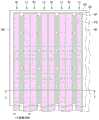
显示面板100包括按照矩阵方式排列的多个像素PXL。像素PXL包括交替排列的多个右眼图像像素列Rv和左眼图像像素列Lv。切换屏障单元BC包括多个屏障和多个空隙区域。切换屏障单元BC的一个空隙区域AP设置在右眼图像像素列Rv和左眼图像像素列Lv之间的边界处。当使右眼图像像素列Rv和左眼图像像素列Lv中的一些暴露时,空隙区域AP具有隙缝形状。在图2中,根据本公开的切换屏障单元BC,屏障区域BR和空隙区域AP没有设置在固定位置处。可以使用液晶单元来配置本公开的切换屏障。当通过供应到液晶单元的电压来驱动液晶时,有效地形成屏障区域BR和空隙区域AP。The
邻近的两个屏障区域BR和设置在两个屏障区域BR之间的一个空隙区域AP形成一个屏障节距。在一个屏障节距内,在横向方向上设置至少两个像素。在该情况下,一个屏障节距包括两个像素,以将图像划分成左眼图像和右眼图像。然而,对于图像被划分成三个图像的情况,可以在一个屏障节距内设置三个像素。Two adjacent barrier regions BR and a gap region AP disposed between the two barrier regions BR form a barrier pitch. Within one barrier pitch, at least two pixels are arranged in the lateral direction. In this case, one barrier pitch includes two pixels to divide the image into a left-eye image and a right-eye image. However, for the case where the image is divided into three images, three pixels can be arranged within one barrier pitch.
参照图3,通过设置在显示面板100上的切换屏障单元BC的空隙区域AP,将右眼图像的光和左眼图像的光彼此划分开。当观察者位于最佳位置时,观察者的右眼只看到右眼图像并且观察者的左眼只看到左眼图像。因此,观察者欣赏到立体图像。3 , the light of the right-eye image and the light of the left-eye image are divided from each other by the gap area AP of the switching barrier unit BC provided on the
在下文中的各种实施方式中,我们将说明根据本公开的用于切换屏障单元BC的用于代表/形成空隙区域AP和屏障BR的电极的各种结构。In various embodiments hereinafter, we will illustrate various structures of electrodes for representing/forming void regions AP and barrier BR for switching barrier cells BC according to the present disclosure.
<第一实施方式><First Embodiment>
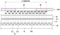
图4是例示了根据本公开的第一实施方式的切换屏障(或移动屏障)结构的截面图。为了方便起见,图4没有示出根据本公开的自动立体3D显示器的整体结构,而例示了切换屏障(主要元件)的结构。图4例示了由替代图3的视差屏障单元BC的液晶面板所表示的切换屏障。设置在切换屏障SB的上部上的屏障BAR实际上没有被包括在切换屏障SB中,而是被包括在例示了由切换屏障SB所代表的空隙区域AP和屏障区域BR的虚拟元件中。4 is a cross-sectional view illustrating a switching barrier (or moving barrier) structure according to the first embodiment of the present disclosure. For convenience, FIG. 4 does not show the overall structure of the autostereoscopic 3D display according to the present disclosure, but illustrates the structure of the switching barrier (main element). FIG. 4 illustrates a switching barrier represented by a liquid crystal panel that replaces the parallax barrier cell BC of FIG. 3 . The barrier BAR provided on the upper part of the switching barrier SB is not actually included in the switching barrier SB, but is included in the dummy element exemplifying the void area AP and the barrier area BR represented by the switching barrier SB.
根据本公开的第一实施方式的切换屏障SB包括表面彼此接合的透明下基板GL和透明上基板GU以及插入到它们之间的液晶层LC。下基板GL包括多个下电极EL。上基板GU包括上电极EU。上电极EU可以具有覆盖上基板GU的整个表面的一片形状并且被供应有电子基本电压。The switching barrier SB according to the first embodiment of the present disclosure includes a transparent lower substrate GL and a transparent upper substrate GU whose surfaces are bonded to each other, and a liquid crystal layer LC interposed therebetween. The lower substrate GL includes a plurality of lower electrodes EL. The upper substrate GU includes the upper electrode EU. The upper electrode EU may have a sheet shape covering the entire surface of the upper substrate GU and be supplied with an electron basic voltage.
以预定距离来排列下电极EL。详细地,下电极EL设置成双层结构。例如,在下基板GL上,以第一预定距离来排列多个第一下电极EL1。第一下电极EL1被钝化层PAS覆盖。在钝化层PAS上,以第二预定距离来排列多个第二下电极EL2。以预定距离来设置第一下电极EL1和第二下电极EL2,使彼此没有交叠。The lower electrodes EL are arranged at a predetermined distance. In detail, the lower electrode EL is provided in a double-layer structure. For example, on the lower substrate GL, a plurality of first lower electrodes EL1 are arranged at a first predetermined distance. The first lower electrode EL1 is covered by the passivation layer PAS. On the passivation layer PAS, a plurality of second lower electrodes EL2 are arranged at a second predetermined distance. The first lower electrode EL1 and the second lower electrode EL2 are arranged at a predetermined distance so as not to overlap each other.
例如,第一下电极EL1中的每一个具有8μm的宽度,并且以8μm的距离(或间隔)来排列第一下电极EL1。另外,在第一钝化层PAS1上,第二下电极EL2中的每一个具有8μm的宽度,并且以8μm距离来排列第二下电极EL2。For example, each of the first lower electrodes EL1 has a width of 8 μm, and the first lower electrodes EL1 are arranged at a distance (or interval) of 8 μm. In addition, on the first passivation layer PAS1, each of the second lower electrodes EL2 has a width of 8 μm, and the second lower electrodes EL2 are arranged at a distance of 8 μm.
分别向第一下电极EL1和第二下电极EL2中的每一个供应电压。然后,因下电极EL和上电极EU之间的电压差,液晶层LC的分子会旋转或改变它们的位置。随着液晶分子的条件改变,形成空隙区域AP和屏障区域BR。A voltage is supplied to each of the first lower electrode EL1 and the second lower electrode EL2, respectively. Then, the molecules of the liquid crystal layer LC rotate or change their positions due to the voltage difference between the lower electrode EL and the upper electrode EU. As the conditions of the liquid crystal molecules change, void regions AP and barrier regions BR are formed.
例如,如图4中所示,当在一个屏障节距内设置12个下电极EL时,在每一个下电极EL处形成一个通道CH。也就是说,在一个屏障节距内连续地设置12个通道CH1至CH12。For example, as shown in FIG. 4, when 12 lower electrodes EL are provided within one barrier pitch, one channel CH is formed at each of the lower electrodes EL. That is, 12 channels CH1 to CH12 are continuously arranged within one barrier pitch.
在该结构下,向第一通道CH1、第二通道CH2、第三通道CH3、第十通道CH10、第十一通道CH11和第十二通道CH12施加0V的电压。另外,向第四通道CH4至第九通道CH9施加10V的电压,使得形成空隙区域AP和屏障区域BR。也就是说,从第四通道CH4至第九通道CH9的区域被限定为切换屏障SB的空隙区域AP。In this structure, a voltage of 0V is applied to the first channel CH1, the second channel CH2, the third channel CH3, the tenth channel CH10, the eleventh channel CH11 and the twelfth channel CH12. In addition, a voltage of 10V is applied to the fourth channel CH4 to the ninth channel CH9, so that the void area AP and the barrier area BR are formed. That is, the area from the fourth channel CH4 to the ninth channel CH9 is defined as the gap area AP of the switching barrier SB.
对于第一实施方式,通过向第一下电极EL1和第二下电极EL2供应不同的电压,可以在每个通道处供应用于驱动液晶层LC的电压,如表1一样。在表1中,向下电极EL供应电压。向上电极EU供应公共电压(例如,0V)。For the first embodiment, by supplying different voltages to the first lower electrode EL1 and the second lower electrode EL2, the voltage for driving the liquid crystal layer LC can be supplied at each channel, as in Table 1. In Table 1, a voltage is supplied to the lower electrode EL. A common voltage (eg, 0V) is supplied to the upper electrode EU.
[表1][Table 1]
在表1中,“-”意指没有对应的下电极。例如,第一通道CH1只具有第一下电极EL1,并且第二通道CH2只具有第二下电极EL2。通过在从第一通道CH1至第三通道CH3分配的第一下电极EL1和第二下电压EL2中的每一个处施加0V,来自第一通道CH1至第三通道CH3的电压被设置成0V。通过相同的方式,来自第十通道CH10至第十二通道CH12的电压被设置成0V。另外,通过在从第四通道CH4至第九通道CH9分配的第一下电极EL1和第二下电压EL2中的每一个处施加10V,来自第四通道CH4至第九通道CH9的电压被设置成10V。然后,具有0V的通道可以形成屏障区域BR并且具有10V的通道可以形成空隙区域AP。In Table 1, "-" means that there is no corresponding lower electrode. For example, the first channel CH1 has only the first lower electrode EL1, and the second channel CH2 has only the second lower electrode EL2. By applying 0V at each of the first lower electrode EL1 and the second lower voltage EL2 distributed from the first to third channels CH1 to CH3, the voltages from the first to third channels CH1 to CH3 are set to 0V. In the same manner, the voltages from the tenth channel CH10 to the twelfth channel CH12 are set to 0V. In addition, by applying 10V at each of the first lower electrode EL1 and the second lower voltage EL2 distributed from the fourth to ninth channels CH4 to CH9, the voltages from the fourth to ninth channels CH4 to CH9 are set to 10V. Then, the channel with 0V may form the barrier region BR and the channel with 10V may form the void region AP.
当需要空隙区域AP移动到其它位置时,可以通过控制供应到下电极EL1和EL2的电压来改变被施加有10V的通道。然后,空隙区域AP可以移动到其它位置。也就是说,图4中示出的空隙区域AP可以移位或移动到左侧或右侧。When the gap area AP needs to be moved to other positions, the channel to which 10V is applied can be changed by controlling the voltages supplied to the lower electrodes EL1 and EL2. Then, the void area AP can be moved to other positions. That is, the gap area AP shown in FIG. 4 may be shifted or moved to the left or right.
在本公开的第一实施方式中,切换屏障SB在一个屏障节距中具有12个通道。根据本公开的第一实施方式的切换屏障SB具有以预定距离顺序排列的多个下电极EL。通过改变下电极EL所限定的通道的分布,可以自由地控制屏障节距的大小。例如,当下电极EL的宽度是8μm时,一个屏障节距将是8(μm)×12(CH)=96μm。又如,当向一个屏障节距分配10个通道时,一个屏障节距将是80μm。如同这种方式,可以根据在切换屏障SB下方的显示面板处设置的像素的像素大小和间隔来控制切换屏障SB。另外,可以自由地改变空隙区域AP。In the first embodiment of the present disclosure, the switching barrier SB has 12 channels in one barrier pitch. The switching barrier SB according to the first embodiment of the present disclosure has a plurality of lower electrodes EL sequentially arranged at a predetermined distance. By changing the distribution of the channels defined by the lower electrode EL, the size of the barrier pitch can be freely controlled. For example, when the width of the lower electrode EL is 8 μm, one barrier pitch will be 8(μm)×12(CH)=96 μm. As another example, when 10 channels are assigned to one barrier pitch, one barrier pitch will be 80 μm. In this way, the switching barrier SB can be controlled according to the pixel size and interval of the pixels provided at the display panel below the switching barrier SB. In addition, the void area AP can be freely changed.
根据本公开的第一实施方式的切换屏障的结构不取决于显示面板。可以根据显示面板的结构来改变屏障节距的大小和空隙区域的大小。另外,可以自由地改变空隙区域的位置。当观察者的位置在横向方向上改变时,通过检测该移动,空隙区域的位置被改变以使得观察者可以一直欣赏到正常的立体图像。The structure of the switching barrier according to the first embodiment of the present disclosure does not depend on the display panel. The size of the barrier pitch and the size of the void area may be changed according to the structure of the display panel. In addition, the positions of the void regions can be freely changed. When the observer's position changes in the lateral direction, by detecting the movement, the position of the void area is changed so that the observer can always enjoy a normal stereoscopic image.
在第一实施方式中,我们说明了在一个屏障节距中具有12个通道的切换屏障。为了增强改变根据第一实施方式的切换屏障的屏障节距大小、空隙区域大小和空隙区域位置的自由度,可以增加通道的数目。In the first embodiment, we illustrate a switching barrier with 12 channels in one barrier pitch. In order to enhance the freedom of changing the barrier pitch size, void area size, and void area position of the switching barrier according to the first embodiment, the number of channels may be increased.
图5是例示了本公开的第一实施方式中的其中通过减小电极的大小来形成更多数目的通道的切换屏障的结构的截面图。如图5中所示,通过将下电极EL的大小减小到4μm,通道的数目可以增加至高达24。结果,能够更精确地改变屏障节距,并且可以更精确地控制空隙区域的大小和位置。5 is a cross-sectional view illustrating a structure of a switching barrier in which a larger number of channels are formed by reducing the size of an electrode in the first embodiment of the present disclosure. As shown in FIG. 5 , by reducing the size of the lower electrode EL to 4 μm, the number of channels can be increased up to 24. As a result, the barrier pitch can be varied more precisely, and the size and location of the void region can be more precisely controlled.
然而,当用诸如4μm的高度精确的图案来形成下电极EL时,由于残留物或异物,导致设置在同一层上的邻近的两个下电极可能彼此接触。例如,邻近的两个第一下电极EL1被电短路。另外,邻近的第一下电极EL1和第二下电极EL2之间的绝缘可能被破坏。结果,一些通道不能够被划分开,使得没有精确地形成通道。However, when the lower electrodes EL are formed with a highly precise pattern such as 4 μm, adjacent two lower electrodes disposed on the same layer may come into contact with each other due to residues or foreign substances. For example, the adjacent two first lower electrodes EL1 are electrically short-circuited. In addition, the insulation between the adjacent first and second lower electrodes EL1 and EL2 may be broken. As a result, some channels cannot be divided, so that the channels are not accurately formed.
利用第一实施方式的结构,受限于通过减小用于形成通道的下电极的大小来制备具有更高的自由度的切换屏障。因此,需要新结构来形成具有用于限定切换屏障的更高的自由度的切换屏障,以更精确地控制空隙区域和增强用于形成通道的电极之间的绝缘性质。With the structure of the first embodiment, it is limited to fabricate a switching barrier with a higher degree of freedom by reducing the size of the lower electrode for forming the channel. Therefore, new structures are needed to form switching barriers with higher degrees of freedom for defining the switching barriers, to more precisely control the void region and to enhance the insulating properties between electrodes used to form channels.
<第二实施方式><Second Embodiment>
在本公开的第二实施方式中,提供了具有以下结构的切换屏障:当在一个屏障节距内增加通道的数目时,在形成通道的邻近的两个电极之间的绝缘没有被破坏。图6是例示了根据本公开的第二实施方式的切换屏障的结构的截面图。In the second embodiment of the present disclosure, there is provided a switching barrier having a structure in which insulation between adjacent two electrodes forming a channel is not broken when the number of channels is increased within one barrier pitch. 6 is a cross-sectional view illustrating a structure of a switching barrier according to a second embodiment of the present disclosure.
根据本公开的第二实施方式的切换屏障包括表面彼此接合的透明下基板GL和透明上基板GU以及插入到它们之间的液晶层LC。下基板GL包括多个下电极EL。上基板GU包括上电极EU。上电极EU可以具有覆盖上基板GU的整个表面的一片形状并且被供应有电子基本电压。The switching barrier according to the second embodiment of the present disclosure includes a transparent lower substrate GL and a transparent upper substrate GU whose surfaces are bonded to each other and a liquid crystal layer LC interposed therebetween. The lower substrate GL includes a plurality of lower electrodes EL. The upper substrate GU includes the upper electrode EU. The upper electrode EU may have a sheet shape covering the entire surface of the upper substrate GU and be supplied with an electron basic voltage.
以预定距离来排列下电极EL。详细地,下电极EL设置成三层结构。例如,在下基板GL上,以第一预定距离来排列多个第一下电极EL1。第一下电极EL1被第一钝化层PAS1覆盖。在第一钝化层PAS1上,以第二预定距离来排列多个第二下电极EL2。第一下电极EL1和第二下电极EL2被设置为彼此不交叠,第一钝化层PAS1处于第一下电极EL1和第二下电极EL2之间。The lower electrodes EL are arranged at a predetermined distance. In detail, the lower electrode EL is provided in a three-layer structure. For example, on the lower substrate GL, a plurality of first lower electrodes EL1 are arranged at a first predetermined distance. The first lower electrode EL1 is covered by the first passivation layer PAS1. On the first passivation layer PAS1, a plurality of second lower electrodes EL2 are arranged at a second predetermined distance. The first lower electrode EL1 and the second lower electrode EL2 are disposed not to overlap each other, and the first passivation layer PAS1 is between the first lower electrode EL1 and the second lower electrode EL2.
第二下电极EL2被第二钝化层PAS2覆盖。在第二钝化层PAS2上,以第三预定距离来排列多个第三下电极EL3。第二下电极EL2和第三下电极EL3被设置为彼此不交叠,第二钝化层PAS2处于第二下电极EL2和第三下电极EL3之间。The second lower electrode EL2 is covered by the second passivation layer PAS2. On the second passivation layer PAS2, a plurality of third lower electrodes EL3 are arranged at a third predetermined distance. The second lower electrode EL2 and the third lower electrode EL3 are disposed not to overlap each other, and the second passivation layer PAS2 is between the second lower electrode EL2 and the third lower electrode EL3.
以预定距离将第一下电极EL1、第二下电极EL2和第三下电极EL3设置为彼此不交叠。例如,在邻近的两个第一下电极EL1之间,设置第二下电极EL2中的一个和第三下电极EL3中的一个。另外,在邻近的两个第二下电极EL2之间,设置第一下电极EL1中的一个和第三下电极EL3中的一个。通过相同的方式,在邻近的两个第三下电极EL3之间,设置第一下电极EL1中的一个和第二下电极EL2中的一个。The first lower electrode EL1, the second lower electrode EL2, and the third lower electrode EL3 are disposed at a predetermined distance so as not to overlap each other. For example, between two adjacent first lower electrodes EL1, one of the second lower electrodes EL2 and one of the third lower electrodes EL3 are provided. In addition, between the adjacent two second lower electrodes EL2, one of the first lower electrodes EL1 and one of the third lower electrodes EL3 are provided. In the same manner, between the adjacent two third lower electrodes EL3, one of the first lower electrodes EL1 and one of the second lower electrodes EL2 are provided.
详细地,第一下电极EL1可以具有4μm的宽度并且以8μm的距离设置。第二下电极EL2可以具有4μm的宽度并且以8μm的距离设置,在第一钝化层PAS1上不与第一下电极EL1交叠。第三下电极EL3可以具有4μm的宽度并且以8μm的距离设置,在第二钝化层PAS2上不与第一下电极EL1和第二下电极EL2交叠。In detail, the first lower electrode EL1 may have a width of 4 μm and be disposed at a distance of 8 μm. The second lower electrode EL2 may have a width of 4 μm and be disposed at a distance of 8 μm without overlapping the first lower electrode EL1 on the first passivation layer PAS1. The third lower electrode EL3 may have a width of 4 μm and be disposed at a distance of 8 μm without overlapping the first and second lower electrodes EL1 and EL2 on the second passivation layer PAS2.
第一下电极EL1、第二下电极EL2和第三下电极EL3中的每一个被分别供应有电压。然后,因下电极EL和上电极EU之间的电压差,液晶层LC的分子会旋转或改变它们的位置。随着液晶分子的条件改变,形成空隙区域AP和屏障区域BR。Each of the first lower electrode EL1, the second lower electrode EL2, and the third lower electrode EL3 is supplied with a voltage, respectively. Then, the molecules of the liquid crystal layer LC rotate or change their positions due to the voltage difference between the lower electrode EL and the upper electrode EU. As the conditions of the liquid crystal molecules change, void regions AP and barrier regions BR are formed.
例如,如图6中所示,当在一个屏障节距内设置24个下电极EL时,在每一个下电极EL处形成一个通道CH。也就是说,在一个屏障节距内连续地设置24个通道CH1至CH24。For example, as shown in FIG. 6, when 24 lower electrodes EL are provided within one barrier pitch, one channel CH is formed at each of the lower electrodes EL. That is, 24 channels CH1 to CH24 are continuously arranged within one barrier pitch.
在这种结构下,向第一通道CH1至第六通道CH6和第十九通道CH19至第二十四通道CH24施加0V的电压。另外,向第七通道CH7至第十八通道CH18施加10V的电压,使得形成空隙区域AP和屏障区域BR。也就是说,从第七通道CH7至第十八通道CH18的区域被限定为切换屏障SB的空隙区域AP。Under this structure, a voltage of 0V is applied to the first to sixth channels CH1 to CH6 and the nineteenth to twenty-fourth channels CH19 to CH24. In addition, a voltage of 10 V is applied to the seventh channel CH7 to the eighteenth channel CH18, so that the void region AP and the barrier region BR are formed. That is, the area from the seventh channel CH7 to the eighteenth channel CH18 is defined as the gap area AP of the switching barrier SB.
对于第二实施方式,通过向第一下电极EL1、第二下电极EL2和第三下电极EL3供应不同的电压,可以在每个通道处供应用于驱动液晶层LC的电压,如表2一样。在表2中,向下电极EL供应电压。向上电极EU供应公共电压(例如,0V)。For the second embodiment, by supplying different voltages to the first lower electrode EL1, the second lower electrode EL2 and the third lower electrode EL3, the voltage for driving the liquid crystal layer LC can be supplied at each channel as in Table 2 . In Table 2, the voltage is supplied to the lower electrode EL. The upper electrode EU is supplied with a common voltage (eg, 0V).
[表2][Table 2]
在表2中,“-”意指没有对应的下电极。例如,第一通道CH1只具有第三下电极EL3。通过向位于第一通道CH1处的第三下电极EL3施加0V,通道电压可被设置成0V。向第七通道CH7和第十八通道CH18施加5V的通道电压的原因是使空隙区域AP和屏障区域BR之间的边界平滑。如有需要,所有通道电压可被设置成0V或10V中的任一个。这里,具有0V的通道可以形成屏障区域BR并且具有10V的通道可以形成空隙区域AP。In Table 2, "-" means that there is no corresponding lower electrode. For example, the first channel CH1 has only the third lower electrode EL3. By applying 0V to the third lower electrode EL3 at the first channel CH1, the channel voltage can be set to 0V. The reason for applying the channel voltage of 5 V to the seventh channel CH7 and the eighteenth channel CH18 is to smooth the boundary between the void region AP and the barrier region BR. All channel voltages can be set to either 0V or 10V if desired. Here, the channel with 0V may form the barrier region BR and the channel with 10V may form the void region AP.
当需要空隙区域AP移动到其它位置时,可以通过控制供应到下电极EL1、EL2和EL3的电压来改变被施加有10V的通道。然后,空隙区域AP可以移动到其它位置。也就是说,图6中示出的空隙区域AP可以移位或者移动到左侧或右侧。When the gap area AP needs to be moved to other positions, the channel to which 10V is applied can be changed by controlling the voltages supplied to the lower electrodes EL1, EL2 and EL3. Then, the void area AP can be moved to other positions. That is, the gap area AP shown in FIG. 6 may be shifted or moved to the left or right.
在本公开的第二实施方式中,切换屏障SB在一个屏障节距中具有24个通道。根据本公开的第二实施方式的切换屏障SB具有以预定距离顺序排列的多个下电极EL。通过改变下电极EL所限定的通道的分布,可以自由地控制屏障节距的大小。例如,当下电极EL的宽度是4μm时,一个屏障节距将是4(μm)×24(CH)=96μm。又如,当向一个屏障节距分配20个通道时,一个屏障节距将是80μm。如同这种方式,可以根据在切换屏障SB下方的显示面板处设置的像素的像素大小和间隔来控制切换屏障SB。另外,可以自由地改变空隙区域AP。In the second embodiment of the present disclosure, the switching barrier SB has 24 channels in one barrier pitch. The switching barrier SB according to the second embodiment of the present disclosure has a plurality of lower electrodes EL sequentially arranged at a predetermined distance. By changing the distribution of the channels defined by the lower electrode EL, the size of the barrier pitch can be freely controlled. For example, when the width of the lower electrode EL is 4 μm, one barrier pitch will be 4(μm)×24(CH)=96 μm. As another example, when 20 channels are assigned to one barrier pitch, one barrier pitch will be 80 μm. In this way, the switching barrier SB can be controlled according to the pixel size and interval of the pixels provided at the display panel below the switching barrier SB. In addition, the void area AP can be freely changed.
另外,在第二实施方式中,下电极EL被设置为分布在这三层中的每一个处。结果,设置在一层上的下电极EL具有足以确保彼此绝缘的距离。例如,具有4μm的宽度的第一下电极EL1彼此以8μm的距离间隔开,不与第二下电极EL2和第三下电极EL3交叠。当形成下电极EL时,它们不会因任何残留物或异物而电短路。In addition, in the second embodiment, the lower electrodes EL are arranged to be distributed at each of the three layers. As a result, the lower electrodes EL provided on one layer have a distance sufficient to ensure insulation from each other. For example, the first lower electrodes EL1 having a width of 4 μm are spaced apart from each other by a distance of 8 μm without overlapping the second and third lower electrodes EL2 and EL3 . When the lower electrodes EL are formed, they are not electrically short-circuited by any residue or foreign matter.
另外,优选的是,设置在空隙区域AP和屏障区域BR的边界处的下电极EL被设置在间隔最远的层处。例如,在第六通道CH6和第七通道CH7被设置在空隙区域AP和屏障区域BR的边界处的情况下,优选的是,第六通道CH6的下电极被分配给第一下电极EL1并且第七通道CH7的下电极被分配给第三下电极EL3。因为在彼此具有不同电压的邻近的两个下电极之间设置了第一钝化层PAS1和第二钝化层PAS2,所以可以确保它们之间具有高的绝缘性质。因为能够防止形成切换屏障的电极之间的绝缘被破坏,所以能够提供正常的立体图像。In addition, it is preferable that the lower electrode EL provided at the boundary of the void region AP and the barrier region BR is provided at the farthest apart layer. For example, in the case where the sixth channel CH6 and the seventh channel CH7 are provided at the boundary of the void area AP and the barrier area BR, it is preferable that the lower electrode of the sixth channel CH6 is assigned to the first lower electrode EL1 and the first The lower electrodes of the seven channels CH7 are assigned to the third lower electrode EL3. Since the first passivation layer PAS1 and the second passivation layer PAS2 are provided between the adjacent two lower electrodes having different voltages from each other, high insulating properties therebetween can be ensured. Since the insulation between the electrodes forming the switching barrier can be prevented from being broken, a normal stereoscopic image can be provided.
<第三实施方式><Third Embodiment>
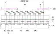
在本公开的第三实施方式中,我们提供了具有即使电极的宽度没有太多地减小也分配较多通道的结构。图7是例示了根据本公开的第三实施方式的切换屏障的结构的截面图。In the third embodiment of the present disclosure, we provide a structure that distributes more channels even if the width of the electrodes is not reduced too much. 7 is a cross-sectional view illustrating a structure of a switching barrier according to a third embodiment of the present disclosure.
根据本公开的第三实施方式的切换屏障包括表面彼此接合的透明下基板GL和透明上基板GU以及插入到它们之间的液晶层LC。下基板GL包括多个下电极EL。上基板GU包括上电极EU。上电极EU可以具有覆盖上基板GU的整个表面的一片形状,并且被供应有电子基本电压。The switching barrier according to the third embodiment of the present disclosure includes a transparent lower substrate GL and a transparent upper substrate GU whose surfaces are bonded to each other and a liquid crystal layer LC interposed therebetween. The lower substrate GL includes a plurality of lower electrodes EL. The upper substrate GU includes the upper electrode EU. The upper electrode EU may have a sheet shape covering the entire surface of the upper substrate GU, and be supplied with an electron basic voltage.
以预定距离来排列具有相同宽度的下电极EL。例如,在下基板GL上,以第一预定距离来排列具有第一宽度的多个第一下电极EL1。第一下电极EL1被第一钝化层PAS1覆盖。在第一钝化层PAS1上,以第二预定距离来排列具有第二宽度的多个第二下电极EL2。第一下电极EL1和第二下电极EL2被设置为彼此不交叠,第一钝化层PAS1处于第一下电极EL1和第二下电极EL2之间。The lower electrodes EL having the same width are arranged at a predetermined distance. For example, on the lower substrate GL, a plurality of first lower electrodes EL1 having a first width are arranged at a first predetermined distance. The first lower electrode EL1 is covered by the first passivation layer PAS1. On the first passivation layer PAS1, a plurality of second lower electrodes EL2 having a second width are arranged at a second predetermined distance. The first lower electrode EL1 and the second lower electrode EL2 are disposed not to overlap each other, and the first passivation layer PAS1 is located between the first lower electrode EL1 and the second lower electrode EL2.
第二下电极EL2被第二钝化层PAS2覆盖。在第二钝化层PAS2上,以第三预定距离来排列具有第三宽度的多个第三下电极EL3。具体地,第三下电极EL3与第一下电极EL1的一半以及第二下电极EL2的一半交叠。The second lower electrode EL2 is covered by the second passivation layer PAS2. On the second passivation layer PAS2, a plurality of third lower electrodes EL3 having a third width are arranged at a third predetermined distance. Specifically, the third lower electrode EL3 overlaps half of the first lower electrode EL1 and half of the second lower electrode EL2.
详细地,第一下电极EL1可以具有8μm的宽度并且以8μm间隔(或距离)排列。第二下电极EL2可以具有8μm的宽度并且在第一钝化层PAS1上以8μm来排列。第三下电极EL3可以具有8μm的宽度并且在第二钝化层PAS2上以8μm来排列。具体地,第三下电极EL3中的每一个与邻近的第一下电极EL1的一半(4μm)以及邻近的第二下电极EL2的一半(4μm)交叠。In detail, the first lower electrodes EL1 may have a width of 8 μm and be arranged at intervals (or distances) of 8 μm. The second lower electrode EL2 may have a width of 8 μm and be arranged at 8 μm on the first passivation layer PAS1 . The third lower electrode EL3 may have a width of 8 μm and be arranged at 8 μm on the second passivation layer PAS2. Specifically, each of the third lower electrodes EL3 overlaps half (4 μm) of the adjacent first lower electrode EL1 and half (4 μm) of the adjacent second lower electrode EL2 .
结果,如图7中所示,在一个屏障节距内形成24个通道。与第一实施方式和第二实施方式不同,在第三实施方式中,这些通道包括第一通道、第二通道、第三通道和第四通道。第一通道只由第一下电极EL1来形成。第四通道只由第二下电极EL2来形成。第二通道由第一下电极EL1和第三下电极EL3之间的交叠部分来形成。第三通道由第二下电极EL1和第三下电极EL3之间的交叠部分来形成。As a result, as shown in FIG. 7, 24 channels are formed within one barrier pitch. Unlike the first and second embodiments, in the third embodiment, the channels include a first channel, a second channel, a third channel, and a fourth channel. The first channel is formed only by the first lower electrode EL1. The fourth channel is formed only by the second lower electrode EL2. The second channel is formed by the overlapping portion between the first lower electrode EL1 and the third lower electrode EL3. The third channel is formed by the overlapping portion between the second lower electrode EL1 and the third lower electrode EL3.
对于第三实施方式,通过向第一下电极EL1、第二下电极EL2和第三下电极EL3供应不同的电压,可以在每个通道处供应用于驱动液晶层LC的电压,如表3一样。在表3中,向下电极EL供应电压。向上电极EU供应公共电压(例如,0V)。For the third embodiment, by supplying different voltages to the first lower electrode EL1, the second lower electrode EL2 and the third lower electrode EL3, the voltage for driving the liquid crystal layer LC can be supplied at each channel as in Table 3 . In Table 3, the voltage is supplied to the lower electrode EL. A common voltage (eg, 0V) is supplied to the upper electrode EU.
[表3][table 3]
在表3中,“-”意指没有对应的下电极。例如,第一通道CH1只具有第一下电极EL1。第二通道CH2具有第一下电极EL1和第三下电极EL3。下电极EL中的任一个被设置为覆盖邻近的两个通道。一个通道只具有一个下电极EL或者设置在不同的层上并且彼此交叠的两个下电极。通过施加到一个下电极的电压或者通过施加到设置在不同的层上并且彼此交叠的两个下电极的电压来决定一个通道电压的电压。为了使空隙区域AP和屏障区域BR之间的边界区域平滑,决定第九通道CH9和第二十通道CH20的通道电压是5V。通道电压为0V的通道形成屏障区域BR,并且通道电压为10V或更大的通道形成空隙区域AP。In Table 3, "-" means that there is no corresponding lower electrode. For example, the first channel CH1 has only the first lower electrode EL1. The second channel CH2 has a first lower electrode EL1 and a third lower electrode EL3. Either one of the lower electrodes EL is arranged to cover the adjacent two channels. One channel has only one lower electrode EL or two lower electrodes arranged on different layers and overlapping each other. The voltage of one channel voltage is determined by the voltage applied to one lower electrode or by the voltage applied to two lower electrodes disposed on different layers and overlapping each other. In order to smooth the boundary area between the void area AP and the barrier area BR, the channel voltage of the ninth channel CH9 and the twentieth channel CH20 is decided to be 5V. A channel with a channel voltage of 0V forms a barrier region BR, and a channel with a channel voltage of 10V or more forms a void region AP.
在第三实施方式中,设置在这三个层当中的两个不同的层处的下电极彼此不交叠,并且设置在另一层处的下电极与设置在这两个层上的电极交叠。因此,存在根据第三实施方式来排列下电极的许多情况。图7示出了第一下电极EL1与第二下电极EL2不交叠的情况。In the third embodiment, the lower electrodes provided at two different layers among the three layers do not overlap with each other, and the lower electrodes provided at the other layer overlap the electrodes provided on the two layers stack. Therefore, there are many cases in which the lower electrodes are arranged according to the third embodiment. FIG. 7 shows a case where the first lower electrode EL1 and the second lower electrode EL2 do not overlap.
图8A和图8B是例示了根据本发明的第三实施方式的具有各种电极阵列结构的各种切换屏障的截面图。对于第三实施例的另一个示例,如图8A中所示,第一下电极EL1不与第三下电极EL3交叠。对于第三实施例的又一个示例,如图8B中所示,第二下电极EL2不与第三下电极EL3交叠。8A and 8B are cross-sectional views illustrating various switching barriers having various electrode array structures according to a third embodiment of the present invention. For another example of the third embodiment, as shown in FIG. 8A, the first lower electrode EL1 does not overlap the third lower electrode EL3. For yet another example of the third embodiment, as shown in FIG. 8B, the second lower electrode EL2 does not overlap the third lower electrode EL3.
虽然已经参照附图详细地描述了本公开的实施方式,但是本领域的技术人员将要理解的是,可以在不改变本公开的技术精神或基本特征的情况下按其它特定形式来实现本公开。因此,应该注意的是,上述实施方式在所有方面都仅仅是例示性的,而不是被理解为限制本公开。本公开的范围由所附的权利要求而非本公开的具体实施方式来限定。在权利要求的含义和范围内进行的所有改变或变型或其等同物应该被理解为落入本公开的范围内。Although the embodiments of the present disclosure have been described in detail with reference to the accompanying drawings, it will be understood by those skilled in the art that the present disclosure may be implemented in other specific forms without changing the technical spirit or essential characteristics of the present disclosure. Therefore, it should be noted that the above-described embodiments are merely illustrative in all respects and should not be construed as limiting the present disclosure. The scope of the disclosure is to be defined by the appended claims rather than the detailed description of the disclosure. All changes or modifications made within the meaning and scope of the claims or their equivalents should be construed as falling within the scope of the present disclosure.
Claims (8)
Translated fromChineseApplications Claiming Priority (2)
| Application Number | Priority Date | Filing Date | Title |
|---|---|---|---|
| KR10-2016-0083088 | 2016-06-30 | ||
| KR1020160083088AKR101800965B1 (en) | 2016-06-30 | 2016-06-30 | Autostereoscopic 3D Image Display |
Publications (2)
| Publication Number | Publication Date |
|---|---|
| CN107561719A CN107561719A (en) | 2018-01-09 |
| CN107561719Btrue CN107561719B (en) | 2020-02-28 |
Family
ID=60807282
Family Applications (1)
| Application Number | Title | Priority Date | Filing Date |
|---|---|---|---|
| CN201710521871.1AActiveCN107561719B (en) | 2016-06-30 | 2017-06-30 | Autostereoscopic 3D Display |
Country Status (3)
| Country | Link |
|---|---|
| US (1) | US10136122B2 (en) |
| KR (1) | KR101800965B1 (en) |
| CN (1) | CN107561719B (en) |
Families Citing this family (2)
| Publication number | Priority date | Publication date | Assignee | Title |
|---|---|---|---|---|
| JP7384419B2 (en)* | 2018-10-16 | 2023-11-21 | 国立大学法人 筑波大学 | Image display device and image display method |
| KR20220157147A (en)* | 2021-05-20 | 2022-11-29 | 삼성전자주식회사 | Method and apparatus for processing an image |
Citations (5)
| Publication number | Priority date | Publication date | Assignee | Title |
|---|---|---|---|---|
| WO2012111427A1 (en)* | 2011-02-16 | 2012-08-23 | Semiconductor Energy Laboratory Co., Ltd. | Display device |
| CN103164071A (en)* | 2011-12-16 | 2013-06-19 | 东莞万士达液晶显示器有限公司 | Switchable touch control stereo image device |
| CN103926751A (en)* | 2013-01-14 | 2014-07-16 | 瀚宇彩晶股份有限公司 | Stereoscopic display device and display method thereof |
| CN105047606A (en)* | 2014-04-29 | 2015-11-11 | 乐金显示有限公司 | Rework method of array substrate for display device and array substrate formed by the method |
| JPWO2014192221A1 (en)* | 2013-05-29 | 2017-02-23 | 株式会社Joled | THIN FILM TRANSISTOR DEVICE, ITS MANUFACTURING METHOD, AND DISPLAY DEVICE |
Family Cites Families (13)
| Publication number | Priority date | Publication date | Assignee | Title |
|---|---|---|---|---|
| KR20080114310A (en)* | 2007-06-27 | 2008-12-31 | 삼성모바일디스플레이주식회사 | Electronic imaging equipment |
| KR100922355B1 (en)* | 2008-03-07 | 2009-10-21 | 삼성모바일디스플레이주식회사 | Electronic imaging equipment |
| KR100893618B1 (en)* | 2008-03-07 | 2009-04-20 | 삼성모바일디스플레이주식회사 | Electronic imaging equipment |
| TW201019018A (en)* | 2008-11-04 | 2010-05-16 | Chunghwa Picture Tubes Ltd | Stereoscopic display device |
| TWI407195B (en)* | 2009-12-30 | 2013-09-01 | Unique Instr Co Ltd | A full-screen three-dimensional image display device |
| KR101324436B1 (en) | 2010-04-02 | 2013-10-31 | 엘지디스플레이 주식회사 | Stereoscopic image display device, mother substrate for the stereoscopic image display device, and fabricating method of the mother substrate |
| GB201019152D0 (en)* | 2010-11-12 | 2010-12-29 | Sec Dep For Business Innovation & Skills The | Force-immune fabry-perot etalon |
| KR101296903B1 (en) | 2010-12-20 | 2013-08-14 | 엘지디스플레이 주식회사 | Stereoscopic image display device and driving method thereof |
| KR101762251B1 (en)* | 2011-03-18 | 2017-07-31 | 삼성디스플레이 주식회사 | Display apparatus and method of driving the same |
| KR101928939B1 (en)* | 2011-11-30 | 2019-03-13 | 삼성디스플레이 주식회사 | 2 dimension/3 dimension switchable display apparatus |
| JP6057647B2 (en)* | 2012-09-27 | 2017-01-11 | 三菱電機株式会社 | Display device |
| KR101981527B1 (en)* | 2012-11-08 | 2019-05-23 | 엘지디스플레이 주식회사 | Autostereoscopic image display and driving method thereof |
| KR20150045135A (en)* | 2013-10-18 | 2015-04-28 | 삼성디스플레이 주식회사 | Stereoscopic image display device and method for driving the same |
- 2016
- 2016-06-30KRKR1020160083088Apatent/KR101800965B1/enactiveActive
- 2017
- 2017-06-30CNCN201710521871.1Apatent/CN107561719B/enactiveActive
- 2017-06-30USUS15/638,915patent/US10136122B2/enactiveActive
Patent Citations (5)
| Publication number | Priority date | Publication date | Assignee | Title |
|---|---|---|---|---|
| WO2012111427A1 (en)* | 2011-02-16 | 2012-08-23 | Semiconductor Energy Laboratory Co., Ltd. | Display device |
| CN103164071A (en)* | 2011-12-16 | 2013-06-19 | 东莞万士达液晶显示器有限公司 | Switchable touch control stereo image device |
| CN103926751A (en)* | 2013-01-14 | 2014-07-16 | 瀚宇彩晶股份有限公司 | Stereoscopic display device and display method thereof |
| JPWO2014192221A1 (en)* | 2013-05-29 | 2017-02-23 | 株式会社Joled | THIN FILM TRANSISTOR DEVICE, ITS MANUFACTURING METHOD, AND DISPLAY DEVICE |
| CN105047606A (en)* | 2014-04-29 | 2015-11-11 | 乐金显示有限公司 | Rework method of array substrate for display device and array substrate formed by the method |
Also Published As
| Publication number | Publication date |
|---|---|
| KR101800965B1 (en) | 2017-11-24 |
| US10136122B2 (en) | 2018-11-20 |
| US20180007348A1 (en) | 2018-01-04 |
| CN107561719A (en) | 2018-01-09 |
Similar Documents
| Publication | Publication Date | Title |
|---|---|---|
| US7825999B2 (en) | Autostereoscopic display | |
| EP2053867B1 (en) | Parallax barrier device and electronic display device | |
| JP5161742B2 (en) | Driving method of 3D image display device | |
| US9838674B2 (en) | Multi-view autostereoscopic display and method for controlling optimal viewing distance thereof | |
| KR101380517B1 (en) | Multi-view autostereoscopic image display and method of controlling optimal viewing distance | |
| KR102284841B1 (en) | Autostereoscopic 3d display device | |
| US20110157696A1 (en) | Display with adaptable parallax barrier | |
| US11095872B2 (en) | Autostereoscopic 3-dimensional display | |
| US9224366B1 (en) | Bendable stereoscopic 3D display device | |
| KR102218777B1 (en) | Autostereoscopic 3d display device | |
| US10986329B2 (en) | Autostereoscopic 3-dimensional display | |
| CN105959674A (en) | 3D display device and method | |
| CN107561719B (en) | Autostereoscopic 3D Display | |
| JP6229044B2 (en) | 3D image display device with fluid barrier pattern | |
| KR102233116B1 (en) | Stereopsis image display device and method of driving the same | |
| US20120033055A1 (en) | Stereoscopic Video Display Apparatus and Display Method | |
| KR102076840B1 (en) | Autostereoscopic image display and driving method thereof | |
| KR102232462B1 (en) | Autostereoscopic 3d display device | |
| KR101992161B1 (en) | Stereoscopic image display and polarity control method thereof | |
| KR20120068126A (en) | 3-dimensional displaying apparatus and driving method thereof | |
| KR102633407B1 (en) | Barrier panel and stereoscopic display device comprising the barrier panel | |
| HK1161753A (en) | Display system and method |
Legal Events
| Date | Code | Title | Description |
|---|---|---|---|
| PB01 | Publication | ||
| PB01 | Publication | ||
| SE01 | Entry into force of request for substantive examination | ||
| SE01 | Entry into force of request for substantive examination | ||
| GR01 | Patent grant | ||
| GR01 | Patent grant |