CN107482304B - mobile device - Google Patents
mobile deviceDownload PDFInfo
- Publication number
- CN107482304B CN107482304BCN201710722644.5ACN201710722644ACN107482304BCN 107482304 BCN107482304 BCN 107482304BCN 201710722644 ACN201710722644 ACN 201710722644ACN 107482304 BCN107482304 BCN 107482304B
- Authority
- CN
- China
- Prior art keywords
- mobile device
- branch
- electrically coupled
- radiating
- antenna structure
- Prior art date
- Legal status (The legal status is an assumption and is not a legal conclusion. Google has not performed a legal analysis and makes no representation as to the accuracy of the status listed.)
- Active
Links
- 230000005855radiationEffects0.000claimsabstractdescription58
- 229910052751metalInorganic materials0.000claimsabstractdescription15
- 239000002184metalSubstances0.000claimsabstractdescription15
- 238000010295mobile communicationMethods0.000claimsdescription16
- 239000004020conductorSubstances0.000claimsdescription9
- 229910052755nonmetalInorganic materials0.000claims2
- 238000000926separation methodMethods0.000claims1
- 238000010586diagramMethods0.000description11
- 238000013461designMethods0.000description9
- 238000004891communicationMethods0.000description8
- 238000004519manufacturing processMethods0.000description6
- 238000000034methodMethods0.000description5
- XEEYBQQBJWHFJM-UHFFFAOYSA-NIronChemical compound[Fe]XEEYBQQBJWHFJM-UHFFFAOYSA-N0.000description4
- 230000009977dual effectEffects0.000description3
- 230000000694effectsEffects0.000description3
- 238000005259measurementMethods0.000description3
- 239000000758substrateSubstances0.000description3
- RYGMFSIKBFXOCR-UHFFFAOYSA-NCopperChemical compound[Cu]RYGMFSIKBFXOCR-UHFFFAOYSA-N0.000description2
- BQCADISMDOOEFD-UHFFFAOYSA-NSilverChemical compound[Ag]BQCADISMDOOEFD-UHFFFAOYSA-N0.000description2
- 230000002411adverseEffects0.000description2
- 229910045601alloyInorganic materials0.000description2
- 239000000956alloySubstances0.000description2
- 229910052782aluminiumInorganic materials0.000description2
- XAGFODPZIPBFFR-UHFFFAOYSA-NaluminiumChemical compound[Al]XAGFODPZIPBFFR-UHFFFAOYSA-N0.000description2
- 229910052802copperInorganic materials0.000description2
- 239000010949copperSubstances0.000description2
- 238000011161developmentMethods0.000description2
- 229910052742ironInorganic materials0.000description2
- 239000012811non-conductive materialSubstances0.000description2
- 229910052709silverInorganic materials0.000description2
- 239000004332silverSubstances0.000description2
- RNFJDJUURJAICM-UHFFFAOYSA-N2,2,4,4,6,6-hexaphenoxy-1,3,5-triaza-2$l^{5},4$l^{5},6$l^{5}-triphosphacyclohexa-1,3,5-trieneChemical compoundN=1P(OC=2C=CC=CC=2)(OC=2C=CC=CC=2)=NP(OC=2C=CC=CC=2)(OC=2C=CC=CC=2)=NP=1(OC=1C=CC=CC=1)OC1=CC=CC=C1RNFJDJUURJAICM-UHFFFAOYSA-N0.000description1
- 101001045744Sus scrofa Hepatocyte nuclear factor 1-betaProteins0.000description1
- 239000000969carrierSubstances0.000description1
- 239000002131composite materialSubstances0.000description1
- 239000002537cosmeticSubstances0.000description1
- 230000008878couplingEffects0.000description1
- 238000010168coupling processMethods0.000description1
- 238000005859coupling reactionMethods0.000description1
- 238000005516engineering processMethods0.000description1
- 239000003063flame retardantSubstances0.000description1
- 230000007774longtermEffects0.000description1
- 239000000463materialSubstances0.000description1
- 238000012986modificationMethods0.000description1
- 230000004048modificationEffects0.000description1
Images


Classifications
- H—ELECTRICITY
- H01—ELECTRIC ELEMENTS
- H01Q—ANTENNAS, i.e. RADIO AERIALS
- H01Q1/00—Details of, or arrangements associated with, antennas
- H01Q1/12—Supports; Mounting means
- H01Q1/22—Supports; Mounting means by structural association with other equipment or articles
- H01Q1/24—Supports; Mounting means by structural association with other equipment or articles with receiving set
- H01Q1/241—Supports; Mounting means by structural association with other equipment or articles with receiving set used in mobile communications, e.g. GSM
- H01Q1/242—Supports; Mounting means by structural association with other equipment or articles with receiving set used in mobile communications, e.g. GSM specially adapted for hand-held use
- H01Q1/243—Supports; Mounting means by structural association with other equipment or articles with receiving set used in mobile communications, e.g. GSM specially adapted for hand-held use with built-in antennas
- H—ELECTRICITY
- H01—ELECTRIC ELEMENTS
- H01Q—ANTENNAS, i.e. RADIO AERIALS
- H01Q13/00—Waveguide horns or mouths; Slot antennas; Leaky-waveguide antennas; Equivalent structures causing radiation along the transmission path of a guided wave
- H01Q13/10—Resonant slot antennas
- H—ELECTRICITY
- H01—ELECTRIC ELEMENTS
- H01Q—ANTENNAS, i.e. RADIO AERIALS
- H01Q5/00—Arrangements for simultaneous operation of antennas on two or more different wavebands, e.g. dual-band or multi-band arrangements
- H01Q5/30—Arrangements for providing operation on different wavebands
- H01Q5/307—Individual or coupled radiating elements, each element being fed in an unspecified way
- H01Q5/342—Individual or coupled radiating elements, each element being fed in an unspecified way for different propagation modes
- H01Q5/357—Individual or coupled radiating elements, each element being fed in an unspecified way for different propagation modes using a single feed point
- H01Q5/364—Creating multiple current paths
- H01Q5/371—Branching current paths
- H—ELECTRICITY
- H01—ELECTRIC ELEMENTS
- H01Q—ANTENNAS, i.e. RADIO AERIALS
- H01Q9/00—Electrically-short antennas having dimensions not more than twice the operating wavelength and consisting of conductive active radiating elements
- H01Q9/04—Resonant antennas
- H01Q9/30—Resonant antennas with feed to end of elongated active element, e.g. unipole
- H01Q9/42—Resonant antennas with feed to end of elongated active element, e.g. unipole with folded element, the folded parts being spaced apart a small fraction of the operating wavelength
- H—ELECTRICITY
- H05—ELECTRIC TECHNIQUES NOT OTHERWISE PROVIDED FOR
- H05K—PRINTED CIRCUITS; CASINGS OR CONSTRUCTIONAL DETAILS OF ELECTRIC APPARATUS; MANUFACTURE OF ASSEMBLAGES OF ELECTRICAL COMPONENTS
- H05K1/00—Printed circuits
- H05K1/16—Printed circuits incorporating printed electric components, e.g. printed resistor, capacitor, inductor
- H05K1/165—Printed circuits incorporating printed electric components, e.g. printed resistor, capacitor, inductor incorporating printed inductors
- H—ELECTRICITY
- H05—ELECTRIC TECHNIQUES NOT OTHERWISE PROVIDED FOR
- H05K—PRINTED CIRCUITS; CASINGS OR CONSTRUCTIONAL DETAILS OF ELECTRIC APPARATUS; MANUFACTURE OF ASSEMBLAGES OF ELECTRICAL COMPONENTS
- H05K2201/00—Indexing scheme relating to printed circuits covered by H05K1/00
- H05K2201/10—Details of components or other objects attached to or integrated in a printed circuit board
- H05K2201/10007—Types of components
- H05K2201/10098—Components for radio transmission, e.g. radio frequency identification [RFID] tag, printed or non-printed antennas
- Y—GENERAL TAGGING OF NEW TECHNOLOGICAL DEVELOPMENTS; GENERAL TAGGING OF CROSS-SECTIONAL TECHNOLOGIES SPANNING OVER SEVERAL SECTIONS OF THE IPC; TECHNICAL SUBJECTS COVERED BY FORMER USPC CROSS-REFERENCE ART COLLECTIONS [XRACs] AND DIGESTS
- Y10—TECHNICAL SUBJECTS COVERED BY FORMER USPC
- Y10T—TECHNICAL SUBJECTS COVERED BY FORMER US CLASSIFICATION
- Y10T29/00—Metal working
- Y10T29/49—Method of mechanical manufacture
- Y10T29/49002—Electrical device making
- Y10T29/49016—Antenna or wave energy "plumbing" making
- Y10T29/49018—Antenna or wave energy "plumbing" making with other electrical component
Landscapes
- Engineering & Computer Science (AREA)
- Computer Networks & Wireless Communication (AREA)
- Support Of Aerials (AREA)
- Waveguide Aerials (AREA)
- Telephone Set Structure (AREA)
- Manufacturing & Machinery (AREA)
- Microelectronics & Electronic Packaging (AREA)
Abstract
Translated fromChinese
Description
Translated fromChinese本发明是中国发明专利申请(申请号:201410052368.2,申请日:2014年2月14日,发明名称:移动装置及其制造方法)的分案申请。The present invention is a divisional application of a Chinese invention patent application (application number: 201410052368.2, application date: February 14, 2014, invention title: mobile device and its manufacturing method).
技术领域technical field
本发明涉及一种移动装置,特别是涉及一种具有多频天线结构(Multi-bandAntenna Structure)的移动装置。The present invention relates to a mobile device, in particular to a mobile device with a multi-band antenna structure (Multi-band Antenna Structure).
背景技术Background technique
随着移动通讯技术的发达,移动装置在近年日益普遍,常见的例如:手提式电脑、移动电话、多媒体播放器以及其他混合功能的携带型电子装置。为了满足人们的需求,移动装置通常具有无线通讯的功能。有些涵盖长距离的无线通讯范围,例如:移动电话使用2G、3G、LTE(Long Term Evolution)系统及其所使用700MHz、850MHz、900MHz、1800MHz、1900MHz、2100MHz、2300MHz以及2500MHz的频带进行通讯,而有些则涵盖短距离的无线通讯范围,例如:Wi-Fi、Bluetooth以及WiMAX(Worldwide Interoperability for MicrowaveAccess)系统使用2.4GHz、3.5GHz、5.2GHz和5.8GHz的频带进行通讯。With the development of mobile communication technology, mobile devices have become increasingly common in recent years, such as laptop computers, mobile phones, multimedia players, and other portable electronic devices with mixed functions. In order to meet people's needs, mobile devices usually have the function of wireless communication. Some cover long-distance wireless communication range, such as: mobile phones use 2G, 3G, LTE (Long Term Evolution) systems and their use of 700MHz, 850MHz, 900MHz, 1800MHz, 1900MHz, 2100MHz, 2300MHz and 2500MHz frequency bands for communication, while Some cover the short-distance wireless communication range, for example: Wi-Fi, Bluetooth and WiMAX (Worldwide Interoperability for MicrowaveAccess) systems use 2.4GHz, 3.5GHz, 5.2GHz and 5.8GHz frequency bands for communication.
天线为具有无线通讯功能的移动装置中不可或缺的元件。由于近年来移动装置的设计趋势都朝向轻薄化发展,如何将可支持多频操作的天线妥善地设计于移动装置的有限内部空间中,已成为现今天线设计者的一大挑战。Antennas are indispensable components in mobile devices with wireless communication functions. As the design trend of mobile devices in recent years has been toward thinness and lightness, how to properly design an antenna that can support multi-frequency operation in the limited internal space of the mobile device has become a major challenge for antenna designers today.
发明内容SUMMARY OF THE INVENTION
在一示范实施例中,本发明提供一种移动装置,包括:一外壳;以及一外观金属部,设置于该外壳的一外表面上,其中一第一辐射支路和一第二辐射支路都属于该外观金属部的一部分;其中该第一辐射支路和该第二辐射支路是共同形成一多频天线结构。In an exemplary embodiment, the present invention provides a mobile device, comprising: a casing; and an appearance metal part disposed on an outer surface of the casing, wherein a first radiation branch and a second radiation branch All belong to a part of the appearance metal part; wherein the first radiation branch and the second radiation branch together form a multi-frequency antenna structure.
附图说明Description of drawings
图1为本发明一实施例所述的移动装置的示意图;FIG. 1 is a schematic diagram of a mobile device according to an embodiment of the present invention;
图2A为本发明一实施例所述的移动装置的多频天线结构经由第一馈入点所馈入时的电压驻波比(Voltage Standing Wave Radio,VSWR)图;2A is a diagram of a Voltage Standing Wave Ratio (VSWR) when a multi-frequency antenna structure of a mobile device is fed through a first feeding point according to an embodiment of the present invention;
图2B为本发明一实施例所述的移动装置的多频天线结构经由第二馈入点所馈入时的电压驻波比图;2B is a voltage standing wave ratio diagram when the multi-frequency antenna structure of the mobile device is fed through a second feeding point according to an embodiment of the present invention;
图3为本发明一实施例所述的移动装置的天线原理的示意图;3 is a schematic diagram of an antenna principle of a mobile device according to an embodiment of the present invention;
图4为本发明一实施例所述的移动装置的示意图;4 is a schematic diagram of a mobile device according to an embodiment of the present invention;
图5A为本发明一实施例所述的移动装置的顶部视图;5A is a top view of a mobile device according to an embodiment of the present invention;
图5B为本发明一实施例所述的移动装置的正面视图;5B is a front view of the mobile device according to an embodiment of the present invention;
图5C为本发明一实施例所述的移动装置的背面视图;5C is a rear view of the mobile device according to an embodiment of the present invention;
图6为本发明一实施例所述的移动装置的示意图;6 is a schematic diagram of a mobile device according to an embodiment of the present invention;
图7为本发明一实施例所述的移动装置的制造方法的流程图。FIG. 7 is a flowchart of a method for manufacturing a mobile device according to an embodiment of the present invention.
符号说明Symbol Description
100、400、500、600~移动装置; 110~接地面;100, 400, 500, 600 ~ mobile device; 110 ~ ground plane;
120~接地支路; 130~连接部;120~grounding branch; 130~connecting part;
140~第一辐射支路; 141~第一辐射支路的弯折末端;140~the first radiation branch; 141~the bent end of the first radiation branch;
150~第二辐射支路; 160~第一开口槽孔;150~the second radiation branch; 160~the first opening slot;
170~第二开口槽孔; 181~第一同轴电缆线;170~the second opening slot; 181~the first coaxial cable;
182~第二同轴电缆线; 191~第一信号源;182~the second coaxial cable; 191~the first signal source;
192~第二信号源; 451~短路部;192~Second signal source; 451~Short circuit part;
452~封闭开孔; 510~外壳;452~closed opening; 510~shell;
511~外壳的狭长间隙; 520~外观金属部;511~The narrow and long gap of the shell; 520~Appearance metal part;
530~显示模块; 540~触控模块;530~display module; 540~touch module;
550~电源键; 560~耳机插孔;550~Power button; 560~Headphone jack;
570~麦克风收音孔; 630~电子零件;570~Microphone sound-receiving hole; 630~Electronic parts;
650~布线区域;650 ~ wiring area;
A、B、C、D、E、G、H、I~共振路径上的点;A, B, C, D, E, G, H, I ~ points on the resonance path;
F1~第一馈入点;F1~the first feed point;
F2~第二馈入点;F2~the second feed point;
FB1~移动通讯频带;FB1 ~ mobile communication frequency band;
FB2~全球卫星定位系统频带;FB2~GPS frequency band;
GC1、GC2~第二辐射支路和第一辐射支路的间距;GC1, GC2 to the distance between the second radiation branch and the first radiation branch;
W1~第一开口槽孔的宽度;W1~the width of the first opening slot;
W2~第二开口槽孔的宽度; W3~第一辐射支路的宽度;W2~the width of the second opening slot; W3~the width of the first radiation branch;
W4~第二辐射支路的宽度; W5~连接部的宽度。W4~the width of the second radiation branch; W5~the width of the connecting portion.
具体实施方式Detailed ways
为让本发明的目的、特征和优点能更明显易懂,下文特举出本发明的具体实施例,并配合所附的附图,作详细说明如下。In order to make the objects, features and advantages of the present invention more clearly understood, the following specific embodiments of the present invention are given and described in detail in conjunction with the accompanying drawings.
图1显示根据本发明一实施例所述的移动装置100的示意图,特别是移动装置100的天线结构的平面展开示意图。举例来说,移动装置100可以是一智能型手机(SmartPhone)、一平板电脑(Tablet Computer),或是一笔记型电脑(Notebook Computer)。如图1所示,移动装置100至少包括:一接地面110、一接地支路120、一连接部130、一第一辐射支路140,以及一第二辐射支路150。移动装置100的前述元件可用导体材料制成,例如:银、铜、铝、铁,或是其合金。移动装置100的前述元件或部分元件还可设置于一介质基板(Dielectric Substrate)上,例如:一FR4(Flame Retardant 4)基板、一系统电路板,或是一软硬复合板。接地支路120耦接至接地面110,其中接地支路120和接地面110大致包围一第一开口槽孔(Open Slot)160。第一辐射支路140经由连接部130电性耦接至接地支路120,其中第一辐射支路140和接地支路120大致包围一第二开口槽孔170。第二辐射支路150设置于第二开口槽孔170内,并耦接至接地支路120。在优选实施例中,接地支路120、连接部130、第一辐射支路140以及第二辐射支路150共同形成一多频天线结构(Multi-band AntennaStructure)。移动装置100还可包括其他必要元件,例如:一触控输入模块、一显示模块、一处理器模块、一控制模块,以及一供电模块等等(未显示)。必须理解的是,虽然图1显示平面化的一多频天线结构,但在其他实施例中,该多频天线结构也可改为一立体结构,而其内的各元件还可分别设置或形成于不同的载体上,例如:分别设置于一印刷电路板(PrintedCircuit Board,PCB)、一软性电路板(Flexible Printed Circuit Board,FPCB)上,以及一壳体上(未显示)。FIG. 1 shows a schematic diagram of a
前述的多频天线结构具有一第一馈入点F1和一第二馈入点F2。在一些实施例中,第一馈入点F1位于接地支路120上(例如:可大致位于接地支路120的中央处),而第二馈入点F2位于第二辐射支路150上(例如:可大致位于第二辐射支路150的中央处)。第一馈入点F1可经由一第一同轴电缆线(Coaxial Cable)181耦接至一第一信号源191,而第二馈入点F2可经由一第二同轴电缆线182耦接至一第二信号源192。第一信号源191和第二信号源192可以是相异的二射频(Radio Frequency)模块,其可分别用于产生不同频率的馈入信号,以激发前述的多频天线结构。The aforementioned multi-frequency antenna structure has a first feeding point F1 and a second feeding point F2. In some embodiments, the first feeding point F1 is located on the grounding branch 120 (eg, may be located approximately at the center of the grounding branch 120 ), and the second feeding point F2 is located on the second radiation branch 150 (eg, may be located at the center of the grounding branch 120 ) : may be located approximately at the center of the second radiation branch 150). The first feeding point F1 can be coupled to a
在一些实施例中,第一开口槽孔160和第二开口槽孔170分别大致为一直条形。第一开口槽孔160可以大致平行于第二开口槽孔170,而第一开口槽孔160和第二开口槽孔170的二开口端可以大致朝向相反方向。第二开口槽孔170的宽度W2可以远大于第一开口槽孔160的宽度W1。在一些实施例中,接地支路120、连接部130,以及第一辐射支路140所形成的一组合大致为一倒U字形。在一些实施例中,第一辐射支路140还具有一弯折末端141,其中弯折末端141朝向第二开口槽孔170的一开口端作延伸,使得第二开口槽孔170具有一不等宽结构。在其他实施例中,第一辐射支路140也可改为不具有任何弯折末端且大致为一直条形,使得第二开口槽孔170具有一等宽结构(未显示)。在一些实施例中,第二辐射支路150大致为一倒L字形。第二辐射支路150的宽度W4可以远小于第一辐射支路140的宽度W3。In some embodiments, the first
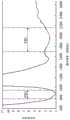
图2A显示根据本发明一实施例所述的移动装置100的该多频天线结构经由第一馈入点F1所馈入时的电压驻波比(Voltage Standing Wave Radio,VSWR)图,其中横轴代表操作频率(MHz),而纵轴代表电压驻波比。根据图2A的测量结果,当该多频天线结构由第一信号源191所激发时,该多频天线结构将涵盖一移动通讯频带FB1。在一些实施例中,移动通讯频带FB1的低频部分约介于791MHz至960MHz之间,而移动通讯频带FB1的高频部分约介于1710MHz至2170MHz之间。2A shows a voltage standing wave ratio (VSWR) diagram when the multi-frequency antenna structure of the
图2B显示根据本发明一实施例所述的移动装置100的该多频天线结构经由第二馈入点F2所馈入时的电压驻波比图,其中横轴代表操作频率(MHz),而纵轴代表电压驻波比。根据图2B的测量结果,当该多频天线结构由第二信号源192所激发时,该多频天线结构将涵盖一定位系统频带FB2。举例来说,前述的定位系统可以是一全球卫星定位系统(GlobalPositioning System,GPS)、一全球导航卫星系统(Global Navigation SatelliteSystem,GNSS)、一北斗卫星导航系统(BeiDou Navigation Satellite System,BDS),或是一伽利略定位系统(Galileo Positioning System)。以下的实施例是以全球卫星定位系统来做说明。在一些实施例中,前述的定位系统频带FB2约介于1560MHz至1615MHz之间。因此,本发明的该多频天线结构至少可支持LTE Band 20/GSM850/GSM900/GPS/DCS1800/PCS1900/UMTS的多频带操作。2B shows a VSWR diagram of the multi-frequency antenna structure of the
图3显示根据本发明一实施例所述的移动装置100的天线原理的平面展开示意图。请一并参考图2A、图2B、图3。当该多频天线结构经由第一馈入点F1所馈入时,从点A经过点B、C、D至点E的一第一共振路径可以激发产生移动通讯频带FB1的低频部分,而从第一馈入点F1至点B的一第二共振路径可以激发产生移动通讯频带FB1的高频部分(其中点A为接地点)。天线设计者可用下列方式微调移动通讯频带FB1:通过改变该第一共振路径和该第二共振路径的长度可以调整移动通讯频带FB1的共振频率;通过改变第一开口槽孔160的宽度W1可以调整移动通讯频带FB1的频宽和效率;通过增加第一辐射支路140的宽度W3可使得移动通讯频带FB1的共振频率往低频偏移;以及通过改变连接部130的宽度W5可以调整移动通讯频带FB1的低频部分。另一方面,当该多频天线结构经由第二馈入点F2所馈入时,从点G经过点H至点I的一第三共振路径可以激发产生全球卫星定位系统频带FB2。天线设计者可用下列方式微调全球卫星定位系统频带FB2:通过改变该第三共振路径的长度可以调整全球卫星定位系统频带FB2的共振频率;以及通过改变第二辐射支路150的连接点的位置(亦即,点G,其为接地点)可以调整全球卫星定位系统频带FB2的共振频率。另外,第二辐射支路150和第一辐射支路140的二间距GC1、GC2都应设计为大于0.5mm,如此可降低第二辐射支路150和第一辐射支路140之间的互相耦合效应,从而可维持该多频天线结构的良好天线效率。FIG. 3 is a schematic expanded plan view of an antenna principle of the
在一些实施例中,该多频天线结构的总长度约为67mm,总宽度约为11mm,总高度约为9mm。根据一些测量结果,该多频天线结构于移动通讯频带FB1中的天线效率都大于49.6%,而该多频天线结构于全球卫星定位系统频带FB2中的天线效率都大于37.1%,其已可符合实际应用需要。本发明将双馈入部和双辐射体同时整合入单一天线结构中以涵盖双宽频操作,如此天线结构将具有小尺寸和多功能的特色。和传统设计方式相比,本发明至少具有下列优点:(1)节省移动装置的内部设计空间;(2)可省去滤波元件;(3)减少元件损耗;以及(4)降低制造成本及系统复杂度,故本发明非常适合应用于各种小型化的移动通讯装置。In some embodiments, the overall length of the multi-frequency antenna structure is about 67 mm, the overall width is about 11 mm, and the overall height is about 9 mm. According to some measurement results, the antenna efficiency of the multi-frequency antenna structure in the mobile communication frequency band FB1 is greater than 49.6%, and the antenna efficiency of the multi-frequency antenna structure in the GPS frequency band FB2 is greater than 37.1%, which can meet the practical application needs. The present invention simultaneously integrates dual feeds and dual radiators into a single antenna structure to cover dual broadband operation, so that the antenna structure will have the characteristics of small size and multi-functionality. Compared with the traditional design method, the present invention has at least the following advantages: (1) saving the internal design space of the mobile device; (2) eliminating the filter element; (3) reducing the loss of the element; and (4) reducing the manufacturing cost and system Therefore, the present invention is very suitable to be applied to various miniaturized mobile communication devices.
图4显示根据本发明一实施例所述的移动装置400的示意图。图4基本上与图1相似,同样是天线结构的平面展开示意图,然而两者的差异在于,图4的移动装置400还包括一短路部451。短路部451可用导体材料制成,例如:银、铜、铝、铁,或是其合金。在图4的移动装置400中,第二辐射支路150还经由短路部451电性耦接至连接部130,使得第二辐射支路150、短路部451、连接部130,以及接地支路120之间形成一封闭开孔452。封闭开孔452可以大致为一矩形或一圆形。封闭开孔452可用于容纳一些外观元件的设计或电子零件的配置。在其他实施例中,封闭开孔452也可改由导体材料所填满。图4的移动装置400的其余特征都与图1的移动装置100相似,故此二实施例均可达成相似的操作效果。FIG. 4 shows a schematic diagram of a
图5A显示根据本发明一实施例所述的移动装置500的顶部视图。图5B显示根据本发明一实施例所述的移动装置500的正面视图。图5C显示根据本发明一实施例所述的移动装置500的背面视图。请一并参考图5A、图5B、图5C。图5A、图5B、图5C基本上与图1相似,两者的差异在于,图5A、图5B、图5C用于说明图1的立体天线结构,其中移动装置500还包括一外壳510、一外观金属部520、一显示模块530,以及一触控模块540。外壳510可以包括移动装置500的背盖及边框部分,并可用导体材料或是非导体材料制成。移动装置500的接地面110、接地支路120,以及连接部130都设置于外壳510的内部(未显示)。外壳510还可具有一狭长间隙511,其中狭长间隙511可以大致对齐于接地支路120和接地面110之间的第一开口槽孔160。外壳510的狭长间隙511还可由非导体材料所填满,例如:塑胶。外观金属部520设置于外壳510的一外表面上(例如:顶部表面),其中移动装置500的第一辐射支路140和第二辐射支路150都属于外观金属部520的一部分。连接部130可以是一金属弹片(Metal Spring)或一顶针(Pogo Pin),其可用于电性耦接一介质基板上的接地支路120(未显示)至外壳510上的第一辐射支路140和第二辐射支路150。在一些实施例中,第一辐射支路140是由移动装置500的顶部延伸至移动装置500的背部,并配置于外壳510上。在另一些实施例中,当外壳510由导体材料所制成时,第一辐射支路140与外壳510作结合,或是形成外壳510的一部分。另外,第二辐射支路150也可与导体材料所制成的外壳510作结合,或是形成外壳510的另一部分。换言之,外壳510也可与外观金属部520整合为单一元件。第二辐射支路150较佳是位于移动装置500的顶部并朝向天空方向,因此移动装置500的一多频天线结构将可更容易接收及传送全球卫星定位系统频带FB2的信号。另外,由于外观金属部520整合于该多频天线结构之中,故外观金属部520将不会对于该多频天线结构的辐射性能造成负面影响。图5A、图5B、图5C的移动装置500的其余特征都与图1的移动装置100相似,故此二实施例均可达成相似的操作效果。必须注意的是,如图5A所示,外观金属部520所形成的区域内仍有一些非金属区域,而这些非金属区域内可配置其它电子零件,例如:一电源键550、一耳机插孔560、一麦克风收音孔570、一插槽,或是一连接构件等等(未显示),其可依不同的设计做调整。在另一些实施例中,该多频天线结构也可配置于移动装置500的底部,其详细的元件配置与设计则不再赘述。FIG. 5A shows a top view of a
图6显示根据本发明一实施例所述的移动装置600的平面展开示意图。图6基本上与图1相似,同样是天线结构的平面展开示意图,然而两者的差异在于,图6的移动装置600还包括一或多个电子零件630,其中该等电子零件630设置于移动装置600的接地支路120或(且)接地面110上。例如,该等电子零件630可以包括一扬声器(Speaker)、一相机(Camera),或(且)一耳机插孔(Audio Jack)。该等电子零件630可视为移动装置600的一多频天线结构的一部分,因此它们将不会对于该多频天线结构的辐射性能造成负面影响。由于该多频天线结构可承载该等电子零件630并做适切地整合,此设计方式将可有效地节省移动装置600的内部设计空间。该等电子零件630还可经由接地面110上的一布线区域650耦接至一处理器模块与一控制模块(未显示)。图6的移动装置600的其余特征都与图1的移动装置100相似,故此二实施例均可达成相似的操作效果。FIG. 6 is a schematic diagram illustrating a plan development of a
图7显示根据本发明一实施例所述的移动装置的制造方法的流程图。该制造方法包括下列步骤。在步骤S710,提供一接地面。在步骤S720,将一接地支路耦接至该接地面,其中该接地支路和该接地面大致包围一第一开口槽孔。在步骤S730,将一第一辐射支路经由一连接部电性耦接至该接地支路,其中该第一辐射支路和该接地支路大致包围一第二开口槽孔。在步骤S740,在该第二开口槽孔内设置一第二辐射支路,并将该第二辐射支路耦接至该接地支路。在步骤S750,利用该接地支路、该连接部、该第一辐射支路,以及该第二辐射支路来形成一多频天线结构。必须理解的是,以上步骤无须依次序执行,而图1至图6的实施例的每一装置特征均可套用至图7所述的移动装置的制造方法。FIG. 7 shows a flowchart of a method for manufacturing a mobile device according to an embodiment of the present invention. The manufacturing method includes the following steps. In step S710, a ground plane is provided. In step S720, a ground branch is coupled to the ground plane, wherein the ground branch and the ground plane substantially surround a first opening slot. In step S730, a first radiation branch is electrically coupled to the ground branch through a connecting portion, wherein the first radiation branch and the ground branch substantially surround a second opening slot. In step S740, a second radiation branch is disposed in the second opening slot, and the second radiation branch is coupled to the ground branch. In step S750, a multi-frequency antenna structure is formed by using the ground branch, the connection portion, the first radiation branch, and the second radiation branch. It must be understood that the above steps do not need to be performed in sequence, and each device feature of the embodiments of FIG. 1 to FIG. 6 can be applied to the manufacturing method of the mobile device described in FIG. 7 .
值得注意的是,以上所述的元件尺寸、元件形状、以及频率范围均非为本发明的限制条件。天线设计者可以根据不同需要调整这些设定值。另外,本发明的通讯装置及天线结构并不仅限于图1至图7所图示的状态。本发明可以仅包括图1至图7的任何一或多个实施例的任何一或多项特征。换言之,并非所有图示的特征均须同时实施于本发明的通讯装置及天线结构当中。It should be noted that the above-mentioned element size, element shape, and frequency range are not limitations of the present invention. Antenna designers can adjust these settings according to different needs. In addition, the communication device and the antenna structure of the present invention are not limited to the states shown in FIGS. 1 to 7 . The present invention may include only any one or more of the features of any one or more of the embodiments of FIGS. 1-7 . In other words, not all of the illustrated features need to be simultaneously implemented in the communication device and the antenna structure of the present invention.
在本说明书以及权利要求中的序数,例如「第一」、「第二」、「第三」等等,彼此之间并没有顺序上的先后关系,其仅用于标示区分两个具有相同名字的不同元件。The ordinal numbers in this specification and the claims, such as "first", "second", "third", etc., do not have a sequential relationship with each other, and are only used to identify two people with the same name. different components.
虽然结合以上优选实施例公开了本发明,然而其并非用以限定本发明的范围,任何熟悉此项技术者,在不脱离本发明的精神和范围内,可做些许的更动与润饰,因此本发明的保护范围应当以附上的权利要求所界定的为准。Although the present invention has been disclosed in conjunction with the above preferred embodiments, it is not intended to limit the scope of the present invention. Anyone skilled in the art can make some changes and modifications without departing from the spirit and scope of the present invention. Therefore, The scope of protection of the present invention should be defined by the appended claims.
Claims (26)
Applications Claiming Priority (3)
| Application Number | Priority Date | Filing Date | Title |
|---|---|---|---|
| US14/157,126 | 2014-01-16 | ||
| US14/157,126US9774073B2 (en) | 2014-01-16 | 2014-01-16 | Mobile device and multi-band antenna structure therein |
| CN201410052368.2ACN104795623B (en) | 2014-01-16 | 2014-02-14 | Mobile device and manufacturing method thereof |
Related Parent Applications (1)
| Application Number | Title | Priority Date | Filing Date |
|---|---|---|---|
| CN201410052368.2ADivisionCN104795623B (en) | 2014-01-16 | 2014-02-14 | Mobile device and manufacturing method thereof |
Publications (2)
| Publication Number | Publication Date |
|---|---|
| CN107482304A CN107482304A (en) | 2017-12-15 |
| CN107482304Btrue CN107482304B (en) | 2020-11-24 |
Family
ID=53484811
Family Applications (2)
| Application Number | Title | Priority Date | Filing Date |
|---|---|---|---|
| CN201710722644.5AActiveCN107482304B (en) | 2014-01-16 | 2014-02-14 | mobile device |
| CN201410052368.2AActiveCN104795623B (en) | 2014-01-16 | 2014-02-14 | Mobile device and manufacturing method thereof |
Family Applications After (1)
| Application Number | Title | Priority Date | Filing Date |
|---|---|---|---|
| CN201410052368.2AActiveCN104795623B (en) | 2014-01-16 | 2014-02-14 | Mobile device and manufacturing method thereof |
Country Status (4)
| Country | Link |
|---|---|
| US (1) | US9774073B2 (en) |
| CN (2) | CN107482304B (en) |
| DE (1) | DE102014118070A1 (en) |
| TW (2) | TWI587569B (en) |
Families Citing this family (35)
| Publication number | Priority date | Publication date | Assignee | Title |
|---|---|---|---|---|
| TWI539666B (en)* | 2013-08-06 | 2016-06-21 | 宏碁股份有限公司 | Multi-band antenna |
| TWI568076B (en)* | 2014-03-17 | 2017-01-21 | 廣達電腦股份有限公司 | Antenna structure |
| US9774074B2 (en)* | 2014-09-16 | 2017-09-26 | Htc Corporation | Mobile device and manufacturing method thereof |
| US10014568B2 (en)* | 2014-12-18 | 2018-07-03 | Sony Corporation | Mobile communication device |
| TWI532252B (en)* | 2014-12-24 | 2016-05-01 | 智易科技股份有限公司 | Antenna structure with cable grounding area |
| US9502773B2 (en) | 2015-03-24 | 2016-11-22 | Htc Corporation | Mobile device and manufacturing method thereof |
| CN106299598B (en)* | 2015-05-27 | 2020-08-21 | 富泰华工业(深圳)有限公司 | Electronic device and its multi-feed antenna |
| EP3104250A1 (en)* | 2015-06-10 | 2016-12-14 | FairPhone B.V. | Modular electronic device |
| KR102306080B1 (en) | 2015-08-13 | 2021-09-30 | 삼성전자주식회사 | Antenna and electronic device including the antenna |
| TW201714351A (en)* | 2015-10-05 | 2017-04-16 | 智易科技股份有限公司 | Multi-band antenna |
| CN106571529A (en)* | 2015-10-08 | 2017-04-19 | 智易科技股份有限公司 | Multi-frequency antenna |
| CN106921034B (en)* | 2015-12-26 | 2019-03-08 | 小米科技有限责任公司 | Antenna module and electronic equipment |
| KR20170089668A (en)* | 2016-01-27 | 2017-08-04 | 엘지전자 주식회사 | A watch-type mobile terminal comprising an antenna |
| CN108604731B (en)* | 2016-01-28 | 2020-11-24 | 索尼移动通讯有限公司 | Antenna structure on circuit board |
| TWI597894B (en)* | 2016-02-05 | 2017-09-01 | 和碩聯合科技股份有限公司 | Antenna module |
| EP3261172B1 (en)* | 2016-06-21 | 2020-07-29 | Axis AB | Pcb antenna |
| TWI732931B (en)* | 2016-09-29 | 2021-07-11 | 仁寶電腦工業股份有限公司 | Antenna structure |
| CN106329062A (en)* | 2016-09-30 | 2017-01-11 | 努比亚技术有限公司 | Multi-frequency antenna structure and electronic device |
| CN106340708A (en)* | 2016-09-30 | 2017-01-18 | 努比亚技术有限公司 | Antenna structure and electronic device |
| TWI628857B (en) | 2016-10-06 | 2018-07-01 | 和碩聯合科技股份有限公司 | Antenna system |
| TWI632734B (en)* | 2016-11-15 | 2018-08-11 | 和碩聯合科技股份有限公司 | Wireless transceiver device and antenna unit thereof |
| KR102519205B1 (en)* | 2017-03-06 | 2023-04-11 | 스냅 인코포레이티드 | Wearable device antenna system |
| CN110462932B (en)* | 2017-03-24 | 2021-06-22 | 华为技术有限公司 | MIMO Antenna Module |
| CN108417970B (en)* | 2018-02-28 | 2020-10-27 | 深圳创维无线技术有限公司 | Multi-frequency built-in antenna and wireless terminal |
| CN111052499B (en)* | 2018-03-14 | 2021-06-15 | 华为技术有限公司 | Antenna components and mobile terminals |
| TWI678842B (en)* | 2018-09-03 | 2019-12-01 | 宏碁股份有限公司 | Mobile device |
| TWI678843B (en) | 2018-09-27 | 2019-12-01 | 宏碁股份有限公司 | Back cover for electronic device and electronic device |
| TWI699042B (en)* | 2019-06-28 | 2020-07-11 | 啓碁科技股份有限公司 | Antenna structure |
| TWI705613B (en)* | 2019-07-03 | 2020-09-21 | 和碩聯合科技股份有限公司 | Antenna module and carplay machine |
| CN113675581B (en)* | 2020-05-13 | 2024-06-14 | 启碁科技股份有限公司 | Electronic device |
| US11432249B1 (en)* | 2021-06-16 | 2022-08-30 | Apple Inc. | Electronic devices with time domain radio-frequency exposure averaging |
| CN113594682B (en)* | 2021-07-30 | 2022-10-25 | 联想(北京)有限公司 | Electronic device |
| CN113745836B (en)* | 2021-09-07 | 2024-02-27 | 常熟市泓博通讯技术股份有限公司 | Single slot antenna for fifth generation mobile communication technology |
| EP4388616A4 (en)* | 2021-12-16 | 2025-06-18 | Goertek Inc | ANTENNA STRUCTURE AND PORTABLE ELECTRONIC DEVICE |
| TWI834231B (en) | 2022-07-28 | 2024-03-01 | 明泰科技股份有限公司 | multi-frequency antenna |
Citations (3)
| Publication number | Priority date | Publication date | Assignee | Title |
|---|---|---|---|---|
| CN102684722A (en)* | 2011-03-07 | 2012-09-19 | 苹果公司 | Tunable antenna system with receiver diversity |
| CN103346397A (en)* | 2013-06-21 | 2013-10-09 | 上海安费诺永亿通讯电子有限公司 | Multi-frequency antenna system applicable to mobile terminal with metal frame structure |
| CN103545610A (en)* | 2012-07-11 | 2014-01-29 | 启碁科技股份有限公司 | Broadband antenna and wireless communication device |
Family Cites Families (32)
| Publication number | Priority date | Publication date | Assignee | Title |
|---|---|---|---|---|
| EP1378021A1 (en)* | 2001-03-23 | 2004-01-07 | Telefonaktiebolaget LM Ericsson (publ) | A built-in, multi band, multi antenna system |
| FI113813B (en) | 2001-04-02 | 2004-06-15 | Nokia Corp | Electrically tunable multiband antenna |
| JP2004201278A (en)* | 2002-12-06 | 2004-07-15 | Sharp Corp | Pattern antenna |
| DE10328361A1 (en) | 2003-06-24 | 2005-01-20 | Siemens Ag | PIFA antenna arrangement for several mobile radio frequency bands |
| FI120607B (en)* | 2003-10-31 | 2009-12-15 | Pulse Finland Oy | The multi-band planar antenna |
| TWI245452B (en) | 2005-03-15 | 2005-12-11 | High Tech Comp Corp | A multi-band monopole antenna with dual purpose |
| CN1901278A (en) | 2005-07-22 | 2007-01-24 | 富士康(昆山)电脑接插件有限公司 | Plane inverse F type antenna and its producing method |
| JP4102411B2 (en) | 2006-04-13 | 2008-06-18 | 株式会社東芝 | Mobile communication terminal |
| JP5276983B2 (en)* | 2006-09-01 | 2013-08-28 | 株式会社フジクラ | Antennas and electronics |
| CN200986965Y (en) | 2006-09-15 | 2007-12-05 | 广达电脑股份有限公司 | Built-in multi-frequency antenna of mobile communication device and mobile communication device |
| US7876274B2 (en)* | 2007-06-21 | 2011-01-25 | Apple Inc. | Wireless handheld electronic device |
| US8264412B2 (en)* | 2008-01-04 | 2012-09-11 | Apple Inc. | Antennas and antenna carrier structures for electronic devices |
| CN201282187Y (en)* | 2008-09-19 | 2009-07-29 | 耀登科技股份有限公司 | Loop antenna capable of using in metal casing or non-metal casing mobile phone |
| US20100265157A1 (en) | 2009-04-20 | 2010-10-21 | Yang Wen-Chieh | Multi-band antenna |
| US8514132B2 (en)* | 2009-11-10 | 2013-08-20 | Research In Motion Limited | Compact multiple-band antenna for wireless devices |
| US9172139B2 (en) | 2009-12-03 | 2015-10-27 | Apple Inc. | Bezel gap antennas |
| KR101610207B1 (en)* | 2010-01-07 | 2016-04-07 | 엘지전자 주식회사 | Mobile terminal |
| CN102414919B (en)* | 2010-02-26 | 2014-08-20 | 松下电器产业株式会社 | Antenna and wireless communication device |
| US20110254741A1 (en)* | 2010-04-16 | 2011-10-20 | Katsunori Ishimiya | Wireless communication device with housing member that functions as a radiating element of an antenna |
| CN102315513B (en)* | 2010-07-02 | 2015-06-17 | 财团法人工业技术研究院 | A multi-frequency antenna and a method for enabling the multi-frequency operation of the antenna |
| TWM395918U (en) | 2010-08-06 | 2011-01-01 | Inpaq Technology Co Ltd | Antenna structure integrated to metal housing |
| TWI411165B (en)* | 2010-10-22 | 2013-10-01 | Acer Inc | Mobile communication device and antenna |
| TWI434458B (en)* | 2010-12-13 | 2014-04-11 | Quanta Comp Inc | Multi - frequency antenna module |
| CN102569995B (en) | 2010-12-30 | 2015-03-25 | 深圳富泰宏精密工业有限公司 | Multi-frequency antenna |
| US9123990B2 (en) | 2011-10-07 | 2015-09-01 | Pulse Finland Oy | Multi-feed antenna apparatus and methods |
| US9160058B2 (en)* | 2011-11-28 | 2015-10-13 | Htc Corporation | Portable communication device |
| US9531058B2 (en)* | 2011-12-20 | 2016-12-27 | Pulse Finland Oy | Loosely-coupled radio antenna apparatus and methods |
| TWI531114B (en) | 2012-02-24 | 2016-04-21 | 宏達國際電子股份有限公司 | Mobile device |
| KR102013588B1 (en)* | 2012-09-19 | 2019-08-23 | 엘지전자 주식회사 | Mobile terminal |
| KR102025706B1 (en)* | 2013-01-30 | 2019-09-26 | 삼성전자주식회사 | Antenna device for portable terminal |
| CN103326124B (en)* | 2013-05-29 | 2015-04-01 | 上海安费诺永亿通讯电子有限公司 | Adjustable multi-band antenna system |
| US20150123871A1 (en)* | 2013-11-06 | 2015-05-07 | Acer Incorporated | Mobile device and antenna structure with conductive frame |
- 2014
- 2014-01-16USUS14/157,126patent/US9774073B2/enactiveActive
- 2014-02-13TWTW105108769Apatent/TWI587569B/enactive
- 2014-02-13TWTW103104681Apatent/TWI533505B/enactive
- 2014-02-14CNCN201710722644.5Apatent/CN107482304B/enactiveActive
- 2014-02-14CNCN201410052368.2Apatent/CN104795623B/enactiveActive
- 2014-12-08DEDE102014118070.4Apatent/DE102014118070A1/enactivePending
Patent Citations (3)
| Publication number | Priority date | Publication date | Assignee | Title |
|---|---|---|---|---|
| CN102684722A (en)* | 2011-03-07 | 2012-09-19 | 苹果公司 | Tunable antenna system with receiver diversity |
| CN103545610A (en)* | 2012-07-11 | 2014-01-29 | 启碁科技股份有限公司 | Broadband antenna and wireless communication device |
| CN103346397A (en)* | 2013-06-21 | 2013-10-09 | 上海安费诺永亿通讯电子有限公司 | Multi-frequency antenna system applicable to mobile terminal with metal frame structure |
Also Published As
| Publication number | Publication date |
|---|---|
| TW201624825A (en) | 2016-07-01 |
| TWI587569B (en) | 2017-06-11 |
| CN104795623B (en) | 2018-04-10 |
| US9774073B2 (en) | 2017-09-26 |
| CN104795623A (en) | 2015-07-22 |
| TWI533505B (en) | 2016-05-11 |
| TW201530902A (en) | 2015-08-01 |
| US20150200448A1 (en) | 2015-07-16 |
| CN107482304A (en) | 2017-12-15 |
| DE102014118070A1 (en) | 2015-07-16 |
Similar Documents
| Publication | Publication Date | Title |
|---|---|---|
| CN107482304B (en) | mobile device | |
| TWI514666B (en) | Mobile device | |
| TWI536659B (en) | Mobile device and manufacturing method thereof | |
| EP2704252B1 (en) | Mobile device and antenna structure | |
| Chang et al. | A broadband LTE/WWAN antenna design for tablet PC | |
| TWI568076B (en) | Antenna structure | |
| TWI638486B (en) | Mobile device | |
| TW201444176A (en) | Mobile device | |
| AU2012200663A1 (en) | Mobile communication device and antenna structure thereof | |
| CN111697317A (en) | Mobile device | |
| TWI648907B (en) | Mobile device | |
| TWI549355B (en) | Mobile device | |
| TW201507265A (en) | Mobile device | |
| US9431710B2 (en) | Printed wide band monopole antenna module | |
| TW201644101A (en) | Antenna structure | |
| TWI626789B (en) | Antenna structure and wireless communication device with same | |
| TW201507279A (en) | Mobile device |
Legal Events
| Date | Code | Title | Description |
|---|---|---|---|
| PB01 | Publication | ||
| PB01 | Publication | ||
| SE01 | Entry into force of request for substantive examination | ||
| SE01 | Entry into force of request for substantive examination | ||
| GR01 | Patent grant | ||
| GR01 | Patent grant |