CN107451572B - Ultrasonic fingerprint recognition module and electronic equipment - Google Patents
Ultrasonic fingerprint recognition module and electronic equipmentDownload PDFInfo
- Publication number
- CN107451572B CN107451572BCN201710665982.XACN201710665982ACN107451572BCN 107451572 BCN107451572 BCN 107451572BCN 201710665982 ACN201710665982 ACN 201710665982ACN 107451572 BCN107451572 BCN 107451572B
- Authority
- CN
- China
- Prior art keywords
- ultrasonic
- piezoelectric
- identification module
- piezoelectric film
- fingerprint identification
- Prior art date
- Legal status (The legal status is an assumption and is not a legal conclusion. Google has not performed a legal analysis and makes no representation as to the accuracy of the status listed.)
- Active
Links
Images


Classifications
- G—PHYSICS
- G06—COMPUTING OR CALCULATING; COUNTING
- G06V—IMAGE OR VIDEO RECOGNITION OR UNDERSTANDING
- G06V40/00—Recognition of biometric, human-related or animal-related patterns in image or video data
- G06V40/10—Human or animal bodies, e.g. vehicle occupants or pedestrians; Body parts, e.g. hands
- G06V40/12—Fingerprints or palmprints
- G06V40/13—Sensors therefor
- G06V40/1306—Sensors therefor non-optical, e.g. ultrasonic or capacitive sensing
- H—ELECTRICITY
- H10—SEMICONDUCTOR DEVICES; ELECTRIC SOLID-STATE DEVICES NOT OTHERWISE PROVIDED FOR
- H10N—ELECTRIC SOLID-STATE DEVICES NOT OTHERWISE PROVIDED FOR
- H10N30/00—Piezoelectric or electrostrictive devices
- H10N30/30—Piezoelectric or electrostrictive devices with mechanical input and electrical output, e.g. functioning as generators or sensors
- H10N30/302—Sensors
- H—ELECTRICITY
- H10—SEMICONDUCTOR DEVICES; ELECTRIC SOLID-STATE DEVICES NOT OTHERWISE PROVIDED FOR
- H10N—ELECTRIC SOLID-STATE DEVICES NOT OTHERWISE PROVIDED FOR
- H10N30/00—Piezoelectric or electrostrictive devices
- H10N30/30—Piezoelectric or electrostrictive devices with mechanical input and electrical output, e.g. functioning as generators or sensors
- H10N30/308—Membrane type
Landscapes
- Engineering & Computer Science (AREA)
- Human Computer Interaction (AREA)
- Physics & Mathematics (AREA)
- General Physics & Mathematics (AREA)
- Multimedia (AREA)
- Theoretical Computer Science (AREA)
- Transducers For Ultrasonic Waves (AREA)
Abstract
Description
Translated fromChinese【技术领域】【Technical field】
本发明涉及指纹识别技术领域,具体涉及一种超声波指纹识别模组及电子设备。The invention relates to the technical field of fingerprint identification, in particular to an ultrasonic fingerprint identification module and an electronic device.
【背景技术】【Background technique】
随着指纹识别技术的发展,使其广泛应用于电子产品中,如手机、平板电脑、门禁系统中,以简化解锁或交易支付等操作,并且安全性高。With the development of fingerprint recognition technology, it is widely used in electronic products, such as mobile phones, tablet computers, access control systems, to simplify unlocking or transaction payment operations, and has high security.
目前指纹识别技术包括光学式指纹识别、电容式指纹识别和超声波指纹识别,其中超声波指纹识别具有识别精度高的优点,并且不受油、污、水的干扰,能直接感测到手指的真皮层。然而超声波指纹识别需要提供较高的驱动电压,才能发出超声波,故而超声波指纹识别模组的设计和制作难度较高,不利于工业生产。而且,所制得的超声波指纹识别模组的耗电量较大,进而增加了带有该超声波指纹识别模组的电子设备的耗电量。At present, fingerprint recognition technologies include optical fingerprint recognition, capacitive fingerprint recognition and ultrasonic fingerprint recognition. Among them, ultrasonic fingerprint recognition has the advantages of high recognition accuracy, and is not disturbed by oil, dirt and water, and can directly sense the dermis of the finger. . However, ultrasonic fingerprint recognition needs to provide a higher driving voltage to emit ultrasonic waves, so the design and manufacture of ultrasonic fingerprint recognition modules are difficult, which is not conducive to industrial production. In addition, the obtained ultrasonic fingerprint identification module consumes a large amount of power, which further increases the power consumption of the electronic device provided with the ultrasonic fingerprint identification module.
【发明内容】[Content of the invention]
为克服现有的技术问题,本发明提供一种超声波指纹识别模组及电子设备。In order to overcome the existing technical problems, the present invention provides an ultrasonic fingerprint identification module and an electronic device.
本发明为解决上述技术问题的一技术方案是提供一种超声波指纹识别模组,用于识别手指的指纹,所述超声波指纹识别模组包括超声波发射层和超声波接收层,发射的超声波信号经手指反射后由所述超声波接收层接收,利用所述超声波接收层所接收的超声波信号获取指纹信息,所述超声波发射层包括多个层叠设置且并联的压电薄膜和用于向压电薄膜施加驱动电压的多个电极,所述超声波发射层的多个所述层叠设置的压电薄膜的极化方向相同,且相邻两个压电薄膜之间设置隔离层,每个电极仅作用于一个压电薄膜且设置在压电薄膜一侧,每个压电薄膜与两侧的电极构成一个单元,在每个压电薄膜两侧均设置电极且两侧电极的电性相反。A technical solution of the present invention to solve the above technical problem is to provide an ultrasonic fingerprint recognition module for recognizing the fingerprint of a finger. The ultrasonic fingerprint recognition module includes an ultrasonic emission layer and an ultrasonic receiving layer. After reflection, it is received by the ultrasonic receiving layer, and fingerprint information is obtained by using the ultrasonic signal received by the ultrasonic receiving layer. A plurality of electrodes for voltage, the polarization directions of the stacked piezoelectric films of the ultrasonic emission layer are the same, and an isolation layer is arranged between two adjacent piezoelectric films, and each electrode only acts on one voltage. The electric film is arranged on one side of the piezoelectric film, each piezoelectric film forms a unit with electrodes on both sides, electrodes are arranged on both sides of each piezoelectric film, and the electrodes on both sides have opposite electrical properties.
优选地,所述超声波发射层的压电薄膜的层数量为2 -4。Preferably, the number of layers of the piezoelectric thin film of the ultrasonic emission layer is 2-4.
优选地,所述压电薄膜通过原位极化的方式形成。Preferably, the piezoelectric thin film is formed by in-situ polarization.
优选地,所述压电薄膜的材料为聚偏氟乙烯、聚氯乙烯、聚-γ-甲基-L-谷氨酸酯、聚碳酸酯或者聚偏氟乙烯共聚物。Preferably, the material of the piezoelectric film is polyvinylidene fluoride, polyvinyl chloride, poly-γ-methyl-L-glutamate, polycarbonate or polyvinylidene fluoride copolymer.
优选地,所述压电薄膜的厚度小于30μm。Preferably, the thickness of the piezoelectric film is less than 30 μm.
优选地,所述压电薄膜的厚度小于9μm。Preferably, the thickness of the piezoelectric film is less than 9 μm.
优选地,所述压电薄膜的压电常数d33为20-35pC/N。Preferably, the piezoelectric constant d33 of the piezoelectric film is 20-35 pC/N.
本发明还提供一种电子设备,其包括上述的超声波指纹识别模组。The present invention also provides an electronic device, which includes the above-mentioned ultrasonic fingerprint identification module.
相对于现有技术,本发明所提供的超声波指纹识别模组,超声波发射层包括多个层叠设置且并联的压电薄膜,每个压电薄膜均发出超声波从而使得声场强度叠加,从而使得当需要提供一定强度的超声波时,能降低对驱动电压的需求。故而能降低超声波指纹识别模组的设计和制作难度,利于工业生产;而且,该超声波指纹识别模组的耗电量较低,有效提高了实用性。Compared with the prior art, in the ultrasonic fingerprint identification module provided by the present invention, the ultrasonic emission layer includes a plurality of piezoelectric films arranged in layers and in parallel. When a certain intensity of ultrasonic waves is provided, the need for driving voltage can be reduced. Therefore, the difficulty of designing and manufacturing the ultrasonic fingerprint identification module can be reduced, which is beneficial to industrial production; moreover, the power consumption of the ultrasonic fingerprint identification module is low, and the practicability is effectively improved.
本发明还提供一种电子设备,其包括上述的超声波指纹识别模组,具有耗电量低的优点。The present invention also provides an electronic device, which includes the above-mentioned ultrasonic fingerprint identification module, and has the advantage of low power consumption.
【附图说明】【Description of drawings】
图1是本发明实施例一所提供的超声波指纹识别模组与触摸层的结构示意图。FIG. 1 is a schematic structural diagram of an ultrasonic fingerprint identification module and a touch layer provided by
图2是本发明实施例一所提供的超声波指纹识别模组与触摸层的变形实施例的结构示意图。FIG. 2 is a schematic structural diagram of a modified embodiment of the ultrasonic fingerprint identification module and the touch layer provided by the first embodiment of the present invention.
图3是本发明实施例一的第一种实施方式中超声波发射层的结构示意图。FIG. 3 is a schematic structural diagram of an ultrasonic emission layer in the first implementation manner of
图4是本发明实施例一所提供的超声波指纹识别模组中超声波发射层的等效电路示意图。FIG. 4 is a schematic diagram of an equivalent circuit of an ultrasonic emission layer in an ultrasonic fingerprint identification module provided by
图5是本发明实施例一的第二种实施方式中超声波发射层的结构示意图。FIG. 5 is a schematic structural diagram of the ultrasonic emission layer in the second embodiment of the first embodiment of the present invention.
【具体实施方式】【Detailed ways】
为了使本发明的目的,技术方案及优点更加清楚明白,以下结合附图及实施实例,对本发明进行进一步详细说明。应当理解,此处所描述的具体实施例仅仅用以解释本发明,并不用于限定本发明。In order to make the objectives, technical solutions and advantages of the present invention clearer, the present invention will be further described in detail below with reference to the accompanying drawings and implementation examples. It should be understood that the specific embodiments described herein are only used to explain the present invention, but not to limit the present invention.
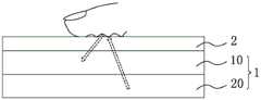
如图1所示,本发明第一实施例提供一种超声波指纹识别模组1,用于识别手指的指纹,所述超声波指纹识别模组1包括超声波发射层20和超声波接收层10,所述超声波发射层20用于发射超声波信号,发射的超声波信号经手指反射后由所述超声波接收层10接收,利用所述超声波接收层10所接收的超声波信号获取指纹信息。As shown in FIG. 1 , the first embodiment of the present invention provides an ultrasonic
其中超声波发射层20和超声波接收层10的位置可以互换,请参阅图2中所示。一般来说,在手指与超声波指纹识别模组1之间还设有触摸层2,该触摸层2可以是显示屏、玻璃、保护膜等,其为超声波指纹识别模组1提供保护,延长其使用寿命,当然在一些实施例中也可以省略。The positions of the
请一并参阅图3,所述超声波发射层20包括多个层叠设置且并联的压电薄膜201,其等效电路请参阅图4,每个压电薄膜201相当于一个电容。本发明所提供的超声波指纹识别模组1中,每个压电薄膜201均发出超声波从而使得声场强度叠加,从而使得当需要提供一定强度的超声波时,能降低对驱动电压的需求。故而能降低超声波指纹识别模组1的设计和制作难度,利于工业生产;而且,该超声波指纹识别模组1的耗电量较低,有效提高了实用性。Please refer to FIG. 3 , the
针对超声波发射层20,在该实施例中提供以下两种实施方式。For the ultrasonic
第一种实施方式first embodiment
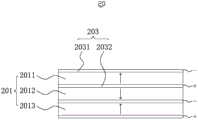
请参阅图3,所述超声波发射层20还包括用于向压电薄膜201施加驱动电压的多个电极203。在图3中以压电薄膜201设有三层为例,即所述压电薄膜201包括第一压电薄膜2011、第二压电薄膜2012及第三压电薄膜2013,在每个压电薄膜201两侧均设置电极203且两侧电极203 的电性相反;即所述电极203包括第一电极2031和第二电极2032,第一电极2031为负极,第二电极2032为正极。Referring to FIG. 3 , the
所述超声波发射层20的多个所述层叠设置的压电薄膜201中,相邻两个压电薄膜201的极化方向(图3中箭头所示)相反且共用设置于两者之间的电极203。可以理解,由于相邻两个压电薄膜201的极化方向相反,而两侧电极203所提供的电场方向亦相反,即能使得所发射超声波信号一致,从而能线性增强。Among the plurality of piezoelectric
第二种实施方式Second Embodiment
请参阅图5,第二种实施方式与第一种实施方式不同在于,每个压电薄膜201的极化方向(图5中箭头所示) 相同。也就是说,所述超声波发射层20的多个所述层叠设置的压电薄膜201的极化方向相同,且相邻两个压电薄膜201之间设置隔离层205,每个电极203仅作用于一个压电薄膜201。Referring to FIG. 5 , the second embodiment is different from the first embodiment in that the polarization directions (shown by arrows in FIG. 5 ) of each
在该实施方式中,每个压电薄膜201与两侧的电极 203构成一个单元,每个压电薄膜201所发射超声波信号一致,并通过隔离层205使单元之间电性隔绝,从而多个超声波信号叠加实现线性增强。In this embodiment, each
上述两种实施方式相比,第一种实施方式中,由于不需要设置隔离层205,因而厚度较低更能满足产品轻薄化的需求;第二种实施方式中,每个单元的结构与电性关系一致,更利于大规模生产。Compared with the above two embodiments, in the first embodiment, since the
在一些优选的实施例中,所述超声波发射层20的压电薄膜201的层数量为2-4。可以理解,随着层数量的增加,降低驱动电压的效果越好,但是其厚度也随之增加,因此当压电薄膜201的层数量为2-4时,既能有效的降低驱动电压,还能使得超声波发射层20的厚度较小。In some preferred embodiments, the number of layers of the piezoelectric
优选地,所述压电薄膜201是采用原位极化的方式极化形成。具体地,所述压电薄膜201包括相对的第一表面和第二表面,使该压电薄膜201的第一表面电势为零;在所述压电薄膜201的第二表面的上方提供第一电场及第二电场,第一电场的电势高于第二电场的电势;在第一电场的作用下电离所述压电薄膜201上方的环境气体,该环境气体穿过第二电场而聚集在压电薄膜201的第二表面,使所述压电薄膜201内形成沿薄膜厚度方向的膜内电场,对所述压电薄膜201进行极化形成所述压电薄膜201。Preferably, the
在实际生产中,可以是采用化学气相沉积、物理气相沉积、等离子体溅射等方式形成压电薄膜201。现有技术中,压电薄膜201通常是通过采购现有的成品通过一层粘结层粘附在基体上来进行极化,通常,此种方法形成的压电层厚度均在30μm以上,不适应现有电子器件轻薄的发展趋势,而且采用这种压电层的超声波指纹识别模组,由于压电层太厚,因此分辨率较低。而本发明提供的压电薄膜201采用原位形成的方式,因此厚度很薄,而且形成工艺简单,从而减小超声波信号的传输损耗,有利于提高超声波指纹识别模组1的指纹识别的分辨率。再者,本发明相较于直接在压电薄膜201的上下表面设置电极,不会使压电薄膜201直接承受所施加的高压电场,能避免压电薄膜201被击穿。本发明可采用等离子体极化(具体可参见申请号为201710108374.9的中国专利申请) 或X射线极化(具体可参见申请号为201611222575.3的中国专利申请)的方式形成所述压电薄膜201,所形成的压电薄膜201能够做到很薄,其厚度小于30μm,并可进一步为小于9μm。而且,本该压电薄膜201的压电效应较好以及使用寿命长,能够很好的适用在超声波指纹识别模组1中,利于实现超声波指纹识别模组1较好的识别效果。本发明中,进行了原位极化的所述压电薄膜201的压电效应D33的范围为20-35pC/N。In actual production, the piezoelectric
所述压电薄膜201的材料为压电材料,具体可选用但不限于:聚偏氟乙烯,聚氯乙烯,聚-γ-甲基-L-谷氨酸酯,聚碳酸酯、聚偏氟乙烯共聚物中的一种或者几种的组合。The material of the
在一些优选的实施例中,所述压电薄膜201的材料选用聚偏氟乙烯的共聚物为聚偏氟乙烯-三氟乙烯共聚物,为了获得压电效应较好的压电薄膜201,所述聚偏氟乙烯与三氟乙烯的质量比的范围是(60-95):(5-30),优选地,其质量比的范围是(75-86):(15-25),进一步优选地,其质量比为80:20,所述聚偏氟乙烯和三氟乙烯共聚物较单独选用聚偏氟乙烯可降低成本,且其还具有较好的压电效应。In some preferred embodiments, the material of the
本发明第二实施例提供一种电子设备,其包括第一实施例中所提供的超声波指纹识别模组,本发明所提供的电子设备,具有耗电量低的优点。The second embodiment of the present invention provides an electronic device, which includes the ultrasonic fingerprint identification module provided in the first embodiment. The electronic device provided by the present invention has the advantage of low power consumption.
与现有技术相比,本发明所提供的一种超声波指纹识别模组,超声波发射层包括多个层叠设置且并联的压电薄膜,每个压电薄膜均发出超声波从而使得声场强度叠加,从而使得当需要提供一定强度的超声波时,能降低对驱动电压的需求。故而能降低超声波指纹识别模组的设计和制作难度,利于工业生产;而且,该超声波指纹识别模组的耗电量较低,有效提高了实用性。Compared with the prior art, in an ultrasonic fingerprint identification module provided by the present invention, the ultrasonic emission layer includes a plurality of piezoelectric films arranged in layers and connected in parallel, and each piezoelectric film emits ultrasonic waves so that the sound field intensity is superimposed, thereby So that when a certain intensity of ultrasonic waves needs to be provided, the demand for driving voltage can be reduced. Therefore, the difficulty of designing and manufacturing the ultrasonic fingerprint identification module can be reduced, which is beneficial to industrial production; moreover, the power consumption of the ultrasonic fingerprint identification module is low, and the practicability is effectively improved.
进一步的是,所述超声波发射层还包括用于向压电薄膜施加驱动电压的多个电极;所述超声波发射层的多个所述层叠设置的压电薄膜的极化方向相同,且相邻两个压电薄膜之间设置隔离层,每个电极仅作用于一个压电薄膜。每个压电薄膜与两侧的电极构成一个单元,每个单元的结构与电性关系一致,更利于大规模生产。或者,所述超声波发射层还包括用于向压电薄膜施加驱动电压的多个电极;所述超声波发射层的多个所述层叠设置的压电薄膜中,相邻两个压电薄膜的极化方向相反且共用设置于两者之间的电极。由于不需要设置隔离层,因而厚度较低更能满足产品轻薄化的需求。Further, the ultrasonic emission layer further includes a plurality of electrodes for applying a driving voltage to the piezoelectric film; the polarization directions of the stacked piezoelectric films of the ultrasonic emission layer are the same and adjacent to each other. An isolation layer is arranged between the two piezoelectric films, and each electrode only acts on one piezoelectric film. Each piezoelectric film and the electrodes on both sides form a unit, and the structure of each unit is consistent with the electrical relationship, which is more conducive to mass production. Alternatively, the ultrasonic emission layer further includes a plurality of electrodes for applying a driving voltage to the piezoelectric film; among the plurality of piezoelectric films arranged in layers in the ultrasonic emission layer, the electrodes of two adjacent piezoelectric films The electrodes are in opposite directions and share the electrodes disposed therebetween. Since there is no need to set an isolation layer, the lower thickness can better meet the needs of light and thin products.
进一步的是,所述超声波发射层的压电薄膜的层数量为2-4。当压电薄膜201的层数量为2-4时,既能有效的降低驱动电压,还能使得超声波发射层的厚度较小。Further, the number of layers of the piezoelectric thin film of the ultrasonic emission layer is 2-4. When the number of layers of the piezoelectric
进一步的是,所述压电薄膜通过原位极化的方式形成。该压电薄膜具有厚度低质量好的优点。Further, the piezoelectric thin film is formed by in-situ polarization. The piezoelectric film has the advantages of low thickness and good quality.
进一步的是,所述压电薄膜的材料为聚偏氟乙烯、聚氯乙烯、聚-γ-甲基-L-谷氨酸酯、聚碳酸酯或者聚偏氟乙烯共聚物,具有较高的压电常数。所述压电薄膜的压电常数d33为20-35pC/N。Further, the material of the piezoelectric film is polyvinylidene fluoride, polyvinyl chloride, poly-γ-methyl-L-glutamate, polycarbonate or polyvinylidene fluoride copolymer, which has a high Piezoelectric constant. The piezoelectric constant d33 of the piezoelectric film is 20-35 pC/N.
进一步的是,所述压电薄膜的厚度小于30μm,能很好的符合产品轻薄化的需求。而且所述压电薄膜的厚度能进一步小于9μm。Further, the thickness of the piezoelectric film is less than 30 μm, which can well meet the requirements of light and thin products. Also, the thickness of the piezoelectric thin film can be further smaller than 9 μm.
本发明还提供一种电子设备,其包括上述的超声波指纹识别模组,具有耗电量低的优点。The present invention also provides an electronic device, which includes the above-mentioned ultrasonic fingerprint identification module, and has the advantage of low power consumption.
以上所述仅为本发明的较佳实施例而已,并不用以限制本发明,凡在本发明的原则之内所作的任何修改,等同替换和改进等均应包含本发明的保护范围之内。The above descriptions are only preferred embodiments of the present invention, and are not intended to limit the present invention. Any modifications, equivalent replacements and improvements made within the principles of the present invention should be included within the protection scope of the present invention.
Claims (8)
Translated fromChinesePriority Applications (1)
| Application Number | Priority Date | Filing Date | Title |
|---|---|---|---|
| CN201710665982.XACN107451572B (en) | 2017-08-07 | 2017-08-07 | Ultrasonic fingerprint recognition module and electronic equipment |
Applications Claiming Priority (1)
| Application Number | Priority Date | Filing Date | Title |
|---|---|---|---|
| CN201710665982.XACN107451572B (en) | 2017-08-07 | 2017-08-07 | Ultrasonic fingerprint recognition module and electronic equipment |
Publications (2)
| Publication Number | Publication Date |
|---|---|
| CN107451572A CN107451572A (en) | 2017-12-08 |
| CN107451572Btrue CN107451572B (en) | 2020-07-03 |
Family
ID=60490198
Family Applications (1)
| Application Number | Title | Priority Date | Filing Date |
|---|---|---|---|
| CN201710665982.XAActiveCN107451572B (en) | 2017-08-07 | 2017-08-07 | Ultrasonic fingerprint recognition module and electronic equipment |
Country Status (1)
| Country | Link |
|---|---|
| CN (1) | CN107451572B (en) |
Families Citing this family (9)
| Publication number | Priority date | Publication date | Assignee | Title |
|---|---|---|---|---|
| CN108389958B (en)* | 2018-01-24 | 2021-12-03 | 业成科技(成都)有限公司 | Ultrasonic vibration element and ultrasonic sensor |
| CN108073919B (en)* | 2018-02-28 | 2020-09-22 | 惠州Tcl移动通信有限公司 | Ultrasonic fingerprint acquisition precision control processing method, storage medium and mobile terminal |
| CN108647673A (en)* | 2018-07-10 | 2018-10-12 | 深圳市本地传感科技有限公司 | A kind of touch-control, fingerprint and the three-in-one identifying system of pressure and electronic equipment |
| CN110134188B (en)* | 2019-04-26 | 2021-02-23 | 武汉华星光电技术有限公司 | Self-sounding display device |
| CN110399852B (en)* | 2019-07-30 | 2021-07-20 | Oppo广东移动通信有限公司 | Ultrasonic module control method and related products |
| CN112507761B (en)* | 2019-09-16 | 2024-07-16 | 京东方科技集团股份有限公司 | A fingerprint recognition module and its driving method, and display device |
| CN115022778A (en)* | 2021-03-04 | 2022-09-06 | 北京小米移动软件有限公司 | Sound production module and electronic equipment |
| CN113343800B (en)* | 2021-05-25 | 2023-04-07 | 电子科技大学 | Fingerprint touch identification module, fingerprint touch identification method and electronic equipment |
| CN118591253A (en)* | 2023-03-01 | 2024-09-03 | 华为技术有限公司 | Ultrasonic sensor and working method thereof, and electronic device |
Citations (10)
| Publication number | Priority date | Publication date | Assignee | Title |
|---|---|---|---|---|
| CN1105678A (en)* | 1994-01-21 | 1995-07-26 | 中国科学院化学研究所 | Trapezoidal polysiloxane capable of displaying non-linear optical effect and liquid crystal property and functional film |
| CN1187045A (en)* | 1996-12-31 | 1998-07-08 | 中国科学院长春应用化学研究所 | Method for preparing poly meta fluoroethylene piezoelectric film |
| CN1829082A (en)* | 2005-03-04 | 2006-09-06 | 鸿富锦精密工业(深圳)有限公司 | Surface acoustic wave device and multi-frequency mobile phone |
| CN101936770A (en)* | 2010-08-27 | 2011-01-05 | 上海交通大学 | High Intensity Focused Ultrasound Sound Field Measurement System |
| CN102252967A (en)* | 2011-04-06 | 2011-11-23 | 天津大学 | Piezoelectric detection device based on LSAW (laser surface acoustic wave) locating of PVDF (Polyvinylidene Fluoride) piezoelectric thin film |
| CN102420582A (en)* | 2011-11-29 | 2012-04-18 | 浙江大学 | Structure of surface acoustic wave device based on flexible substrate and manufacturing method thereof |
| JP5647943B2 (en)* | 2011-05-02 | 2015-01-07 | 帝人株式会社 | Laminated film |
| CN104677399A (en)* | 2014-11-24 | 2015-06-03 | 麦克思智慧资本股份有限公司 | Ultrasonic sensor |
| CN105032749A (en)* | 2015-07-09 | 2015-11-11 | 深圳市理邦精密仪器股份有限公司 | Multi-layer lamination ultrasonic transducer and manufacturing method thereof |
| CN106848053A (en)* | 2016-04-20 | 2017-06-13 | 王开安 | Macromolecule membrane polarization device |
Family Cites Families (1)
| Publication number | Priority date | Publication date | Assignee | Title |
|---|---|---|---|---|
| US9437802B2 (en)* | 2013-08-21 | 2016-09-06 | Fujifilm Dimatix, Inc. | Multi-layered thin film piezoelectric devices and methods of making the same |
- 2017
- 2017-08-07CNCN201710665982.XApatent/CN107451572B/enactiveActive
Patent Citations (10)
| Publication number | Priority date | Publication date | Assignee | Title |
|---|---|---|---|---|
| CN1105678A (en)* | 1994-01-21 | 1995-07-26 | 中国科学院化学研究所 | Trapezoidal polysiloxane capable of displaying non-linear optical effect and liquid crystal property and functional film |
| CN1187045A (en)* | 1996-12-31 | 1998-07-08 | 中国科学院长春应用化学研究所 | Method for preparing poly meta fluoroethylene piezoelectric film |
| CN1829082A (en)* | 2005-03-04 | 2006-09-06 | 鸿富锦精密工业(深圳)有限公司 | Surface acoustic wave device and multi-frequency mobile phone |
| CN101936770A (en)* | 2010-08-27 | 2011-01-05 | 上海交通大学 | High Intensity Focused Ultrasound Sound Field Measurement System |
| CN102252967A (en)* | 2011-04-06 | 2011-11-23 | 天津大学 | Piezoelectric detection device based on LSAW (laser surface acoustic wave) locating of PVDF (Polyvinylidene Fluoride) piezoelectric thin film |
| JP5647943B2 (en)* | 2011-05-02 | 2015-01-07 | 帝人株式会社 | Laminated film |
| CN102420582A (en)* | 2011-11-29 | 2012-04-18 | 浙江大学 | Structure of surface acoustic wave device based on flexible substrate and manufacturing method thereof |
| CN104677399A (en)* | 2014-11-24 | 2015-06-03 | 麦克思智慧资本股份有限公司 | Ultrasonic sensor |
| CN105032749A (en)* | 2015-07-09 | 2015-11-11 | 深圳市理邦精密仪器股份有限公司 | Multi-layer lamination ultrasonic transducer and manufacturing method thereof |
| CN106848053A (en)* | 2016-04-20 | 2017-06-13 | 王开安 | Macromolecule membrane polarization device |
Also Published As
| Publication number | Publication date |
|---|---|
| CN107451572A (en) | 2017-12-08 |
Similar Documents
| Publication | Publication Date | Title |
|---|---|---|
| CN107451572B (en) | Ultrasonic fingerprint recognition module and electronic equipment | |
| CN107958199B (en) | Fingerprint detection module, display device and electronic equipment | |
| TWI668463B (en) | Ultrasonic sensing module, method for making same, and electronic device | |
| CN105447470B (en) | Electronic device | |
| KR101521681B1 (en) | Touch Panel | |
| CN110275577B (en) | Ultrasound module and display | |
| WO2020134150A1 (en) | Ultrasonic fingerprint recognition module and display panel | |
| CN102520539B (en) | Touch control display device | |
| CN109858313B (en) | Ultrasonic fingerprint identification modules, devices and electronic equipment | |
| CN110865490A (en) | Array substrate, display panel and display device | |
| TW201828007A (en) | Sonic Touch Device and Electronic Device Having Same | |
| CN107832665A (en) | Display module and electronic equipment | |
| CN108846318A (en) | Ultrasonic fingerprint identification device and preparation method thereof and the electronic device for applying it | |
| TWI621982B (en) | Fingerprint identification device, manufacturing method thereof and display device | |
| CN107832671A (en) | Display device and electronic equipment | |
| JP5255486B2 (en) | Display device with input function | |
| CN115877979A (en) | Touch display module and touch display device | |
| US20160087188A1 (en) | Sensing device | |
| WO2018205582A1 (en) | Touch display module, display device, and driving method therefor | |
| TWI764361B (en) | Touch recognition device, display device and manufacturing method thereof | |
| CN116027923A (en) | Touch display module and touch display device | |
| US11417139B2 (en) | Display device | |
| CN118302026A (en) | Ultrasonic sensor, electronic device, and method for manufacturing ultrasonic sensor | |
| CN207851836U (en) | Composite fingerprint identification module and electronic equipment | |
| CN111129063A (en) | A display panel, its driving method and display device |
Legal Events
| Date | Code | Title | Description |
|---|---|---|---|
| PB01 | Publication | ||
| PB01 | Publication | ||
| SE01 | Entry into force of request for substantive examination | ||
| SE01 | Entry into force of request for substantive examination | ||
| TA01 | Transfer of patent application right | ||
| TA01 | Transfer of patent application right | Effective date of registration:20190604 Address after:610000 Shunsheng Road, Zhengxing Street, Tianfu New District, Chengdu City, Sichuan Province Applicant after:CHENGDU YIDAO TECHNOLOGY PARTNERSHIP (L.P.) Address before:611731 No. 2103, Building No. 798, Tianfu First Street, Chengdu High-tech Zone, Chengdu, Sichuan Province Applicant before:Wu Lu | |
| GR01 | Patent grant | ||
| GR01 | Patent grant | ||
| TA01 | Transfer of patent application right | ||
| TA01 | Transfer of patent application right | Effective date of registration:20200623 Address after:No.88, Yingbin Avenue, Shouan Town, Pujiang County, Chengdu City, Sichuan Province Applicant after:Chengdu Dachao Technology Co.,Ltd. Address before:610000 Sichuan city of Chengdu province Tianfu Zheng Xing Shun Shing Street No. 172 Applicant before:CHENGDU YIDAO TECHNOLOGY PARTNERSHIP (L.P.) | |
| TR01 | Transfer of patent right | ||
| TR01 | Transfer of patent right | Effective date of registration:20250407 Address after:Room 102, 1st Floor, Building 1, No. 151 Tianxin Road, High tech Zone, Chengdu City, Sichuan Province 610000 Patentee after:Chengdu core technology Co.,Ltd. Country or region after:China Address before:611600 No.88 Yingbin Avenue, Shouan Town, Pujiang County, Chengdu City, Sichuan Province Patentee before:Chengdu Dachao Technology Co.,Ltd. Country or region before:China |