CN107430558B - semiconductor memory device - Google Patents
semiconductor memory deviceDownload PDFInfo
- Publication number
- CN107430558B CN107430558BCN201580077296.XACN201580077296ACN107430558BCN 107430558 BCN107430558 BCN 107430558BCN 201580077296 ACN201580077296 ACN 201580077296ACN 107430558 BCN107430558 BCN 107430558B
- Authority
- CN
- China
- Prior art keywords
- memory
- memory cell
- address
- error
- data
- Prior art date
- Legal status (The legal status is an assumption and is not a legal conclusion. Google has not performed a legal analysis and makes no representation as to the accuracy of the status listed.)
- Active
Links
Images


Classifications
- G—PHYSICS
- G06—COMPUTING OR CALCULATING; COUNTING
- G06F—ELECTRIC DIGITAL DATA PROCESSING
- G06F11/00—Error detection; Error correction; Monitoring
- G06F11/07—Responding to the occurrence of a fault, e.g. fault tolerance
- G06F11/08—Error detection or correction by redundancy in data representation, e.g. by using checking codes
- G06F11/10—Adding special bits or symbols to the coded information, e.g. parity check, casting out 9's or 11's
- G06F11/1008—Adding special bits or symbols to the coded information, e.g. parity check, casting out 9's or 11's in individual solid state devices
- G06F11/1048—Adding special bits or symbols to the coded information, e.g. parity check, casting out 9's or 11's in individual solid state devices using arrangements adapted for a specific error detection or correction feature
- G06F11/106—Correcting systematically all correctable errors, i.e. scrubbing
- G—PHYSICS
- G06—COMPUTING OR CALCULATING; COUNTING
- G06F—ELECTRIC DIGITAL DATA PROCESSING
- G06F11/00—Error detection; Error correction; Monitoring
- G06F11/30—Monitoring
- G06F11/3003—Monitoring arrangements specially adapted to the computing system or computing system component being monitored
- G06F11/3037—Monitoring arrangements specially adapted to the computing system or computing system component being monitored where the computing system component is a memory, e.g. virtual memory, cache
- G—PHYSICS
- G06—COMPUTING OR CALCULATING; COUNTING
- G06F—ELECTRIC DIGITAL DATA PROCESSING
- G06F11/00—Error detection; Error correction; Monitoring
- G06F11/07—Responding to the occurrence of a fault, e.g. fault tolerance
- G06F11/08—Error detection or correction by redundancy in data representation, e.g. by using checking codes
- G06F11/10—Adding special bits or symbols to the coded information, e.g. parity check, casting out 9's or 11's
- G06F11/1008—Adding special bits or symbols to the coded information, e.g. parity check, casting out 9's or 11's in individual solid state devices
- G06F11/1068—Adding special bits or symbols to the coded information, e.g. parity check, casting out 9's or 11's in individual solid state devices in sector programmable memories, e.g. flash disk
- G—PHYSICS
- G11—INFORMATION STORAGE
- G11C—STATIC STORES
- G11C17/00—Read-only memories programmable only once; Semi-permanent stores, e.g. manually-replaceable information cards
- G11C17/14—Read-only memories programmable only once; Semi-permanent stores, e.g. manually-replaceable information cards in which contents are determined by selectively establishing, breaking or modifying connecting links by permanently altering the state of coupling elements, e.g. PROM
- G11C17/16—Read-only memories programmable only once; Semi-permanent stores, e.g. manually-replaceable information cards in which contents are determined by selectively establishing, breaking or modifying connecting links by permanently altering the state of coupling elements, e.g. PROM using electrically-fusible links
- G—PHYSICS
- G11—INFORMATION STORAGE
- G11C—STATIC STORES
- G11C17/00—Read-only memories programmable only once; Semi-permanent stores, e.g. manually-replaceable information cards
- G11C17/14—Read-only memories programmable only once; Semi-permanent stores, e.g. manually-replaceable information cards in which contents are determined by selectively establishing, breaking or modifying connecting links by permanently altering the state of coupling elements, e.g. PROM
- G11C17/18—Auxiliary circuits, e.g. for writing into memory
- G—PHYSICS
- G11—INFORMATION STORAGE
- G11C—STATIC STORES
- G11C29/00—Checking stores for correct operation ; Subsequent repair; Testing stores during standby or offline operation
- G11C29/04—Detection or location of defective memory elements, e.g. cell constructio details, timing of test signals
- G11C29/08—Functional testing, e.g. testing during refresh, power-on self testing [POST] or distributed testing
- G11C29/12—Built-in arrangements for testing, e.g. built-in self testing [BIST] or interconnection details
- G11C29/38—Response verification devices
- G11C29/42—Response verification devices using error correcting codes [ECC] or parity check
- G—PHYSICS
- G11—INFORMATION STORAGE
- G11C—STATIC STORES
- G11C29/00—Checking stores for correct operation ; Subsequent repair; Testing stores during standby or offline operation
- G11C29/04—Detection or location of defective memory elements, e.g. cell constructio details, timing of test signals
- G11C29/08—Functional testing, e.g. testing during refresh, power-on self testing [POST] or distributed testing
- G11C29/12—Built-in arrangements for testing, e.g. built-in self testing [BIST] or interconnection details
- G11C29/44—Indication or identification of errors, e.g. for repair
- G11C29/4401—Indication or identification of errors, e.g. for repair for self repair
- G—PHYSICS
- G11—INFORMATION STORAGE
- G11C—STATIC STORES
- G11C29/00—Checking stores for correct operation ; Subsequent repair; Testing stores during standby or offline operation
- G11C29/52—Protection of memory contents; Detection of errors in memory contents
- G—PHYSICS
- G11—INFORMATION STORAGE
- G11C—STATIC STORES
- G11C29/00—Checking stores for correct operation ; Subsequent repair; Testing stores during standby or offline operation
- G11C29/70—Masking faults in memories by using spares or by reconfiguring
- G11C29/78—Masking faults in memories by using spares or by reconfiguring using programmable devices
- G11C29/785—Masking faults in memories by using spares or by reconfiguring using programmable devices with redundancy programming schemes
- G—PHYSICS
- G06—COMPUTING OR CALCULATING; COUNTING
- G06F—ELECTRIC DIGITAL DATA PROCESSING
- G06F2201/00—Indexing scheme relating to error detection, to error correction, and to monitoring
- G06F2201/81—Threshold
- G—PHYSICS
- G06—COMPUTING OR CALCULATING; COUNTING
- G06F—ELECTRIC DIGITAL DATA PROCESSING
- G06F2201/00—Indexing scheme relating to error detection, to error correction, and to monitoring
- G06F2201/88—Monitoring involving counting
- G—PHYSICS
- G11—INFORMATION STORAGE
- G11C—STATIC STORES
- G11C29/00—Checking stores for correct operation ; Subsequent repair; Testing stores during standby or offline operation
- G11C29/04—Detection or location of defective memory elements, e.g. cell constructio details, timing of test signals
- G11C2029/0409—Online test
- G—PHYSICS
- G11—INFORMATION STORAGE
- G11C—STATIC STORES
- G11C29/00—Checking stores for correct operation ; Subsequent repair; Testing stores during standby or offline operation
- G11C29/04—Detection or location of defective memory elements, e.g. cell constructio details, timing of test signals
- G11C2029/0411—Online error correction
- G—PHYSICS
- G11—INFORMATION STORAGE
- G11C—STATIC STORES
- G11C29/00—Checking stores for correct operation ; Subsequent repair; Testing stores during standby or offline operation
- G11C29/04—Detection or location of defective memory elements, e.g. cell constructio details, timing of test signals
- G11C29/08—Functional testing, e.g. testing during refresh, power-on self testing [POST] or distributed testing
- G11C29/12—Built-in arrangements for testing, e.g. built-in self testing [BIST] or interconnection details
- G11C2029/4402—Internal storage of test result, quality data, chip identification, repair information
Landscapes
- Engineering & Computer Science (AREA)
- Theoretical Computer Science (AREA)
- Physics & Mathematics (AREA)
- Quality & Reliability (AREA)
- General Engineering & Computer Science (AREA)
- General Physics & Mathematics (AREA)
- Computing Systems (AREA)
- Mathematical Physics (AREA)
- For Increasing The Reliability Of Semiconductor Memories (AREA)
Abstract
Description
Translated fromChinese相关申请的交叉引用CROSS-REFERENCE TO RELATED APPLICATIONS
本申请案是基于2015年3月9日申请的第62/130,490号先前美国临时申请案且要求所述案的优先权权益,所述案的全部内容以引用的方式并入本文中。This application is based on, and claims the benefit of, prior US Provisional Application No. 62/130,490, filed March 9, 2015, the entire contents of which are incorporated herein by reference.
技术领域technical field
本发明实施例涉及一种半导体存储装置。Embodiments of the present invention relate to a semiconductor memory device.
背景技术Background technique
磁阻性随机存取存储器(MRAM)是其中用于存储信息的存储器单元采用具有磁阻效应的磁性元件的存储器装置。所述MRAM作为以高速操作、大存储容量及非易失性为特征的下一代存储器装置而受到关注。在此期间,正进行研究及开发以用MRAM取代动态随机存取存储器(DRAM)及静态随机存取存储器(SRAM)。为降低开发成本及实现容易取代,MRAM应可期望按与DRAM及SRAM相同的规范操作。Magnetoresistive random access memory (MRAM) is a memory device in which memory cells for storing information employ magnetic elements having a magnetoresistive effect. The MRAM has drawn attention as a next-generation memory device characterized by high-speed operation, large storage capacity, and non-volatility. During this period, research and development are underway to replace dynamic random access memory (DRAM) and static random access memory (SRAM) with MRAM. To reduce development costs and enable easy replacement, MRAM should be expected to operate to the same specifications as DRAM and SRAM.
附图说明Description of drawings
图1是展示根据实施例的存储器系统的示范性配置的框图。1 is a block diagram showing an exemplary configuration of a memory system according to an embodiment.
图2是展示所述实施例的存储器系统的存储器单元阵列的示范性配置的电路图。2 is a circuit diagram showing an exemplary configuration of a memory cell array of the memory system of the embodiment.
图3说明所述实施例的存储器系统的存储器单元的基本配置。FIG. 3 illustrates the basic configuration of the memory cells of the memory system of the embodiment.
图4是说明所述实施例的存储器系统的状态图。FIG. 4 is a state diagram illustrating the memory system of the embodiment.
图5是说明所述实施例的存储器系统的清除操作的流程图。FIG. 5 is a flowchart illustrating a clear operation of the memory system of the embodiment.
图6是说明所述实施例的存储器系统的清除操作的波形图。FIG. 6 is a waveform diagram illustrating a clear operation of the memory system of the embodiment.
图7是说明所述实施例的存储器系统的清除操作的波形图。FIG. 7 is a waveform diagram illustrating a clear operation of the memory system of the embodiment.
具体实施方式Detailed ways
一般来说,根据一个实施例,存储器系统包含:In general, according to one embodiment, a memory system includes:
第一存储器单元区域,其中提供第一存储器单元;a first memory cell region in which the first memory cells are provided;
第二存储器单元区域,其中提供第二存储器单元;a second memory cell region in which second memory cells are provided;
ECC电路,其校正通过所述第一存储器单元存储的数据的错误;以及an ECC circuit that corrects errors in data stored by the first memory cell; and
控制电路,如果成功校正所述第一存储器单元中的错误的次数达到第一值,那么所述控制电路用所述第二存储器单元取代所述第一存储器单元。A control circuit that replaces the first memory cell with the second memory cell if the number of successful corrections of errors in the first memory cell reaches a first value.
现将给出实施例的描述。在下文描述中,具有基本上相同功能及配置的结构元件将通过相同参考符号表示且仅在需要时给出重复描述。下文描述的实施例中的每一个仅展示实施所述实施例的技术理念的示范性设备及方法。所述实施例的技术理念并不限于下文描述的元件材料、形状、结构、布置等。所述实施例的技术理念可在权利要求书中定义的范围内改变。A description of the embodiments will now be given. In the following description, structural elements that have substantially the same function and configuration will be denoted by the same reference symbols, and repeated description will be given only when necessary. Each of the embodiments described below merely shows an exemplary apparatus and method for implementing the technical idea of the embodiment. The technical idea of the embodiment is not limited to the element material, shape, structure, arrangement, etc. described below. The technical idea of the embodiments can be changed within the scope defined in the claims.
功能块中的每一个可以硬件、计算机软件或其组合的形式实施。为阐明所述功能块具体所指,下文将在其功能方面对所述块进行解释。所述功能是实施为硬件还是软件是特定实施方案的问题或取决于对整个系统施加的设计限制。所属领域技术人员可针对实施例中的每一个以各种方式实施所述功能且如何实施所述功能是在实施例的范围内。Each of the functional blocks can be implemented in hardware, computer software, or a combination thereof. In order to clarify what the functional blocks specifically refer to, the blocks are explained below in terms of their functions. Whether the functionality is implemented as hardware or software is a matter of the particular implementation or depends on design constraints imposed on the overall system. Those skilled in the art may implement the described functions in various ways for each of the embodiments and it is within the scope of the embodiments how to implement the described functions.
(实施例)(Example)
<1>配置<1> Configuration
将参考其中将MRAM应用于存储器单元阵列的情况描述本发明实施例。Embodiments of the present invention will be described with reference to a case in which MRAM is applied to a memory cell array.
<1-1>存储器系统的配置<1-1> Configuration of the memory system
将参考图1给出根据实施例的存储器系统的基本配置的示意性描述。所述存储器系统1包括存储器控制器100及存储器装置200。A schematic description will be given of the basic configuration of the memory system according to the embodiment with reference to FIG. 1 . The
<1-2>存储器控制器的配置<1-2> Configuration of the memory controller
所述实施例的存储器控制器100从主机2接收命令。根据所述命令,存储器控制器100从存储器装置200读取数据且将数据写入于所述存储器装置200中。The
存储器控制器100具有主机接口(主机I/F)110、数据缓冲器120、状态寄存器130、中央处理单元(CPU)140、装置接口(I/F)150、错误校正码(ECC)电路160、熔丝控制器170及地址计数器180。The
所述主机接口110连接到主机(外部设备)2(例如,个人计算机)且进一步连接到存储器控制器100的总线190。通过主机接口110在主机2与存储器系统1之间发射及接收数据。The
所述数据缓冲器120连接到主机接口110且进一步连接到总线190。数据缓冲器120通过主机接口110接收从主机2发射到存储器系统1的数据且暂时存储所述数据。而且,数据缓冲器120暂时存储待通过主机接口110从存储器系统1发射到主机2的数据。数据缓冲器120可为易失性存储器或非易失性存储器。The
CPU 140控制存储器系统1的整体操作。例如,CPU 140根据从主机2接收的命令对存储器装置200执行预定处理。The
状态寄存器130是(例如)易失性存储器且存储设定信息、通过CPU 140执行的命令及状态信号。状态寄存器130可为易失性存储器或非易失性存储器。The
装置接口150介接存储器控制器100与存储器装置200且启用将在所述存储器控制器100与所述存储器装置200之间发射及接收的各种信号。装置接口150连接到ECC电路160、地址计数器180及总线190。The
ECC电路160通过数据缓冲器120接收从主机2接收的写入数据。ECC电路160将错误校正码添加到所述写入数据。ECC电路160将所述写入数据(包含添加到所述写入数据的错误校正码)供应到数据缓冲器120或装置接口150。The ECC circuit 160 receives the write data received from the
ECC电路160通过装置接口150接收从存储器装置200供应的数据。所述数据是存储于存储器单元阵列210的存储器单元群组中的数据。所述存储器单元群组是一组存储器单元MC且在读取操作时对应于读取单元。ECC电路160确定从存储器装置200接收的数据是否含有错误。如果所述所接收数据含有错误,那么ECC电路使用错误校正码对所述所接收数据执行错误校正。ECC电路160将经受错误校正的数据供应到数据缓冲器120、装置接口150等。如果确定从存储器装置200读取的数据含有错误,那么ECC电路160将错误通知信号“Error”供应到熔丝控制器170。如果确定从存储器装置200读取的数据不含有错误,那么ECC电路160将通知信号“No_Error”供应到主机2。The ECC circuit 160 receives data supplied from the
熔丝控制器170根据错误出现的次数(在本发明实施例中,所述次数等于通过ECC电路160成功校正错误的次数)产生冗余地址信息(通过所述冗余地址信息,用冗余单元取代用于存储数据的存储器单元)及熔丝编程电压产生信号。The
熔丝控制器170包括失效地址寄存器170a、地址比较器170b、失效计数寄存器170c、熔丝地址产生器170d及熔丝编程电压产生器170e。The
所述失效地址产生器170a存储表示其中通过ECC电路160检测错误的存储器单元阵列210的地址信息作为失效地址信息。为简洁起见,存储器单元阵列210的地址在本发明实施例的描述中可简称为“地址”。“地址”是表示存储器单元阵列210或存储器单元群组的存储器单元MC所处的位置的信息。失效地址寄存器170a可存储缺陷地址信息的多个片段。失效地址寄存器170a可为易失性存储器或非易失性存储器。The
地址比较器170b比较ECC电路160确定为含有错误的地址与存储于失效地址寄存器170a中的地址。更特定地说,如果地址比较器170b从ECC电路160接收错误通知信号“Error”,那么其从地址计数器180接收表示错误的位置的地址。随后,地址比较器170b确定所述所接收地址信息是否存储于失效地址寄存器170a中。Address comparator 170b compares the address determined by ECC circuit 160 to contain an error with the address stored in
失效计数寄存器170c存储表示错误在存储于失效地址寄存器170a中的缺陷地址处出现的次数(所述次数等于成功校正所述错误的次数)的数据。在通过ECC电路160检测到错误之后,失效计数寄存器170c增加错误在对应于所述错误的地址处重复的次数。当错误出现的次数(成功校正所述错误的次数)增加且达到存储于失效计数寄存器170c中的阈值时,所述失效计数寄存器170c将信号“Err_max”发射到熔丝地址产生器170d及熔丝编程电压产生器170e。失效计数寄存器170c可为易失性存储器或非易失性存储器。The
如果错误在缺陷地址处出现的次数(即,成功校正所述错误的次数)达到阈值,那么熔丝地址产生器170d产生冗余地址信息,通过所述冗余地址信息,用冗余单元取代对应于缺陷地址的存储器单元MC。更特定地说,在从失效计数寄存器170c接收到信号“Err_max”之后,熔丝地址寄存器170d产生列熔丝212及/或行熔丝214的熔丝地址(冗余地址信息),使得用冗余单元的地址取代对应地址。熔丝地址产生器170d可经配置以依使得用冗余单元群组取代存储器单元群组或用冗余单元取代单一存储器单元的方式产生一或多个熔丝地址。结合本发明实施例,参考其中存储器系统1用冗余单元取代存储器单元的情况。If the number of times an error occurs at a defective address (ie, the number of times the error is successfully corrected) reaches a threshold, the
如果确定错误在缺陷地址处出现的次数已达到阈值,那么熔丝编程电压产生器170e产生熔丝编程电压产生信号。在接收到所述熔丝编程电压产生信号之后,存储器装置200的内部电压产生器260产生电压,在所述电压下对列熔丝212及/或行熔丝214执行熔丝编程操作。The fuse
熔丝控制器170可包括控制失效地址寄存器170a、地址比较器170b、失效计数寄存器170c、熔丝地址产生器170d及熔丝编程电压产生器170e的控制器。
地址计数器180存储用于稍后提及的清除操作的地址信息。The
<1-3>存储器装置的配置<1-3> Configuration of memory device
所述实施例的存储器装置200包括存储器单元阵列(其可简称为“单元阵列”)210、感测放大器/写入驱动器211、列熔丝212、行解码器213、行熔丝214、阵列控制器215、DQ电路230、控制器240、命令/地址电路250及间隔电压产生器260。The
所述存储器单元阵列210是包括布置成二维矩阵图案的多个存储器单元的MRAM。存储器单元阵列210包括普通单元阵列(其还可被称为普通存储器区域)210a及冗余单元阵列(其还可被称为冗余存储器区域)210b。所述普通单元阵列210a及所述冗余单元阵列210b中的每一个包含多个存储器单元MC。所述普通单元阵列210a及所述冗余单元阵列210b在存储器单元MC的结构方面相同。普通单元阵列210a是用于正常读取操作或正常写入操作的基本存储器区域。冗余单元阵列210b是用于补救普通单元阵列210a的缺陷的存储器区域。例如,假设普通单元阵列210a具有固有缺陷且此缺陷是在装运之前执行的存储器系统1的测试操作中发现。在此情况下,用冗余单元阵列210b的存储器单元取代其中出现错误的存储器单元MC。通过此取代,防止使用固有缺陷存储器单元MC。如稍后将描述,可在装运存储器系统1之后执行的清除操作中执行对缺陷存储器单元的取代。在对应于待存取的地址的冗余信息存储于列熔丝212及/或行熔丝214中的情况下,存取冗余单元阵列210b。在对应于待存取的地址的冗余信息未存储于列熔丝212或行熔丝214中的情况下,存取普通单元阵列210a。在说明书中,提供于普通单元阵列210a中的存储器单元MC还被称为普通单元且提供于冗余单元阵列210b中的存储器单元还被称为冗余单元阵列。稍后将描述存储器单元阵列210的特定配置。The
感测放大器/写入驱动器(其还被称为位线控制器)211经布置以在存储器单元阵列210的位线方向上延伸。所述感测放大器/写入驱动器211包含感测放大器及写入驱动器。所述感测放大器连接到位线BL且在其检测到流动通过连接到选定字线WL的存储器单元MC的电流时从所述存储器单元MC读取数据。所述写入驱动器连接到位线BL且在其将电流供应到连接到选定字线WL的存储器单元MC时将数据写入于所述存储器单元MC中。感测/写入驱动器211基于从阵列控制器215供应的控制信号来控制位线BL及源极线SL。通过数据总线220及DQ电路230执行感测放大器/写入驱动器211与外部输入/输出终端(还被称为数据线)DQ(未展示)之间的数据交换。A sense amplifier/write driver (which is also referred to as a bit line controller) 211 is arranged to extend in the bit line direction of the
列熔丝212是电可编程非易失性存储器(例如,反熔丝或电熔丝)且存储存储器单元阵列210上的列冗余信息。所述列熔丝212将(例如)所述列冗余信息供应到阵列控制器215及感测放大器/写入驱动器211。当列熔丝212将列冗余信息供应到阵列控制器215时,所述阵列控制器215存取对应冗余单元。所述列冗余信息包含位线对信息(即,位线及源极线上的信息)、列信息等。如果在下文描述的方法中,缺陷存储器单元是在装运之前的测试中发现,那么将列冗余信息存储于列熔丝212中。Column fuses 212 are electrically programmable non-volatile memory (eg, antifuses or electrical fuses) and store column redundancy information on the
行解码器213经布置以在存储器单元阵列210的字线方向上延伸且连接到存储器单元阵列210的字线。所述行解码器213解码从命令/地址电路250供应的命令地址信号CAi的地址且基于字线选择信号选择字线。The
行熔丝214是电可编程非易失性存储器(例如,反熔丝或电熔丝)且存储存储器单元阵列210上的行冗余信息。所述行熔丝214将所述行冗余信息供应到行解码器213。当行熔丝214将行冗余信息供应到行解码器213时,所述行解码器213存取对应冗余单元。所述行冗余信息包含字线信息、行信息等。如果在下文描述的方法中,缺陷存储器单元是在装运之前的测试中发现,那么将行冗余信息存储于行熔丝214中。Row fuses 214 are electrically programmable non-volatile memory (eg, antifuses or electrical fuses) and store row redundancy information on the
列熔丝212及行熔丝214可提供为单一熔丝(存储区域)。如果列冗余信息及行冗余信息无需彼此区别,那么将其简称为冗余信息。The column fuses 212 and the row fuses 214 may be provided as a single fuse (storage area). If the column redundant information and the row redundant information do not need to be distinguished from each other, they are simply referred to as redundant information.
阵列控制器215用作列解码器且控制位线BL及源极线SL。The
DQ电路230通过外部输入/输出终端DQ(还被称为数据线)(未展示)使数据能够在存储器控制器100与存储器装置200之间交换。
控制器240接收通过存储器控制器100的装置接口150供应的各种外部控制信号(例如,芯片选择信号CS、时钟信号CK、时钟启用信号CKE等)。所述控制器240控制命令地址电路250且使地址与命令彼此区别。控制器240执行存储器装置200的整体控制且控制稍后描述的对存储器单元阵列210的存取。The
命令地址电路250通过存储器控制器100的装置接口150接收供应到所述命令地址电路250的命令地址信号CAi。命令地址电路250将命令地址信号DCAi传送到行解码器213及阵列控制器215。The command address circuit 250 receives the command address signal CAi supplied to the command address circuit 250 through the
内部电压产生器260产生存储器装置200的每一操作所需的内部电压(例如,高于电源电压的升压电压)。受控制器240控制,所述内部电压产生器260执行电压升压操作且产生所需电压。在接收到熔丝编程电压产生信号之后,内部电压产生器260产生可将冗余信息写入列熔丝212及行熔丝214中的电压。The internal voltage generator 260 generates an internal voltage (eg, a boost voltage higher than the power supply voltage) required for each operation of the
<1-4>存储器单元阵列<1-4> Memory cell array
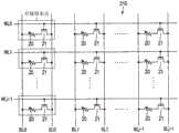
将参考图2给出根据实施例的存储器单元阵列的配置的描述。如上文所描述,存储器单元阵列210包括布置成二维矩阵图案的多个存储器单元。在行方向上延伸的字线WL及在列方向上延伸的位线BL彼此交叉。邻近的两条位线BL形成一对,且存储器单元MC是提供于字线WL与位线对(在本发明实施例中,为描述目的将所述位线对称为位线BL及源极线SL)之间的交叉点处。更明确地说,存储器单元阵列210包括多条字线WL0到WLi-1、多条位线BL0到BLj-1及多条源极线SL0到SLj-1。存储器单元阵列的行中的一个连接到一条字线WL且存储器单元阵列的列中的一个连接到通过一条位线BL及一条源极线SL形成的一对。A description will be given of the configuration of the memory cell array according to the embodiment with reference to FIG. 2 . As described above, the
每一存储器单元MC包含磁性穿隧结(MTJ)元件20及选择晶体管21。所述选择晶体管21是由(例如)N通道MOSFET形成。Each memory cell MC includes a magnetic tunnel junction (MTJ)
所述MTJ元件20的一端连接到位线BL且其另一端连接到选择晶体管21的漏极。所述选择晶体管21的栅极连接到字线WL且其源极连接到源极线SL。One end of the
普通单元阵列210a及冗余单元阵列210b具有如上所述的基本上相同的基本配置,但未提及其间的差异。The
<1-5>存储器单元<1-5> Memory unit
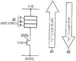
将参考图3给出根据实施例的存储器单元的配置的示意性描述。A schematic description of the configuration of the memory cell according to the embodiment will be given with reference to FIG. 3 .
如图3中所展示,所述实施例的存储器单元MC的MTJ元件20的一端连接到位线BL且所述MTJ元件20的另一端连接到单元晶体管21的电流路径中的一个。单元晶体管21的另一端连接到源极线SL。利用穿隧磁阻(TMR)效应的MTJ元件20具有堆栈结构,所述堆栈结构包括两个铁磁性层F及P以及夹置于所述铁磁性层F与P之间的一个非磁性层(穿隧绝缘膜)B。MTJ元件通过利用由自旋极化穿隧效应引起的磁阻的变动来存储数字数据。可根据两个铁磁性层F及P的磁性定向将MTJ元件20设定为低电阻状态或高电阻状态。例如,如果低电阻状态是定义为数据“0”且高电阻状态是定义为数据“1”,那么可将1-位数据记录于MTJ元件20中。毋庸置疑,所述低电阻状态可定义为数据“1”且所述高电阻状态可定义为数据“0”。As shown in FIG. 3 , one end of the
例如,通过按所提及顺序堆栈固定层(钉扎层)P、穿隧势垒层B及记录层(自由层)F来形成MTJ元件。所述钉扎层P及所述自由层F是由铁磁性材料制成且所述穿隧势垒层B是绝缘膜(例如,Al2O3或MgO)。钉扎层P是其中磁性定向固定的层,而自由层F是其中磁性定向可变且利用磁性定向存储数据的层。For example, an MTJ element is formed by stacking a pinned layer (pinning layer) P, a tunneling barrier layer B, and a recording layer (free layer) F in the mentioned order. The pinning layer P and the free layer F are made of a ferromagnetic material and the tunneling barrier layer B is an insulating film (eg, Al2 O3 or MgO). The pinned layer P is a layer in which the magnetic orientation is fixed, and the free layer F is a layer in which the magnetic orientation is variable and data is stored using the magnetic orientation.
当电流在写入操作中沿着箭头A1的方向流动时,自由层F的磁性定向变为相对于钉扎层P的磁性定向反平行(AP状态)。因此,产生高电阻状态(数据“1”)。当电流在写入操作中沿着箭头A2的方向流动时,自由层F的磁性定向变为相对于钉扎层P的磁性定向平行(P状态)。因此,产生低电阻状态(数据“0”)。如可见,可通过改变电流流动的方向来将不同数据写入MTJ元件中。When current flows in the direction of arrow A1 in the write operation, the magnetic orientation of the free layer F becomes antiparallel with respect to the magnetic orientation of the pinned layer P (AP state). Therefore, a high resistance state (data "1") is generated. When the current flows in the direction of arrow A2 in the write operation, the magnetic orientation of the free layer F becomes parallel with respect to the magnetic orientation of the pinned layer P (P state). Therefore, a low resistance state (data "0") is produced. As can be seen, different data can be written into the MTJ element by changing the direction of current flow.
<2>操作<2> Operation
<2-1>状态转变<2-1> State transition
将参考图4给出根据实施例的存储器系统的状态转变的描述。在图4中,细箭头指示在从主机2接收命令时MRAM的状态如何转变。在图4中,粗箭头指示在预定操作结束时在未从主机2接收任何命令的情况下MRAM的状态如何自动转变。A description will be given of state transitions of the memory system according to the embodiment with reference to FIG. 4 . In FIG. 4 , thin arrows indicate how the state of the MRAM transitions when a command is received from the
[状态1]电源开启[Status 1] Power on
如图4中所展示,在将电力从主机2供应到存储器系统1时,所述存储器系统1转变到电源开启状态(状态1)。As shown in FIG. 4, when power is supplied from the
[状态2]复位[state 2] reset
当将复位命令从主机2供应到存储器系统1时,所述存储器系统1转变到复位状态(状态2)。当存储器系统1处于电源开启状态中及/或处于闲置状态中时,主机2可将所述复位命令供应到此存储器系统。When a reset command is supplied from the
[状态3]闲置[State 3] Idle
在复位处理之后,清除操作或预启动操作结束,存储器系统1自动转变到闲置状态(状态3)。在所述闲置状态中,存储器系统1准备启动(开启状态)。After the reset process, the clear operation or the pre-boot operation ends, and the
[状态4]清除[state 4] clear
当将清除命令从主机2供应到存储器系统1时,所述存储器系统1转变到清除状态(状态4)。当存储器系统1处于闲置状态(状态3)中时,主机2可将所述清除命令供应到此存储器系统。清除操作的细节将稍后予以描述。When a clear command is supplied from the
[状态5]作用中[Status 5] Active
当将启动命令从主机2供应到存储器系统1时,所述存储器系统1转变到作用中状态(状态5)。当存储器系统1处于闲置状态(状态3)中时,主机2可将所述启动命令供应到此存储器系统。当读取/写入操作或模式寄存器读取/写入操作结束时,存储器系统自动转变到所述作用中状态(状态5)。When a start command is supplied from the
[状态6]读取/写入[state 6] read/write
当将读取/写入命令(RD/WR)从主机2供应到存储器系统1时,所述存储器系统1转变到读取/写入状态(状态6)。当存储器系统1处于作用中状态(状态5)中及/或处于所述读取/写入状态(状态6)中时,主机2可将所述读取/写入命令供应到此存储器系统。When a read/write command (RD/WR) is supplied from the
[状态7]模式寄存器读取/写入[Status 7] Mode Register Read/Write
当将模式寄存器读取/写入命令(MRR/MRW)从主机2供应到存储器系统1时,所述存储器系统1转变到模式寄存器读取/写入状态(状态7)。当存储器系统1处于作用中状态(状态5)中时,主机2可将所述模式寄存器读取/写入命令供应到此存储器系统。When the mode register read/write command (MRR/MRW) is supplied from the
“模式寄存器读取”是从状态寄存器130读取数据。“模式寄存器写入”是将数据写入状态寄存器130中。状态寄存器130存储表示存储器装置200的操作状态等的数据。例如,状态寄存器130存储表示脉冲串的种类、所述脉冲串的长度、延时周期等的数据。A "mode register read" is to read data from the
[状态8]预启动[Status 8] Preboot
当将预作用命令从主机2供应到存储器系统1时,所述存储器系统1转变到预启动状态(状态8)。当存储器系统1处于作用中状态(状态5)中及/或处于闲置状态(状态3)中时,主机2可将所述预作用命令供应到此存储器系统。When a pre-action command is supplied from the
图4中所展示的状态转变图是实例且可以不同方式执行状态转变。例如,当除DDRx系统或LPDDRx系统以外的系统处于闲置状态中时,可将清除命令供应到所述系统,且可响应于所述清除命令执行清除操作。The state transition diagram shown in FIG. 4 is an example and the state transitions may be performed in different ways. For example, when a system other than a DDRx system or an LPDDRx system is in an idle state, a clear command may be supplied to the system, and a clear operation may be performed in response to the clear command.
<2-2>清除操作<2-2> Clear operation
将参考图5给出根据实施例的存储器系统的清除操作的描述。A description will be given of a clear operation of the memory system according to the embodiment with reference to FIG. 5 .
清除操作是在用户不执行普通读取/写入操作时存储器控制器100执行的操作。通过清除操作,周期性地检查普通单元阵列210a的存储器单元MC且校正数据错误。The clear operation is an operation performed by the
在清除操作中,如果存储器控制器100检测到在存储于预定存储器单元MC中的数据中出现的错误,那么所述存储器控制器100校正所述错误且将经校正数据存储于所述存储器单元MC中。如在上文阐述的<1-5>中所描述,在将数据写入存储器单元MC中时,将电流供应到MTJ元件20。因此,MTJ元件20可根据执行写入操作的次数的增加而随着时间劣化。例如,多次经历错误的存储器单元MC(其经历成功错误校正达相同次数)极有可能是随着时间变得有缺陷的单元。即使将校正数据写回到此存储器单元MC中,所述校正数据也无法正确写入。因此,如果将经历错误超过阈值的存储器单元MC(其经历成功错误校正达相同次数)视为次要缺陷单元。应期望用冗余单元MC取代此存储器单元MC。因此,可用冗余单元MC取代随着时间变得有缺陷的单元。In the clear operation, if the
将更特定描述上文提及的清除操作。The above-mentioned clearing operation will be described more specifically.
当存储器系统1处于闲置状态中时,主机2可发出清除命令到此存储器系统。在从主机2接收到所述清除命令之后,存储器系统1开始清除操作。When the
[步骤S1001][Step S1001]
在接收到清除命令之后,装置接口150从地址计数器180读取存储器单元阵列210的地址n。After receiving the clear command, the
[步骤S1002][Step S1002]
装置接口150发出地址n及读取命令到存储器装置200。所述存储器装置200基于所述所接收地址n及所述读取命令从存储器单元的地址n读取数据。接着,存储器装置200通过数据总线220、DQ电路230及数据线DQ(未展示)将读取数据d供应到存储器控制器100。因此,装置接口150通过数据线DQ接收数据d。
[步骤S1003][Step S1003]
装置接口150将数据d供应到ECC电路160以用于数据d的错误检测。ECC电路160确定所述所接收数据d是否含有错误。如果在数据d中检测到错误,那么ECC电路160使用错误校正码对数据d执行错误校正。The
[步骤S1004][Step S1004]
如果确定数据d含有错误(在步骤S1003中为是),那么ECC电路160将错误通知信号“Error”供应到熔丝控制器170。如果地址比较器170b从ECC电路160接收错误通知信号“Error”,那么所述地址比较器170b从地址计数器180接收地址n。If it is determined that the datad contains an error (YES in step S1003 ), the ECC circuit 160 supplies an error notification signal “Error” to the
随后,地址比较器170b确定地址n是否存储于失效地址寄存器170a中。换句话来说,地址比较器170b确定失效地址寄存器170a是否存储与对应于错误的地址信息(地址n)相同的地址信息。Subsequently, the address comparator 170b determines whether the addressn is stored in the
[步骤S1005][Step S1005]
如果地址比较器170b确定地址n未存储于失效地址寄存器170a中(在步骤S1004中为否),那么所述地址比较器170b将关于对应于错误的地址n的信息存储于失效地址寄存器170a中。If the address comparator 170b determines that the addressn is not stored in the
[步骤S1006][Step S1006]
如果地址比较器170b确定地址n存储于失效地址寄存器170a中(在步骤S1004中为是),那么失效计数寄存器170c使对应于地址n的计数M增加1(计数M:错误出现的次数或成功校正所述错误的次数)。If the address comparator 170b determines that the addressn is stored in the
如果失效地址寄存器170a存储新地址n,那么对应计数M是1(M=1)。If the
[步骤S1007][Step S1007]
失效计数寄存器170c确定对应于地址n的计数M是否已达到阈值Mmax。可以任何期望方式确定此阈值Mmax。所述阈值Mmax是存储于(例如)失效计数寄存器170c中。The
[步骤S1008][Step S1008]
如果错误出现的次数(成功校正所述错误的次数)已达到阈值Mmax,那么将对应于地址n的存储器单元MC视为已随着时间劣化且不能够存储准确数据。因此期望不应使用此存储器单元且应代替性地使用冗余单元阵列210b的存储器单元MC。将有关这一点给出更特定描述。If the number of occurrences of errors (the number of times the errors were successfully corrected) has reached a threshold value Mmax, then the memory cell MC corresponding to addressn is considered to have degraded over time and cannot store accurate data. It is therefore expected that this memory cell should not be used and that memory cell MC of
如果失效计数寄存器170c确定对应于地址n的计数M已达到阈值Mmax(在步骤S1007中为是),那么所述失效计数寄存器170c将信号“Err_max”供应到熔丝地址产生器170d及熔丝编程电压产生器170e。If the
在接收到信号“Err_max”之后,熔丝地址产生器170d基于地址n产生指定列熔丝212及行熔丝214的熔丝地址。熔丝地址产生器170d通过装置接口150将所述经产生的熔丝地址(冗余地址信息)供应到存储器装置200。After receiving the signal "Err_max", the
在接收到信号“Err_max”之后,熔丝编程电压产生器170e产生使得内部电压产生器产生用于熔丝编程的电压的信号(即,熔丝编程电压产生信号)。熔丝编程电压产生器170e通过装置接口150将所述经产生的熔丝编程电压产生信号供应到存储器装置200。After receiving the signal "Err_max", the fuse
在接收到熔丝地址及熔丝编程电压产生信号之后,存储器装置200的控制器24对列熔丝212及行熔丝214执行熔丝编程。因此,将冗余信息写入列熔丝212及行熔丝214中,由此在应存取地址n时实现对冗余单元阵列210b的存储器单元MC的存取而非对普通单元阵列的存储器单元MC的存取。After receiving the fuse address and fuse programming voltage generation signals, the controller 24 of the
因此,将普通单元阵列的存储器单元MC视为不应使用的存储器单元MC(如固有缺陷单元)。如上用冗余单元阵列210b取代地址n可被称为取代处理。Therefore, the memory cells MC of the normal cell array are regarded as memory cells MC that should not be used (eg, inherently defective cells). Replacing addressn with
如上所述,所述实施例的存储器系统1使得能够补救随着时间变得有缺陷的次要缺陷单元。As described above, the
[步骤S1009][Step S1009]
在步骤S1008中的熔丝编程结束之后或在失效寄存器170c确定地址n的计数M还未达到阈值Mmax(在步骤S1007中为否)的情况下,ECC电路160将经错误校正的数据de发射到装置接口150。所述装置接口150将所述经错误校正的数据de、地址n及写入命令供应到存储器装置200。After the fuse programming in step S1008 ends or in a case where the
在接收到写入命令及地址n之后,控制器240将通过DQ电路230接收到的数据de写回到存储器单元阵列210中。因此,将经错误校正的准确数据写入存储器单元阵列210中。After receiving the write command and addressn , the
如果对地址n执行取代处理,那么将相关资料写入冗余单元阵列210b的存储器单元MC中。If the replacement process is performed on the addressn , the relevant data is written into the memory cell MC of the
[步骤S1010][Step S1010]
如果确定数据d并不含有错误(在步骤S1003中为否),那么ECC电路160将通知信号“No_Error”供应到主机2。If it is determined that the datad does not contain an error (NO in step S1003 ), the ECC circuit 160 supplies a notification signal “No_Error” to the
在将通知信号“No_Error”发射到主机2之后或在步骤S1009中的写回操作结束之后,装置接口150使地址计数器180的计数增加1(地址n=n+1)。因此,装置接口150可存取地址n的下一地址。After transmitting the notification signal "No_Error" to the
[步骤S1011][Step S1011]
装置接口150确定存储于地址计数器180中的地址n是否为预定地址。如果装置接口150确定存储于地址计数器180中的地址n是预定地址nmax,那么结束清除操作(在步骤S1011中为是)。在结束清除操作之后,存储器系统1自动转变到闲置状态。如果CPU 140确定存储于地址计数器180中的地址n并非为预定地址nmax(在步骤S1011中为否),那么流程返回到步骤S1001。The
可以任何期望方式确定地址nmax。确定地址nmax是定义在清除操作中开始错误检测的地址的编号。地址的编号越大,清除操作所需的时间变得越长。在清除操作所需的时间可变的情况下,可适当改变地址nmax。The address nmax can be determined in any desired manner. It is determined that the address nmax is the number that defines the address at which the error detection starts in the clear operation. The larger the number of addresses, the longer the time required for the clearing operation becomes. In the case where the time required for the clearing operation is variable, the address nmax can be appropriately changed.
结合上文提及的实施例,参考其中继续清除操作直到地址n变得等于预定地址nmax为止的情况。然而,此并不施加任何限制。In connection with the above-mentioned embodiment, reference is made to the case in which the clearing operation is continued until the addressn becomes equal to the predetermined address nmax. However, this does not impose any restrictions.
例如,可响应于由用户作出的请求而中断清除操作。For example, the clearing operation may be interrupted in response to a request made by the user.
此外,可通过仅输入清除命令一次来对单一地址执行清除操作,而非在清除操作中对多个地址执行错误检测。Also, instead of performing error detection on multiple addresses in a clear operation, the clear operation can be performed on a single address by entering the clear command only once.
<2-3>不引起错误的操作的特定实例<2-3> Specific instances of operations that do not cause errors
将参考图6给出在未产生错误时实施例的存储器系统执行的操作的特定实例的描述。A description will be given of a specific example of the operation performed by the memory system of the embodiment when no error is generated with reference to FIG. 6 .
[时间T0][time T0]
在时间T0,存储器系统1在从主机2接收到清除命令之后开始清除操作(对应于步骤S1001)。At time T0, the
[时间T1][Time T1]
在时间T1,通过DQ线(未展示)从存储器装置200读取数据且将所述数据供应到存储器控制器100(对应于步骤S1002)。At time T1, data is read from
[时间T2][Time T2]
在时间T2,将数据供应到ECC电路160且所述ECC电路160开始错误检测操作(对应于步骤S1003)。At time T2, data is supplied to the ECC circuit 160 and the ECC circuit 160 starts an error detection operation (corresponding to step S1003).
[时间T3][Time T3]
如果ECC电路160确定数据不含有错误,那么其在时间T3通知主机2不存在错误(No_Error)(对应于步骤S1003)。If the ECC circuit 160 determines that the data does not contain an error, it notifies the
[时间T4][Time T4]
在时间T4,装置接口150使地址计数器180的地址增加1以确定接下来执行错误检测的地址(对应于步骤S1010及S1011)。接着,装置接口150确定存储于地址计数器180中的地址n是否为预定地址。At time T4, the
[时间T5][Time T5]
如果通过仅输入清除命令一次来对单一地址执行清除操作,那么主机2准备在时间T5接收清除命令。If the clear operation is performed on a single address by inputting the clear command only once, the
在此情况下,输入清除命令的时间与可输入下一清除命令的时间之间的周期是定义为tSCRI1。换句话来说,当在主机2发出第一清除命令之后经过周期tSCRI1时,所述主机可发出下一清除命令到存储器系统1。In this case, the period between the time when the clear command is input and the time when the next clear command can be input is defined as tSCRI1. In other words, when the period tSCRI1 elapses after the
[时间T6到时间T8][Time T6 to Time T8]
在主机2在时间T5接收清除命令之后或在地址计数器180的地址在时间T4增加1且确定尚未达到预定地址的情况下,存储器系统1执行类似于在时间T1到T3执行的操作的操作。After the
<2-4>引起错误的操作的特定实例<2-4> A specific instance of the operation that caused the error
将参考图7给出在产生错误时执行的操作的特定实例的描述。A description will be given of a specific example of an operation performed when an error is generated with reference to FIG. 7 .
[时间T10到时间T12][Time T10 to Time T12]
存储器系统1执行类似于在时间T0到T2执行的操作的操作。The
[时间T13][Time T13]
在检测到数据中的错误之后,ECC电路160将指示错误的错误通知信号“Error”发射到熔丝控制器170(对应于步骤S1003)。存储器系统1执行类似于在上文所描述的步骤S1004到S1007中执行的操作的操作。After detecting an error in the data, the ECC circuit 160 transmits an error notification signal "Error" indicating the error to the fuse controller 170 (corresponding to step S1003). The
[时间T14][Time T14]
如果相对于当前出现错误的地址,某个错误在过去出现的次数(成功校正所述错误的次数)小于阈值,那么存储器系统1在时间T14将数据(通过ECC电路160校正所述数据的错误)写入存储器单元阵列210中(对应于步骤S1009)。If the number of times an error has occurred in the past (the number of times the error has been successfully corrected) is less than a threshold value relative to the address at which the error currently occurs, then the
[时间T15到时间T18][Time T15 to Time T18]
存储器系统1执行类似于在时间T4到T7执行的操作的操作。The
在其中出现错误且未执行取代的情况下所需的时间tSCRI2比在其中未出现错误的情况下所需的时间tSCRI1长。此是因为在其中出现错误且未执行取代的情况下必须写入经错误校正的数据。The time tSCRI2 required in the case where an error occurs and no substitution is performed is longer than the time tSCRI1 required in the case where no error occurs. This is because error-corrected data must be written in the case where an error occurs and no replacement is performed.
[时间T19][Time T19]
存储器系统1执行类似于在时间T13执行的操作的操作。The
[时间T20][Time T20]
如果确定相对于当前出现错误的地址,某个错误在过去出现的次数(成功校正所述错误的次数)已达到预定次数,那么熔丝控制电路170发出信号“Err_max”(对应于步骤S1007)。If it is determined that the number of times an error has occurred in the past (the number of times the error has been successfully corrected) has reached a predetermined number of times with respect to the address where the error currently occurs, the
[时间T21][Time T21]
在时间T21,基于信号“Err_max”及已出现错误的地址发出熔丝编程地址(对应于步骤S1008)。At time T21, a fuse programming address is issued based on the signal "Err_max" and the address where an error has occurred (corresponding to step S1008).
[时间T22][Time T22]
在时间T22,基于信号“Err_max”产生熔丝编程电压产生信号(对应于步骤S1008)。At time T22, a fuse programming voltage generation signal is generated based on the signal "Err_max" (corresponding to step S1008).
[时间T23][Time T23]
在时间T23,在存储器装置200中执行熔丝编程操作(对应于步骤S1008)。At time T23, a fuse programming operation is performed in the memory device 200 (corresponding to step S1008).
[时间T24][Time T24]
存储器系统1备用直到熔丝编程操作结束且接着执行类似于在时间T14执行的操作的操作为止。The
[时间T25及时间T26][Time T25 and Time T26]
存储器系统1执行类似于在时间T4及T5执行的操作的操作。The
在其中出现错误且执行取代的情况下所需的时间tSCRI3比在其中出现错误且未执行取代的情况下所需的时间tSCRI2长。此是因为在其中出现错误且执行取代的情况下必须执行熔丝编程操作。The time tSCRI3 required in the case where an error occurs and the substitution is performed is longer than the time tSCRI2 required in the case where the error occurs and the substitution is not performed. This is because a fuse programming operation must be performed in the case where an error occurs and an override is performed.
<3>优点<3> Advantages
根据上文所描述的实施例,如果用户并未请求普通读取/写入操作,那么存储器系统执行清除操作。在所述清除操作中,存储器系统相对于存储器单元阵列的存储器单元MC执行错误检查。如果在数据中检测到错误,那么将对应于所述错误的地址信息及错误在过去在相同地址处出现的次数存储于存储器控制器中。如果错误在过去出现的次数达到由用户确定的设定值,那么用冗余单元阵列取代讨论中的存储器单元。According to the embodiments described above, if the user does not request a normal read/write operation, the memory system performs a clear operation. In the clear operation, the memory system performs error checking with respect to the memory cells MC of the memory cell array. If an error is detected in the data, address information corresponding to the error and the number of times the error has occurred at the same address in the past is stored in the memory controller. If errors have occurred a number of times in the past to a set value determined by the user, the memory cells in question are replaced with redundant cell arrays.
如上所述,MRAM可随着时间劣化且变得不能够存储准确数据。在存储器系统的可靠性方面并不期望连续使用此存储器单元MC。As mentioned above, MRAM can degrade over time and become unable to store accurate data. Continuous use of this memory cell MC is not expected in terms of reliability of the memory system.
根据上文所描述的实施例,存储器系统记录出现错误的地址及所述错误在相同地址处出现的次数(成功校正所述错误的次数)。由此,存储器系统1可检测归因于随着时间的特性劣化而变得不能够存储准确数据的存储器单元。存储器系统1用冗余单元取代不能够存储准确数据的存储器单元。因此,本发明实施例的存储器系统在操作中非常可靠。According to the embodiments described above, the memory system records the address at which an error occurred and the number of times the error occurred at the same address (the number of times the error was successfully corrected). Thereby, the
根据本发明实施例,甚至在装运之后可用冗余单元动态取代缺陷单元。换句话来说,可适当补救具有潜在缺陷单元(即,具有较差质量的单元)的存储器单元阵列210。出于此原因,存储器系统在其被装运之前无需经受严格筛选。因此,可降低在筛选时对存储器系统施加的应力。因此,存储器系统在实际使用之前并未劣化且实现确保可靠操作的存储器系统。According to embodiments of the present invention, defective units can be dynamically replaced with redundant units even after shipment. In other words,
(修改)(Revise)
以上实施例是参考其中存储器是MRAM的情况进行描述的。然而,存储器可实现为具有类似于上文所描述的结构元件的结构元件的另一类型的电阻变化存储器,例如相变随机存取存储器(PCRAM)或电阻性随机存取存储器(ReRAM)。此外,上文所描述的存储器系统1可应用于DRAM而非MRAM。The above embodiments are described with reference to the case where the memory is MRAM. However, the memory may be implemented as another type of resistance change memory having structural elements similar to those described above, such as phase change random access memory (PCRAM) or resistive random access memory (ReRAM). Furthermore, the
结合以上实施例,出于描述目的将位线对描述为具有位线BL及源极线SL。然而,所述位线对可由第一位线及第二位线构成。In conjunction with the above embodiments, bit line pairs are described as having a bit line BL and a source line SL for descriptive purposes. However, the pair of bit lines may consist of a first bit line and a second bit line.
在以上实施例的存储器系统中,列熔丝212及行熔丝214是用于存取冗余单元,但此结构仅为实例。例如,列熔丝212及行熔丝214中的一个足以存取冗余单元,且在此情况下还可执行类似于上文所描述的操作的操作。In the memory systems of the above embodiments, the column fuses 212 and the row fuses 214 are used to access redundant cells, but this structure is only an example. For example, one of the column fuses 212 and the row fuses 214 is sufficient to access the redundant cell, and in this case operations similar to those described above may also be performed.
在上文描述的实施例中,存储器系统1经设计以将一个存储器装置200连接到存储器控制器100。然而,此仅为实例。例如,存储器系统1可经设计以将多个存储器装置200连接到存储器控制器100。In the embodiments described above, the
虽然已描述某些实施例,但此类实施例仅通过实例呈现,且并非意图限制权利要求书的范围。实际上,本文中所描述的新颖方法及系统可以多种其它形式体现;而且,可在不脱离实施例的精神的情况下对本文中所描述的方法及系统的形式作出各种省略、替代及改变。随附权利要求书及其等效物意图涵盖如将属于实施例的范围及精神内的此类形式或修改。While certain embodiments have been described, such embodiments have been presented by way of example only, and are not intended to limit the scope of the claims. Indeed, the novel methods and systems described herein may be embodied in a variety of other forms; furthermore, various omissions, substitutions and substitutions may be made in the form of the methods and systems described herein without departing from the spirit of the embodiments. Change. The appended claims and their equivalents are intended to cover such forms or modifications as would fall within the scope and spirit of the embodiments.
Claims (13)
Applications Claiming Priority (3)
| Application Number | Priority Date | Filing Date | Title |
|---|---|---|---|
| US201562130490P | 2015-03-09 | 2015-03-09 | |
| US62/130,490 | 2015-03-09 | ||
| PCT/JP2015/076374WO2016143170A1 (en) | 2015-03-09 | 2015-09-10 | Semiconductor storage device |
Publications (2)
| Publication Number | Publication Date |
|---|---|
| CN107430558A CN107430558A (en) | 2017-12-01 |
| CN107430558Btrue CN107430558B (en) | 2020-12-01 |
Family
ID=56880103
Family Applications (1)
| Application Number | Title | Priority Date | Filing Date |
|---|---|---|---|
| CN201580077296.XAActiveCN107430558B (en) | 2015-03-09 | 2015-09-10 | semiconductor memory device |
Country Status (5)
| Country | Link |
|---|---|
| US (1) | US10102062B2 (en) |
| CN (1) | CN107430558B (en) |
| RU (1) | RU2682387C1 (en) |
| TW (1) | TWI587297B (en) |
| WO (1) | WO2016143170A1 (en) |
Families Citing this family (13)
| Publication number | Priority date | Publication date | Assignee | Title |
|---|---|---|---|---|
| KR102373315B1 (en)* | 2017-10-31 | 2022-03-14 | 에스케이하이닉스 주식회사 | Memory system and operation method thereof |
| US11437120B2 (en) | 2017-10-31 | 2022-09-06 | SK Hynix Inc. | Memory system for activating redundancy memory cell and operating method thereof |
| KR102451163B1 (en)* | 2018-02-01 | 2022-10-06 | 삼성전자주식회사 | Semiconductor memory device and repair method thereof |
| JP7005398B2 (en)* | 2018-03-15 | 2022-02-04 | キオクシア株式会社 | Semiconductor storage device |
| JP6612392B1 (en) | 2018-06-08 | 2019-11-27 | ウィンボンド エレクトロニクス コーポレーション | Semiconductor memory device |
| CN111863059A (en)* | 2019-04-29 | 2020-10-30 | 上海磁宇信息科技有限公司 | MRAM chip with dynamic redundancy function |
| CN111951876B (en)* | 2019-05-15 | 2022-06-03 | 上海磁宇信息科技有限公司 | MRAM chip with writing detection function and dynamic redundancy and data reading and writing method thereof |
| KR102706482B1 (en)* | 2019-08-30 | 2024-09-12 | 삼성전자주식회사 | Method of controlling repair of volatile memory device and storage device performing the same |
| JP2022006539A (en)* | 2020-06-24 | 2022-01-13 | キオクシア株式会社 | Magnetic storage device and control method of magnetic storage device |
| KR20220090794A (en)* | 2020-12-23 | 2022-06-30 | 삼성전자주식회사 | Memory device, controller for controlling the same, memory system having the same, and operating method thereof |
| CN112685213B (en)* | 2021-01-06 | 2022-04-29 | 长江存储科技有限责任公司 | Nonvolatile memory and voltage calibration method thereof |
| WO2022177945A1 (en)* | 2021-02-16 | 2022-08-25 | Micron Technology, Inc. | Controller for managing multiple types of memory |
| KR20250055341A (en)* | 2023-10-17 | 2025-04-24 | 에스케이하이닉스 주식회사 | Electronic system for monitoring error of address |
Citations (3)
| Publication number | Priority date | Publication date | Assignee | Title |
|---|---|---|---|---|
| WO1998008166A1 (en)* | 1996-08-16 | 1998-02-26 | Tokyo Electron Limited | Semiconductor memory device having error detection and correction |
| CN1902583A (en)* | 2003-12-31 | 2007-01-24 | 桑迪士克股份有限公司 | Flash memory system startup operation |
| CN101882472A (en)* | 2009-05-05 | 2010-11-10 | 建兴电子科技股份有限公司 | Flash memory with variable error-correcting code mechanism and control method thereof |
Family Cites Families (13)
| Publication number | Priority date | Publication date | Assignee | Title |
|---|---|---|---|---|
| JPH04101254A (en) | 1990-08-20 | 1992-04-02 | Fujitsu Ltd | Alternate memory setting method |
| JP3130796B2 (en) | 1996-06-26 | 2001-01-31 | 甲府日本電気株式会社 | Control storage device |
| JPH11214640A (en)* | 1998-01-28 | 1999-08-06 | Hitachi Ltd | Semiconductor storage element, semiconductor storage device, and control method therefor |
| US6349390B1 (en) | 1999-01-04 | 2002-02-19 | International Business Machines Corporation | On-board scrubbing of soft errors memory module |
| US6240033B1 (en) | 1999-01-11 | 2001-05-29 | Hyundai Electronics Industries Co., Ltd. | Antifuse circuitry for post-package DRAM repair |
| JP3937214B2 (en)* | 1999-09-17 | 2007-06-27 | 株式会社ルネサステクノロジ | Storage device for recording error correction count |
| JP4059472B2 (en)* | 2001-08-09 | 2008-03-12 | 株式会社ルネサステクノロジ | Memory card and memory controller |
| JP4129381B2 (en)* | 2002-09-25 | 2008-08-06 | 株式会社ルネサステクノロジ | Nonvolatile semiconductor memory device |
| JP5057796B2 (en) | 2007-02-14 | 2012-10-24 | 株式会社東芝 | Semiconductor memory information storage device and its defective part coping method |
| JP5166074B2 (en)* | 2008-02-29 | 2013-03-21 | 株式会社東芝 | Semiconductor memory device, control method thereof, and error correction system |
| KR20130060791A (en)* | 2011-11-30 | 2013-06-10 | 삼성전자주식회사 | Memory system, data storage device, memory card, and ssd including wear level control logic |
| KR20130136341A (en)* | 2012-06-04 | 2013-12-12 | 에스케이하이닉스 주식회사 | Semiconductor device and operating method thereof |
| US9312885B2 (en)* | 2012-08-15 | 2016-04-12 | Kabushiki Kaisha Toshiba | Nonvolatile semiconductor memory system error correction capability of which is improved |
- 2015
- 2015-09-10RURU2017130617Apatent/RU2682387C1/enactive
- 2015-09-10WOPCT/JP2015/076374patent/WO2016143170A1/ennot_activeCeased
- 2015-09-10CNCN201580077296.XApatent/CN107430558B/enactiveActive
- 2015-10-30TWTW104135892Apatent/TWI587297B/enactive
- 2017
- 2017-08-31USUS15/692,971patent/US10102062B2/enactiveActive
Patent Citations (3)
| Publication number | Priority date | Publication date | Assignee | Title |
|---|---|---|---|---|
| WO1998008166A1 (en)* | 1996-08-16 | 1998-02-26 | Tokyo Electron Limited | Semiconductor memory device having error detection and correction |
| CN1902583A (en)* | 2003-12-31 | 2007-01-24 | 桑迪士克股份有限公司 | Flash memory system startup operation |
| CN101882472A (en)* | 2009-05-05 | 2010-11-10 | 建兴电子科技股份有限公司 | Flash memory with variable error-correcting code mechanism and control method thereof |
Also Published As
| Publication number | Publication date |
|---|---|
| RU2682387C1 (en) | 2019-03-19 |
| TWI587297B (en) | 2017-06-11 |
| WO2016143170A1 (en) | 2016-09-15 |
| US20170364407A1 (en) | 2017-12-21 |
| TW201633300A (en) | 2016-09-16 |
| CN107430558A (en) | 2017-12-01 |
| US10102062B2 (en) | 2018-10-16 |
Similar Documents
| Publication | Publication Date | Title |
|---|---|---|
| CN107430558B (en) | semiconductor memory device | |
| US11994948B2 (en) | Semiconductor memory devices, memory systems including the same and methods of operating memory systems | |
| US10198221B2 (en) | Methods of operating semiconductor memory devices with selective write-back of data for error scrubbing and related devices | |
| TWI528365B (en) | Semiconductor memory device | |
| US10255989B2 (en) | Semiconductor memory devices, memory systems including the same and methods of operating the same | |
| CN102467976B (en) | Memory write error correction circuit | |
| US10338835B2 (en) | Memory device | |
| CN106683707B (en) | Semiconductor device | |
| US9947380B2 (en) | Adjustable read reference voltage to reduce errors in memory devices | |
| KR20170060263A (en) | Semiconductor memory device and method of operating the same | |
| TWI613666B (en) | Memory device | |
| US20150067444A1 (en) | Semiconductor storage device and memory system | |
| KR101773660B1 (en) | Memory apparatus and system, and memory control method using selective refresh through in-meomry error detection | |
| US10943949B2 (en) | Semiconductor storage device |
Legal Events
| Date | Code | Title | Description |
|---|---|---|---|
| PB01 | Publication | ||
| PB01 | Publication | ||
| SE01 | Entry into force of request for substantive examination | ||
| GR01 | Patent grant | ||
| GR01 | Patent grant | ||
| CP01 | Change in the name or title of a patent holder | Address after:Tokyo Patentee after:Kaixia Co.,Ltd. Address before:Tokyo Patentee before:TOSHIBA MEMORY Corp. Address after:Tokyo Patentee after:TOSHIBA MEMORY Corp. Address before:Tokyo Patentee before:Pangea Co.,Ltd. | |
| CP01 | Change in the name or title of a patent holder | ||
| TR01 | Transfer of patent right | Effective date of registration:20220222 Address after:Tokyo Patentee after:Pangea Co.,Ltd. Address before:Tokyo Patentee before:TOSHIBA MEMORY Corp. | |
| TR01 | Transfer of patent right |