CN107425038B - Organic light-emitting display panel, manufacturing method thereof and electronic device - Google Patents
Organic light-emitting display panel, manufacturing method thereof and electronic deviceDownload PDFInfo
- Publication number
- CN107425038B CN107425038BCN201710432778.3ACN201710432778ACN107425038BCN 107425038 BCN107425038 BCN 107425038BCN 201710432778 ACN201710432778 ACN 201710432778ACN 107425038 BCN107425038 BCN 107425038B
- Authority
- CN
- China
- Prior art keywords
- light
- organic light
- layer
- sensing
- display panel
- Prior art date
- Legal status (The legal status is an assumption and is not a legal conclusion. Google has not performed a legal analysis and makes no representation as to the accuracy of the status listed.)
- Active
Links
Images


Classifications
- H—ELECTRICITY
- H10—SEMICONDUCTOR DEVICES; ELECTRIC SOLID-STATE DEVICES NOT OTHERWISE PROVIDED FOR
- H10K—ORGANIC ELECTRIC SOLID-STATE DEVICES
- H10K59/00—Integrated devices, or assemblies of multiple devices, comprising at least one organic light-emitting element covered by group H10K50/00
- H10K59/60—OLEDs integrated with inorganic light-sensitive elements, e.g. with inorganic solar cells or inorganic photodiodes
- G—PHYSICS
- G06—COMPUTING OR CALCULATING; COUNTING
- G06V—IMAGE OR VIDEO RECOGNITION OR UNDERSTANDING
- G06V40/00—Recognition of biometric, human-related or animal-related patterns in image or video data
- G06V40/10—Human or animal bodies, e.g. vehicle occupants or pedestrians; Body parts, e.g. hands
- G06V40/12—Fingerprints or palmprints
- G06V40/13—Sensors therefor
- G06V40/1318—Sensors therefor using electro-optical elements or layers, e.g. electroluminescent sensing
- G—PHYSICS
- G06—COMPUTING OR CALCULATING; COUNTING
- G06V—IMAGE OR VIDEO RECOGNITION OR UNDERSTANDING
- G06V40/00—Recognition of biometric, human-related or animal-related patterns in image or video data
- G06V40/10—Human or animal bodies, e.g. vehicle occupants or pedestrians; Body parts, e.g. hands
- G06V40/12—Fingerprints or palmprints
- H—ELECTRICITY
- H10—SEMICONDUCTOR DEVICES; ELECTRIC SOLID-STATE DEVICES NOT OTHERWISE PROVIDED FOR
- H10K—ORGANIC ELECTRIC SOLID-STATE DEVICES
- H10K59/00—Integrated devices, or assemblies of multiple devices, comprising at least one organic light-emitting element covered by group H10K50/00
- H10K59/40—OLEDs integrated with touch screens
- H—ELECTRICITY
- H10—SEMICONDUCTOR DEVICES; ELECTRIC SOLID-STATE DEVICES NOT OTHERWISE PROVIDED FOR
- H10F—INORGANIC SEMICONDUCTOR DEVICES SENSITIVE TO INFRARED RADIATION, LIGHT, ELECTROMAGNETIC RADIATION OF SHORTER WAVELENGTH OR CORPUSCULAR RADIATION
- H10F39/00—Integrated devices, or assemblies of multiple devices, comprising at least one element covered by group H10F30/00, e.g. radiation detectors comprising photodiode arrays
- H10F39/10—Integrated devices
- H10F39/12—Image sensors
- H10F39/198—Contact-type image sensors [CIS]
- H—ELECTRICITY
- H10—SEMICONDUCTOR DEVICES; ELECTRIC SOLID-STATE DEVICES NOT OTHERWISE PROVIDED FOR
- H10K—ORGANIC ELECTRIC SOLID-STATE DEVICES
- H10K59/00—Integrated devices, or assemblies of multiple devices, comprising at least one organic light-emitting element covered by group H10K50/00
- H10K59/60—OLEDs integrated with inorganic light-sensitive elements, e.g. with inorganic solar cells or inorganic photodiodes
- H10K59/65—OLEDs integrated with inorganic image sensors
Landscapes
- Engineering & Computer Science (AREA)
- Human Computer Interaction (AREA)
- Physics & Mathematics (AREA)
- General Physics & Mathematics (AREA)
- Multimedia (AREA)
- Theoretical Computer Science (AREA)
- Life Sciences & Earth Sciences (AREA)
- Chemical & Material Sciences (AREA)
- Inorganic Chemistry (AREA)
- Sustainable Development (AREA)
- Electroluminescent Light Sources (AREA)
Abstract
Translated fromChinese
Description
Translated fromChinese技术领域technical field
本发明实施例涉及显示技术,尤其涉及一种有机发光显示面板及其制造方法、以及电子设备。Embodiments of the present invention relate to display technology, and in particular, to an organic light-emitting display panel, a method for manufacturing the same, and an electronic device.
背景技术Background technique
指纹对于每一个人而言是与身俱来的,是独一无二的。随着科技的发展,市场上出现了多种带有指纹识别功能的显示装置,如手机、平板电脑以及智能可穿戴设备等。这样,用户在操作带有指纹识别功能的显示装置时,只需要用手指触摸显示装置的指纹识别传感器,就可以进行指纹识别。Fingerprints are inherent to each individual and are unique. With the development of technology, a variety of display devices with fingerprint recognition functions have appeared on the market, such as mobile phones, tablet computers, and smart wearable devices. In this way, when the user operates the display device with the fingerprint identification function, the user only needs to touch the fingerprint identification sensor of the display device with a finger to perform fingerprint identification.
现有的带有指纹识别功能的显示装置中,指纹识别传感器都为单独的元器件,或置于显示装置正面导致占用显示屏面积,或置于显示装置背面但不符合人的操作习惯而使用户感受变差,无论置于正面还是背面,均需要在显示装置表面开孔而影响制造成本和装置可靠性。In the existing display device with fingerprint recognition function, the fingerprint recognition sensor is a separate component, or it is placed on the front of the display device to occupy the display area, or it is placed on the back of the display device but does not conform to human operation habits. The user experience becomes worse, and whether it is placed on the front or the back, holes need to be formed on the surface of the display device, which affects the manufacturing cost and device reliability.
发明内容SUMMARY OF THE INVENTION
本发明实施例提供一种有机发光显示面板及其制造方法、以及电子设备,以实现内嵌式指纹识别功能。Embodiments of the present invention provide an organic light-emitting display panel, a manufacturing method thereof, and an electronic device, so as to realize an in-cell fingerprint identification function.
第一方面,本发明实施例提供了一种有机发光显示面板,该有机发光显示面板包括:In a first aspect, an embodiment of the present invention provides an organic light-emitting display panel, the organic light-emitting display panel comprising:
阵列基板、以及位于所述阵列基板上的光感识别阵列,所述阵列基板包括多个光感检测电路,所述光感识别阵列包括多个光感识别器件,所述多个光感检测电路与所述多个光感识别器件分别对应设置并电连接;An array substrate, and a light-sensing recognition array located on the array substrate, the array substrate comprising a plurality of light-sensing detection circuits, the light-sensing recognition array comprising a plurality of light-sensing recognition devices, the plurality of light-sensing detection circuits correspondingly arranged and electrically connected to the plurality of light-sensing recognition devices;
所述光感检测电路包括公共电压输入层和光感检测开关,所述光感检测开关包括漏极金属层,所述光感识别器件的第一极电连接对应的所述光感检测电路的漏极金属层,所述光感识别器件的第二极电连接对应的所述光感检测电路的公共电压输入层;The light-sensing detection circuit includes a common voltage input layer and a light-sensing detection switch, the light-sensing detection switch includes a drain metal layer, and the first electrode of the light-sensing identification device is electrically connected to the corresponding drain of the light-sensing detection circuit. a pole metal layer, the second pole of the light-sensing identification device is electrically connected to the corresponding common voltage input layer of the light-sensing detection circuit;
其中,所述光感检测电路的所述公共电压输入层和对应的所述光感识别器件的第一极在垂直于所述阵列基板的方向上有交叠以形成有光感存储电容,或者,所述光感检测电路中所述公共电压输入层和所述漏极金属层在垂直于所述阵列基板的方向上有交叠以形成有光感存储电容。Wherein, the common voltage input layer of the photosensitive detection circuit and the corresponding first pole of the photosensitive identification device overlap in a direction perpendicular to the array substrate to form a photosensitive storage capacitor, or , in the photosensitive detection circuit, the common voltage input layer and the drain metal layer overlap in a direction perpendicular to the array substrate to form a photosensitive storage capacitor.
第二方面,本发明实施例还提供了一种有机发光显示面板的制造方法,该制造方法包括:In a second aspect, an embodiment of the present invention also provides a method for manufacturing an organic light-emitting display panel, the manufacturing method comprising:
提供一阵列基板,所述阵列基板包括多个光感检测电路,所述光感检测电路包括公共电压输入层和光感检测开关,所述光感检测开关包括漏极金属层;An array substrate is provided, the array substrate includes a plurality of photosensitive detection circuits, the photosensitive detection circuits include a common voltage input layer and a photosensitive detection switch, and the photosensitive detection switch includes a drain metal layer;
在所述阵列基板上形成光感识别阵列,所述光感识别阵列包括多个光感识别器件,所述多个光感检测电路与所述多个光感识别器件分别对应设置并电连接,所述光感识别器件的第一极电连接对应的所述光感检测电路的漏极金属层,所述光感识别器件的第二极电连接对应的所述光感检测电路的公共电压输入层;A light-sensing recognition array is formed on the array substrate, and the light-sensing recognition array includes a plurality of light-sensing recognition devices, and the plurality of light-sensing detection circuits and the plurality of light-sensing recognition devices are respectively correspondingly arranged and electrically connected, The first electrode of the photosensitive recognition device is electrically connected to the drain metal layer of the corresponding photosensitive detection circuit, and the second electrode of the photosensitive recognition device is electrically connected to the corresponding common voltage input of the photosensitive detection circuit Floor;
其中,所述光感检测电路的所述公共电压输入层和对应的所述光感识别器件的第一极在垂直于所述阵列基板的方向上有交叠以形成有光感存储电容,或者,所述光感检测电路中所述公共电压输入层和所述漏极金属层在垂直于所述阵列基板的方向上有交叠以形成有光感存储电容。Wherein, the common voltage input layer of the photosensitive detection circuit and the corresponding first pole of the photosensitive identification device overlap in a direction perpendicular to the array substrate to form a photosensitive storage capacitor, or , in the photosensitive detection circuit, the common voltage input layer and the drain metal layer overlap in a direction perpendicular to the array substrate to form a photosensitive storage capacitor.
第三方面,本发明实施例还提供了一种电子设备,该电子设备包括如上所述的有机发光显示面板。In a third aspect, an embodiment of the present invention further provides an electronic device, where the electronic device includes the organic light-emitting display panel as described above.
本发明实施例提供的有机发光显示面板,阵列基板中设置有光感检测电路,光感识别阵列集成在阵列基板上,则有机发光显示面板是集成了指纹识别结构的有机发光显示阵列堆叠结构,并实现了有机发光显示与指纹识别一体的效果,还实现了内嵌式指纹识别、指纹触控和全屏幕指纹识别的效果,并且有机发光显示面板中指纹识别结构的面积大大增加,从而能够有效提高指纹识别精度;与现有技术相比,光感识别阵列集成在阵列基板上,无需占用显示屏面积,也无需在封装玻璃上开孔,还达到了降低成本、提高面板可靠性和便于用户使用的效果;以及,有机发光显示面板复用其中一些膜层作为光感存储电容,则有机发光显示面板是减少了掩膜数量的集成式堆叠结构,与现有技术相比,无需单独设置光感存储电容,达到了降低成本和减少制作工序的效果。In the organic light-emitting display panel provided by the embodiment of the present invention, a light-sensing detection circuit is arranged in the array substrate, and the light-sensing recognition array is integrated on the array substrate, so that the organic light-emitting display panel is an organic light-emitting display array stack structure integrating a fingerprint recognition structure, It also realizes the effect of integrating organic light-emitting display and fingerprint recognition, and also realizes the effects of embedded fingerprint recognition, fingerprint touch and full-screen fingerprint recognition, and the area of the fingerprint recognition structure in the organic light-emitting display panel is greatly increased, which can effectively Improve the accuracy of fingerprint recognition; compared with the existing technology, the light-sensing recognition array is integrated on the array substrate, without occupying the display area and without opening holes on the packaging glass, which also reduces costs, improves panel reliability and is convenient for users. And, the organic light-emitting display panel reuses some of the film layers as light-sensitive storage capacitors, then the organic light-emitting display panel is an integrated stack structure that reduces the number of masks, and compared with the prior art, there is no need to separately set the light Inductive storage capacitors, to achieve the effect of reducing costs and reducing manufacturing processes.
附图说明Description of drawings
为了更清楚地说明本发明实施例中的技术方案,下面将对实施例描述中所需要使用的附图做一简单地介绍,显而易见地,下面描述中的附图是本发明的一些实施例,对于本领域普通技术人员来讲,在不付出创造性劳动的前提下,还可以根据这些附图获得其他的附图。In order to illustrate the technical solutions in the embodiments of the present invention more clearly, the following briefly introduces the accompanying drawings used in the description of the embodiments. Obviously, the drawings in the following description are some embodiments of the present invention. For those of ordinary skill in the art, other drawings can also be obtained from these drawings without creative effort.
图1A~图1B是本发明实施例提供的两种有机发光显示面板的示意图;1A-1B are schematic diagrams of two types of organic light-emitting display panels provided by embodiments of the present invention;
图2A~图2C是本发明实施例提供的多种有机发光显示面板的示意图;2A-2C are schematic diagrams of various organic light-emitting display panels provided by embodiments of the present invention;
图3~图12是本发明实施例提供的多种有机发光显示面板的示意图;3 to 12 are schematic diagrams of various organic light-emitting display panels provided by embodiments of the present invention;
图13A是本发明实施例提供的有机发光显示面板的像素等效电路的示意图;13A is a schematic diagram of a pixel equivalent circuit of an organic light emitting display panel provided by an embodiment of the present invention;
图13B是本发明实施例提供的有机发光显示面板的光感等效电路的示意图;13B is a schematic diagram of a light-sensitive equivalent circuit of an organic light-emitting display panel provided by an embodiment of the present invention;
图14是本发明实施例提供的一种有机发光显示面板的制造方法的流程图;14 is a flowchart of a method for manufacturing an organic light-emitting display panel provided by an embodiment of the present invention;
图15是本发明实施例提供的有机发光显示装置的示意图;15 is a schematic diagram of an organic light-emitting display device provided by an embodiment of the present invention;
图16是本发明实施例提供的有机发光显示装置的指纹识别方法的流程图;16 is a flowchart of a fingerprint identification method for an organic light-emitting display device provided by an embodiment of the present invention;
图17A~图17C是本发明实施例提供的有机发光显示装置的三种第一发光点阵的示意图;17A to 17C are schematic diagrams of three first light-emitting dot matrices of an organic light-emitting display device according to an embodiment of the present invention;
图18是本发明实施例提供的有机发光显示装置的扫描示意图。FIG. 18 is a schematic diagram of scanning of an organic light emitting display device provided by an embodiment of the present invention.
具体实施方式Detailed ways
为使本发明的目的、技术方案和优点更加清楚,以下将参照本发明实施例中的附图,通过实施方式清楚、完整地描述本发明的技术方案,显然,所描述的实施例是本发明一部分实施例,而不是全部的实施例。基于本发明中的实施例,本领域普通技术人员在没有做出创造性劳动前提下所获得的所有其他实施例,都属于本发明保护的范围。In order to make the objectives, technical solutions and advantages of the present invention clearer, the following will refer to the accompanying drawings in the embodiments of the present invention, and describe the technical solutions of the present invention clearly and completely through the implementation manner. Obviously, the described embodiments are the present invention. Some examples, but not all examples. Based on the embodiments of the present invention, all other embodiments obtained by those of ordinary skill in the art without creative efforts shall fall within the protection scope of the present invention.
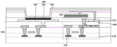
参考图1A所示,为本发明实施例提供的一种有机发光显示面板的示意图。本发明实施例所述的有机发光显示面板包括:阵列基板110、以及位于阵列基板110上的光感识别阵列,阵列基板110包括多个光感检测电路120,光感识别阵列包括多个光感识别器件130,多个光感检测电路120与多个光感识别器件130分别对应设置并电连接;光感检测电路120包括公共电压输入层121和光感检测开关122,光感检测开关122包括漏极金属层D,光感识别器件130的第一极130a电连接对应的光感检测电路120的漏极金属层D,光感识别器件130的第二极130b电连接对应的光感检测电路120的公共电压输入层121;其中,光感检测电路120的公共电压输入层121和对应的光感识别器件130的第一极130a在垂直于阵列基板110的方向上有交叠以形成有光感存储电容140。Referring to FIG. 1A , it is a schematic diagram of an organic light emitting display panel according to an embodiment of the present invention. The organic light emitting display panel according to the embodiment of the present invention includes: an
可选的,参考图1A所示的有机发光显示面板,还包括:位于阵列基板110上的多个有机发光结构150,有机发光结构150沿远离阵列基板110的方向上依次包括第一电极151、发光功能层152和第二电极153。可选发光功能层152出射的光线经过第二电极153出射。在其他可选实施例中还可选有机发光显示面板为底发光模式的有机发光显示面板或双面发光模式的有机发光显示面板,在本发明中不对有机发光显示面板的发光模式进行具体限制。Optionally, referring to the organic light emitting display panel shown in FIG. 1A , it further includes: a plurality of organic
需要说明的是,本发明实施例的有机发光显示面板中,可选多个有机发光结构150包含m种颜色有机发光结构,m个不同颜色的有机发光结构150构成一个有机发光单元,其中可选有机发光单元与光感识别器件130一一对应设置。例如参考图2A~图2C所示有机发光显示面板包括呈阵列排布的多个有机发光单元(在此仅示出2*2个有机发光单元,即有机发光单元呈2行2列阵列排布,可选m=3),多个有机发光单元与多个光感识别器件(标记为S)分别对应设置,每个有机发光单元中包括3种颜色有机发光结构且分别为红色有机发光结构R、绿色有机发光结构G和蓝色有机发光结构B。It should be noted that, in the organic light-emitting display panel according to the embodiment of the present invention, a plurality of optional organic light-
具体的,参考图2A所示,光感识别器件S与对应的有机发光单元中的红色有机发光结构R相邻设置,其中,光感识别器件S设置在对应的红色有机发光结构R的非显示区;参考图2B所示,光感识别器件S与对应的有机发光单元中的绿色有机发光结构G相邻设置,其中,光感识别器件S设置在对应的绿色有机发光结构G的非显示区;参考图2C所示,光感识别器件S与对应的有机发光单元中的蓝色有机发光结构B相邻设置,其中,光感识别器件S设置在对应的蓝色有机发光结构B的非显示区。Specifically, as shown in FIG. 2A , the light-sensing identification device S is disposed adjacent to the red organic light-emitting structure R in the corresponding organic light-emitting unit, wherein the light-sensing identification device S is disposed in the non-display area of the corresponding red organic light-emitting structure R 2B, the light-sensing identification device S is disposed adjacent to the green organic light-emitting structure G in the corresponding organic light-emitting unit, wherein the light-sensing identification device S is disposed in the non-display area of the corresponding green organic light-emitting structure G 2C, the light-sensing identification device S is arranged adjacent to the blue organic light-emitting structure B in the corresponding organic light-emitting unit, wherein the light-sensing identification device S is arranged in the non-display of the corresponding blue organic light-emitting structure B Area.
可选的,本发明实施例的有机发光显示面板还包括:位于阵列基板上的多个第一颜色有机发光结构,多个第一颜色有机发光结构与多个光感识别器件分别对应设置,以及,光感识别器件设置在对应的第一颜色有机发光结构的非显示区。具体的,参考图2A~图2B所示,可选第一颜色有机发光结构为红色有机发光结构R和/或绿色有机发光结构G。在此可选光感识别器件S/130分布在红色有机发光结构R的非显示区和/或绿色有机发光结构G的非显示区,其原因在于:光感识别器件130和光感检测电路120堆叠后,会占用有机发光结构150的一部分面积,导致有机发光结构150的发光区域减少,影响显示亮度;而红色有机发光结构R和绿色有机发光结构G的发光效率高于蓝色有机发光结构B,若牺牲蓝色有机发光结构B的发光区域用以设置光感识别器件130,则会导致蓝色有机发光结构B的发光效率远低于红绿有机发光结构,进而大幅影响有机发光显示面板的显示效果,而牺牲红色有机发光结构R和/或绿色有机发光结构G的发光区域用以设置光感识别器件130,对有机发光显示面板的显示效果的影响较小,因此光感识别器件S/130分布在红色有机发光结构R的非显示区和/或绿色有机发光结构G的非显示区。Optionally, the organic light-emitting display panel according to the embodiment of the present invention further includes: a plurality of first-color organic light-emitting structures located on the array substrate, the plurality of first-color organic light-emitting structures and the plurality of light-sensing recognition devices are respectively disposed correspondingly, and , the light-sensing identification device is arranged in the non-display area of the corresponding first-color organic light-emitting structure. Specifically, referring to FIGS. 2A to 2B , the optional first color organic light-emitting structure is a red organic light-emitting structure R and/or a green organic light-emitting structure G. Here, the optional light-sensing recognition device S/130 is distributed in the non-display area of the red organic light-emitting structure R and/or the non-display area of the green organic light-emitting structure G. The reason is that the light-
本发明实施例中,参考图1A,通常光感识别器件130的第一极130a为光感识别器件130的一金属引线,光感识别器件130的第二极130b为光感识别器件130的另一金属引线。可选本发明实施例中制作的光感识别器件130的第一极130a具有一定宽度,则光感检测电路120的公共电压输入层121和对应的光感识别器件130的第一极130a在垂直于阵列基板110的方向上能够产生交叠进而形成光感存储电容140,达到了降低成本和减少光感存储电容制作工序的效果。In the embodiment of the present invention, referring to FIG. 1A , generally, the
可选的,参考图1B所示,有机发光显示面板中光感识别器件130的第一极130a的面积较大,相应的光感识别器件130的第一极130a电连接对应的光感检测电路120的漏极金属层D的同时,光感识别器件130的第一极130a与对应的公共电压输入层121的交叠面积增大,进而提高光感存储电容140的存储能力。另一方面,除光感识别器件130的第二极130b之外,光感识别器件130的其他结构可采用一道掩膜形成,与图1A相比,减少了掩膜数,便于制造。Optionally, as shown in FIG. 1B , the area of the
可选的,参考图1B所示,光感识别器件130的第二极130b包括第一连接金属132a和第二连接金属132b,第一连接金属132a分别与第二连接金属132b和对应的光感检测电路120的公共电压输入层121电连接。需要说明的是,光感识别器件130的主体结构可选为具有光敏特性的PN结133,第二连接金属132b与PN结133直接接触,那么形成光感识别器件130的第二极130b的第一连接金属132a前,刻蚀第一连接金属132a和第二连接金属132b的连接过孔时能够以第二连接金属132b作为保护层,避免刻蚀连接过孔制程对PN结133的损伤,由此可避免对光感识别器件130的性能的影响。另一方面,图1B所示的光感识别器件130的第一极130a、PN结133和第二连接金属132b可采用一道掩膜形成,与图1A相比,减少了掩膜数,便于制造。Optionally, as shown in FIG. 1B , the
参考图1A和图1B,本发明实施例中有机发光显示面板的阵列基板110包括多个光感检测电路120,阵列基板110上还设置有光感识别阵列。光感识别器件130用于接收反射光并将接收的反射光转化为电信号,该反射光为有机发光显示面板的发射光线经由有机发光显示面板上的触摸主体反射后形成,不同光感识别器件130接收的反射光线强度不同时相应产生的电信号不同。与光感识别器件130电连接的光感检测电路120读取光感识别器件130的电信号,由此有机发光显示面板根据各光感识别器件130的电信号确定触摸主体信息。可选触摸主体为用户手指,则光感识别器件130接收的反射光为有机发光显示面板的发射光线经由手指谷脊反射的光线,有机发光显示面板能够根据光感识别器件130的电信号确定手指谷脊的纹路信息。Referring to FIG. 1A and FIG. 1B , an
另一方面,光感识别器件130根据接收的反射光线产生电信号,以及光感检测电路120读取光感识别器件130的电信号,则有机发光显示面板能够根据各光感识别器件130的电信号确定手指位置信息。On the other hand, the light-
本发明实施例中有机发光显示面板的光感识别阶段包括数据写入阶段和数据读取阶段。数据写入阶段,公共电压输入层121将公共电压信号传输至对应的光感识别器件130的第二极130b,光感检测开关122导通以使光感数据信号通过漏极金属层D传输至对应的光感识别器件130的第一极130a,则公共电压输入层121和对应的光感识别器件130的第一极130a之间形成的光感存储电容140保持第一电位。手指触摸有机发光显示面板,则光感识别器件130根据接收的反射光强度产生相应的电流变化,则光感存储电容140变化为第二电位,数据读取阶段,有机发光显示面板通过光感检测开关122读取光感存储电容140的电位信息并根据该电位信息确定手指纹路信息和/或手指位置信息。In the embodiment of the present invention, the light-sensing identification stage of the organic light-emitting display panel includes a data writing stage and a data reading stage. In the data writing stage, the common
由此可知,本发明实施例提供的有机发光显示面板,阵列基板110中设置有光感检测电路120,光感识别阵列集成在阵列基板110上,则有机发光显示面板是集成了指纹识别结构的有机发光显示阵列堆叠结构,并实现了有机发光显示与指纹识别一体的效果,还实现了内嵌式指纹识别、指纹触控和全屏幕指纹识别的效果,并且有机发光显示面板中指纹识别结构的面积大大增加,从而能够有效提高指纹识别精度;与现有技术相比,光感识别阵列集成在阵列基板110上,无需占用显示屏面积,也无需在封装玻璃上开孔,还达到了降低成本、提高面板可靠性和便于用户使用的效果。It can be seen that, in the organic light-emitting display panel provided by the embodiment of the present invention, the light-
本发明实施例提供的有机发光显示面板,复用其中一些膜层作为光感存储电容140,其中复用光感识别器件130的第一极130a作为光感存储电容140的一极,复用公共电压输入层121作为光感存储电容140的另一极,则有机发光显示面板是减少了掩膜数量的集成式堆叠结构,与现有技术相比,无需单独设置光感存储电容140,达到了降低成本和减少制作工序的效果。In the organic light-emitting display panel provided by the embodiment of the present invention, some of the film layers are multiplexed as the
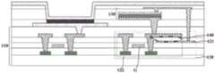
可选的,参考图3所示的有机发光显示面板,与图1A和图1B的区别在于,该有机发光显示面板中光感检测电路120中公共电压输入层121和漏极金属层D在垂直于阵列基板110的方向上有交叠以形成有光感存储电容140。图3所示的有机发光显示面板,复用其中一些膜层作为光感存储电容140,其中复用光感检测开关122的漏极金属层D作为光感存储电容140的一极,复用公共电压输入层121作为光感存储电容140的另一极,则有机发光显示面板是减少了掩膜数量的集成式堆叠结构,与现有技术相比,无需单独设置光感存储电容140,达到了降低成本和减少制作工序的效果。Optionally, referring to the organic light emitting display panel shown in FIG. 3 , the difference from FIG. 1A and FIG. 1B is that the common
可选的,参考图1A~图3所示的有机发光显示面板,光感检测电路120的公共电压输入层121与有机发光结构150的第一电极151同层。本实施例中采用一个掩膜(mask)同时形成公共电压输入层121和有机发光结构150的第一电极151,公共电压输入层121和有机发光结构150的第一电极151的材料相同,不仅能够减少一道mask工序,还可以减少一层绝缘层与金属层,进一步达到了降低成本、减少制作工序和减小有机发光显示面板厚度的效果。Optionally, referring to the organic light emitting display panel shown in FIGS. 1A to 3 , the common
可选的,参考图4所示的有机发光显示面板,光感检测开关122还包括第一栅极G。光感识别阶段,给光感检测开关122的第一栅极G施加使光感检测开关122导通的驱动信号,则光感检测开关122导通以使光感数据信号通过漏极金属层D传输至对应的光感识别器件130,以及,光感检测开关122导通以通过漏极金属层D读取光感识别器件130中光感存储电容140的电位信息,以确定触控主体信息。Optionally, referring to the organic light emitting display panel shown in FIG. 4 , the light
可选的,参考图4所示的有机发光显示面板,与图1A-图3的区别在于,光感检测电路120的公共电压输入层121与光感检测开关122的第一栅极G同层。则光感检测电路120中公共电压输入层121和漏极金属层D在垂直于阵列基板110的方向上有交叠以形成有光感存储电容140。本实施例中采用一个掩膜(mask)同时形成公共电压输入层121和光感检测开关122的第一栅极G,公共电压输入层121和光感检测开关122的第一栅极G的材料相同,公共电压输入层121作为光感存储电容140的一极,不仅能够减少一道mask工序,还可以减少一层绝缘层与金属层,进一步达到了降低成本、减少制作工序和减小有机发光显示面板厚度的效果。Optionally, referring to the organic light emitting display panel shown in FIG. 4 , the difference from FIGS. 1A to 3 is that the common
可选的,参考图5所示的有机发光显示面板,光感检测开关122还包括第一栅极G。与图1A-图4的区别在于,图5所示的有机发光显示面板中光感检测电路120的公共电压输入层121位于光感检测开关122的第一栅极G所在膜层和光感检测开关122的漏极金属层D所在膜层之间。则光感检测电路120中公共电压输入层121和漏极金属层D在垂直于阵列基板110的方向上有交叠以形成有光感存储电容140。本实施例中公共电压输入层121复用为光感存储电容140的一极,漏极金属层D复用为光感存储电容140的另一极,无需单独制作光感存储电容,相应降低了有机发光显示面板的制作成本和制作工序,并能够达到减小有机发光显示面板厚度的效果。Optionally, referring to the organic light emitting display panel shown in FIG. 5 , the light
可选的,参考图6所示的有机发光显示面板,与图1A-图5的区别在于,阵列基板110还包括像素存储电容160,像素存储电容160的第一极161与光感检测开关122的第一栅极G同层,像素存储电容160的第二极162与公共电压输入层121同层。则光感检测电路120中公共电压输入层121和漏极金属层D在垂直于阵列基板110的方向上有交叠以形成有光感存储电容140。本实施例中采用一个掩膜(mask)同时形成公共电压输入层121和像素存储电容160的第二极162,公共电压输入层121和像素存储电容160的第二极162的材料相同,不仅能够减少一道mask工序,还可以减少一层绝缘层与金属层,进一步达到了降低成本、减少制作工序和减小有机发光显示面板厚度的效果。Optionally, referring to the organic light emitting display panel shown in FIG. 6 , the difference from FIG. 1A to FIG. 5 is that the
可选的,参考图7所示的有机发光显示面板,与图1A-图6的区别在于,光感检测开关122的漏极金属层D包括第一漏极D1和与该第一漏极D1电连接的补偿漏极层D2,补偿漏极层D2和第一漏极D1不同层,光感识别器件130的第一极130a电连接对应的光感检测电路120的第一漏极D1;光感检测电路120中,公共电压输入层121位于第一漏极D1所在膜层和补偿漏极层D2之间,以及公共电压输入层121分别与第一漏极D1和补偿漏极层D2在垂直于阵列基板110的方向上有交叠。则光感检测电路120中公共电压输入层121和对应的第一漏极D1形成有光感存储电容140,同时公共电压输入层121和对应的补偿漏极层D2形成有光感存储电容140。Optionally, referring to the organic light emitting display panel shown in FIG. 7 , the difference from FIG. 1A to FIG. 6 is that the drain metal layer D of the
本实施例中无需单独制作光感存储电容,相应降低了有机发光显示面板的制作成本和制作工序,并能够达到减小有机发光显示面板厚度的效果;以及,公共电压输入层121设置在第一漏极D1所在膜层和补偿漏极层D2所在膜层之间,有效增加了光感存储电容140的面积,从而能够进一步提高光感识别性能,提高指纹识别精确度。In this embodiment, there is no need to separately manufacture the photosensitive storage capacitor, which reduces the manufacturing cost and manufacturing process of the organic light-emitting display panel, and can achieve the effect of reducing the thickness of the organic light-emitting display panel; and, the common
可选的,参考图7所示的有机发光显示面板,补偿漏极层D2可和光感检测开关122的第一栅极G同层。本实施例中采用一个掩膜(mask)同时形成第一栅极G和补偿漏极层D2,第一栅极G和补偿漏极层D2的材料相同,则不仅能够减少一道mask工序,还可以减少一层绝缘层与金属层,进一步达到了降低成本、减少制作工序和减小有机发光显示面板厚度的效果,以及达到了有效增加光感存储电容140的面积的效果,并进一步达到了提高光感识别性能和提高指纹识别精确度的效果。Optionally, referring to the organic light emitting display panel shown in FIG. 7 , the compensation drain layer D2 may be the same layer as the first gate G of the light
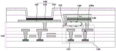
可选的,参考图8所示的有机发光显示面板,光感检测电路120中公共电压输入层121和对应的光感识别器件130的第一极130a之间形成有光感存储电容140。本实施例中无需单独制作光感存储电容,相应降低了有机发光显示面板的制作成本和制作工序,并能够达到减小有机发光显示面板厚度的效果。Optionally, referring to the organic light emitting display panel shown in FIG. 8 , a
可选的,参考图8所示的有机发光显示面板,与图1A-图7的区别在于,光感识别器件130的第一极130a与有机发光结构150的第一电极151同层。本实施例中采用一个掩膜(mask)同时形成第一电极151和光感识别器件130的第一极130a,第一电极151和光感识别器件130的第一极130a的材料相同,则不仅能够减少一道mask工序,还可以减少一层绝缘层与金属层,进一步达到了降低成本、减少制作工序和减小有机发光显示面板厚度的效果。Optionally, referring to the organic light emitting display panel shown in FIG. 8 , the difference from FIGS. 1A to 7 is that the
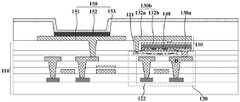
可选的,参考图9所示的有机发光显示面板,光感识别器件130的第二极130b包括第一连接金属132a和第二连接金属132b,第一连接金属132a分别与第二连接金属132b和对应的光感检测电路120的公共电压输入层121电连接。其中可选光感检测电路120中公共电压输入层121和对应的光感识别器件130的第一极130a之间形成有光感存储电容140。本实施例中无需单独制作光感存储电容,相应降低了有机发光显示面板的制作成本和制作工序,并能够达到减小有机发光显示面板厚度的效果。Optionally, referring to the organic light emitting display panel shown in FIG. 9 , the
可选的,参考图9所示的有机发光显示面板,与图1A-图8的区别在于,第一连接金属132a与有机发光结构150的第一电极151同层。本实施例中采用一个掩膜(mask)同时同层形成第一电极151和第一连接金属132a,第一电极151和第一连接金属132a的材料相同,则不仅能够减少一道mask工序,还可以减少一层绝缘层与金属层,进一步达到了降低成本、减少制作工序和减小有机发光显示面板厚度的效果。Optionally, referring to the organic light emitting display panel shown in FIG. 9 , the difference from FIGS. 1A to 8 is that the
可选的,参考图10所示的有机发光显示面板,与图1A-图9的区别在于,光感检测开关122的漏极金属层D复用为光感识别器件130的第一极130a。则可选光感检测电路120中公共电压输入层121和对应的光感检测开关122的漏极金属层D之间形成有光感存储电容140。有机发光显示面板的第一电极151通常为ITO-Ag-ITO结构,而光感识别器件130在制作过程中需要经过多次湿刻及干刻工艺,可能影响有机发光显示面板的第一电极151的功函数及表面状况,进而影响有机发光显示面板的发光效率。Optionally, referring to the organic light emitting display panel shown in FIG. 10 , the difference from FIGS. 1A to 9 is that the drain metal layer D of the light
本实施例中光感检测开关122的漏极金属层D复用为光感识别器件130的第一极130a,则直接以漏极金属层D为光感识别器件130的第一极130a制作光感识别器件130,则光感识别器件130在制作过程中的经过多次湿刻及干刻工艺完成之后再进行有机发光显示面板的第一电极151的形成,因此光感识别器件130的多次湿刻及干刻工艺不会影响有机发光显示面板的第一电极151的功函数及表面状况,也不会影响有机发光显示面板的发光效率。本实施例中光感识别器件130采用的mask减少,且无需单独制作光感存储电容,相应降低了有机发光显示面板的制作成本和制作工序,并能够达到减小有机发光显示面板厚度的效果。In this embodiment, the drain metal layer D of the
可选的,在上述图1A-图10的基础上,参考图11所示的有机发光显示面板,其中,光感识别器件130包括具有光敏特征的PN结133,PN结133包括依次层叠的P型掺杂半导体层133a、非晶硅层133b和N型掺杂半导体层133c,P型掺杂半导体层133a电连接对应的光感检测电路120的公共电压输入层121以及N型掺杂半导体层133c电连接对应的光感检测电路120的漏极金属层D。Optionally, on the basis of the above-mentioned FIGS. 1A-10 , with reference to the organic light-emitting display panel shown in FIG. 11 , the light-
光感检测开关122还包括源极,该源极电连接光感数据线(未示出),光感数据线用于给光感识别器件130传输光感数据信号以及光照后用于读取光感识别器件130的光感存储电容140的电位信息。光感识别器件130通常处于偏置状态,PN结133的P型掺杂半导体层133a电连接公共电压输入层121,以及N型掺杂半导体层133c电连接漏极金属层D,则可选公共电压输入层121的电位为-5V,光感数据线的写入光感数据信号的电位为1.8V。The light-sensing
可选的,参考图12所示的有机发光显示面板,与图11的区别在于,P型掺杂半导体层133a电连接对应的光感检测电路120的漏极金属层D以及N型掺杂半导体层133c电连接对应的光感检测电路120的公共电压输入层121。则为了保证光感识别器件130处于偏置状态以正常工作,可选公共电压输入层121的电位为5V,光感数据线的写入光感数据信号的电位为-1.8V。Optionally, referring to the organic light emitting display panel shown in FIG. 12 , the difference from FIG. 11 is that the P-type doped semiconductor layer 133 a is electrically connected to the drain metal layer D and the N-type doped semiconductor layer of the corresponding
需要说明的是,上述图1A-图12仅示出了有机发光显示面板的部分结构,未示出有机发光显示面板的全部结构,有机发光显示面板的其他结构可参考现有有机发光显示面板,在此不再赘述。本领域技术人员可以理解,有机发光显示面板中光感识别器件和光感检测电路的设置方式包括但不限于以上示例,在不影响有机发光显示面板的显示功能的前提下,上述多种光感识别器件和光感检测电路的设置方式可以进行相互结合和重组,在此不再详述,本领域技术人员也可以理解,本发明实施例提供的有机发光显示面板包括但不限于下述示例。It should be noted that the above-mentioned FIGS. 1A to 12 only show part of the structure of the organic light-emitting display panel, but not the entire structure of the organic light-emitting display panel. For other structures of the organic light-emitting display panel, reference may be made to the existing organic light-emitting display panel. It is not repeated here. Those skilled in the art can understand that the arrangement of the light-sensing identification device and the light-sensing detection circuit in the organic light-emitting display panel includes, but is not limited to, the above examples. The arrangement of the device and the light sensing detection circuit can be combined and recombined, which will not be described in detail here. Those skilled in the art can also understand that the organic light emitting display panel provided by the embodiment of the present invention includes but is not limited to the following examples.
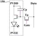
可选的,参考图13A所示,为上述任意有机发光显示面板中像素的等效电路,其中,像素包括有机发光结构150和与有机发光结构150电连接的像素开关Tp,像素开关Tp的源极电连接数据线Data,像素开关Tp的栅极电连接扫描线Gate,像素开关Tp的漏极电连接有机发光结构150。有机发光结构150包括第一电极、发光功能层和第二电极,在第一电极和第二电极上分别施加PVDD和PVEE电压信号,则有机发光结构150发射光线。有机发光结构150发射的光线可以作为光感识别器件的光源。Optionally, referring to FIG. 13A, it is an equivalent circuit of a pixel in any of the above-mentioned organic light-emitting display panels, wherein the pixel includes an organic light-emitting
可选的,参考图13B所示,为上述任意有机发光显示面板中光感等效电路,其中,光感等效电路包括光感识别器件130和与光感识别器件130电连接的光感检测电路120。可选光感检测电路120的光感检测开关Tps的源极电连接光感数据线Datas,光感检测开关Tps的栅极电连接光感扫描线Gates,光感检测开关Tps的漏极金属层电连接光感识别器件130且该漏极金属层作为光感存储电容Cst的一极。光感识别器件130包括具有光敏特性的PIN结,可选PIN结的正极电连接公共电压输入层Vcom,PIN结的负极电连接光感检测开关Tps的漏极金属层,公共电压输入层Vcom和光感检测开关Tps的漏极金属层之间形成光感存储电容Cst。光感识别阶段包括数据写入阶段,此时光感检测开关Tps导通,公共电压输入层Vcom的公共电压信号和光感数据线Datas的光感数据信号写入光感存储电容Cst,则光感存储电容Cst上形成固定的电压差;光感识别阶段还包括数据读取阶段,手指触摸有机发光显示面板,则光感识别器件130根据接收的反射光强度产生相应的电流变化使得光感存储电容Cst的电位,数据读取阶段,光感检测开关Tps导通,则有机发光显示面板通过光感数据线Datas读取光感存储电容Cst的电位信息,由此有机发光显示面板可根据光感存储电容Cst的写入电位信息和读取电位信息,确定手指纹路信息和/或手指位置信息。Optionally, as shown in FIG. 13B , it is a light-sensing equivalent circuit in any of the above-mentioned organic light-emitting display panels, wherein the light-sensing equivalent circuit includes a light-
可选的,参考图14所示,为本发明实施例提供的一种有机发光显示面板的制造方法,该制造方法包括:Optionally, referring to FIG. 14 , a method for manufacturing an organic light-emitting display panel provided in an embodiment of the present invention includes:
步骤210、提供一阵列基板,阵列基板包括多个光感检测电路,光感检测电路包括公共电压输入层和光感检测开关,光感检测开关包括漏极金属层;
步骤220、在阵列基板上形成光感识别阵列,光感识别阵列包括多个光感识别器件,多个光感检测电路与多个光感识别器件分别对应设置并电连接,光感识别器件的第一极电连接对应的光感检测电路的漏极金属层,光感识别器件的第二极电连接对应的光感检测电路的公共电压输入层;
其中,光感检测电路的公共电压输入层和对应的光感识别器件的第一极在垂直于阵列基板的方向上有交叠以形成有光感存储电容,或者,光感检测电路中公共电压输入层和漏极金属层在垂直于阵列基板的方向上有交叠以形成有光感存储电容。Wherein, the common voltage input layer of the photosensitive detection circuit and the first pole of the corresponding photosensitive identification device are overlapped in the direction perpendicular to the array substrate to form a photosensitive storage capacitor, or, the common voltage in the photosensitive detection circuit The input layer and the drain metal layer overlap in a direction perpendicular to the array substrate to form a photosensitive storage capacitor.
本发明实施例提供的有机发光显示面板的结构与现有技术不同,但制备各个膜层所采用的工艺方法有多种,在此不具体限制和说明,可现有制备工艺方法制备本发明实施例提供的有机发光显示面板,例如可采用湿法刻蚀和干法刻蚀等工艺形成光感检测开关和像素开关的各个膜层等。The structure of the organic light-emitting display panel provided by the embodiment of the present invention is different from that of the prior art, but there are various process methods for preparing each film layer, which are not specifically limited and described here. For example, in the organic light-emitting display panel provided, for example, processes such as wet etching and dry etching can be used to form the photosensitive detection switches and the respective film layers of the pixel switches.
采用上述制作方法形成的有机发光显示面板的结构是集成了指纹识别结构的有机发光显示阵列堆叠结构,实现了有机发光显示与指纹识别一体的效果,还实现了内嵌式指纹识别、指纹触控和全屏幕指纹识别的效果,并且有机发光显示面板中指纹识别结构的面积大大增加,从而能够有效提高指纹识别精度;与现有技术相比,光感识别阵列集成在阵列基板上,无需占用显示屏面积,也无需在封装玻璃上开孔,还达到了降低成本、提高面板可靠性和便于用户使用的效果;以及复用其中一些膜层作为光感存储电容,则有机发光显示面板是减少了掩膜数量的集成式堆叠结构,与现有技术相比,无需单独设置光感存储电容,达到了降低成本和减少制作工序的效果。The structure of the organic light-emitting display panel formed by the above manufacturing method is an organic light-emitting display array stack structure integrated with a fingerprint identification structure, which realizes the integration of organic light-emitting display and fingerprint identification, and also realizes embedded fingerprint identification and fingerprint touch control. And the effect of full-screen fingerprint recognition, and the area of the fingerprint recognition structure in the organic light-emitting display panel is greatly increased, which can effectively improve the fingerprint recognition accuracy; The screen area does not need to be opened on the encapsulating glass, and it also achieves the effects of reducing costs, improving the reliability of the panel, and being user-friendly; and reusing some of the film layers as photosensitive storage capacitors, the organic light-emitting display panel is reduced. Compared with the prior art, the integrated stack structure with the number of masks does not need to separately set a photosensitive storage capacitor, thereby achieving the effects of reducing costs and manufacturing processes.
可选的,本发明实施例还提供了一种有机发光显示装置的指纹识别方法,参考图15所示该有机发光显示装置包括:如上任一所述的有机发光显示面板310和位于有机发光显示面板310上的盖板320,其中,盖板320的背离有机发光显示面板310的第一表面为有机发光显示装置的出光表面。Optionally, an embodiment of the present invention further provides a fingerprint identification method for an organic light-emitting display device. Referring to FIG. 15 , the organic light-emitting display device includes: the organic light-emitting
参考图16所示,图15所示有机发光显示装置的指纹识别方法包括:Referring to FIG. 16 , the fingerprint identification method of the organic light-emitting display device shown in FIG. 15 includes:
步骤410、指纹识别阶段,控制各有机发光结构按照第一发光点阵位移发光,其中第一发光点阵中任意相邻两个有机发光结构的距离大于或等于最小无串扰距离,最小无串扰距离为任一有机发光结构发出的光经过盖板的第一表面反射后在光感识别阵列上形成的覆盖区域的最大半径。Step 410: In the fingerprint identification stage, control each organic light-emitting structure to emit light according to the displacement of the first light-emitting lattice, wherein the distance between any two adjacent organic light-emitting structures in the first light-emitting lattice is greater than or equal to the minimum crosstalk-free distance, and the minimum crosstalk-free distance The maximum radius of the coverage area formed on the light-sensing recognition array after the light emitted by any organic light-emitting structure is reflected by the first surface of the cover plate.
步骤420、光感识别阵列根据经由盖板的第一表面上的触摸主体反射到各光感识别器件的光线进行指纹识别。本发明实施例中触摸主体可选为用户手指。Step 420: The light-sensing identification array performs fingerprint identification according to the light reflected to each light-sensing identification device via the touch body on the first surface of the cover plate. In this embodiment of the present invention, the touch body can be selected as a user's finger.
本发明实施例所述的有机发光显示装置采用画面扫描方式进行指纹识别方法,一个画面中各个有机发光结构按照第一发光点阵位移发光。基于第一发光点阵中任意相邻两个有机发光结构的距离大于或等于最小无串扰距离,第一发光点阵中任意一个有机发光结构出射的光线经过用户手指的指纹反射后形成的指纹反射光不会照射到该点阵中其他有机发光结构所对应的光感识别器件上,因此第一发光点阵中每个有机发光结构所对应的光感识别器件均只能够接收到与其对应的有机发光结构的出射光线形成的指纹反射光,即光感识别器件不会受到其他有机发光结构的串扰信号。相应的,光感识别器件产生的感应信号准确反应了对应的有机发光结构的出射光线在用户手指的指纹上的反射,因此本发明实施例提供的有机发光显示装置提高了指纹识别精确度。The organic light-emitting display device according to the embodiment of the present invention adopts the screen scanning method to perform the fingerprint identification method, and each organic light-emitting structure in a screen emits light according to the displacement of the first light-emitting lattice. Based on the distance between any two adjacent organic light-emitting structures in the first light-emitting lattice is greater than or equal to the minimum crosstalk-free distance, the fingerprint reflection formed by the light emitted by any organic light-emitting structure in the first light-emitting lattice is reflected by the fingerprint of the user's finger The light will not be irradiated on the light-sensing recognition devices corresponding to other organic light-emitting structures in the lattice, so the light-sensing recognition devices corresponding to each organic light-emitting structure in the first light-emitting lattice can only receive the corresponding organic light-emitting structure. The fingerprints formed by the light emitted from the light-emitting structure reflect light, that is, the light-sensing recognition device will not be subjected to crosstalk signals from other organic light-emitting structures. Correspondingly, the sensing signal generated by the light-sensing recognition device accurately reflects the reflection of the emitted light of the corresponding organic light-emitting structure on the fingerprint of the user's finger. Therefore, the organic light-emitting display device provided by the embodiment of the present invention improves the fingerprint recognition accuracy.
参考图15和图16,指纹识别阶段,本发明实施例提供的有机发光显示装置采用有机发光结构150作为光感识别器件130的光源进行指纹识别。用户手指按压在盖板320的第一表面时,有机发光结构150出射的光线经过盖板320的第一表面照射到用户手指上,用户手指的指纹反射形成反射光且该指纹反射光从盖板320的第一表面入射并照射到与发光的有机发光结构150对应的光感识别器件130上,接收到指纹反射光的光感识别器件130产生感应信号,由此进行指纹识别。通过第一发光点阵来作为光感识别器件130的检测光源是因为有机发光结构150出射的光线具有较大范围的角度分布。而若采用有机发光显示面板中所有有机发光结构同时发光进行指纹识别,则每一个光感识别器件除了接收所对应有机发光结构的指纹反射光之外,还会接收到其他多个有机发光结构的串扰信号,导致指纹识别精确度低。Referring to FIGS. 15 and 16 , in the fingerprint identification stage, the organic light-emitting display device provided by the embodiment of the present invention uses the organic light-emitting
可选的图17A~图17C是本发明实施例提供的三种第一发光点阵的示意图。Optionally, FIG. 17A to FIG. 17C are schematic diagrams of three kinds of first light-emitting lattices provided by the embodiments of the present invention.
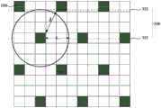
参考图17A所示第一发光点阵330为五方发光点阵,五方发光点阵包括一中心有机发光结构150和五个边缘有机发光结构150。第一发光点阵330的多个有机发光结构150构成多个图形,多个图形中面积最小图形331的各个角的角度不等于90°。五方发光点阵能够在确保无信号串扰的基础上提升同一时间点亮的有机发光结构150个数,减小读取指纹所需时间。Referring to FIG. 17A , the first light-emitting
参考图17B所示第一发光点阵330为六方发光点阵,六方发光点阵包括一中心有机发光结构150和六个边缘有机发光结构150。六方发光点阵能够在确保无信号串扰的基础上提升同一时间点亮的有机发光结构150个数,减小读取指纹所需时间。Referring to FIG. 17B , the first light-emitting
参考图17C所示第一发光点阵330为间隔设置的第一发光行332和第二发光行333,其中第一发光行332中的任一有机发光结构150和第二发光行333中的任一有机发光结构150位于不同列。该第一发光点阵330能够在确保无信号串扰的基础上提升同一时间点亮的有机发光结构150个数,从而显著减小了读取指纹所需时间。Referring to FIG. 17C , the first light-emitting
对于上述任意实施例提供的任意一种第一发光点阵330,可选第一发光点阵330中任意相邻两个有机发光结构150的距离J等于最小无串扰距离L。显然,第一发光点阵330中每个发光有机发光结构150所对应的光感识别器件130不会受到同时发光的其他有机发光结构的串扰信号,保证了指纹信号的准确性;同时,第一发光点阵330中任意相邻两个有机发光结构150的距离J等于最小无串扰距离L,也能够使同一时间点亮的有机发光结构150个数较多,减小读取指纹信号所需时间,提高读取指纹效率。For any one of the first light-emitting
对于上述任意实施例提供的任意一种第一发光点阵330,可选对于第一发光点阵330中位于不同行的任意相邻两个有机发光结构150,一有机发光结构150到另一有机发光结构150所在行的垂直距离C1(图17B示例)小于最小无串扰距离L;和/或,对于第一发光点阵330中位于不同列的任意相邻两个有机发光结构150,一有机发光结构150到另一有机发光结构150所在列的垂直距离C2(图17B示例)小于最小无串扰距离L。For any one of the first light-emitting
为了提高指纹识别精确度,在指纹识别阶段,多个有机发光结构150按照第一发光点阵330位移发光,第一发光点阵330中任意相邻两个有机发光结构150的距离J大于或等于最小无串扰距离L。有机发光结构150出射的光线具有角度分布,则有机发光结构150发出的光经过盖板320的第一表面反射后会在光感识别阵列上形成一个覆盖区域,该有机发光结构150发出的任意角度光的指纹反射光均会落入该覆盖区域内,其中该覆盖区域的最大半径即为最小无串扰距离L。In order to improve the accuracy of fingerprint identification, in the fingerprint identification stage, the plurality of organic light-emitting
本发明实施例中第一发光点阵330中任意相邻两个有机发光结构150的距离J大于或等于最小无串扰距离L,则其中任意一个发光有机发光结构150的指纹反射光始终不会照射到同时发光的其它有机发光结构150所对应的光感识别器件130上,即第一发光点阵330中任意一个有机发光结构150所对应的光感识别器件130均只能够接收到与其对应的有机发光结构150的指纹反射光。因此光感识别器件130不会受到其它有机发光结构的串扰信号,提高了有机发光显示装置的指纹识别精确度。In the embodiment of the present invention, the distance J between any two adjacent organic light-emitting
需要说明的是,指纹反射光是按压在盖板320的第一表面的用户手指的指纹对有机发光结构150出射光线进行反射所形成的反射光,而用户手指的指纹和盖板320的第一表面之间的距离相对于有机发光显示装置的厚度非常小,对覆盖区域的范围影响较小,因此本发明实施例中设置最小无串扰距离L时略去了用户手指和盖板320的第一表面之间的反射距离。此外,覆盖区域的半径L实质上应以有机发光结构150的中心点为原点进行计算,但是实际的有机发光显示装置中有机发光结构150数量非常多,相应的有机发光结构150尺寸小,因此本发明实施例中可将有机发光结构150整体看作为覆盖区域的原点,则覆盖区域的半径L可表示为有机发光结构150的边缘到覆盖区域的边缘的长度,有机发光结构150的尺寸可以不计入最小无串扰距离L中。本领域技术人员可以理解,最小无串扰距离L与有机发光显示装置的厚度、有机发光结构的出光角度等因素相关,因此不同有机发光显示装置的最小无串扰距离L数值不同,在其他可选实施例中还可选有机发光结构的尺寸计入最小无串扰距离中,在本发明中不进行具体限制。It should be noted that the fingerprint reflected light is the reflected light formed by the fingerprint of the user's finger pressed on the first surface of the
需要说明的是,若有机发光显示面板310包括3种颜色子像素分别标记为R、G、B,则一个有机发光结构150包括3个不同颜色的子像素。指纹反射信号基本是镜面反射,反射角=入射角,由此可知L=tanθ*H1+tanθ*H2,其中,L为最小无串扰距离,θ为有机发光结构150的预设辉度所对应方向与垂直有机发光显示面板310方向的夹角,H1为盖板320的第一表面到发光功能层152的垂直高度,H2为盖板320的第一表面到光感识别阵列的垂直高度,预设辉度为小于或等于垂直有机发光显示面板310方向的辉度的10%。It should be noted that, if the organic light-emitting
本发明实施例中有机发光结构150出射的光线的角度与有机发光结构150的辉度相关,辉度是对(消色)发光强度的主观感受。本发明实施例中定义有机发光结构150的垂直方向上的辉度为100%,辉度百分比越低,所对应的出光角度(与垂直有机发光层方向的夹角)越大,相应的发光强度越弱。而当有机发光结构150的辉度小于或等于10%时,有机发光结构150出射的光线的发光强度非常弱,其在盖板320的第一表面形成的反射光不会对光感识别器件130造成串扰,因此本发明实施例中设定有机发光结构150的出光角度以辉度10%为临界值。基于此,确定θ的过程为:测量有机发光结构150在垂直方向上的辉度,确定垂直有机发光显示面板310方向的辉度的10%所对应的位置,根据该位置方向与垂直有机发光显示面板310方向的夹角确定θ。本领域技术人员可以理解,不同有机发光显示装置的有机发光结构发光强度可能不同,相应的预设辉度值也可能不同,例如在其他可选实施例中预设辉度值可选为垂直有机发光显示面板方向的辉度的12%或9%等,在本发明中不进行具体限制。In the embodiment of the present invention, the angle of the light emitted by the organic
如图18所示为有机发光显示装置的扫描示意图,指纹识别阶段,有机发光显示装置采用画面扫描的方式进行指纹识别。具体的,同一时间按照第一发光点阵330点亮有机发光结构150,并记录点亮的有机发光结构150对应位置的光感识别器件130产生的感应信号;在下一画面,同一时间点亮的有机发光结构150位移并记录对应的感应信号;直至循环点亮完所有有机发光结构150,并根据获取的各光感识别器件130的感应信号进行指纹识别,由于本发明实施例的光感识别器件130不会受到串扰信号,因此指纹识别精确度非常高。本领域技术人员可以理解,第一发光点阵可选是同时发光的多个有机发光结构构成的最小重复单元,并非限定为同时发光的多个有机发光结构构成的点阵。FIG. 18 is a schematic diagram of scanning of the organic light-emitting display device. In the fingerprint identification stage, the organic light-emitting display device performs fingerprint identification by means of screen scanning. Specifically, the organic light-emitting
需要说明的是,本发明实施例的有机发光显示装置采用画面扫描方式读取指纹信息,显然,若一帧画面中点亮的有机发光结构150的个数少,则完成指纹信息读取的画面帧数越多,指纹信息读取所需时间越长。为了减小了读取指纹所需时间,可选的第一发光点阵330的多个有机发光结构150构成多个图形,多个图形中面积最小图形的各个角的角度不等于90°,能够在确保无信号串扰的基础上提升同一时间点亮的有机发光结构150个数,从而显著减小了读取指纹所需时间。It should be noted that the organic light-emitting display device according to the embodiment of the present invention uses a screen scanning method to read fingerprint information. Obviously, if the number of organic light-emitting
本发明实施例还提供了一种电子设备,该电子设备包括如上任一所述的有机发光显示面板,该电子设备可以是智能手机、平板电脑等任意一种可以配备有机发光显示面板的有机发光显示设备,在本发明中不对电子设备进行具体限制。An embodiment of the present invention also provides an electronic device, the electronic device includes the organic light-emitting display panel described above, and the electronic device can be any organic light-emitting display panel that can be equipped with an organic light-emitting display panel, such as a smart phone, a tablet computer, etc. A display device, an electronic device is not specifically limited in the present invention.
注意,上述仅为本发明的较佳实施例及所运用技术原理。本领域技术人员会理解,本发明不限于这里所述的特定实施例,对本领域技术人员来说能够进行各种明显的变化、重新调整、相互结合和替代而不会脱离本发明的保护范围。因此,虽然通过以上实施例对本发明进行了较为详细的说明,但是本发明不仅仅限于以上实施例,在不脱离本发明构思的情况下,还可以包括更多其他等效实施例,而本发明的范围由所附的权利要求范围决定。Note that the above are only preferred embodiments of the present invention and applied technical principles. Those skilled in the art will understand that the present invention is not limited to the specific embodiments described herein, and various obvious changes, readjustments, combinations and substitutions can be made by those skilled in the art without departing from the protection scope of the present invention. Therefore, although the present invention has been described in detail through the above embodiments, the present invention is not limited to the above embodiments, and can also include more other equivalent embodiments without departing from the concept of the present invention. The scope is determined by the scope of the appended claims.
Claims (16)
Priority Applications (2)
| Application Number | Priority Date | Filing Date | Title |
|---|---|---|---|
| CN201710432778.3ACN107425038B (en) | 2017-06-09 | 2017-06-09 | Organic light-emitting display panel, manufacturing method thereof and electronic device |
| US15/790,828US10747978B2 (en) | 2017-06-09 | 2017-10-23 | Organic light-emitting display panel manufacturing method thereof as well as electronic device |
Applications Claiming Priority (1)
| Application Number | Priority Date | Filing Date | Title |
|---|---|---|---|
| CN201710432778.3ACN107425038B (en) | 2017-06-09 | 2017-06-09 | Organic light-emitting display panel, manufacturing method thereof and electronic device |
Publications (2)
| Publication Number | Publication Date |
|---|---|
| CN107425038A CN107425038A (en) | 2017-12-01 |
| CN107425038Btrue CN107425038B (en) | 2020-01-21 |
Family
ID=60429637
Family Applications (1)
| Application Number | Title | Priority Date | Filing Date |
|---|---|---|---|
| CN201710432778.3AActiveCN107425038B (en) | 2017-06-09 | 2017-06-09 | Organic light-emitting display panel, manufacturing method thereof and electronic device |
Country Status (2)
| Country | Link |
|---|---|
| US (1) | US10747978B2 (en) |
| CN (1) | CN107425038B (en) |
Families Citing this family (58)
| Publication number | Priority date | Publication date | Assignee | Title |
|---|---|---|---|---|
| US10770522B2 (en)* | 2017-07-10 | 2020-09-08 | Sharp Kabushiki Kaisha | EL device, manufacturing method for EL device, and manufacturing apparatus for EL device |
| CN107423723B (en)* | 2017-08-09 | 2020-02-21 | 京东方科技集团股份有限公司 | A pattern recognition device, an array substrate and a display device |
| WO2019037098A1 (en)* | 2017-08-25 | 2019-02-28 | Shenzhen Yungyinggu Technology Co., Ltd. | Integrated display and sensing apparatus |
| EP3724922A4 (en)* | 2017-12-15 | 2021-07-14 | Boe Technology Group Co., Ltd. | Amoled display panel having image scanning function |
| CN207849005U (en)* | 2018-02-02 | 2018-09-11 | 深圳市奥拓电子股份有限公司 | LED lamp bead and LED show structure |
| US20190280051A1 (en)* | 2018-03-09 | 2019-09-12 | Int Tech Co., Ltd. | Electroluminescent display integrated with touch sensor and method of forming the same |
| CN108470783B (en)* | 2018-03-28 | 2020-12-01 | 京东方科技集团股份有限公司 | Photosensitive element and its manufacturing method, display panel and its manufacturing method |
| CN108615008B (en) | 2018-04-24 | 2020-10-27 | 武汉天马微电子有限公司 | A display panel and display device |
| CN108596113B (en)* | 2018-04-27 | 2021-01-22 | 京东方科技集团股份有限公司 | Fingerprint identification device, display panel and manufacturing method thereof |
| CN108647606B (en)* | 2018-04-28 | 2020-07-14 | 武汉天马微电子有限公司 | Display panel and display device |
| CN108647669A (en)* | 2018-05-22 | 2018-10-12 | 武汉天马微电子有限公司 | Display module, preparation method thereof and display device |
| CN108805055B (en)* | 2018-05-29 | 2021-03-23 | 武汉天马微电子有限公司 | Display panel and display device |
| US10977475B2 (en)* | 2018-07-09 | 2021-04-13 | Silicon Display Technology | Fingerprint recognition sensor and display device having the same |
| CN108878503B (en)* | 2018-07-26 | 2021-01-05 | 京东方科技集团股份有限公司 | OLED display substrate, manufacturing method thereof, OLED display panel and display device |
| CN108615753B (en)* | 2018-08-02 | 2020-07-28 | 京东方科技集团股份有限公司 | An OLED array substrate, its preparation method, and display device |
| CN110827762B (en)* | 2018-08-14 | 2021-07-09 | 云谷(固安)科技有限公司 | Display panel, display screen and control method thereof, and display terminal |
| WO2020053932A1 (en)* | 2018-09-10 | 2020-03-19 | シャープ株式会社 | Display device |
| CN109473467B (en)* | 2018-12-13 | 2021-02-26 | 武汉华星光电半导体显示技术有限公司 | Display panel with photosensitive function and electronic device |
| KR102834643B1 (en)* | 2018-12-26 | 2025-07-18 | 삼성디스플레이 주식회사 | Display device |
| US11296155B2 (en)* | 2019-01-04 | 2022-04-05 | Beijing Boe Display Technology Co., Ltd. | Display panel and operation method thereof |
| CN109742113B (en) | 2019-01-08 | 2020-12-25 | 京东方科技集团股份有限公司 | Array substrate, preparation method thereof and related device |
| CN109858398B (en)* | 2019-01-14 | 2023-06-06 | 京东方科技集团股份有限公司 | Display panel, manufacturing method thereof, display device, and fingerprint identification method |
| CN109891487B (en)* | 2019-01-29 | 2022-02-01 | 京东方科技集团股份有限公司 | Display substrate, display panel, preparation method of display substrate and driving method |
| CN109920830B (en)* | 2019-03-22 | 2021-02-02 | 京东方科技集团股份有限公司 | Display panel, driving method thereof and display device |
| CN109786433B (en)* | 2019-03-25 | 2021-05-18 | 京东方科技集团股份有限公司 | Detection substrate, display panel, brightness compensation method and device, and display device |
| CN109801569B (en)* | 2019-03-28 | 2020-07-28 | 京东方科技集团股份有限公司 | Array substrate, method for making the same, and display device |
| CN109859647B (en)* | 2019-03-29 | 2022-04-08 | 上海天马微电子有限公司 | Display panel and display device |
| US11502133B2 (en)* | 2019-04-25 | 2022-11-15 | Chengdu Boe Optoelectronics Technology Co., Ltd. | Display panel, manufacturing method thereof, and display device |
| CN110071164B (en)* | 2019-05-07 | 2021-05-04 | 京东方科技集团股份有限公司 | A display substrate, a brightness adjustment method thereof, and a display device |
| CN110112202B (en)* | 2019-05-24 | 2021-04-30 | 京东方科技集团股份有限公司 | Display substrate and preparation method thereof |
| CN110972507B (en)* | 2019-06-11 | 2023-10-17 | 京东方科技集团股份有限公司 | Array substrate and manufacturing method thereof, display device |
| CN110245610A (en)* | 2019-06-14 | 2019-09-17 | 京东方科技集团股份有限公司 | Display backplane, manufacturing method thereof, and full-screen fingerprint recognition display device |
| KR102735707B1 (en)* | 2019-08-09 | 2024-11-28 | 삼성디스플레이 주식회사 | Display device |
| CN110660356B (en)* | 2019-09-30 | 2021-03-19 | 京东方科技集团股份有限公司 | Display substrate, manufacturing method thereof and display device |
| WO2021077331A1 (en)* | 2019-10-23 | 2021-04-29 | 京东方科技集团股份有限公司 | Display substrate, display apparatus, and detection method using display apparatus |
| CN110867473B (en) | 2019-11-26 | 2022-09-30 | 京东方科技集团股份有限公司 | Display substrate, display panel and display device |
| CN113471251B (en)* | 2020-03-31 | 2023-12-08 | 华为技术有限公司 | Display assembly, display device and driving method |
| CN111384072A (en)* | 2020-04-07 | 2020-07-07 | 武汉华星光电技术有限公司 | Array substrate and display panel |
| CN111524943A (en)* | 2020-04-27 | 2020-08-11 | 武汉华星光电半导体显示技术有限公司 | Display panel and display device |
| CN111443514A (en)* | 2020-05-11 | 2020-07-24 | 京东方科技集团股份有限公司 | Display panel, fingerprint identification method and display device |
| CN111627963B (en)* | 2020-05-19 | 2022-07-12 | 武汉华星光电半导体显示技术有限公司 | Pixel unit and display panel |
| US12008831B2 (en) | 2020-08-27 | 2024-06-11 | Au Optronics Corporation | Sensing device substrate and display apparatus having the same |
| CN120529782A (en)* | 2020-11-09 | 2025-08-22 | 武汉华星光电半导体显示技术有限公司 | Display panel and display device |
| CN112418047B (en)* | 2020-11-18 | 2023-07-28 | 武汉华星光电半导体显示技术有限公司 | Display panel, fingerprint identification driving method and display device |
| CN112436037B (en)* | 2020-11-23 | 2024-02-27 | 京东方科技集团股份有限公司 | Display device, display panel and manufacturing method thereof |
| CN112582438B (en)* | 2020-12-10 | 2022-05-31 | 武汉华星光电技术有限公司 | Display panel and method of making the same |
| KR20220109894A (en)* | 2021-01-29 | 2022-08-05 | 삼성전자주식회사 | Organic light emitting element and organic light emitting display device including the same |
| KR20220111767A (en)* | 2021-02-01 | 2022-08-10 | 삼성디스플레이 주식회사 | Lught emitting display device |
| CN112928134B (en) | 2021-02-03 | 2022-09-09 | 武汉华星光电技术有限公司 | Array substrates and display panels |
| CN113113437B (en)* | 2021-03-29 | 2022-09-09 | 武汉华星光电技术有限公司 | Array substrate and preparation method thereof |
| CN113345917B (en)* | 2021-05-21 | 2024-03-08 | 武汉华星光电技术有限公司 | Array substrate, manufacturing method thereof and display panel |
| CN113362721B (en)* | 2021-06-24 | 2022-11-04 | 武汉华星光电技术有限公司 | Array substrate, array substrate manufacturing method and display panel |
| CN113536994B (en)* | 2021-06-30 | 2024-05-21 | 上海天马微电子有限公司 | Display module and display device |
| CN113702792B (en)* | 2021-08-12 | 2023-04-28 | 上海天马微电子有限公司 | Display panel, light sensation detection method thereof and display device |
| WO2023050115A1 (en)* | 2021-09-29 | 2023-04-06 | 京东方科技集团股份有限公司 | Display panel, display apparatus, and method for manufacturing display panel |
| CN115016173B (en) | 2022-06-07 | 2023-12-15 | 武汉华星光电技术有限公司 | Backlight module and display device |
| CN115101563B (en)* | 2022-06-24 | 2025-01-14 | 京东方科技集团股份有限公司 | Display panel and display device |
| CN115132944B (en)* | 2022-06-27 | 2025-09-26 | 武汉天马微电子有限公司 | Display module and electronic device |
Citations (2)
| Publication number | Priority date | Publication date | Assignee | Title |
|---|---|---|---|---|
| CN104881195A (en)* | 2015-06-18 | 2015-09-02 | 京东方科技集团股份有限公司 | Array substrate and driving method thereof, display panel, display device |
| CN106156753A (en)* | 2016-07-25 | 2016-11-23 | 京东方科技集团股份有限公司 | Array base palte of fingerprint recognition and preparation method thereof, display device |
Family Cites Families (6)
| Publication number | Priority date | Publication date | Assignee | Title |
|---|---|---|---|---|
| US7924272B2 (en)* | 2006-11-27 | 2011-04-12 | Microsoft Corporation | Infrared sensor integrated in a touch panel |
| KR100869746B1 (en)* | 2007-07-13 | 2008-11-21 | 주식회사 동부하이텍 | Leakage current monitoring tag of semiconductor device and its manufacturing method |
| US8994690B2 (en)* | 2012-04-29 | 2015-03-31 | Weidong Shi | Method and apparatuses of transparent fingerprint imager integrated with touch display device |
| CN105556680B (en)* | 2013-05-22 | 2017-12-22 | 王士原 | Microstructure-enhanced absorption photosensitive device |
| CN106355136B (en)* | 2016-07-11 | 2018-07-17 | 京东方科技集团股份有限公司 | A kind of fingerprint recognition display device, its production method and driving method |
| CN106157891B (en) | 2016-08-15 | 2018-10-12 | 京东方科技集团股份有限公司 | A kind of lines identification display device |
- 2017
- 2017-06-09CNCN201710432778.3Apatent/CN107425038B/enactiveActive
- 2017-10-23USUS15/790,828patent/US10747978B2/enactiveActive
Patent Citations (2)
| Publication number | Priority date | Publication date | Assignee | Title |
|---|---|---|---|---|
| CN104881195A (en)* | 2015-06-18 | 2015-09-02 | 京东方科技集团股份有限公司 | Array substrate and driving method thereof, display panel, display device |
| CN106156753A (en)* | 2016-07-25 | 2016-11-23 | 京东方科技集团股份有限公司 | Array base palte of fingerprint recognition and preparation method thereof, display device |
Also Published As
| Publication number | Publication date |
|---|---|
| CN107425038A (en) | 2017-12-01 |
| US10747978B2 (en) | 2020-08-18 |
| US20180053032A1 (en) | 2018-02-22 |
Similar Documents
| Publication | Publication Date | Title |
|---|---|---|
| CN107425038B (en) | Organic light-emitting display panel, manufacturing method thereof and electronic device | |
| CN107066162B (en) | Display panel and display device | |
| CN106981503B (en) | A display panel and electronic device | |
| CN107025451B (en) | A display panel and a display device | |
| CN107092892B (en) | A display panel and display device | |
| US10572711B2 (en) | Fingerprint identification module and manufacturing method thereof, display device | |
| CN110534031B (en) | Display device and fingerprint identification method | |
| CN107133613B (en) | A display panel and display device | |
| KR101957913B1 (en) | Fingerprint Image Scanning Panel Adaptable To Under-Glass Type Structure and Display Apparatus Comprising The Same | |
| CN106897699B (en) | A fingerprint identification device, OLED display device | |
| CN108183110B (en) | Display panel and display device | |
| CN102043272B (en) | Liquid crystal display device | |
| KR20200040196A (en) | Visible light sensor embedded organic light emitting diodes display panel and display device inculding the same | |
| CN110972506B (en) | Display panel and operation method thereof | |
| CN107292215A (en) | Optical fingerprint sensor module | |
| CN110767739A (en) | Display substrate and display device | |
| CN110233162A (en) | Fingerprint sensor external member and display device including it | |
| CN107068726A (en) | Display panel and display device | |
| CN108511499B (en) | Display panel and display device | |
| CN110536082A (en) | Active pixel sensing circuit structure and sensor, display panel and device | |
| CN109933237A (en) | A display panel, display device and pressure detection method | |
| WO2021258941A1 (en) | Texture recognition apparatus and electronic apparatus | |
| CN110110659A (en) | Array substrate and display device | |
| CN111584558A (en) | Display panel and display device | |
| CN110850630A (en) | Display panel, manufacturing method thereof and display device |
Legal Events
| Date | Code | Title | Description |
|---|---|---|---|
| PB01 | Publication | ||
| PB01 | Publication | ||
| SE01 | Entry into force of request for substantive examination | ||
| GR01 | Patent grant | ||
| GR01 | Patent grant |