CN107422474B - A beam expansion structure and optical display module - Google Patents
A beam expansion structure and optical display moduleDownload PDFInfo
- Publication number
- CN107422474B CN107422474BCN201710693448.XACN201710693448ACN107422474BCN 107422474 BCN107422474 BCN 107422474BCN 201710693448 ACN201710693448 ACN 201710693448ACN 107422474 BCN107422474 BCN 107422474B
- Authority
- CN
- China
- Prior art keywords
- transparent substrate
- area
- expansion structure
- region
- light beam
- Prior art date
- Legal status (The legal status is an assumption and is not a legal conclusion. Google has not performed a legal analysis and makes no representation as to the accuracy of the status listed.)
- Active
Links
Images


Classifications
- G—PHYSICS
- G02—OPTICS
- G02B—OPTICAL ELEMENTS, SYSTEMS OR APPARATUS
- G02B27/00—Optical systems or apparatus not provided for by any of the groups G02B1/00 - G02B26/00, G02B30/00
- G02B27/0081—Optical systems or apparatus not provided for by any of the groups G02B1/00 - G02B26/00, G02B30/00 with means for altering, e.g. enlarging, the entrance or exit pupil
- G—PHYSICS
- G02—OPTICS
- G02B—OPTICAL ELEMENTS, SYSTEMS OR APPARATUS
- G02B27/00—Optical systems or apparatus not provided for by any of the groups G02B1/00 - G02B26/00, G02B30/00
- G02B27/09—Beam shaping, e.g. changing the cross-sectional area, not otherwise provided for
- G02B27/0938—Using specific optical elements
- G02B27/0977—Reflective elements
- G—PHYSICS
- G02—OPTICS
- G02B—OPTICAL ELEMENTS, SYSTEMS OR APPARATUS
- G02B27/00—Optical systems or apparatus not provided for by any of the groups G02B1/00 - G02B26/00, G02B30/00
- G02B27/01—Head-up displays
- G02B27/0101—Head-up displays characterised by optical features
- G—PHYSICS
- G02—OPTICS
- G02B—OPTICAL ELEMENTS, SYSTEMS OR APPARATUS
- G02B26/00—Optical devices or arrangements for the control of light using movable or deformable optical elements
- G02B26/08—Optical devices or arrangements for the control of light using movable or deformable optical elements for controlling the direction of light
- G02B26/0816—Optical devices or arrangements for the control of light using movable or deformable optical elements for controlling the direction of light by means of one or more reflecting elements
- G02B26/0833—Optical devices or arrangements for the control of light using movable or deformable optical elements for controlling the direction of light by means of one or more reflecting elements the reflecting element being a micromechanical device, e.g. a MEMS mirror, DMD
- G—PHYSICS
- G02—OPTICS
- G02B—OPTICAL ELEMENTS, SYSTEMS OR APPARATUS
- G02B26/00—Optical devices or arrangements for the control of light using movable or deformable optical elements
- G02B26/08—Optical devices or arrangements for the control of light using movable or deformable optical elements for controlling the direction of light
- G02B26/10—Scanning systems
- G—PHYSICS
- G02—OPTICS
- G02B—OPTICAL ELEMENTS, SYSTEMS OR APPARATUS
- G02B27/00—Optical systems or apparatus not provided for by any of the groups G02B1/00 - G02B26/00, G02B30/00
- G02B27/09—Beam shaping, e.g. changing the cross-sectional area, not otherwise provided for
- G02B27/0938—Using specific optical elements
- G—PHYSICS
- G02—OPTICS
- G02B—OPTICAL ELEMENTS, SYSTEMS OR APPARATUS
- G02B6/00—Light guides; Structural details of arrangements comprising light guides and other optical elements, e.g. couplings
- G02B6/24—Coupling light guides
- G02B6/42—Coupling light guides with opto-electronic elements
- G—PHYSICS
- G02—OPTICS
- G02B—OPTICAL ELEMENTS, SYSTEMS OR APPARATUS
- G02B27/00—Optical systems or apparatus not provided for by any of the groups G02B1/00 - G02B26/00, G02B30/00
- G02B27/01—Head-up displays
- G02B27/0101—Head-up displays characterised by optical features
- G02B2027/0123—Head-up displays characterised by optical features comprising devices increasing the field of view
- G02B2027/0125—Field-of-view increase by wavefront division
- G—PHYSICS
- G02—OPTICS
- G02B—OPTICAL ELEMENTS, SYSTEMS OR APPARATUS
- G02B27/00—Optical systems or apparatus not provided for by any of the groups G02B1/00 - G02B26/00, G02B30/00
- G02B27/01—Head-up displays
- G02B27/017—Head mounted
- G02B27/0172—Head mounted characterised by optical features
Landscapes
- Physics & Mathematics (AREA)
- General Physics & Mathematics (AREA)
- Optics & Photonics (AREA)
- Mechanical Light Control Or Optical Switches (AREA)
Abstract
Translated fromChinese
Description
Translated fromChinese技术领域technical field
本发明涉及显示技术领域,尤其涉及一种光束扩展结构及光学显示模组。The present invention relates to the field of display technology, in particular to a beam expansion structure and an optical display module.
背景技术Background technique
以Lumus为代表的光学显示模组公司开发了基于层叠阵列波导结构的增强现实光学系统,其在一维方向上使用层叠阵列波导结构扩展出瞳,在另一维方向上采用口径较大的目镜实现从二维像素化图像源的点光源图像向准平行光束的转化,以保证合理的出瞳尺寸。然而,目镜和图像源的体积使得光学显示模组的轻薄化受到极大的限制。Optical display module companies represented by Lumus have developed an augmented reality optical system based on a stacked arrayed waveguide structure, which uses a stacked arrayed waveguide structure to expand the exit pupil in one dimension, and uses a larger aperture eyepiece in the other dimension. Realize the conversion from the point light source image of the two-dimensional pixelated image source to the quasi-parallel beam to ensure a reasonable exit pupil size. However, the volume of the eyepiece and the image source greatly limits the thinning of the optical display module.
微机电系统MEMS器件(例如MEMS微镜)是一种新型的光束控制器件,可实现光束绕一个定点偏转角度,具有结构紧凑的特点,是一种十分具有应用前景的显示器件。并且,MEMS微镜出射的扫描光束近似为平行光,接近层叠阵列波导结构的要求,将其与层叠阵列波导结构结合,有利于实现光学显示模组的轻薄化。但是MEMS微镜出射的扫描光束偏窄,直接应用于层叠阵列波导结构中存在不利于观察的问题。因此,如何扩展MEMS微镜出射的扫描光束的宽度,以便于与层叠阵列波导结构结合,实现光学显示模组的轻薄化、紧凑化,是目前本领域技术人员亟需解决的技术问题。Micro-electromechanical system MEMS devices (such as MEMS micromirrors) are a new type of light beam control device, which can realize the deflection angle of the light beam around a fixed point. It has the characteristics of compact structure and is a very promising display device. In addition, the scanning beam emitted by the MEMS micromirror is approximately parallel light, which is close to the requirements of the stacked array waveguide structure. Combining it with the stacked array waveguide structure is beneficial to realize the lightness and thinness of the optical display module. However, the scanning beam emitted by the MEMS micromirror is narrow, which is not conducive to observation when it is directly applied to the stacked arrayed waveguide structure. Therefore, how to expand the width of the scanning beam emitted by the MEMS micromirror so as to facilitate the combination with the stacked array waveguide structure and realize the thinning and compactness of the optical display module is a technical problem that those skilled in the art need to solve urgently.
发明内容SUMMARY OF THE INVENTION
有鉴于此,本发明实施例提供一种光束扩展结构及光学显示模组,可扩展MEMS微镜出射的扫描光束的宽度,以便于在将MEMS微镜与层叠阵列波导结构结合时,实现光学显示模组的轻薄化和紧凑化。In view of this, the embodiment of the present invention provides a beam expansion structure and an optical display module, which can expand the width of the scanning beam emitted by the MEMS micromirror, so as to realize the optical display when the MEMS micromirror is combined with the laminated array waveguide structure. Thinning and compactness of modules.
因此,本发明实施例提供的一种光束扩展结构,包括:多个按序设置且层叠排列的透明基板,各所述透明基板分别包括具有反射功能的第一区域,以及具有反射透射功能的第二区域;Therefore, a beam expansion structure provided by an embodiment of the present invention includes: a plurality of transparent substrates arranged in sequence and arranged in layers, and each of the transparent substrates respectively includes a first region with a reflective function, and a second region with a reflective and transmissive function. two areas;
在前设置的各所述透明基板的第一区域,用于将入射光束反射至在后设置的各所述透明基板的第二区域;The first area of each of the transparent substrates arranged in front is used for reflecting the incident light beam to the second area of each of the transparent substrates arranged later;
在后设置的各所述透明基板的第二区域,用于将接收到的部分所述入射光束透射至观测基点所在区域,同时将接收到的其余部分所述入射光束反射至在前设置的各所述透明基板的第二区域;The second area of each of the transparent substrates arranged later is used to transmit the received part of the incident beam to the area where the observation base is located, and at the same time reflect the rest of the received incident beam to each of the previously arranged the second region of the transparent substrate;
在前设置的各所述透明基板的第二区域,用于将接收到的经在后设置的各所述透明基板的第二区域反射的所述入射光束部分反射至在后设置的各所述透明基板的第二区域。The second area of each of the transparent substrates arranged in front is used for partially reflecting the received incident light beam reflected by the second area of each of the transparent substrates arranged in the rear to each of the transparent substrates arranged in the rear. the second region of the transparent substrate.
在一种可能的实现方式中,在本发明实施例提供的上述光束扩展结构中,所述入射光束的每一部分分别在对应的所述透明基板的第一区域实现反射。In a possible implementation manner, in the above beam expansion structure provided by the embodiment of the present invention, each part of the incident beam is reflected in the corresponding first region of the transparent substrate.
在一种可能的实现方式中,在本发明实施例提供的上述光束扩展结构中,按序设置的第一个所述透明基板的第一区域在与相邻所述透明基板之间交界线上的投影为第一线段;In a possible implementation manner, in the above-mentioned beam expansion structure provided by the embodiment of the present invention, the first region of the first transparent substrate arranged in sequence is on the boundary line with the adjacent transparent substrate The projection of is the first line segment;
所述第一线段的两个端点分别为所述入射光束的产生源的中心和所述观测基点连线的平行线与第一个所述透明基板的第一区域对应的所述入射光束的起止边界光线的交点。The two end points of the first line segment are respectively the parallel line connecting the center of the generating source of the incident light beam and the observation base point and the incident light beam corresponding to the first region of the first transparent substrate. The intersection of the start and end boundary rays.
在一种可能的实现方式中,在本发明实施例提供的上述光束扩展结构中,按序设置的第K个所述透明基板的第一区域在与相邻所述透明基板之间交界线上的投影为第K线段,其中,K为大于或等于2的整数;In a possible implementation manner, in the above beam expansion structure provided by the embodiment of the present invention, the first region of the Kth transparent substrate arranged in sequence is on the boundary line with the adjacent transparent substrate The projection of is the Kth line segment, where K is an integer greater than or equal to 2;
所述第K线段的第一端点为前一所述透明基板的第一区域对应所述入射光束起始边界光线的反射光线与第K个所述透明基板的第一区域对应的所述入射光束的终止边界光线的交点,所述第K线段的第二端点为过所述第一端点且与所述第一线段平行的直线与第K个所述透明基板的第一区域对应的所述入射光束的起始边界光线的交点。The first end point of the K-th line segment is the reflected ray of the first region of the previous transparent substrate corresponding to the initial boundary ray of the incident beam and the incident light corresponding to the first region of the K-th transparent substrate. The intersection of the terminating boundary rays of the light beam, the second end point of the Kth line segment is the line that passes through the first end point and is parallel to the first line segment and corresponds to the Kth first region of the transparent substrate The intersection of the initial boundary rays of the incident beam.
在一种可能的实现方式中,在本发明实施例提供的上述光束扩展结构中,每个所述透明基板的第二区域在与相邻所述透明基板之间交界线上的投影长度至少为第一区域在与相邻所述透明基板之间交界线上投影长度的四倍。In a possible implementation manner, in the above-mentioned beam expansion structure provided by the embodiment of the present invention, the projected length of the second region of each transparent substrate on the boundary line with the adjacent transparent substrates is at least The first region is four times the projected length on the boundary line with the adjacent transparent substrate.
在一种可能的实现方式中,在本发明实施例提供的上述光束扩展结构中,各所述透明基板面向各所述入射光束一侧的表面上具有第一区域和第二区域;In a possible implementation manner, in the above-mentioned beam expansion structure provided by the embodiment of the present invention, the surface of each of the transparent substrates facing the side of each of the incident beams has a first area and a second area;
第K个所述透明基板的厚度等于所述第K线段的第一端点与前一所述透明基板的第一区域之间的距离。The thickness of the Kth transparent substrate is equal to the distance between the first end point of the Kth line segment and the first region of the preceding transparent substrate.
在一种可能的实现方式中,在本发明实施例提供的上述光束扩展结构中,各所述透明基板的第一区域具有反射功能膜。In a possible implementation manner, in the above-mentioned beam expansion structure provided by the embodiment of the present invention, the first region of each of the transparent substrates has a reflective functional film.
在一种可能的实现方式中,在本发明实施例提供的上述光束扩展结构中,相邻两个所述反射功能膜之间的距离与位于相邻两个所述反射功能膜之间的所述透明基板的厚度相等。In a possible implementation manner, in the above beam expansion structure provided by the embodiment of the present invention, the distance between two adjacent reflective functional films is the same as the distance between two adjacent reflective functional films. The thicknesses of the transparent substrates are equal.
在一种可能的实现方式中,在本发明实施例提供的上述光束扩展结构中,各所述透明基板的第二区域具有反射透射功能膜。In a possible implementation manner, in the above-mentioned beam expansion structure provided by the embodiment of the present invention, the second region of each of the transparent substrates has a reflective and transmissive functional film.
在一种可能的实现方式中,在本发明实施例提供的上述光束扩展结构中,相邻两个所述反射透射功能膜之间的距离与位于相邻两个所述反射透射功能膜之间的所述透明基板的厚度相等。In a possible implementation manner, in the above beam expansion structure provided in the embodiment of the present invention, the distance between two adjacent reflective and transmissive functional films is the same as the distance between two adjacent reflective and transmissive functional films. The thickness of the transparent substrate is equal.
在一种可能的实现方式中,在本发明实施例提供的上述光束扩展结构中,每个所述透明基板的第一区域和第二区域相互接触。In a possible implementation manner, in the above-mentioned beam expansion structure provided by the embodiment of the present invention, the first area and the second area of each of the transparent substrates are in contact with each other.
在一种可能的实现方式中,在本发明实施例提供的上述光束扩展结构中,所述透明基板为玻璃基板。In a possible implementation manner, in the above beam expansion structure provided by the embodiment of the present invention, the transparent substrate is a glass substrate.
本发明实施例还提供了一种光学显示模组,包括上述光束扩展结构,激光光源,微机电系统MEMS微镜,以及层叠阵列波导结构;其中,An embodiment of the present invention also provides an optical display module, including the above beam expansion structure, a laser light source, a micro-electromechanical system MEMS micromirror, and a laminated array waveguide structure; wherein,
所述MEMS微镜,用于将所述激光光源发出的光线转化为具有图像信息的扫描光束,并将所述扫描光束出射至所述光束扩展结构;The MEMS micromirror is used to convert the light emitted by the laser light source into a scanning beam with image information, and emit the scanning beam to the beam expansion structure;
所述光束扩展结构,用于在第一维方向上扩展接收到的所述扫描光束,并将扩展后的所述扫描光束汇聚至所述层叠阵列波导结构;the beam expanding structure is used for expanding the received scanning beam in the first dimension, and converging the expanded scanning beam to the stacked arrayed waveguide structure;
所述层叠阵列波导结构,用于将接收到的所述扫描光束在第二维方向上扩展出瞳。The stacked arrayed waveguide structure is used to expand the exit pupil of the received scanning light beam in the second dimension direction.
在一种可能的实现方式中,在本发明实施例提供的上述光学显示模组中,还包括:位于所述MEMS微镜与所述光束扩展结构之间光路上的反射镜;In a possible implementation manner, the above-mentioned optical display module provided by the embodiment of the present invention further includes: a reflecting mirror located on the optical path between the MEMS micromirror and the beam expanding structure;
所述反射镜,用于将所述扫描光束反射至所述光束扩展结构。The mirror is used for reflecting the scanning beam to the beam expanding structure.
本发明有益效果如下:The beneficial effects of the present invention are as follows:
本发明实施例提供的光束扩展结构及光学显示模组,包括:多个按序设置且层叠排列的透明基板,各透明基板分别包括具有反射功能的第一区域和具有反射透射功能的第二区域;通过在前设置的各透明基板的第一区域将入射光束反射至在后设置的各透明基板的第二区域;并通过在后设置的各透明基板的第二区域与在前设置的各透明基板的第二区域相互配合实现对入射光束的扩展,且在实际应用时,可采用MEMS微镜出射的扫描光束作为入射光束,从而有利于实现MEMS微镜与层叠阵列波导结构的结合,进而实现光学显示模组的轻薄化和紧凑化。The beam expansion structure and the optical display module provided by the embodiments of the present invention include: a plurality of transparent substrates arranged in sequence and arranged in layers, and each transparent substrate respectively includes a first area with a reflection function and a second area with a reflection and transmission function. ; Reflect the incident light beam to the second area of each transparent substrate set behind through the first area of each transparent substrate set in front; and pass the second area of each transparent substrate set behind and each transparent substrate set before The second area of the substrate cooperates with each other to expand the incident beam, and in practical applications, the scanning beam emitted by the MEMS micromirror can be used as the incident beam, which is beneficial to realize the combination of the MEMS micromirror and the laminated array waveguide structure, thereby realizing Thinning and compacting of optical display modules.
附图说明Description of drawings
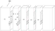
图1a和图1b分别为本发明实施例提供的光束扩展结构的结构示意图;1a and FIG. 1b are respectively schematic structural diagrams of a beam expansion structure provided by an embodiment of the present invention;
图2为本发明实施例提供的光束扩展结构的设计原理示意图;2 is a schematic diagram of a design principle of a beam expansion structure provided by an embodiment of the present invention;
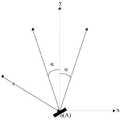
图3为MEMS微镜出射扫描光束的示意图;3 is a schematic diagram of a MEMS micromirror exiting a scanning beam;
图4为本发明实施例提供的光学显示模组的结构示意图。FIG. 4 is a schematic structural diagram of an optical display module provided by an embodiment of the present invention.
具体实施方式Detailed ways
下面结合附图,对本发明实施例提供的光束扩展结构及光学显示模组的具体实施方式进行详细的说明。需要说明的是,本文所描述的实施例仅仅是本发明一部分实施例,而不是全部的实施例。基于本发明中的实施例,本领域普通技术人员在没有做出创造性劳动前提下所获得的所有其他实施例,都属于本发明保护的范围。The specific implementations of the beam expansion structure and the optical display module provided by the embodiments of the present invention will be described in detail below with reference to the accompanying drawings. It should be noted that the embodiments described herein are only a part of the embodiments of the present invention, but not all of the embodiments. Based on the embodiments of the present invention, all other embodiments obtained by those of ordinary skill in the art without creative efforts shall fall within the protection scope of the present invention.
具体地,本发明实施例提供的光束扩展结构,如图1a和图1b所示,包括:多个按序设置且层叠排列的透明基板001,各透明基板001分别包括具有反射功能的第一区域101,以及具有反射透射功能的第二区域102;Specifically, the beam expansion structure provided by the embodiment of the present invention, as shown in FIG. 1a and FIG. 1b, includes: a plurality of
并且,如图2所示,在前设置的各透明基板001的第一区域101,用于将入射光束反射至在后设置的各透明基板001的第二区域102;And, as shown in FIG. 2 , the
在后设置的各透明基板001的第二区域102,用于将接收到的部分入射光束透射至观测基点B所在区域,以及将接收到的其余部分入射光束反射至在前设置的各透明基板001的第二区域102;The
在前设置的各透明基板001的第二区域102,用于将接收到的经在后设置的各所述透明基板的第二区域反射的入射光束部分反射至在后设置的各透明基板001的第二区域102。The
值得注意的是,本发明实施例中的在前设置和在后设置是指各透明基板001之间的相对位置,例如按序设置的第一个透明基板001相对于按序设置的第二个透明基板001则为在前设置,而按序设置的第二个透明基板001相对于按序设置的第一个透明基板001则为在后设置。It should be noted that the preceding arrangement and the succeeding arrangement in the embodiment of the present invention refer to the relative positions between the
并且,由于各透明基板001的第二区域102同时具有反射功能和透射功能,因此,只要入射光线照射至各透明基板001的第二区域102,即可在其上发生透射和反射。Moreover, since the
在本发明实施例提供的上述光束扩展结构中,通过在前设置的各透明基板001的第一区域101将入射光束反射至在后设置的各透明基板001的第二区域102;并通过在后设置的各透明基板001的第二区域102与在前设置的各透明基板001的第二区域102相互配合实现对入射光束的扩展。且在实际应用时可采用MEMS微镜出射的扫描光束作为入射光束;具体地,如图3所示为MEMS微镜出射的扫描光束;MEMS微镜将入射光线s转换成扫描光束,令MEMS微镜的轴心A位于坐标原点o的位置,MEMS微镜在xoy平面内的扫描光束位于y轴两侧α度范围内。基于上述光束扩展结构,将扩展光束后的MEMS微镜与层叠阵列波导结构结合,有利于实现光学显示模组的轻薄化和紧凑化。In the above-mentioned beam expansion structure provided by the embodiment of the present invention, the incident light beam is reflected to the
需要说明的是,在本发明实施例提供的上述光束扩展结构中,每个透明基板001上的第一区域101和第二区域102不仅可以同时位于透明基板001的同一侧,还可以分别设置在透明基板001相对的两侧,在此不做限定。It should be noted that, in the above-mentioned beam expansion structure provided in the embodiment of the present invention, the
另外,为便于描述每个透明基板001上的第一区域101和第二区域102,图1b所示为光束扩展结构中各透明基板001贴合前的示意图。在实际应用时,各透明基板001之间紧密贴合。In addition, in order to facilitate the description of the
在具体实施时,为最大化地实现对入射光束的扩展,在本发明实施例提供的上述光束扩展结构中,入射光束的每一部分分别在对应的透明基板001的第一区域101上实现反射,即入射光束的每一部分分别与各透明基板001的第一区域101一一对应,并在对应的透明基板001的第一区域101上发生反射。较佳地,为了便于设计光束扩展结构,在本发明实施例提供的上述光束扩展结构中,各透明基板001的第一区域101分别对应入射光束的各部分的起止边界光线之间的夹角度数相等。当然,在具体实施时,各透明基板001的第一区域101对应的入射光束的各部分的起止边界光线之间的夹角度数也可以不相等,在此不做限定。In specific implementation, in order to maximize the expansion of the incident beam, in the above beam expansion structure provided in the embodiment of the present invention, each part of the incident beam is reflected on the corresponding
在具体实施时,在本发明实施例提供的上述光束扩展结构中,按序设置的第一个透明基板001的第一区域101在与相邻透明基板001之间交界线上的投影为第一线段;In specific implementation, in the above-mentioned beam expansion structure provided by the embodiment of the present invention, the projection of the
第一线段的两个端点分别为入射光束的产生源的中心和观测基点B连线的平行线与第一个透明基板001的第一区域101对应的入射光束的起止边界光线的交点。具体地,若由MEMS微镜出射的扫描光束作为入射光束,则入射光束的产生源的中心为MEMS微镜的轴心A。The two end points of the first line segment are the intersection points of the parallel line connecting the center of the incident beam generating source and the observation base point B and the starting and ending boundary rays of the incident beam corresponding to the
并且,按序设置的第K个透明基板001的第一区域101在与相邻透明基板001之间交界线上的投影为第K线段,其中,K为大于或等于2的整数;And, the projection of the
第K线段的第一端点为前一透明基板001的第一区域101对应入射光束起始边界光线的反射光线与第K个透明基板001的第一区域101对应的入射光束的终止边界光线的交点,第K线段的第二端点为过第一端点且与第一线段平行的直线与第K个透明基板001的第一区域101对应的入射光束的起始边界光线的交点。The first endpoint of the K-th line segment is the difference between the reflected ray of the
有鉴于此,在本发明实施例提供的上述光束扩展结构中,若各透明基板001面向入射光束一侧的表面上具有第一区域101和第二区域102;In view of this, in the above-mentioned beam expansion structure provided by the embodiment of the present invention, if each
则第K个透明基板的厚度等于第K线段的第一端点与前一透明基板001的第一区域101之间的距离;具体地,第K个透明基板的厚度等于第K线段的第一端点与第K-1个透明基板001的第一区域101对应的第K-1线段之间的垂直距离。Then the thickness of the Kth transparent substrate is equal to the distance between the first end point of the Kth line segment and the
在具体实施时,在本发明实施例提供的上述光束扩展结构中,可以在各透明基板001的第一区域101设置反射功能膜;在各透明基板001的第二区域102设置反射透射功能膜,以实现各透明基板001的第一区域101和第二区域102相应的功能。In specific implementation, in the above-mentioned beam expansion structure provided by the embodiment of the present invention, a reflective functional film may be provided in the
相应地,在本发明实施例提供的上述光束扩展结构中,相邻两个反射功能膜之间的距离与位于相邻两个反射功能膜之间的透明基板001的厚度相等;相邻两个反射透射功能膜之间的距离与位于相邻两个反射透射功能膜之间的透明基板001的厚度相等。Correspondingly, in the above-mentioned beam expansion structure provided by the embodiment of the present invention, the distance between two adjacent reflective functional films is equal to the thickness of the
在具体实施时,为了使入射光束在各透明基板001的第二区域102上至少发生两次反射,以实现对入射光束的扩展,在本发明实施例提供的上述光束扩展结构中,每个透明基板001的第二区域102在与相邻透明基板001之间交界线上的投影长度至少为第一区域101在与相邻透明基板001之间交界线上投影长度的四倍。In a specific implementation, in order to make the incident light beam reflect at least twice on the
在具体实施时,在本发明实施例提供的上述光束扩展结构中,每个透明基板001的第一区域101和第二区域102相互接触,这样设置,使得入射光束的全部光线均可以通过透明基板001的第二区域102进行扩展。During specific implementation, in the above-mentioned beam expansion structure provided by the embodiment of the present invention, the
在具体实施时,在本发明实施例提供的上述光束扩展结构中,透明基板001可以为玻璃基板。当然,透明基板001还可以为本领域技术人员公知的其他具有透光效果良好的基板。例如塑料基板,在此不做限定。During specific implementation, in the above-mentioned beam expansion structure provided by the embodiment of the present invention, the
为了更好地说明本发明的技术方案,下面以MEMS微镜出射的扫描光束作为入射光束为例,对本发明实施例提供的上述光束扩展结构的设计原理及具体实现方式进行详细说明。In order to better illustrate the technical solution of the present invention, the following takes the scanning beam emitted by the MEMS micromirror as the incident beam as an example to describe in detail the design principle and specific implementation of the above beam expansion structure provided by the embodiment of the present invention.
具体地,本发明实施例提供的上述光束扩展结构的设计原理如图2所示。以将MEMS微镜的扫描光束依次划分为5个子扫描光束,每个子扫描光束的扫描范围相等均为β度,并设定各子扫描光束的边界分别为光线i1、i2、i3、i4、i5和i6为例。Specifically, the design principle of the above-mentioned beam expansion structure provided by the embodiment of the present invention is shown in FIG. 2 . The scanning beam of the MEMS micromirror is divided into 5 sub-scanning beams in turn, and the scanning range of each sub-scanning beam is equal to β degrees, and the boundaries of each sub-scanning beam are set as rays i1, i2, i3, i4, i5 and i6 for example.
具体地,如图2所示,首先确定光线i1和光线i2围合形成的子扫描光束对应的第一线段M1的位置,具体如下:Specifically, as shown in FIG. 2, first determine the position of the first line segment M1 corresponding to the sub-scanning beam formed by the ray i1 and the ray i2, as follows:
确定MEMS微镜的轴心A与观察基点B所在位置;Determine the position of the axis A of the MEMS micromirror and the observation base point B;
构造MEMS微镜的轴心A与观察基点B连线L1的垂直平分线L2;Construct the vertical bisector L2 of the line L1 connecting the axis A of the MEMS micromirror and the observation base point B;
确定垂直平分线L2与光线i2的交点t1;Determine the intersection t1 of the vertical bisector L2 and the ray i2;
以交点t1为垂足,作垂直于垂直平分线L2的直线,使直线与光线i1相交于点b1;Taking the intersection point t1 as the vertical foot, draw a straight line perpendicular to the vertical bisector L2, so that the straight line and the ray i1 intersect at the point b1;
交点b1与交点t1即为第一线段M1的两个端点。The intersection b1 and the intersection t1 are the two endpoints of the first line segment M1.
进一步地,确定光线i2和光线i3围合形成的子扫描光束对应的第二线段M2的位置:Further, determine the position of the second line segment M2 corresponding to the sub-scanning beam formed by the ray i2 and the ray i3:
确定光线i1经主反射区M1反射的光线r1与光线i3的交点t2;Determine the intersection t2 of the ray r1 reflected by the main reflection area M1 and the ray i3 of the ray i1;
过交点t2作垂直平分线L2的垂线,使垂线与光线i2相交于点b2;Make the vertical line of the vertical bisector L2 through the intersection point t2, so that the vertical line and the ray i2 intersect at the point b2;
交点b2与交点t2即为第二线段M2的两个端点。可以看出第二线段M2与第一线段M1平行。The intersection point b2 and the intersection point t2 are the two end points of the second line segment M2. It can be seen that the second line segment M2 is parallel to the first line segment M1.
之后,采用确定第二线段M2位置的类似方法,确定光线i2和光线i3、光线i3和光线i4、光线i4和光线i5分别围合形成的子扫描光束对应的各线段的位置。Afterwards, a similar method for determining the position of the second line segment M2 is used to determine the positions of the respective line segments corresponding to the sub-scanning beams formed by ray i2 and ray i3, ray i3 and ray i4, and ray i4 and ray i5 respectively.
将与上述5个子扫描光束一一对应的透明基板001分别标记为G1、G2、G3、G4和G5,如图1a所示,则确定第一线段M1为G1的第一区域101在与G2的交界线j1上的正投影;第二线段M2为G2的第一区域101在与G3的交界线j2上的正投影;类似可确定G3的第一区域101、G4的第一区域101和G5的第一区域101分别在与相邻透明基板001的交界线上的正投影。The
自各子扫描光束分别对应的各线段邻近垂直平分线L1的一端至少延伸各线段长度的四倍,以使各子扫描光束可以在各透明基板001的第二区域上至少发生两次反射,并且所得延伸部分的延伸线段即为各透明基板001的第二区域102在与相邻透明基板001的交界线上的正投影。例如,自端点t1延伸第一线段M1至延伸部分长度至少为第一线段M1长度的四倍,并且延伸部分的延伸线段m1即为G1的第二区域102与G2的交界线j1上的正投影;图2示出了光线i2在延伸线段m1上发生两次反射的光路图。From one end of each line segment corresponding to each sub-scanning beam adjacent to the vertical bisector L1 at least four times the length of each line segment, so that each sub-scanning beam can be reflected at least twice on the second area of each
在第一线段M1对应G1的第一区域101上设置反射功能膜,并在延伸线段m1对应G1的第二区域102上设置反射透射功能膜。A reflective functional film is provided on the
选择厚度h等于第一线段M1与第二线段M2之间距离的G2,如图1b所示;并基于实现G1的反射功能膜与反射透射功能膜的类似方法,分别实现G2、G3、G4和G5的反射功能膜与反射透射功能膜。Select G2 whose thickness h is equal to the distance between the first line segment M1 and the second line segment M2, as shown in Figure 1b; and based on the similar method of realizing the reflective functional film and the reflective and transmissive functional film of G1, G2, G3, G4 are respectively realized And G5's reflective functional film and reflective and transmissive functional film.
将各透明基板001按照G1、G2、G3、G4、G5的顺序依次黏贴在一起,并使各透明基板001具有功能膜的表面朝向同一侧。此时,相邻两个反射功能膜之间的距离就等于二者之间透明基板001的厚度,例如,第一线段M1对应的反射功能膜与第二线段M2对应的反射功能膜之间的距离等于G2的厚度h;同样,相邻两个反射透射功能膜之间的距离也等于二者之间透明基板001的厚度,例如,第一线段M1的延伸线段m1对应的反射透射功能膜与第二线段M2的延伸线段m2对应的反射透射功能膜之间的距离等于G2的厚度h。The
基于同一发明构思,本发明实施例提供了一种光学显示模组,如图4所示,包括上述光束扩展结构401,激光光源(图中未示出),微机电系统MEMS微镜402,以及层叠阵列波导结构403;其中,Based on the same inventive concept, an embodiment of the present invention provides an optical display module, as shown in FIG. 4 , including the above-mentioned
MEMS微镜402,用于将激光光源发出的光线转化为具有图像信息的扫描光束,并将扫描光束出射至光束扩展结构;The MEMS micromirror 402 is used to convert the light emitted by the laser light source into a scanning beam with image information, and output the scanning beam to the beam expansion structure;
光束扩展结构401,用于在第一维方向上扩展接收到的扫描光束,并将扩展后的扫描光束汇聚至层叠阵列波导结构403;具体地,光束扩展结构401在x-y平面内扩展扫描光束;The
层叠阵列波导结构403,用于将接收到的扫描光束在第二维方向上扩展出瞳;具体地,层叠阵列波导结构403在x-z平面内扩展扫描光束。The stacked arrayed
由上述描述可知,采用光束扩展结构401与层叠阵列波导结构403可共同完成扫描光束在二维方向上的扩展,达到对MEMS微镜出射细光束扩展的目的,从而利于观察者观察。It can be seen from the above description that the
在具体实施时,为了减小MEMS微镜402与光束扩展结构401之间的距离,在本发明实施例提供的上述光学显示模组中,如图4所示,还可以包括:位于MEMS微镜402与光束扩展结构401之间光路上的反射镜404;During specific implementation, in order to reduce the distance between the
反射镜404,用于将扫描光束反射至光束扩展结构401。The
本发明实施例提供的上述光束扩展结构及光学显示模组,包括:多个按序设置且层叠排列的透明基板,各透明基板分别包括具有反射功能的第一区域和具有反射透射功能的第二区域;通过在前设置的各透明基板的第一区域将入射光束反射至在后设置的各透明基板的第二区域;并通过在后设置的各透明基板的第二区域与在前设置的各透明基板的第二区域相互配合实现对入射光束的扩展,且在实际应用时,可采用MEMS微镜出射的扫描光束作为入射光束,从而有利于实现MEMS微镜与层叠阵列波导结构的结合,进而实现光学显示模组的轻薄化和紧凑化。The above-mentioned beam expansion structure and optical display module provided by the embodiment of the present invention include: a plurality of transparent substrates arranged in sequence and arranged in layers, and each transparent substrate respectively includes a first area with a reflective function and a second area with a reflective and transmissive function. area; the incident light beam is reflected to the second area of each transparent substrate arranged afterward through the first area of each transparent substrate arranged in front; and the second area of each transparent substrate arranged after and each The second area of the transparent substrate cooperates with each other to expand the incident beam, and in practical applications, the scanning beam emitted by the MEMS micromirror can be used as the incident beam, which is conducive to realizing the combination of the MEMS micromirror and the laminated array waveguide structure, and then Realize the thinning and compactness of the optical display module.
需要说明的是,在本文中,诸如第一和第二之类的关系术语仅仅用来将一个实体或操作与另一个实体或操作区分开来,而不一定要求或者暗示这些实体或操作之间存在任何这种实际的关系或者顺序。It should be noted that, in this document, relational terms such as first and second are only used to distinguish one entity or operation from another entity or operation, and do not necessarily require or imply a relationship between these entities or operations. There is no such actual relationship or sequence.
显然,本领域的技术人员可以对本发明进行各种改动和变型而不脱离本发明的精神和范围。这样,倘若本发明的这些修改和变型属于本发明权利要求及其等同技术的范围之内,则本发明也意图包含这些改动和变型在内。It will be apparent to those skilled in the art that various modifications and variations can be made in the present invention without departing from the spirit and scope of the invention. Thus, provided that these modifications and variations of the present invention fall within the scope of the claims of the present invention and their equivalents, the present invention is also intended to include these modifications and variations.
Claims (14)
Priority Applications (2)
| Application Number | Priority Date | Filing Date | Title |
|---|---|---|---|
| CN201710693448.XACN107422474B (en) | 2017-08-14 | 2017-08-14 | A beam expansion structure and optical display module |
| US15/935,146US10598944B2 (en) | 2017-08-14 | 2018-03-26 | Beam expanding structure and optical display module |
Applications Claiming Priority (1)
| Application Number | Priority Date | Filing Date | Title |
|---|---|---|---|
| CN201710693448.XACN107422474B (en) | 2017-08-14 | 2017-08-14 | A beam expansion structure and optical display module |
Publications (2)
| Publication Number | Publication Date |
|---|---|
| CN107422474A CN107422474A (en) | 2017-12-01 |
| CN107422474Btrue CN107422474B (en) | 2020-12-01 |
Family
ID=60436752
Family Applications (1)
| Application Number | Title | Priority Date | Filing Date |
|---|---|---|---|
| CN201710693448.XAActiveCN107422474B (en) | 2017-08-14 | 2017-08-14 | A beam expansion structure and optical display module |
Country Status (2)
| Country | Link |
|---|---|
| US (1) | US10598944B2 (en) |
| CN (1) | CN107422474B (en) |
Families Citing this family (3)
| Publication number | Priority date | Publication date | Assignee | Title |
|---|---|---|---|---|
| JPWO2019111926A1 (en)* | 2017-12-07 | 2020-12-10 | キヤノン株式会社 | Display device and head-mounted display |
| US11892761B2 (en)* | 2019-12-19 | 2024-02-06 | Lumus Ltd. | Image projector using a phase image generator |
| US12124076B2 (en) | 2021-06-29 | 2024-10-22 | Infineon Technologies Ag | Cascaded eyebox expansion in extended reality image projection devices |
Family Cites Families (25)
| Publication number | Priority date | Publication date | Assignee | Title |
|---|---|---|---|---|
| US5724163A (en)* | 1996-11-12 | 1998-03-03 | Yariv Ben-Yehuda | Optical system for alternative or simultaneous direction of light originating from two scenes to the eye of a viewer |
| US6805490B2 (en) | 2002-09-30 | 2004-10-19 | Nokia Corporation | Method and system for beam expansion in a display device |
| JP4404568B2 (en)* | 2003-04-10 | 2010-01-27 | 株式会社エルモ社 | Infrared cut filter and manufacturing method thereof |
| US7573640B2 (en)* | 2005-04-04 | 2009-08-11 | Mirage Innovations Ltd. | Multi-plane optical apparatus |
| CN101243022B (en)* | 2005-08-16 | 2012-07-11 | 旭硝子株式会社 | Infrared reflective glass panels and laminated glass for car windows |
| WO2007020792A1 (en) | 2005-08-16 | 2007-02-22 | Asahi Glass Company, Limited | Infrared reflective glass plate and laminated glass for vehicle window |
| KR101298786B1 (en)* | 2005-08-27 | 2013-08-22 | 쓰리엠 이노베이티브 프로퍼티즈 컴파니 | Illumination assembly and system |
| GB2434877A (en) | 2006-02-06 | 2007-08-08 | Qinetiq Ltd | MOEMS optical modulator |
| WO2009077802A1 (en)* | 2007-12-18 | 2009-06-25 | Nokia Corporation | Exit pupil expanders with wide field-of-view |
| EP2138886A3 (en)* | 2008-06-25 | 2011-10-05 | Samsung Electronics Co., Ltd. | Compact virtual display |
| JP5545076B2 (en) | 2009-07-22 | 2014-07-09 | ソニー株式会社 | Image display device and optical device |
| US8634119B2 (en)* | 2010-07-09 | 2014-01-21 | Tipd, Llc | System for holography |
| EP3309602A1 (en)* | 2011-08-29 | 2018-04-18 | Vuzix Corporation | Controllable waveguide for near-eye display applications |
| CN106125308B (en)* | 2012-04-25 | 2019-10-25 | 罗克韦尔柯林斯公司 | Device and method for displaying images |
| JP6236987B2 (en)* | 2013-08-23 | 2017-11-29 | ミツミ電機株式会社 | Optical scanning device and optical scanning unit |
| US20150205134A1 (en)* | 2014-01-17 | 2015-07-23 | Thalmic Labs Inc. | Systems, articles, and methods for wearable heads-up displays |
| US9519089B1 (en)* | 2014-01-30 | 2016-12-13 | Rockwell Collins, Inc. | High performance volume phase gratings |
| JP6391952B2 (en)* | 2014-03-17 | 2018-09-19 | ソニー株式会社 | Display device and optical device |
| CN203871649U (en)* | 2014-05-09 | 2014-10-08 | 西安炬光科技有限公司 | High-power semiconductor laser beam expanding system |
| US10247943B1 (en)* | 2015-05-18 | 2019-04-02 | Rockwell Collins, Inc. | Head up display (HUD) using a light pipe |
| US10078219B2 (en)* | 2015-05-28 | 2018-09-18 | Thalmic Labs Inc. | Wearable heads-up display with integrated eye tracker and different optical power holograms |
| US10234686B2 (en)* | 2015-11-16 | 2019-03-19 | Microsoft Technology Licensing, Llc | Rainbow removal in near-eye display using polarization-sensitive grating |
| KR102552582B1 (en)* | 2016-03-08 | 2023-07-07 | 삼성디스플레이 주식회사 | Illumination apparatus and holographic display comprising the same |
| US10317679B2 (en)* | 2016-04-04 | 2019-06-11 | Akonia Holographics, Llc | Light homogenization |
| WO2018027326A1 (en)* | 2016-08-12 | 2018-02-15 | Thalmic Labs Inc. | Systems, devices, and methods for variable luminance in wearable heads-up displays |
- 2017
- 2017-08-14CNCN201710693448.XApatent/CN107422474B/enactiveActive
- 2018
- 2018-03-26USUS15/935,146patent/US10598944B2/enactiveActive
Also Published As
| Publication number | Publication date |
|---|---|
| US20190049738A1 (en) | 2019-02-14 |
| US10598944B2 (en) | 2020-03-24 |
| CN107422474A (en) | 2017-12-01 |
Similar Documents
| Publication | Publication Date | Title |
|---|---|---|
| US11579453B2 (en) | Compact beam expanding system | |
| CN101405627B (en) | Imageing element and display | |
| US9651778B2 (en) | Light flux diameter enlarging element and display device | |
| TWM591175U (en) | Compact collimating optical device and system | |
| WO2018157713A1 (en) | Information display device and information display method | |
| CN101680976A (en) | Real mirror video image forming optical system | |
| JP6503693B2 (en) | Optical element, method of manufacturing optical element, optical device and display device | |
| CN107422474B (en) | A beam expansion structure and optical display module | |
| CN111273261B (en) | Coaxial transmitting and receiving laser radar based on off-axis incidence | |
| CN103827745B (en) | Optical system with compact back focus | |
| WO1997001116A1 (en) | Optical image formation apparatus | |
| US8888290B2 (en) | Polarization beam splitters for image projection apparatus | |
| JP7664288B2 (en) | Three-dimensional display device | |
| JP6507575B2 (en) | Optical device and display device | |
| TW201627744A (en) | Projector | |
| CN102156354B (en) | Stereo-projection system | |
| CN112462564B (en) | Laser optical projection module and wearable device comprising same | |
| US10281655B2 (en) | Field inversion waveguide using micro-prism array | |
| CN218728138U (en) | Optical waveguide device and near-to-eye display device | |
| CN116338964B (en) | Head-up display module assembly and carrier | |
| TWI891024B (en) | Holographic projection operating device, holographic projection device and holographic optical module thereof | |
| CN112882229A (en) | Augmented reality display system | |
| TWI848278B (en) | Holographic projection operating device, holographic projection device and holographic optical module thereof | |
| US20220244537A1 (en) | Optical assembly and head-mounted apparatus | |
| TWM632144U (en) | Holographic projection operating device, holographic projection device and holographic optical module thereof |
Legal Events
| Date | Code | Title | Description |
|---|---|---|---|
| PB01 | Publication | ||
| PB01 | Publication | ||
| SE01 | Entry into force of request for substantive examination | ||
| GR01 | Patent grant | ||
| GR01 | Patent grant |