CN107406966B - Oxide semiconductor film, semiconductor device including the oxide semiconductor film, and display device including the semiconductor device - Google Patents
Oxide semiconductor film, semiconductor device including the oxide semiconductor film, and display device including the semiconductor deviceDownload PDFInfo
- Publication number
- CN107406966B CN107406966BCN201680013345.8ACN201680013345ACN107406966BCN 107406966 BCN107406966 BCN 107406966BCN 201680013345 ACN201680013345 ACN 201680013345ACN 107406966 BCN107406966 BCN 107406966B
- Authority
- CN
- China
- Prior art keywords
- film
- oxide semiconductor
- semiconductor film
- substrate
- insulating film
- Prior art date
- Legal status (The legal status is an assumption and is not a legal conclusion. Google has not performed a legal analysis and makes no representation as to the accuracy of the status listed.)
- Active
Links
Images


Classifications
- H—ELECTRICITY
- H10—SEMICONDUCTOR DEVICES; ELECTRIC SOLID-STATE DEVICES NOT OTHERWISE PROVIDED FOR
- H10D—INORGANIC ELECTRIC SEMICONDUCTOR DEVICES
- H10D30/00—Field-effect transistors [FET]
- H10D30/60—Insulated-gate field-effect transistors [IGFET]
- H10D30/67—Thin-film transistors [TFT]
- H10D30/674—Thin-film transistors [TFT] characterised by the active materials
- H10D30/6755—Oxide semiconductors, e.g. zinc oxide, copper aluminium oxide or cadmium stannate
- H—ELECTRICITY
- H10—SEMICONDUCTOR DEVICES; ELECTRIC SOLID-STATE DEVICES NOT OTHERWISE PROVIDED FOR
- H10D—INORGANIC ELECTRIC SEMICONDUCTOR DEVICES
- H10D30/00—Field-effect transistors [FET]
- H10D30/60—Insulated-gate field-effect transistors [IGFET]
- H10D30/67—Thin-film transistors [TFT]
- H10D30/6729—Thin-film transistors [TFT] characterised by the electrodes
- H10D30/673—Thin-film transistors [TFT] characterised by the electrodes characterised by the shapes, relative sizes or dispositions of the gate electrodes
- H10D30/6733—Multi-gate TFTs
- H10D30/6734—Multi-gate TFTs having gate electrodes arranged on both top and bottom sides of the channel, e.g. dual-gate TFTs
- H—ELECTRICITY
- H10—SEMICONDUCTOR DEVICES; ELECTRIC SOLID-STATE DEVICES NOT OTHERWISE PROVIDED FOR
- H10D—INORGANIC ELECTRIC SEMICONDUCTOR DEVICES
- H10D30/00—Field-effect transistors [FET]
- H10D30/60—Insulated-gate field-effect transistors [IGFET]
- H10D30/67—Thin-film transistors [TFT]
- H10D30/6729—Thin-film transistors [TFT] characterised by the electrodes
- H10D30/6737—Thin-film transistors [TFT] characterised by the electrodes characterised by the electrode materials
- H10D30/6739—Conductor-insulator-semiconductor electrodes
- H—ELECTRICITY
- H10—SEMICONDUCTOR DEVICES; ELECTRIC SOLID-STATE DEVICES NOT OTHERWISE PROVIDED FOR
- H10D—INORGANIC ELECTRIC SEMICONDUCTOR DEVICES
- H10D30/00—Field-effect transistors [FET]
- H10D30/60—Insulated-gate field-effect transistors [IGFET]
- H10D30/67—Thin-film transistors [TFT]
- H10D30/674—Thin-film transistors [TFT] characterised by the active materials
- H10D30/6755—Oxide semiconductors, e.g. zinc oxide, copper aluminium oxide or cadmium stannate
- H10D30/6756—Amorphous oxide semiconductors
- H—ELECTRICITY
- H10—SEMICONDUCTOR DEVICES; ELECTRIC SOLID-STATE DEVICES NOT OTHERWISE PROVIDED FOR
- H10D—INORGANIC ELECTRIC SEMICONDUCTOR DEVICES
- H10D30/00—Field-effect transistors [FET]
- H10D30/60—Insulated-gate field-effect transistors [IGFET]
- H10D30/67—Thin-film transistors [TFT]
- H10D30/6757—Thin-film transistors [TFT] characterised by the structure of the channel, e.g. transverse or longitudinal shape or doping profile
- H—ELECTRICITY
- H10—SEMICONDUCTOR DEVICES; ELECTRIC SOLID-STATE DEVICES NOT OTHERWISE PROVIDED FOR
- H10D—INORGANIC ELECTRIC SEMICONDUCTOR DEVICES
- H10D62/00—Semiconductor bodies, or regions thereof, of devices having potential barriers
- H10D62/40—Crystalline structures
- H10D62/405—Orientations of crystalline planes
- H—ELECTRICITY
- H10—SEMICONDUCTOR DEVICES; ELECTRIC SOLID-STATE DEVICES NOT OTHERWISE PROVIDED FOR
- H10D—INORGANIC ELECTRIC SEMICONDUCTOR DEVICES
- H10D62/00—Semiconductor bodies, or regions thereof, of devices having potential barriers
- H10D62/50—Physical imperfections
- H10D62/57—Physical imperfections the imperfections being on the surface of the semiconductor body, e.g. the body having a roughened surface
- H—ELECTRICITY
- H10—SEMICONDUCTOR DEVICES; ELECTRIC SOLID-STATE DEVICES NOT OTHERWISE PROVIDED FOR
- H10D—INORGANIC ELECTRIC SEMICONDUCTOR DEVICES
- H10D62/00—Semiconductor bodies, or regions thereof, of devices having potential barriers
- H10D62/80—Semiconductor bodies, or regions thereof, of devices having potential barriers characterised by the materials
- H—ELECTRICITY
- H10—SEMICONDUCTOR DEVICES; ELECTRIC SOLID-STATE DEVICES NOT OTHERWISE PROVIDED FOR
- H10D—INORGANIC ELECTRIC SEMICONDUCTOR DEVICES
- H10D86/00—Integrated devices formed in or on insulating or conducting substrates, e.g. formed in silicon-on-insulator [SOI] substrates or on stainless steel or glass substrates
- H10D86/40—Integrated devices formed in or on insulating or conducting substrates, e.g. formed in silicon-on-insulator [SOI] substrates or on stainless steel or glass substrates characterised by multiple TFTs
- H10D86/421—Integrated devices formed in or on insulating or conducting substrates, e.g. formed in silicon-on-insulator [SOI] substrates or on stainless steel or glass substrates characterised by multiple TFTs having a particular composition, shape or crystalline structure of the active layer
- H10D86/423—Integrated devices formed in or on insulating or conducting substrates, e.g. formed in silicon-on-insulator [SOI] substrates or on stainless steel or glass substrates characterised by multiple TFTs having a particular composition, shape or crystalline structure of the active layer comprising semiconductor materials not belonging to the Group IV, e.g. InGaZnO
- H—ELECTRICITY
- H10—SEMICONDUCTOR DEVICES; ELECTRIC SOLID-STATE DEVICES NOT OTHERWISE PROVIDED FOR
- H10D—INORGANIC ELECTRIC SEMICONDUCTOR DEVICES
- H10D86/00—Integrated devices formed in or on insulating or conducting substrates, e.g. formed in silicon-on-insulator [SOI] substrates or on stainless steel or glass substrates
- H10D86/40—Integrated devices formed in or on insulating or conducting substrates, e.g. formed in silicon-on-insulator [SOI] substrates or on stainless steel or glass substrates characterised by multiple TFTs
- H10D86/451—Integrated devices formed in or on insulating or conducting substrates, e.g. formed in silicon-on-insulator [SOI] substrates or on stainless steel or glass substrates characterised by multiple TFTs characterised by the compositions or shapes of the interlayer dielectrics
- H—ELECTRICITY
- H10—SEMICONDUCTOR DEVICES; ELECTRIC SOLID-STATE DEVICES NOT OTHERWISE PROVIDED FOR
- H10D—INORGANIC ELECTRIC SEMICONDUCTOR DEVICES
- H10D86/00—Integrated devices formed in or on insulating or conducting substrates, e.g. formed in silicon-on-insulator [SOI] substrates or on stainless steel or glass substrates
- H10D86/40—Integrated devices formed in or on insulating or conducting substrates, e.g. formed in silicon-on-insulator [SOI] substrates or on stainless steel or glass substrates characterised by multiple TFTs
- H10D86/60—Integrated devices formed in or on insulating or conducting substrates, e.g. formed in silicon-on-insulator [SOI] substrates or on stainless steel or glass substrates characterised by multiple TFTs wherein the TFTs are in active matrices
- H—ELECTRICITY
- H10—SEMICONDUCTOR DEVICES; ELECTRIC SOLID-STATE DEVICES NOT OTHERWISE PROVIDED FOR
- H10D—INORGANIC ELECTRIC SEMICONDUCTOR DEVICES
- H10D99/00—Subject matter not provided for in other groups of this subclass
Landscapes
- Thin Film Transistor (AREA)
- Physical Vapour Deposition (AREA)
- Physical Deposition Of Substances That Are Components Of Semiconductor Devices (AREA)
Abstract
Description
Translated fromChinese技术领域technical field
本发明的一个方式涉及一种氧化物半导体膜、包括该氧化物半导体膜的半导体装置以及包括该半导体装置的显示装置。One aspect of the present invention relates to an oxide semiconductor film, a semiconductor device including the oxide semiconductor film, and a display device including the semiconductor device.
注意,本发明的一个方式不局限于上述技术领域。本说明书等所公开的发明的一个方式的技术领域涉及一种物体、方法或制造方法。另外,本发明的一个方式涉及一种工序(process)、机器(machine)、产品(manufacture)或者组合物(composition of matter)。具体而言,本说明书所公开的本发明的一个方式的技术领域的例子包括:半导体装置、显示装置、液晶显示装置、发光装置、照明装置、蓄电装置、存储装置、摄像装置、这些装置的驱动方法以及这些装置的制造方法。Note that one form of the present invention is not limited to the above-mentioned technical field. The technical field of one aspect of the invention disclosed in this specification and the like relates to an object, a method, or a manufacturing method. Moreover, one form of this invention relates to a process (process), machine (machine), product (manufacture) or composition (composition of matter). Specifically, examples of the technical field of one embodiment of the present invention disclosed in this specification include semiconductor devices, display devices, liquid crystal display devices, light-emitting devices, lighting devices, power storage devices, storage devices, imaging devices, and the like. A method of driving and a method of manufacturing these devices.
在本说明书等中,半导体装置是指能够通过利用半导体特性而工作的所有装置。晶体管等半导体元件、半导体电路、运算装置及存储装置是半导体装置的一个方式。摄像装置、显示装置、液晶显示装置、发光装置、电光装置、发电装置(包括薄膜太阳能电池及有机薄膜太阳能电池等)及电子设备有时包括半导体装置。In this specification and the like, a semiconductor device refers to all devices that can operate by utilizing semiconductor characteristics. Semiconductor elements such as transistors, semiconductor circuits, arithmetic devices, and storage devices are one form of semiconductor devices. Image pickup devices, display devices, liquid crystal display devices, light-emitting devices, electro-optical devices, power generation devices (including thin-film solar cells, organic thin-film solar cells, etc.), and electronic equipment sometimes include semiconductor devices.
背景技术Background technique
通过使用形成在衬底上的半导体薄膜来形成晶体管(薄膜晶体管(TFT)或场效应晶体管(FET))的技术受到关注。该晶体管被广泛地应用于如集成电路(IC)及图像装置(显示装置)等电子器件。作为可以应用于晶体管的半导体薄膜,硅类半导体材料被宽泛地使用,但是作为其他材料,氧化物半导体受到注目。A technique of forming a transistor (thin film transistor (TFT) or field effect transistor (FET)) by using a semiconductor thin film formed on a substrate is attracting attention. This transistor is widely used in electronic devices such as integrated circuits (ICs) and image devices (display devices). Silicon-based semiconductor materials are widely used as semiconductor thin films that can be applied to transistors, but oxide semiconductors are attracting attention as other materials.
例如,已公开了使用In-Ga-Zn类氧化物半导体制造晶体管的技术(参照专利文献1)。For example, a technique of manufacturing a transistor using an In-Ga-Zn-based oxide semiconductor has been disclosed (refer to Patent Document 1).
[参考文献][references]
[专利文献][Patent Literature]
[专利文献1]日本专利申请公开第2007-96055号公报[Patent Document 1] Japanese Patent Application Laid-Open No. 2007-96055
发明内容SUMMARY OF THE INVENTION
本发明的一个方式的目的是提供一种新颖的氧化物半导体膜。本发明的一个方式的其他目的是提供一种缺陷少的氧化物半导体膜。本发明的一个方式的其他目的是提供一种氧化物半导体膜与绝缘膜的界面的浅缺陷态密度的峰值小的氧化物半导体膜。本发明的一个方式的其他目的是提供一种包括电特性(例如,通态电流、场效应迁移率、频率特性)优良的晶体管的半导体装置。本发明的一个方式的其他目的是提供一种包括饱和性优良的晶体管的半导体装置。本发明的一个方式的其他目的是提供一种包括可靠性高的晶体管的半导体装置。本发明的一个方式的其他目的是提供一种新颖的半导体装置。本发明的一个方式的其他目的是提供一种新颖的半导体装置的制造方法。An object of one embodiment of the present invention is to provide a novel oxide semiconductor film. Another object of one embodiment of the present invention is to provide an oxide semiconductor film with few defects. Another object of one embodiment of the present invention is to provide an oxide semiconductor film with a small peak of the shallow defect state density at the interface between the oxide semiconductor film and the insulating film. Another object of one embodiment of the present invention is to provide a semiconductor device including a transistor having excellent electrical characteristics (eg, on-state current, field-effect mobility, and frequency characteristics). Another object of one embodiment of the present invention is to provide a semiconductor device including a transistor excellent in saturation. Another object of one embodiment of the present invention is to provide a semiconductor device including a highly reliable transistor. Another object of one embodiment of the present invention is to provide a novel semiconductor device. Another object of one embodiment of the present invention is to provide a novel manufacturing method of a semiconductor device.
注意,上述目的的记载不妨碍其他目的的存在。在本发明的一个方式中并不需要实现所有上述目的。上述目的以外的目的从说明书等的记载看来是显而易见的,并可以从说明书等中抽取上述目的以外的目的。Note that the description of the above purpose does not prevent the existence of other purposes. Not all of the above objects need to be achieved in one form of the present invention. Objects other than the above-mentioned objects are obvious from the description in the specification and the like, and objects other than the above-mentioned objects can be extracted from the specification and the like.
本发明的一个方式是一种氧化物半导体膜,包括:In;M(M是Al、Ga、Y或Sn);Zn;以及浅缺陷态密度的峰值小于1×1013cm-2eV-1的区域。One embodiment of the present invention is an oxide semiconductor film comprising: In; M (M is Al, Ga, Y, or Sn); Zn; and a shallow defect state density with a peak value of less than 1×1013 cm-2 eV-1 Area.
本发明的另一个方式是一种氧化物半导体膜,包括:In;M(M是Al、Ga、Y或Sn);Zn;以及隔着第一绝缘膜重叠于第一导电膜的第一区域。第一区域包括氧化物半导体膜与第一绝缘膜的界面的浅缺陷态密度的峰值小于1×1013cm-2eV-1的区域。Another aspect of the present invention is an oxide semiconductor film including: In; M (M is Al, Ga, Y, or Sn); Zn; and a first region overlapping a first conductive film via a first insulating film . The first region includes a region where the peak value of the shallow defect state density at the interface of the oxide semiconductor film and the first insulating film is less than 1×1013 cm−2 eV−1 .
在上述各方式中,浅缺陷态密度的峰值优选通过高频C-V法测量。In each of the above methods, the peak value of the shallow defect state density is preferably measured by the high-frequency C-V method.
在上述方式中,优选的是,浅缺陷态密度的峰值通过高频C-V法测量,并且在高频C-V法中对第一导电膜施加直流电压和0.1kHz以上且10MHz以下的交流电压。In the above-mentioned form, it is preferable that the peak value of the shallow defect state density is measured by the high-frequency C-V method, and that a DC voltage and an AC voltage of 0.1 kHz or more and 10 MHz or less are applied to the first conductive film in the high-frequency C-V method.
本发明的另一个方式是一种氧化物半导体膜,包括:In;M(M表示Al、Ga、Y或Sn);Zn;隔着第一绝缘膜重叠于第一导电膜的第一区域;以及隔着第二绝缘膜重叠于第二导电膜的第二区域。第一区域包括氧化物半导体膜与第一绝缘膜的界面的第一浅缺陷态密度的峰值小于1×1013cm-2eV-1的区域。第二区域包括氧化物半导体膜与第二绝缘膜的界面的第二浅缺陷态密度的峰值小于1×1013cm-2eV-1的区域。Another aspect of the present invention is an oxide semiconductor film, comprising: In; M (M represents Al, Ga, Y, or Sn); Zn; a first region overlapping the first conductive film via a first insulating film; and a second region overlapping the second conductive film via the second insulating film. The first region includes a region where the peak value of the first shallow defect state density at the interface of the oxide semiconductor film and the first insulating film is less than 1×1013 cm−2 eV−1 . The second region includes a region where the peak value of the second shallow defect state density at the interface of the oxide semiconductor film and the second insulating film is less than 1×1013 cm−2 eV−1 .
在上述方式中,优选包括第一浅缺陷态密度的峰值大致与第二浅缺陷态密度的峰值一致的区域。In the above-described form, it is preferable to include a region in which the peak of the first shallow defect state density substantially coincides with the peak of the second shallow defect state density.
在上述各方式中,第一浅缺陷态密度的峰值及第二浅缺陷态密度的峰值优选通过高频C-V法测量。In each of the above-described methods, the peak value of the first shallow defect state density and the peak value of the second shallow defect state density are preferably measured by a high-frequency C-V method.
在上述方式的高频C-V法中,优选对第一导电膜或第二导电膜施加0.1kHz以上且10MHz以下的交流电压和直流电压。In the high-frequency C-V method of the above aspect, it is preferable to apply an AC voltage and a DC voltage of 0.1 kHz or more and 10 MHz or less to the first conductive film or the second conductive film.
在上述各方式中,氧化物半导体膜优选包括具有c轴取向性的区域。In each of the above aspects, the oxide semiconductor film preferably includes a region having c-axis orientation.
本发明的另一个方式是一种半导体装置,包括:上述各方式的氧化物半导体膜;与氧化物半导体膜电连接的源电极;以及与氧化物半导体膜电连接的漏电极。Another aspect of the present invention is a semiconductor device including: the oxide semiconductor film of each aspect described above; a source electrode electrically connected to the oxide semiconductor film; and a drain electrode electrically connected to the oxide semiconductor film.
本发明的另一个方式是一种包括上述各方式的氧化物半导体膜的半导体装置。在第一绝缘膜中通过热脱附谱分析法检测出1×1014cm-2以下的氩分子。Another aspect of the present invention is a semiconductor device including the oxide semiconductor film of each aspect described above. In the first insulating film, argon molecules of 1×1014 cm−2 or less were detected by thermal desorption spectroscopy.
本发明的另一个方式是一种包括上述各方式的氧化物半导体膜的半导体装置。在第一绝缘膜中通过热脱附谱分析法检测出1×1015cm-2以下的氧分子。Another aspect of the present invention is a semiconductor device including the oxide semiconductor film of each aspect described above. In the first insulating film, oxygen molecules of 1×1015 cm−2 or less were detected by thermal desorption spectroscopy.
本发明的另一个方式是一种显示装置,包括:上述各方式的半导体装置;以及显示元件。本发明的另一个方式是一种显示模块,包括:上述方式的显示装置;以及触摸传感器。本发明的另一个方式是一种电子设备,包括:上述各方式的半导体装置、上述方式的显示装置或上述方式的显示模块;以及操作键或电池。Another aspect of the present invention is a display device including: the semiconductor device of each aspect described above; and a display element. Another aspect of the present invention is a display module, including: the display device of the aforementioned aspect; and a touch sensor. Another aspect of the present invention is an electronic device including: the semiconductor device of each of the aforementioned aspects, the display device of the aforementioned aspect, or the display module of the aforementioned aspect; and an operation key or a battery.
根据本发明的一个方式,可以提供一种新颖的氧化物半导体膜。根据本发明的一个方式,可以提供一种缺陷少的氧化物半导体膜。根据本发明的一个方式,可以提供一种氧化物半导体膜与绝缘膜的界面的浅缺陷态密度的峰值小的氧化物半导体膜。根据本发明的一个方式,可以提供一种包括电特性(例如,通态电流、场效应迁移率、频率特性)优良的晶体管的半导体装置。根据本发明的一个方式,可以提供一种包括饱和性优良的晶体管的半导体装置。根据本发明的一个方式,可以提供一种包括可靠性高的晶体管的半导体装置。根据本发明的一个方式,可以提供一种新颖的半导体装置。根据本发明的一个方式,可以提供一种新颖的半导体装置的制造方法。According to one aspect of the present invention, a novel oxide semiconductor film can be provided. According to one aspect of the present invention, an oxide semiconductor film with few defects can be provided. According to one aspect of the present invention, it is possible to provide an oxide semiconductor film with a small peak of the shallow defect state density at the interface between the oxide semiconductor film and the insulating film. According to one aspect of the present invention, a semiconductor device including a transistor having excellent electrical characteristics (eg, on-state current, field-effect mobility, and frequency characteristics) can be provided. According to one aspect of the present invention, a semiconductor device including a transistor having excellent saturation can be provided. According to one aspect of the present invention, a semiconductor device including a highly reliable transistor can be provided. According to one aspect of the present invention, a novel semiconductor device can be provided. According to one aspect of the present invention, a novel method of manufacturing a semiconductor device can be provided.
注意,这些效果的记载不妨碍其他效果的存在。本发明的一个方式并不需要具有所有上述效果。说明书、附图以及权利要求书等的记载中显然存在上述效果以外的效果,可以从说明书、附图以及权利要求书等的记载中获得上述效果以外的效果。Note that the description of these effects does not prevent the existence of other effects. One form of the present invention does not need to have all of the above effects. It is obvious that there are effects other than the above-mentioned effects in the descriptions of the specification, drawings, claims, and the like, and effects other than the above-mentioned effects can be obtained from the descriptions of the specification, drawings, claims, and the like.
附图说明Description of drawings
图1A和图1B是氧化物半导体膜的截面TEM图像;1A and 1B are cross-sectional TEM images of an oxide semiconductor film;
图2A和图2B是在氧化物半导体膜的截面TEM图像中划辅助线的截面TEM图像;2A and 2B are cross-sectional TEM images in which auxiliary lines are drawn in the cross-sectional TEM image of the oxide semiconductor film;
图3A和图3B是经过图像处理的氧化物半导体膜的截面TEM图像;3A and 3B are cross-sectional TEM images of the image-processed oxide semiconductor film;
图4示出测定坐标;Figure 4 shows the measurement coordinates;
图5A和图5B是说明XRD结果的图;5A and 5B are graphs illustrating XRD results;
图6是说明晶体管的截面图;6 is a cross-sectional view illustrating a transistor;
图7A和图7B是说明晶体管的C-V特性的图;7A and 7B are graphs illustrating C-V characteristics of transistors;
图8A和图8B示出氧化物半导体膜的能带结构,图8C是说明晶体管的C-V特性的图;8A and 8B illustrate an energy band structure of an oxide semiconductor film, and FIG. 8C is a diagram illustrating C-V characteristics of a transistor;
图9是说明晶体管的C-V特性的图;9 is a graph illustrating the C-V characteristics of a transistor;
图10A是晶体管的俯视图,图10B和图10C是其截面图;10A is a top view of a transistor, and FIGS. 10B and 10C are cross-sectional views thereof;
图11A和图11B是说明晶体管的C-V特性的图;11A and 11B are graphs illustrating C-V characteristics of transistors;
图12A和图12B是说明晶体管的C-V特性的图;12A and 12B are graphs illustrating C-V characteristics of transistors;
图13是说明浅缺陷态密度的峰值的面内分布的图;13 is a graph illustrating the in-plane distribution of peaks of shallow defect density of states;
图14是说明晶体管的场效应迁移率的面内分布的图;14 is a graph illustrating an in-plane distribution of field-effect mobility of a transistor;
图15是说明浅缺陷态密度与晶体管的场效应迁移率的关系的图;15 is a graph illustrating the relationship between shallow defect density of states and field effect mobility of a transistor;
图16A至图16D是CAAC-OS的截面上的Cs補正高分辨率TEM图像以及CAAC-OS的截面示意图;16A to 16D are Cs-corrected high-resolution TEM images on the cross-section of CAAC-OS and schematic cross-sectional views of CAAC-OS;
图17A至图17D是CAAC-OS的平面上的Cs補正高分辨率TEM图像;17A to 17D are Cs-corrected high-resolution TEM images on the plane of CAAC-OS;
图18A至图18C示出通过XRD得到的CAAC-OS及单晶氧化物半导体的结构分析;18A to 18C show the structural analysis of CAAC-OS and single crystal oxide semiconductor obtained by XRD;
图19A和图19B示出CAAC-OS的电子衍射图案;19A and 19B show electron diffraction patterns of CAAC-OS;
图20示出电子照射所引起的In-Ga-Zn氧化物的结晶部的变化;FIG. 20 shows changes in crystal parts of In-Ga-Zn oxide caused by electron irradiation;
图21示出CAAC-OS的成膜方法;Fig. 21 shows the film formation method of CAAC-OS;
图22A至图22C示出InMZnO4的结晶;22A to 22C show the crystallization of InMZnO4 ;
图23A至图23F示出CAAC-OS的成膜方法;23A to 23F illustrate a film-forming method of CAAC-OS;
图24A至图24G示出粒子附着到颗粒的位置;Figures 24A-24G illustrate the location of particle attachment to the particle;
图25A至图25G示出粒子附着到颗粒的位置;Figures 25A-25G illustrate the location of particle attachment to the particle;
图26A至图26C是示出半导体装置的一个例子的俯视图及截面图;26A to 26C are a plan view and a cross-sectional view showing an example of a semiconductor device;
图27A至图27C是示出半导体装置的一个例子的俯视图及截面图;27A to 27C are a plan view and a cross-sectional view showing an example of a semiconductor device;
图28A至图28C是示出半导体装置的一个例子的俯视图及截面图;28A to 28C are a plan view and a cross-sectional view showing an example of a semiconductor device;
图29A至图29C是示出半导体装置的一个例子的俯视图及截面图;29A to 29C are a plan view and a cross-sectional view showing an example of a semiconductor device;
图30A至图30D是示出半导体装置的一个例子的截面图;30A to 30D are cross-sectional views illustrating an example of a semiconductor device;
图31A和图31B示出能带结构;31A and 31B illustrate the energy band structure;
图32A至图32D是示出半导体装置的一个例子的截面图;32A to 32D are cross-sectional views illustrating an example of a semiconductor device;
图33A至图33F是示出半导体装置的制造工序的一个例子的截面图;33A to 33F are cross-sectional views illustrating an example of a manufacturing process of a semiconductor device;
图34A至图34F是示出半导体装置的制造工序的一个例子的截面图;34A to 34F are cross-sectional views illustrating an example of a manufacturing process of a semiconductor device;
图35A至图35F是示出半导体装置的制造工序的一个例子的截面图;35A to 35F are cross-sectional views illustrating an example of a manufacturing process of a semiconductor device;
图36A和图36B是示出在氧化物半导体膜中移动的氧的模型图;36A and 36B are model diagrams showing oxygen moving in an oxide semiconductor film;
图37A至图37F是示出半导体装置的制造工序的一个例子的截面图;37A to 37F are cross-sectional views illustrating an example of a manufacturing process of a semiconductor device;
图38A至图38F是示出半导体装置的制造工序的一个例子的截面图;38A to 38F are cross-sectional views illustrating an example of a manufacturing process of a semiconductor device;
图39A和图39B示出溅射装置;39A and 39B show a sputtering apparatus;
图40A和图40B示出溅射装置;40A and 40B show a sputtering apparatus;
图41A至图41C示出溅射装置;41A to 41C illustrate a sputtering apparatus;
图42示出溅射装置;Figure 42 shows a sputtering apparatus;
图43示出溅射装置;Figure 43 shows a sputtering apparatus;
图44A和图44B示出溅射装置;44A and 44B illustrate a sputtering apparatus;
图45是示出成膜装置的一个例子的俯视图;45 is a plan view showing an example of a film forming apparatus;
图46A至图46C是示出成膜装置的一个例子的截面图;46A to 46C are cross-sectional views showing an example of a film forming apparatus;
图47A至图47C是示出显示装置的方框图及电路图;47A to 47C are block diagrams and circuit diagrams showing a display device;
图48A和图48B是示出触摸面板的一个例子的立体图;48A and 48B are perspective views showing an example of a touch panel;
图49A和图49B是示出显示装置的一个例子的截面图;49A and 49B are cross-sectional views showing an example of a display device;
图50是示出触摸传感器的一个例子的截面图;50 is a cross-sectional view illustrating an example of a touch sensor;
图51A和图51B是示出触摸面板的一个例子的截面图;51A and 51B are cross-sectional views illustrating an example of a touch panel;
图52A和图52B是触摸传感器的方框图及时序图;52A and 52B are block diagrams and timing diagrams of a touch sensor;
图53是触摸传感器的电路图;Figure 53 is a circuit diagram of a touch sensor;
图54A和图54B示出显示装置的显示;54A and 54B illustrate the display of the display device;
图55A和图55B示出显示装置的显示;55A and 55B illustrate the display of the display device;
图56A至图56E示出显示装置上的显示方法的例子;56A to 56E illustrate an example of a display method on a display device;
图57A至图57E示出显示装置上的显示方法的例子;57A to 57E illustrate an example of a display method on a display device;
图58示出显示模块;Figure 58 shows a display module;
图59A至图59G示出电子设备;59A-59G illustrate an electronic device;
图60A和图60B是显示装置的立体图;60A and 60B are perspective views of a display device;
图61示出成膜装置的结构;Fig. 61 shows the structure of the film forming apparatus;
图62A和图62B是示出实施例的XRD谱的图;62A and 62B are graphs showing XRD spectra of the examples;
图63是示出实施例的XRD谱的峰值位置的面内分布的图;63 is a graph showing the in-plane distribution of peak positions of the XRD spectrum of the Example;
图64是示出实施例的XRD谱的峰值位置的面内分布的图;64 is a graph showing the in-plane distribution of peak positions of the XRD spectrum of the Example;
图65是示出实施例的浅缺陷态密度的峰值的面内分布的图;65 is a graph showing the in-plane distribution of peaks of shallow defect density of states of an embodiment;
图66是示出实施例的浅缺陷态密度的峰值的面内分布的图;66 is a graph showing the in-plane distribution of peaks of shallow defect density of states of an embodiment;
图67是示出实施例的浅缺陷态密度的峰值的面内分布的图;67 is a graph showing the in-plane distribution of peaks of shallow defect density of states of an embodiment;
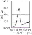
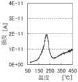
图68A和图68B是示出实施例的TDS分析结果的图;68A and 68B are graphs showing TDS analysis results of an embodiment;
图69A和图69B是示出实施例的TDS分析结果的图;69A and 69B are graphs showing TDS analysis results of an embodiment;
图70A至图70C示出实施例的XRD谱;Figures 70A-70C show XRD spectra of embodiments;
图71A至图71C示出实施例的XRD谱;71A-71C show the XRD spectra of the examples;
图72A至图72C示出实施例的XRD谱;Figures 72A-72C show XRD spectra of embodiments;
图73A至图73E是示出实施例的TDS分析结果的图;73A to 73E are graphs showing TDS analysis results of an embodiment;
图74是实施例的样品的结构的截面示意图;74 is a schematic cross-sectional view of the structure of the sample of the example;
图75A和图75B是示出实施例的CPM测定结果的图;75A and 75B are graphs showing CPM measurement results of the Example;
图76是示出实施例的CPM测定结果的图;76 is a graph showing the CPM measurement results of the Example;
图77A是实施例的晶体管的结构的俯视示意图,图77B和图77C是其截面示意图;77A is a schematic top view of the structure of the transistor of the embodiment, and FIGS. 77B and 77C are schematic cross-sectional views thereof;
图78A至图78C示出实施例的晶体管的Id-Vg特性;78A to 78C illustrate the Id-Vg characteristics of the transistors of the embodiments;
图79A至图79C示出实施例的晶体管的Id-Vg特性;79A to 79C illustrate Id-Vg characteristics of the transistors of the embodiments;
图80A至图80C示出实施例的晶体管的Id-Vg特性;80A-80C illustrate Id-Vg characteristics of the transistors of the embodiments;
图81A至图81C示出实施例的晶体管的Id-Vg特性;81A to 81C illustrate Id-Vg characteristics of the transistors of the embodiments;
图82A至图82C示出实施例的晶体管的Id-Vg特性;82A to 82C illustrate Id-Vg characteristics of the transistors of the embodiments;
图83A至图83C示出实施例的晶体管的Id-Vg特性;83A-83C illustrate Id-Vg characteristics of the transistors of the embodiments;
图84A至图84C示出实施例的晶体管的Id-Vg特性;84A to 84C illustrate the Id-Vg characteristics of the transistors of the embodiments;
图85示出实施例的晶体管的可靠性测试结果;FIG. 85 shows reliability test results of the transistors of the embodiments;
图86示出实施例的晶体管的可靠性测试结果;FIG. 86 shows reliability test results of the transistors of the embodiments;
图87A和图87B示出实施例的有没有光照射的晶体管的Id-Vg特性;87A and 87B show the Id-Vg characteristics of the transistors of the embodiment with and without light irradiation;
图88A和图88B示出实施例的有没有光照射的晶体管的Id-Vg特性;88A and 88B show Id-Vg characteristics of transistors with and without light irradiation of an embodiment;
图89A和图89B示出实施例的有没有光照射的晶体管的Id-Vg特性;89A and 89B show the Id-Vg characteristics of the transistor with and without light irradiation of the embodiment;
图90A和图90B示出实施例的有没有光照射的晶体管的Id-Vg特性。90A and 90B show the Id-Vg characteristics of the transistor with and without light irradiation of the embodiment.
具体实施方式Detailed ways
以下,参照附图说明本发明的实施方式。但是,本发明不局限于以下说明,其方式及详细内容在不脱离本发明的宗旨及其范围的情况下可以被变换为各种各样的形式。因此,本发明不应该被解释为仅局限在实施方式所记载的内容中。Hereinafter, embodiments of the present invention will be described with reference to the accompanying drawings. However, the present invention is not limited to the following description, and the modes and details thereof can be changed into various forms without departing from the spirit and scope of the present invention. Therefore, the present invention should not be construed as being limited only to the contents described in the embodiments.
另外,为了便于理解,有时在附图等中示出的各结构的位置、大小及范围等并不表示其实际的位置、大小及范围等。因此,所公开的发明不一定局限于附图等所公开的位置、大小、范围等。In addition, for ease of understanding, the position, size, range, and the like of each structure shown in the drawings and the like may not represent the actual position, size, range, and the like. Therefore, the disclosed invention is not necessarily limited to the position, size, scope, etc. disclosed in the drawings and the like.
此外,在本说明书等中,为了方便起见,使用“第一”、“第二”等序数词,而其有时并不表示工序顺序或叠层顺序。因此,例如可以将“第一”适当地替换为“第二”或“第三”等来进行说明。此外,本说明书等中的序数词与用于指定本发明的一个方式的序数词有时不一致。In addition, in this specification etc., ordinal numbers, such as "first" and "second", are used for convenience, and may not indicate the order of steps or the order of lamination. Therefore, for example, "first" may be appropriately replaced with "second" or "third" and the like for description. In addition, the ordinal numbers in this specification etc. may not agree with the ordinal numbers for specifying one form of this invention.
在本说明书中,为了方便起见,使用“上”、“下”等表示配置的词句以参照附图说明构成要素的位置关系。另外,构成要素的位置关系根据描述各构成要素的方向适当地改变。因此,不局限于本说明书中所使用的词句,根据情况可以适当地更换。In this specification, for the sake of convenience, words and phrases such as "upper" and "lower" that express arrangement are used to describe the positional relationship of the constituent elements with reference to the drawings. In addition, the positional relationship of the constituent elements is appropriately changed according to the direction in which each constituent element is described. Therefore, it is not limited to the words and phrases used in this specification, and can be appropriately replaced according to the situation.
当在本说明书等中利用附图说明发明的结构时,将共同符号用于不同的附图中的相同部分。When the structure of the invention is described using the drawings in this specification and the like, common symbols are used for the same parts in different drawings.
在本说明书等中,例如当导电性充分低时,有时“半导体”具有“绝缘体”的特性。此外,“半导体”和“绝缘体”的边境不太清楚,因此有时不能精确地区别“半导体”和“绝缘体”。由此,有时可以将本说明书等中的“半导体”称为“绝缘体”。同样地,有时可以将本说明书等中的“绝缘体”称为“半导体”。另外,有时可以将本说明书等中的“绝缘体”称为“半绝缘体”。In this specification and the like, for example, when the electrical conductivity is sufficiently low, a "semiconductor" may have the characteristics of an "insulator". In addition, the border between "semiconductor" and "insulator" is not very clear, so sometimes the precise distinction between "semiconductor" and "insulator" is not possible. Therefore, the "semiconductor" in this specification etc. may be called an "insulator" in some cases. Similarly, the "insulator" in this specification and the like may be referred to as a "semiconductor" in some cases. In addition, the "insulator" in this specification etc. may be called a "semi-insulator".
在本说明书等中,例如当导电性充分高时,有时“半导体”具有“导电体”的特性。此外,“半导体”和“导电体”的边境不太清楚,因此有时不能精确地区别“半导体”和“导电体”。由此,有时可以将本说明书等中的“半导体”称为“导电体”。同样地,有时可以将本说明书等中的“导电体”称为“半导体”。In this specification and the like, for example, when the electrical conductivity is sufficiently high, a "semiconductor" may have the characteristics of a "conductor". In addition, the border between "semiconductor" and "conductor" is not very clear, so sometimes the distinction between "semiconductor" and "conductor" cannot be precisely. Therefore, the "semiconductor" in this specification etc. may be called a "conductor" in some cases. Similarly, the "conductor" in this specification and the like may be referred to as a "semiconductor".
在本说明书等中,晶体管是指至少包括栅极、漏极以及源极这三个端子的元件。此外,晶体管在漏极(漏极端子、漏区域或漏电极)与源极(源极端子、源区域或源电极)之间具有沟道区域,并且电流能够流过漏极、沟道区域以及源极。注意,在本说明书等中,沟道区域是指电流主要流过的区域。In this specification and the like, a transistor refers to an element including at least three terminals of a gate, a drain, and a source. Furthermore, a transistor has a channel region between a drain (drain terminal, drain region or drain electrode) and a source (source terminal, source region or source electrode), and current can flow through the drain, the channel region and source. Note that in this specification and the like, the channel region refers to a region through which current mainly flows.
另外,例如在采用极性不同的晶体管的情况或电路工作中的电流方向变化的情况下,源极和漏极的功能有时互相调换。因此,在本说明书等中,“源极”和“漏极”可以互相调换。In addition, for example, when transistors with different polarities are used, or when the current direction changes during circuit operation, the functions of the source and the drain are sometimes interchanged. Therefore, in this specification and the like, "source" and "drain" may be interchanged with each other.
注意,沟道长度例如是指晶体管的俯视图中的半导体(或在晶体管处于导通状态时,在半导体中电流流过的部分)和栅电极互相重叠的区域或者形成沟道的区域中的源极(源区域或源电极)和漏极(漏区域或漏电极)之间的距离。在一个晶体管中,沟道长度不一定在所有的区域中都成为相同的值。也就是说,一个晶体管的沟道长度有时不限于一个值。因此,在本说明书等中,沟道长度是形成沟道的区域中的任一个值、最大值、最小值或平均值。Note that the channel length refers to, for example, a semiconductor in a plan view of a transistor (or a portion where a current flows in the semiconductor when the transistor is in an on state) and a region where a gate electrode overlaps with each other or a source electrode in a region where a channel is formed The distance between (source region or source electrode) and drain (drain region or drain electrode). In a transistor, the channel length does not necessarily have the same value in all regions. That is, the channel length of one transistor is sometimes not limited to one value. Therefore, in this specification and the like, the channel length is any one value, a maximum value, a minimum value, or an average value in the region where the channel is formed.
沟道宽度例如指半导体(或在晶体管导通时,在半导体中电流流动的部分)与栅电极相互重叠的区域或形成有沟道的区域中的源极与漏极相对的部分的长度。在一个晶体管中,沟道宽度不一定在所有的区域中都成为相同的值。也就是说,一个晶体管的沟道宽度有时不限于一个值。因此,在本说明书等中,沟道宽度是形成沟道的区域中的任一个值、最大值、最小值或平均值。The channel width refers to, for example, the length of a region where a semiconductor (or a portion where a current flows in the semiconductor when a transistor is turned on) and a gate electrode overlap each other, or a portion where the source and drain face each other in the region where the channel is formed. In a transistor, the channel width does not necessarily have the same value in all regions. That is, the channel width of one transistor is sometimes not limited to one value. Therefore, in this specification and the like, the channel width is any one value, a maximum value, a minimum value, or an average value in the region where the channel is formed.
在本说明书等中,“电连接”包括构成要素通过“具有某种电作用的元件”连接的情况。在此,“具有某种电作用的元件”只要可以进行构成要素间的电信号的授受,就对其没有特别的限制。“具有某种电作用的元件”的例子不仅包括电极和布线,而且还包括晶体管等的开关元件、电阻器、电感器、电容器、其他具有各种功能的元件。In the present specification and the like, "electrical connection" includes a case where constituent elements are connected by "an element having a certain electrical effect". Here, the "element having a certain electrical effect" is not particularly limited as long as it can transmit and receive electrical signals between the constituent elements. Examples of the "element having a certain electrical effect" include not only electrodes and wirings, but also switching elements such as transistors, resistors, inductors, capacitors, and other elements having various functions.
电压大多是指某个电位与基准电位(例如,接地电位(GND)或源电位)之间的电位差。由此,可以将电压换称为电位。Voltage mostly refers to the potential difference between a certain potential and a reference potential (eg, ground potential (GND) or source potential). Thus, the voltage can be replaced by the potential.
另外,在本说明书等中,“氧氮化硅膜”是指在其组成中含氧量多于含氮量的膜。氧氮化硅膜优选具有如下范围的氧、氮、硅及氢:55原子%以上且65原子%以下的氧;1原子%以上且20原子%以下的氮;25原子%以上且35原子%以下的硅;0.1原子%以上且10原子%以下的氢。“氮氧化硅膜”是指在其组成中含氮量多于含氧量的膜。氮氧化硅膜优选具有如下浓度范围的氮、氧、硅及氢:55原子%以上且65原子%以下的氮;1原子%以上且20原子%以下的氧;25原子%以上且35原子%以下的硅;0.1原子%以上且10原子%以下的氢。In addition, in this specification etc., a "silicon oxynitride film" means a film which contains more oxygen content than nitrogen content in the composition. The silicon oxynitride film preferably has oxygen, nitrogen, silicon, and hydrogen in the following ranges: oxygen of 55 atomic % or more and 65 atomic % or less; nitrogen of 1 atomic % or more and 20 atomic % or less; 25 atomic % or more and 35 atomic % The following silicon; 0.1 atomic % or more and 10 atomic % or less hydrogen. "Silicon oxynitride film" refers to a film containing more nitrogen than oxygen in its composition. The silicon oxynitride film preferably has nitrogen, oxygen, silicon and hydrogen in the following concentration ranges: nitrogen at 55 atomic % or more and 65 at % or less; oxygen at 1 at % or more and 20 at % or less; 25 at % or more and 35 at % The following silicon; 0.1 atomic % or more and 10 atomic % or less hydrogen.
在本说明书等中,可以将“膜”和“层”相互调换。例如,有时可以将“导电层”更换为“导电膜”。此外,有时可以将“绝缘膜”更换为“绝缘层”。In this specification and the like, "film" and "layer" may be interchanged with each other. For example, "conductive layer" may sometimes be replaced with "conductive film". In addition, "insulating film" may be replaced with "insulating layer" in some cases.
在本说明书中,“平行”是指两条直线形成的角度为-10°以上且10°以下的状态,因此,也包括该角度为-5°以上且5°以下的状态。“大致平行”是指两条直线形成的角度为-30°以上且30°以下的状态。另外,“垂直”是指两条直线形成的角度为80°以上且100°以下的状态,因此也包括85°以上且95°以下的角度的状态。“大致垂直”是指两条直线形成的角度为60°以上且120°以下的状态。In this specification, "parallel" refers to a state where the angle formed by two straight lines is -10° or more and 10° or less, and therefore includes a state where the angle is -5° or more and 5° or less. "Substantially parallel" refers to a state where the angle formed by the two straight lines is -30° or more and 30° or less. In addition, "perpendicular" means a state in which the angle formed by two straight lines is 80° or more and 100° or less, and therefore also includes a state in which an angle of 85° or more and 95° or less is included. "Substantially perpendicular" refers to a state where the angle formed by two straight lines is 60° or more and 120° or less.
注意,半导体的杂质是指半导体的主要成分之外的元素。例如,浓度低于0.1atomic%的元素是杂质。当包含杂质时,有可能在半导体中形成DOS(density ofstates:态密度),载流子迁移率有可能降低或结晶性有可能降低。在半导体包含氧化物半导体时,作为改变半导体特性的杂质的例子,有第1族元素、第2族元素、第14族元素、第15族元素以及主要成分之外的过渡金属,尤其是,例如有氢(包含于水中)、锂、钠、硅、硼、磷、碳、氮。当半导体是氧化物半导体时,有时由于氢等杂质的混入导致氧缺陷的产生。此外,当半导体包含硅时,作为改变半导体特性的杂质,例如有氧、除氢之外的第1族元素、第2族元素、第13族元素、第15族元素。Note that the impurities of the semiconductor refer to elements other than the main components of the semiconductor. For example, an element whose concentration is lower than 0.1 atomic % is an impurity. When an impurity is included, DOS (density of states: density of states) may be formed in the semiconductor, and carrier mobility or crystallinity may be lowered. When the semiconductor includes an oxide semiconductor, examples of impurities that change the characteristics of the semiconductor include a
实施方式1
在本实施方式中,对本发明的一个方式的氧化物半导体膜进行说明。In this embodiment mode, an oxide semiconductor film according to one embodiment of the present invention will be described.
<1-1.氧化物半导体膜><1-1. Oxide semiconductor film>
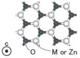
本发明的一个方式的氧化物半导体膜包括铟(In)、M(M是Al、Ga、Y或Sn)及锌(Zn)。The oxide semiconductor film of one embodiment of the present invention includes indium (In), M (M is Al, Ga, Y, or Sn), and zinc (Zn).
包含In的氧化物半导体膜例如具有高载流子迁移率(电子迁移率)。氧化物半导体膜通过包含元素M例如具有高能隙(Eg)。该元素M是与氧的键能高的元素,元素M与氧的键能比In与氧的键能高。当氧化物半导体膜包含Zn时,氧化物半导体膜容易晶化。The oxide semiconductor film containing In has, for example, high carrier mobility (electron mobility). The oxide semiconductor film has, for example, a high energy gap (Eg) by containing the element M. The element M is an element having a high bond energy with oxygen, and the bond energy between the element M and oxygen is higher than the bond energy between In and oxygen. When the oxide semiconductor film contains Zn, the oxide semiconductor film is easily crystallized.
典型的是,作为本发明的一个方式的氧化物半导体膜,可以使用In-Ga氧化物、In-Zn氧化物或In-M-Zn氧化物。尤其是,作为氧化物半导体膜,优选使用以M为Ga的In-M-Zn氧化物(即In-Ga-Zn氧化物;以下,有时称为IGZO)。Typically, In-Ga oxide, In-Zn oxide, or In-M-Zn oxide can be used as the oxide semiconductor film of one embodiment of the present invention. In particular, it is preferable to use an In-M-Zn oxide in which M is Ga (ie, In-Ga-Zn oxide; hereinafter, sometimes referred to as IGZO) as the oxide semiconductor film.
当氧化物半导体膜为In-M-Zn氧化物时,用来形成In-M-Zn氧化物的溅射靶材的金属元素的原子个数比优选满足In≥M、Zn≥M。作为这种溅射靶材的金属元素的原子个数比,优选为In:M:Zn=1:1:1、In:M:Zn=1:1:1.2、In:M:Zn=2:1:3、In:M:Zn=3:1:2、In:M:Zn=4:2:4.1。注意,氧化物半导体膜中的金属元素的原子个数比在上述溅射靶材中的金属元素的原子个数比的±40%的范围内变动作为误差。例如,在使用In、Ga和Zn的原子个数比为4:2:4.1的溅射靶材时,有时氧化物半导体膜中的In、Ga和Zn的原子个数比为4:2:3或4:2:3附近。When the oxide semiconductor film is an In-M-Zn oxide, the atomic ratio of the metal element of the sputtering target for forming the In-M-Zn oxide preferably satisfies In≧M and Zn≧M. As the atomic ratio of metal elements in such a sputtering target, In:M:Zn=1:1:1, In:M:Zn=1:1:1.2, In:M:Zn=2: 1:3, In:M:Zn=3:1:2, In:M:Zn=4:2:4.1. Note that the atomic number ratio of the metal element in the oxide semiconductor film varies within a range of ±40% of the atomic number ratio of the metal element in the above-described sputtering target as an error. For example, when a sputtering target having an atomic ratio of In, Ga, and Zn of 4:2:4.1 is used, the atomic ratio of In, Ga, and Zn in the oxide semiconductor film may be 4:2:3. or around 4:2:3.
氧化物半导体膜的能隙为2eV以上,优选为2.5eV以上,更优选为3eV以上。The energy gap of the oxide semiconductor film is 2 eV or more, preferably 2.5 eV or more, and more preferably 3 eV or more.
当制造在其沟道区域包括氧化物半导体膜的晶体管时,混入沟道区域的氧化物半导体膜中的氢或水分等杂质对晶体管特性造成影响,所以会成为问题。因此,在氧化物半导体膜的沟道区域中,氢或水分等杂质越少越好。When a transistor including an oxide semiconductor film in its channel region is manufactured, impurities such as hydrogen and moisture mixed into the oxide semiconductor film in the channel region affect transistor characteristics, which poses a problem. Therefore, in the channel region of the oxide semiconductor film, the less impurities such as hydrogen and moisture, the better.
另外,形成在沟道区域的氧化物半导体膜中的氧缺陷对晶体管特性造成影响,所以会成为问题。例如,形成在沟道区域的氧化物半导体膜中的氧缺陷与氢键合而成为载流子供应源。在沟道区域的氧化物半导体膜中产生的载流子供应源会引起具有氧化物半导体膜的晶体管的电特性的变动,典型地发生阈值电压的漂移。此外,有各晶体管的电特性不均匀的问题。因此,在氧化物半导体膜的沟道区域中,氧缺陷越少越好。In addition, oxygen vacancies formed in the oxide semiconductor film in the channel region have an influence on transistor characteristics, and thus become a problem. For example, oxygen vacancies formed in the oxide semiconductor film in the channel region are bonded with hydrogen to become a carrier supply source. A carrier supply source generated in the oxide semiconductor film in the channel region causes fluctuations in electrical characteristics of transistors including the oxide semiconductor film, and typically shifts in threshold voltage. In addition, there is a problem that the electrical characteristics of each transistor are not uniform. Therefore, in the channel region of the oxide semiconductor film, the fewer oxygen vacancies, the better.
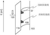
当在氧化物半导体膜的内部、以及氧化物半导体膜与外部的界面存在有缺陷能级时,该缺陷能级会引起包括氧化物半导体膜的晶体管的劣化等。因此,为了获得包括氧化物半导体膜的晶体管的稳定电特性,重要的是减少氧化物半导体膜的内部及其界面附近的缺陷能级或缺陷态密度。When a defect level exists inside the oxide semiconductor film and at the interface between the oxide semiconductor film and the outside, the defect level causes deterioration of a transistor including the oxide semiconductor film, or the like. Therefore, in order to obtain stable electrical characteristics of a transistor including an oxide semiconductor film, it is important to reduce the defect level or defect state density inside the oxide semiconductor film and in the vicinity of the interface.
缺陷能级含有浅位置的缺陷能级和深位置的缺陷能级。注意,在本说明书等中,浅位置的缺陷能级是指导带底的能量(Ec)与带隙中心(mid gap)之间的缺陷能级。因此,例如,浅位置的缺陷能级位于导带底的能量附近。在本说明书等中,深位置的缺陷能级是指价带顶的能量(Ev)与带隙中心之间的缺陷能级。由此,例如,深位置的缺陷能级与价带顶的能量之间相比更靠近于带隙中心。The defect level contains the defect level at the shallow position and the defect level at the deep position. Note that, in this specification and the like, the defect level at the shallow position is the defect level between the energy (Ec) of the guidance band bottom and the center of the band gap (mid gap). Thus, for example, the defect level at the shallow position is located near the energy of the bottom of the conduction band. In the present specification and the like, the defect level at the deep position refers to the defect level between the energy (Ev) of the top of the valence band and the center of the band gap. Thus, for example, the defect level at the deep position is closer to the center of the band gap than the energy at the top of the valence band.
通过在氧化物半导体膜的内部、以及氧化物半导体膜与外部的界面减少浅缺陷能级或浅缺陷态密度,可以提高包括氧化物半导体膜的晶体管的场效应迁移率(简单地称为迁移率或μFE)。此外,可以减小包括氧化物半导体膜的晶体管的电特性变动。By reducing the shallow defect level or the shallow defect state density inside the oxide semiconductor film and at the interface between the oxide semiconductor film and the outside, the field effect mobility (simply referred to as mobility) of the transistor including the oxide semiconductor film can be improved or μFE). Furthermore, variation in electrical characteristics of the transistor including the oxide semiconductor film can be reduced.
于是,在本发明的一个方式中,减少氧化物半导体膜中的杂质(典型为氢或水分)、氧缺陷和/或缺陷态密度。为了减少氧化物半导体膜中的杂质、氧缺陷或缺陷态密度,优选提高该氧化物半导体膜的结晶性。Thus, in one embodiment of the present invention, impurities (typically, hydrogen or moisture), oxygen defects, and/or defect state density in the oxide semiconductor film are reduced. In order to reduce impurities, oxygen defects, or density of defect states in the oxide semiconductor film, it is preferable to increase the crystallinity of the oxide semiconductor film.
<1-2.氧化物半导体的结构><1-2. Structure of oxide semiconductor>
在此,对本发明的一个方式的氧化物半导体膜所包含的氧化物半导体的结构进行说明。Here, the structure of the oxide semiconductor included in the oxide semiconductor film of one embodiment of the present invention will be described.
氧化物半导体被分为单晶氧化物半导体和非单晶氧化物半导体。作为非单晶氧化物半导体的例子,有CAAC-OS(c-axis aligned crystalline oxide semiconductor:c轴取向结晶氧化物半导体)、多晶氧化物半导体、nc-OS(nanocrystalline oxidesemiconductor:纳米晶氧化物半导体)、a-like OS(amorphous like oxidesemiconductor)以及非晶氧化物半导体。Oxide semiconductors are classified into single crystal oxide semiconductors and non-single crystal oxide semiconductors. Examples of non-single crystal oxide semiconductors include CAAC-OS (c-axis aligned crystalline oxide semiconductor: c-axis aligned crystalline oxide semiconductor), polycrystalline oxide semiconductor, nc-OS (nanocrystalline oxidesemiconductor: nanocrystalline oxide semiconductor) ), a-like OS (amorphous like oxidesemiconductor) and amorphous oxide semiconductors.
从其他观点看来,氧化物半导体被分为非晶氧化物半导体和结晶氧化物半导体。作为结晶氧化物半导体的例子,有单晶氧化物半导体、CAAC-OS、多晶氧化物半导体以及nc-OS。From other viewpoints, oxide semiconductors are classified into amorphous oxide semiconductors and crystalline oxide semiconductors. As examples of crystalline oxide semiconductors, there are single crystal oxide semiconductors, CAAC-OS, polycrystalline oxide semiconductors, and nc-OS.
已知:非晶结构一般被定义为处于亚稳态并没有被固定化,具有各向同性而不具有不均匀结构。换言之,非晶结构的键角不固定,具有短程有序,而不具有长程有序。Known: Amorphous structure is generally defined as being in a metastable state and not being immobilized, being isotropic and not having an inhomogeneous structure. In other words, the bond angles of the amorphous structure are not fixed and have short-range order but not long-range order.
这意味着,不能将实质上稳定的氧化物半导体称为完全非晶(completelyamorphous)氧化物半导体。另外,不能将不具有各向同性的氧化物半导体(例如,在微小区域中具有周期结构的氧化物半导体)称为完全非晶氧化物半导体。注意,a-like OS在微小区域中具有周期结构,但是同时具有空洞(void),并具有不稳定的结构。因此,a-like OS在物性上近乎于非晶氧化物半导体。This means that a substantially stable oxide semiconductor cannot be called a completely amorphous oxide semiconductor. In addition, an oxide semiconductor that does not have isotropy (for example, an oxide semiconductor having a periodic structure in a minute region) cannot be called a completely amorphous oxide semiconductor. Note that the a-like OS has a periodic structure in a tiny region, but at the same time has a void, and has an unstable structure. Therefore, a-like OS is close to amorphous oxide semiconductor in physical properties.
作为本发明的一个方式的氧化物半导体膜,在上述氧化物半导体中尤其优选的是CAAC-OS。当氧化物半导体膜为CAAC-OS时,能够提高氧化物半导体膜的结晶性并减少氧化物半导体膜中的杂质、氧缺陷或缺陷态密度。关于上述CAAC-OS、nc-OS、a-like OS等,将在后面详细地说明。Among the oxide semiconductors described above, CAAC-OS is particularly preferable as the oxide semiconductor film of one embodiment of the present invention. When the oxide semiconductor film is CAAC-OS, the crystallinity of the oxide semiconductor film can be improved and impurities, oxygen defects or defect state density in the oxide semiconductor film can be reduced. The above-mentioned CAAC-OS, nc-OS, a-like OS, etc. will be described in detail later.
在此,参照图1A和图1B、图2A和图2B、图3A和图3B、图4、图5A和图5B对本发明的一个方式的氧化物半导体膜的结晶性进行说明。Here, the crystallinity of the oxide semiconductor film according to one embodiment of the present invention will be described with reference to FIGS. 1A and 1B, FIGS. 2A and 2B, FIGS. 3A and 3B, FIGS.
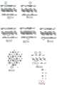
<1-3.氧化物半导体膜的结晶性><1-3. Crystallinity of oxide semiconductor film>
通过使用透射电子显微镜(TEM:transmission electron microscope)分析氧化物半导体膜的截面并使用X射线衍射(XRD:X-ray diffraction)分析该氧化物半导体膜,可以对氧化物半导体膜的结晶性进行评价。形成TEM分析用氧化物半导体膜和XRD分析用氧化物半导体膜,并对其结晶性进行评价。The crystallinity of the oxide semiconductor film can be evaluated by analyzing the cross section of the oxide semiconductor film using a transmission electron microscope (TEM: transmission electron microscope) and analyzing the oxide semiconductor film using X-ray diffraction (XRD: X-ray diffraction). . An oxide semiconductor film for TEM analysis and an oxide semiconductor film for XRD analysis were formed, and their crystallinity was evaluated.
《TEM分析用氧化物半导体膜的形成方法》"Method for forming an oxide semiconductor film for TEM analysis"
首先,对TEM分析用氧化物半导体膜的形成方法进行说明。在720mm×600mm的玻璃衬底上形成厚度为35nm的TEM分析用氧化物半导体膜。通过溅射法形成该氧化物半导体膜。另外,该氧化物半导体膜的成膜条件为如下:衬底温度为170℃;将流量为100sccm的氩气体及流量为100sccm的氧气体引入到处理室内;压力为0.6Pa;对多晶金属氧化物溅射靶材(具有In:Ga:Zn=1:1:1.2的原子数比)供应2500W的AC功率。First, a method for forming an oxide semiconductor film for TEM analysis will be described. An oxide semiconductor film for TEM analysis was formed with a thickness of 35 nm on a glass substrate of 720 mm×600 mm. The oxide semiconductor film is formed by sputtering. In addition, the film formation conditions of the oxide semiconductor film were as follows: the substrate temperature was 170° C.; the argon gas with a flow rate of 100 sccm and the oxygen gas with a flow rate of 100 sccm were introduced into the processing chamber; the pressure was 0.6 Pa; the polycrystalline metal was oxidized A sputtering target (with an atomic ratio of In:Ga:Zn=1:1:1.2) was supplied with 2500W of AC power.
接着,进行上述氧化物半导体膜的TEM分析。Next, TEM analysis of the above-mentioned oxide semiconductor film was performed.
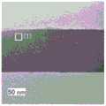
图4示出进行TEM分析时的720mm×600mm的玻璃衬底的坐标。在图4中,将衬底的720mm长的一边分为6个,由此,衬底包括区域1至6。另外,将衬底的600mm长的一边分为15个,由此,衬底包括区域A至O。以下,将衬底上的各区域例如称为如下:将衬底中央附近称为区域H3,该区域H3在衬底的一边为600mm的方向上离衬底中央的距离在-20mm至20mm的范围内,并且在衬底的一边为720mm的方向上离衬底中央的距离在0mm至120mm的范围内。对图4所示的区域B3及区域H3进行TEM分析。另外,有时将区域B3及H3分别称为衬底外周及衬底中央。FIG. 4 shows the coordinates of a 720 mm×600 mm glass substrate when TEM analysis was performed. In FIG. 4 , the 720 mm long side of the substrate is divided into six, whereby the substrate includes
《TEM分析》"TEM Analysis"
使用日本电子株式会社制造的原子分辨率分析电子显微镜JEM-ARM200F进行TEM分析。在该测量中,加速电压为200kV,倍率为400万倍。TEM analysis was performed using an atomic resolution analysis electron microscope JEM-ARM200F manufactured by JEOL Ltd. In this measurement, the acceleration voltage was 200 kV and the magnification was 4 million times.
图1A和图1B示出氧化物半导体膜的截面TEM图像。图1A是衬底中央(区域H3)的截面TEM图像,图1B是衬底外周(区域B3)的截面TEM图像。1A and 1B show cross-sectional TEM images of the oxide semiconductor film. FIG. 1A is a cross-sectional TEM image of the center of the substrate (region H3 ), and FIG. 1B is a cross-sectional TEM image of the outer periphery of the substrate (region B3 ).
如图1A和图1B所示,本发明的一个方式的氧化物半导体膜在进行截面TEM分析时能够确认到原子的截面TEM图像的一个视野中包括具有c轴取向性的区域(以下,也称为第一区域)。As shown in FIGS. 1A and 1B , in the oxide semiconductor film according to one embodiment of the present invention, when a cross-sectional TEM analysis is performed, it can be confirmed that a region having a c-axis orientation (hereinafter, also referred to as a region having c-axis orientation) is included in one field of view of a cross-sectional TEM image of atoms. for the first region).
由于在图1A和图1B中有时不能明确地确认到具有c轴取向性的区域(第一区域),所以图2A和图2B示出在图1A和图1B的截面TEM图像中划辅助线的TEM图像。图2A是在图1A中划作为辅助线的白色线的截面TEM图像,图2B是在图1B中划作为辅助线的白色线的截面TEM图像。在图2A和图2B中,白色辅助线沿着具有c轴取向性的区域(第一区域)的格子条纹。Since the region (first region) having the c-axis orientation may not be clearly recognized in FIGS. 1A and 1B , FIGS. 2A and 2B show an auxiliary line drawn in the cross-sectional TEM images of FIGS. 1A and 1B . TEM image. 2A is a cross-sectional TEM image of a white line drawn as an auxiliary line in FIG. 1A , and FIG. 2B is a cross-sectional TEM image of a white line drawn as an auxiliary line in FIG. 1B . In FIGS. 2A and 2B , the white auxiliary lines are along the lattice stripes of the region (first region) having the c-axis orientation.
如图2A和图2B所示,当进行截面TEM分析时,本发明的一个方式的氧化物半导体膜在能够确认到原子的截面TEM图像的一个视野中包括具有c轴取向性的区域(第一区域)和不具有c轴取向性的区域(以下,也称为第二区域)。第一区域可以被换称为c轴取向于与膜的顶面的法线向量平行的方向的区域。第二区域可以被换称为不具有取向性的区域或者不容易观察到c轴取向性的区域。注意,有时将第二区域称为原子空隙(atomic void)。As shown in FIGS. 2A and 2B , when a cross-sectional TEM analysis is performed, the oxide semiconductor film of one embodiment of the present invention includes a region having c-axis orientation in one field of view in which a cross-sectional TEM image of atoms can be confirmed (first region) and a region without c-axis orientation (hereinafter, also referred to as a second region). The first region can be interchangeably referred to as a region in which the c-axis is oriented in a direction parallel to the normal vector of the top surface of the film. The second region may be referred to as a region having no orientation or a region where the c-axis orientation is not easily observed. Note that the second region is sometimes referred to as an atomic void.
根据图2A所示的衬底中央(区域H3)的氧化物半导体膜与图2B所示的衬底外周(区域B3)的氧化物半导体膜之间的比较可知:图2A所示的衬底中央(区域H3)的氧化物半导体膜中的具有c轴取向性的区域(第一区域)所占的比率更多。From the comparison between the oxide semiconductor film in the center of the substrate (region H3 ) shown in FIG. 2A and the oxide semiconductor film in the periphery of the substrate (region B3 ) shown in FIG. 2B , it can be seen that the center of the substrate shown in FIG. 2A The ratio of the region (first region) having c-axis orientation in the oxide semiconductor film of (region H3 ) is larger.
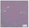
在此,为了算出图2A和图2B的氧化物半导体膜中的具有c轴取向性的区域(第一区域)和不具有c轴取向性的区域(第二区域)的面积,进行图像分析,并算出这些区域的比率。Here, in order to calculate the area of a region (first region) having c-axis orientation and a region (second region) not having c-axis orientation in the oxide semiconductor film of FIGS. 2A and 2B , image analysis was performed, and calculate the ratio of these areas.
图3A和图3B示出图2A和图2B的氧化物半导体膜的截面TEM图像的图像分析结果。图3A示出图2A的图像分析结果,图3B示出图2B的图像分析结果。在此,对图3A和图3B所示的区域10的部分(在此,截面TEM图像的一个面积为30nm2左右的部分)进行定量化。注意,进行定量化的区域10的部分不局限于上述部分,例如可以是截面TEM图像的面积为5nm2以上且500nm2以下的部分,优选为5nm2以上且100nm2以下的部分,更优选为5nm2以上且50nm2以下的部分。3A and 3B illustrate image analysis results of cross-sectional TEM images of the oxide semiconductor film of FIGS. 2A and 2B . FIG. 3A shows the image analysis result of FIG. 2A , and FIG. 3B shows the image analysis result of FIG. 2B . Here, the portion of the
在图3A和图3B中,白色的区域11是具有c轴取向性的区域(第一区域),灰色的区域12是不具有c轴取向性的区域(第二区域)。In FIGS. 3A and 3B , the
由图3A和图3B的截面TEM图像的图像分析结果可知,图3A的第一区域的面积为76.7%,第二区域的面积为23.3%。图3B的第一区域的面积为52.8%,第二区域的面积为47.2%。From the image analysis results of the cross-sectional TEM images of FIGS. 3A and 3B , it can be seen that the area of the first region in FIG. 3A is 76.7%, and the area of the second region is 23.3%. The area of the first region of FIG. 3B is 52.8%, and the area of the second region is 47.2%.
当与具有c轴取向性的区域(第一区域)不同的区域(换言之,不具有c轴取向性的区域(第二区域))的面积小于50%,优选小于30%,更优选小于10%且包括0%时,本发明的一个方式的氧化物半导体膜可以具有高结晶性。When the area of a region different from the region having c-axis orientation (first region) (in other words, region not having c-axis orientation (second region)) is less than 50%, preferably less than 30%, more preferably less than 10% In addition, when 0% is included, the oxide semiconductor film of one embodiment of the present invention can have high crystallinity.
《XRD分析用氧化物半导体膜的形成方法》"Method for forming an oxide semiconductor film for XRD analysis"
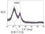
接着,对XRD分析用氧化物半导体膜的制造方法进行说明。在720mm×600mm的玻璃衬底上形成厚度为100nm的XRD分析用氧化物半导体膜。通过溅射法形成该氧化物半导体膜。另外,该氧化物半导体膜的成膜条件为如下:衬底温度为170℃;将流量为100sccm的氩气体及流量为100sccm的氧气体引入到处理室内;压力为0.6Pa;对多晶金属氧化物溅射靶材(具有In:Ga:Zn=1:1:1.2的原子数比)供应2500W的AC功率。Next, the manufacturing method of the oxide semiconductor film for XRD analysis is demonstrated. An oxide semiconductor film for XRD analysis with a thickness of 100 nm was formed on a glass substrate of 720 mm×600 mm. The oxide semiconductor film is formed by sputtering. In addition, the film formation conditions of the oxide semiconductor film were as follows: the substrate temperature was 170° C.; the argon gas with a flow rate of 100 sccm and the oxygen gas with a flow rate of 100 sccm were introduced into the processing chamber; the pressure was 0.6 Pa; the polycrystalline metal was oxidized A sputtering target (with an atomic ratio of In:Ga:Zn=1:1:1.2) was supplied with 2500W of AC power.
接着,对上述氧化物半导体膜进行XRD分析。Next, XRD analysis was performed on the above-mentioned oxide semiconductor film.
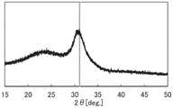
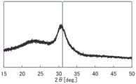
进行XRD分析的720mm×600mm的玻璃衬底的坐标与如上所述的TEM分析相同。换言之,对图4所示的衬底中央(区域H3)及衬底外周(区域B3)进行XRD分析。The coordinates of the 720 mm x 600 mm glass substrate for the XRD analysis were the same as for the TEM analysis as described above. In other words, XRD analysis was performed on the substrate center (region H3 ) and the substrate outer periphery (region B3 ) shown in FIG. 4 .
《XRD分析》"XRD Analysis"
通过使用具有多功能的用来评价薄膜材料的X射线衍射仪D8DISCOVER Hybrid(美国布鲁克AXS公司制造)进行XRD分析。在XRD分析中采用out-of-plane法。The XRD analysis was performed by using an X-ray diffractometer D8DISCOVER Hybrid (manufactured by Bruker AXS, USA) having a multifunctionality for evaluating thin film materials. The out-of-plane method was used in the XRD analysis.
图5A和图5B示出氧化物半导体膜的XRD分析结果。图5A示出衬底中央(区域H3)的XRD结果,图5B示出衬底外周(区域B3)的XRD结果。5A and 5B show the results of XRD analysis of the oxide semiconductor film. FIG. 5A shows the XRD result of the center of the substrate (region H3 ), and FIG. 5B shows the XRD result of the outer periphery of the substrate (region B3 ).
如图5A和图5B所示,衬底中央(区域H3)的氧化物半导体膜和衬底外周(区域B3)的氧化物半导体膜都在2θ=31°附近呈现峰值。2θ=31°附近的峰值来源于InGaZnO4结晶的(009)面,由此可知,在衬底中央及外周处氧化物半导体膜中的结晶具有c轴取向性,并且该c轴朝向大致垂直于形成面或顶面的方向。此外,图5A和图5B所示的2θ=24°附近的峰值来源于玻璃衬底。As shown in FIGS. 5A and 5B , both the oxide semiconductor film in the center of the substrate (region H3 ) and the oxide semiconductor film in the periphery of the substrate (region B3 ) exhibit peaks around 2θ=31°. The peak near 2θ=31° originates from the (009) plane of the InGaZnO4 crystal. From this, it can be seen that the crystal in the oxide semiconductor film has a c-axis orientation at the center and periphery of the substrate, and the c-axis is oriented approximately perpendicular to Orientation to form the face or top face. In addition, the peak in the vicinity of 2θ=24° shown in FIGS. 5A and 5B is derived from the glass substrate.
图5B所示的衬底外周(区域B3)的氧化物半导体膜在2θ=36°附近呈现峰值。2θ=36°附近的峰值来源于尖晶石型结晶结构。由此可以认为:衬底外周(区域B3)的氧化物半导体膜包含具有c轴取向性的结晶之外的结晶。The oxide semiconductor film on the periphery of the substrate (region B3 ) shown in FIG. 5B exhibits a peak around 2θ=36°. The peak near 2θ=36° is derived from the spinel-type crystal structure. From this, it is considered that the oxide semiconductor film on the periphery of the substrate (region B3 ) contains crystals other than crystals having c-axis orientation.
<1-4.缺陷态密度的评价方法><1-4. Evaluation method of defect state density>
接着,参照图6、图7A和图7B、图8A至图8C以及图9对氧化物半导体膜中的缺陷态密度的评价方法进行说明。例如,通过比较晶体管的高频C-V特性的测量值与C-V特性的计算值,可以对缺陷态密度进行评价。Next, a method for evaluating the density of defect states in the oxide semiconductor film will be described with reference to FIGS. 6 , 7A and 7B , 8A to 8C , and 9 . For example, the density of defect states can be evaluated by comparing the measured value of the high frequency C-V characteristic of the transistor with the calculated value of the C-V characteristic.
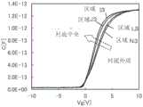
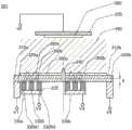
图6是用于计算的晶体管的截面示意图。图6所示的晶体管包括绝缘膜103、氧化物半导体膜108、导电膜112a、112b、绝缘膜116以及导电膜120。氧化物半导体膜108包括隔着绝缘膜116重叠于导电膜120的区域。导电膜120被用作栅电极。绝缘膜116被用作栅极绝缘膜。导电膜112a、112b接触于氧化物半导体膜108并被用作源电极及漏电极。实际上制造并用于测量的晶体管也具有同样的截面结构。FIG. 6 is a schematic cross-sectional view of a transistor used for calculation. The transistor shown in FIG. 6 includes an insulating
使用Silvaco公司制造的器件仿真器“ATLAS”进行C-V特性的计算。表1示出用于计算的参数。此外,Eg表示能隙,Nc表示导带的实效状态密度,Nv表示价带的实效状态密度。The calculation of the C-V characteristics was performed using a device simulator "ATLAS" manufactured by Silvaco Corporation. Table 1 shows the parameters used for the calculation. In addition, Eg represents the energy gap, Nc represents the effective state density of the conduction band, and Nv represents the effective state density of the valence band.
[表1][Table 1]

导电膜112a、112b与氧化物半导体膜108接触的区域中的氧化物半导体膜108的供体密度为1×1019cm-3。The donor density of the
图7A示出通过计算得到的理想的C-V特性及对所制造的晶体管进行测量的C-V特性。在实际上制造并测量的晶体管中,作为氧化物半导体膜108使用具有表1所示的物性的In-Ga-Zn氧化物。以如下方式进行C-V特性的测量:在导电膜112a及112b与导电膜120之间以0.1V间隔施加-10V至10V的电压(栅极电压Vg),接着以0.1V间隔施加10V至-10V的电压。作为栅极电压Vg,施加1kHz的交流电压及直流电压。FIG. 7A shows ideal C-V characteristics obtained by calculation and C-V characteristics measured on the fabricated transistor. In a transistor actually manufactured and measured, In-Ga-Zn oxide having the physical properties shown in Table 1 was used as the
在晶体管的沟道长度很大而不能充分反映测量区域中的电容的变化的情况下,有时交流电压频率的提高导致电容的测量值的降低。例如,在晶体管的沟道长度小于1000μm的情况下,即使使用高于1kHz的频率的交流电压也可以充分反应测量区域中的电容的变化。因此,根据晶体管的沟道长度可以适当地选择交流电压的频率。在实际上的晶体管的沟道长度上交流电压的频率例如为0.1kHz以上且10MHz以下、0.2kHz以上且1MHz以下、0.3kHz以上且100kHz以下或者0.3kHz以上且10kHz以下。In the case where the channel length of the transistor is too large to sufficiently reflect the change in capacitance in the measurement region, an increase in the frequency of the AC voltage sometimes results in a decrease in the measured value of the capacitance. For example, in the case where the channel length of the transistor is less than 1000 μm, the change in capacitance in the measurement region can be sufficiently reflected even if an AC voltage with a frequency higher than 1 kHz is used. Therefore, the frequency of the AC voltage can be appropriately selected according to the channel length of the transistor. The frequency of the AC voltage over the actual channel length of the transistor is, for example, 0.1 kHz or more and 10 MHz or less, 0.2 kHz or more and 1 MHz or less, 0.3 kHz or more and 100 kHz or less, or 0.3 kHz or more and 10 kHz or less.
如图7A所示,与通过计算得到的理想的C-V特性相比,实际测量的C-V特性的相对于栅极电压Vg的电容的变化缓慢。这是因为位于导带底的能量附近的浅缺陷能级俘获电子。As shown in FIG. 7A , the change in capacitance with respect to the gate voltage Vg of the actually measured C-V characteristics is slow compared to the ideal C-V characteristics obtained by calculation. This is because electrons are trapped by shallow defect levels located near the energy of the bottom of the conduction band.
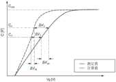
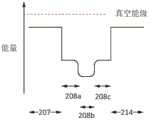
例如,在图8A所示的能带结构中,当栅极电压Vg为开始积累的栅极电压Vg(表示为V0)时,在氧化物半导体膜108的能隙内的浅缺陷能级中电子不被俘获,而在深缺陷能级中电子被俘获。另一方面,在作为栅极电压Vg施加正电压的图8B所示的能带结构中,氧化物半导体膜108的能带弯曲,由此在浅缺陷能级中电子也被俘获。这是根据浅缺陷能级或深缺陷能级与费米能级Ef的关系而可以理解。For example, in the energy band structure shown in FIG. 8A , when the gate voltage Vg is the gate voltage Vg (denoted as V0 ) at which accumulation starts, electrons in the shallow defect level within the energy gap of the
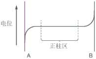
当栅极电压Vg小于V0时,在浅缺陷能级中不发生电子的俘获及解俘获,由此在计算值与实测值之间不产生差异。另外,即使栅极电压Vg高于导带底的能量与费米能级一致的栅极电压Vg(表示为V1),在氧化物半导体膜108与绝缘膜116的界面也不会发生浅缺陷能级中的电子的俘获及解俘获,因此在计算值与实测值之间不产生差异。因此,如图8C所示,在栅极电压Vg为V0至V1的范围内时可以对浅缺陷能级进行评价。When the gate voltage Vg is less than V0, trapping and de-trapping of electrons do not occur in the shallow defect level, and thus no difference occurs between the calculated value and the measured value. In addition, even if the gate voltage Vg is higher than the gate voltage Vg (represented as V1) at which the energy at the bottom of the conduction band coincides with the Fermi level, shallow defect energy does not occur at the interface between the
例如,使用图9所示的示意性的C-V特性对浅缺陷态密度的评价方法进行说明。在通过计算得到的理想的C-V特性上,将电容从C1变化到C2时的栅极电压Vg的变化表示为ΔVid。在实测的C-V特性上,将电容从C1变化到C2时的栅极电压Vg的变化称为ΔVex。将电容从C1变化到C2时的氧化物半导体膜108与绝缘膜116的界面的电位的变化量称为
在图9中,实际测量值的C-V特性的倾斜度与计算值相比逐渐变化,由此可知ΔVid一直小于ΔVex。此时,ΔVex与ΔVid之间的差异对应于在浅缺陷能级中俘获电子时需要的电位差。因此,当将在氧化物半导体膜108与绝缘膜116的界面被俘获的电子所引起的电荷的变化量表示为ΔQSS,并且将绝缘膜116的电容表示为COX时,ΔQSS可以以下面的算式1表示。In FIG. 9 , the inclination of the CV characteristic of the actual measured value gradually changes from the calculated value, and it can be seen that ΔVid is always smaller than ΔVex . At this time, the difference between ΔVex and ΔVid corresponds to the potential difference required to trap electrons in the shallow defect level. Therefore, when the amount of change in charge caused by electrons trapped at the interface of the
[算式1][Equation 1]
ΔQSS=COX(ΔVex-ΔVid) (1)ΔQSS =COX (ΔVex -ΔVid ) (1)
另外,在NSS为将界面的每个单位面积乘以能量的浅缺陷态密度,A为晶体管的沟道区的面积时,ΔQSS可以以算式2表示。此外,q表示元电荷。In addition, when NSS is the shallow defect state density obtained by multiplying the energy per unit area of the interface, and A is the area of the channel region of the transistor, ΔQSS can be expressed by
[算式2][Equation 2]
ΔQSS=qANSSΔφ (2)ΔQSS = qANSS Δφ (2)
通过联立算式1与算式2,可以得到算式3。By combining
[算式3][Equation 3]
qANSSΔφ=COX(ΔVex-ΔVid) (3)qANSS Δφ=COX (ΔVex -ΔVid ) (3)
接着,通过求出算式3的极限,可以得到算式4。Next, by finding the limit of
[算式4][Equation 4]

换言之,根据C-V特性及算式4可以算出氧化物半导体膜108与绝缘膜116的界面的浅缺陷态密度(NSS)。此外,通过上述计算可以算出氧化物半导体膜108与绝缘膜116的界面的电位。In other words, the shallow defect density of states (NSS ) at the interface between the
通过上述方法,可以算出图7A所示的C-V特性中的氧化物半导体膜108与绝缘膜116的界面的浅缺陷态密度(NSS)。浅缺陷态密度的分布可以对应于使用高斯进行拟合的以算式5表示的曲线。By the above method, the shallow defect state density (NSS ) of the interface between the
[算式5][Equation 5]

在图6所示的晶体管的结构中,通过将N设定为2.9×1013cm-2eV-1,将W设定为0.10eV,可以对实测值与计算值进行拟合。由此,可知浅缺陷态密度的峰值N为2.9×1013cm-2eV-1。根据使用高斯进行拟合的曲线的积分值可以得到作为浅缺陷态密度(NSS)的5.1×1012cm-2。In the structure of the transistor shown in FIG. 6 , by setting N to be 2.9×1013 cm-2 eV-1 and W to be 0.10 eV, the measured values and the calculated values can be fitted. From this, it was found that the peak N of the shallow defect state density was 2.9×1013 cm-2 eV-1 . 5.1×1012 cm−2 can be obtained as the shallow defect density of states (NSS ) from the integral value of the curve fitted using Gaussian.
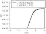
接着,图7B示出使用以算式5表示的高斯型浅缺陷态密度而算出的C-V特性与C-V特性的测量值之间的比较。从其结果可知,C-V特性的计算值与C-V特性的测量值具有高再现性。由此,作为算出浅缺陷态密度的方法,上述方法是充分妥当的。Next, FIG. 7B shows a comparison between the C-V characteristic calculated using the Gaussian shallow defect density of states expressed by
<1-5.缺陷态密度的评价><1-5. Evaluation of defect state density>
接着,通过使用在<1-4.缺陷态密度的评价方法>中说明的评价方法,对结晶性不同的氧化物半导体膜中的缺陷态密度进行评价。Next, by using the evaluation method described in <1-4. Evaluation Method of Density of Defect States>, the density of defect states in oxide semiconductor films having different crystallinity was evaluated.
《晶体管结构》"Transistor Structure"
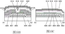
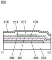
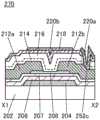
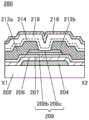
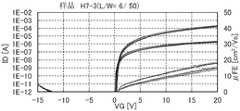
首先,参照图10A至图10C对所制造的晶体管的结构进行说明。图10A是晶体管600的俯视图,图10B是沿着图10A的点划线A1-A2的截面图,图10C是沿着图10A的点划线B1-B2的截面图。First, the structure of the fabricated transistor will be described with reference to FIGS. 10A to 10C . 10A is a plan view of the
晶体管600包括:衬底602上的用作第一栅电极的导电膜604;衬底602及导电膜604上的绝缘膜606;绝缘膜606上的绝缘膜607;绝缘膜607上的氧化物半导体膜608;与氧化物半导体膜608电连接并用作源电极的导电膜612a;以及与氧化物半导体膜608电连接并用作漏电极的导电膜612b。The
在导电膜612a、612b及氧化物半导体膜608上设置有绝缘膜614、616、618。在绝缘膜618上设置有导电膜620。绝缘膜606、607被用作第一栅极绝缘膜。绝缘膜614、616、618被用作第二栅极绝缘膜。另外,导电膜620被用作晶体管600的第二栅电极(也称为背栅电极)。On the
《晶体管的制造方法》"Manufacturing Method of Transistor"
接着,说明图10A至图10C所示的晶体管600的制造方法。首先,在衬底602上形成导电膜604。作为衬底602使用尺寸为720mm×600mm的玻璃衬底。作为导电膜604,通过使用溅射装置形成厚度为100nm的钨膜,并且将该钨膜加工为所希望的形状。Next, a method of manufacturing the
接着,在衬底602及导电膜604上形成绝缘膜606及绝缘膜607。作为绝缘膜606,通过使用PECVD装置形成厚度为400nm的氮化硅膜。作为绝缘膜607,通过使用PECVD装置形成厚度为50nm的氧氮化硅膜。Next, an insulating
接着,在绝缘膜607上形成氧化物半导体膜608。Next, an
作为氧化物半导体膜608,使用溅射装置形成厚度为35nm的IGZO膜,并且将该IGZO膜加工为所希望的形状。IGZO膜在如下条件下形成:衬底温度为170℃;将流量比为1:1的氩气体和氧气体引入处理室内;压力为0.6Pa;以及对金属氧化物溅射靶材(具有In:Ga:Zn=1:1:1.2的原子数比)供应2500W的AC功率。As the
接着,进行第一加热处理。作为该第一加热处理,在氮气气氛下以450℃进行1小时的加热处理,然后在氮与氧的混合气体气氛下以450℃进行1小时的加热处理。Next, the first heat treatment is performed. As the first heat treatment, heat treatment was performed at 450° C. for 1 hour under a nitrogen atmosphere, and then heat treatment was performed at 450° C. for 1 hour under a mixed gas atmosphere of nitrogen and oxygen.
接着,在绝缘膜607及氧化物半导体膜608上形成导电膜,在该导电膜上形成抗蚀剂掩模,对所希望的区域进行蚀刻,由此形成导电膜612a、612b。作为导电膜612a、612b,使用溅射装置在真空中连续地形成厚度为50nm的钨膜、厚度为400nm的铝膜、厚度为100nm的钛膜。在形成导电膜612a、612b之后去除抗蚀剂掩模。Next, a conductive film is formed on the insulating
接着,从绝缘膜607、氧化物半导体膜608、导电膜612a、612b的上方涂敷磷酸溶液(使用纯水稀释85%磷酸溶液100倍而成的溶液)。由此,去除不被导电膜612a、612b覆盖的氧化物半导体膜608的表面的一部分。Next, a phosphoric acid solution (a solution obtained by diluting an 85%
接着,在绝缘膜607、氧化物半导体膜608、导电膜612a、612b上形成绝缘膜614及绝缘膜616。作为绝缘膜614,通过使用PECVD装置形成厚度为50nm的氧氮化硅膜。作为绝缘膜616,通过使用PECVD装置形成厚度为400nm的氧氮化硅膜。注意,绝缘膜614及绝缘膜616通过使用PECVD装置在真空中连续地形成。Next, an insulating
绝缘膜614在如下条件下形成:衬底温度为220℃;将流量为50sccm的硅烷气体和流量为2000sccm的一氧化二氮气体引入处理室内;压力为20Pa;对设置于PECVD装置内的平行板电极之间供应100W的RF功率。绝缘膜616在如下条件下形成:衬底温度为220℃;将流量为160sccm的硅烷气体和流量为4000sccm的一氧化二氮气体引入处理室内;压力为200Pa;对设置于PECVD装置内的平行板电极之间供应1500W的RF功率。The insulating
接着,进行第二加热处理。作为该第二加热处理,在含氮的气氛下以350℃进行1小时的加热处理。Next, the second heat treatment is performed. As this second heat treatment, heat treatment was performed at 350° C. for 1 hour in a nitrogen-containing atmosphere.
接着,使用灰化装置在如下条件下对绝缘膜614、616进行氧添加处理:衬底温度为40℃;将流量为250sccm的氧气体引入处理室内;压力为15Pa;以对衬底一侧施加偏压的方式对设置于灰化装置内的平行板电极之间供应4500W的RF功率。Next, the insulating
接着,在绝缘膜616上形成绝缘膜618。作为绝缘膜618,使用PECVD装置形成厚度为100nm的氮化硅膜。绝缘膜618在如下条件下形成:衬底温度为350℃;将流量为50sccm的硅烷气体、流量为5000sccm的氮气体和流量为100sccm的氨气体引入处理室内;压力为100Pa;对设置于PECVD装置内的平行板电极之间供应1000W的RF功率。Next, an insulating
接着,在绝缘膜618上形成导电膜,且对该导电膜进行加工,来形成导电膜620。作为导电膜620,通过使用溅射装置形成厚度为100nm的ITSO膜。该ITSO膜在如下条件下形成:衬底温度为室温;将流量为72sccm的氩气体、流量为5sccm的氧气体引入处理室内;压力为0.15Pa;对设置在溅射装置内的金属氧化物靶材供应3200W的DC功率。此外,用来形成ITSO膜的金属氧化物靶材的组成为In2O3:SnO2:SiO2=85:10:5[wt%]。Next, a conductive film is formed on the insulating
接着,进行第三加热处理。作为该第三加热处理,在氮气气氛下以250℃进行1小时的加热处理。Next, the third heat treatment is performed. As this third heat treatment, heat treatment was performed at 250° C. for 1 hour in a nitrogen atmosphere.
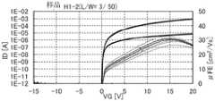
通过上述工序制造C-V特性评价用晶体管。该晶体管具有200μm的沟道长度及50μm的沟道宽度。Through the above-described steps, a transistor for evaluating C-V characteristics was produced. The transistor has a channel length of 200 μm and a channel width of 50 μm.
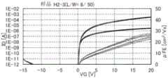
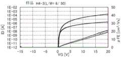
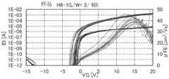
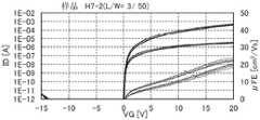
《晶体管的C-V特性的测定》《Measurement of C-V Characteristics of Transistors》
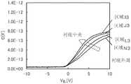
接着,对上述晶体管进行C-V特性的测定。在“Top Gate Sweep”中,将被用作第一栅电极的导电膜604电接地,并在被用作第二栅电极的导电膜620与被用作源电极及漏电极的导电膜612a、612b之间进行C-V特性的测定。在“Bottom Gate Sweep”中,将被用作第二栅电极的导电膜620电接地,并在被用作第一栅电极的导电膜604与被用作源电极及漏电极的导电膜612a、612b之间进行C-V特性的测定。Next, the measurement of the C-V characteristic of the above-mentioned transistor was performed. In "Top Gate Sweep", the
在C-V特性的测定中,对导电膜612a、612b与导电膜604或导电膜620之间在-10V至10V的范围内每隔0.2V施加电压(也称为栅极电压Vg)。作为栅极电压Vg,施加10kHz的交流电压。In the measurement of the C-V characteristics, a voltage (also referred to as gate voltage Vg) is applied between the
图11A和图11B示出上述晶体管的C-V特性的测量结果。11A and 11B show the measurement results of the C-V characteristics of the above transistors.
上述C-V特性的测量在晶体管的720mm×600mm的玻璃衬底的衬底中央附近(区域I3及J3)和衬底外周附近(区域L3及N3)进行。另外,作为玻璃衬底的坐标援用图4所示的720mm×600mm的玻璃衬底的坐标。The measurement of the above-mentioned C-V characteristics was performed in the vicinity of the substrate center (regions I3 and J3 ) and the vicinity of the substrate periphery (regions L3 and N3 ) of the 720 mm×600 mm glass substrate of the transistor. In addition, the coordinates of the glass substrate of 720 mm×600 mm shown in FIG. 4 are used as the coordinates of the glass substrate.
图11A示出Top Gate Sweep的结果,图11B示出Bottom Gate Sweep的结果。在图11A和图11B中,纵轴表示电容C,横轴表示栅极电压Vg。FIG. 11A shows the result of the Top Gate Sweep, and FIG. 11B shows the result of the Bottom Gate Sweep. In FIGS. 11A and 11B , the vertical axis represents the capacitance C, and the horizontal axis represents the gate voltage Vg.
如图11A和图11B所示,Top Gate Sweep的电容的测量值比Bottom Gate Sweep小。另外,衬底外周附近的相对于栅极电压Vg的电容的变化的测量值比衬底中央附近小。As shown in FIGS. 11A and 11B , the measured value of the capacitance of the Top Gate Sweep is smaller than that of the Bottom Gate Sweep. In addition, the measured value of the change in capacitance with respect to the gate voltage Vg in the vicinity of the outer periphery of the substrate is smaller than that in the vicinity of the center of the substrate.
《缺陷态密度》"Defective Density of States"
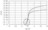
接着,通过比较C-V特性的测量值与C-V特性的计算值,算出晶体管的缺陷态密度。作为算出晶体管的缺陷态密度的方法,可以参照<1-4.缺陷态密度的评价方法>。Next, the density of defect states of the transistor is calculated by comparing the measured value of the C-V characteristic with the calculated value of the C-V characteristic. As a method of calculating the defect state density of a transistor, <1-4. Evaluation method of defect state density> can be referred to.
图12A示出对在晶体管的衬底中央附近(区域I3)使用Bottom Gate Sweep测量出的C-V特性与使用以如上所记载的算式5表示的高斯曲线(计算值)进行拟合的结果。如图12A所示,C-V特性的测量值与C-V特性的计算值通过进行拟合大致一致,由此可以算出氧化物半导体膜608中的浅缺陷态密度NSS。在图12A中,通过将N设定为2.8×1012cm-2eV-1,将W设定为0.07eV,可以对C-V特性的实测值与计算值进行拟合。也就是说,可知浅缺陷态密度的峰值N为2.8×1012cm-2eV-1。根据该曲线的积分值可以得到浅缺陷态密度(NSS)。FIG. 12A shows the result of fitting the CV characteristic measured by the Bottom Gate Sweep in the vicinity of the substrate center of the transistor (region I3 ) and the Gaussian curve (calculated value) represented by the above-described
接着,使用以如上所记载的算式5表示的高斯型浅缺陷态密度对C-V特性进行计算。图12B示出C-V特性的计算值与C-V特性的测量值的比较。从其结果可知,C-V特性的计算值与C-V特性的测量值具有高再现性。由此,作为算出浅缺陷态密度的测量方法,上述方法是充分妥当的。Next, the C-V characteristic is calculated using the Gaussian shallow defect density of states expressed by the above-described
《缺陷态密度的面内分布》"In-plane distribution of defect density of states"
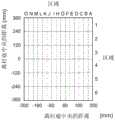
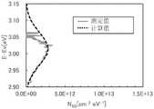
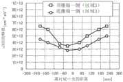
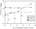
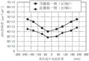
接着,为了确认720mm×600mm的玻璃衬底面内的缺陷态密度的面内分布,对区域C3、D3、F3、G3、I3、J3、L3及M3的浅缺陷态密度(也称为shallow level DOS或sDOS)的峰值进行测量。在此,作为玻璃衬底的坐标援用图4所示的720mm×600mm的玻璃衬底的坐标。图13示出720mm×600mm的玻璃衬底面内的sDOS的峰值。Next, in order to confirm the in-plane distribution of the in-plane defect state density of the glass substrate of 720 mm×600 mm, the shallow defect state density of the regions C3, D3, F3, G3, I3, J3, L3 and M3 (also called shallow level DOS or sDOS) peak value. Here, the coordinates of the glass substrate of 720 mm×600 mm shown in FIG. 4 are used as the coordinates of the glass substrate. FIG. 13 shows the peak value of sDOS in the plane of the glass substrate of 720 mm×600 mm.
如图13所示,在上述晶体管中,有sDOS从衬底中央附近增加到衬底外周附近的倾向。从此可知,该倾向与如上所记载的截面TEM图像的结晶性或者起因于尖晶石型结晶结构的XRD峰值的强度有负相关关系。As shown in FIG. 13 , in the above transistor, the sDOS tends to increase from the vicinity of the center of the substrate to the vicinity of the periphery of the substrate. From this, it can be seen that this tendency is negatively correlated with the crystallinity of the cross-sectional TEM image as described above or the intensity of the XRD peak due to the spinel-type crystal structure.
也就是说,在结晶性高的衬底中央附近sDOS小。换言之,结晶性高的氧化物半导体膜的sDOS的峰值小。That is, the sDOS is small in the vicinity of the center of the substrate with high crystallinity. In other words, the oxide semiconductor film with high crystallinity has a small peak value of sDOS.
<1-6.晶体管特性和sDOS><1-6. Transistor characteristics and sDOS>
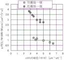
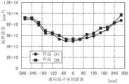
接着,对上述晶体管的特性与上述被导出的sDOS的关系进行评价。在此的晶体管特性是根据Id-Vg特性算出的场效应迁移率(μFE)。对玻璃衬底的区域C3、D3、F3、G3、I3、J3、L3及M3进行场效应迁移率(μFE)的测量。另外,作为玻璃衬底的坐标援用图4所示的720mm×600mm的玻璃衬底的坐标。Next, the relationship between the characteristics of the above-mentioned transistors and the above-derived sDOS was evaluated. The transistor characteristic here is the field effect mobility (μFE) calculated from the Id-Vg characteristic. Field effect mobility (μFE) measurements were performed on regions C3, D3, F3, G3, I3, J3, L3 and M3 of the glass substrate. In addition, the coordinates of the glass substrate of 720 mm×600 mm shown in FIG. 4 are used as the coordinates of the glass substrate.
图14示出根据晶体管的Id-Vg特性算出的场效应迁移率(μFE)与离衬底中央的距离的关系。注意,场效应迁移率(μFE)在Vd=10V的条件下进行测量。FIG. 14 shows the relationship between the field effect mobility (μFE) calculated from the Id-Vg characteristic of the transistor and the distance from the center of the substrate. Note that the field effect mobility (μFE) was measured under the condition of Vd=10V.
如图14所示,在上述晶体管中,有场效应迁移率(μFE)从衬底中央附近减少到衬底外周附近的倾向。As shown in FIG. 14 , in the above transistor, the field effect mobility (μFE) tends to decrease from the vicinity of the center of the substrate to the vicinity of the periphery of the substrate.
接着,算出图13所示的sDOS的峰值与图14所示的场效应迁移率的关系。图15示出sDOS的峰值与场效应迁移率的关系。此外,在图15中,纵轴表示场效应迁移率(μFE),横轴表示sDOS的峰值。Next, the relationship between the peak value of sDOS shown in FIG. 13 and the field effect mobility shown in FIG. 14 was calculated. FIG. 15 shows the relationship between the peak value of sDOS and the field effect mobility. In addition, in FIG. 15 , the vertical axis represents the field effect mobility (μFE), and the horizontal axis represents the peak value of sDOS.
如图15所示,当sDOS的峰值小时,有晶体管的场效应迁移率高的倾向。在进行Bottom Gate Sweep时,该倾向更显著。因此,通过包括sDOS的峰值小于1×1013cm-2eV-1,更优选小于2×1012cm-2eV-1,进一步优选小于1×1010cm-2eV-1的氧化物半导体膜,晶体管的场效应迁移率得到提高。As shown in FIG. 15 , when the peak value of sDOS is small, the field effect mobility of the transistor tends to be high. This tendency is more pronounced when performing Bottom Gate Sweep. Therefore, by including an oxide semiconductor whose peak sDOS is less than 1×1013 cm-2 eV-1 , more preferably less than 2×1012 cm-2 eV-1 , and further preferably less than 1×1010 cm-2 eV-1 film, the field effect mobility of the transistor is improved.
本实施方式所示的结构可以与其他实施方式及实施例适当地组合。The structures shown in this embodiment mode can be appropriately combined with other embodiments and examples.
实施方式2
在本实施方式中,参照图16A至图16D、图17A至图17D、图18A至图18C、图19A和图19B、图20、图21、图22A至图22C、图23A至图23F、图24A至图24G、图25A至图25G对实施方式1的氧化物半导体的详细内容进行说明。16A to 16D, 17A to 17D, 18A to 18C, 19A and 19B, 20, 21, 22A to 22C, 23A to 23F, 24A to 24G and 25A to 25G describe the details of the oxide semiconductor of the first embodiment.
<2-1.CAAC-OS><2-1.CAAC-OS>
首先,对CAAC-OS进行说明。First, CAAC-OS will be described.
CAAC-OS是包含多个c轴取向的结晶部(也称为颗粒)的氧化物半导体之一。CAAC-OS is one of oxide semiconductors including a plurality of c-axis-oriented crystal parts (also referred to as particles).
在利用TEM观察所得到的CAAC-OS的明视场图像与衍射图案的复合分析图像(也称为高分辨率TEM图像)中,观察到多个颗粒。然而,在高分辨率TEM图像中,观察不到颗粒与颗粒之间的明确的边界,即晶界(grain boundary)。因此,在CAAC-OS中,不容易发生起因于晶界的电子迁移率的降低。In a composite analysis image (also referred to as a high-resolution TEM image) of a bright-field image of CAAC-OS and a diffraction pattern obtained by TEM observation, a plurality of particles were observed. However, in high-resolution TEM images, clear boundaries between particles, ie, grain boundaries, are not observed. Therefore, in CAAC-OS, the decrease in electron mobility due to grain boundaries does not easily occur.
下面,对利用TEM观察的CAAC-OS进行说明。图16A示出从大致平行于样品面的方向观察所得到的CAAC-OS的截面的高分辨率TEM图像。利用球面像差校正(sphericalaberration corrector)功能得到高分辨率TEM图像。将利用球面像差校正功能所得到的高分辨率TEM图像特别称为Cs校正高分辨率TEM图像。例如,可以使用日本电子株式会社制造的原子分辨率分析型电子显微镜JEM-ARM200F得到Cs校正高分辨率TEM图像。Next, CAAC-OS observed by TEM will be described. FIG. 16A shows a high-resolution TEM image of a cross-section of the obtained CAAC-OS viewed from a direction approximately parallel to the sample surface. High-resolution TEM images were obtained using the spherical aberration corrector function. The high-resolution TEM image obtained by utilizing the spherical aberration correction function is particularly referred to as a Cs-corrected high-resolution TEM image. For example, a Cs-corrected high-resolution TEM image can be obtained using an atomic resolution analytical electron microscope JEM-ARM200F manufactured by JEOL Ltd.
图16B是图16A中的区域(1)的放大Cs校正高分辨率TEM图像。图16B示出在颗粒中金属原子排列为层状。各金属原子层具有反映了形成CAAC-OS膜的面(下面,将该面也称为形成面)或CAAC-OS膜的顶面的凸凹的配置,并以平行于CAAC-OS膜的形成面或顶面的方式排列。Figure 16B is an enlarged Cs-corrected high-resolution TEM image of region (1) in Figure 16A. Figure 16B shows that the metal atoms are arranged in layers in the particle. Each metal atomic layer has a configuration reflecting the unevenness of the surface on which the CAAC-OS film is formed (hereinafter, this surface is also referred to as the formation surface) or the top surface of the CAAC-OS film, and is parallel to the formation surface of the CAAC-OS film. Or the way to arrange the top surface.
如图16B所示,CAAC-OS具有特有的原子排列。在图16C中以辅助线示出特有的原子排列。由图16B和图16C可知,颗粒的尺寸为1nm至3nm左右,由颗粒与颗粒之间的倾斜产生的空隙的尺寸为0.8nm左右。因此,也可以将颗粒称为纳米晶(nc:nanocrystal)。另外,可以将CAAC-OS称为具有CANC(c-axis aligned nanocrystals:c轴取向纳米晶)的氧化物半导体。As shown in Figure 16B, CAAC-OS has a characteristic atomic arrangement. The characteristic atomic arrangement is shown with auxiliary lines in Figure 16C. As can be seen from FIGS. 16B and 16C , the size of the particles is about 1 nm to 3 nm, and the size of the voids generated by the inclination between the particles is about 0.8 nm. Therefore, the particles may also be referred to as nanocrystals (nc: nanocrystals). In addition, CAAC-OS can be referred to as an oxide semiconductor with CANC (c-axis aligned nanocrystals: c-axis aligned nanocrystals).
在此,根据Cs校正高分辨率TEM图像,将衬底5120上的CAAC-OS的颗粒5100的配置示意性地表示为堆积砖块或块体的结构(参照图16D)。在图16C中观察到的在颗粒与颗粒之间产生倾斜的部分相当于图16D所示的区域5161。Here, the arrangement of the
图17A示出从大致垂直于样品面的方向观察所得到的CAAC-OS的平面的Cs校正高分辨率TEM图像。图17B、图17C和图17D分别是图17A中的区域(1)、区域(2)和区域(3)的放大Cs校正高分辨率TEM图像。由图17B、图17C和图17D可知,在颗粒中金属原子排列为三角形状、四角形状或六角形状。但是,在不同的颗粒之间金属原子的排列没有规律性。FIG. 17A shows a Cs-corrected high-resolution TEM image of the plane of the resulting CAAC-OS viewed from a direction approximately perpendicular to the sample plane. Figures 17B, 17C, and 17D are magnified Cs-corrected high-resolution TEM images of region (1), region (2), and region (3) in Figure 17A, respectively. As can be seen from FIGS. 17B , 17C and 17D , the metal atoms are arranged in a triangular shape, a quadrangular shape or a hexagonal shape in the particles. However, there is no regularity in the arrangement of metal atoms between different particles.
接着,说明通过XRD进行分析的CAAC-OS。例如,当利用out-of-plane法分析包含InGaZnO4结晶的CAAC-OS的结构时,如图18A所示,在衍射角(2θ)为31°附近时出现峰值。该峰值来源于InGaZnO4结晶的(009)面,由此可知CAAC-OS中的结晶具有c轴取向性,并且c轴朝向大致垂直于CAAC-OS的形成面或顶面的方向。Next, CAAC-OS analyzed by XRD will be described. For example, when the structure of CAAC-OS including InGaZnO4 crystals is analyzed by the out-of-plane method, as shown in FIG. 18A , a peak appears when the diffraction angle (2θ) is around 31°. This peak is derived from the (009) plane of the InGaZnO4 crystal, and it can be seen that the crystal in CAAC-OS has c-axis orientation, and the c-axis is oriented in a direction substantially perpendicular to the formation surface or top surface of CAAC-OS.
注意,当利用out-of-plane法分析CAAC-OS的结构时,除了2θ为31°附近的峰值以外,在2θ为36°附近时也出现峰值。2θ为36°附近的峰值表示CAAC-OS中的一部分包含不具有c轴取向性的结晶。优选的是,在利用out-of-plane法分析的CAAC-OS的结构中,在2θ为31°附近时出现峰值而在2θ为36°附近时不出现峰值。Note that when the structure of CAAC-OS was analyzed by the out-of-plane method, in addition to the peak around 31° in 2θ, a peak appeared around 36° in 2θ. The peak near 36° in 2θ indicates that a part of CAAC-OS contains crystals that do not have c-axis orientation. Preferably, in the structure of CAAC-OS analyzed by the out-of-plane method, the peak appears when 2θ is around 31° and the peak does not appear when 2θ is around 36°.
另一方面,当利用从大致垂直于c轴的方向使X射线入射到样品的in-plane法分析CAAC-OS的结构时,在2θ为56°附近时出现峰值。该峰值来源于InGaZnO4结晶的(110)面。在CAAC-OS中,当将2θ固定为56°附近并在以样品面的法线向量为轴(φ轴)旋转样品的条件下进行分析(φ扫描)时,如图18B所示的那样观察不到明确的峰值。相比之下,在InGaZnO4的单晶氧化物半导体中,在将2θ固定为56°附近来进行φ扫描时,如图18C所示的那样观察到来源于相等于(110)面的结晶面的六个峰值。因此,由使用XRD的结构分析确认到CAAC-OS中的a轴和b轴的取向没有规律性。On the other hand, when the structure of CAAC-OS is analyzed by the in-plane method in which X-rays are incident on the sample from a direction substantially perpendicular to the c-axis, a peak appears when 2θ is around 56°. This peak originates from the (110) plane of the InGaZnO4 crystal. In CAAC-OS, when 2θ is fixed around 56° and the sample is rotated with the normal vector of the sample surface as the axis (φ axis), the analysis (φ scan) is performed, as shown in FIG. 18B . less than a clear peak. In contrast, in the single crystal oxide semiconductor of InGaZnO4 , when φ scan was performed with 2θ fixed at around 56°, a crystal plane derived from the (110) plane was observed as shown in FIG. 18C . of six peaks. Therefore, it was confirmed from the structural analysis using XRD that the orientations of the a-axis and the b-axis in CAAC-OS had no regularity.
接着,说明利用电子衍射进行分析的CAAC-OS。例如,当对包含InGaZnO4结晶的CAAC-OS在平行于样品面的方向上入射束径为300nm的电子束时,可以获得图19A所示的衍射图案(也称为选区透射电子衍射图案)。在该衍射图案中包含起因于InGaZnO4结晶的(009)面的斑点。因此,由电子衍射也可知CAAC-OS所包含的颗粒具有c轴取向性,并且c轴朝向大致垂直于CAAC-OS的形成面或顶面的方向。另一方面,图19B示出对相同的样品在垂直于样品面的方向上入射束径为300nm的电子束时的衍射图案。如图19B所示,观察到环状的衍射图案。因此,由电子衍射也可知CAAC-OS所包含的颗粒的a轴和b轴不具有取向性。可以认为图19B中的第一环起因于InGaZnO4结晶的(010)面和(100)面等。另外,可以认为图19B中的第二环起因于(110)面等。Next, CAAC-OS analyzed by electron diffraction will be described. For example, when an electron beam with a beam diameter of 300 nm is incident on CAAC- OS containing InGaZnO crystals in a direction parallel to the sample surface, a diffraction pattern (also referred to as a selected area transmission electron diffraction pattern) shown in FIG. 19A can be obtained. The diffraction pattern includes spots originating from the (009) plane of the InGaZnO4 crystal. Therefore, it can be seen from electron diffraction that the particles contained in the CAAC-OS have c-axis orientation, and the c-axis is oriented in a direction substantially perpendicular to the formation surface or the top surface of the CAAC-OS. On the other hand, FIG. 19B shows a diffraction pattern when an electron beam having a beam diameter of 300 nm is incident on the same sample in a direction perpendicular to the sample surface. As shown in Fig. 19B, a ring-shaped diffraction pattern was observed. Therefore, the a-axis and b-axis of the particle|grains contained in CAAC-OS have no orientation property also from electron diffraction. It is considered that the first ring in FIG. 19B originates from the (010) plane, the (100) plane, and the like of the InGaZnO4 crystal. In addition, it is considered that the second loop in FIG. 19B originates from the (110) plane or the like.
如上所述,CAAC-OS是结晶性高的氧化物半导体。氧化物半导体的结晶性有时因杂质的混入或缺陷的生成等而降低。这意味着,CAAC-OS的杂质及缺陷(例如,氧缺陷)少。As described above, CAAC-OS is an oxide semiconductor with high crystallinity. The crystallinity of an oxide semiconductor may be lowered due to contamination of impurities, generation of defects, or the like. This means that the impurities and defects (eg, oxygen defects) of the CAAC-OS are small.
此外,杂质是指氧化物半导体的主要成分以外的元素,诸如氢、碳、硅和过渡金属元素。例如,与氧的键合力比包含在氧化物半导体中的金属元素强的元素(具体而言,硅等)会从氧化物半导体夺取氧,由此打乱氧化物半导体的原子排列,导致其结晶性下降。由于铁或镍等的重金属、氩、二氧化碳等的原子半径(或分子半径)大,所以会打乱氧化物半导体的原子排列,导致结晶性下降。Further, impurities refer to elements other than the main components of the oxide semiconductor, such as hydrogen, carbon, silicon, and transition metal elements. For example, an element (specifically, silicon, etc.) having a stronger bonding force with oxygen than a metal element contained in an oxide semiconductor takes oxygen from the oxide semiconductor, thereby disrupting the atomic arrangement of the oxide semiconductor, causing it to crystallize Sexual decline. Heavy metals such as iron and nickel, argon, carbon dioxide, and the like have large atomic radii (or molecular radii), so that the atomic arrangement of the oxide semiconductor is disturbed, resulting in a decrease in crystallinity.
包含杂质或缺陷的氧化物半导体的特性有时因光或热等会发生变动。例如,包含于氧化物半导体的杂质有时会成为载流子陷阱或载流子发生源。另外,氧化物半导体中的氧缺陷有时会成为载流子陷阱或者当其中俘获氢时成为载流子发生源。The properties of an oxide semiconductor containing impurities or defects may vary due to light, heat, or the like. For example, impurities contained in an oxide semiconductor may become a carrier trap or a carrier generation source. In addition, oxygen vacancies in oxide semiconductors sometimes become carrier traps or become a carrier generation source when hydrogen is trapped therein.
杂质及氧缺陷少的CAAC-OS是载流子密度低(具体而言,小于8×10¹¹/cm3,优选小于1×1011/cm3,更优选小于1×1010/cm3,且是1×10-9/cm3以上)的氧化物半导体。将这样的氧化物半导体称为高纯度本征或实质上高纯度本征的氧化物半导体。CAAC-OS的杂质浓度和缺陷态密度低。因此,可以将CAAC-OS称为具有稳定特性的氧化物半导体。CAAC-OS with few impurities and oxygen defects has a low carrier density (specifically, less than 8×10¹¹ /cm3 , preferably less than 1×10¹¹ /cm3 , more preferably less than 1×10¹⁰ /cm3 , and 1×10⁻⁹ /cm3 or more) oxide semiconductor. Such an oxide semiconductor is called a high-purity intrinsic or substantially high-purity intrinsic oxide semiconductor. The impurity concentration and defect state density of CAAC-OS are low. Therefore, CAAC-OS can be called an oxide semiconductor with stable characteristics.
<2-2.nc-OS><2-2.nc-OS>
接着说明nc-OS。Next, nc-OS will be described.
nc-OS在高分辨率TEM图像中有能够观察到结晶部的区域和观察不到明确的结晶部的区域。nc-OS所包含的结晶部的尺寸大多为1nm以上且10nm以下或1nm以上且3nm以下。注意,有时将其结晶部的尺寸大于10nm且是100nm以下的氧化物半导体称为微晶氧化物半导体。例如,在nc-OS的高分辨率TEM图像中,有时无法明确地观察到晶界。注意,纳米晶的来源有可能与CAAC-OS中的颗粒相同。因此,下面有时将nc-OS的结晶部称为颗粒。In the high-resolution TEM image of nc-OS, there are regions where crystal parts can be observed and regions where clear crystal parts are not observed. The size of the crystal part included in nc-OS is often 1 nm or more and 10 nm or less, or 1 nm or more and 3 nm or less. Note that an oxide semiconductor whose crystal portion size is larger than 10 nm and 100 nm or less may be referred to as a microcrystalline oxide semiconductor. For example, in high-resolution TEM images of nc-OS, grain boundaries are sometimes not clearly observed. Note that it is possible that the source of nanocrystals is the same as the particles in CAAC-OS. Therefore, the crystal part of nc-OS is sometimes referred to as a particle below.
在nc-OS中,微小的区域(例如1nm以上且10nm以下的区域,特别是1nm以上且3nm以下的区域)中的原子排列具有周期性。在nc-OS的不同颗粒之间观察不到结晶取向的规律性。因此,在膜整体中观察不到取向性。所以,根据分析方法有时nc-OS与a-like OS或非晶氧化物半导体没有差别。例如,当利用使用其束径比颗粒大的X射线的out-of-plane法对nc-OS进行分析时,检测不到表示结晶面的峰值。在使用其束径比颗粒大(例如,50nm以上)的电子射线对nc-OS进行电子衍射时,观察到类似光晕图案的衍射图案。另一方面,在照射其束径近于颗粒或者比颗粒小的电子射线时,在nc-OS的纳米束电子衍射图案中观察到斑点。另外,在nc-OS的纳米束电子衍射图案中,有时观察到圆圈状(环状)的亮度高的区域。而且,在nc-OS的纳米束电子衍射图案中,有时观察到环状的区域内的多个斑点。In nc-OS, the atomic arrangement in a minute region (for example, a region of 1 nm or more and 10 nm or less, in particular, a region of 1 nm or more and 3 nm or less) has periodicity. No regularity of crystallographic orientation was observed between different particles of nc-OS. Therefore, no orientation was observed in the entire film. Therefore, depending on the analysis method, there may be no difference between nc-OS and a-like OS or amorphous oxide semiconductor. For example, when nc-OS is analyzed by the out-of-plane method using X-rays whose beam diameter is larger than that of particles, no peaks indicating crystal planes are detected. When the nc-OS is electron-diffracted using electron rays whose beam diameter is larger than that of the particles (eg, 50 nm or more), a diffraction pattern resembling a halo pattern is observed. On the other hand, when an electron beam whose beam diameter is close to or smaller than that of the particles is irradiated, spots are observed in the nanobeam electron diffraction pattern of nc-OS. In addition, in the nanobeam electron diffraction pattern of nc-OS, a circle-shaped (annular) region with high brightness may be observed. Furthermore, in the nanobeam electron diffraction pattern of nc-OS, a plurality of spots in a ring-shaped region may be observed.
如此,由于在颗粒(纳米晶)之间结晶取向都没有规律性,所以也可以将nc-OS称为包含RANC(random aligned nanocrystals:无规取向纳米晶)的氧化物半导体或包含NANC(non-aligned nanocrystals:无取向纳米晶)的氧化物半导体。In this way, since there is no regularity in the crystallographic orientation between particles (nanocrystals), nc-OS can also be called an oxide semiconductor containing RANC (random aligned nanocrystals) or an oxide semiconductor containing NANC (non- aligned nanocrystals: non-aligned nanocrystals) oxide semiconductors.
nc-OS是规律性比非晶氧化物半导体高的氧化物半导体。因此,nc-OS的缺陷态密度比a-like OS及非晶氧化物半导体低。注意,在nc-OS中的不同的颗粒之间观察不到晶体取向的规律性。所以,nc-OS的缺陷态密度比CAAC-OS高。nc-OS is an oxide semiconductor with higher regularity than an amorphous oxide semiconductor. Therefore, the defect state density of nc-OS is lower than that of a-like OS and amorphous oxide semiconductors. Note that no regularity of crystallographic orientation is observed between different particles in nc-OS. Therefore, the defect state density of nc-OS is higher than that of CAAC-OS.
<2-3.a-like OS><2-3.a-like OS>
a-like OS具有介于nc-OS与非晶氧化物半导体之间的结构。a-like OS has a structure intermediate between nc-OS and amorphous oxide semiconductor.
在a-like OS的高分辨率TEM图像中,有时观察到空洞。另外,在高分辨率TEM图像中,有明确地观察到结晶部的区域和观察不到结晶部的区域。In high-resolution TEM images of a-like OS, voids are sometimes observed. In addition, in the high-resolution TEM image, there are regions where crystal parts are clearly observed and regions where crystal parts are not observed.
由于a-like OS包含空洞,所以其具有不稳定结构。为了证明与CAAC-OS及nc-OS相比a-like OS具有不稳定的结构,下面示出电子照射所导致的结构变化。Since a-like OS contains voids, it has an unstable structure. In order to demonstrate that a-like OS has an unstable structure compared with CAAC-OS and nc-OS, the structural change by electron irradiation is shown below.
作为进行电子照射的样品,准备a-like OS(记载为样品A)、nc-OS(记载为样品B)和CAAC-OS(记载为样品C)。每个样品都是In-Ga-Zn氧化物。As samples for electron irradiation, a-like OS (described as sample A), nc-OS (described as sample B), and CAAC-OS (described as sample C) were prepared. Each sample is In-Ga-Zn oxide.
首先,取得各样品的高分辨率截面TEM图像。由高分辨率截面TEM图像可知,所有样品都具有结晶部。First, a high-resolution cross-sectional TEM image of each sample is acquired. From the high-resolution cross-sectional TEM images, it was found that all the samples had crystal parts.
注意,如下那样决定将哪个部分作为结晶部。已知InGaZnO4结晶的单位晶格具有包括三个In-O层和六个Ga-Zn-O层的九个层在c轴方向上以层状层叠的结构。这些彼此靠近的层的间隔与(009)面的晶格表面间隔(也称为d值)是相等的。由结晶结构分析求出其值为0.29nm。由此,可以将晶格条纹的间隔为0.28nm以上且0.30nm以下的部分作为InGaZnO4结晶部。每个晶格条纹对应于InGaZnO4结晶的a-b面。Note that which part is to be the crystal part is determined as follows. It is known that the unit lattice of the InGaZnO4 crystal has a structure in which nine layers including three In-O layers and six Ga-Zn-O layers are stacked in layers in the c-axis direction. The spacing of these adjacent layers is equal to the lattice surface spacing of the (009) plane (also referred to as the d value). The value was found to be 0.29 nm from the crystal structure analysis. Thereby, the part where the interval of the lattice fringes is 0.28 nm or more and 0.30 nm or less can be used as the InGaZnO4 crystal part. Each lattice fringe corresponds to the ab plane of theInGaZnO crystal.
图20示出各样品的结晶部(22个部分至45个部分)的平均尺寸的变化。注意,结晶部尺寸对应于上述晶格条纹的长度。由图20可知,在a-like OS中,结晶部根据电子的累积照射量逐渐变大。具体而言,如图20中的(1)所示,在TEM观察初期的尺寸为1.2nm左右的结晶部(也称为初始晶核)在累积照射量为4.2×10⁸e-/nm2时生长到2.6nm左右。另一方面,可知nc-OS和CAAC-OS在开始电子照射时到电子的累积照射量为4.2×108e-/nm2的期间,结晶部的尺寸都没有变化。具体而言,如图20中的(2)及(3)所示,无论电子的累积照射量如何,nc-OS及CAAC-OS的平均结晶部尺寸都分别为1.4nm左右及2.1nm左右。FIG. 20 shows the change in the average size of the crystal parts (22 parts to 45 parts) of each sample. Note that the crystal portion size corresponds to the length of the above-described lattice fringes. As can be seen from FIG. 20 , in the a-like OS, the crystal portion gradually increases according to the cumulative irradiation amount of electrons. Specifically, as shown in (1) in FIG. 20 , the crystal portion (also referred to as an initial crystal nucleus) having a size of about 1.2 nm in the initial stage of TEM observation was 4.2×10⁸ e− /nm2 at the cumulative irradiation dose. grow to about 2.6 nm. On the other hand, in both nc-OS and CAAC-OS, it was found that the size of the crystal portion did not change until the cumulative irradiation dose of electrons was 4.2×10⁸ e− /nm2 when the electron irradiation was started. Specifically, as shown in (2) and (3) of FIG. 20 , regardless of the cumulative irradiation amount of electrons, the average crystal size of nc-OS and CAAC-OS was about 1.4 nm and about 2.1 nm, respectively.
如此,有时电子照射引起a-like OS中的结晶部的生长。另一方面,在nc-OS和CAAC-OS中,几乎没有电子照射所引起的结晶部的生长。因此,a-like OS与CAAC-OS及nc-OS相比具有不稳定的结构。In this way, the electron irradiation sometimes causes the growth of crystal parts in the a-like OS. On the other hand, in nc-OS and CAAC-OS, there is almost no growth of crystal parts by electron irradiation. Therefore, a-like OS has an unstable structure compared to CAAC-OS and nc-OS.
由于a-like OS包含空洞,所以其密度比nc-OS及CAAC-OS低。具体地,a-like OS的密度为具有相同组成的单晶氧化物半导体的78.6%以上且小于92.3%。nc-OS及CAAC-OS的密度为具有相同组成的单晶氧化物半导体的92.3%以上且小于100%。注意,难以形成其密度小于单晶氧化物半导体的密度的78%的氧化物半导体。Since a-like OS contains voids, its density is lower than that of nc-OS and CAAC-OS. Specifically, the density of the a-like OS is 78.6% or more and less than 92.3% of the single crystal oxide semiconductor having the same composition. The densities of nc-OS and CAAC-OS are 92.3% or more and less than 100% of the single crystal oxide semiconductors having the same composition. Note that it is difficult to form an oxide semiconductor whose density is less than 78% of that of a single crystal oxide semiconductor.
例如,在原子数比为In:Ga:Zn=1:1:1的氧化物半导体中,具有菱方晶系结构的单晶InGaZnO4的密度为6.357g/cm3。因此,例如,在原子数比为In:Ga:Zn=1:1:1的氧化物半导体中,a-like OS的密度为5.0g/cm3以上且小于5.9g/cm3。例如,在原子数比为In:Ga:Zn=1:1:1的氧化物半导体中,nc-OS和CAAC-OS的密度为5.9g/cm3以上且小于6.3g/cm3。For example, in an oxide semiconductor having an atomic ratio of In:Ga:Zn=1:1:1, the density of single crystal InGaZnO4 having a rhombohedral structure is 6.357 g/cm3 . Therefore, for example, in an oxide semiconductor having an atomic ratio of In:Ga:Zn=1:1:1, the density of a-like OS is 5.0 g/cm3 or more and less than 5.9 g/cm3 . For example, in an oxide semiconductor having an atomic ratio of In:Ga:Zn=1:1:1, the densities of nc-OS and CAAC-OS are 5.9 g/cm3 or more and less than 6.3 g/cm3 .
注意,有可能不存在相同组成的单晶氧化物半导体。此时,通过以任意比例组合组成不同的单晶氧化物半导体,可以估计出相当于所希望的组成的单晶氧化物半导体的密度。根据组成不同的单晶氧化物半导体的组合比例使用加权平均计可以算出具有所希望的组成的单晶氧化物半导体的密度。注意,优选尽可能减少所组合的单晶氧化物半导体的种类来计算密度。Note that there is a possibility that a single crystal oxide semiconductor of the same composition does not exist. At this time, by combining the single crystal oxide semiconductors of different compositions in an arbitrary ratio, the density of the single crystal oxide semiconductors corresponding to the desired composition can be estimated. The density of a single crystal oxide semiconductor having a desired composition can be calculated using a weighted average calculation from the combination ratio of the single crystal oxide semiconductors having different compositions. Note that it is preferable to calculate the density by reducing the types of single crystal oxide semiconductors to be combined as much as possible.
如上所述,氧化物半导体具有各种结构及各种特性。注意,氧化物半导体例如可以是包括非晶氧化物半导体、a-like OS、nc-OS和CAAC-OS中的两种以上的叠层。As described above, oxide semiconductors have various structures and various properties. Note that the oxide semiconductor may be, for example, a stacked layer including two or more of amorphous oxide semiconductor, a-like OS, nc-OS, and CAAC-OS.
<2-4.CAAC-OS膜的形成方法><2-4. Formation method of CAAC-OS film>
下面,对CAAC-OS膜的形成方法的一个例子进行说明。Next, an example of the formation method of the CAAC-OS film will be described.
图21是成膜室内的示意图。CAAC-OS膜可以利用溅射法形成。FIG. 21 is a schematic view of a film-forming chamber. The CAAC-OS film can be formed by sputtering.
如图21所示,衬底5220与靶材5230彼此相对地配置。在衬底5220与靶材5230之间产生等离子体5240。在衬底5220下部有加热机构5260。靶材5230被贴合到垫板上(未图示)。在隔着垫板与靶材5230相对的位置配置有多个磁铁。利用磁铁的磁场提高成膜速度的溅射法被称为磁控溅射法。As shown in FIG. 21 , the
衬底5220与靶材5230的距离d(也称为靶材与衬底之间的距离(T-S间距离))为0.01m以上且1m以下,优选为0.02m以上且0.5m以下。成膜室内几乎被成膜气体(例如,氧气体、氩气体或包含5vol%以上的氧的混合气体)充满,并且成膜室内的压力被控制为0.01Pa以上且100Pa以下,优选为0.1Pa以上且10Pa以下。在此,通过对靶材5230施加一定程度以上的电压来开始放电,且确认到等离子体5240。由磁场在靶材5230附近形成高密度等离子体区域。在高密度等离子体区域中,成膜气体离子化而产生离子5201。作为离子5201的例子,有氧的阳离子(O+)及氩的阳离子(Ar+)。The distance d between the
在此,靶材5230具有包括多个晶粒的多晶结构,其中任一个晶粒中有劈开面。作为一个例子,图22A至图22C示出靶材5230所包含的InMZnO4(元素M例如是Al、Ga、Y或Sn)的结晶结构。图22A示出从平行于b轴的方向观察时的InMZnO4的结晶结构。在InMZnO4结晶中,氧原子具有负电荷,由此在靠近的两个M-Zn-O层之间产生斥力。因此,InMZnO4结晶在靠近的两个M-Zn-O层之间具有劈开面。Here, the
在高密度等离子体区域产生的离子5201由电场向靶材5230一侧被加速而碰撞到靶材5230。此时,平板状或颗粒状的溅射粒子的颗粒5200从劈开面剥离(图21)。颗粒5200位于图22A所示的两个劈开面之间。因此,当观察颗粒5200时,其截面成为如图22B所示的那样,其顶面成为如图22C所示的那样。另外,颗粒5200的结构有时会因离子5201碰撞的冲击而产生畸变。The ions 5201 generated in the high-density plasma region are accelerated toward the
颗粒5200是具有三角形(例如正三角形)的平面的平板状(颗粒状)的溅射粒子。或者,颗粒5200是具有六角形(例如正六角形)的平面的平板状(颗粒状)的溅射粒子。注意,颗粒5200的平面形状不局限于三角形或六角形。例如,有时该平面为组合多个三角形的形状。例如,有时也成为组合两个三角形(例如,正三角形)而成的四角形(例如,菱形)。The
颗粒5200的厚度取决于成膜气体的种类等。例如,颗粒5200的厚度为0.4nm以上且1nm以下,优选为0.6nm以上且0.8nm以下。另外,例如,颗粒5200的宽度为1nm以上且100nm以下,优选为2nm以上且50nm以下,更优选为3nm以上且30nm以下。例如,使离子5201碰撞到具有In-M-Zn氧化物的靶材5230。然后,具有M-Zn-O层、In-O层及M-Zn-O层这三层的颗粒5200剥离。此外,随着颗粒5200的剥离,粒子5203也从靶材5230被弹出。粒子5203具有一个原子或几个原子的集合体。由此,可以将该粒子5203称为原子状粒子(atomic particle)。The thickness of the
颗粒5200有时在经过等离子体5240时接收电荷,而其表面带负电或正电。例如,颗粒5200从等离子体5240中的O2-接收负电荷。其结果是,有时颗粒5200的表面的氧原子带负电。此外,颗粒5200有时在经过等离子体5240时,通过与等离子体5240中的铟、元素M、锌或氧等键合而生长。
经过等离子体5240的颗粒5200及粒子5203到达衬底5220的表面。此外,粒子5203的一部分由于质量小所以有时通过真空泵等排出到外部。The
接着,参照图23A至图23F说明在衬底5220的表面上沉积的颗粒5200及粒子5203。Next, the
首先,第一个颗粒5200沉积在衬底5220上。由于颗粒5200是平板状,所以以其平面朝向衬底5220的表面的方式沉积。此时,颗粒5200的衬底5220一侧的表面上的电荷穿过衬底5220释放。First, a
接着,第二个颗粒5200到达衬底5220。由于第一颗粒5200的表面及第二个颗粒5200的表面带电荷,所以互相排斥。其结果是,第二个颗粒5200避开第一颗粒5200上,而在衬底5220的表面的离第一个颗粒5200较远的部分以其平面朝向衬底5220的表面的方式沉积。通过反复进行上述步骤,在衬底5220的表面沉积无数个颗粒5200,该沉积的厚度为一层。在颗粒5200之间产生未沉积颗粒5200的区域(参照图23A)。Next, the
接着,从等离子体接收能量的粒子5203到达衬底5220的表面。粒子5203不能沉积在颗粒5200的表面等活性区域上。由此,粒子5203移动到未沉积颗粒5200的区域并附着于颗粒5200的侧面。由于粒子5203的键通过从等离子体接收能量而处于活性状态,所以该粒子5203在化学上与颗粒5200键合而形成横向生长部5202(参照图23B)。Next, the
接着,横向生长部5202在横向方向上生长,由此颗粒5200彼此连接(参照图23C)。如此,横向生长部5202形成到填满未沉积颗粒5200的区域为止。该机理类似于原子层沉积(ALD:atomic layer deposition)法的沉积机理。Next, the
即使颗粒5200朝向彼此不同的方向,粒子5203也横向生长来填入颗粒5200间,因此不形成明确的晶界。此外,由于在颗粒5200间粒子5203平滑地连接,所以形成与单晶及多晶都不同的结晶结构。换言之,形成在微小的结晶区域(颗粒5200)间具有应变的结晶结构。填入结晶区域间的区域为具有应变的结晶区域,由此将该区域称为非晶结构是不宜的。Even if the
接着,其他的颗粒5200以平面朝向衬底5220的表面的方式沉积(参照图23D)。然后,粒子5203以填入未沉积颗粒5200的区域的方式沉积而形成横向生长部5202(参照图23E)。如此,粒子5203附着于颗粒5200的侧面,横向生长部5202在横向方向上生长,而使第二层中的颗粒5200彼此连接(参照图23F)。成膜直到形成第m层(m为二以上的整数)为止进行。其结果是,形成包含叠层体的薄膜结构。Next,
颗粒5200的沉积机理根据衬底5220的表面温度等而变化。例如,若衬底5220的表面温度较高,颗粒5200的迁移则在衬底5220的表面上发生。其结果是,由于颗粒5200之间直接连接而不夹着粒子5203的比例增加,所以成为取向性高的CAAC-OS。在形成CAAC-OS时的衬底5220的表面温度为室温以上且低于340℃,优选为室温以上且300℃以下,更优选为100℃以上且250℃以下,进一步优选为100℃以上且200℃以下。因此,即使作为衬底5220使用第八代以上的大面积衬底,也几乎不产生CAAC-OS的成膜所引起的翘曲等。The deposition mechanism of the
另一方面,若衬底5220的表面温度较低,颗粒5200的迁移则在衬底5220的表面上不容易发生。其结果是,颗粒5200沉积而形成取向性低的nc-OS等。在nc-OS中,由于颗粒5200带负电,有可能颗粒5200以彼此隔有一定间隔的方式沉积。因此,虽然nc-OS的取向性较低,但因其略有规律性,所以与非晶氧化物半导体相比具有致密的结构。On the other hand, if the surface temperature of the
当在CAAC-OS中颗粒彼此之间的间隙极小时,有时颗粒形成大颗粒。在大颗粒内具有单晶结构。例如,从顶面看时,颗粒的尺寸有时为10nm以上且200nm以下、15nm以上且100nm以下或20nm以上且50nm以下。When the gaps between particles in CAAC-OS are extremely small, the particles sometimes form large particles. It has a single crystal structure within the large particles. For example, when viewed from the top surface, the particle size may be 10 nm or more and 200 nm or less, 15 nm or more and 100 nm or less, or 20 nm or more and 50 nm or less.
如上述成膜模型那样,可以认为颗粒沉积于衬底的表面。即使形成面不具有结晶结构,也能够形成CAAC-OS。因此,可知作为与外延生长不同的上述成膜模型是很妥当的。此外,借助于上述成膜模型,在大面积的玻璃衬底等上也能够均匀地形成CAAC-OS膜或nc-OS膜。例如,即使衬底表面(形成面)具有非晶结构(例如,非晶氧化硅),也能够形成CAAC-OS。As in the above-mentioned film formation model, it can be considered that the particles are deposited on the surface of the substrate. CAAC-OS can be formed even if the formation surface does not have a crystalline structure. Therefore, it turned out that it is suitable as the above-mentioned film formation model different from epitaxial growth. Furthermore, by means of the above-described film formation model, the CAAC-OS film or the nc-OS film can be uniformly formed even on a large-area glass substrate or the like. For example, CAAC-OS can be formed even if the substrate surface (formation surface) has an amorphous structure (eg, amorphous silicon oxide).
此外,即使在衬底表面(形成面)为凹凸状的情况下,颗粒也沿着其形状排列。Furthermore, even when the substrate surface (formation surface) is uneven, the particles are arranged along the shape.
根据上述成膜模型可知,通过如下方法可以形成结晶性高的CAAC-OS:为了增加平均自由程而在更高真空状态下进行成膜;为了减少衬底附近的损伤而减弱等离子体的能量;对形成面施加热能,以恢复因进行成膜时的等离子体导致的损伤。According to the above film formation model, CAAC-OS with high crystallinity can be formed by the following methods: film formation in a higher vacuum state in order to increase the mean free path; in order to reduce the damage near the substrate, the energy of the plasma is weakened; Thermal energy is applied to the formation surface to recover damage caused by plasma during film formation.
上述成膜模型不局限于使用如下靶材,即具有含有多个晶粒的In-M-Zn氧化物等复合氧化物的多晶结构且其中任一晶粒包含劈开面的靶材的情况。例如,也可以应用于使用含有氧化铟、元素M的氧化物以及氧化锌的混合物靶材的情况。The above-mentioned film formation model is not limited to the use of a target that has a polycrystalline structure of a composite oxide such as In-M-Zn oxide containing a plurality of crystal grains and any one of the crystal grains includes a cleavage surface. . For example, it can also be applied to the case of using a target material containing a mixture of indium oxide, an oxide of element M, and zinc oxide.
因为混合物靶材没有劈开面,所以溅射时原子状粒子从靶材剥离。在进行成膜时,在靶材附近形成有等离子体的强电场区域。由此,从靶材剥离了的原子状粒子因等离子体的强电场区域而彼此键合并进行横向生长。例如,作为原子状粒子的铟键合而进行横向生长,由此形成由In-O层构成的纳米晶,接着,以补充该纳米晶In-O层的方式在上下方向上键合M-Zn-O层。如此,即使在使用混合物靶材的情况下,也可以形成颗粒。由此,在使用混合物靶材的情况下也可以应用上述成膜模型。Since the mixture target has no cleavage surface, atomic particles are peeled off from the target during sputtering. During film formation, a strong electric field region of plasma is formed in the vicinity of the target. Thereby, the atomic particles detached from the target are bound to each other by the strong electric field region of the plasma, and grow laterally. For example, indium as atomic particles is bonded and grown laterally to form nanocrystals composed of an In-O layer, and then M-Zn is bonded in the up-down direction so as to supplement the nanocrystalline In-O layer. -O layer. In this way, particles can be formed even when a mixture target is used. Thus, the above-described film formation model can be applied even when a mixture target is used.
注意,当在靶材附近没形成等离子体的强电场区域时,仅从靶材剥离了的原子状粒子沉积在衬底表面上。在此情况下,有时在衬底表面原子状粒子进行横向生长。但是,由于原子状粒子的方向不一致,所以所得到的薄膜的结晶的取向性也不一致。其结果是,得到nc-OS等。Note that when the strong electric field region of the plasma is not formed in the vicinity of the target, only atomic particles detached from the target are deposited on the surface of the substrate. In this case, atomic particles may grow laterally on the substrate surface. However, since the directions of the atomic particles are not uniform, the crystal orientation of the obtained thin film is not uniform. As a result, nc-OS and the like are obtained.
<2-5.横向生长><2-5. Lateral Growth>
下面,对在颗粒5200的横向方向上粒子5203附着(键合或吸附)时发生的横向生长进行说明。Next, lateral growth that occurs when the
图24A至图24E示出颗粒5200的结构及金属离子可附着的位置。作为颗粒5200的模型假设从InMZnO4的结晶结构在保持化学计量组成的情况下抽出84个原子的团簇模型(cluster model)。下面,以原子M为Ga而进行说明。图24F示出从平行于c轴的方向看时的颗粒5200的结构。图24G示出从平行于a轴的方向看时的颗粒5200的结构。24A-24E illustrate the structure of the
以位置A、位置B、位置a、位置b及位置c示出金属离子可附着的位置。位置A为颗粒5200顶面的由一个镓、两个锌围绕的晶格间位点(site)的上方。位置B为颗粒5200顶面的由两个镓、一个锌围绕的晶格间位点的上方。位置a为颗粒5200侧面的铟位点。位置b为颗粒5200侧面的In-O层与Ga-Zn-O层之间的晶格间位点。位置c为颗粒5200侧面的镓位点。The positions to which the metal ions can be attached are shown by position A, position B, position a, position b, and position c. Location A is above the interlattice site on the top surface of
根据第一原理计算对在金属离子位于所假设的位置(位置A、位置B、位置a、位置b或位置c)的情况的相对能量进行评价。在计算中,使用第一原理计算软件的VASP(ViennaAb initio Simulation Package)。作为交换相关势使用PBE(Perdew-Burke-Ernzerhof)型的广义梯度近似(GGA:generallized gradient approximation),作为离子势能使用PAW(projector augmented wave:投影缀加波)法。将截止能量设定为400eV,k点取样只为Γ点。表2示出在位置A、位置B、位置a、位置b及位置c配置铟离子(In3+)、镓离子(Ga3+)及锌离子(Zn2+)的情况的相对能量。此外,相对能量是在计算模型中能量最低的模型的能量为0eV时的相对值。The relative energies are evaluated according to first-principles calculations where the metal ion is located at an assumed position (position A, position B, position a, position b, or position c). In the calculation, VASP (ViennaAb initio Simulation Package) of the first-principles calculation software was used. The generalized gradient approximation (GGA) of the PBE (Perdew-Burke-Ernzerhof) type was used as the exchange correlation potential, and the PAW (projector augmented wave) method was used as the ion potential. The cut-off energy is set to 400eV, and the k-point sampling is only the Γ point. Table 2 shows relative energies when indium ions (In3+ ), gallium ions (Ga3+ ), and zinc ions (Zn2+ ) are arranged at positions A, B, a, b, and c. In addition, the relative energy is a relative value when the energy of the model with the lowest energy among the calculation models is 0 eV.
[表2][Table 2]

可知,金属离子与颗粒5200顶面相比容易附着于侧面。还可知,在位置a的铟位点,不仅是铟离子,而且是锌离子也最容易附着。It can be seen that the metal ions are more likely to adhere to the side surfaces of the
对氧离子(O2-)的对于颗粒5200的附着性进行评价。图25A至图25E示出颗粒5200的结构及氧离子附着的位置。图25F示出从平行于c轴的方向看时的颗粒5200的结构。图25G示出从平行于b轴的方向看时的颗粒5200的结构。The adhesion of oxygen ions (O2− ) to the
以位置C、位置D、位置d、位置e及位置f示出氧离子可附着的位置。在位置C,氧离子与颗粒5200顶面的镓键合。在位置D,氧离子与颗粒5200顶面的锌键合。在位置d,氧离子与颗粒5200侧面的铟键合。在位置e,氧离子与颗粒5200侧面的镓键合。在位置f,氧离子与颗粒5200侧面的锌键合。Positions to which oxygen ions can be attached are shown by position C, position D, position d, position e, and position f. At position C, oxygen ions bond to the gallium on the top surface of
根据第一原理计算对在氧离子位于所假定的位置(位置C、位置D、位置d、位置e或位置f)的情况的相对能量进行评价。表3示出在位置C、位置D、位置d、位置e及位置f配置氧离子(O2-)的情况的相对能量。The relative energies are evaluated according to first-principles calculations where the oxygen ions are located at the assumed positions (position C, position D, position d, position e or position f). Table 3 shows relative energies when oxygen ions (O2− ) are arranged at positions C, D, d, e, and f.
[表3][table 3]

可知,氧离子也与颗粒5200顶面相比容易附着于侧面。It can be seen that oxygen ions are also more easily attached to the side surface than the top surface of the
因此,接近于颗粒5200的粒子5203优先附着于颗粒5200的侧面。这意味着,由附着于颗粒5200的侧面的粒子5203发生颗粒5200的横向生长的上述成膜模型是很妥当的。Therefore, the
本实施方式所示的结构可以与其他实施方式或其他实施例所示的结构适当地组合。The structures shown in this embodiment mode can be appropriately combined with the structures shown in other embodiments or other examples.
实施方式3
在本实施方式中,参照图26A至26C、图27A至27C、图28A至28C、图29A至29C、图30A至30D、图31A和31B、图32A至32D、图33A至33F、图34A至34F、图35A至35F、图36A和图36B、图37A至37F、图38A至图38F对包含本发明的一个方式的氧化物半导体膜的半导体装置及该半导体装置的制造方法进行说明。26A to 26C, FIGS. 27A to 27C, FIGS. 28A to 28C, FIGS. 29A to 29C, FIGS. 30A to 30D, FIGS. 31A to 31B, FIGS. 32A to 32D, FIGS. 33A to 33F, FIGS. 34F, FIGS. 35A to 35F, FIGS. 36A and 36B, FIGS. 37A to 37F, and FIGS. 38A to 38F describe a semiconductor device including an oxide semiconductor film according to one embodiment of the present invention and a method of manufacturing the semiconductor device.
<3-1.半导体装置的结构实例><3-1. Structural example of semiconductor device>
图26A是作为本发明的一个方式的半导体装置的晶体管200的俯视图。图26B是沿着图26A所示的点划线X1-X2的截面图,图26C是沿着图26A所示的点划线Y1-Y2的截面图。注意,在图26A中,为了方便起见,省略晶体管200的构成要素的一部分(例如,被用作栅极绝缘膜的绝缘膜)。此外,有时将点划线X1-X2方向称为沟道长度方向,将点划线Y1-Y2方向称为沟道宽度方向。与图26A同样地,有时在后面的晶体管的俯视图中也省略构成要素的一部分。26A is a plan view of a
晶体管200包括:衬底202上的用作栅电极的导电膜204;衬底202及导电膜204上的绝缘膜206;绝缘膜206上的绝缘膜207;绝缘膜207上的氧化物半导体膜208;与氧化物半导体膜208电连接的用作源电极的导电膜212a;以及与氧化物半导体膜208电连接的用作漏电极的导电膜212b。在晶体管200上,更具体而言,在导电膜212a、212b及氧化物半导体膜208上设置有绝缘膜214、绝缘膜216、绝缘膜218。绝缘膜214、216、218被用作晶体管200的保护绝缘膜。The
此外,绝缘膜206及207被用作晶体管200的栅极绝缘膜。Further, the insulating
作为氧化物半导体膜208,可以使用上述实施方式1所示的氧化物半导体膜。由于本发明的一个方式的氧化物半导体膜具有高结晶性,所以可以提供高可靠性的晶体管200。As the
下面,对本实施方式的半导体装置的构成要素进行详细的说明。Next, the constituent elements of the semiconductor device of the present embodiment will be described in detail.
《衬底》"Substrate"
对衬底202的材料等没有特别的限制,但是至少需要能够承受后续的加热处理的耐热性。例如,作为衬底202,可以使用玻璃衬底、陶瓷衬底、石英衬底、蓝宝石衬底等。另外,作为衬底202,还可以使用由硅或碳化硅形成的单晶半导体衬底或多晶半导体衬底、由硅锗等形成的化合物半导体衬底或SOI(silicon on insulator:绝缘体上硅)衬底等。此外,也可以将设置有半导体元件的上述衬底用作衬底202。当作为衬底202使用玻璃衬底时,可以使用如下尺寸的玻璃衬底:第六代(1500mm×1850mm)、第七代(1870mm×2200mm)、第八代(2200mm×2400mm)、第九代(2400mm×2800mm)、第十代(2950mm×3400mm)。由此,可以制造大型显示装置。通过使用这种大面积衬底,可以降低制造成本,所以是优选的。The material and the like of the
另外,作为衬底202,也可以使用柔性衬底,并且在柔性衬底上直接形成晶体管200。或者,也可以在衬底202与晶体管200之间设置剥离层。剥离层可以在如下情况下使用,即在剥离层上形成半导体装置的一部分或全部,将其从衬底202分离并转置到其他衬底上的情况。此时,也可以将晶体管200转置到耐热性低的衬底或柔性衬底上。In addition, as the
《被用作栅电极、源电极及漏电极的导电膜》"Conductive Films Used as Gate Electrodes, Source Electrodes, and Drain Electrodes"
被用作栅电极的导电膜204、被用作源电极的导电膜212a及被用作漏电极的导电膜212b可以使用选自铬(Cr)、铜(Cu)、铝(Al)、金(Au)、银(Ag)、锌(Zn)、钼(Mo)、钽(Ta)、钛(Ti)、钨(W)、锰(Mn)、镍(Ni)、铁(Fe)、钴(Co)中的金属元素、包含上述金属元素作为成分的合金或者包含上述金属元素的组合的合金等形成。The
导电膜204、212a、212b可以具有单层结构或者两层以上的叠层结构。例如,可以举出包含硅的铝膜的单层结构、在铝膜上层叠钛膜的两层结构、在氮化钛膜上层叠钛膜的两层结构、在氮化钛膜上层叠钨膜的两层结构、在氮化钽膜或氮化钨膜上层叠钨膜的两层结构以及依次层叠钛膜、铝膜和钛膜的三层结构等。另外,还可以使用组合铝与选自钛、钽、钨、钼、铬、钕、钪中的一种或多种而形成的合金膜或氮化膜。The
导电膜204、212a、212b可以使用铟锡氧化物、包含氧化钨的铟氧化物、包含氧化钨的铟锌氧化物、包含氧化钛的铟氧化物、包含氧化钛的铟锡氧化物、铟锌氧化物、添加有氧化硅的铟锡氧化物等透光导电材料形成。As the
作为导电膜204、212a、212b,也可以使用Cu-X合金膜(X为Mn、Ni、Cr、Fe、Co、Mo、Ta或Ti)。通过使用Cu-X合金膜,可以以湿蚀刻工序进行加工,从而可以抑制制造成本。As the
导电膜204、212a、212b尤其优选包含钛、钨、钽和钼中的至少一个。当导电膜204、212a、212b包含钛、钨、钽和钼中的至少一个时,可以抑制导电膜204、212a、212b所包含的铜扩散到外部,从而能够得到所谓的阻挡金属的功能。The
此外,导电膜204、212a、212b优选包含含有钽的氮化物或含有钛的氮化物。这些氮化物具有导电性且具有对铜或氢的高阻挡性。另外,这些氮化物的膜所释放的氢量少,而优选用于与氧化物半导体膜接触的金属。Further, the
《被用作栅极绝缘膜的绝缘膜》《Insulating film used as gate insulating film》
作为用作晶体管200的栅极绝缘膜的绝缘膜206、207,可以使用通过等离子体增强化学气相沉积(PECVD:plasma enhanced chemical vapor deposition)法、溅射法等形成的包括氧化硅膜、氧氮化硅膜、氮氧化硅膜、氮化硅膜、氧化铝膜、氧化铪膜、氧化钇膜、氧化锆膜、氧化镓膜、氧化钽膜、氧化镁膜、氧化镧膜、氧化铈膜和氧化钕膜中的至少一个的绝缘层。注意,也可以使用由上述材料形成的单层或三层以上的绝缘膜,而代替绝缘膜206、207的叠层结构。As the insulating
绝缘膜206具有抑制氧透过的阻挡膜的功能。例如,当对绝缘膜207、绝缘膜214、绝缘膜216和/或氧化物半导体膜208供应过剩氧时,绝缘膜206能够抑制氧透过。The insulating
接触于用作晶体管200的沟道形成区域的氧化物半导体膜208的绝缘膜207优选为氧化物绝缘膜,并且优选包括氧含量超过化学计量组成的区域(过剩氧区域)。换言之,绝缘膜207是能够释放氧的绝缘膜。为了在绝缘膜207中设置过剩氧区域,例如在氧气氛下形成绝缘膜207。或者,也可以对成膜后的绝缘膜207引入氧而形成过剩氧区域。作为氧的引入方法,可以采用离子注入法、离子掺杂法、等离子体浸没式离子注入法、等离子体处理等。The insulating
当作为绝缘膜207使用氧化铪时,发挥如下效果。氧化铪的相对介电常数比氧化硅及氧氮化硅高。因此,通过使用氧化铪,与使用氧化硅的情况相比,可以使绝缘膜207的厚度变大,由此,可以减少隧道电流引起的泄漏电流。也就是说,可以提供关态电流(off-statecurrent)小的晶体管。再者,与具有非晶结构的氧化铪相比,具有结晶结构的氧化铪具有高相对介电常数。因此,为了提供关态电流小的晶体管,优选使用具有结晶结构的氧化铪。作为结晶结构的例子,有单斜晶系结构及立方晶系结构。注意,本发明的一个方式不局限于此。When hafnium oxide is used as the insulating
在本实施方式中,作为绝缘膜206形成氮化硅膜,作为绝缘膜207形成氧化硅膜。与氧化硅膜相比,氮化硅膜的相对介电常数较高且为了得到与氧化硅膜相等的静电容量所需要的厚度较大。因此,当作为晶体管200的栅极绝缘膜包括氮化硅膜时,可以增加绝缘膜的物理厚度。因此,可以通过抑制晶体管200的绝缘耐压的下降并提高绝缘耐压来减小晶体管200的静电破坏。In this embodiment mode, a silicon nitride film is formed as the insulating
《氧化物半导体膜》"Oxide Semiconductor Film"
作为氧化物半导体膜208,可以使用实施方式1所示的本发明的一个方式的氧化物半导体膜。As the
氧化物半导体膜208的能隙为2eV以上,优选为2.5eV以上,更优选为3eV以上。通过使用能隙较宽的氧化物半导体,可以降低晶体管200的关态电流。The energy gap of the
作为氧化物半导体膜208使用载流子密度较低的氧化物半导体膜。例如,作为氧化物半导体膜208,使用载流子密度低于8×10¹¹/cm3,优选低于1×1011/cm3,更优选低于1×1010/cm3,且为1×10-9/cm3以上的氧化物半导体膜。As the
氧化物半导体膜208不局限于上述记载,可以根据所需的晶体管的半导体特性及电特性(例如,场效应迁移率、阈值电压)来使用具有适当的组成的氧化物半导体。另外,优选适当地设定氧化物半导体膜208的载流子密度、杂质浓度、缺陷密度、金属元素与氧的原子数比、原子间距离、密度等,以得到所需的晶体管的半导体特性。The
优选作为氧化物半导体膜208使用杂质浓度低且缺陷态密度低的氧化物半导体膜,此时,晶体管可以具有更优良的电特性。这里,将杂质浓度低且缺陷态密度低(氧缺陷少)的状态称为“高纯度本征”或“实质上高纯度本征”。因为高纯度本征或实质上高纯度本征的氧化物半导体膜的载流子发生源较少,所以可以降低载流子密度。因此,在该氧化物半导体膜中形成有沟道区域的晶体管很少具有负阈值电压的电特性(很少为常开启特性)。高纯度本征或实质上高纯度本征的氧化物半导体膜具有较低的缺陷态密度,所以有可能具有较低的陷阱态密度。此外,高纯度本征或实质上高纯度本征的氧化物半导体膜的关态电流显著低,即便是沟道宽度为1×106μm且沟道长度为10μm的元件,当源电极与漏电极间的电压(漏电压)在1V至10V的范围时,关态电流也可以为半导体参数分析仪的测定极限以下,即1×10-13A以下。It is preferable to use an oxide semiconductor film having a low impurity concentration and a low density of defect states as the
因此,在上述高纯度本征或实质上高纯度本征的氧化物半导体膜中形成有沟道区域的晶体管可以具有变动小的电特性及高可靠性。被氧化物半导体膜的陷阱能级俘获的电荷到消失需要较长的时间,有时像固定电荷那样动作。因此,有时在陷阱态密度高的氧化物半导体膜中形成有沟道区域的晶体管的电特性不稳定。作为杂质的例子,有氢、氮、碱金属、碱土金属、铁、镍、硅等。Therefore, a transistor in which a channel region is formed in the above-mentioned high-purity intrinsic or substantially high-purity intrinsic oxide semiconductor film can have electrical characteristics with little variation and high reliability. It takes a long time for the charges trapped in the trap levels of the oxide semiconductor film to disappear, and sometimes behaves like fixed charges. Therefore, the electrical characteristics of a transistor in which a channel region is formed in an oxide semiconductor film having a high trap state density may be unstable. As examples of impurities, there are hydrogen, nitrogen, alkali metals, alkaline earth metals, iron, nickel, silicon and the like.
包含在氧化物半导体膜208中的氢与键合于金属原子的氧起反应生成水,与此同时在发生氧脱离的晶格(或氧脱离的部分)中形成氧缺陷。当氢进入该氧缺陷时,有时产生作为载流子的电子。另外,有时由于氢的一部分与键合于金属原子的氧键合,产生作为载流子的电子。因此,包括包含氢的氧化物半导体膜的晶体管容易具有常开启特性。由此,优选尽可能减少氧化物半导体膜208中的氢。具体而言,在氧化物半导体膜208中利用二次离子质谱(SIMS:secondary ion mass spectrometry)测得的氢浓度低于1×10²⁰atoms/cm3,优选低于1×1019atoms/cm3,更优选低于5×1018atoms/cm3,进一步优选低于1×1018atoms/cm3。换而言之,氧化物半导体膜208包含通过SIMS测定出的氢浓度低于1×1020atoms/cm3的区域。Hydrogen contained in the
当氧化物半导体膜208包含属于第14族的元素之一的硅或碳时,在氧化物半导体膜208中氧缺陷增加,由此氧化物半导体膜208成为n型膜。因此,氧化物半导体膜208中的硅或碳的浓度(利用SIMS测得的浓度)或与氧化物半导体膜208的界面附近的硅或碳的浓度(利用SIMS测得的浓度)为2×10¹⁸atoms/cm3以下,优选为2×1017atoms/cm3以下。When the
当氧化物半导体膜208包含碱金属或碱土金属时,有时该碱金属或该碱土金属与氧化物半导体膜中的氧等键合而产生载流子。因此,包括包含碱金属或碱土金属的氧化物半导体膜的晶体管容易具有常开启特性。由此,优选降低氧化物半导体膜208中的碱金属或碱土金属的浓度。具体而言,通过SIMS测得的氧化物半导体膜208中的碱金属或碱土金属的浓度为1×10¹⁸atoms/cm3以下,优选为2×1016atoms/cm3以下。When the
氧化物半导体膜208所包含的铁、镍及硅有时与氧化物半导体膜中的氧等键合而产生载流子。因此,包括包含铁、镍及硅的氧化物半导体膜的晶体管容易具有常开启特性。由此,优选降低氧化物半导体膜208的铁、镍及硅的浓度。例如,氧化物半导体膜208中的铁、镍及硅等杂质的总浓度可以低于0.03atomic%。Iron, nickel, and silicon contained in the
当氧化物半导体膜208包含氮时,产生作为载流子的电子,并载流子密度增加,由此氧化物半导体膜208容易被n型化。包括含有氮的氧化物半导体膜的晶体管容易具有常开启特性。因此,优选尽可能地减少氧化物半导体膜中的氮,例如,利用SIMS测得的氮浓度优选为5×10¹⁸atoms/cm3以下。When the
《被用作晶体管的保护绝缘膜的绝缘膜》《Insulating film used as a protective insulating film of a transistor》
绝缘膜214、216具有对氧化物半导体膜208供应氧的功能。绝缘膜218被用作晶体管200的保护绝缘膜。绝缘膜214、216包含氧。此外,绝缘膜214是能够使氧透过的绝缘膜。另外,当在后面形成绝缘膜216时,绝缘膜214还被用作缓和对氧化物半导体膜208造成的损伤的膜。The insulating
作为绝缘膜214,可以使用厚度为5nm以上且150nm以下,优选为5nm以上且50nm以下的氧化硅膜、氧氮化硅膜等。As the insulating
此外,优选使绝缘膜214中的缺陷量较少,作为典型的例子,通过电子自旋共振(ESR:electron spin resonance)测得的起因于硅悬空键且在g=2.001处出现的信号的自旋密度优选为3×10¹⁷spins/cm3以下。这是因为,若绝缘膜214中的缺陷密度高,氧则与该缺陷键合,而使绝缘膜214中的氧的透过量减少。In addition, it is preferable to make the amount of defects in the insulating
在绝缘膜214中,有时从外部进入绝缘膜214的氧不是全部移动到绝缘膜214的外部,而是其一部分残留在绝缘膜214内部。另外,有时在氧进入绝缘膜214的同时,绝缘膜214所含有的氧移动到绝缘膜214的外部,由此在绝缘膜214中发生氧的移动。在形成能够使氧透过的氧化物绝缘膜作为绝缘膜214时,可以使从设置在绝缘膜214上的绝缘膜216脱离的氧经过绝缘膜214而移动到氧化物半导体膜208中。In the insulating
绝缘膜214可以使用起因于氮氧化物的态密度低的氧化物绝缘膜形成。注意,该起因于氮氧化物的态密度可以形成在氧化物半导体膜的价带顶的能量(EV_OS)与导带底的能量(EC_OS)之间。作为上述氧化物绝缘膜,可以使用氮氧化物的释放量少的氧氮化硅膜或氮氧化物的释放量少的氧氮化铝膜等。The insulating
此外,在热脱附谱分析法中,氮氧化物的释放量少的氧氮化硅膜是氨释放量比氮氧化物的释放量多的膜,作为典型的例子,氨分子的释放量为1×10¹⁸分子/cm3以上且5×1019分子/cm3以下。注意,该氨释放量是在进行膜表面温度为50℃以上且650℃以下,优选为50℃以上且550℃以下的加热处理时的氨释放量。In addition, in the thermal desorption spectrometry, a silicon oxynitride film with a small amount of nitrogen oxide released is a film with a larger amount of ammonia released than nitrogen oxides. As a typical example, the released amount of ammonia molecules is 1×10¹⁸ molecules/cm3 or more and 5×10¹⁹ molecules/cm3 or less. Note that the ammonia release amount is the ammonia release amount when the film surface temperature is 50°C or higher and 650°C or lower, preferably 50°C or higher and 550°C or lower.
氮氧化物(NOx,x为大于0且2以下,优选为1以上且2以下),典型的是NO2或NO例如在绝缘膜214等中形成能级。该能级位于氧化物半导体膜208的能隙中。由此,当氮氧化物扩散到绝缘膜214与氧化物半导体膜208的界面时,有时该能级在绝缘膜214一侧俘获电子。其结果是,被俘获的电子留在绝缘膜214与氧化物半导体膜208的界面附近,由此使晶体管的阈值电压向正方向漂移。Nitrous oxides (NOx , where x is greater than 0 and 2 or less, preferably 1 or more and 2 or less), typically NO2 or NO, form energy levels in the insulating
在进行加热处理时,氮氧化物与氨及氧起反应。在进行加热处理时,绝缘膜214所包含的氮氧化物与绝缘膜216所包含的氨起反应,由此绝缘膜214所包含的氮氧化物减少。因此,在绝缘膜214与氧化物半导体膜208的界面不容易俘获电子。During the heat treatment, nitrogen oxides react with ammonia and oxygen. During the heat treatment, the oxynitride contained in the insulating
通过使用上述氧化物绝缘膜,绝缘膜214可以降低晶体管的阈值电压的漂移,从而可以降低晶体管的电特性的变动。By using the above-described oxide insulating film, the insulating
通过晶体管的制造工序中的加热处理,典型的是低于400℃或者低于375℃(优选为340℃以上且360℃以下)的加热处理,在利用100K以下的ESR对绝缘膜214进行测量而得到的ESR谱中,观察到g值为2.037以上且2.039以下的第一信号、g值为2.001以上且2.003以下的第二信号以及g值为1.964以上且1.966以下的第三信号。通过使用X带的ESR测定而得到的第一信号与第二信号之间的分割宽度(split width)及第二信号与第三信号之间的分割宽度为5mT左右。g值为2.037以上且2.039以下的第一信号、g值为2.001以上且2.003以下的第二信号以及g值为1.964以上且1.966以下的第三信号的自旋密度的总和低于1×10¹⁸spins/cm3,典型为1×1017spins/cm3以上且低于1×1018spins/cm3。Through the heat treatment in the manufacturing process of the transistor, typically the heat treatment is lower than 400°C or lower than 375°C (preferably 340°C or higher and 360°C or lower), and the insulating
在100K以下的ESR谱中,g值为2.037以上且2.039以下的第一信号、g值为2.001以上且2.003以下的第二信号以及g值为1.964以上且1.966以下的第三信号相当于起因于氮氧化物(NOx,x为大于0且2以下,优选为1以上且2以下)的信号。作为氮氧化物的典型例子,有一氧化氮、二氧化氮。换言之,g值为2.037以上且2.039以下的第一信号、g值为2.001以上且2.003以下的第二信号以及g值为1.964以上且1.966以下的第三信号的自旋密度的总数越少,氧化物绝缘膜中的氮氧化物含量越少。In the ESR spectrum of 100K or less, the first signal with a g value of 2.037 or more and 2.039 or less, the second signal with a g value of 2.001 or more and 2.003 or less, and the third signal with a g value of 1.964 or more and 1.966 or less correspond to A signal of nitrogen oxides (NOx , where x is more than 0 and 2 or less, preferably 1 or more and 2 or less). Typical examples of nitrogen oxides include nitrogen monoxide and nitrogen dioxide. In other words, the smaller the total number of spin densities of the first signal with a g value of 2.037 or more and 2.039 or less, the second signal with a g value of 2.001 or more and 2.003 or less, and the third signal with a g value of 1.964 or more and 1.966 or less, the oxidation The lower the oxynitride content in the material insulating film.
上述氧化物绝缘膜的利用SIMS测得的氮浓度为6×10²⁰atoms/cm3以下。The nitrogen concentration of the oxide insulating film as measured by SIMS is 6×10²⁰ atoms/cm3 or less.
通过在衬底温度为220℃以上且350℃以下的条件下利用使用硅烷及一氧化二氮的PECVD法形成上述氧化物绝缘膜,可以形成致密且硬度高的膜。By forming the oxide insulating film by the PECVD method using silane and nitrous oxide at a substrate temperature of 220° C. or higher and 350° C. or lower, a dense and high hardness film can be formed.
绝缘膜216使用其氧含量超过化学计量组成的氧化物绝缘膜形成。通过加热,氧的一部分从氧含量超过化学计量组成的氧化物绝缘膜中脱离。在热脱附谱(TDS:thermaldesorption spectroscopy)中,其氧含量超过化学计量组成的氧化物绝缘膜的换算为氧原子的氧释放量为1.0×10¹⁹atoms/cm3以上,优选为3.0×1020atoms/cm3以上。注意,在上述TDS中,膜的表面温度优选为100℃以上且700℃以下,或者100℃以上且500℃以下。The insulating
作为绝缘膜216可以使用厚度为30nm以上且500nm以下,优选为50nm以上且400nm以下的氧化硅膜或氧氮化硅膜等。As the insulating
优选的是,绝缘膜216中的缺陷量较少,作为典型的例子,通过ESR测得的起因于硅悬空键且在g=2.001处出现的信号的自旋密度低于1.5×10¹⁸spins/cm3,更优选为1×1018spins/cm3以下。绝缘膜216与绝缘膜214相比离氧化物半导体膜208更远,因此绝缘膜216的缺陷密度也可以高于绝缘膜214。It is preferable that the amount of defects in the insulating
另外,绝缘膜214、216可以使用相同种类材料形成,所以有时无法明确地确认到绝缘膜214与绝缘膜216的界面。因此,在本实施方式中,以虚线图示出绝缘膜214与216的界面。虽然在本实施方式中说明绝缘膜214与216的两层结构,但是本发明不局限于该结构。例如,也可以采用绝缘膜214或216的单层结构。In addition, since the insulating
绝缘膜218具有阻挡氧、氢、水、碱金属、碱土金属等的功能。通过设置绝缘膜218,能够防止氧从氧化物半导体膜208扩散到外部并能够防止绝缘膜214、216所包含的氧扩散到外部,还能够抑制氢、水等从外部侵入氧化物半导体膜208中。The insulating
作为绝缘膜218,例如可以使用氮化物绝缘膜。该氮化物绝缘膜使用氮化硅、氮氧化硅、氮化铝、氮氧化铝等而形成。另外,也可以设置对氧、氢、水等具有阻挡效果的氧化物绝缘膜代替对氧、氢、水、碱金属、碱土金属等具有阻挡效果的氮化物绝缘膜。作为对氧、氢、水等具有阻挡效果的氧化物绝缘膜,可以举出氧化铝膜、氧氮化铝膜、氧化镓膜、氧氮化镓膜、氧化钇膜、氧氮化钇膜、氧化铪膜、氧氮化铪膜等。As the insulating
<3-2.半导体装置的结构实例><3-2. Structural example of semiconductor device>
接着,参照图27A至图27C说明与图26A至图26C的晶体管200不同的结构实例。Next, structural examples different from those of the
图27A是作为本发明的一个方式的半导体装置的晶体管250的俯视图。图27B是沿着图27A所示的点划线X1-X2的截面图,图27C是沿着图27A所示的点划线Y1-Y2的截面图。27A is a plan view of a
晶体管250包括:衬底202上的用作栅电极的导电膜204;衬底202及导电膜204上的绝缘膜206;绝缘膜206上的绝缘膜207;绝缘膜207上的氧化物半导体膜208;氧化物半导体膜208上的绝缘膜214、216;通过设置在绝缘膜214及绝缘膜216中的开口251a与氧化物半导体膜208电连接的用作源电极的导电膜212a;以及通过设置在绝缘膜214及绝缘膜216中的开口251b与氧化物半导体膜208电连接的用作漏电极的导电膜212b。在晶体管250上,更详细而言,在导电膜212a、212b及绝缘膜216上设置有绝缘膜218。绝缘膜214及216被用作氧化物半导体膜208的保护绝缘膜。绝缘膜218被用作晶体管250的保护绝缘膜。The
虽然上述晶体管200具有沟道蚀刻型结构,但是图27A至图27C的晶体管250具有沟道保护型结构。由此,可以将本发明的一个方式的氧化物半导体膜用于沟道蚀刻型晶体管和沟道保护型晶体管。其他构成要素与晶体管200相同,具有同样的效果。Although the above-described
<3-3.半导体装置的结构实例><3-3. Structural example of semiconductor device>
接着,参照图28A至图28C说明与图27A至图27C的晶体管250不同的结构实例。Next, structural examples different from those of the
图28A是作为本发明的一个方式的半导体装置的晶体管260的俯视图。图28B是沿着图28A所示的点划线X1-X2的截面图,图28C是沿着图28A所示的点划线Y1-Y2的截面图。28A is a plan view of a
晶体管260包括:衬底202上的用作栅电极的导电膜204;衬底202及导电膜204上的绝缘膜206;绝缘膜206上的绝缘膜207;绝缘膜207上的氧化物半导体膜208;氧化物半导体膜208上的绝缘膜214、绝缘膜216;与氧化物半导体膜208电连接的用作源电极的导电膜212a;以及与氧化物半导体膜208电连接的用作漏电极的导电膜212b。在晶体管260上,更详细而言,在导电膜212a、212b及绝缘膜216上设置有绝缘膜218。绝缘膜214及216被用作氧化物半导体膜208的保护绝缘膜。绝缘膜218被用作晶体管260的保护绝缘膜。The
晶体管260与图27A至图27C所示的晶体管250的不同之处在于绝缘膜214、216的形状。具体而言,晶体管260的绝缘膜214、216在氧化物半导体膜208的沟道区域上具有岛状。其他构成要素与晶体管250相同,具有同样的效果。The
<3-4.半导体装置的结构实例><3-4. Structural example of semiconductor device>
接着,参照图29A至图29C说明与图26A至图26C的晶体管200不同的结构实例。Next, structural examples different from those of the
图29A是作为本发明的一个方式的半导体装置的晶体管270的俯视图。图29B是沿着图29A所示的点划线X1-X2的截面图,图29C是沿着图29A所示的点划线Y1-Y2的截面图。29A is a plan view of a
晶体管270包括:衬底202上的用作第一栅电极的导电膜204;衬底202及导电膜204上的绝缘膜206;绝缘膜206上的绝缘膜207;绝缘膜207上的氧化物半导体膜208;氧化物半导体膜208上的绝缘膜214、绝缘膜216;与氧化物半导体膜208电连接的用作源电极的导电膜212a;与氧化物半导体膜208电连接的用作漏电极的导电膜212b;导电膜212a、212b以及绝缘膜216上的绝缘膜218;以及绝缘膜218上的导电膜220a、220b。The
在晶体管270中,绝缘膜214、216、218被用作晶体管270的第二栅极绝缘膜。在晶体管270中,导电膜220a例如具有用于显示装置的像素电极的功能。导电膜220a通过设置于绝缘膜214、216、218中的开口252c与导电膜212b连接。在晶体管270中,导电膜220b被用作第二栅电极(也称为背栅电极)的功能。In the
如图29C所示,导电膜220b通过设置于绝缘膜206、207、214、216、218中的开口252a、252b连接到用作第一栅电极的导电膜204。因此,相同的电位被施加到导电膜220b和导电膜204。As shown in FIG. 29C, the
虽然在本实施方式中示出设置开口252a、252b使导电膜220b与导电膜204连接的结构,但是本发明的一个方式不局限于此。例如,也可以采用仅设置开口252a和252b中的任一个而使导电膜220b与导电膜204连接的结构,或者,不设置开口252a和252b而不使导电膜220b与导电膜204连接的结构。当不使导电膜220b与导电膜204连接时,可以对导电膜220b和导电膜204施加不同的电位。Although the structure in which the
如图29B所示,氧化物半导体膜208与用作第一栅电极的导电膜204及用作第二栅电极的导电膜220b的每一个相对,并被夹在两个用作栅电极的导电膜之间。用作第二栅电极的导电膜220b的沟道长度方向的长度及沟道宽度方向的长度分别大于氧化物半导体膜208的沟道长度方向的长度及沟道宽度方向的长度。导电膜220b隔着绝缘膜214、216、218覆盖整个氧化物半导体膜208。因为用作第二栅电极的导电膜220b通过设置于绝缘膜206、207及绝缘膜214、216、218中的开口252a、252b连接到用作第一栅电极的导电膜204,所以氧化物半导体膜208的沟道宽度方向的侧面隔着绝缘膜214、216、218与用作第二栅电极的导电膜220b相对。As shown in FIG. 29B, the
换言之,在晶体管270的沟道宽度方向上,用作第一栅电极的导电膜204与用作第二栅电极的导电膜220b通过设置于用作第一栅极绝缘膜的绝缘膜206、207及用作第二栅极绝缘膜的绝缘膜214、216、218中的开口相互连接,并且,该导电膜204及该导电膜220b隔着用作第一栅极绝缘膜的绝缘膜206、207及用作第二栅极绝缘膜的绝缘膜214、216、218围绕氧化物半导体膜208。In other words, in the channel width direction of the
通过采用上述结构,由用作第一栅电极的导电膜204及用作第二栅电极的导电膜220b的电场电围绕晶体管270所包括的氧化物半导体膜208。可以将如晶体管270所示那样第一栅电极及第二栅电极的电场电围绕形成有沟道区域的氧化物半导体膜的晶体管的装置结构称为surrounded channel(S-channel)结构。By adopting the above-described structure, the
因为晶体管270具有s-channel结构,所以可以通过利用用作第一栅电极的导电膜204对氧化物半导体膜208有效地施加用来引起沟道的电场。由此,晶体管270的电流驱动能力得到提高,从而可以得到高通态电流(on-state current)特性。由于可以增加通态电流,所以可以使晶体管270微型化。另外,由于晶体管270被用作第一栅电极的导电膜204及用作第二栅电极的导电膜220b围绕,所以可以提高晶体管270的机械强度。Since the
<3-5.半导体装置的结构实例><3-5. Structural example of semiconductor device>
接着,参照图30A至图30D说明与图29A至图29C的晶体管270不同的结构实例。Next, structural examples different from those of the
图30A和图30B示出图29B和图29C的晶体管270的变形实例的截面图。图30C和图30D示出图29B和图29C的晶体管270的变形实例的截面图。30A and 30B illustrate cross-sectional views of modified examples of the
图30A和图30B的晶体管270A除了氧化物半导体膜208具有三层结构之外具有与图29B和图29C的晶体管270相同的结构。具体而言,晶体管270A的氧化物半导体膜208包括氧化物半导体膜208a、氧化物半导体膜208b以及氧化物半导体膜208c。The
图30C和图30D的晶体管270B除了氧化物半导体膜208具有两层结构之外具有与图29B和图29C的晶体管270相同的结构。具体而言,晶体管270B的氧化物半导体膜208包括氧化物半导体膜208b及氧化物半导体膜208c。The
在此,参照图31A和图31B说明包括氧化物半导体膜208a、208b、208c以及接触于氧化物半导体膜208b、208c的绝缘膜的能带结构。Here, an energy band structure including the
图31A示出叠层体的膜厚度方向上的能带结构的一个例子,该叠层体包括绝缘膜207、氧化物半导体膜208a、208b、208c以及绝缘膜214。图31B示出叠层体的膜厚度方向上的能带结构的一个例子,该叠层体包括绝缘膜207、氧化物半导体膜208b、208c以及绝缘膜214。为了容易理解,在能带结构中示出绝缘膜207、氧化物半导体膜208a、208b、208c及绝缘膜214的导带底的能级(Ec)。31A shows an example of the energy band structure in the film thickness direction of the laminate including the insulating
在图31A的能带图中,作为绝缘膜207及绝缘膜214使用氧化硅膜,作为氧化物半导体膜208a使用利用金属元素的原子数比为In:Ga:Zn=1:1:1.2的金属氧化物靶材而形成的氧化物半导体膜,作为氧化物半导体膜208b使用利用金属元素的原子数比为In:Ga:Zn=4:2:4.1的金属氧化物靶材而形成的氧化物半导体膜,作为氧化物半导体膜208c使用利用金属元素的原子数比为In:Ga:Zn=1:1:1.2的金属氧化物靶材而形成的氧化物半导体膜。In the energy band diagram of FIG. 31A, a silicon oxide film is used as the insulating
在图31B的能带图中,作为绝缘膜207及绝缘膜214使用氧化硅膜,作为氧化物半导体膜208b使用利用金属元素的原子数比为In:Ga:Zn=4:2:4.1的金属氧化物靶材而形成的氧化物半导体膜,作为氧化物半导体膜208c使用利用金属元素的原子数比为In:Ga:Zn=1:1:1.2的金属氧化物靶材而形成的氧化物半导体膜。In the energy band diagram of FIG. 31B, a silicon oxide film is used as the insulating
如图31A和图31B所示,在氧化物半导体膜208a与氧化物半导体膜208b之间以及氧化物半导体膜208b与氧化物半导体膜208c之间,导带底的能级平缓地变化。换言之,导带底的能级连续地变化或连续接合。为了实现这种能带结构,使在氧化物半导体膜208a与氧化物半导体膜208b的界面处或氧化物半导体膜208b与氧化物半导体膜208c的界面处不存在形成陷阱中心或复合中心等缺陷能级的杂质。As shown in FIGS. 31A and 31B , between the
为了在氧化物半导体膜208a与氧化物半导体膜208b之间及在氧化物半导体膜208b与氧化物半导体膜208c之间形成连续接合,需要使用具备装载闭锁室的多室成膜装置(溅射装置)以不暴露于大气中的方式连续地形成上述膜。In order to form continuous bonding between the
通过采用图31A和图31B所示的能带结构,氧化物半导体膜208b成为阱(well),并且在使用上述叠层结构的晶体管中,沟道区域形成在氧化物半导体膜208b中。By adopting the energy band structure shown in FIGS. 31A and 31B , the
通过设置氧化物半导体膜208a及氧化物半导体膜208c,可以使陷阱能级远离氧化物半导体膜208b。By providing the
另外,有时与用作沟道区域的氧化物半导体膜208b的导带底能级(Ec)相比,陷阱能级离真空能级更远,而在陷阱能级中容易积累电子。当电子积累在陷阱能级中时,该电子成为负固定电荷,导致晶体管的阈值电压向正方向漂移。因此,优选的是,陷阱能级比氧化物半导体膜208b的导带底能级(Ec)更接近于真空能级。通过采用上述结构,可以抑制电子积累在陷阱能级。其结果是,能够提高晶体管的通态电流及场效应迁移率。In addition, sometimes the trap level is farther from the vacuum level than the conduction band bottom level (Ec) of the
氧化物半导体膜208a、208c与氧化物半导体膜208b相比导带底的能级更接近于真空能级。典型的是,氧化物半导体膜208b的导带底能级与氧化物半导体膜208a、208c的导带底能级之差为0.15eV以上或0.5eV以上,且为2eV以下或1eV以下。换言之,氧化物半导体膜208a、208c的电子亲和势与氧化物半导体膜208b的电子亲和势之差为0.15eV以上或0.5eV以上,且为2eV以下或1eV以下。The energy level of the conduction band bottom of the
在上述结构中,氧化物半导体膜208b成为电流的主要路径并被用作沟道区域。此外,由于氧化物半导体膜208a、208c包括形成有沟道区域的氧化物半导体膜208b所包含的金属元素中的一种以上,所以在氧化物半导体膜208a与氧化物半导体膜208b的界面处或在氧化物半导体膜208b与氧化物半导体膜208c的界面处不容易产生界面散射。由此,在该界面处载流子的移动不被阻碍,因此晶体管可以具有高场效应迁移率。In the above structure, the
为了防止氧化物半导体膜208a、208c被用作沟道区域的一部分,作为氧化物半导体膜208a、208c优选使用导电率够低的材料。因此,从其物性和/或功能来看,也可以将氧化物半导体膜208a、208c称为氧化物绝缘膜。或者,作为氧化物半导体膜208a、208c优选使用其电子亲和势(真空能级与导带底能级之差)低于氧化物半导体膜208b且其导带底能级与氧化物半导体膜208b的导带底能级有差异(能带偏移)的材料。此外,为了抑制产生起因于漏极电压值的阈值电压的差异,氧化物半导体膜208a、208c优选使用其导带底能级比氧化物半导体膜208b的导带底能级更接近于真空能级的材料而形成。例如,氧化物半导体膜208b的导带底能级与氧化物半导体膜208a、208c的导带底能级之差优选为0.2eV以上,更优选为0.5eV以上。In order to prevent the
优选的是,氧化物半导体膜208a、208c不包含尖晶石型结晶结构。这是因为如下缘故:当氧化物半导体膜208a、208c包含尖晶石型结晶结构时,导电膜212a、212b的构成元素有时会扩散到氧化物半导体膜208b中的该尖晶石型结晶结构与其他区域的界面处。另外,氧化物半导体膜208a、208c优选为CAAC-OS,此时,阻挡导电膜212a、212b的构成元素如铜元素的性能得到提高。Preferably, the
氧化物半导体膜208a、208c的厚度大于或等于足以抑制导电膜212a、212b的构成元素扩散到氧化物半导体膜208b的厚度且小于从绝缘膜214向氧化物半导体膜208b的氧的供应被抑制的厚度。例如,当氧化物半导体膜208a、208c的厚度为10nm以上时,能够抑制导电膜212a、212b的构成元素扩散到氧化物半导体膜208b。当氧化物半导体膜208a、208c的厚度为100nm以下时,能够有效地从绝缘膜214向氧化物半导体膜208b供应氧。The
虽然在本实施方式中说明使用金属元素的原子数比为In:Ga:Zn=1:1:1.2的金属氧化物靶材形成氧化物半导体膜208a、208c的例子,但是本发明的一个方式不局限于此。例如,氧化物半导体膜208a、208c可以使用原子数比为In:Ga:Zn=1:1:1、In:Ga:Zn=1:3:2、In:Ga:Zn=1:3:4或In:Ga:Zn=1:3:6的金属氧化物靶材形成。In this embodiment mode, an example in which the
当氧化物半导体膜208a、208c使用原子数比为In:Ga:Zn=1:1:1的金属氧化物靶材形成时,氧化物半导体膜208a、208c有可能具有In:Ga:Zn=1:β1(0<β1≤2):β2(0<β2≤3)的原子数比。当氧化物半导体膜208a、208c使用原子数比为In:Ga:Zn=1:3:4的金属氧化物靶材形成时,氧化物半导体膜208a、208c有可能具有In:Ga:Zn=1:β3(1≤β3≤5):β4(2≤β4≤6)的原子数比。当氧化物半导体膜208a、208c使用原子数比为In:Ga:Zn=1:3:6的金属氧化物靶材形成时,氧化物半导体膜208a、208有可能具有In:Ga:Zn=1:β5(1≤β5≤5):β6(4≤β6≤8)的原子数比。When the
在附图中,晶体管200、270中的氧化物半导体膜208及晶体管270A、270B中的氧化物半导体膜208c的不被导电膜212a、212b覆盖的区域的厚度薄,即氧化物半导体膜的一部分具有凹部。然而,本发明的一个方式不局限于此,氧化物半导体膜的不被导电膜212a、212b覆盖的区域也可以不具有凹部。图32A至图32D示出该种情况的例子。图32A至图32D是示出半导体装置的一个例子的截面图。图32A和图32B示出上述晶体管200中的氧化物半导体膜208不具有凹部时的结构,图32C和图32D示出上述晶体管270B中的氧化物半导体膜208不具有凹部时的结构。In the drawings, the
本实施方式的晶体管的结构可以自由地相互组合。The structures of the transistors of this embodiment mode can be freely combined with each other.
<3-6.半导体装置的制造方法><3-6. Manufacturing method of semiconductor device>
接着,参照附图说明本发明的一个方式的半导体装置的制造方法。Next, a method of manufacturing a semiconductor device according to one embodiment of the present invention will be described with reference to the drawings.
本发明的一个方式的半导体装置所包含的各种膜(即,导电膜、绝缘膜、氧化物半导体膜等)可以利用溅射法、化学气相沉积(CVD)法、等离子体增强化学气相沉积(PECVD)法、真空蒸镀法、脉冲激光沉积(PLD)法形成。注意,本发明不局限于此,例如也可以使用涂敷法、印刷法、热CVD(chemical vapor deposition)法或原子层沉积(ALD:atomic layerdeposition)法形成各种膜。通过利用MOCVD(metal organic chemical vapordeposition:有机金属化学气相沉积)法等热CVD法,可以形成导电膜、绝缘膜、氧化物半导体膜等。Various films (ie, conductive films, insulating films, oxide semiconductor films, etc.) included in the semiconductor device of one embodiment of the present invention can be formed by sputtering, chemical vapor deposition (CVD), plasma-enhanced chemical vapor deposition ( PECVD) method, vacuum evaporation method, pulsed laser deposition (PLD) method. Note that the present invention is not limited to this, and various films may be formed using, for example, a coating method, a printing method, a thermal CVD (chemical vapor deposition) method, or an atomic layer deposition (ALD: atomic layer deposition) method. A conductive film, an insulating film, an oxide semiconductor film, and the like can be formed by thermal CVD methods such as MOCVD (metal organic chemical vapor deposition) method.
由于热CVD法不使用等离子体,因此有不产生因等离子体损伤引起的缺陷的优点。Since the thermal CVD method does not use plasma, there is an advantage that defects due to plasma damage do not occur.
可以以如下方法进行利用热CVD法的成膜:将源气体及氧化剂同时供应到腔室内,将腔室内的压力设定为大气压或减压,使源气体和氧化剂在衬底附近或在衬底上产生反应。Film formation by thermal CVD can be performed by supplying a source gas and an oxidant simultaneously into a chamber, setting the pressure in the chamber to atmospheric pressure or reduced pressure, and placing the source gas and the oxidant in the vicinity of the substrate or on the substrate. react on.
另外,也可以以如下方法进行利用ALD法的成膜:将腔室内的压力设定为大气压或减压,将用于反应的源气体依次引入腔室,然后按该顺序反复地引入气体。例如,通过切换各开关阀(也称为高速阀)来将两种以上的源气体依次供应到腔室内。例如,为了防止多种源气体混合,在引入第一源气体的同时或之后引入惰性气体(例如,氩或氮)等,然后引入第二源气体。注意,当同时引入第一源气体及惰性气体时,惰性气体被用作载流子气体,此外,还可以在引入第二源气体的同时引入惰性气体。另外,也可以不引入惰性气体而通过真空抽气将第一源气体排出,然后引入第二源气体。第一源气体附着于衬底表面上,以形成第一层;然后第二源气体被引入以与该第一层起反应;其结果是,第二层层叠于第一层上,从而形成薄膜。通过按该顺序反复多次地引入气体直到获得所希望的厚度为止,可以形成台阶覆盖性良好的薄膜。由于薄膜的厚度可以根据按顺序反复引入气体的次数来进行调节,因此,ALD法可以精确地调节膜厚度而适用于制造微型FET。Alternatively, the film formation by the ALD method may be performed by setting the pressure in the chamber to atmospheric pressure or reduced pressure, sequentially introducing the source gas for the reaction into the chamber, and then repeatedly introducing the gas in this order. For example, by switching each on-off valve (also referred to as a high-speed valve), two or more source gases are sequentially supplied into the chamber. For example, in order to prevent mixing of various source gases, an inert gas (eg, argon or nitrogen) or the like is introduced at the same time as or after the introduction of the first source gas, and then the second source gas is introduced. Note that when the first source gas and the inert gas are introduced at the same time, the inert gas is used as the carrier gas, and further, the inert gas may be introduced simultaneously with the introduction of the second source gas. Alternatively, the first source gas may be exhausted by vacuum evacuation without introducing the inert gas, and then the second source gas may be introduced. A first source gas is attached to the surface of the substrate to form a first layer; a second source gas is then introduced to react with the first layer; as a result, the second layer is laminated on the first layer to form a thin film . By repeatedly introducing gas in this order until a desired thickness is obtained, a thin film with good step coverage can be formed. Since the thickness of the thin film can be adjusted according to the number of repeated introduction of the gas in sequence, the ALD method can precisely adjust the thickness of the film and is suitable for the fabrication of micro-FETs.
通过MOCVD法等热CVD法可以形成上述导电膜、绝缘膜、氧化物半导体膜、金属氧化膜等。例如,当形成In-Ga-Zn-O膜时,使用三甲基铟、三甲基镓及二甲基锌。三甲基铟的化学式为In(CH3)3。三甲基镓的化学式为Ga(CH3)3。二甲基锌的化学式为Zn(CH3)2。不局限于上述组合,也可以使用三乙基镓(化学式为Ga(C2H5)3)代替三甲基镓,并可以使用二乙基锌(化学式为Zn(C2H5)2)代替二甲基锌。The above-mentioned conductive film, insulating film, oxide semiconductor film, metal oxide film, and the like can be formed by a thermal CVD method such as an MOCVD method. For example, when forming an In-Ga-Zn-O film, trimethyl indium, trimethyl gallium, and dimethyl zinc are used. The chemical formula of trimethylindium is In(CH3 )3 . The chemical formula of trimethylgallium is Ga(CH3 )3 . The chemical formula of dimethylzinc is Zn(CH3 )2 . Not limited to the above combination, triethylgallium (chemical formula Ga(C2 H5 )3 ) may be used instead of trimethylgallium, and diethylzinc (chemical formula Zn(C2 H5 )2 ) may be used in place of dimethylzinc.
例如,在使用利用ALD法的成膜装置形成氧化铪膜时,使用如下两种气体:通过使包含溶剂和铪前体化合物的液体(铪醇盐、四二甲基酰胺铪(TDMAH)等铪酰胺)气化而得到的源气体;以及用作氧化剂的臭氧(O3)。此外,四二甲基酰胺铪的化学式为Hf[N(CH3)2]4。作为其它材料液的例子,有四(乙基甲基酰胺)铪。For example, when a hafnium oxide film is formed using a film forming apparatus using the ALD method, two gases are used: a liquid containing a solvent and a hafnium precursor compound (hafnium alkoxide, hafnium tetradimethylamide hafnium (TDMAH), etc. amide) gasification of the source gas; and ozone (O3 ) used as an oxidant. In addition, the chemical formula of hafnium tetradimethylamide is Hf[N(CH3 )2 ]4 . As an example of another material liquid, there is tetrakis(ethylmethylamide) hafnium.
例如,在使用利用ALD法的成膜装置形成氧化铝膜时,使用如下两种气体:通过使包含溶剂和铝前体化合物的液体(例如,三甲基铝(TMA))气化而得到的源气体;以及用作氧化剂的H2O。此外,三甲基铝的化学式为Al(CH3)3。作为其它材料液的例子,有三(二甲基酰胺)铝、三异丁基铝、铝三(2,2,6,6-四甲基-3,5-庚二酮)。For example, when an aluminum oxide film is formed using a film forming apparatus using the ALD method, two gases are used: a gas obtained by vaporizing a liquid (for example, trimethylaluminum (TMA)) containing a solvent and an aluminum precursor compound source gas; andH2O as an oxidant. In addition, the chemical formula of trimethylaluminum is Al(CH3 )3 . Examples of other material liquids include tris(dimethylamide)aluminum, triisobutylaluminum, and aluminum tris(2,2,6,6-tetramethyl-3,5-heptanedione).
例如,在使用利用ALD法的成膜装置形成氧化硅膜时,使六氯乙硅烷附着于形成膜的表面上,去除附着物所包含的氯,供应氧化性气体(例如,O2、一氧化二氮)的自由基使其与附着物起反应。For example, when a silicon oxide film is formed using a film forming apparatus using the ALD method, hexachlorodisilane is adhered to the surface of the film to be formed, chlorine contained in the adhered is removed, and an oxidizing gas (for example, O2 , monoxide, etc.) is supplied. dinitrogen) free radicals to react with attachments.
例如,在使用利用ALD法的成膜装置形成钨膜时,依次反复引入WF6气体和B2H6气体形成初始钨膜,然后依次反复引入WF6气体和H2气体形成钨膜。此外,也可以使用SiH4气体代替B2H6气体。For example, when a tungsten film is formed using a film forming apparatus using the ALD method, WF6 gas and B2 H6 gas are sequentially and repeatedly introduced to form an initial tungsten film, and then WF6 gas and H2 gas are sequentially repeatedly introduced to form a tungsten film. In addition, SiH4 gas may also be used instead of B2 H6 gas.
例如,在使用利用ALD法的成膜装置形成氧化物半导体膜如In-Ga-Zn-O膜时,依次反复引入In(CH3)3气体和O3气体形成In-O层,依次反复引入Ga(CH3)3气体和O3气体形成GaO层,然后依次反复引入Zn(CH3)2气体和O3气体形成ZnO层。注意,这些层的顺序不局限于上述例子。此外,也可以使用这些气体来形成In-Ga-O层、In-Zn-O层、Ga-Zn-O层等混合化合物层。注意,虽然也可以使用利用Ar等惰性气体进行鼓泡而得到的H2O气体代替O3气体,但是优选使用不包含H的O3气体。另外,也可以使用In(C2H5)3代替In(CH3)3气体。也可以使用Ga(C2H5)3气体代替Ga(CH3)3气体。此外,也可以使用Zn(CH3)2气体。For example, when an oxide semiconductor film such as an In-Ga-Zn-O film is formed using a film forming apparatus using the ALD method, In(CH3 )3 gas and O3 gas are sequentially and repeatedly introduced to form an In-O layer, and the successive introduction of In-O layer is repeated. Ga(CH3 )3 gas and O3 gas form a GaO layer, and then Zn(CH3 )2 gas and O3 gas are sequentially and repeatedly introduced to form a ZnO layer. Note that the order of these layers is not limited to the above example. In addition, these gases can also be used to form mixed compound layers such as an In-Ga-O layer, an In-Zn-O layer, and a Ga-Zn-O layer. Note that H2 O gas bubbling with an inert gas such as Ar may be used instead of O3 gas, but O3 gas not containing H is preferably used. In addition, In(C2 H5 )3 may be used instead of In(CH3 )3 gas. Instead of Ga(CH3 )3 gas, Ga(C2 H5 )3 gas may also be used. In addition, Zn(CH3 )2 gas can also be used.
《半导体装置的制造方法1》"
首先,参照图33A至图33F、图34A至图34F、图35A至图35F对本发明的一个方式的半导体装置的图30C和图30D所示的晶体管270B的制造方法进行说明。图33A至图33F、图34A至图34F及图35A至图35F是说明半导体装置的制造方法的截面图。图33A、图33C、图33E、图34A、图34C、图34E、图35A、图35C及图35E是沟道长度方向的截面图,图33B、图33D、图33F、图34B、图34D、图34F、图35B、图35D及图35F是沟道宽度方向的截面图。First, a method of manufacturing the
首先,在衬底202上形成导电膜,通过光刻工序及蚀刻工序进行加工,来形成用作栅电极的导电膜204。接着,在导电膜204上形成用作栅极绝缘膜的绝缘膜206、207(参照图33A和图33B)。First, a conductive film is formed on the
在本实施方式中,作为衬底202使用玻璃衬底,并且,作为用作栅电极的导电膜204,通过溅射法形成厚度为100nm的钨膜。作为绝缘膜206,通过PECVD法形成厚度为400nm的氮化硅膜,作为绝缘膜207通过PECVD法形成厚度为50nm的氧氮化硅膜。In this embodiment mode, a glass substrate is used as the
绝缘膜206可以具有氮化硅膜的叠层结构。具体而言,绝缘膜206可以具有第一氮化硅膜、第二氮化硅膜及第三氮化硅膜的三层结构。该三层结构例如可以如下所示那样形成。The insulating
例如,可以在如下条件下形成厚度为50nm的第一氮化硅膜:作为源气体将流量为200sccm的硅烷、流量为2000sccm的氮以及流量为100sccm的氨气体供应给PE-CVD装置的反应室内,将反应室内的压力控制为100Pa,使用27.12MHz的高频电源供应2000W的功率。For example, a first silicon nitride film having a thickness of 50 nm can be formed under the following conditions: silane at a flow rate of 200 sccm, nitrogen at a flow rate of 2000 sccm, and ammonia gas at a flow rate of 100 sccm are supplied into the reaction chamber of the PE-CVD apparatus as source gases , the pressure in the reaction chamber is controlled to 100Pa, and the high-frequency power supply of 27.12MHz is used to supply the power of 2000W.
可以在如下条件下形成厚度为300nm的第二氮化硅膜:作为源气体将流量为200sccm的硅烷、流量为2000sccm的氮以及流量为2000sccm的氨气体供应给PECVD装置的反应室内,将反应室内的压力控制为100Pa,使用27.12MHz的高频电源供应2000W的功率。The second silicon nitride film having a thickness of 300 nm can be formed under the following conditions: Silane at a flow rate of 200 sccm, nitrogen at a flow rate of 2000 sccm, and ammonia gas at a flow rate of 2000 sccm are supplied into the reaction chamber of the PECVD apparatus as source gases, and the reaction chamber is placed in the reaction chamber. The pressure control is 100Pa, and the high-frequency power supply of 27.12MHz is used to supply 2000W of power.
可以在如下条件下形成厚度为50nm的第三氮化硅膜:作为源气体将流量为200sccm的硅烷以及流量为5000sccm的氮供应给PECVD装置的反应室内,将反应室内的压力控制为100Pa,使用27.12MHz的高频电源供应2000W的功率。The third silicon nitride film with a thickness of 50 nm can be formed under the following conditions: Silane with a flow rate of 200 sccm and nitrogen with a flow rate of 5000 sccm are supplied into the reaction chamber of the PECVD apparatus as source gases, and the pressure in the reaction chamber is controlled to 100 Pa, using The 27.12MHz high frequency power supply supplies 2000W of power.
另外,上述第一氮化硅膜、第二氮化硅膜及第三氮化硅膜可以在350℃以下的温度下形成。In addition, the above-mentioned first silicon nitride film, second silicon nitride film and third silicon nitride film may be formed at a temperature of 350° C. or lower.
当绝缘膜206具有氮化硅膜的三层结构时,例如在作为导电膜204使用包含铜(Cu)的导电膜的情况下,能够发挥如下效果。When the insulating
第一氮化硅膜可以抑制铜(Cu)元素从导电膜204扩散。第二氮化硅膜具有释放氢的功能,可以提高用作栅极绝缘膜的绝缘膜的耐压。第三氮化硅膜的氢释放量少,其可以抑制从第二氮化硅膜释放的氢扩散。The first silicon nitride film can suppress the diffusion of copper (Cu) elements from the
为了提高绝缘膜207与后面形成的氧化物半导体膜208(更具体而言,氧化物半导体膜208b)的界面特性,绝缘膜207优选为包含氧的绝缘膜。In order to improve the interface characteristics between the insulating
接着,在绝缘膜207上形成氧化物半导体膜的叠层膜,将该叠层膜加工为所希望的形状,由此形成包含氧化物半导体膜208b及氧化物半导体膜208c的岛状氧化物半导体膜208(参照图33C和图33D)。Next, a laminated film of oxide semiconductor films is formed on the insulating
氧化物半导体膜208在室温以上且低于340℃,优选为室温以上且300℃以下,更优选为100℃以上且250℃以下,进一步优选为100℃以上且200℃以下的温度下形成。通过在加热的同时形成氧化物半导体膜208,可以提高氧化物半导体膜208的结晶性。另一方面,当作为衬底202使用大型玻璃衬底(例如,第六代至第十代),并且氧化物半导体膜208在150℃以上且低于340℃的温度下形成时,衬底202有可能变形(应变或翘曲)。在使用大型玻璃衬底的情况下,通过在100℃以上且低于150℃的温度下形成氧化物半导体膜208,可以抑制玻璃衬底的变形。The
氧化物半导体膜208b与208c的成膜时的衬底温度可以相同,也可以不同。但是,优选使氧化物半导体膜208b与208c的成膜时的衬底温度相同,此时可以降低制造成本。The substrate temperature at the time of film formation of the
在本实施方式中,使用In-Ga-Zn金属氧化物靶材(具有In:Ga:Zn=4:2:4.1的原子数比)通过溅射法形成将成为氧化物半导体膜208b的氧化物半导体膜,并且在真空中连续地使用In-Ga-Zn金属氧化物靶材(具有In:Ga:Zn=1:1:1.2的原子数比)通过溅射法形成将成为氧化物半导体膜208c的氧化物半导体膜。将成为氧化物半导体膜208的氧化物半导体膜的成膜时的衬底温度为170℃。作为将成为氧化物半导体膜208的氧化物半导体膜的成膜气体,使用氧及氩。In this embodiment mode, an oxide to be the
在通过溅射法形成氧化物半导体膜的情况下,作为溅射气体,适当地使用稀有气体(典型的是氩)、氧、稀有气体和氧的混合气体。当采用稀有气体和氧的混合气体时,优选增高相对于稀有气体的氧比例。另外,需要提高溅射气体的纯度。例如,当作为氧气体或氩气体等溅射气体,使用露点为-40℃以下,优选为-80℃以下,更优选为-100℃以下,进一步优选为-120℃以下的高纯度气体时,可以尽可能地降低水分等混入氧化物半导体膜。In the case of forming the oxide semiconductor film by the sputtering method, as the sputtering gas, a rare gas (typically argon), oxygen, and a mixed gas of a rare gas and oxygen are appropriately used. When a mixed gas of rare gas and oxygen is used, it is preferable to increase the ratio of oxygen to the rare gas. In addition, it is necessary to improve the purity of the sputtering gas. For example, when a high-purity gas having a dew point of -40°C or lower, preferably -80°C or lower, more preferably -100°C or lower, and further preferably -120°C or lower is used as a sputtering gas such as oxygen gas or argon gas, Mixing of moisture and the like into the oxide semiconductor film can be reduced as much as possible.
在通过溅射法形成氧化物半导体膜的情况下,优选使用包含氧的溅射气体。当使用包含氧的溅射气体形成氧化物半导体膜时,可以在形成氧化物半导体膜的同时对该氧化物半导体膜下方的膜(在此,为绝缘膜207)添加氧。由此,可以在绝缘膜207中设置过剩氧区域。In the case of forming an oxide semiconductor film by a sputtering method, it is preferable to use a sputtering gas containing oxygen. When the oxide semiconductor film is formed using a sputtering gas containing oxygen, oxygen may be added to the film below the oxide semiconductor film (here, the insulating film 207 ) at the same time as the oxide semiconductor film is formed. Thereby, an excess oxygen region can be provided in the insulating
在通过溅射法形成氧化物半导体膜的情况下,优选使用低温泵等吸附式真空抽气泵对溅射装置中的腔室进行高真空抽气(抽空到5×10⁻⁷Pa至1×10⁻⁴Pa左右)以尽可能地去除对氧化物半导体膜来说是杂质的水等。或者,优选组合涡轮分子泵和冷阱来防止气体(尤其是包含碳或氢的气体)从抽气系统倒流到腔室内。In the case of forming the oxide semiconductor film by the sputtering method, it is preferable to perform high vacuum evacuation (evacuation to 5×10⁻⁷ Pa to 1×10 Pa) to the chamber in the sputtering apparatus using an adsorption-type vacuum pump such as a cryopump.-4 Pa) to remove water and the like which are impurities in the oxide semiconductor film as much as possible. Alternatively, a combination of a turbomolecular pump and a cold trap is preferred to prevent backflow of gases, especially those containing carbon or hydrogen, from the pumping system into the chamber.
接着,在绝缘膜207及氧化物半导体膜208上通过溅射法形成将成为源电极及漏电极的导电膜212(参照图33E和图33F)。Next, on the insulating
在本实施方式中,作为导电膜212,通过溅射法在厚度为50nm的钨膜上层叠厚度为400nm的铝膜。虽然在本实施方式中导电膜212具有两层结构,但本发明的一个方式不局限于此。例如,导电膜212也可以具有在厚度为50nm的钨膜上层叠有厚度为400nm的铝膜且在该厚度为400nm的铝膜上层叠有厚度为100nm的钛膜的三层结构。In the present embodiment, as the
接着,通过将导电膜212加工为所希望的形状,形成彼此分离的导电膜212a、212b(参照图34A和图34B)。Next, by processing the
在本实施方式中,使用干蚀刻装置对导电膜212进行加工。注意,导电膜212的加工方法不局限于此,例如也可以使用湿蚀刻装置。与使用湿蚀刻装置的情况相比,当使用干蚀刻装置对导电膜212进行加工时,可以形成更微细的图案。另一方面,与使用干蚀刻装置的情况相比,当使用湿蚀刻装置对导电膜212进行加工时,可以降低制造成本。In the present embodiment, the
在形成导电膜212a、212b后,也可以洗涤氧化物半导体膜208(更具体而言,氧化物半导体膜208c)的表面(背沟道一侧)。例如可以使用磷酸等药液进行洗涤。通过使用磷酸等药液进行洗涤,可以去除附着于氧化物半导体膜208c表面的杂质(例如,包含在导电膜212a、212b中的元素)。注意,不一定必须进行该清洗,由此也可以不进行该清洗。After forming the
在导电膜212a、212b的形成过程和/或上述洗涤工序中,氧化物半导体膜208的不被导电膜212a、212b覆盖的区域有时变薄。例如,有时形成氧化物半导体膜208c的厚度比氧化物半导体膜208b薄的区域。During the formation process of the
接着,在氧化物半导体膜208及导电膜212a、212b上形成绝缘膜214、216(参照图34C和图34D)。Next, insulating
在形成绝缘膜214之后,优选在不暴露于大气的状态下连续地形成绝缘膜216。在形成绝缘膜214之后,在不暴露于大气的状态下,调节源气体的流量、压力、高频功率和衬底温度中的一个以上而连续地形成绝缘膜216,由此可以减少绝缘膜214与绝缘膜216的界面处的来源于大气成分的杂质浓度,并且可以将绝缘膜214、216中的氧移动到氧化物半导体膜208中,从而可以降低氧化物半导体膜208中的氧缺陷量。After the insulating
例如,作为绝缘膜214,通过PECVD法可以形成氧氮化硅膜。此时,作为源气体,优选使用含有硅的沉积气体及氧化性气体。作为含有硅的沉积气体的典型例子,有硅烷、乙硅烷、丙硅烷、氟化硅烷。作为氧化性气体的例子,有一氧化二氮、二氧化氮。通过在如下条件下利用PECVD法,可以形成包含氮且缺陷量少的绝缘膜214:在相对于上述沉积气体流量的氧化性气体流量大于20倍且小于100倍,优选为40倍以上且80倍以下,并且,处理室内的压力低于100Pa,优选为50Pa以下。For example, as the insulating
在本实施方式中,作为绝缘膜214,在如下条件下利用PECVD法形成氧氮化硅膜:保持衬底202的温度为220℃,作为源气体使用流量为50sccm的硅烷及流量为2000sccm的一氧化二氮,处理室内的压力为20Pa,并且,将13.56MHz、100W(功率密度为1.6×10⁻²W/cm2)的高频功率供应给平行板电极。In this embodiment, as the insulating
作为绝缘膜216,在如下条件下形成氧化硅膜或氧氮化硅膜:将设置于进行了真空抽气的PECVD装置的处理室内的衬底温度保持为180℃以上且350℃以下,将源气体引入处理室中并将处理室内的压力设定为100Pa以上且250Pa以下,优选为100Pa以上且200Pa以下,并且,对设置于处理室内的电极供应0.17W/cm2以上且0.5W/cm2以下,优选为0.25W/cm2以上且0.35W/cm2以下的高频功率。As the insulating
在绝缘膜216的成膜条件中,对具有上述压力的反应室中供应具有上述功率密度的高频功率,由此在等离子体中源气体的分解效率得到提高,氧自由基增加,且促进源气体的氧化,因此,绝缘膜216中的含氧量超过化学计量组成。此外,在以上述温度范围内的衬底温度形成的膜中,由于硅与氧的键合力较弱,因此,通过后面工序的加热处理而使膜中的氧的一部分脱离。其结果是,可以形成含氧量超过化学计量组成且通过加热释放氧的一部分的氧化物绝缘膜。In the film-forming conditions of the insulating
在绝缘膜216的形成工序中,绝缘膜214被用作氧化物半导体膜208的保护膜。因此,可以在减少对氧化物半导体膜208造成的损伤的同时使用功率密度高的高频功率形成绝缘膜216。In the step of forming the insulating
另外,在绝缘膜216的成膜条件中,当增加相对于氧化性气体的包含硅的沉积气体的流量时,可以减少绝缘膜216中的缺陷量。典型的是,能够形成缺陷量较少的氧化物绝缘层,即通过ESR测得的起因于硅悬空键且在g=2.001处出现的信号的自旋密度低于6×10¹⁷spins/cm3,优选为3×1017spins/cm3以下,更优选为1.5×1017spins/cm3以下。其结果是,能够提高晶体管的可靠性。In addition, in the film formation conditions of the insulating
优选在形成绝缘膜214、216之后进行加热处理(以下,称为第一加热处理)。通过第一加热处理,可以降低包含于绝缘膜214、216的氮氧化物。通过第一加热处理,可以将绝缘膜214、216中的氧的一部分移动到氧化物半导体膜208中,由此可以降低氧化物半导体膜208中的氧缺陷的量。After the insulating
第一加热处理的温度典型为低于400℃,优选为低于375℃,进一步优选为150℃以上且350℃以下。第一加热处理可以在氮、氧、超干燥空气(含水量为20ppm以下,优选为1ppm以下,优选为10ppb以下的空气)或稀有气体(氩、氦等)的气氛下进行。在该加热处理中,可以使用电炉、RTA(rapid thermal anneal:快速热退火)装置等,其中,优选在上述氮、氧、超干燥空气或稀有气体中不含有氢、水等。The temperature of the first heat treatment is typically lower than 400°C, preferably lower than 375°C, and more preferably 150°C or higher and 350°C or lower. The first heat treatment can be performed in an atmosphere of nitrogen, oxygen, ultra-dry air (air with a water content of 20 ppm or less, preferably 1 ppm or less, preferably 10 ppb or less) or a rare gas (argon, helium, etc.). For this heat treatment, an electric furnace, a rapid thermal annealing (RTA) apparatus, etc. can be used, and it is preferable that the nitrogen, oxygen, ultra-dry air, or rare gas do not contain hydrogen, water, or the like.
接着,在绝缘膜216上形成阻挡膜230,并隔着阻挡膜230对绝缘膜216、绝缘膜214或氧化物半导体膜208添加氧240(参照图34E和图34F)。Next, a
在图34E和图34F中,由虚线的箭头示意性地表示添加到绝缘膜214或绝缘膜216的氧。In FIGS. 34E and 34F , the oxygen added to the insulating
阻挡膜230可以使氧透过并抑制氧的释放。阻挡膜230例如包含氧及金属(铟、锌、钛、铝、钨、钽、钼、铪和钇中的至少一个)。尤其是,阻挡膜230优选包含铟锡氧化物(也称为ITO)、铟锡硅氧化物(简称:ITSO)或者氧化铟,因为这种材料可以有效地覆盖凹凸表面。或者,作为阻挡膜230也可以使用上述氧化物半导体膜(例如,具有In:Ga:Zn=1:1:1、In:Ga:Zn=1:3:2、In:Ga:Zn=1:3:4、In:Ga:Zn=1:3:6、In:Ga:Zn=3:1:2、In:Ga:Zn=4:2:3的原子数比)。The
阻挡膜230可以通过溅射法形成。当阻挡膜230的厚度薄时,有时难以抑制氧从绝缘膜216释放到外部。另一方面,当阻挡膜230的厚度厚时,有时不能有效地对绝缘膜216添加氧。因此,阻挡膜230的厚度优选为1nm以上且20nm以下或者2nm以上且10nm以下。在本实施方式中,阻挡膜230是厚度为5nm的ITSO膜。The
作为隔着阻挡膜230对绝缘膜216添加氧240的方法的例子,有离子掺杂法、离子注入法、等离子体处理法。根据添加氧240的装置或条件,有时还可以对绝缘膜216之下的绝缘膜214或者氧化物半导体膜208添加氧240。作为氧240,可以利用过剩氧或者氧自由基等。通过对衬底一侧施加偏压,可以有效地将氧240添加到绝缘膜216。当施加偏压时,例如使用灰化装置,并且,施加到该灰化装置所包括的一对电极之间的偏压的功率密度可以为1W/cm2以上且5W/cm2以下。通过在绝缘膜216上设置阻挡膜230并添加氧240,阻挡膜230成为抑制氧从绝缘膜216脱离的保护膜。由此,可以对绝缘膜216添加更多的氧。Examples of methods for adding
在隔着阻挡膜230对绝缘膜216添加氧240之后,也可以进行加热处理(以下,称为第二加热处理)。第二加热处理可以在与上述第一加热处理同样的条件下进行。After adding the
接着,去除阻挡膜230而使绝缘膜216的表面露出,然后在绝缘膜216上形成绝缘膜218(参照图35A和图35B)。Next, the
当去除阻挡膜230时,有时绝缘膜216的一部分也被去除。阻挡膜230的去除方法例如为干蚀刻法、湿蚀刻法或者干蚀刻法和湿蚀刻法的组合等。在本实施方式中,通过湿蚀刻法去除阻挡膜230。优选利用湿蚀刻法作为去除阻挡膜230的方法,因为其可以抑制制造成本。When the
绝缘膜218例如可以通过溅射法或PECVD法形成。例如,当通过PECVD法形成绝缘膜218时,衬底温度低于400℃,优选为低于375℃,进一步优选为180℃以上且350℃以下。绝缘膜218的成膜时的衬底温度优选为上述范围,此时,可以形成致密的膜。另外,当绝缘膜218的成膜时的衬底温度为上述范围时,可以将绝缘膜214、216中的氧或者过剩氧移动到氧化物半导体膜208。The insulating
在形成绝缘膜218之后,也可以进行与上述第二加热处理同等的加热处理(以下,称为第三加热处理)。通过如此在将氧240添加到绝缘膜216之后,以低于400℃,优选为低于375℃,进一步优选为180℃以上且350℃以下的温度进行加热处理,可以将绝缘膜216中的氧或者过剩氧移动到氧化物半导体膜208(尤其是氧化物半导体膜208b),并可以填补氧化物半导体膜208中的氧缺陷。After the insulating
参照图36A和图36B对移动到氧化物半导体膜208中的氧进行说明。图36A和图36B为示出因形成绝缘膜218时的衬底温度(典型的是低于375℃)或者形成绝缘膜218之后第三加热处理(典型的是低于375℃)而移动到氧化物半导体膜208的氧的模型图。在图36A和图36B中,由虚线的箭头表示移动到氧化物半导体膜208的氧(氧自由基、氧原子或者氧分子)。The oxygen that moves into the
在图36A和图36B的氧化物半导体膜208中,由从接触于该氧化物半导体膜208的膜(在此,为绝缘膜207及绝缘膜214)移动的氧填补氧缺陷。尤其是,在本发明的一个方式的半导体装置中,由于在通过溅射法形成氧化物半导体膜208时,使用氧气体对绝缘膜207添加氧,因此绝缘膜207包含过剩氧区域。由于隔着阻挡膜230添加氧,所以绝缘膜214、216也包含过剩氧区域。在位于该包含过剩氧区域的绝缘膜之间的氧化物半导体膜208中,可以有效地填补氧缺陷。In the
另外,在绝缘膜207之下设置有绝缘膜206,在绝缘膜214、216之上设置有绝缘膜218。当使用氧透过性低的材料,例如,氮化硅等形成绝缘膜206、218时,可以将绝缘膜207、214、216所包含的氧封闭在氧化物半导体膜208一侧,所以可以有效地将氧移动到氧化物半导体膜208。In addition, an insulating
在作为绝缘膜218利用PECVD法形成氮化硅膜时,作为源气体优选使用包含硅的沉积气体、氮及氨。通过作为源气体使用少于氮的氨,在等离子体中氨离解而产生活性种。该活性种将包括在包含硅的沉积气体中的硅与氢之间的键合及氮分子之间的三键切断。其结果是,可以形成缺陷少且致密的氮化硅膜,其中硅与氮的键合得到促进,而硅与氢的键合少。另一方面,在氨量比氮量多时,包含硅的沉积气体的分解及氮的分解不进展,而形成不致密的氮化硅膜,其中硅与氢的键合残留下来,且缺陷增加。由此,在源气体中,将氮流量设定为氨流量的5倍以上且50倍以下,优选为10倍以上且50倍以下。When a silicon nitride film is formed by PECVD as the insulating
在本实施方式中,作为绝缘膜218,通过利用PECVD装置并使用硅烷、氮及氨作为源气体,形成厚度为50nm的氮化硅膜。硅烷的流量为50sccm,氮的流量为5000sccm,氨的流量为100sccm。处理室的压力为100Pa,衬底温度为350℃,用27.12MHz的高频电源对平行板电极供应1000W的高频功率。PECVD装置是电极面积为6000cm2的平行板型PECVD装置,并且,将所供应的功率的换算为每单位面积的功率(功率密度)为1.7×10⁻¹W/cm2。In the present embodiment, as the insulating
接着,通过光刻工序在绝缘膜218上形成掩模,在绝缘膜214、216、218的所希望的区域中形成开口252c。此外,通过光刻工序在绝缘膜218上形成掩模,在绝缘膜206、207、214、216、218的所希望的区域中形成开口252a、252b。开口252c到达导电膜212b。开口252a、252b到达导电膜204(参照图35C和图35D)。Next, a mask is formed on the insulating
开口252a、252b及开口252c可以以同一工序形成,也可以以不同工序形成。当以同一工序形成开口252a、252b及开口252c时,例如可以使用灰色调掩模或半色调掩模。另外,也可以分多次形成开口252a、252b。例如,也可以预先在绝缘膜206、207中形成开口,然后对该开口上的绝缘膜214、216、218中形成开口。The
接着,以覆盖开口252a、252b、252c的方式在绝缘膜218上形成导电膜,且将该导电膜加工为所希望的形状,来形成导电膜220a及220b(参照图35E和图35F)。Next, a conductive film is formed on the insulating
作为将成为导电膜220a、220b的导电膜,例如可以使用包含选自铟(In)、锌(Zn)和锡(Sn)中的一种的材料。尤其是,作为导电膜220a、220b,可以使用包含氧化钨的铟氧化物、包含氧化钨的铟锌氧化物、包含氧化钛的铟氧化物、包含氧化钛的铟锡氧化物、铟锡氧化物(ITO)、铟锌氧化物、铟锡硅氧化物(ITSO)等透光导电材料。此外,将成为导电膜220a、220b的导电膜例如可以通过溅射法形成。在本实施方式中,通过溅射法形成厚度为110nm的ITSO膜。As the conductive films to be the
通过上述步骤,可以制造图30C和图30D所示的晶体管270B。Through the above steps, the
在晶体管270B的整个制造工序中,优选的是,衬底温度低于400℃,优选为低于375℃,更优选为180℃以上且350℃以下,因为即使使用大面积的衬底,也可以抑制衬底的变形(应变或翘曲)。在晶体管270B的制造工序中,衬底被加热至如下温度:绝缘膜206、207的成膜时的温度(低于400℃,优选为250℃以上且350℃以下)、氧化物半导体膜208的成膜时的温度(室温以上且低于340℃,优选为100℃以上且200℃以下,更优选为100℃以上且低于150℃)、绝缘膜216、218的成膜时的温度(低于400℃,优选为低于375℃,进一步优选为180℃以上且350℃以下)、添加氧240之后的第一加热处理或者第二加热处理的温度(低于400℃,优选为低于375℃,更优选为180℃以上且350℃以下)等。In the entire manufacturing process of the
本实施方式所示的结构及方法可以与其他实施方式所示的结构及方法适当地组合而实施。The structures and methods shown in this embodiment can be implemented in combination with the structures and methods shown in other embodiments as appropriate.
《半导体装置的制造方法2》"
下面,对与上述[半导体装置的制造方法1]不同的制造方法进行说明。Next, a manufacturing method different from the above-mentioned [
首先,与[半导体装置的制造方法1]同样,进行直到图34C和图34D为止的工序。接着,如图34E和图34F所示,形成阻挡膜230并不添加氧240。然后,进行图35C和图35D及图35E和图35F所示的工序,而不进行图35A和图35B所示的工序。First, as in [
在此情况下,作为阻挡膜230,选择上述材料中的高绝缘性的材料。在本制造方法中,作为阻挡膜230优选使用氧化铝、氧化铪或者氧化钇。In this case, as the
当阻挡膜230通过溅射法形成氧化铝、氧化铪或者氧化钇时,溅射气体优选至少包含氧。用来形成阻挡膜230的溅射气体所包含的氧在等离子体中成为氧自由基,该氧和/或氧自由基有时添加到绝缘膜216中。因此,不一定需要进行图34E和图34F所示的添加氧240的工序。换而言之,可以同时进行氧添加处理及阻挡膜230的成膜。注意,阻挡膜230在阻挡膜230的成膜时(尤其是成膜初期)具有添加氧的功能,而在形成阻挡膜230之后(尤其是成膜后期)具有阻挡氧的功能。When the
例如,当通过溅射法使用氧化铝形成阻挡膜230时,有时在绝缘膜216与阻挡膜230之间的界面附近形成混合层。例如,在绝缘膜216为氧氮化硅膜的情况下,作为该混合层有可能形成AlxSiyOz。该混合层也可以包含过剩氧区域。For example, when the
当使用氧化铝、氧化铪或者氧化钇形成阻挡膜230时,由于氧化铝、氧化铪及氧化钇具有高绝缘性及高氧阻挡性,因此不一定需要进行图35A和图35B所示的形成绝缘膜218的工序。因此,也可以使用阻挡膜230代替绝缘膜218,而不需要去除阻挡膜230。When aluminum oxide, hafnium oxide, or yttrium oxide is used to form the
当阻挡膜230的成膜时的衬底温度低于400℃,优选为低于375℃,更优选为180℃以上且350℃以下时,可以将添加到绝缘膜216中的氧或者过剩氧移动到氧化物半导体膜208。When the substrate temperature during formation of the
如此,通过作为阻挡膜230使用氧化铝、氧化铪或者氧化钇,可以减少半导体装置的制造工序数,而可以抑制制造成本。In this way, by using aluminum oxide, hafnium oxide, or yttrium oxide as the
《半导体装置的制造方法3》"Manufacturing method of
接着,参照图37A至图37F及图38A至图38F说明作为本发明的一个方式的半导体装置的图27A至图27C所示的晶体管250的制造方法。图37A至图37F及图38A至图38F是说明半导体装置的制造方法的截面图。图37A、图37C、图37E、图38A、图38C及图38E是沟道长度方向的截面图,图37B、图37D、图37F、图38B、图38D及图38F是沟道宽度方向的截面图。Next, a method of manufacturing the
首先,在衬底202上形成导电膜204、绝缘膜206、207、氧化物半导体膜208、绝缘膜214、216及阻挡膜230(参照图37A和图37B)。First, a
关于导电膜204、绝缘膜206、207、氧化物半导体膜208、绝缘膜214、216及阻挡膜230,可以参照[半导体装置的制造方法1]的记载。Regarding the
接着,隔着阻挡膜230对绝缘膜214添加氧240(参照图37C和图37D)。Next,
接着,去除阻挡膜230。然后,通过光刻工序在绝缘膜214上形成掩模,并在绝缘膜214及216的所希望的区域中形成开口251a、251b。开口251a、251b到达氧化物半导体膜208(参照图37E和图37F)。Next, the
接着,以覆盖开口251a、251b的方式在绝缘膜214上形成导电膜212(参照图38A和图38B)。Next, the
通过光刻工序在导电膜212上形成掩模,并将该导电膜加工为所希望的形状,由此形成导电膜212a、212b(参照图38C和图38D)。A mask is formed on the
接着,在绝缘膜214及导电膜212a、212b上形成绝缘膜218(参照图38E和图38F)。Next, an insulating
通过上述工序,能够制造图27A至图27C所示的晶体管250。Through the above steps, the
图28A至图28C中的晶体管260可以经如下工序制造:当形成开口251a、251b时,仅在氧化物半导体膜208的沟道区域上残留绝缘膜214及绝缘膜216。The
本实施方式所示的结构及方法可以与其他实施方式及实施例所示的结构及方法适当地组合而实施。The structures and methods shown in this embodiment mode can be appropriately combined and implemented with the structures and methods shown in other embodiments and examples.
实施方式4
在本实施方式中,参照图39A和图39B、图40A和图40B、图41A至图41C、图42、图43、图44A和图44B、图45、图46A至图46C对能够形成本发明的一个方式的氧化物半导体膜的溅射装置及成膜装置进行说明。为了说明成膜时的工作,在下面说明的溅射装置中,配置有衬底及靶材等。注意,由于衬底及靶材等是实施者适当地设置的,所以有时溅射装置不包括衬底及靶材。In the present embodiment, referring to FIGS. 39A and 39B, 40A and 40B, 41A to 41C, 42, 43, 44A and 44B, 45, 46A to 46C, the pair can form the present invention A sputtering apparatus and a film forming apparatus of an oxide semiconductor film of one embodiment will be described. In order to explain the operation at the time of film formation, in the sputtering apparatus described below, a substrate, a target, and the like are arranged. Note that since the substrate, the target, and the like are appropriately set by the practitioner, the sputtering apparatus may not include the substrate and the target.
<4-1.溅射装置><4-1. Sputtering device>
作为溅射装置的例子,有平行板型溅射装置及对向靶材型溅射装置。可以将使用平行板型溅射装置的成膜方法称为PESP(parallel electrode sputtering)。可以将使用对向靶材型溅射装置的成膜方法称为VDSP(vapor deposition sputtering)。As an example of a sputtering apparatus, there exist a parallel plate type sputtering apparatus and an opposing target type sputtering apparatus. A film formation method using a parallel plate type sputtering apparatus can be called PESP (parallel electrode sputtering). A film formation method using a counter-target type sputtering apparatus can be called VDSP (vapor deposition sputtering).
《平行板型溅射装置(PESP)》《Parallel Plate Sputtering Equipment (PESP)》
首先,对平行板型溅射装置进行说明。图39A是平行板型溅射装置的成膜室301的截面图。图39A的成膜室301包括靶材架320、垫板310、靶材300、磁铁单元330、衬底架370。此外,靶材300配置在垫板310上。垫板310配置在靶材架320上。磁铁单元330隔着垫板310配置在靶材300下。衬底架370与靶材300面对。此外,在本说明书中,磁铁单元意味着多个磁铁的组合。磁铁单元也可以被称为“阴极”、“阴极磁铁”、“磁力构件”、“磁力零件”等。磁铁单元330包括磁铁330N、磁铁330S、磁铁架332。此外,在磁铁单元330中,磁铁330N及磁铁330S配置在磁铁架332上。磁铁330N以与磁铁330S间隔开的方式配置。当将衬底360搬入成膜室301时,衬底360与衬底架370接触。First, a parallel plate type sputtering apparatus will be described. 39A is a cross-sectional view of a
靶材架320与垫板310由螺钉(螺栓等)被固定,并具有相同电位。靶材架320具有隔着垫板310支撑靶材300的功能。The
靶材300被固定于垫板310。例如,可以使用包含铟等低熔点金属的粘合构件将靶材300固定于垫板310。The
图39A示出由磁铁单元330形成的磁力线380a及磁力线380b。FIG. 39A shows magnetic lines of
磁力线380a为形成靶材300附近的水平磁场的磁力线之一。靶材300附近例如相当于从靶材300的顶面的垂直距离为0mm以上且10mm以下,尤其是0mm以上且5mm以下的区域。The
磁力线380b为在离磁铁单元330顶面有垂直距离d的平面中形成水平磁场的磁力线之一。垂直距离d例如为0mm以上且20mm以下或者5mm以上且15mm以下。The
此时,通过使用磁力大的磁铁330N及磁力大的磁铁330S,可以在衬底360的附近产生大磁场。具体而言,衬底360附近的水平磁场的磁通密度可以为10G以上且100G以下,优选为15G以上且60G以下,更优选为20G以上且40G以下。At this time, a large magnetic field can be generated in the vicinity of the
注意,水平磁场的磁通密度可以为垂直磁场的磁通密度为0G时测得的值。Note that the magnetic flux density of the horizontal magnetic field may be a value measured when the magnetic flux density of the vertical magnetic field is 0G.
通过将成膜室301中的磁场的磁通密度设定为上述范围,可以获得高密度且高结晶性的氧化物半导体膜。所形成的氧化物半导体膜很少包含多种结晶相,而包含实质上单一的结晶相。By setting the magnetic flux density of the magnetic field in the
图39B是磁铁单元330的俯视图。在磁铁单元330中,将圆形或大致圆形的磁铁330N及圆形或大致圆形的磁铁330S固定在磁铁架332上。磁铁单元330可以以磁铁单元330的顶面的中央或磁铁单元330的顶面的大致中央的法线向量为旋转轴而旋转。例如,磁铁单元330可以以0.1Hz以上且1kHz以下的拍子(也可以称为节奏、脉冲、频率、周期或循环等)旋转。FIG. 39B is a top view of the
因此,靶材300上的磁场强的区域随着磁铁单元330的旋转变化。由于磁场强的区域成为高密度等离子体区域,所以该区域的附近容易发生靶材300的溅射。例如,在磁场强的区域被固定时,只使用靶材300的特定区域。相比之下,如图39B所示,通过使磁铁单元330旋转,可以均匀地使用靶材300。通过使磁铁单元330旋转,可以形成具有均匀的厚度及均匀的质量的膜。Therefore, the area where the magnetic field is strong on the
通过使磁铁单元330旋转,也可以改变衬底360附近的磁力线的方向。By rotating the
虽然在本例子中使磁铁单元330旋转,但本发明的一个方式不局限于该例子。例如,也可以在垂直或水平方向上摆动磁铁单元330。例如,可以以0.1Hz以上且1kHz以下的拍子摆动磁铁单元330。或者,也可以使靶材300旋转或移动。例如,可以以0.1Hz以上且1kHz以下的拍子使靶材300旋转或移动。或者,通过使衬底360旋转,也可以相对地改变衬底360附近的磁力线的方向。或者,也可以组合上述方法。Although the
成膜室301也可以在垫板310的内部或下部等具有沟槽部。通过使流体(空气、氮、稀有气体、水、油等)流过该沟槽部,可以抑制在进行溅射时靶材300的温度上升所引起的放电异常或者构件的变形所引起的成膜室301的损伤。此时,优选用粘合构件将垫板310与靶材300接合在一起,因为其冷却性能得到提高。The
优选在靶材架320与垫板310之间设置垫片,此时,杂质不容易从外部或沟槽部侵入成膜室301。Preferably, a spacer is provided between the
在磁铁单元330中,以靶材300一侧的表面彼此具有相反极性的方式配置磁铁330N及磁铁330S。在此说明磁铁330N的靶材300一侧的极性为N极,且磁铁330S的靶材300一侧的极性为S极的情况。注意,磁铁单元330中的磁铁及极性的配置不局限于此,也不局限于图39A所示的配置。In the
在进行成膜时,施加到与靶材架320连接的端子V1的电位V1例如比施加到与衬底架370连接的端子V2的电位V2低。施加到与衬底架370连接的端子V2的电位V2例如为接地电位。施加到与磁铁架332连接的端子V3的电位V3例如为接地电位。注意,施加到端子V1、V2及V3的电位不局限于上述说明。另外,也可以不对靶材架320、衬底架370和磁铁架332中的全部施加电位。例如,衬底架370也可以处于电浮动状态。虽然在图39A所示的例子中对与靶材架320连接的端子V1施加电位V1(即,采用DC溅射法),但本发明的一个方式不局限于此。例如,也可以采用所谓的RF溅射法,其中将频率为13.56MHz或27.12MHz等高频电源连接到靶材架320。During film formation, the potential V1 applied to the terminal V1 connected to the
图39A示出不使垫板310及靶材架320与磁铁单元330及磁铁架332电连接的例子,但是电连接关系不局限于此。例如,垫板310及靶材架320与磁铁单元330及磁铁架332也可以电连接,并且垫板310、靶材架320、磁铁单元330及磁铁架332可以具有相同电位。39A shows an example in which the
为了提高所形成的氧化物半导体膜的结晶性,也可以提高衬底360的温度。通过提高衬底360的温度,可以促进衬底360附近的溅射粒子的迁移。因此,可以形成密度更高且结晶性更高的氧化物半导体膜。衬底360的温度例如为室温以上且低于340℃,优选为室温以上且300℃以下,更优选为100℃以上且250℃以下,进一步优选为100℃以上且200℃以下。In order to increase the crystallinity of the oxide semiconductor film to be formed, the temperature of the
靶材300与衬底360之间的垂直距离为10mm以上且600mm以下,优选为20mm以上且400mm以下,更优选为30mm以上且200mm以下,进一步优选为40mm以上且100mm以下。通过在上述范围内使靶材300与衬底360之间的垂直距离较小,有时可以抑制溅射粒子到达衬底360之前其能量降低。通过在上述范围内使靶材300与衬底360之间的垂直距离较大,可以使溅射粒子入射到衬底360时的方向接近于垂直,因此有时可以减轻溅射粒子的碰撞所导致的衬底360的损伤。The vertical distance between the
图40A示出与图39A不同的成膜室的例子。Fig. 40A shows an example of a film formation chamber different from that of Fig. 39A.
图40A的成膜室301包括靶材架320a、靶材架320b、垫板310a、垫板310b、靶材300a、靶材300b、磁铁单元330a、磁铁单元330b、构件342、衬底架370。靶材300a配置在垫板310a上。垫板310a配置在靶材架320a上。磁铁单元330a隔着垫板310a配置在靶材300a下。靶材300b配置在垫板310b上。垫板310b配置在靶材架320b上。磁铁单元330b隔着垫板310b配置在靶材300b下。The
磁铁单元330a包括磁铁330N1、磁铁330N2、磁铁330S、磁铁架332。在磁铁单元330a中,磁铁330N1、磁铁330N2及磁铁330S配置在磁铁架332上。磁铁330N1及磁铁330N2以与磁铁330S间隔开的方式配置。磁铁单元330b具有与磁铁单元330a相同的结构。在将衬底360搬入成膜室301时,衬底360与衬底架370接触。The
靶材300a、垫板310a及靶材架320a与靶材300b、垫板310b及靶材架320b由构件342隔开。构件342优选为绝缘体。构件342也可以为导电体或半导体。构件342也可以为其表面由绝缘体覆盖的导电体或半导体。The
靶材架320a与垫板310a由螺钉(螺栓等)被固定,并具有相同电位。靶材架320a具有隔着垫板310a支撑靶材300a的功能。靶材架320b与垫板310b由螺钉(螺栓等)被固定,并具有相同电位。靶材架320b具有隔着垫板310b支撑靶材300b的功能。The
垫板310a具有固定靶材300a的功能。垫板310b具有固定靶材300b的功能。The
图40A示出由磁铁单元330a形成的磁力线380a及磁力线380b。FIG. 40A shows the
磁力线380a为形成靶材300a附近的水平磁场的磁力线之一。靶材300a附近例如相当于从靶材300a的垂直距离为0mm以上且10mm以下,尤其是0mm以上且5mm以下的区域。The
磁力线380b为在离磁铁单元330a顶面有垂直距离d的平面中形成水平磁场的磁力线之一。垂直距离d例如为0mm以上且20mm以下或者5mm以上且15mm以下。The
此时,通过使用磁力大的磁铁330N1、磁力大的磁铁330N2及磁力大的磁铁330S,可以在衬底360附近产生大磁场。具体而言,衬底360附近的水平磁场的磁通密度可以为10G以上且100G以下,优选为15G以上且60G以下,更优选为20G以上且40G以下。At this time, a large magnetic field can be generated near the
通过将成膜室301中的磁场的磁通密度设定为上述范围,可以获得高密度且高结晶性的氧化物半导体膜。所形成的氧化物半导体膜很少包含多种结晶相,而包含实质上单一的结晶相。By setting the magnetic flux density of the magnetic field in the
磁铁单元330b形成与磁铁单元330a相同的磁力线。The
图40B是磁铁单元330a及330b的俯视图。在磁铁单元330a中,将方形或大致方形的磁铁330N1、方形或大致方形的磁铁330N2及方形或大致方形的磁铁330S固定在磁铁架332上。如图40B所示可以在水平方向上摆动磁铁单元330a。例如,可以以0.1Hz以上且1kHz以下的拍子摆动磁铁单元330a。FIG. 40B is a plan view of the
因此,靶材300a上的磁场强的区域随着磁铁单元330a的摆动变化。由于磁场强的区域成为高密度等离子体区域,所以该区域的附近容易发生靶材300a的溅射。例如,在磁场强的区域被固定时,只使用靶材300a的特定区域。相比之下,如图40B所示,通过使磁铁单元330a摆动,可以均匀地使用靶材300a。通过使磁铁单元330a摆动,可以形成具有均匀的厚度及均匀的质量的膜。Therefore, the region where the magnetic field is strong on the
通过使磁铁单元330a摆动,也可以改变衬底360附近的磁力线的状态。磁铁单元330b也是相同的。By swinging the
虽然在本例子中使磁铁单元330a及磁铁单元330b摆动,但本发明的一个方式不局限于该例子。例如,也可以使磁铁单元330a及磁铁单元330b旋转。例如,可以以0.1Hz以上且1kHz以下的拍子使磁铁单元330a及磁铁单元330b旋转。或者,也可以使靶材300旋转或移动。例如,可以以0.1Hz以上且1kHz以下的拍子使靶材300旋转或移动。或者,通过使衬底360旋转,可以相对地改变衬底360的顶面的磁力线的状态。或者,也可以组合上述方法。In this example, the
成膜室301也可以在垫板310a及垫板310b的内部或下部等具有沟槽部。通过使流体(空气、氮、稀有气体、水、油等)流过沟槽部,可以抑制在进行溅射时靶材300a及靶材300b的温度上升所引起的放电异常或者构件的变形所引起的成膜室301的损伤。此时,优选用粘合构件将垫板310a与靶材300a接合在一起,因为其冷却性能得到提高。此外,优选用粘合构件将垫板310b与靶材300b接合在一起,因为其冷却性能得到提高。The
优选在靶材架320a与垫板310a之间设置垫片,此时,杂质不容易从外部或沟槽部侵入成膜室301。此外,优选在靶材架320b与垫板310b之间设置垫片,此时,杂质不容易从外部或沟槽部侵入成膜室301。Preferably, a spacer is provided between the
在磁铁单元330a中,以靶材300a一侧的表面彼此具有相反极性的方式配置磁铁330N1、磁铁330N2及磁铁330S。在此说明磁铁330N1、磁铁330N2的靶材300a一侧的极性为N极,且磁铁330S的靶材300a一侧的极性为S极的情况。注意,磁铁单元330a中的磁铁及极性的配置不局限于此,不局限于图40A所示的配置。磁铁单元330b也是相同的。In the
在进行成膜时,施加在连接于靶材架320a的端子V1与连接于靶材架320b的端子V4之间电位高低互相调换的电位。施加到与衬底架370连接的端子V2的电位V2例如为接地电位。施加到与磁铁架332连接的端子V3的电位V3例如为接地电位。注意,施加到端子V1、V2、V3及V4的电位不局限于上述说明。也可以不对靶材架320a、靶材架320b、衬底架370和磁铁架332中的全部施加电位。例如,衬底架370也可以处于电浮动状态。虽然在图40A所示的例子中施加在连接于靶材架320a的端子V1与连接于靶材架320b的端子V4之间电位高低互相调换的电位(即,采用AC溅射法),但本发明的一个方式不局限于此。At the time of film formation, a potential is applied between the terminal V1 connected to the
图40A示出不使垫板310a及靶材架320a与磁铁单元330a及磁铁架332电连接的例子,但是电连接关系不局限于此。例如,垫板310a及靶材架320a与磁铁单元330a及磁铁架332也可以电连接,并且垫板310a、靶材架320a、磁铁单元330a及磁铁架332可以具有相同电位。在本例子中,不使垫板310b及靶材架320b与磁铁单元330b及磁铁架332电连接,但是电连接关系不局限于此。例如,垫板310a及靶材架320b与磁铁单元330b及磁铁架332也可以电连接,并且垫板310a、靶材架320b、磁铁单元330b及磁铁架332可以具有相同电位。40A shows an example in which the
为了提高所形成的氧化物半导体膜的结晶性,也可以提高衬底360的温度。通过提高衬底360的温度,可以促进衬底360附近的溅射粒子的迁移。因此,可以形成密度更高且结晶性更高的氧化物半导体膜。衬底360的温度例如为室温以上且低于340℃,优选为室温以上且300℃以下,更优选为100℃以上且250℃以下,进一步优选为100℃以上且200℃以下。In order to increase the crystallinity of the oxide semiconductor film to be formed, the temperature of the
靶材300a与衬底360之间的垂直距离为10mm以上且600mm以下,优选为20mm以上且400mm以下,更优选为30mm以上且200mm以下,进一步优选为40mm以上且100mm以下。通过在上述范围内使靶材300a与衬底360之间的垂直距离较小,有时可以抑制溅射粒子到达衬底360之前其能量降低。通过在上述范围内使靶材300a与衬底360之间的垂直距离较大,可以使溅射粒子入射到衬底360时的方向接近于垂直,因此有时可以减轻溅射粒子的碰撞所导致的衬底360的损伤。The vertical distance between the
靶材300b与衬底360之间的垂直距离为10mm以上且600mm以下,优选为20mm以上且400mm以下,更优选为30mm以上且200mm以下,进一步优选为40mm以上且100mm以下。通过在上述范围内使靶材300b与衬底360之间的垂直距离较小,有时可以抑制溅射粒子到达衬底360之前其能量降低。通过在上述范围内使靶材300b与衬底360之间的垂直距离较大,可以使溅射粒子入射到衬底360时的方向接近于垂直,因此有时可以减轻溅射粒子的碰撞所导致的衬底360的损伤。The vertical distance between the
《对向靶材型溅射装置(VDSP)》"Counter-target sputtering device (VDSP)"
接着,对对向靶材型溅射装置进行说明。图41A是对向靶材型溅射装置的成膜室的截面图。图41A所示的成膜室包括靶材300a、靶材300b、用来保持靶材300a的垫板310a、用来保持靶材300b的垫板310b、隔着垫板310a配置在靶材300a的背面的磁铁单元330a以及隔着垫板310b配置在靶材300b的背面的磁铁单元330b。衬底架370配置在靶材300a与靶材300b之间。将衬底360搬入成膜室,然后将衬底360固定于衬底架370。Next, the opposing target type sputtering apparatus will be described. 41A is a cross-sectional view of a film formation chamber of a facing target type sputtering apparatus. The film formation chamber shown in FIG. 41A includes a
如图41A所示,用来施加电位的电源390和电源391连接于垫板310a和垫板310b。优选使用AC电源,其中以在连接于垫板310a的电源390与连接于垫板310b的电源391之间交替转换电位的高低的方式施加电位。虽然AC电源被用作图41A所示的电源390和电源391,但是本发明的一个方式不局限于此。例如,也可以使用RF电源、DC电源等作为电源390和电源391。或者,作为电源390和电源391也可以使用不同种类的电源。As shown in FIG. 41A, a
衬底架370优选连接于GND。衬底架370也可以处于浮动状态。The
图41B和图41C示出沿图41A的点划线A-B间的等离子体340的电位分布。图41B示出对垫板310a施加高电位且对垫板310b施加低电位时的电位分布。在此情况下,使阳离子向靶材300b加速前进。图41C示出对垫板310a施加低电位且对垫板310b施加高电位时的电位分布。在此情况下,使阳离子向靶材300a加速前进。将图41B的状态与图41C的状态交替转换以形成本发明的一个方式的氧化物半导体膜。41B and 41C illustrate the potential distribution of the
优选在等离子体340完全到达衬底360的表面的状态下形成本发明的一个方式的氧化物半导体膜。例如,如图41A所示,优选在等离子体340中配置有衬底架370及衬底360。特别优选在等离子体340的正柱区中配置有衬底架370及衬底360。等离子体340的正柱区是在图41B和图41C的电位分布中位于A-B间的中间附近的电位分布梯度小的区域。如图41A所示,当在等离子体340的正柱区中配置衬底360时,衬底360不被暴露于等离子体340中的强电场部,由此衬底360因等离子体340受到的损伤少,可以减少缺陷。The oxide semiconductor film according to one embodiment of the present invention is preferably formed in a state where the
因为可以提高靶材300a及300b的使用效率,所以优选在进行成膜时如图41A所示那样在等离子体340中配置衬底架370及衬底360。Since the use efficiency of the
如图41A所示,以L1为衬底架370与靶材300a之间的水平距离,并以L2为衬底架370与靶材300b之间的水平距离。距离L1和距离L2优选与在图41A的水平方向上的衬底360的长度相等。另外,如上所述,优选适当地调整距离L1和L2以使衬底360位于等离子体340的正柱区中。例如,距离L1和L2都可以为10mm以上且200mm以下。As shown in FIG. 41A, L1 is the horizontal distance between the
在图41A中,靶材300a和靶材300b以彼此平行的方式配置。另外,磁铁单元330a和磁铁单元330b以异极相对的方式配置。磁力线从磁铁单元330b向磁铁单元330a延伸。因此,当进行成膜时,等离子体340封闭在由磁铁单元330a和330b形成的磁场。衬底架370及衬底360被配置在靶材300a与靶材300b相对的区域(也称为靶材间区域)。另外,虽然在图41A中平行于靶材300a和靶材300b相对的方向地配置衬底架370及衬底360,但是衬底架370及衬底360也可以倾斜于上述方向。例如,通过使衬底架370及衬底360倾斜30°以上且60°以下(典型为45°),可以提高在成膜时垂直入射到衬底360的溅射粒子的比率。In FIG. 41A, the
图42所示的结构与图41A所示的结构的不同点是:靶材300a和靶材300b以不是平行而是倾斜地相对的方式(V字型状地)配置。因此,就靶材的配置方式以外的点参照图41A的说明。磁铁单元330a和磁铁单元330b以异极相对的方式配置。衬底架370及衬底360被配置在靶材间区域。通过如图42所示那样配置靶材300a和300b,可以提高到达衬底360的溅射粒子的比例,由此可以提高沉积速度。The structure shown in FIG. 42 differs from the structure shown in FIG. 41A in that the
在图41A中,衬底架370及衬底360配置在等离子体340中,但是衬底架370及衬底360的位置不局限于此。例如,如图43所示,也可以将衬底架370及衬底360配置在等离子体340的外侧。此时,衬底360不暴露于等离子体340的高电场区域中,由此可以减少由等离子体340导致的损伤。注意,衬底360离等离子体340越远,靶材300a及300b的使用效率越低。如图43所示,衬底架370的位置优选可变。In FIG. 41A, the
衬底架370也可以配置在靶材间区域的上侧或下侧。另外,衬底架370也可以配置在下侧和上侧的双方。当将衬底架370配置在该区域的下侧和上侧时,可以对两个以上的衬底同时进行成膜,由此可以提高生产率。The
对向靶材型溅射装置即使在高真空下也可以稳定地生成等离子体。因此,可以在0.005Pa以上且0.09Pa以下的压力下进行成膜。其结果是,可以降低在进行成膜时混入的杂质的浓度。The opposite target type sputtering device can generate plasma stably even under high vacuum. Therefore, film formation can be performed under a pressure of 0.005 Pa or more and 0.09 Pa or less. As a result, the concentration of impurities mixed during film formation can be reduced.
通过使用对向靶材型溅射装置,可以在高真空下进行成膜,或者可以进行等离子体损伤少的成膜,所以即使在衬底360的温度低(例如,室温以上且低于100℃)的情况下也可以形成结晶性高的膜。By using the opposing target type sputtering apparatus, film formation can be performed in a high vacuum, or film formation with little plasma damage can be performed, so even when the temperature of the
图44A示出对向靶材型溅射装置的其他的例子。FIG. 44A shows another example of the opposing target type sputtering apparatus.
图44A是对向靶材型溅射装置的成膜室的截面示意图。与图41A所示的成膜室不同,图44A的成膜室设置有靶材屏蔽322及靶材屏蔽323。此外,还包括与垫板310a及310b连接的电源391。44A is a schematic cross-sectional view of a film formation chamber of a facing target type sputtering apparatus. Unlike the film formation chamber shown in FIG. 41A , the film formation chamber of FIG. 44A is provided with a
如图44A所示,靶材屏蔽322及323连接到GND。换而言之,在被供应电源391的电位的垫板310a及310b与被供应GND的靶材屏蔽322及323之间的电位差产生等离子体340。As shown in Figure 44A, target shields 322 and 323 are connected to GND. In other words, the
优选在等离子体340完全到达衬底360的表面的状态下形成本发明的一个方式的氧化物半导体膜。例如,如图44A所示,优选在等离子体340中配置有衬底架370及衬底360。特别优选在等离子体340的正柱区中配置有衬底架370及衬底360。等离子体的正柱区是电位分布梯度小的区域。如图44A所示,当在等离子体340的正柱区中配置衬底360时,衬底360不被暴露于等离子体340中的强电场部,由此衬底360因等离子体340受到的损伤少,可以获得膜质良好的氧化物。The oxide semiconductor film according to one embodiment of the present invention is preferably formed in a state where the
因为可以提高靶材300a及300b的使用效率,所以优选在进行成膜时如图44A所示那样在等离子体340中配置衬底架370及衬底360。Since the use efficiency of the
如图44A所示,以L1为衬底架370与靶材300a之间的水平距离,并以L2为衬底架370与靶材300b之间的水平距离。距离L1和距离L2优选与在图44A的水平方向上的衬底360的长度相等。另外,如上所述,优选适当地调整距离L1和L2以使衬底360位于等离子体340的正柱区中。As shown in FIG. 44A , L1 is the horizontal distance between the
在图44A中,衬底架370及衬底360配置在等离子体340中,但是衬底架370及衬底360的位置不局限于此。例如,如图44B所示,也可以将衬底架370及衬底360配置在等离子体340的外侧。此时,衬底360不暴露于等离子体340的高电场区域中,由此可以减少由等离子体340导致的损伤。注意,衬底360离等离子体340越远,靶材300a及300b的使用效率越低。如图44B所示,衬底架370的位置优选可变。In FIG. 44A, the
如图44B所示,衬底架370也可以配置在靶材间区域的上侧或下侧。另外,衬底架370也可以配置在下侧和上侧的双方。当将衬底架370配置在该区域的下侧和上侧时,可以对两个以上的衬底同时进行成膜,由此可以提高生产率。As shown in FIG. 44B , the
在上述对向靶材型溅射装置中,等离子体封闭在靶材间的磁场,所以可以减轻衬底的等离子体损伤。此外,根据靶材的倾斜可以减小溅射粒子对衬底的入射角度,所以可以提高沉积膜的台阶覆盖性。另外,可以在高真空下进行成膜,所以可以降低混入膜中的杂质的浓度。In the above-described facing target type sputtering apparatus, plasma is confined in the magnetic field between the targets, so that plasma damage to the substrate can be reduced. In addition, the incident angle of sputtered particles to the substrate can be reduced according to the inclination of the target, so that the step coverage of the deposited film can be improved. In addition, since the film can be formed in a high vacuum, the concentration of impurities mixed into the film can be reduced.
在成膜室中,也可以设置平行板型溅射装置或离子束溅射装置。In the film formation chamber, a parallel plate type sputtering apparatus or an ion beam sputtering apparatus may be installed.
〈4-2.成膜装置〉<4-2. Film forming device>
下面说明具备能够形成本发明的一个方式的氧化物半导体膜的成膜室的成膜装置的结构。Next, the configuration of a film formation apparatus including a film formation chamber capable of forming an oxide semiconductor film according to one embodiment of the present invention will be described.
首先,参照图45及图46A至图46C说明在成膜时等杂质很少混入膜中的成膜装置的结构。First, the structure of a film formation apparatus in which impurities such as impurities are rarely mixed into a film during film formation will be described with reference to FIGS. 45 and 46A to 46C.
图45是示意性地示出单片式多室(single wafer multi-chamber)成膜装置2700的俯视图。成膜装置2700包括:具备收纳衬底的盒式接口(cassette port)2761和进行衬底对准的对准接口(alignment port)2762的大气侧衬底供应室2701;从大气侧衬底供应室2701传送衬底的大气侧衬底传送室2702;进行衬底的搬入且将室内的压力从大气压切换为减压或从减压切换为大气压的装载闭锁室2703a;进行衬底的搬出且将室内的压力从减压切换为大气压或从大气压切换为减压的卸载闭锁室2703b;进行真空中的衬底的传送的传送室2704;对衬底进行加热的衬底加热室2705;以及配置有靶材且进行成膜的成膜室2706a、2706b及2706c。关于成膜室2706a、2706b及2706c的结构,可以参照上述成膜室。FIG. 45 is a plan view schematically showing a single wafer multi-chamber
大气侧衬底传送室2702与装载闭锁室2703a以及卸载闭锁室2703b连接,装载闭锁室2703a以及卸载闭锁室2703b与传送室2704连接,传送室2704与衬底加热室2705、成膜室2706a、2706b及2706c连接。The atmosphere-side
在各室间的连接部设置有闸阀2764,由此可以独立地保持除了大气侧衬底供应室2701及大气侧衬底传送室2702以外的各室的真空状态。大气侧衬底传送室2702及传送室2704具有传送机器人2763,可以传送衬底。A
衬底加热室2705优选还被用作等离子体处理室。在成膜装置2700中,可以在处理之间以不暴露于大气的方式传送衬底,由此可以抑制杂质吸附到衬底上。另外,可以自由地决定成膜及加热处理等的顺序。传送室的数量、成膜室的数量、装载闭锁室的数量、卸载闭锁室的数量以及衬底加热室的数量不局限于上述数量,可以根据设置它们的空间及工序条件适当地决定。The
接着,图46A、图46B及图46C是图45所示的成膜装置2700中的沿着点划线V1-V2的截面图、沿着点划线W1-W2的截面图及沿着点划线W2-W3的截面图。Next, FIGS. 46A , 46B, and 46C are a cross-sectional view along the chain line V1-V2, a cross-sectional view along the chain line W1-W2, and a cross-sectional view along the chain line W1-W2 in the
图46A是衬底加热室2705和传送室2704的截面,衬底加热室2705具有能够收纳衬底的多个加热载物台2765。此外,衬底加热室2705通过阀与真空泵2770连接。作为真空泵2770,例如可以使用干燥泵、机械增压泵等。46A is a cross-section of a
作为可以用于衬底加热室2705的加热机构,例如也可以将电阻发热体用于加热。或者,也可以使用来自被加热的气体等介质的热传导或热辐射作为加热机构。例如,可以使用GRTA(gas rapid thermal anneal:气体快速热退火)、LRTA(lamp rapid thermalanneal:灯快速热退火)等的RTA(rapid thermal anneal:快速热退火)。LRTA是如下方法:通过卤素灯、金卤灯、氙弧灯、碳弧灯、高压钠灯、高压汞灯等的灯发射的光(电磁波)的辐射来加热被处理物。在GRTA中,利用高温气体进行加热处理。作为气体使用惰性气体。As a heating mechanism that can be used in the
另外,衬底加热室2705通过质量流量控制器2780与精制器2781连接。虽然可以以对应于多种气体种类的方式设置质量流量控制器2780和精制器2781,但是为了便于理解只设置一个质量流量控制器2780和一个精制器。作为导入到衬底加热室2705中的气体,可以使用露点为-80℃以下,优选为-100℃以下的气体,例如使用氧气体、氮气体及稀有气体(例如,氩气体)。In addition, the
传送室2704具有传送机器人2763。传送机器人2763能够将衬底传送到各室。此外,传送室2704通过阀与真空泵2770以及低温泵2771连接。通过采用上述结构,可以使用真空泵2770将传送室2704从大气压抽空到低真空或中真空(几百Pa至0.1Pa左右),然后切换阀,使用低温泵2771从中真空抽空到高真空或超高真空(0.1Pa至1×10⁻⁷Pa左右)。The
另外,也可以使两个以上的低温泵2771与传送室2704并联连接。通过采用上述结构,即使一个低温泵在进行再生中也可以使用其他的低温泵进行排气。注意,上述再生是指释放在低温泵中积存的分子(或原子)的处理。当低温泵中积存有过多分子(或原子)时,该低温泵的排气能力降低,由此定期进行再生。In addition, two or more cryopumps 2771 may be connected to the
图46B示出成膜室2706b、传送室2704、装载闭锁室2703a的截面。46B shows cross sections of the
在此,参照图46B说明成膜室(溅射室)的详细结构。在图46B所示的成膜室2706b中,设置有靶材2766a、靶材2766b、靶材屏蔽2767a、靶材屏蔽2767b、磁铁单元2790a、磁铁单元2790b、衬底架2768及电源2791。虽然未图示,但是靶材2766a及靶材2766b都隔着垫板固定于靶材架。靶材2766a及靶材2766b与电源2791电连接。磁铁单元2790a及磁铁单元2790b分别配置在靶材2766a及靶材2766b的背面上。靶材屏蔽2767a及靶材屏蔽2767b分别以围绕靶材2766a及靶材2766b的端部的方式配置。在此,由衬底架2768支撑衬底2769。衬底架2768隔着可动构件2784固定于成膜室2706b。可以由可动构件2784将衬底架2768移动到靶材2766a与靶材2766b之间的区域(靶材间区域)。例如,通过将支撑衬底2769的衬底架2768配置在靶材间区域,有时可以减轻等离子体所引起的损伤。虽然未图示,但是衬底架2768也可以具备保持衬底2769的衬底保持机构或从背面对衬底2769进行加热的背面加热器等。Here, the detailed structure of the film formation chamber (sputtering chamber) will be described with reference to FIG. 46B . In the
靶材屏蔽2767a及靶材屏蔽2767b可以抑制从靶材2766a及靶材2766b溅射出的粒子沉积在不希望的区域。另外,优选对靶材屏蔽2767a及靶材屏蔽2767b进行加工来防止沉积的溅射粒子剥离。例如,可以进行使表面粗糙度增加的喷砂处理或者在靶材屏蔽2767a及靶材屏蔽2767b的表面形成凹凸。Target shield 2767a and
成膜室2706b通过气体加热机构2782与质量流量控制器2780连接,气体加热机构2782通过质量流量控制器2780与精制器2781连接。通过利用气体加热机构2782,可以将导入到成膜室2706b的气体加热为40℃以上且400℃以下,优选为50℃以上且200℃以下。注意,虽然可以以对应于多种气体种类的方式设置气体加热机构2782、质量流量控制器2780和精制器2781,但是为了便于理解只设置一个气体加热机构2782、一个质量流量控制器2780和一个精制器2781。作为导入到成膜室2706b的气体,优选使用露点为-80℃以下,优选为-100℃以下的气体,例如使用氧气体、氮气体及稀有气体(例如,氩气体)。The
当精制器设置在气体导入口的附近时,在精制器与成膜室2706b之间的管道的长度为10m以下,优选为5m以下,更优选为1m以下。当管道的长度为10m以下、5m以下或1m以下时,可以根据管道长度减少来自管道的释放气体的影响。作为气体的管道,优选使用其内部由氟化铁、氧化铝或氧化铬等覆盖的金属管道。例如与使用SUS316L-EP管道的情况相比,通过使用上述管道,可以减少包含杂质的释放气体的量,而可以降低杂质混入气体。此外,作为管道的接头,优选使用高性能超小型金属垫片接头(UPG接头)。优选使用金属构成管道的全部,此时与使用树脂等的结构相比,可以降低所产生的释放气体或外部泄漏的影响。When the refiner is provided in the vicinity of the gas introduction port, the length of the pipe between the refiner and the
成膜室2706b通过阀与涡轮分子泵2772以及真空泵2770连接。The
另外,成膜室2706b设置有低温冷阱2751。In addition, the
低温冷阱2751是能够吸附水等的熔点较高的分子(或原子)的机构。涡轮分子泵2772能够稳定地排出大分子(或原子)且维修频度低,因此可以实现高生产率,但是排出氢及水的能力较低。于是,为了提高排出水等的能力,将低温冷阱2751连接到成膜室2706b。将低温冷阱2751的制冷机的温度设定为100K以下,优选为80K以下。当低温冷阱2751具有多个制冷机时,优选将每个制冷机的温度设定为不同的温度,此时可以高效率地进行排气。例如,可以将第一阶段的制冷机的温度设定为100K以下,将第二阶段的制冷机的温度设定为20K以下。当使用钛升华泵代替低温冷阱时,有时可以进一步实现高真空。通过使用离子泵代替低温冷阱或涡轮分子泵,有时可以实现进一步高的真空。The
成膜室2706b的排气方法不局限于上述方法,也可以采用与上述传送室2704的排气方法(利用低温泵及真空泵的排气方法)同样的结构。当然,传送室2704的排气方法也可以具有与成膜室2706b(利用涡轮分子泵及真空泵的排气方法)同样的结构。The evacuation method of the
在上述传送室2704、衬底加热室2705和成膜室2706b中,优选将背压(全压)以及各气体分子(原子)的分压设定为如下。尤其是,由于杂质有可能混入形成的膜中,所以需要考虑成膜室2706b的背压以及各气体分子(原子)的分压。In the above-described
在上述各室中,背压(全压)为1×10⁻⁴Pa以下,优选为3×10⁻⁵Pa以下,更优选为1×10⁻⁵Pa以下。在上述各室中,质量电荷比(m/z)是18的气体分子(原子)的分压为3×10-5Pa以下,优选为1×10-5Pa以下,更优选为3×10-6Pa以下。此外,在上述各室中,质量电荷比(m/z)是28的气体分子(原子)的分压为3×10-5Pa以下,优选为1×10-5Pa以下,更优选为3×10-6Pa以下。此外,在上述各室中,质量电荷比(m/z)是44的气体分子(原子)的分压为3×10-5Pa以下,优选为1×10-5Pa以下,更优选为3×10-6Pa以下。In each of the above-mentioned chambers, the back pressure (total pressure) is 1×10⁻⁴ Pa or less, preferably 3×10⁻⁵ Pa or less, and more preferably 1×10⁻⁵ Pa or less. In each of the above chambers, the partial pressure of gas molecules (atoms) having a mass-to-charge ratio (m/z) of 18 is 3×10⁻⁵ Pa or less, preferably 1×10⁻⁵ Pa or less, and more preferably 3×10⁻⁶ Pa or less. Further, in each of the above-mentioned chambers, the partial pressure of gas molecules (atoms) having a mass-to-charge ratio (m/z) of 28 is 3×10⁻⁵ Pa or less, preferably 1×10⁻⁵ Pa or less, and more preferably 3 ×10⁻⁶ Pa or less. In addition, in each of the above-mentioned chambers, the partial pressure of gas molecules (atoms) having a mass-to-charge ratio (m/z) of 44 is 3×10⁻⁵ Pa or less, preferably 1×10⁻⁵ Pa or less, and more preferably 3 ×10⁻⁶ Pa or less.
另外,真空腔室内的全压及分压可以使用质量分析器测量。例如,可以使用由ULVAC,Inc.制造的四极质量分析器(也称为Q-mass)Qulee CGM-051。In addition, the total pressure and partial pressure in the vacuum chamber can be measured using a mass analyzer. For example, a quadrupole mass analyzer (also known as Q-mass) Qulee CGM-051 manufactured by ULVAC, Inc. can be used.
另外,优选的是,上述传送室2704、衬底加热室2705及成膜室2706b的外部泄漏及内部泄漏少。In addition, it is preferable that the
例如,在上述传送室2704、衬底加热室2705及成膜室2706b中,泄漏率为3×10⁻⁶Pa·m3/s以下,优选为1×10-6Pa·m3/s以下。质量电荷比(m/z)是18的气体分子(原子)的泄漏率为1×10-7Pa·m3/s以下,优选为3×10-8Pa·m3/s以下。质量电荷比(m/z)是28的气体分子(原子)的泄漏率为1×10-5Pa·m3/s以下,优选为1×10-6Pa·m3/s以下。质量电荷比(m/z)是44的气体分子(原子)的泄漏率为3×10-6Pa·m3/s以下,优选为1×10-6Pa·m3/s以下。For example, in the above-mentioned
泄漏率可以根据利用上述质量分析器测量出的全压及分压算出。The leak rate can be calculated from the total pressure and partial pressure measured by the mass analyzer described above.
泄漏率取决于外部泄漏及内部泄漏。外部泄漏是指由于微小的孔或密封不良等而从真空系统的外部流入气体的现象。内部泄漏起因于来自真空系统中的阀等隔板的泄漏或来自内部构件的释放气体。为了将泄漏率设定为上述数值以下,需要从外部泄漏及内部泄漏的两个方面采取措施。Leak rate depends on external leakage and internal leakage. External leakage is a phenomenon in which gas flows in from the outside of the vacuum system due to minute holes or poor sealing. Internal leaks result from leaks from diaphragms such as valves in the vacuum system or outgassing from internal components. In order to set the leak rate to be equal to or less than the above-mentioned value, measures must be taken from both external leaks and internal leaks.
例如,优选使用金属垫片对成膜室2706b的开/闭部分进行密封。作为金属垫片,优选使用由氟化铁、氧化铝或氧化铬覆盖的金属。金属垫片的紧密性比O形环高,可以降低外部泄漏。此外,通过利用钝态的由氟化铁、氧化铝、氧化铬等覆盖的金属,可以抑制从金属垫片释放的包含杂质的释放气体,由此可以降低内部泄漏。For example, the opening/closing portion of the
作为成膜装置2700的构件,使用包含杂质的释放气体少的铝、铬、钛、锆、镍或钒。或者,作为上述构件,也可以使用由上述构件覆盖的含有铁、铬及镍等的合金。含有铁、铬及镍等的合金具有刚性,耐热且适于加工。在此,当进行抛光等减少构件表面的凹凸以缩小表面积时,可以减少释放气体。As a member of the
或者,也可以使用氟化铁、氧化铝、氧化铬等覆盖上述成膜装置2700的构件。Alternatively, the members of the above-described
优选成膜装置2700的构件尽量只使用金属构成。例如,当设置由石英等形成的观察窗(viewing window)等时,为了抑制释放气体,优选由较薄的氟化铁、氧化铝或氧化铬等覆盖其表面。It is preferable that the members of the
当吸附物存在于成膜室内时,该吸附物吸附于内壁等而不影响到成膜室的压力,但是该吸附物成为对成膜室进行排气时产生的气体释放的原因。因此,虽然泄漏率与排气速度不相关,但是使用排气能力高的泵尽量地使存在于成膜室内的吸附物脱离预先进行排气是重要的。为了促进吸附物的脱离,也可以对成膜室进行烘烤。通过进行烘烤,可以将吸附物的脱离速度提高10倍左右。该烘烤可以以100℃至450℃的温度进行。此时,当一边将惰性气体导入成膜室一边去除吸附物时,可以进一步提高仅通过排气不容易脱离的水等的脱离速度。此外,当将所导入的惰性气体加热至与烘烤温度相同程度的温度时,可以进一步提高吸附物的脱离速度。这里,作为惰性气体优选使用稀有气体。根据形成的膜的种类,也可以使用氧等代替惰性气体。例如,当进行氧化物的成膜时,有时优选使用氧化物的主要成分的氧。优选使用灯进行烘烤。When the adsorbate exists in the film formation chamber, the adsorbate is adsorbed on the inner wall and the like without affecting the pressure of the film formation chamber, but the adsorbate causes the release of gas generated when the film formation chamber is exhausted. Therefore, although the leak rate does not correlate with the exhaust velocity, it is important to exhaust the adsorbate present in the film formation chamber as much as possible by using a pump with a high exhaust capability. In order to promote the detachment of the adsorbate, the film forming chamber can also be baked. By baking, the desorption rate of the adsorbate can be increased by about 10 times. The baking may be performed at a temperature of 100°C to 450°C. At this time, when the adsorbate is removed while the inert gas is introduced into the film formation chamber, the desorption rate of water and the like that is not easily desorbed only by the exhaust gas can be further increased. In addition, when the introduced inert gas is heated to a temperature approximately the same as the baking temperature, the desorption rate of the adsorbate can be further increased. Here, a rare gas is preferably used as the inert gas. Depending on the type of film to be formed, oxygen or the like may be used instead of the inert gas. For example, when forming an oxide film, it is sometimes preferable to use oxygen which is the main component of the oxide. Baking is preferably carried out using a lamp.
另外,优选通过导入被加热的稀有气体等惰性气体或被加热的氧等提高成膜室内的压力,并在经过一定时间之后对成膜室内部进行排气处理。可以由被加热的气体的导入使成膜室内的吸附物脱离,由此可以减少存在于成膜室内的杂质。当将该处理反复进行2次以上且30次以下,优选为5次以上且15次以下时,可以获得有效的影响。具体地,通过对成膜室导入40℃以上且400℃以下,优选为50℃以上且200℃以下的惰性气体或氧等,可以将成膜室内的压力保持为0.1Pa以上且10kPa以下,优选为1Pa以上且1kPa以下,更优选为5Pa以上且100Pa以下,并将保持压力的期间设定为1分以上且300分以下,优选为5分以上且120分以下。然后,对成膜室进行排气5分以上且300分以下,优选为10分以上且120分以下。In addition, it is preferable to increase the pressure in the film-forming chamber by introducing an inert gas such as a heated rare gas, or heated oxygen, etc., and evacuate the inside of the film-forming chamber after a certain period of time has elapsed. The introduction of the heated gas can desorb the adsorbate in the film-forming chamber, thereby reducing impurities present in the film-forming chamber. When this treatment is repeated two or more times and 30 times or less, preferably five or more times and 15 times or less, an effective influence can be obtained. Specifically, by introducing an inert gas or oxygen at a temperature of 40° C. or higher and 400° C. or lower, preferably 50° C. or higher and 200° C. or lower, into the film-forming chamber, the pressure in the film-forming chamber can be maintained at 0.1 Pa or more and 10 kPa or less, preferably It is 1 Pa or more and 1 kPa or less, more preferably 5 Pa or more and 100 Pa or less, and the period for maintaining the pressure is set to 1 minute or more and 300 minutes or less, preferably 5 minutes or more and 120 minutes or less. Then, the film formation chamber is evacuated for 5 minutes or more and 300 minutes or less, preferably 10 minutes or more and 120 minutes or less.
通过进行伪成膜可以进一步提高吸附物的脱离速度。在此,伪成膜是指通过溅射法等对伪衬底进行成膜以在伪衬底上及成膜室内壁沉积膜,来将成膜室内的杂质及成膜室内壁的吸附物封闭在该膜中。作为伪衬底优选使用释放气体少的衬底。通过进行伪成膜可以降低后面形成的膜中的杂质浓度。另外,也可以与成膜室的烘烤同时进行上述伪成膜。The desorption rate of the adsorbate can be further increased by performing pseudo film formation. Here, dummy film formation refers to forming a film on a dummy substrate by sputtering or the like to deposit a film on the dummy substrate and the inner wall of the film formation chamber to seal impurities in the film formation chamber and adsorbate on the inner wall of the film formation chamber. in this film. As the dummy substrate, a substrate with little outgassing is preferably used. The impurity concentration in the film to be formed later can be reduced by performing dummy film formation. In addition, the dummy film formation described above may be performed simultaneously with the baking of the film formation chamber.
接着,说明图46B所示的传送室2704和装载闭锁室2703a以及图46C所示的大气侧衬底传送室2702和大气侧衬底供应室2701的详细结构。图46C示出大气侧衬底传送室2702和大气侧衬底供应室2701的截面。Next, detailed structures of the
关于图46B所示的传送室2704,可以参照图46A所示的传送室2704的记载。Regarding the
装载闭锁室2703a具有衬底递送载物台2752。当装载闭锁室2703a内的压力从减压上升而成为大气压时,衬底递送载物台2752从设置在大气侧衬底传送室2702中的传送机器人2763接收衬底。然后,在对装载闭锁室2703a进行抽空而处于减压状态之后,设置在传送室2704中的传送机器人2763从衬底递送载物台2752接收衬底。The
另外,装载闭锁室2703a通过阀与真空泵2770以及低温泵2771连接。关于真空泵2770及低温泵2771的排气系统的连接方法,可以参照传送室2704的连接方法,所以这里省略说明。图45所示的卸载闭锁室2703b可以具有与装载闭锁室2703a相同的结构。In addition, the
大气侧衬底传送室2702具有传送机器人2763。传送机器人2763可以从盒式接口2761到装载闭锁室2703a递送衬底或者从装载闭锁室2703a到盒式接口2761递送衬底。此外,也可以在大气侧衬底传送室2702、大气侧衬底供应室2701的上方设置用来去除尘屑或微粒的机构如HEPA过滤器(high efficiency particulate air filter:高效空气净化器)等。The atmosphere-side
大气侧衬底供应室2701具有多个盒式接口2761。盒式接口2761可以收纳多个衬底。The atmosphere-side
靶材的表面温度为100℃以下,优选为50℃以下,更优选为室温程度(典型的是25℃)。在对应大面积衬底的溅射装置中,大多使用大面积的靶材。但是,没有接缝地制造对应大面积衬底的靶材是困难的。在实际上,将多个靶材以尽量没有间隙的方式排列成较大的形状,但是不能避免造成微小间隙。当靶材的表面温度升高时,有时锌等从该微小的间隙挥发,导致间隙渐渐变大。当间隙变大时,有时垫板的金属或者用来粘合垫板与靶材的粘合构件的金属也被溅射,而导致杂质浓度的提高。因此,优选充分冷却靶材。The surface temperature of the target material is 100°C or lower, preferably 50°C or lower, and more preferably about room temperature (typically 25°C). In sputtering apparatuses corresponding to large-area substrates, large-area targets are often used. However, it is difficult to manufacture targets corresponding to large-area substrates without seams. In practice, a plurality of targets are arranged in a large shape with no gaps as much as possible, but it is unavoidable to cause minute gaps. When the surface temperature of the target material increases, zinc and the like may volatilize from the minute gaps, and the gaps may gradually become larger. When the gap becomes larger, the metal of the backing plate or the metal of the bonding member for bonding the backing plate and the target is also sputtered, and the impurity concentration may increase. Therefore, it is preferable to sufficiently cool the target.
具体地,作为垫板使用具有高导电性及高散热性的金属(具体的是铜)。通过使充分量的冷却水流过在垫板内形成的沟槽部,可以高效率地冷却靶材。Specifically, a metal (specifically, copper) having high electrical conductivity and high heat dissipation is used as the backing plate. The target can be efficiently cooled by flowing a sufficient amount of cooling water through the grooves formed in the backing plate.
通过使用上述成膜装置,可以形成利用SIMS测得的氢浓度低于1×10²⁰atoms/cm3,优选低于1×1019atoms/cm3,更优选低于5×1018atoms/cm3,进一步优选低于1×1018atoms/cm3的氧化物半导体膜。By using the above-described film forming apparatus, the hydrogen concentration measured by SIMS can be formed to be lower than 1×10²⁰ atoms/cm3 , preferably lower than 1×10¹⁹ atoms/cm3 , and more preferably lower than 5×10¹⁸ atoms/cm3 , an oxide semiconductor film of less than 1×10¹⁸ atoms/cm3 is more preferable.
另外,可以形成利用SIMS测得的氮浓度为5×10¹⁸atoms/cm3以下,优选为1×1018atoms/cm3以下的氧化物半导体膜。In addition, an oxide semiconductor film can be formed whose nitrogen concentration measured by SIMS is 5×10¹⁸ atoms/cm3 or less, preferably 1×10¹⁸ atoms/cm3 or less.
另外,可以形成利用SIMS测得的碳浓度为2×10¹⁸atoms/cm3以下,优选为2×1017atoms/cm3以下的氧化物半导体膜。In addition, an oxide semiconductor film can be formed having a carbon concentration measured by SIMS of 2×10¹⁸ atoms/cm3 or less, preferably 2×10¹⁷ atoms/cm3 or less.
杂质及氧缺陷少的氧化物半导体膜是载流子密度低(具体而言,小于8×10¹¹/cm3,优选小于1×1011/cm3,更优选小于1×1010/cm3,且是1×10-9/cm3以上)的氧化物半导体膜。将这样的氧化物半导体称为高纯度本征或实质上高纯度本征的氧化物半导体。该氧化物半导体膜的杂质浓度和缺陷态密度低。因此,可以将该氧化物半导体膜称为具有稳定特性的氧化物半导体膜。The oxide semiconductor film with few impurities and oxygen vacancies has a low carrier density (specifically, less than 8×10¹¹ /cm3 , preferably less than 1×10¹¹ /cm3 , more preferably less than 1×10¹⁰ /cm3 . , and is an oxide semiconductor film of 1×10⁻⁹ /cm3 or more). Such an oxide semiconductor is called a high-purity intrinsic or substantially high-purity intrinsic oxide semiconductor. The impurity concentration and defect state density of this oxide semiconductor film are low. Therefore, this oxide semiconductor film can be referred to as an oxide semiconductor film having stable characteristics.
另外,可以形成利用TDS测得的质量电荷比(m/z)是2(例如,氢分子)的气体分子(原子)、质量电荷比(m/z)是18的气体分子(原子)、质量电荷比(m/z)是28的气体分子(原子)及质量电荷比(m/z)是44的气体分子(原子)的释放量都为1×1019个/cm3以下,优选为1×1018个/cm3以下的氧化物半导体膜。In addition, gas molecules (atoms) whose mass-to-charge ratio (m/z) measured by TDS is 2 (for example, hydrogen molecules), gas molecules (atoms) whose mass-to-charge ratio (m/z) is 18, mass The release amount of gas molecules (atoms) with a charge ratio (m/z) of 28 and a gas molecule (atoms) with a mass-to-charge ratio (m/z) of 44 is 1×10¹⁹ /cm3 or less, preferably 1 ×10¹⁸ oxide semiconductor films/cm3 or less.
通过使用上述成膜装置,可以抑制杂质混入氧化物半导体膜。并且,当利用上述成膜装置形成接触于氧化物半导体膜的膜时,可以抑制杂质从接触于氧化物半导体膜的膜侵入氧化物半导体膜。By using the above-described film-forming apparatus, it is possible to suppress contamination of impurities into the oxide semiconductor film. Furthermore, when a film in contact with the oxide semiconductor film is formed by the above-described film forming apparatus, it is possible to suppress the intrusion of impurities into the oxide semiconductor film from the film in contact with the oxide semiconductor film.
本实施方式所示的结构可以与其他实施方式及实施例所示的结构适当地组合。The structures shown in this embodiment mode can be appropriately combined with the structures shown in other embodiments and examples.
实施方式5
在本实施方式中,参照图47A至图47C说明包括本发明的一个方式的半导体装置的显示装置。In this embodiment mode, a display device including a semiconductor device according to an embodiment of the present invention will be described with reference to FIGS. 47A to 47C .
<5.显示装置><5. Display device>
图47A所示的显示装置包括:具有显示元件的像素的区域(以下,将该区域称为像素部502);配置在像素部502外侧并具有用来驱动像素的电路的电路部(以下,将该部分称为驱动电路部504);具有保护元件的功能的电路(以下,将该电路称为保护电路506);以及端子部507。注意,不一定需要设置保护电路506。The display device shown in FIG. 47A includes: a region having a pixel of a display element (hereinafter, this region is referred to as a pixel portion 502 ); This portion is referred to as a drive circuit portion 504 ); a circuit having a function of a protection element (hereinafter, this circuit is referred to as a protection circuit 506 ); and a
驱动电路部504的一部分或全部与像素部502优选形成在同一衬底上,此时,可以减少构件的数量及端子的数量。当驱动电路部504的一部分或全部与像素部502不形成在同一衬底上时,驱动电路部504的一部分或全部可以通过COG或TAB(tape automatedbonding:卷带自动结合)安装。Part or all of the
像素部502包括用来驱动配置为X行(X为2以上的自然数)Y列(Y为2以上的自然数)的多个显示元件的电路(以下,将该电路称为像素电路501)。驱动电路部504包括输出用来选择像素的信号(扫描信号)的电路(以下,将该电路称为栅极驱动器504a)以及供应用来驱动像素中的显示元件的信号(数据信号)的电路(以下,将该电路称为源极驱动器504b)等驱动电路。The
栅极驱动器504a具有移位寄存器等。栅极驱动器504a通过端子部507接收用来驱动移位寄存器的信号并输出信号。例如,栅极驱动器504a接收起始脉冲信号、时钟信号等并输出脉冲信号。栅极驱动器504a具有控制被供应扫描信号的布线(以下,将该布线称为扫描线GL_1至GL_X)的电位的功能。另外,也可以设置多个栅极驱动器504a,以各别控制扫描线GL_1至GL_X。或者,栅极驱动器504a具有供应初始化信号的功能。但是,不局限于此,栅极驱动器504a可以供应其他信号。The
源极驱动器504b具有移位寄存器等。源极驱动器504b通过端子部507接收用来驱动移位寄存器的信号和从其中得出数据信号的信号(图像信号)。源极驱动器504b具有根据图像信号生成写入到像素电路501的数据信号的功能。另外,源极驱动器504b具有响应于由于起始脉冲信号、时钟信号等的输入产生的脉冲信号来控制数据信号的输出的功能。另外,源极驱动器504b具有控制被供应数据信号的布线(以下,将该布线称为数据线DL_1至DL_Y)的电位的功能。或者,源极驱动器504b具有供应初始化信号的功能。但是,不局限于此,源极驱动器504b可以供应其他信号。The
源极驱动器504b例如包括多个模拟开关等。源极驱动器504b通过依次使多个模拟开关开启而可以输出对图像信号进行时间分割所得到的信号作为数据信号。此外,源极驱动器504b也可以包括移位寄存器等。The
脉冲信号及数据信号分别通过被供应扫描信号的多个扫描线GL之一及被供应数据信号的多个数据线DL之一被输入到多个像素电路501的每一个。栅极驱动器504a控制多个像素电路501的每一个中的数据信号的写入及保持。例如,脉冲信号通过扫描线GL_m(m是X以下的自然数)从栅极驱动器504a被输入到第m行第n列的像素电路501,数据信号根据扫描线GL_m的电位通过数据线DL_n(n是Y以下的自然数)从源极驱动器504b被输入到第m行第n列的像素电路501。The pulse signal and the data signal are input to each of the plurality of
图47A所示的保护电路506例如连接于栅极驱动器504a和像素电路501之间的扫描线GL。或者,保护电路506连接于源极驱动器504b和像素电路501之间的数据线DL。或者,保护电路506可以连接于栅极驱动器504a和端子部507之间的布线。或者,保护电路506可以连接于源极驱动器504b和端子部507之间的布线。此外,端子部507是指具有用来从外部的电路对显示装置输入电源、控制信号及图像信号的端子的部分。The
保护电路506是在对与其连接的布线供应一定范围之外的电位时使该布线与其他布线之间导通的电路。The
如图47A所示,通过对像素部502和驱动电路部504设置保护电路506,可以提高显示装置对因ESD(electro static discharge:静电放电)等而产生的过电流的耐性。但是,保护电路506的结构不局限于此,例如,保护电路506可以与栅极驱动器504a连接,或者,保护电路506也可以与源极驱动器504b连接。或者,保护电路506也可以与端子部507连接。As shown in FIG. 47A , by providing the
在图47A中示出驱动电路部504包括栅极驱动器504a和源极驱动器504b的例子,但其结构不局限于此。例如,也可以只形成栅极驱动器504a并安装形成有另外准备的源极驱动电路的衬底(例如,由单晶半导体膜或多晶半导体膜形成的驱动电路衬底)。FIG. 47A shows an example in which the
图47A的多个像素电路501例如可以具有图47B所示的结构。The plurality of
图47B所示的像素电路501包括液晶元件570、晶体管550以及电容器560。可以将前面的实施方式所示的晶体管用于晶体管550。The
根据像素电路501的规格适当地设定液晶元件570的一对电极中的一个电极的电位。液晶元件570的取向状态取决于被写入的数据。此外,也可以对多个像素电路501的每一个所具有的液晶元件570的一对电极中的一个电极供应公共电位。此外,对一个行内的像素电路501中的液晶元件570的一对电极之一供应的电位可以不同于对另一行内的像素电路501中的液晶元件570的一对电极之一供应的电位。The potential of one of the pair of electrodes of the
例如,作为包括液晶元件570的显示装置的驱动方法可以使用如下模式:TN(twisted nematic:扭曲向列)模式;STN(super twisted nematic:超扭曲向列)模式;VA(vertical alignment:垂直取向)模式;MVA(multi-domain vertical alignment:多域垂直取向)模式;PVA(patterned vertical alignment:垂直取向构型)模式;IPS(in-plane-switching:平面转换)模式;FFS(fringe field switching:边缘场切换)模式;ASM(axially symmetric aligned micro-cell:轴对称排列微单元)模式;OCB(opticallycompensated birefringence:光学补偿弯曲)模式;FLC(ferroelectric liquid crystal:铁电性液晶)模式;AFLC(antiferroelectric liquid crystal:反铁电液晶)模式;或TBA(transverse bend alignment:横向弯曲取向)模式等。For example, as a driving method of a display device including the
作为显示装置的驱动方法的其他例子,还有ECB(electrically controlledbirefringence:电控双折射)模式、PDLC(polymer dispersed liquid crystal:聚合物分散液晶)模式、PNLC(polymer network liquid crystal:聚合物网络液晶)模式、宾主模式。注意,本发明不局限于上述例子,作为液晶元件及其驱动方式可以使用各种液晶元件及驱动方式。As other examples of the driving method of the display device, there are ECB (electrically controlled birefringence: electronically controlled birefringence) mode, PDLC (polymer dispersed liquid crystal: polymer dispersed liquid crystal) mode, PNLC (polymer network liquid crystal: polymer network liquid crystal) mode, guest-host mode. Note that the present invention is not limited to the above examples, and various liquid crystal elements and driving methods can be used as the liquid crystal element and its driving method.
在第m行第n列的像素电路501中,晶体管550的源电极和漏电极中的一个与数据线DL_n电连接,源极和漏极中的另一个与液晶元件570的一对电极中的另一个电极电连接。晶体管550的栅电极与扫描线GL_m电连接。晶体管550具有控制是否写入数据信号的功能。In the
电容器560的一对电极中的一个电极与被供应电位的布线(以下,称为电位供应线VL)电连接,另一个电极与液晶元件570的一对电极中的另一个电极电连接。根据像素电路501的规格适当地设定电位供应线VL的电位。电容器560被用作储存被写入的数据的存储电容器。One electrode of the pair of electrodes of the
例如,在包括图47B的像素电路501的显示装置中,通过图47A所示的栅极驱动器504a按行选择像素电路501,由此使晶体管550开启而写入数据信号。For example, in a display device including the
当使晶体管550关闭时,被写入数据的像素电路501成为保持状态。通过按行依次进行上述步骤,可以显示图像。When the
另外,图47A的多个像素电路501例如可以具有图47C所示的结构。In addition, the plurality of
图47C所示的像素电路501包括晶体管552及554、电容器562以及发光元件572。可以将前面的实施方式所示的晶体管用作晶体管552和晶体管554中的一个或双方。The
晶体管552的源电极和漏电极中的一个电连接于被供应数据信号的布线(以下称为数据线DL_n)。晶体管552的栅电极电连接于被供应栅极信号的布线(以下称为扫描线GL_m)。One of the source electrode and the drain electrode of the
晶体管552具有控制是否写入数据信号的功能。The
电容器562的一对电极中的一个电极电连接于被供应电位的布线(以下,称为电位供应线VL_a),另一个电极电连接于晶体管552的源电极和漏电极中的另一个。One electrode of the pair of electrodes of the
电容器562被用作储存被写入的数据的存储电容器。The
晶体管554的源电极和漏电极中的一个电连接于电位供应线VL_a。并且,晶体管554的栅电极电连接于晶体管552的源电极和漏电极中的另一个。One of the source electrode and the drain electrode of the
发光元件572的阳极和阴极中的一个电连接于电位供应线VL_b,另一个电连接于晶体管554的源电极和漏电极中的另一个。One of the anode and the cathode of the light-emitting
作为发光元件572,例如可以使用有机电致发光元件(也称为有机EL元件)等。注意,发光元件572并不局限于有机EL元件,也可以使用包含无机材料的无机EL元件。As the light-emitting
电位供应线VL_a和电位供应线VL_b中的一个被施加高电源电位VDD,另一个被施加低电源电位VSS。One of the potential supply line VL_a and the potential supply line VL_b is applied with a high power supply potential VDD, and the other is applied with a low power supply potential VSS.
例如,在包括图47C的像素电路501的显示装置中,通过图47A所示的栅极驱动器504a按行选择像素电路501,由此使晶体管552开启而写入数据信号。For example, in a display device including the
当使晶体管552关闭时,被写入数据的像素电路501成为保持状态。并且,流过晶体管554的源电极与漏电极之间的电流量根据写入的数据信号的电位被控制。发光元件572以对应于流过的电流量的亮度发光。通过按行依次进行上述步骤,可以显示图像。When the
虽然在本实施方式中说明作为显示装置的显示元件包括液晶元件570或发光元件572的结构,但本发明的一个方式不局限于这些结构,在显示装置中也可以包括各种各样的元件。In this embodiment mode, the structure including the
例如,上述显示装置包括液晶元件、EL元件(例如,包含有机材料和无机材料的EL元件、有机EL元件或无机EL元件)、LED(例如,白色LED、红色LED、绿色LED、蓝色LED)、晶体管(根据电流而发光的晶体管)、电子发射元件、电子墨水、电泳元件、光栅光阀(GLV)、等离子体显示器(PDP)、使用微电机系统(MEMS)的显示元件、数字微镜设备(DMD)、数字微快门(DMS)、MIRASOL(注册商标)、IMOD(干涉测量调节)元件、快门方式的MEMS显示元件、光干涉方式的MEMS显示元件、电润湿(electrowetting)元件、压电陶瓷显示器和使用碳纳米管的显示元件等中的至少一个。或者,显示装置也可以包括其对比度、亮度、反射率、透射率等因电或磁作用变化的显示媒体。作为包括电子发射元件的显示装置的例子,有场致发射显示器(FED)及SED方式平面型显示器(SED:surface-conduction electron-emitter display:表面传导电子发射显示器)。作为包括液晶元件的显示装置的例子,有液晶显示器(例如,透射式液晶显示器、半透射式液晶显示器、反射式液晶显示器、直观式液晶显示器、投射式液晶显示器)。作为包括电子墨水或电泳元件的显示装置的例子,有电子纸。在半透射式液晶显示器或反射式液晶显示器中,像素电极的一部分或全部具有反射电极的功能。例如,像素电极的一部分或全部包含铝、银等。此时,也可以将SRAM等存储电路设置在反射电极下。由此,可以进一步降低功耗。For example, the above-mentioned display device includes a liquid crystal element, an EL element (eg, an EL element including an organic material and an inorganic material, an organic EL element, or an inorganic EL element), an LED (eg, a white LED, a red LED, a green LED, a blue LED) , transistors (transistors that emit light according to current), electron emission elements, electronic inks, electrophoresis elements, grating light valves (GLV), plasma displays (PDP), display elements using microelectromechanical systems (MEMS), digital micromirror devices (DMD), Digital Micro Shutter (DMS), MIRASOL (registered trademark), IMOD (Interferometric Modulation) element, Shutter MEMS display element, Optical interference MEMS display element, Electrowetting element, Piezoelectric At least one of a ceramic display, a display element using carbon nanotubes, and the like. Alternatively, the display device may also include a display medium whose contrast ratio, brightness, reflectivity, transmittance, etc. are changed by electric or magnetic action. Examples of display devices including electron emission elements include a field emission display (FED) and an SED type flat-panel display (SED: surface-conduction electron-emitter display: surface conduction electron emission display). As examples of display devices including liquid crystal elements, there are liquid crystal displays (eg, transmissive liquid crystal displays, semi-transmissive liquid crystal displays, reflective liquid crystal displays, direct-view liquid crystal displays, projection liquid crystal displays). As an example of a display device including electronic ink or electrophoretic elements, there is electronic paper. In a transflective liquid crystal display or a reflective liquid crystal display, some or all of the pixel electrodes function as reflective electrodes. For example, a part or the whole of the pixel electrode contains aluminum, silver, or the like. In this case, a memory circuit such as an SRAM may be provided under the reflective electrode. Thereby, power consumption can be further reduced.
作为本实施方式的显示装置的显示方式,可以采用逐行扫描方式或隔行扫描方式等。此外,作为当进行彩色显示时在像素中控制的颜色要素,不局限于R、G和B(R、G和B分别表示红色、绿色和蓝色)这三种颜色。例如,可以包括R像素、G像素、B像素及W(白色)像素的四个像素。或者,如PenTile排列那样,也可以由RGB中的两个颜色构成一个颜色要素。该两个颜色根据颜色要素而不同。或者,可以对RGB追加黄色(yellow)、青色(cyan)、品红色(magenta)等中的一种以上的颜色。另外,显示区域的大小根据各个颜色要素的点可以彼此不同。所公开的发明的一个方式不局限于彩色显示的显示装置,而也可以应用于黑白显示的显示装置。As a display method of the display device of the present embodiment, a progressive scan method, an interlace scan method, or the like can be adopted. Further, as color elements controlled in pixels when performing color display, it is not limited to three colors of R, G, and B (R, G, and B represent red, green, and blue, respectively). For example, four pixels including R pixels, G pixels, B pixels, and W (white) pixels may be included. Alternatively, as in the PenTile arrangement, one color element may be composed of two colors in RGB. The two colors are different according to the color element. Alternatively, one or more colors of yellow, cyan, and magenta may be added to RGB. In addition, the size of the display area may be different from each other according to the dots of the respective color elements. One aspect of the disclosed invention is not limited to a display device of color display, but can also be applied to a display device of black and white display.
在显示装置中,可以从背光(例如,有机EL元件、无机EL元件、LED、荧光灯)射出白色光(W)。此外,也可以在显示装置中设置着色层(也称为滤光片)。作为着色层,例如可以适当地组合红色(R)、绿色(G)、蓝色(B)、黄色(Y)等。通过使用着色层,可以与不使用着色层的情况相比进一步提高颜色再现性。此时,也可以通过设置包括着色层的区域和不包括着色层的区域,将不包括着色层的区域中的白色光直接用于显示。通过部分地设置不包括着色层的区域,在显示明亮的图像时,有时可以减少着色层所引起的亮度降低而减少功耗20%至30%左右。但是,在使用有机EL元件及无机EL元件等自发光元件进行全彩色显示时,也可以从具有各发光颜色的元件发射R、G、B、Y、白色(W)。通过使用自发光元件,有时与使用着色层的情况相比进一步减少功耗。In a display device, white light (W) can be emitted from a backlight (eg, organic EL element, inorganic EL element, LED, fluorescent lamp). In addition, a colored layer (also referred to as a filter) may be provided in the display device. As the colored layer, for example, red (R), green (G), blue (B), yellow (Y) and the like can be appropriately combined. By using the coloring layer, the color reproducibility can be further improved compared to the case where the coloring layer is not used. At this time, it is also possible to directly use the white light in the area not including the coloring layer for display by setting the area including the coloring layer and the area not including the coloring layer. By partially arranging an area that does not include a coloring layer, when a bright image is displayed, the reduction in brightness caused by the coloring layer can be reduced, and power consumption can be reduced by about 20% to 30%. However, when full-color display is performed using self-luminous elements such as organic EL elements and inorganic EL elements, R, G, B, Y, and white (W) may be emitted from elements having respective emission colors. By using a self-luminous element, power consumption may be further reduced compared to the case of using a coloring layer.
本实施方式所示的结构可以与其他实施方式及实施例所示的结构适当地组合。The structures shown in this embodiment mode can be appropriately combined with the structures shown in other embodiments and examples.
实施方式6
在本实施方式中,参照图48A和图48B、图49A和图49B、图50、图51A和图51B、图52A和图52B及图53说明包括本发明的一个方式的半导体装置的显示装置以及对该显示装置设置输入装置而成的电子设备。In this embodiment mode, a display device including a semiconductor device according to an embodiment of the present invention, and An electronic device in which an input device is provided to the display device.
<6-1.触摸面板><6-1. Touch panel>
在本实施方式中,作为电子设备的一个例子,对包括显示装置和输入装置的触摸面板2000进行说明。另外,对作为输入装置使用触摸传感器的例子进行说明。In the present embodiment, a
图48A及图48B是触摸面板2000的立体图。为了明确起见,图48A及图48B只示出触摸面板2000的主要构成要素。48A and 48B are perspective views of the
触摸面板2000包括显示装置2501及触摸传感器2595(参照图48B)。触摸面板2000还包括衬底2510、衬底2570以及衬底2590。衬底2510、衬底2570以及衬底2590都具有柔性。注意,衬底2510、2570和2590中的任一个或全部可以不具有柔性。The
显示装置2501在衬底2510上包括多个像素以及能够向该像素供应信号的多个布线2511。多个布线2511被引导在衬底2510的外周部,其一部分形成端子2519。端子2519与FPC2509(1)电连接。The
衬底2590包括触摸传感器2595以及与触摸传感器2595电连接的多个布线2598。多个布线2598被引导在衬底2590的外周部,其一部分构成端子。该端子与FPC2509(2)电连接。另外,为了明确起见,在图48B中以实线示出设置在衬底2590的背面一侧(与衬底2510相对的一侧)的触摸传感器2595的电极及布线等。The
作为触摸传感器2595,例如可以使用电容式触摸传感器。作为电容式触摸传感器的例子,有表面型电容式触摸传感器以及投影型电容式触摸传感器。As the
作为投影型电容式触摸传感器的例子,有自电容式触摸传感器以及互电容式等触摸传感器,它们的不同之处主要在于驱动方法。优选使用互电容式触摸传感器,因为它可以同时检测出多个点。As examples of the projected capacitive touch sensor, there are a self-capacitive touch sensor and a mutual capacitive touch sensor, and their difference mainly lies in the driving method. A mutual capacitive touch sensor is preferred because it can detect multiple points at the same time.
注意,图48B所示的触摸传感器2595是使用投影型电容式触摸传感器的例子。Note that the
另外,作为触摸传感器2595可以使用可检测出手指等检测对象的靠近或接触的各种传感器。In addition, as the
投影型电容式触摸传感器2595包括电极2591及电极2592。电极2591电连接于多个布线2598之中的任何一个,而电极2592电连接于多个布线2598之中的任何其他一个。The projected
如图48A及图48B所示,电极2592具有在一个方向上配置的多个四边形在角部相互连接的形状。As shown in FIGS. 48A and 48B , the
电极2591具有四边形且在与电极2592延伸的方向交叉的方向上配置。The
布线2594与其间夹着电极2592的两个电极2591电连接。电极2592与布线2594的交叉部的面积优选为尽可能小。通过采用这种结构,可以减少没有设置电极的区域的面积,从而可以降低透过率的偏差。其结果是,可以降低透过触摸传感器2595的光的亮度的偏差。The
注意,电极2591及电极2592的形状不局限于此,可以具有各种形状。例如,也可以采用如下结构:将多个电极2591配置为其间尽量没有间隙,并隔着绝缘层间隔开地设置多个电极2592,以形成不重叠于电极2591的区域。此时,优选在相邻的两个电极2592之间设置与这些电极电绝缘的虚拟电极,由此可以减少透过率不同的区域的面积。Note that the shapes of the
注意,作为用于电极2591、电极2592、布线2598等导电膜的材料,即为形成触摸面板的布线及电极的材料,可以举出含有氧化铟、氧化锡或氧化锌等(例如,ITO)的透明导电膜。例如,作为可用于形成触摸面板的布线及电极的材料,优选使用低电阻材料。例如,也可以使用银、铜、铝、碳纳米管、石墨烯、卤化金属(卤化银等)。此外,也可以使用包含多个极细(例如,直径为几nm)的导电体的金属纳米线。或者,也可以使用使导电体为网状的金属丝网(metal mesh)。例如,可以使用Ag纳米线、Cu纳米线、Al纳米线、Ag丝网、Cu丝网或Al丝网。例如,在将Ag纳米线用于形成触摸面板的布线及电极的情况下,可见光透过率可以为89%以上,薄层电阻值可以为40Ω/cm2以上且100Ω/cm2以下。由于可用于上述形成触摸面板的布线及电极的材料的例子的金属纳米线、金属丝网、碳纳米管、石墨烯等具有较高的可见光透过率,所以可以被用于显示元件的电极(例如,像素电极或公共电极)。Note that as a material for conductive films such as
<6-2.显示装置><6-2. Display device>
接着,参照图49A和图49B说明显示装置2501的详细内容。图49A和图49B相当于沿着图48B的点划线X1-X2的截面图。Next, the details of the
显示装置2501包括多个配置为矩阵状的像素。该像素包括显示元件以及驱动该显示元件的像素电路。The
《作为显示元件使用EL元件的结构》"Structure of Using EL Elements as Display Elements"
首先,参照图49A对作为显示元件使用EL元件的结构进行说明。在以下说明中,示出使用发射白色光的EL元件的例子,但是EL元件不局限于该例子。例如,可以以相邻的像素分别射出不同的颜色的光的方式包括发光颜色不同的EL元件。First, a configuration in which an EL element is used as a display element will be described with reference to FIG. 49A . In the following description, an example in which an EL element emitting white light is used is shown, but the EL element is not limited to this example. For example, EL elements of different light emission colors may be included so that adjacent pixels emit light of different colors, respectively.
作为衬底2510及衬底2570,例如,可以适当地使用水蒸气透过率为10-5g/(m2·day)以下,优选为10-6g/(m2·day)以下的柔性材料。或者,优选将其热膨胀率大致相同的材料用于衬底2510及衬底2570。例如,上述材料的线性膨胀系数优选为1×10-3/K以下,更优选为5×10-5/K以下,进一步优选为1×10-5/K以下。As the
注意,衬底2510是叠层体,该叠层体包括防止杂质扩散到EL元件的绝缘层2510a、柔性衬底2510b以及贴合绝缘层2510a与柔性衬底2510b的粘合层2510c。衬底2570是叠层体,该叠层体包括防止杂质扩散到EL元件的绝缘层2570a、柔性衬底2570b以及贴合绝缘层2570a与柔性衬底2570b的粘合层2570c。Note that the
作为粘合层2510c及粘合层2570c,例如可以使用聚酯、聚烯烃、聚酰胺(例如,尼龙、芳族聚酰胺)、聚酰亚胺、聚碳酸酯、丙烯酸树脂、聚氨酯、环氧树脂。另外,也可以使用包含具有硅氧烷键合的树脂的材料。As the
在衬底2510与衬底2570之间设置有密封层2560。密封层2560优选具有比空气大的折射率。如图49A所示,当在密封层2560一侧提取光时,密封层2560可以还被用作光学元件。A
可以在密封层2560的外周部形成密封剂。通过使用该密封剂,可以在由衬底2510、衬底2570、密封层2560及密封剂围绕的区域中配置EL元件2550。此外,也可以使用惰性气体(氮或氩等)代替密封层2560。可以在该惰性气体内设置干燥剂而吸收水分等。例如,作为上述密封剂,优选使用环氧类树脂或玻璃粉。作为用于密封剂的材料,优选使用不使水分及氧透过的材料。A sealant may be formed on the outer peripheral portion of the
图49A所示的显示装置2501包括像素2505。像素2505包括发光模块2580、EL元件2550以及可以向该EL元件2550供应电力的晶体管2502t。注意,晶体管2502t被用作像素电路的一部分。The
发光模块2580包括EL元件2550以及着色层2567。EL元件2550包括下部电极、上部电极以及下部电极与上部电极之间的EL层。The
在密封层2560被设置于提取光一侧的情况下,密封层2560接触于EL元件2550及着色层2567。When the
着色层2567位于与EL元件2550重叠的区域。由此,EL元件2550所发射的光的一部分透过着色层2567,而向图49A中的箭头所示的方向上被射出到发光模块2580的外部。The
显示装置2501在发射光的方向上包括遮光层2568。遮光层2568以围绕着色层2567的方式设置。The
着色层2567是具有使特定波长区的光透过的功能的滤色片。例如,可以使用使红色波长区的光透过的滤色片、使绿色波长区的光透过的滤色片、使蓝色波长区的光透过的滤色片或使黄色波长区的光透过的滤色片等。每个滤色片可以通过印刷法、喷墨法、利用光刻技术的蚀刻法等并使用各种材料形成。The
在显示装置2501中设置有绝缘层2521。绝缘层2521覆盖晶体管2502t等。此外,绝缘层2521具有覆盖起因于像素电路的凹凸而提供平坦表面的功能。绝缘层2521也可以具有抑制杂质扩散的功能。由此,能够抑制由于杂质扩散而晶体管2502t等的可靠性降低。An insulating
EL元件2550被形成于绝缘层2521的上方。以与EL元件2550的下部电极的端部重叠的方式设置分隔壁2528。此外,可以在分隔壁2528上形成控制衬底2510与衬底2570的间隔的间隔物。The
扫描线驱动电路2504包括晶体管2503t及电容器2503c。注意,可以将驱动电路与像素电路经同一工序形成在同一衬底上。The scan
在衬底2510上设置有能够供应信号的布线2511。在布线2511上设置有端子2519。FPC2509(1)电连接到端子2519。FPC2509(1)具有供应视频信号、时钟信号、起始信号、复位信号等的功能。另外,FPC2509(1)也可以安装有印刷线路板(PWB:printed wiring board)。A
可以将前面的实施方式所示的晶体管用作晶体管2502t和2503t中的一个或双方。在本实施方式中使用的晶体管包括被高度纯化且结晶性高的氧化物半导体膜。在该晶体管中,可以降低关闭状态下的电流(关态电流)。因此,可以在长期间保持图像信号等电信号,并在开启状态下可以延长写入间隔。因此,可以降低刷新工作的频度,从而可以发挥抑制功耗的效果。另外,关于刷新工作将在后面进行详细说明。The transistors shown in the previous embodiments can be used as one or both of the
另外,本实施方式所使用的晶体管能够具有较高的场效应迁移率,因此能够进行高速驱动。例如,通过将这种能够进行高速驱动的晶体管用于显示装置2501,可以在同一衬底上形成像素电路的开关晶体管和驱动电路中的驱动晶体管。也就是说,作为驱动电路不需要另行使用由硅片等形成的半导体装置,所以可以减少半导体装置的部件数。另外,通过在像素电路中也使用能够进行高速驱动的晶体管,能够提供质量高的图像。In addition, the transistor used in this embodiment mode can have high field-effect mobility, and thus can be driven at high speed. For example, by using such a transistor capable of high-speed driving for the
《作为显示元件使用液晶元件的结构》"Structure of Using Liquid Crystal Elements as Display Elements"
接着,参照图49B对作为显示元件包括液晶元件的结构进行说明。在以下说明中,说明反射外部光而进行显示的反射型液晶显示装置,但是本发明的一个方式不局限于该液晶显示装置。例如,也可以设置光源(例如,背光、侧光)而形成透射型液晶显示装置或者半透型液晶显示装置。Next, a structure including a liquid crystal element as a display element will be described with reference to FIG. 49B . In the following description, a reflection-type liquid crystal display device that reflects external light and performs display will be described, but one aspect of the present invention is not limited to this liquid crystal display device. For example, a light source (eg, backlight, side light) may be provided to form a transmissive liquid crystal display device or a transflective liquid crystal display device.
除了下述部分之外,图49B所示的显示装置2501具有与图49A所示的显示装置2501相同的结构。The
图49B所示的显示装置2501中的像素2505包括液晶元件2551以及能够向液晶元件2551供应电力的晶体管2502t。A
液晶元件2551包括下部电极(还称为像素电极)、上部电极以及下部电极与上部电极之间的液晶层2529。通过对下部电极与上部电极之间施加电压,可以改变液晶元件2551中的液晶层2529的取向状态。此外,在液晶层2529中设置有间隔物2530a以及间隔物2530b。虽然在图49B中未图示,但可以在上部电极和下部电极的与液晶层2529接触的一侧的表面设置有取向膜。The
作为液晶层2529,可以使用热致液晶、低分子液晶、高分子液晶、聚合物分散液晶、铁电液晶、反铁电液晶等。这些液晶材料根据条件呈现出胆甾相、近晶相、立方相、手征向列相、各向同性相等。在采用横向电场型液晶显示装置的情况下,也可以使用不需要取向膜的呈现蓝相的液晶。当使用呈现蓝相的液晶时,不一定需要设置取向膜,由此也不需要摩擦处理。因此,能够防止由于摩擦处理引起的静电破坏,从而能够降低制造工序中的液晶显示装置的不良和损坏。As the
间隔物2530a、2530b通过对绝缘膜选择性地进行蚀刻来形成。间隔物2530a、2530b是用来控制衬底2510与衬底2570之间的距离(单元间隙)而设置的。The
注意,间隔物2530a、2530b可以具有互不相同的尺寸,并且,间隔物2530a、2530b优选具有柱状或球状。虽然在图49B中间隔物2530a、2530b设置于衬底2570一侧,但不局限于该结构,这些间隔物可以在衬底2510一侧设置。Note that the spacers 2530a, 2530b may have mutually different sizes, and the
液晶元件2551的上部电极被设置于衬底2570一侧。该上部电极与着色层2567及遮光层2568之间设置有绝缘层2531。绝缘层2531具有覆盖起因于着色层2567及遮光层2568的凹凸而提供平坦表面的功能。作为绝缘层2531,例如可以使用树脂膜。液晶元件2551的下部电极具有反射电极的功能。图49B所示的显示装置2501是反射型液晶显示装置,其中通过在下部电极反射外部光并使该光经过着色层2567而进行显示。注意,在形成透射型液晶显示装置的情况下,作为下部电极设置透明电极。The upper electrode of the
图49B所示的显示装置2501包括绝缘层2522。绝缘层2522覆盖晶体管2502t等。绝缘层2522具有覆盖起因于像素电路的凹凸而提供平坦表面的功能以及在液晶元件的下部电极上形成凹凸的功能。由此,能够在下部电极的表面上形成凹凸。因此,当外部光入射到下部电极时,可以使该光在下部电极的表面产生漫反射,从而可以提高可见度。注意,在形成透射型液晶显示装置的情况下,也可以采用不设置上述凹凸的结构。The
<6-3.触摸传感器><6-3. Touch sensor>
接着,参照图50详细地说明触摸传感器2595。图50相当于沿着图48B的点划线X3-X4的截面图。Next, the
触摸传感器2595包括:在衬底2590上配置为交错形状的电极2591及电极2592;覆盖电极2591及电极2592的绝缘层2593;以及使相邻的电极2591电连接的布线2594。The
电极2591及电极2592使用透光导电材料形成。作为具透光导电材料,可以使用氧化铟、铟锡氧化物、铟锌氧化物、氧化锌、添加有镓的氧化锌等导电氧化物。此外,还可以使用含有石墨烯的膜。含有石墨烯的膜例如可以通过使包含氧化石墨烯的膜还原而形成。作为还原方法,可以采用进行加热的方法等。The
例如,通过溅射法将透光导电材料形成在衬底2590上,然后通过光刻法等各种图案化技术去除无需的部分,由此可以形成电极2591及电极2592。For example, the
作为用于绝缘层2593的材料的例子,有丙烯酸树脂或环氧树脂等树脂、具有硅氧烷键的树脂、以及氧化硅、氧氮化硅、氧化铝等无机绝缘材料。Examples of materials used for the insulating
达到电极2591的开口形成在绝缘层2593中,并且布线2594与相邻的电极2591电连接。由于透光导电材料可以提高触摸面板的开口率,因此可以适用于布线2594。另外,因为其导电性高于电极2591及电极2592的材料可以减少电阻,所以可以适用于布线2594。An opening reaching the
一个电极2592延在一个方向上,多个电极2592设置为条纹状。布线2594与电极2592交叉。One
相邻的电极2591夹着一个电极2592而设置。布线2594电连接相邻的电极2591。
另外,多个电极2591并不需要必须设置在与一个电极2592正交的方向上,也可以设置为以大于0°且小于90°的角度与一个电极2592交叉。In addition, the plurality of
一个布线2598与电极2591或电极2592电连接。将布线2598的一部分用作端子。作为布线2598,可以使用金属材料诸如铝、金、铂、银、镍、钛、钨、铬、钼、铁、钴、铜或钯、或者包含上述金属材料的合金材料。A
另外,也可以通过设置覆盖绝缘层2593及布线2594的绝缘层,来保护触摸传感器2595。In addition, the
连接层2599电连接布线2598与FPC2509(2)。The
作为连接层2599,可以使用各向异性导电膜(ACF:anisotropic conductivefilm)或各向异性导电膏(ACP:anisotropic conductive paste)等。As the
<6-4.触摸面板><6-4. Touch panel>
接着,参照图51A详细地说明触摸面板2000。图51A相当于沿着图48A的点划线X5-X6的截面图。Next, the
在图51A所示的触摸面板2000中,图48A所说明的显示装置2501与图50所说明的触摸传感器2595贴合在一起。In the
图51A所示的触摸面板2000除了图49A所说明的结构之外还包括粘合层2597及抗反射层2569。The
粘合层2597以与布线2594接触的方式设置。注意,粘合层2597以使触摸传感器2595重叠于显示装置2501的方式将衬底2590贴合到衬底2570。粘合层2597优选具有透光性。作为粘合层2597,可以使用热固化树脂或紫外线固化树脂。例如,可以使用丙烯酸类树脂、氨酯类树脂、环氧类树脂或硅氧烷类树脂。The
抗反射层2569设置在重叠于像素的位置。作为抗反射层2569,例如可以使用圆偏振片。The
接着,参照图51B对具有与图51A所示的结构不同的结构的触摸面板进行说明。Next, a touch panel having a structure different from that shown in FIG. 51A will be described with reference to FIG. 51B .
图51B是触摸面板2001的截面图。图51B所示的触摸面板2001与图51A所示的触摸面板2000的不同之处是相对于显示装置2501的触摸传感器2595的位置。下面对不同的部分进行详细的说明,而对同样的部分援用触摸面板2000的说明。FIG. 51B is a cross-sectional view of the
着色层2567位于EL元件2550的下方。图51B所示的EL元件2550将光射出到设置有晶体管2502t的一侧。由此,EL元件2550所发射的光的一部分透过着色层2567,而向图51B中的箭头所示的方向被射出到发光模块2580的外部。The
另外,触摸传感器2595被设置于显示装置2501的衬底2510一侧。In addition, the
粘合层2597设置在衬底2510与衬底2590之间,并将触摸传感器2595与显示装置2501贴合在一起。The
如图51A及图51B所示,光可以从发光元件穿过衬底2510和衬底2570中的一个或两个而射出。As shown in FIGS. 51A and 51B , light may be emitted from the light emitting element through one or both of the
<6-5.触摸面板的驱动方法><6-5. Driving method of touch panel>
接着,参照图52A及图52B对触摸面板的驱动方法的一个例子进行说明。Next, an example of a driving method of the touch panel will be described with reference to FIGS. 52A and 52B .
图52A是示出互电容式触摸传感器的结构的方框图。图52A示出脉冲电压输出电路2601及电流检测电路2602。另外,在图52A中,六个布线X1至X6表示被施加有脉冲电压的电极2621,6个布线Y1至Y6表示检测电流的变化的电极2622。图52A还示出由于使电极2621与电极2622重叠而形成的电容器2603。注意,电极2621与电极2622的功能可以互相调换。FIG. 52A is a block diagram showing the structure of a mutual capacitance type touch sensor. FIG. 52A shows the pulse
脉冲电压输出电路2601是用来依次将脉冲电压施加到布线X1至X6的电路。通过对布线X1至X6施加脉冲电压,在电容器2603的电极2621与电极2622之间产生电场。例如,当该产生于电极之间的电场被遮蔽时,在电容器2603(互电容)中产生变化。通过利用该变化可以检测出被检测体的靠近或接触。The pulse
电流检测电路2602是用来检测电容器2603的互电容变化所引起的布线Y1至Y6的电流变化的电路。当没有被检测体的靠近或接触时,在布线Y1至Y6中检测不到电流值的变化,而另一方面,在由于所检测的被检测体的靠近或接触而互电容减少的情况下,检测到电流值的减少。另外,将积分电路等用于电流值的检测。The
图52B是示出图52A所示的互电容式触摸传感器中的输入及输出波形的时序图。在图52B中,在一个帧期间进行所有行列中的被检测体的检测。图52B示出没有检测出被检测体(未触摸)的期间和检测出被检测体(触摸)的期间。作为布线Y1至Y6的所检测出的电流值,示出电压值的波形。FIG. 52B is a timing chart showing input and output waveforms in the mutual capacitance type touch sensor shown in FIG. 52A. In FIG. 52B , detection of objects in all the rows and columns is performed in one frame period. FIG. 52B shows a period during which the object to be detected (untouched) is not detected and a period during which the object to be detected (touched) is detected. As the detected current values of the wirings Y1 to Y6, waveforms of voltage values are shown.
依次对布线X1至X6施加脉冲电压,布线Y1至Y6的波形根据该脉冲电压而变化。当没有被检测体的靠近或接触时,布线Y1至Y6的波形根据布线X1至X6的电压变化而产生变化。在被检测体靠近或接触的时点电流值减少,因而与其电压值的波形也产生变化。A pulse voltage is sequentially applied to the wirings X1 to X6, and the waveforms of the wirings Y1 to Y6 are changed according to the pulsed voltage. When there is no approach or contact of the object to be detected, the waveforms of the wirings Y1 to Y6 change according to the voltage changes of the wirings X1 to X6 . When the object to be detected approaches or contacts, the current value decreases, and the waveform of the voltage value also changes.
如此,通过检测互电容的变化,可以检测出被检测体的靠近或接触。In this way, by detecting the change in mutual capacitance, it is possible to detect the approach or contact of the object to be detected.
<6-6.传感器电路><6-6. Sensor circuit>
虽然图52A示出在布线的交叉部只设置电容器2603的无源矩阵方式触摸传感器作为触摸传感器,但是也可以使用包括晶体管和电容器的有源矩阵方式触摸传感器。图53示出有源矩阵方式触摸传感器所包括的传感器电路的一个例子。Although FIG. 52A shows a passive matrix type touch sensor in which only
图53的传感器电路包括电容器2603、晶体管2611、晶体管2612及晶体管2613。The sensor circuit of FIG. 53 includes a
对晶体管2613的栅极施加信号G2。对晶体管2613的源极和漏极中的一个施加电压VRES,并且,晶体管2613的源极和漏极中的另一个与电容器2603的一个电极及晶体管2611的栅极电连接。晶体管2611的源极和漏极中的一个与晶体管2612的源极和漏极中的一个电连接,对晶体管2611的源极和漏极中的另一个施加电压VSS。对晶体管2612的栅极施加信号G1,并且,晶体管2612的源极和漏极中的另一个与布线ML电连接。对电容器2603的另一个电极施加电压VSS。A signal G2 is applied to the gate of the
接下来,对图53的传感器电路的工作进行说明。首先,作为信号G2施加使晶体管2613成为开启状态的电位,由此与晶体管2611的栅极连接的节点n被施加对应于电压VRES的电位。接着,作为信号G2施加使晶体管2613成为关闭状态的电位,由此节点n的电位被保持。Next, the operation of the sensor circuit of FIG. 53 will be described. First, a potential for turning on the
接着,由于手指等被检测体的靠近或接触,电容器2603的互电容产生变化,而节点n的电位随其从VRES变化。Next, the mutual capacitance of the
在读出工作中,作为信号G1施加使晶体管2612成为开启状态的电位。流过晶体管2611的电流,即流过布线ML的电流根据节点n的电位而产生变化。通过检测该电流,可以检测出被检测体的靠近或接触。During the readout operation, a potential for turning on the
可以将前面的实施方式所示的晶体管用作晶体管2611、晶体管2612及晶体管2613。尤其是,优选将前面的实施方式所示的晶体管用作晶体管2613,此时能够长期间保持节点n的电位,由此可以减少对节点n再次供应VRES的工作(刷新工作)的频度。The transistors shown in the previous embodiments can be used as the
本实施方式所示的结构可以与其他实施方式及实施例所示的结构适当地组合。The structures shown in this embodiment mode can be appropriately combined with the structures shown in other embodiments and examples.
实施方式7
在本实施方式中,参照图54A和图54B、图55A和图55B、图56A至图56E及图57A至图57E对包括本发明的一个方式的半导体装置的显示装置及该显示装置的驱动方法进行说明。54A and 54B, 55A and 55B, 56A to 56E, and 57A to 57E, a display device including a semiconductor device according to one embodiment of the present invention and a method for driving the display device are described in this embodiment mode. Be explained.
本发明的一个方式的显示装置也可以包括信息处理部、运算部、存储部、显示部及输入部等。The display device according to one aspect of the present invention may include an information processing unit, an arithmetic unit, a storage unit, a display unit, an input unit, and the like.
在本发明的一个方式的显示装置中,在连续地显示同一图像(静态图像)的情况下,通过降低写入同一图像的信号(也称为“刷新工作”)的次数,可以降低功耗。注意,将进行刷新工作的频度也称为刷新速率(也称为扫描频率、垂直同步频率)。下面,对刷新速率得到降低而眼睛疲劳小的显示装置进行说明。In the display device according to one embodiment of the present invention, when the same image (still image) is continuously displayed, power consumption can be reduced by reducing the number of times of writing the same image signal (also referred to as "refresh operation"). Note that the frequency at which the refresh operation is performed is also referred to as a refresh rate (also referred to as a scan frequency and a vertical synchronization frequency). Next, a display device with reduced refresh rate and less eye fatigue will be described.
眼睛疲劳被大致分为两种,即神经疲劳和肌肉疲劳。神经疲劳因长时间连续观看显示装置的发光、闪烁画面而引起。这是因为亮度刺激视网膜、视神经、脑子的缘故。肌肉疲劳因过度使用在调节焦点时使用的睫状肌而引起。Eyestrain is roughly classified into two types, nerve fatigue and muscle fatigue. Nerve fatigue is caused by continuously watching the glowing and flickering pictures of the display device for a long time. This is because brightness stimulates the retina, optic nerve, and brain. Muscle fatigue is caused by overuse of the ciliary muscles used in adjusting focus.
图54A是示出现有的显示装置的显示的示意图。如图54A所示,在现有的显示装置中,在每一秒内进行60次的图像改写。长时间连续观看这种画面,恐怕会刺激使用者的视网膜、视神经、脑子而引起眼睛疲劳。FIG. 54A is a schematic diagram showing the display of a conventional display device. As shown in FIG. 54A , in a conventional display device, image rewriting is performed 60 times per second. Watching such a picture continuously for a long time may stimulate the user's retina, optic nerve, and brain and cause eye fatigue.
在本发明的一个方式的显示装置中,将包含氧化物半导体的晶体管,例如包含CAAC-OS的晶体管用于像素部。该晶体管的关态电流极小。因此,即使降低显示装置的刷新速率也可以保持显示装置的亮度。In the display device according to one embodiment of the present invention, a transistor including an oxide semiconductor, for example, a transistor including CAAC-OS is used for the pixel portion. The off-state current of this transistor is extremely small. Therefore, the brightness of the display device can be maintained even if the refresh rate of the display device is lowered.
也就是说,如图54B所示,例如可以每隔5秒钟进行1次的图像改写。由此,可以尽可能地在长时间观看同一图像,这使得使用者所感到的图像闪烁减少。由此,可以减少对使用者的视网膜、视神经、脑子的刺激而减轻神经疲劳。That is, as shown in FIG. 54B , the image rewriting can be performed every 5 seconds, for example. As a result, the same image can be viewed for as long as possible, which reduces image flicker felt by the user. Thereby, stimulation to the retina, optic nerve, and brain of the user can be reduced, and nerve fatigue can be reduced.
另外,如图55A所示,在各像素的尺寸大的情况下(例如,在分辨率低于150ppi的情况下),显示装置所显示的文字变得模糊。当长时间连续观看显示在显示装置上的模糊的文字时,即连续处于即使睫状肌不断运动以调节焦点也不容易调节焦点的状态,这恐怕会对眼睛造成负担。In addition, as shown in FIG. 55A , when the size of each pixel is large (for example, when the resolution is lower than 150 ppi), the text displayed on the display device becomes blurred. When the blurred text displayed on the display device is continuously viewed for a long time, that is, it is not easy to adjust the focus even if the ciliary muscle is constantly moving to adjust the focus, which may cause a burden to the eyes.
与此相反,如图55B所示,在根据本发明的一个方式的显示装置中,因为各像素的尺寸小而能够进行高清晰显示,所以可以实现细致且流畅的显示。该细致且流畅的显示将睫状肌的焦点调节变得容易,而可以减轻使用者的肌肉疲劳。当显示装置的分辨率为150ppi以上,优选为200ppi以上,进一步优选为300ppi以上时,可以有效地减轻使用者的肌肉疲劳。In contrast, as shown in FIG. 55B , in the display device according to one embodiment of the present invention, since the size of each pixel is small and high-definition display is possible, detailed and smooth display can be realized. This detailed and smooth display facilitates focus adjustment of the ciliary muscle, and reduces muscle fatigue of the user. When the resolution of the display device is 150 ppi or higher, preferably 200 ppi or higher, and more preferably 300 ppi or higher, the user's muscle fatigue can be effectively reduced.
已在研讨定量地测量眼睛疲劳的方法。例如,作为神经疲劳的评价指标,已知有临界闪烁(融合)频率(CFF:critical flicker(fusion)frequency)。此外,作为肌肉疲劳的评价指标,已知有调节时间及调节近点距离等。Methods to quantitatively measure eye fatigue have been studied. For example, a critical flicker (fusion) frequency (CFF: critical flicker (fusion) frequency) is known as an evaluation index of nerve fatigue. In addition, as an evaluation index of muscle fatigue, adjustment time, adjustment proximal distance, and the like are known.
作为评价眼睛疲劳的方法,有脑波测量、温度图法、眨眼次数的测量、泪液量的测量、瞳孔的收缩反应速度的测量及用来调查自觉症状的问卷调查。As a method of evaluating eye fatigue, there are brain wave measurement, thermogram, measurement of blink frequency, measurement of tear volume, measurement of pupil contraction response speed, and questionnaire survey for investigating subjective symptoms.
通过采用上述各种方法,可以评价利用本发明的一个方式的显示装置的驱动方法时的减轻眼睛疲劳的效果。By employing the various methods described above, it is possible to evaluate the effect of reducing eyestrain when the method for driving a display device according to one embodiment of the present invention is used.
<7.显示装置的驱动方法><7. Driving method of display device>
在此,参照图56A至图56E对本发明的一个方式的显示装置的驱动方法进行说明。Here, a method for driving a display device according to one embodiment of the present invention will be described with reference to FIGS. 56A to 56E .
《图像数据的显示例子》"Display example of image data"
下面,示出将包含不同的图像数据的两个图像移动而显示的例子。Next, an example in which two images including different image data are moved and displayed will be shown.
图56A示出在显示部450上显示窗口451及第一图像452a的例子,该第一图像452a是显示在该窗口451内的静态图像。FIG. 56A shows an example in which a
此时,优选以第一刷新速率进行显示。第一刷新速率可以为1.16×10⁻⁵Hz(大约每天一次)以上且1Hz以下,或者2.78×10⁻⁴Hz(大约每小时一次)以上且0.5Hz以下,或者1.67×10⁻²Hz(大约每分钟一次)以上且0.1Hz以下。At this time, it is preferable to display at the first refresh rate. The first refresh rate may be above 1.16×10⁻⁵ Hz (approximately once a day) and below 1 Hz, or above 2.78×10⁻⁴ Hz (approximately once an hour) and below 0.5 Hz, or 1.67×10⁻² Hz (approximately once per hour). once per minute) or more and less than 0.1 Hz.
当将第一刷新速率设定为极小的值,来降低图像的改写频度时,可以实现实质上不发生闪烁的显示,更有效地减轻使用者的眼睛疲劳。When the first refresh rate is set to an extremely small value to reduce the rewriting frequency of the image, a display with substantially no flicker can be realized, and the user's eyestrain can be more effectively reduced.
窗口451例如通过执行图像显示应用软件来显示,并包括显示图像的显示区域。The
另外,在窗口451的下部显示有用来将所显示的图像数据切换为其他图像数据的按钮453。当使用者进行选择按钮453的操作时,可以向显示装置的信息处理部供应移动图像的指令。In addition, a
使用者的操作方法可以根据输入单元而决定。例如,在作为输入单元使用重叠于显示部450的触摸面板的情况下,可以进行用手指或触屏笔等触摸按钮453的操作或者滑动图像的手势输入操作。当使用手势或声音进行输入工作时,不需要必须显示按钮453。The operation method of the user can be determined according to the input unit. For example, when a touch panel superimposed on the
当显示装置的信息处理部接收移动图像的指令时,开始显示在窗口451内的图像的移动(参照图56B)。When the information processing unit of the display device receives an instruction to move the image, the image displayed in the
当在图56A的状态下以第一刷新速率进行显示时,优选在移动图像之前将刷新速率改为第二刷新速率。第二刷新速率是用来显示动态图像而需要的值。例如,第二刷新速率可以为30Hz以上且960Hz以下,优选为60Hz以上且960Hz以下,更优选为75Hz以上且960Hz以下,进一步优选为120Hz以上且960Hz以下,更进一步优选为240Hz以上且960Hz以下。When displaying at the first refresh rate in the state of FIG. 56A , it is preferable to change the refresh rate to the second refresh rate before moving the image. The second refresh rate is a value required to display dynamic images. For example, the second refresh rate may be 30 Hz or more and 960 Hz or less, preferably 60 Hz or more and 960 Hz or less, more preferably 75 Hz or more and 960 Hz or less, still more preferably 120 Hz or more and 960 Hz or less, and still more preferably 240 Hz or more and 960 Hz or less.
当将第二刷新速率设定为高于第一刷新速率的值时,进一步可以流畅且自然地显示动态图像。此外,可以抑制数据的改写带来的闪烁被使用者看到,而可以减轻使用者的眼睛疲劳。When the second refresh rate is set to a value higher than the first refresh rate, it is further possible to display dynamic images smoothly and naturally. In addition, it is possible to suppress flicker caused by data rewriting from being seen by the user, thereby reducing the user's eyestrain.
此时,在窗口451内显示第一图像452a与接下来要显示的第二图像452b拼接在一起的图像。该拼接在一起的图像向一个方向(在此,向左)移动,而在窗口451内显示第一图像452a的一部分及第二图像452b一部分。At this time, an image in which the
另外,在移动拼接在一起的图像时,显示在窗口451内的图像的亮度从初始状态(图56A的状态)逐渐降低。In addition, when the images stitched together are moved, the brightness of the images displayed in the
图56C示出显示在窗口451内的图像到达指定坐标的状态。由此,此时显示在窗口451内的图像的亮度最低。FIG. 56C shows a state in which the image displayed in the
图56C中的指定坐标为显示第一图像452a的一半和第二图像452b的一半的坐标,但是该坐标不局限于此,优选的是,使用者能自由地设定该坐标。The designated coordinates in FIG. 56C are coordinates for displaying a half of the
例如,可以通过如下方式设定指定坐标:从图像的初始坐标到指定坐标的距离对初始坐标与最终坐标之间的距离的比例大于0且小于1。For example, the specified coordinates can be set in such a way that the ratio of the distance from the initial coordinates of the image to the specified coordinates to the distance between the initial coordinates and the final coordinates is greater than 0 and less than 1.
另外,图像到达指定坐标时的亮度也优选被使用者自由地设定。例如,图像到达指定坐标时的亮度对初始亮度的比例可以为0以上且小于1,优选为0以上且0.8以下,更优选为0以上且0.5以下。In addition, it is also preferable that the brightness when the image reaches the designated coordinates is freely set by the user. For example, the ratio of the brightness to the initial brightness when the image reaches the specified coordinates may be 0 or more and less than 1, preferably 0 or more and 0.8 or less, and more preferably 0 or more and 0.5 or less.
接着,在窗口451内,在移动拼接在一起的图像的同时逐渐提高亮度(图56D)。Next, within
图56E示出拼接在一起的图像到达最终坐标的位置的状态。在窗口451内,以与初始亮度相同的亮度仅显示第二图像452b。FIG. 56E shows a state in which the images stitched together have reached the position of the final coordinates. Within the
在图像的移动结束之后,优选将刷新速率从第二刷新速率改为第一刷新速率。After the movement of the image has ended, the refresh rate is preferably changed from the second refresh rate to the first refresh rate.
由于在上述显示模式中即使使用者用眼睛追踪图像的移动,该图像的亮度得到降低,所以也可以减轻使用者的眼睛疲劳。由此,通过使用上述驱动方法,可以实现护眼显示。In the above-described display mode, even if the user tracks the movement of the image with his eyes, the brightness of the image is lowered, so that the user's eyestrain can be reduced. Thus, by using the above-described driving method, an eye-friendly display can be realized.
《文件信息的显示例子》"Example of file information display"
接着,说明将比显示窗口的尺寸大的文件信息滚动而显示的例子。Next, an example of scrolling and displaying file information larger than the size of the display window will be described.
图57A示出在显示部450上显示窗口455,并在该窗口455内显示静态图像的文件信息456的一部分的例子。FIG. 57A shows an example in which a
此时,优选以上述第一刷新速率进行显示。At this time, it is preferable to display at the above-mentioned first refresh rate.
窗口455例如通过执行文件显示应用软件、文件制作应用软件等来显示,并包括显示文件信息的显示区域。The
文件信息456的图像的纵向方向上的尺寸比窗口455的显示区域大。就是说,在窗口455中显示文件信息456的一部分。另外,如图57A所示,窗口455也可以设置有示出文件信息456中的位置的滚动条457。The size in the longitudinal direction of the image of the
当显示装置从输入部接收移动图像的指令(在此,也称为滚动指令)时,开始文件信息456的移动(图57B)。另外,逐渐降低所显示的图像的亮度。When the display device receives an instruction to move the image (here, also referred to as a scroll instruction) from the input unit, the movement of the
当在图57A的状态下以第一刷新速率进行显示时,优选在移动文件信息456之前将刷新速率改为第二刷新速率。When displaying at the first refresh rate in the state of FIG. 57A , it is preferable to change the refresh rate to the second refresh rate before moving the
在该状态下,不仅降低显示在窗口455内的图像的亮度,而且降低显示在显示部450上的整个图像的亮度。In this state, not only the brightness of the image displayed in the
图57C示出文件信息456到达指定坐标的状态。此时,显示在显示部450上的整个图像的亮度最低。FIG. 57C shows a state in which the
接着,将文件信息456移动且显示在窗口455内(图57D)。此时,逐渐提高显示在显示部450上的整个图像的亮度。Next, file
图57E示出文件信息456到达最终坐标的状态。在窗口455内,以与初始亮度相同的亮度显示文件信息456的与初始状态时显示的区域不同的区域。FIG. 57E shows the state in which the
在文件信息456的移动结束之后,优选将刷新速率改为第一刷新速率。After the movement of the
由于在上述显示模式中即使使用者用眼睛追踪图像的移动,该图像的亮度得到降低,所以也可以减轻使用者的眼睛疲劳。由此,通过使用上述驱动方法,可以实现护眼显示。In the above-described display mode, even if the user tracks the movement of the image with his eyes, the brightness of the image is lowered, so that the user's eyestrain can be reduced. Thus, by using the above-described driving method, an eye-friendly display can be realized.
尤其是,文件信息等对比度高的显示让使用者的眼睛疲劳更明显,因此将上述驱动方法应用于文件信息的显示是优选的。In particular, a high-contrast display such as document information makes the user's eyes fatigue more noticeable, so it is preferable to apply the above-described driving method to the display of document information.
本实施方式可以与本说明书所记载的其他实施方式及实施例适当地组合。This embodiment mode can be appropriately combined with other embodiments and examples described in this specification.
实施方式8
在本实施方式中,参照图58、图59A至图59G及图60A和图60B对包括本发明的一个方式的半导体装置的显示模块、电子设备及显示装置进行说明。In this embodiment mode, a display module, an electronic device, and a display device including a semiconductor device according to one embodiment of the present invention will be described with reference to FIGS. 58 , 59A to 59G , and FIGS. 60A and 60B .
<8-1.显示模块><8-1. Display module>
在图58所示的显示模块8000中,在上盖8001与下盖8002之间设置有连接于FPC8003的触摸传感器8004、连接于FPC8005的显示面板8006、背光8007、框架8009、印刷电路板8010、电池8011。In the
例如可以将本发明的一个方式的氧化物半导体膜或半导体装置用于显示面板8006。For example, the oxide semiconductor film or semiconductor device of one embodiment of the present invention can be used for the
可以根据触摸传感器8004及显示面板8006的尺寸可以适当地改变上盖8001及下盖8002的形状或尺寸。The shape or size of the
触摸传感器8004可以为电阻膜式触摸传感器或电容式触摸传感器,并且能够被形成为与显示面板8006重叠。显示面板8006的对置衬底(密封衬底)可以具有触摸传感器的功能。另外,也可以在显示面板8006的各像素内设置光传感器,而形成光学触摸传感器。The
背光8007具有光源8008。注意,虽然在图58中示出在背光8007上配置光源8008的结构,但是本发明的一个方式不局限于该结构。例如,可以采用在背光8007的端部设置光源8008,并且还设置光扩散板的结构。当使用有机EL元件等自发光型发光元件时,或者当使用反射式面板等时,不一定需要设置背光8007。The
框架8009保护显示面板8006,且具有用来遮断因印刷电路板8010的工作而产生的电磁波的电磁屏蔽的功能。框架8009也可以具有散热板的功能。The
印刷电路板8010设置有电源电路以及用来输出视频信号及时钟信号的信号处理电路。作为对电源电路供应电力的电源,可以使用外部的商业电源或者利用另行设置的电池8011的电源。当使用商业电源时,可以省略电池8011。The printed
显示模块8000还可以设置有偏振片、相位差板、棱镜片等构件。The
<8-2.电子设备><8-2. Electronic equipment>
图59A至图59G示出电子设备。这些电子设备可以包括外壳9000、显示部9001、扬声器9003、操作键9005(包括电源开关或操作开关)、连接端子9006、传感器9007(该传感器具有测量如下因素的功能:力、位移、位置、速度、加速度、角速度、转速、距离、光、液、磁、温度、化学物质、声音、时间、硬度、电场、电流、电压、电力、辐射线、流量、湿度、倾斜度、振动、气味或红外线)、麦克风9008等。59A-59G illustrate an electronic device. These electronic devices may include a
图59A至图59G所示的电子设备可以具有各种功能,例如:将各种信息(静态图像、动态图像、文字图像等)显示在显示部上的功能;触控面板的功能;显示日历、日期或时间等的功能;通过利用各种软件(程序)控制处理的功能;进行无线通信的功能;通过利用无线通信功能来连接到各种计算机网络的功能;通过利用无线通信功能,进行各种数据的发送或接收的功能;读出储存在存储介质中的程序或数据来将该程序或数据显示在显示部上的功能;等。注意,图59A至图59G所示的电子设备的功能不局限于此,上述电子设备可以具有各种功能。虽然在图59A至图59G中未图示,但是电子设备也可以包括多个显示部。上述电子设备也可以具有照相机等而具有如下功能:拍摄静态图像的功能;拍摄动态图像的功能;将所拍摄的图像储存在存储介质(外部存储介质或内置于照相机的存储介质)中的功能;将所拍摄的图像显示在显示部上的功能;等。The electronic device shown in FIGS. 59A to 59G can have various functions, such as: a function of displaying various information (still images, moving images, text images, etc.) on a display unit; a function of a touch panel; Functions such as date or time; functions to control processing by using various software (programs); functions to perform wireless communication; functions to connect to various computer networks by using wireless communication functions; functions to perform various A function of transmitting or receiving data; a function of reading out a program or data stored in a storage medium and displaying the program or data on a display unit; etc. Note that the functions of the electronic devices shown in FIGS. 59A to 59G are not limited thereto, and the above-described electronic devices may have various functions. Although not shown in FIGS. 59A to 59G , the electronic device may include a plurality of display parts. The above-mentioned electronic equipment may also have a camera or the like to have the following functions: a function of capturing a still image; a function of capturing a moving image; a function of storing the captured image in a storage medium (an external storage medium or a storage medium built into the camera); The function of displaying the captured image on the display section; etc.
下面,详细地说明图59A至图59G所示的电子设备。Next, the electronic apparatus shown in FIGS. 59A to 59G will be described in detail.
图59A是便携式信息终端9100的立体图。便携式信息终端9100的显示部9001具有柔性,因此,可以沿着外壳9000的弯曲面组装该显示部9001。另外,显示部9001具备触摸传感器,而可以用手指或触屏笔等触摸屏幕来进行操作。例如,通过触摸显示于显示部9001上的图标,可以启动应用程序。FIG. 59A is a perspective view of the
图59B是便携式信息终端9101的立体图。便携式信息终端9101例如具有电话机、电子笔记本和信息阅读装置等中的一种或多种的功能。具体而言,可以将便携式信息终端9101用作智能手机。注意,扬声器9003、连接端子9006、传感器9007等在便携式信息终端9101中未图示,但可以设置在与图59A所示的便携式信息终端9100同样的位置上。便携式信息终端9101可以将文字及图像信息显示在其多个面上。例如,可以将三个操作按钮9050(还称为操作图标或只称为图标)显示在显示部9001的一个面上。另外,可以将由虚线矩形表示的信息9051显示在显示部9001的另一个面上。作为信息9051的例子,有提示收到来自电子邮件、SNS(social networking services:社交网络服务)或电话等的信息的显示;电子邮件或SNS等的标题及发送者;日期;时间;电量;天线接收强度;等。或者,可以在显示有信息9051的位置上显示操作按钮9050等代替信息9051。59B is a perspective view of the
图59C是便携式信息终端9102的立体图。便携式信息终端9102具有将信息显示在显示部9001的三个以上的面上的功能。在此,信息9052、信息9053、信息9054显示于不同的面上。例如,便携式信息终端9102的使用者能够在将便携式信息终端9102放在上衣口袋里的状态下确认其显示(这里是信息9053)。具体而言,将打来电话的人的电话号码或姓名等显示在能够从便携式信息终端9102的上方观看这些信息的位置。由此,使用者可以确认到该显示而无需从口袋里拿出便携式信息终端9102,而判断是否接电话。59C is a perspective view of the
图59D是手表型便携式信息终端9200的立体图。便携式信息终端9200可以执行移动电话、电子邮件、文章的阅读及编辑、音乐播放、网络通信、电脑游戏等各种应用程序。显示部9001的显示面被弯曲,能够在所弯曲的显示面上进行显示。便携式信息终端9200可以采用与通信标准对应的近距离无线通信。例如,通过利用便携式信息终端9200与可进行无线通信的耳麦之间的相互通信,可以实现免提通话。此外,便携式信息终端9200包括连接端子9006,并可以通过连接器直接与其他信息终端进行数据的交换。另外,也可以通过连接端子9006进行充电。此外,充电工作也可以利用无线供电进行,而不使用连接端子9006。FIG. 59D is a perspective view of the watch-type
图59E、图59F及图59G是能够折叠的便携式信息终端9201的立体图。图59E是展开状态的便携式信息终端9201的立体图。图59F是正在展开或折叠时的便携式信息终端9201的立体图。图59G是折叠状态的便携式信息终端9201的立体图。便携式信息终端9201在折叠状态下可携带性好。在便携式信息终端9201处于展开状态时,其无缝拼接的大显示区域实现高一览性。便携式信息终端9201的显示部9001由铰链9055所连接的三个外壳9000来支撑。通过使用铰链9055在两个外壳9000之间弯折便携式信息终端9201,可以将便携式信息终端9201从展开状态可逆性地变为折叠状态。例如,可以以1mm以上且150mm以下的曲率半径使便携式信息终端9201弯曲。59E , 59F and 59G are perspective views of the
图60A和图60B是包括多个显示面板的显示装置的立体图。在图60A的立体图中,多个显示面板被卷绕,在图60B的立体图中,多个显示面板被展开。60A and 60B are perspective views of a display device including a plurality of display panels. In the perspective view of FIG. 60A , the plurality of display panels are rolled, and in the perspective view of FIG. 60B , the plurality of display panels are unfolded.
图60A和图60B所示的显示装置9500包括多个显示面板9501、轴部9511、轴承部9512。多个显示面板9501都包括显示区域9502、透光区域9503。The
多个显示面板9501都具有柔性。以其一部分互相重叠的方式设置相邻的两个显示面板9501。例如,相邻的两个显示面板9501的各透光区域9503可以彼此重叠。通过使用多个显示面板9501,可以实现大屏幕显示装置。由于根据使用情况可以卷绕显示面板9501,所以可以实现通用性高的显示装置。The plurality of
另外,虽然在图60A和图60B中相邻的显示面板9501的显示区域9502彼此分开,但是不局限于该结构,例如,相邻的显示面板9501的显示区域9502也可以没有间隙地重叠,由此实现连续的显示区域9502。In addition, although the
本实施方式所示的电子设备包括用来显示某些信息的显示部。注意,本发明的一个方式的半导体装置也可以用于不包括显示部的电子设备。在本实施方式中示出了电子设备的显示部具有柔性且可以在弯曲的显示面上进行显示的结构或能够使其显示部折叠的结构,但其结构不局限于此,也可以采用电子设备的显示部不具有柔性且在平面部上进行显示的结构。The electronic device shown in this embodiment includes a display unit for displaying some information. Note that the semiconductor device according to one embodiment of the present invention can also be used in electronic equipment that does not include a display unit. In this embodiment, the display part of the electronic device is flexible and can be displayed on a curved display surface, or the display part can be folded. However, the structure is not limited to this, and an electronic device can also be used. The display part of the device is not flexible and has a structure for displaying on a flat part.
本实施方式所示的结构可以与其他实施方式及实施例所示的结构适当地组合。The structures shown in this embodiment mode can be appropriately combined with the structures shown in other embodiments and examples.
实施方式9
在本实施方式中,参照图61对可用于本发明的一个方式的显示模块的制造的成膜装置进行说明。In the present embodiment, a film forming apparatus that can be used for production of a display module according to one embodiment of the present invention will be described with reference to FIG. 61 .
图61示出可用于本发明的一个方式的显示模块的制造的成膜装置3000。成膜装置3000是成批式(batch-type)ALD装置的一个例子。FIG. 61 shows a
<9-1.成膜装置的结构例子><9-1. Structure example of film forming apparatus>
本实施方式中说明的成膜装置3000包括成膜室3180及与成膜室3180连接的控制部3182(参照图61)。The
控制部3182包括提供控制信号的控制装置(未图示)以及被提供控制信号的流量控制器3182a、3182b及3182c。例如,可以将高速阀用于流量控制器。具体而言,通过使用ALD用阀等可以精密地控制流量。控制部3182还包括控制流量控制器及管道的温度的加热机构3182h。The
流量控制器3182a被供应控制信号、第一原料及惰性气体,并具有根据控制信号供应第一原料或惰性气体的功能。The
流量控制器3182b被供应控制信号、第二原料及惰性气体,并具有根据控制信号供应第二原料或惰性气体的功能。The
流量控制器3182c被供应控制信号,并具有根据控制信号连接到排气装置3185的功能。The
《原料供应部》"Material Supply Department"
原料供应部3181a具有供应第一原料的功能,并与流量控制器3182a连接。The raw
原料供应部3181b具有供应第二原料的功能,并与流量控制器3182b连接。The raw
可以将汽化器或加热单元等用于原料供应部。由此,可以由固体原料或液体原料生成气体原料。A vaporizer, a heating unit, or the like can be used for the raw material supply section. Thereby, a gaseous raw material can be produced from a solid raw material or a liquid raw material.
另外,原料供应部的数量不局限于两个,也可以为三个以上。In addition, the number of raw material supply units is not limited to two, and may be three or more.
《原料》"raw material"
作为第一原料可以使用各种物质。例如,可以将挥发性有机金属化合物、金属醇盐等用于第一原料。可以将与第一原料起反应的各种物质用于第二原料。例如,可以将有助于氧化反应的物质、有助于还原反应的物质、有助于付加反应的物质、有助于分解反应的物质或有助于加水分解反应的物质等用于第二原料。Various substances can be used as the first raw material. For example, a volatile organometallic compound, a metal alkoxide, or the like can be used for the first raw material. Various substances that react with the first raw material can be used for the second raw material. For example, a substance that contributes to an oxidation reaction, a substance that contributes to a reduction reaction, a substance that contributes to an additional reaction, a substance that contributes to a decomposition reaction, or a substance that contributes to a hydrolysis reaction can be used for the second raw material. .
另外,可以使用自由基等。例如,可以使用将原料供应给等离子体源而得到的等离子体等。具体而言,可以使用氧自由基、氮自由基等。In addition, free radicals and the like can be used. For example, a plasma obtained by supplying a raw material to a plasma source or the like can be used. Specifically, oxygen radicals, nitrogen radicals, and the like can be used.
与第一原料组合使用的第二原料优选为在接近室温的温度起反应的原料。例如,优选使用反应温度为室温以上且200℃以下,更优选为50℃以上且150℃以下的原料。The second raw material used in combination with the first raw material is preferably a raw material that reacts at a temperature close to room temperature. For example, it is preferable to use a raw material whose reaction temperature is room temperature or higher and 200°C or lower, and more preferably 50°C or higher and 150°C or lower.
《排气装置》"Exhaust"
排气装置3185具有排气功能并与流量控制器3182c连接。另外,可以在排出口3184与流量控制器3182c之间设置捕捉排出物质的阱。通过利用去除装置去除排出的气体等。The
《控制部》"Control Department"
控制部3182供应控制流量控制器的控制信号或控制加热机构的控制信号等。例如,在第一步骤中,将第一原料供应至加工构件的表面。然后,在第二步骤中,供应与第一原料起反应的第二原料。由此,第一原料与第二原料的反应生成物沉积于加工构件3010的表面。The
另外,沉积于加工构件3010的表面的反应生成物的量可以通过反复进行第一步骤和第二步骤来控制。In addition, the amount of the reaction product deposited on the surface of the
另外,供应至加工构件3010的第一原料的量受限于加工构件3010的表面能够吸附的最大量。例如,以第一原料的单分子层形成于加工构件3010的表面上的方式选择条件,通过使形成的第一原料的单分子层与第二原料发生反应,可以形成极均匀的含有第一原料与第二原料的反应生成物的层。In addition, the amount of the first raw material supplied to the
由此,即使其表面具有复杂结构,也可以在加工构件3010的表面上形成各种材料的膜。例如,可以在加工构件3010上形成厚度为3nm以上且200nm以下的膜。Thereby, films of various materials can be formed on the surface of the
例如,当加工构件3010的表面形成有被称为针孔的小孔等时,通过将材料沉积到针孔内可以填埋针孔。For example, when a small hole called a pinhole or the like is formed on the surface of the
通过利用排气装置3185将剩余的第一原料或第二原料从成膜室3180排出。例如,可以边导入氩或氮等惰性气体边进行排气。The remaining first raw material or the second raw material is exhausted from the
《成膜室》"Film Room"
成膜室3180包括供应第一原料、第二原料及惰性气体的导入口3183以及排出第一原料、第二原料及惰性气体的排出口3184。The
成膜室3180包括:具有支撑一个或多个加工构件3010的功能的支撑部3186、具有加热加工构件的功能的加热机构3187、具有打开或关闭加工构件3010的搬入及搬出区域的功能的门3188。The
例如,可以将电阻加热器或红外线灯等用于加热机构3187。加热机构3187具有例如加热至80℃以上,100℃以上或150℃以上的功能。加热机构3187将上述一个或多个加工构件3010加热为室温以上且200℃以下,优选为50℃以上且150℃以下。For example, a resistance heater, an infrared lamp, or the like can be used for the
成膜室3180也可以具有压力调整器及压力检测器。The
《支撑部》"Support Department"
支撑部3186支撑一个或多个加工构件3010。由此,例如可以在每次处理中在一个或多个加工构件3010上形成绝缘膜。
<9-2.膜的例子><9-2. Example of film>
对能够利用本实施方式中说明的成膜装置3000形成的膜的例子进行说明。An example of a film that can be formed by the
例如,可以形成含有氧化物、氮化物、氟化物、硫化物、三元化合物、金属或聚合物的膜。For example, films containing oxides, nitrides, fluorides, sulfides, ternary compounds, metals or polymers can be formed.
例如,上述膜可以使用含有氧化铝、氧化铪、硅酸铝、硅酸铪、氧化镧、氧化硅、钛酸锶、氧化钽、氧化钛、氧化锌、氧化铌、氧化锆、氧化锡、氧化钇、氧化铈、氧化钪、氧化铒、氧化钒或氧化铟等的材料而形成。For example, as the above-mentioned film, aluminum oxide, hafnium oxide, aluminum silicate, hafnium silicate, lanthanum oxide, silicon oxide, strontium titanate, tantalum oxide, titanium oxide, zinc oxide, niobium oxide, zirconium oxide, tin oxide, It is formed of materials such as yttrium, cerium oxide, scandium oxide, erbium oxide, vanadium oxide, or indium oxide.
例如,上述膜可以使用含有氮化铝、氮化铪、氮化硅、氮化钽、氮化钛、氮化铌、氮化钼、氮化锆或氮化镓等的材料而形成。For example, the above-mentioned film can be formed using a material containing aluminum nitride, hafnium nitride, silicon nitride, tantalum nitride, titanium nitride, niobium nitride, molybdenum nitride, zirconium nitride, gallium nitride, or the like.
例如,上述膜可以使用含有铜、铂、钌、钨、铱、钯、铁、钴或镍等的材料而形成。For example, the above-mentioned film can be formed using a material containing copper, platinum, ruthenium, tungsten, iridium, palladium, iron, cobalt, nickel, or the like.
例如,上述膜可以使用含有硫化锌、硫化锶、硫化钙、硫化铅、氟化钙、氟化锶或氟化锌等的材料而形成。For example, the above-mentioned film can be formed using a material containing zinc sulfide, strontium sulfide, calcium sulfide, lead sulfide, calcium fluoride, strontium fluoride, or zinc fluoride.
例如,上述膜可以使用含有包含钛及铝的氮化物、包含钛及铝的氧化物、包含铝及锌的氧化物、包含锰及锌的硫化物、包含铈及锶的硫化物、包含铒及铝的氧化物、包含钇及锆的氧化物等的材料而形成。For example, as the above-mentioned film, a nitride containing titanium and aluminum, an oxide containing titanium and aluminum, an oxide containing aluminum and zinc, a sulfide containing manganese and zinc, a sulfide containing cerium and strontium, a sulfide containing erbium and It is formed of a material including oxides of aluminum, oxides of yttrium and zirconium, and the like.
本实施方式可以与本说明书所示的其他实施方式及实施例适当地组合。This embodiment mode can be appropriately combined with other embodiments and examples shown in this specification.
实施例1Example 1
在本实施例中,利用XRD分析对氧化物半导体膜的结晶性进行评价。In this example, the crystallinity of the oxide semiconductor film was evaluated by XRD analysis.
<1-1.利用XRD的评价><1-1. Evaluation by XRD>
形成样品A1、样品A2及样品A3,并且利用XRD对这些样品进行评价。样品A1及样品A2为对比氧化物半导体膜,样品A3为本发明的一个方式的氧化物半导体膜。Sample A1, Sample A2, and Sample A3 were formed and evaluated using XRD. Sample A1 and Sample A2 are comparative oxide semiconductor films, and Sample A3 is an oxide semiconductor film of one embodiment of the present invention.
在样品A1中,在720mm×600mm的玻璃衬底上使用溅射装置形成厚度为100nm的IGZO膜。IGZO膜的成膜条件为如下:衬底温度为170℃;将流量比为1:1的氩气体和氧气体引入处理室内;压力为0.6Pa;对金属氧化物溅射靶材(具有In:Ga:Zn=1:1:1.2的原子数比)供应2500W的AC功率。In Sample A1, an IGZO film with a thickness of 100 nm was formed on a glass substrate of 720 mm×600 mm using a sputtering apparatus. The film-forming conditions of the IGZO film were as follows: the substrate temperature was 170° C.; the argon gas and the oxygen gas with a flow ratio of 1:1 were introduced into the processing chamber; the pressure was 0.6 Pa; Ga:Zn=1:1:1.2 atomic ratio) to supply 2500W of AC power.
在样品A2中,在720mm×600mm的玻璃衬底上使用溅射装置形成厚度为100nm的IGZO膜。IGZO膜的成膜条件为如下:衬底温度为170℃;将流量比为1:1的氩气体和氧气体引入处理室内;压力为0.2Pa;对金属氧化物溅射靶材(具有In:Ga:Zn=1:1:1.2的原子数比)供应500W的AC功率。In sample A2, an IGZO film with a thickness of 100 nm was formed on a glass substrate of 720 mm×600 mm using a sputtering apparatus. The film-forming conditions of the IGZO film were as follows: the substrate temperature was 170° C.; the argon gas and the oxygen gas with a flow ratio of 1:1 were introduced into the processing chamber; the pressure was 0.2 Pa; Ga:Zn=1:1:1.2 atomic ratio) to supply 500W of AC power.
在样品A3中,在720mm×600mm的玻璃衬底上使用溅射装置形成厚度为100nm的IGZO膜。IGZO膜的成膜条件为如下:衬底温度为170℃;将流量比为7:3的氩气体和氧气体引入处理室内;压力为0.6Pa;对金属氧化物溅射靶材(具有In:Ga:Zn=4:2:4.1的原子数比)供应2500W的AC功率。In sample A3, an IGZO film with a thickness of 100 nm was formed on a glass substrate of 720 mm×600 mm using a sputtering apparatus. The film-forming conditions of the IGZO film were as follows: the substrate temperature was 170° C.; the argon gas and the oxygen gas with a flow ratio of 7:3 were introduced into the processing chamber; the pressure was 0.6 Pa; Ga:Zn=4:2:4.1 atomic ratio) to supply 2500W of AC power.
通过上述工序形成样品A1、样品A2及样品A3。Sample A1, sample A2, and sample A3 were formed by the above-mentioned steps.
对样品A1、样品A2及样品A3使用多功能薄膜材料评价X射线衍射装置D8DISCOVERHybrid(由美国布鲁克AXS公司制造)进行XRD分析。在XRD分析中,采用Out-Of-Plane法。XRD analysis was performed on Sample A1, Sample A2, and Sample A3 using a multifunctional thin-film material evaluation X-ray diffractometer D8DISCOVERHybrid (manufactured by Bruker AXS, USA). In the XRD analysis, the Out-Of-Plane method was used.
图62A和图62B示出样品A1及样品A3的XRD分布。图62A示出样品A1的结果,图62B示出样品A3的结果。对720mm×600mm的玻璃衬底的中央部分进行XRD分析,该部分相当于在实施方式1中参照图4进行说明的区域H3。62A and 62B show the XRD distributions of Sample A1 and Sample A3. Figure 62A shows the results for sample A1 and Figure 62B shows the results for sample A3. XRD analysis was performed on the central portion of the 720 mm×600 mm glass substrate, and this portion corresponds to the region H3 described in
如图62A和图62B所示,样品A1及样品A3都在2θ=31°附近出现峰值。该峰值来源于InGaZnO4结晶的(009)面,由此可知样品A1及样品A3的氧化物半导体膜中的结晶具有c轴取向性,并且c轴朝向大致垂直于氧化物半导体膜的形成面或顶面的方向。当对2θ=31°附近的峰值进行比较时,样品A3的峰值比样品A1更窄、更尖。由此,样品A3的结晶性比样品A1高。As shown in FIGS. 62A and 62B , both sample A1 and sample A3 have peaks around 2θ=31°. This peak is derived from the (009) plane of the InGaZnO4 crystal. From this, it can be seen that the crystals in the oxide semiconductor films of samples A1 and A3 have c-axis orientation, and the c-axis is oriented substantially perpendicular to the formation surface of the oxide semiconductor film or top direction. When comparing the peaks around 2θ=31°, the peak of sample A3 is narrower and sharper than that of sample A1. Therefore, the crystallinity of the sample A3 is higher than that of the sample A1.
接着,为了确认720mm×600mm的玻璃衬底面内的结晶性分布,将XRD分布中的峰值角度对应离衬底中央的距离标绘出,图63和图64示出其结果。在图63和图64中,横轴表示离衬底中央的距离,纵轴表示来源于InGaZnO4结晶的(009)面的峰值2θ的角度。Next, in order to confirm the crystallinity distribution in the surface of the glass substrate of 720 mm×600 mm, the peak angle in the XRD distribution was plotted against the distance from the center of the substrate, and the results are shown in FIGS. 63 and 64 . In FIGS. 63 and 64 , the horizontal axis represents the distance from the center of the substrate, and the vertical axis represents the angle of the peak 2θ derived from the (009) plane of the InGaZnO4 crystal.
注意,2θ=31°附近的峰值表示InGaZnO4结晶的(009)面之原子间隔,2θ的角度大意味着(009)面的原子间隔窄,2θ的角度小意味着(009)面的原子间隔宽。Note that the peak near 2θ=31° represents the atomic spacing of the (009) plane of the InGaZnO4 crystal. A large angle of 2θ means a narrow atomic spacing of the (009) plane, and a small 2θ angle means that the atomic spacing of the (009) plane is small. width.
在样品A1中,对衬底上的区域A3、区域B3、区域C3、区域D3、区域E3、区域F3、区域G3、区域H3、区域I3、区域J3、区域K3、区域M3、区域N3及区域O3进行测定。在样品A2及样品A3中,对衬底上的区域A3、区域B3、区域C3、区域D3、区域E3、区域F3、区域G3及区域H3进行测定。In sample A1, the area A3, area B3, area C3, area D3, area E3, area F3, area G3, area H3, area I3, area J3, area K3, area M3, area N3 and area on the substrate O3 was measured. In the sample A2 and the sample A3, the area A3, the area B3, the area C3, the area D3, the area E3, the area F3, the area G3, and the area H3 on the substrate were measured.
如图63和图64所示,样品A1、样品A2及样品A3都在衬底中央附近峰值角度大,越远离衬底中央,峰值角度越小。根据该结果可知,衬底中央的(009)面的原子间隔窄,即密度高,因此结晶性高。As shown in FIG. 63 and FIG. 64 , samples A1, A2, and A3 all have large peak angles near the center of the substrate, and the farther away from the center of the substrate, the smaller the peak angle. From this result, it can be seen that the atomic interval of the (009) plane in the center of the substrate is narrow, that is, the density is high, and therefore the crystallinity is high.
样品A3的峰值角度比样品A1及样品A2大。换而言之,样品A3的(009)面的原子间隔比样品A1及样品A2窄,即密度高,因此结晶性高。The peak angle of sample A3 is larger than that of sample A1 and sample A2. In other words, the atomic interval of the (009) plane of the sample A3 is narrower than that of the samples A1 and A2, that is, the density is high, and therefore the crystallinity is high.
本实施例所示的结构可以与其他实施方式及实施例所示的结构适当地组合。The structures shown in this embodiment can be appropriately combined with the structures shown in other embodiments and examples.
实施例2Example 2
在本实施例中,形成本发明的一个方式的晶体管并进行C-V特性的测定。所形成的晶体管相当于在实施方式1中参照图10A至图10C进行说明的晶体管600。In this example, a transistor according to one embodiment of the present invention was formed and the C-V characteristics were measured. The formed transistor corresponds to the
<2-1.晶体管结构><2-1. Transistor structure>
在本实施例中,作为相当于晶体管600的晶体管,形成样品C1、样品C2及样品C3并进行评价。在样品C1、样品C2及样品C3中,沟道长度为200μm,沟道宽度为50μm。样品C1、样品C2及样品C3的不同之处在于氧化物半导体膜608的结构,其他结构都相同。氧化物半导体膜608的形成条件将在晶体管的制造方法中进行详细说明。样品C1及样品C2为对比晶体管,样品C3为本发明的一个方式的晶体管。In this example, as transistors corresponding to the
<2-2.晶体管的制造方法><2-2. Manufacturing method of transistor>
首先,在衬底602上形成导电膜604。作为衬底602使用尺寸为720mm×600mm的玻璃衬底。作为导电膜604,通过使用溅射装置形成厚度为100nm的钨膜。First, a
接着,在衬底602及导电膜604上形成绝缘膜606及绝缘膜607。作为绝缘膜606,通过使用PECVD装置形成厚度为400nm的氮化硅膜。作为绝缘膜607,通过使用PECVD装置形成厚度为50nm的氧氮化硅膜。Next, an insulating
接着,在绝缘膜607上形成氧化物半导体膜608。Next, an
作为样品C1的氧化物半导体膜608,使用溅射装置形成厚度为35nm的IGZO膜。IGZO膜在如下条件下形成:衬底温度为170℃;将流量比为1:1的氩气体和氧气体引入处理室内;压力为0.6Pa;对金属氧化物溅射靶材(具有In:Ga:Zn=1:1:1.2的原子数比)供应2500W的AC功率。As the
作为样品C2的氧化物半导体膜608,使用溅射装置形成厚度为35nm的IGZO膜。IGZO膜在如下条件下形成:衬底温度为170℃;将流量比为1:1的氩气体和氧气体引入处理室内;压力为0.2Pa;对金属氧化物溅射靶材(具有In:Ga:Zn=1:1:1.2的原子数比)供应500W的AC功率。As the
作为样品C3的氧化物半导体膜608,使用溅射装置形成厚度为25nm的IGZO膜。IGZO膜在如下条件下形成:衬底温度为170℃;将流量比为7:3的氩气体和氧气体引入处理室内;压力为0.6Pa;对金属氧化物溅射靶材(具有In:Ga:Zn=4:2:4.1的原子数比)供应2500W的AC功率。As the
接着,进行第一加热处理。作为该第一加热处理,在氮气气氛下以450℃进行1小时的加热处理,然后在氮与氧的混合气体气氛下以450℃进行1小时的加热处理。Next, the first heat treatment is performed. As the first heat treatment, heat treatment was performed at 450° C. for 1 hour under a nitrogen atmosphere, and then heat treatment was performed at 450° C. for 1 hour under a mixed gas atmosphere of nitrogen and oxygen.
接着,在绝缘膜607及氧化物半导体膜608上形成导电膜,在该导电膜上形成抗蚀剂掩模,对所希望的区域进行蚀刻,由此形成导电膜612a、612b。作为导电膜612a、612b,使用溅射装置在真空中连续地形成厚度为50nm的钨膜、厚度为400nm的铝膜、厚度为100nm的钛膜。在形成导电膜612a、612b之后去除抗蚀剂掩模。Next, a conductive film is formed on the insulating
接着,从绝缘膜607、氧化物半导体膜608、导电膜612a、612b的上方涂敷磷酸溶液(使用纯水稀释85%磷酸溶液100倍而成的溶液)。由此,去除不被导电膜612a、612b覆盖的氧化物半导体膜608的表面的一部分。Next, a phosphoric acid solution (a solution obtained by diluting an 85%
接着,在绝缘膜607、氧化物半导体膜608、导电膜612a、612b上形成绝缘膜614及绝缘膜616。作为绝缘膜614,通过使用PECVD装置形成厚度为50nm的氧氮化硅膜。作为绝缘膜616,通过使用PECVD装置形成厚度为400nm的氧氮化硅膜。注意,绝缘膜614及绝缘膜616通过使用PECVD装置在真空中连续地形成。Next, an insulating
绝缘膜614在如下条件下形成:衬底温度为220℃;将流量为50sccm的硅烷气体和流量为2000sccm的一氧化二氮气体引入处理室内;压力为20Pa;对设置于PECVD装置内的平行板电极之间供应100W的RF功率。绝缘膜616在如下条件下形成:衬底温度为220℃;将流量为160sccm的硅烷气体和流量为4000sccm的一氧化二氮气体引入处理室内;压力为200Pa;对设置于PECVD装置内的平行板电极之间供应1500W的RF功率。The insulating
接着,进行第二加热处理。作为该第二加热处理,在含氮的气氛下以350℃进行1小时的加热处理。Next, the second heat treatment is performed. As this second heat treatment, heat treatment was performed at 350° C. for 1 hour in a nitrogen-containing atmosphere.
接着,使用灰化装置在如下条件下对绝缘膜614、616进行氧添加处理:衬底温度为40℃;将流量为250sccm的氧气体引入处理室内;压力为15Pa;以对衬底一侧施加偏压的方式对设置于灰化装置内的平行板电极之间供应4500W的RF功率。Next, the insulating
接着,在绝缘膜616上形成绝缘膜618。作为绝缘膜618,使用PECVD装置形成厚度为100nm的氮化硅膜。绝缘膜618在如下条件下形成:衬底温度为350℃;将流量为50sccm的硅烷气体、流量为5000sccm的氮气体和流量为100sccm的氨气体引入处理室内;压力为100Pa;对设置于PECVD装置内的平行板电极之间供应1000W的RF功率。Next, an insulating
接着,在绝缘膜618上形成导电膜,且对该导电膜进行加工,来形成导电膜620。作为导电膜620,通过使用溅射装置形成厚度为100nm的ITSO膜。该ITSO膜在如下条件下形成:衬底温度为室温;将流量为72sccm的氩气体、流量为5sccm的氧气体引入处理室内;压力为0.15Pa;对设置在溅射装置内的金属氧化物靶材供应3200W的DC功率。此外,用来形成ITSO膜的金属氧化物靶材的组成为In2O3:SnO2:SiO2=85:10:5[wt%]。Next, a conductive film is formed on the insulating
接着,进行第三加热处理。作为该第三加热处理,在氮气气氛下以250℃进行1小时的加热处理。Next, the third heat treatment is performed. As this third heat treatment, heat treatment was performed at 250° C. for 1 hour in a nitrogen atmosphere.
通过上述工序形成样品C1、样品C2及样品C3。Sample C1, sample C2, and sample C3 were formed by the above-mentioned steps.
<2-3.晶体管的C-V特性的测定><2-3. Measurement of C-V characteristics of transistors>
接着,对上述样品C1、样品C2及样品C3进行C-V特性的测定。在Top Gate Sweep中,将被用作第一栅电极的导电膜604电接地,并在被用作第二栅电极的导电膜620与被用作源电极及漏电极的导电膜612a、612b之间进行测定。在Bottom Gate Sweep中,将被用作第二栅电极的导电膜620电接地,并在被用作第一栅电极的导电膜604与被用作源电极及漏电极的导电膜612a、612b之间进行C-V特性的测定。Next, the measurement of the C-V characteristics was performed on the above-mentioned sample C1, sample C2, and sample C3. In the Top Gate Sweep, the
在C-V特性的测定中,对导电膜612a、612b与导电膜604或导电膜620之间在-10V至10V的范围内每隔0.01V施加电压(也称为栅极电压Vg)。作为栅极电压Vg,施加10kHz的交流电压。对测定的C-V特性以实施方式1中的算式(5)所表示的高斯曲线进行拟合,算出浅缺陷态密度NSS的峰值N。In the measurement of the CV characteristics, a voltage (also referred to as gate voltage Vg) is applied between the
为了确认720mm×600mm的玻璃衬底的缺陷态密度的面内分布,算出衬底的浅缺陷态密度(sDOS)的峰值。注意,关于进行C-V特性测定的晶体管的720mm×600mm的玻璃衬底内的坐标,可以参照图4。在样品C1中,对区域C6、区域D6、区域F6、区域G6、区域I6、区域J6、区域L6及区域M6进行测定。在样品C2及样品C3中,对区域C3、区域D3、区域F3、区域G3、区域I3、区域J3、区域L3及区域M3进行测定。In order to confirm the in-plane distribution of the density of defect states of the glass substrate of 720 mm×600 mm, the peak value of the density of states of shallow defects (sDOS) of the substrate was calculated. Note that the coordinates in the glass substrate of 720 mm×600 mm of the transistor for which the C-V characteristic measurement is performed can be referred to FIG. 4 . In the sample C1, area C6, area D6, area F6, area G6, area I6, area J6, area L6, and area M6 were measured. In the sample C2 and the sample C3, the area C3, the area D3, the area F3, the area G3, the area I3, the area J3, the area L3, and the area M3 were measured.
图65、图66及图67示出通过上述方法求出的浅缺陷态密度(sDOS)的峰值。图65、图66及图67分别示出样品C1、样品C2及样品C3的结果。65 , 66 and 67 show the peak values of the shallow defect density of states (sDOS) obtained by the above method. Figure 65, Figure 66 and Figure 67 show the results for Sample C1, Sample C2, and Sample C3, respectively.
如图65和图66所示,在样品C1及样品C2中,有从衬底中央附近越靠近衬底外周部附近,sDOS越增加的倾向。该结果与实施例1的通过XRD获得的结晶性有负相关关系。换而言之,在结晶性高的衬底中央附近,sDOS小。As shown in FIGS. 65 and 66 , in the samples C1 and C2, the sDOS tends to increase toward the vicinity of the outer periphery of the substrate from the vicinity of the center of the substrate. This result has a negative correlation with the crystallinity obtained by XRD of Example 1. In other words, in the vicinity of the center of the substrate with high crystallinity, the sDOS is small.
如图67所示,在样品C3中,在衬底的整个面内sDOS的峰值小。几乎没有Top GateSweep与Bottom Gate Sweep之差。如在实施例1中所示,与样品C3的氧化物半导体膜同样地形成的样品A3的氧化物半导体膜的结晶性高,因此可知结晶性高的氧化物半导体膜的sDOS的峰值小。氧化物半导体膜的sDOS的峰值优选小于1×1013cm-2eV-1,更优选小于2×1012cm-2eV-1,进一步优选小于1×1010cm-2eV-1。As shown in FIG. 67 , in the sample C3, the peak value of sDOS in the entire plane of the substrate was small. There is almost no difference between Top GateSweep and Bottom Gate Sweep. As shown in Example 1, since the oxide semiconductor film of sample A3 formed in the same manner as the oxide semiconductor film of sample C3 has high crystallinity, it can be seen that the oxide semiconductor film with high crystallinity has a small sDOS peak. The peak value of sDOS of the oxide semiconductor film is preferably less than 1×1013 cm-2 eV-1 , more preferably less than2 ×1012 cm-2 eV-1 , and further preferably less than 1×1010 cm-2 eV-1 .
本实施例所示的结构可以与其他实施方式及实施例所示的结构适当地组合。The structures shown in this embodiment can be appropriately combined with the structures shown in other embodiments and examples.
实施例3Example 3
在本实施例中,对氧化物半导体膜的成膜时的绝缘膜的损伤进行评价。In this example, the damage of the insulating film at the time of film formation of the oxide semiconductor film was evaluated.
<3-1.TDS分析><3-1. TDS Analysis>
为了对氧化物半导体膜的成膜时的绝缘膜的损伤进行评价,利用热脱附谱分析法(TDS)对该绝缘膜进行测定。在绝缘膜的TDS分析中,测定用于氧化物半导体膜的成膜的氩及氧分子的释放量并进行评价。形成样品D1、样品D2及样品D3,并进行TDS分析。样品D1及样品D2是形成有对比氧化物半导体膜的样品,样品D3是形成有本发明的一个方式的氧化物半导体膜的样品。In order to evaluate the damage of the insulating film at the time of film formation of the oxide semiconductor film, the insulating film was measured by thermal desorption spectroscopy (TDS). In the TDS analysis of the insulating film, the released amounts of argon and oxygen molecules used for film formation of the oxide semiconductor film were measured and evaluated. Sample D1, sample D2 and sample D3 were formed and subjected to TDS analysis. Sample D1 and sample D2 are samples formed with a comparative oxide semiconductor film, and sample D3 is a sample formed with an oxide semiconductor film according to one embodiment of the present invention.
在样品D1、样品D2及样品D3中,在绝缘膜上形成氧化物半导体膜,然后去除氧化物半导体膜。样品D1、样品D2及样品D3的不同之处在于氧化物半导体膜的形成条件,其他条件都相同。氧化物半导体膜的形成条件将在下面进行详细说明。In Sample D1, Sample D2, and Sample D3, an oxide semiconductor film was formed on the insulating film, and then the oxide semiconductor film was removed. The difference between the sample D1, the sample D2, and the sample D3 lies in the formation conditions of the oxide semiconductor film, and other conditions are the same. The formation conditions of the oxide semiconductor film will be described in detail below.
首先,在720mm×600mm的玻璃衬底上利用PECVD装置形成厚度为400nm的氮化硅膜。在形成氮化硅膜之后,在氮气氛下以450℃进行1小时的加热处理,来形成绝缘膜。利用溅射装置在该绝缘膜上作为氧化物半导体膜形成厚度为35nm的IGZO膜。First, a silicon nitride film with a thickness of 400 nm was formed on a glass substrate of 720 mm x 600 mm using a PECVD apparatus. After the silicon nitride film was formed, a heat treatment was performed at 450° C. for 1 hour in a nitrogen atmosphere to form an insulating film. On this insulating film, an IGZO film with a thickness of 35 nm was formed as an oxide semiconductor film by a sputtering apparatus.
样品D1的氧化物半导体膜的成膜条件为如下:衬底温度为170℃;将流量比为1:1的氩气体和氧气体引入处理室内;压力为0.6Pa;对金属氧化物溅射靶材(具有In:Ga:Zn=1:1:1.2的原子数比)供应2500W的AC功率。The film formation conditions of the oxide semiconductor film of sample D1 were as follows: the substrate temperature was 170°C; the argon gas and the oxygen gas with a flow ratio of 1:1 were introduced into the processing chamber; the pressure was 0.6 Pa; the metal oxide sputtering target was A material (with an atomic ratio of In:Ga:Zn=1:1:1.2) supplied AC power of 2500W.
样品D2的氧化物半导体膜的成膜条件为如下:衬底温度为170℃;将流量比为1:1的氩气体和氧气体引入处理室内;压力为0.2Pa;对金属氧化物溅射靶材(具有In:Ga:Zn=1:1:1.2的原子数比)供应500W的AC功率。The film formation conditions of the oxide semiconductor film of sample D2 are as follows: the substrate temperature is 170°C; the argon gas and oxygen gas with a flow ratio of 1:1 are introduced into the processing chamber; the pressure is 0.2Pa; A material (with an atomic ratio of In:Ga:Zn=1:1:1.2) supplied 500W of AC power.
样品D3的氧化物半导体膜的成膜条件为如下:衬底温度为170℃;将流量比为7:3的氩气体和氧气体引入处理室内;压力为0.6Pa;对金属氧化物溅射靶材(具有In:Ga:Zn=4:2:4.1的原子数比)供应2500W的AC功率。The film forming conditions of the oxide semiconductor film of sample D3 are as follows: the substrate temperature is 170°C; the argon gas and oxygen gas with a flow ratio of 7:3 are introduced into the processing chamber; the pressure is 0.6Pa; A material (with an atomic ratio of In:Ga:Zn=4:2:4.1) supplied AC power of 2500W.
在形成氧化物半导体膜之后,利用湿蚀刻工序去除氧化物半导体膜,来使绝缘膜露出。通过上述工序,形成样品D1、样品D2及样品D3。After the oxide semiconductor film is formed, the oxide semiconductor film is removed by a wet etching process to expose the insulating film. Through the above steps, sample D1, sample D2, and sample D3 were formed.
为了确认720mm×600mm的玻璃衬底的绝缘膜的损伤的面内分布,对区域A3至区域O3进行TDS分析。关于进行TDS分析的衬底的坐标,可以参照图4。In order to confirm the in-plane distribution of damage to the insulating film of the 720 mm×600 mm glass substrate, TDS analysis was performed on the regions A3 to O3 . For the coordinates of the substrate on which the TDS analysis is performed, reference can be made to FIG. 4 .
图68A和图69A示出样品D1、样品D2及样品D3的通过TDS分析测得的氩的释放量。图68B和图69B示出氧分子的释放量。注意,图68A和图68B示出样品D1及样品D2的结果,图69A和图69B示出样品D1及样品D3的结果。68A and 69A show the released amounts of argon measured by TDS analysis for samples D1, D2, and D3. 68B and 69B show the released amount of oxygen molecules. Note that FIGS. 68A and 68B show the results of the samples D1 and D2, and FIGS. 69A and 69B show the results of the samples D1 and D3.
根据图68A和图68B及图69A和图69B所示的TDS分析结果可以确认在氧化物半导体膜的成膜时注入到绝缘膜中的氩及氧的量。换而言之,来自绝缘膜的氩及氧的释放量越少,氧化物半导体膜的成膜时注入到绝缘膜的氩及氧少,氧化物半导体膜的成膜中的绝缘膜的损伤少。From the results of TDS analysis shown in FIGS. 68A and 68B and FIGS. 69A and 69B , the amounts of argon and oxygen injected into the insulating film at the time of film formation of the oxide semiconductor film can be confirmed. In other words, the smaller the amount of argon and oxygen released from the insulating film, the less argon and oxygen injected into the insulating film during oxide semiconductor film formation, and the less damage to the insulating film during oxide semiconductor film formation. .
与样品D1相比,样品D2的氧分子的释放量少,但是氩的释放量多。因此,不能说样品D2的绝缘膜的损伤小。Compared with the sample D1, the released amount of the oxygen molecules in the sample D2 is small, but the released amount of the argon is large. Therefore, it cannot be said that the damage to the insulating film of the sample D2 is small.
与样品D1相比,样品D3的氩的释放量相同但是氧的释放量少。根据该结果可知,样品D3的绝缘膜的损伤少。这可认为是因为样品D3的氧化物半导体膜具有高结晶性且致密。Compared with sample D1, sample D3 released the same amount of argon but less oxygen. From this result, it was found that the damage to the insulating film of the sample D3 was small. This is considered to be because the oxide semiconductor film of sample D3 has high crystallinity and is dense.
本实施例所示的结构可以与其他实施方式及实施例所示的结构适当地组合。The structures shown in this embodiment can be appropriately combined with the structures shown in other embodiments and examples.
实施例4Example 4
在本实施例中,利用XRD分析评价氧化物半导体膜的成膜时的氩气体与氧气体的流量比带来的氧化物半导体膜的结晶性的变化。In this example, the change in the crystallinity of the oxide semiconductor film due to the flow ratio of the argon gas and the oxygen gas at the time of film formation of the oxide semiconductor film was evaluated by XRD analysis.
形成用于XRD评价的样品E1至E9。样品E1至样品E9的不同之处在于成膜时的氩气体与氧气体的流量比,其他成膜条件都相同。Samples E1 to E9 were formed for XRD evaluation. The difference between the samples E1 and E9 is the flow ratio of the argon gas to the oxygen gas during film formation, and the other film formation conditions are the same.
在样品E1中,在玻璃衬底上使用溅射装置形成厚度为100nm的IGZO膜。IGZO膜在如下条件下形成:衬底温度为170℃;以在氩气体和氧气体的总流量中氧气体的流量比为0%的方式将氩气体和氧气体引入处理室内;压力为0.6Pa;对金属氧化物溅射靶材(具有In:Ga:Zn=4:2:4.1的原子数比)供应2500W的AC功率。In sample E1, an IGZO film with a thickness of 100 nm was formed on a glass substrate using a sputtering apparatus. The IGZO film was formed under the following conditions: the substrate temperature was 170° C.; the argon gas and the oxygen gas were introduced into the processing chamber in such a way that the flow ratio of the oxygen gas in the total flow rate of the argon gas and the oxygen gas was 0%; the pressure was 0.6 Pa ; Supply an AC power of 2500 W to a metal oxide sputtering target (with an atomic ratio of In:Ga:Zn=4:2:4.1).
样品E2至E9的在氩气体和氧气体的总流量中氧气体的流量比分别为5%、10%、20%、30%、40%、50%、70%、100%。The flow ratios of the oxygen gas in the total flow rate of the argon gas and the oxygen gas of the samples E2 to E9 were 5%, 10%, 20%, 30%, 40%, 50%, 70%, and 100%, respectively.
对样品E1至样品E9使用多功能薄膜材料评价X射线衍射装置D8 DISCOVER Hybrid(由美国布鲁克AXS公司制造)进行XRD分析。在XRD分析中,采用Out-Of-Plane法。XRD analysis was performed on Samples E1 to E9 using a multifunctional thin-film material evaluation X-ray diffractometer D8 DISCOVER Hybrid (manufactured by Bruker AXS, USA). In the XRD analysis, the Out-Of-Plane method was used.
图70A至图70C、图71A至图71C、图72A至图72C示出样品E1至样品E9的XRD分布。图70A、图70B、图70C、图71A、图71B、图71C、图72A、图72B及图72C分别示出样品E1、样品E2、样品E3、样品E4、样品E5、样品E6、样品E7、样品E8及样品E9的结果。70A to 70C, 71A to 71C, and 72A to 72C show the XRD distributions of samples E1 to E9. Figure 70A, Figure 70B, Figure 70C, Figure 71A, Figure 71B, Figure 71C, Figure 72A, Figure 72B, and Figure 72C show sample E1, sample E2, sample E3, sample E4, sample E5, sample E6, sample E7, Results for sample E8 and sample E9.
如图70A至图70C、图71A至图71C、图72A至图72C所示,样品E2至样品E9都在2θ=31°附近出现峰值。该峰值来源于InGaZnO4结晶的(009)面,由此可知样品E2至样品E9的氧化物半导体膜的结晶具有c轴取向性,并且该c轴朝向大致垂直于形成面或顶面的方向。As shown in FIGS. 70A to 70C , 71A to 71C , and 72A to 72C , samples E2 to E9 all showed peaks around 2θ=31°. This peak is derived from the (009) plane of the InGaZnO4 crystal, and it can be seen that the crystals of the oxide semiconductor films of Samples E2 to E9 have c-axis orientation, and the c-axis is oriented in a direction substantially perpendicular to the formation surface or the top surface.
另外,IGZO膜的成膜时的氧气体的比率越高,2θ=31°附近的峰值强度越高。也就是说,当成膜时的氧比率高时,结晶性得到提高。因此,氧化物半导体膜的成膜时的氧气体的比率优选为10%以上。In addition, the higher the ratio of the oxygen gas at the time of film formation of the IGZO film, the higher the peak intensity in the vicinity of 2θ=31°. That is, when the oxygen ratio at the time of film formation is high, the crystallinity is improved. Therefore, the ratio of the oxygen gas at the time of film formation of the oxide semiconductor film is preferably 10% or more.
本实施例所示的结构可以与其他实施方式及实施例所示的结构适当地组合。The structures shown in this embodiment can be appropriately combined with the structures shown in other embodiments and examples.
实施例5Example 5
在本实施例中,对氧化物半导体膜的氧透过性进行评价。In this example, the oxygen permeability of the oxide semiconductor film was evaluated.
利用TDS对氧化物半导体膜的氧透过性进行评价。在TDS分析中,测定添加到氧化物半导体膜下的绝缘膜的氧的释放量并进行评价。制造用于TDS分析的样品F1至样品F6。The oxygen permeability of the oxide semiconductor film was evaluated by TDS. In the TDS analysis, the released amount of oxygen added to the insulating film under the oxide semiconductor film was measured and evaluated. Samples F1 to F6 were produced for TDS analysis.
对绝缘膜添加氧,并在该绝缘膜上形成氧化物半导体膜,来形成样品F1至样品F5。样品F1至样品F5的不同之处在于氧化物半导体膜的成膜时的氩气体与氧气体的流量比,其他条件都相同。Oxygen was added to the insulating film, and an oxide semiconductor film was formed on the insulating film to form samples F1 to F5. The difference between the samples F1 to F5 is the flow ratio of the argon gas to the oxygen gas at the time of film formation of the oxide semiconductor film, and the other conditions are the same.
在样品F1中,在玻璃衬底上利用PECVD装置形成厚度为400nm的氧氮化硅膜。在形成氧氮化硅膜之后,在氮气氛下以350℃进行1小时的加热处理,来形成绝缘膜。In the sample F1, a silicon oxynitride film with a thickness of 400 nm was formed on a glass substrate using a PECVD apparatus. After the silicon oxynitride film was formed, a heat treatment was performed at 350° C. for 1 hour in a nitrogen atmosphere to form an insulating film.
接着,在绝缘膜上形成导电膜。作为导电膜,通过利用溅射装置形成厚度为5nm的ITSO膜。该ITSO膜在如下条件下形成:衬底温度为室温;将流量为72sccm的氩气体、流量为5sccm的氧气体引入处理室内;压力为0.15Pa;对设置在溅射装置内的金属氧化物靶材供应1000W的DC功率。注意,用来形成ITSO膜的金属氧化物靶材的组成为In2O3:SnO2:SiO2=85:10:5[wt%]。Next, a conductive film is formed on the insulating film. As the conductive film, an ITSO film with a thickness of 5 nm was formed by using a sputtering apparatus. The ITSO film was formed under the following conditions: the substrate temperature was room temperature; argon gas with a flow rate of 72 sccm and oxygen gas with a flow rate of 5 sccm were introduced into the processing chamber; the pressure was 0.15 Pa; The material supplies 1000W of DC power. Note that the composition of the metal oxide target used to form the ITSO film was In2 O3 :SnO2 :SiO2 =85:10:5 [wt %].
接着,使用灰化装置在如下条件下经由导电膜对绝缘膜添加氧:衬底温度为40℃;将流量为250sccm的氧气体引入处理室内;压力为15Pa;以对衬底一侧施加偏压的方式对设置在灰化装置内的平行板电极之间供应4500W的RF功率。在对绝缘膜添加氧之后,利用湿蚀刻工序去除ITSO膜。Next, oxygen was added to the insulating film via the conductive film using an ashing device under the following conditions: the substrate temperature was 40° C.; the oxygen gas with a flow rate of 250 sccm was introduced into the processing chamber; the pressure was 15 Pa; The RF power of 4500W is supplied between the parallel plate electrodes arranged in the ashing device. After adding oxygen to the insulating film, the ITSO film is removed by a wet etching process.
利用溅射装置在绝缘膜上作为氧化物半导体膜形成厚度为10nm的IGZO膜。An IGZO film with a thickness of 10 nm was formed as an oxide semiconductor film on the insulating film by a sputtering apparatus.
样品F1的氧化物半导体膜在如下条件下形成:衬底温度为170℃;以在氩气体和氧气体的总流量中氧气体的流量比为10%的方式将氩气体和氧气体引入处理室内;压力为0.6Pa;对金属氧化物溅射靶材(具有In:Ga:Zn=4:2:4.1的原子数比)供应2500W的AC功率。The oxide semiconductor film of the sample F1 was formed under the following conditions: the substrate temperature was 170° C.; the argon gas and the oxygen gas were introduced into the processing chamber in such a manner that the flow ratio of the oxygen gas in the total flow rate of the argon gas and the oxygen gas was 10% ; The pressure was 0.6 Pa; the metal oxide sputtering target (with an atomic ratio of In:Ga:Zn=4:2:4.1) was supplied with an AC power of 2500W.
通过上述工序制造样品F1。The sample F1 was produced by the above-mentioned steps.
样品F2至F5的在氩气体和氧气体的总流量中氧气体的流量比分别为20%、30%、40%、50%。The flow ratios of the oxygen gas in the total flow rate of the argon gas and the oxygen gas of the samples F2 to F5 were 20%, 30%, 40%, and 50%, respectively.
对上述样品F1至样品F5进行TDS分析。图73A至图73E示出通过TDS分析测得的氧的释放量。图73A、图73B、图73C、图73D及图73E分别示出样品F1、样品F2、样品F3、样品F4及样品F5的结果。TDS analysis was performed on the above-mentioned samples F1 to F5. 73A to 73E show the released amount of oxygen measured by TDS analysis. 73A, 73B, 73C, 73D, and 73E show the results for Sample Fl, Sample F2, Sample F3, Sample F4, and Sample F5, respectively.
根据TDS分析结果,可以确认注入到绝缘膜中的氧经由氧化物半导体膜被释放出的量。换而言之,氧的释放量越少,氧化物半导体膜的氧透过性越低。图73A至图73E的TDS分析结果表示:当氧化物半导体膜的成膜时的氧气体的比率小时,氧化物半导体膜的氧透过性高。由此可知,为了对氧化物半导体膜引入氧,优选降低氧化物半导体膜的成膜时的氧流量比,具体而言,优选为40%以下。From the results of the TDS analysis, it was confirmed that the amount of oxygen injected into the insulating film was released through the oxide semiconductor film. In other words, the smaller the release amount of oxygen, the lower the oxygen permeability of the oxide semiconductor film. The TDS analysis results of FIGS. 73A to 73E show that the oxygen permeability of the oxide semiconductor film is high when the ratio of the oxygen gas at the time of film formation of the oxide semiconductor film is small. From this, it was found that in order to introduce oxygen into the oxide semiconductor film, it is preferable to reduce the oxygen flow rate ratio at the time of film formation of the oxide semiconductor film, and specifically, it is preferably 40% or less.
本实施例所示的结构可以与其他实施方式及实施例所示的结构适当地组合。The structures shown in this embodiment can be appropriately combined with the structures shown in other embodiments and examples.
实施例6Example 6
在本实施例中,对在氧化物半导体膜的能隙内的深能级处存在的缺陷态密度进行测定。In this example, the density of defect states existing at the deep level within the energy gap of the oxide semiconductor film was measured.
<样品的制造方法><Production method of sample>
在本实施例中,制造具有图74所示的结构的样品G1至样品G8并进行评价。样品G1至样品G8中的氧化物半导体膜208包括氧化物半导体膜208b及氧化物半导体膜208c。样品G1至样品G8的不同之处在于氧化物半导体膜208b的成膜时的氩气体与氧气体的流量比,其他条件都相同。In this example, samples G1 to G8 having the structures shown in FIG. 74 were fabricated and evaluated. The
首先,在衬底202上形成氧化物半导体膜208。First, the
在样品G1中,作为氧化物半导体膜208所包括的氧化物半导体膜208b,使用溅射装置形成厚度为10nm的IGZO膜。IGZO膜在如下条件下形成:衬底温度为170℃;以在氩气体和氧气体的总流量中氧气体的流量比为0%的方式将氩气体和氧气体引入处理室内;压力为0.6Pa;对金属氧化物溅射靶材(具有In:Ga:Zn=4:2:4.1的原子数比)供应2500W的AC功率。接着,作为氧化物半导体膜208c,使用溅射装置形成厚度为15nm的IGZO膜。IGZO膜在如下条件下形成:衬底温度为170℃;以在氩气体和氧气体的总流量中氧气体的流量比为50%的方式将氩气体和氧气体引入处理室内;压力为0.6Pa;对金属氧化物溅射靶材(具有In:Ga:Zn=1:1:1.2的原子数比)供应2500W的AC功率。In the sample G1, as the
样品G2至G8的氧化物半导体膜208b的成膜时的在氩气体和氧气体的总流量中氧气体的流量比分别为5%、10%、20%、30%、40%、50%、70%。The flow ratios of the oxygen gas to the total flow rates of the argon gas and the oxygen gas during the film formation of the
接着,在氧化物半导体膜208上形成导电膜,在该导电膜上形成抗蚀剂掩模,对所希望的区域进行蚀刻,由此形成导电膜212a、212b。作为导电膜212a、212b,使用溅射装置在真空中连续地形成厚度为50nm的钨膜、厚度为400nm的铝膜、厚度为100nm的钛膜。在形成导电膜212a、212b之后去除抗蚀剂掩模。Next, a conductive film is formed on the
接着,在氧化物半导体膜208、导电膜212a、212b上形成绝缘膜214及绝缘膜216。作为绝缘膜214,通过使用PECVD装置形成厚度为50nm的氧氮化硅膜。作为绝缘膜216,通过使用PECVD装置形成厚度为400nm的氧氮化硅膜。注意,绝缘膜214及绝缘膜216通过使用PECVD装置在真空中连续地形成。Next, the insulating
绝缘膜214在如下条件下形成:衬底温度为220℃;将流量为50sccm的硅烷气体和流量为2000sccm的一氧化二氮气体引入处理室内;压力为20Pa;对设置于PECVD装置内的平行板电极之间供应100W的RF功率。绝缘膜216在如下条件下形成:衬底温度为220℃;将流量为160sccm的硅烷气体和流量为4000sccm的一氧化二氮气体引入处理室内;压力为200Pa;对设置于PECVD装置内的平行板电极之间供应1500W的RF功率。The insulating
接着,在含氮的气氛下以350℃进行1小时的加热处理。Next, heat treatment was performed at 350° C. for 1 hour in a nitrogen-containing atmosphere.
接着,在绝缘膜214、216上作为导电膜通过使用溅射装置形成厚度为5nm的ITSO膜。该ITSO膜在如下条件下形成:衬底温度为室温;将流量为72sccm的氩气体、流量为5sccm的氧气体引入处理室内;压力为0.15Pa;对设置在溅射装置内的金属氧化物靶材供应1000W的DC功率。用来形成ITSO膜的金属氧化物靶材的组成为In2O3:SnO2:SiO2=85:10:5[wt%]。Next, an ITSO film having a thickness of 5 nm was formed on the insulating
接着,使用灰化装置在如下条件下经由导电膜对绝缘膜214、216添加氧:衬底温度为40℃;将流量为250sccm的氧气体引入处理室内;压力为15Pa;以对衬底一侧施加偏压的方式对设置在灰化装置内的平行板电极之间供应4500W的RF功率。在对绝缘膜添加氧之后,利用湿蚀刻工序去除ITSO膜。Next, oxygen was added to the insulating
接着,在绝缘膜216上形成绝缘膜218。作为绝缘膜218,使用PECVD装置形成厚度为100nm的氮化硅膜。绝缘膜218在如下条件下形成:衬底温度为350℃;将流量为50sccm的硅烷气体、流量为5000sccm的氮气体和流量为100sccm的氨气体引入处理室内;压力为100Pa;对设置于PECVD装置内的平行板电极之间供应1000W的RF功率。Next, an insulating
通过上述工序形成样品G1至样品G8。Samples G1 to G8 were formed through the above-described procedures.
<深缺陷态密度的测定><Determination of deep defect state density>
对上述样品G1至样品G8中的氧化物半导体膜的深缺陷能级进行评价。在本实施例中,利用恒定光电流法(CPM:constant photocurrent method)对氧化物半导体的缺陷能级进行评价。The deep defect levels of the oxide semiconductor films in the above-described samples G1 to G8 were evaluated. In this example, the defect level of the oxide semiconductor was evaluated by a constant photocurrent method (CPM: constant photocurrent method).
在CPM测量中,在对设置于样品中的两个电极之间施加电压的状态下以使光电流值固定的方式调整照射到端子间的样品面的光量,然后在各波长中根据照射光量导出吸收系数。在CPM测量中,当样品有缺陷时,对应于存在缺陷的能级的能量(用波长算出)的吸收系数增加。通过用定数乘以该吸收系数的增加值,能够导出样品的深缺陷态密度(也称为dDOS)。In CPM measurement, the amount of light irradiated to the sample surface between the terminals is adjusted so that the photocurrent value is fixed while a voltage is applied between two electrodes provided in the sample, and is derived from the amount of irradiated light for each wavelength. absorption coefficient. In the CPM measurement, when the sample is defective, the absorption coefficient of the energy (calculated in wavelength) corresponding to the energy level in which the defect is present increases. By multiplying this increase in absorption coefficient by a constant, the deep defect density of states (also referred to as dDOS) of the sample can be derived.
通过从利用CPM测量所得到的吸收系数的曲线去除起因于带尾的被称为乌尔巴赫带尾(urbach tail)的吸收系数,可以根据下述算式算出起因于缺陷能级的吸收系数。在此,α(E)表示各能量的吸收系数,αu表示因乌尔巴赫带尾而引起的吸收系数。The absorption coefficient due to the defect level can be calculated according to the following equation by removing the absorption coefficient called urbach tail due to the band tail from the curve of the absorption coefficient obtained by the CPM measurement. Here, α(E) represents the absorption coefficient of each energy, and αu represents the absorption coefficient due to the Urbach band tail.
[算式6][Equation 6]

图75A和图75B示出样品G5的CPM测量结果。图75A示出样品G5的吸收系数的曲线。在图75A中,横轴表示光能,纵轴表示吸收系数。图75A的粗线是样品G5的吸收系数的曲线,虚线表示切线,细线表示在光学上测定的吸收系数。75A and 75B show the CPM measurement results of sample G5. Figure 75A shows a graph of the absorption coefficient of sample G5. In FIG. 75A, the horizontal axis represents the light energy, and the vertical axis represents the absorption coefficient. The thick line in FIG. 75A is a graph of the absorption coefficient of the sample G5, the broken line indicates the tangent line, and the thin line indicates the optically measured absorption coefficient.
图75B示出从吸收系数的曲线去除起因于带尾的吸收系数而得到的吸收系数,即起因于缺陷能级的吸收系数。在图75B中,横轴表示吸收系数,纵轴示出光能。在图75B的纵轴上,以氧化物半导体膜的导带底为0eV,且以价带顶为3.15eV。此外,在图75B中,由实线表示的曲线相当于起因于样品G5的缺陷能级的吸收,在1.5eV以上且2.3eV以下的能量范围中确认到起因于缺陷能级的吸收。在对每个能量的值进行积分时,可知样品G5的起因于缺陷能级的吸收系数为1.39×10⁻²cm-1。FIG. 75B shows the absorption coefficient obtained by removing the absorption coefficient due to the band tail from the curve of the absorption coefficient, that is, the absorption coefficient due to the defect level. In FIG. 75B, the horizontal axis represents the absorption coefficient, and the vertical axis represents the light energy. On the vertical axis of FIG. 75B , the bottom of the conduction band of the oxide semiconductor film is 0 eV, and the top of the valence band is 3.15 eV. In addition, in FIG. 75B , the curve indicated by the solid line corresponds to the absorption due to the defect level of the sample G5, and the absorption due to the defect level was confirmed in the energy range of 1.5 eV or more and 2.3 eV or less. When the value of each energy was integrated, it was found that the absorption coefficient attributable to the defect level of sample G5 was 1.39×10⁻² cm-1 .
图76示出通过上述方法算出的样品G1至样品G8的起因于缺陷能级的吸收系数。如图76所示,起因于缺陷能级的吸收系数取决于氧化物半导体膜208b的成膜时的氧气体的比率。在氧比率为10%至70%的范围内,氧比率越小,起因于缺陷能级的吸收系数越低。由此可知,当添加到氧化物半导体膜208上的绝缘膜中的氧充分扩散到氧化物半导体膜208时,氧化物半导体膜中的缺陷能级得到降低。另一方面,在氧气体的比率为5%以下的范围内,起因于缺陷能级的吸收系数趋于增加,由此,氧化物半导体膜208b的成膜时的氧气体的比率优选为10%以上且50%以下。FIG. 76 shows the absorption coefficients attributable to defect levels of samples G1 to G8 calculated by the above-described method. As shown in FIG. 76 , the absorption coefficient due to the defect level depends on the ratio of the oxygen gas at the time of film formation of the
本实施例所示的结构可以与其他实施方式及实施例所示的结构适当地组合。The structures shown in this embodiment can be appropriately combined with the structures shown in other embodiments and examples.
实施例7Example 7
在本实施例中,形成本发明的一个方式的晶体管并进行电特性的评价。In this example, a transistor according to one embodiment of the present invention was formed and electrical characteristics were evaluated.
作为评价电特性的晶体管,制造相当于图77A至图77C所示的晶体管280的样品H1至样品H7。图77A是晶体管280的俯视图,图77B是沿着图77A的点划线X1-X2的截面图,图77C是沿着图77A的点划线Y1-Y2的截面图。As transistors for evaluating electrical characteristics, samples H1 to H7 corresponding to the
晶体管280包括:衬底202上的用作栅电极的导电膜204;衬底202及导电膜204上的绝缘膜206;绝缘膜206上的绝缘膜207;绝缘膜207上的氧化物半导体膜208;与氧化物半导体膜208电连接的用作源电极的导电膜212a;以及与氧化物半导体膜208电连接的用作漏电极的导电膜212b。另外,氧化物半导体膜208包括氧化物半导体膜208b、208c。The
在晶体管280上,更具体而言,在导电膜212a、212b及氧化物半导体膜208上设置有绝缘膜214、216、218。绝缘膜206、207被用作栅极绝缘膜。On the
样品H1至样品H7的不同之处在于氧化物半导体膜208的结构,其他结构都相同。氧化物半导体膜208的形成条件将在下面的晶体管的制造方法中进行详细说明。Samples H1 to H7 are different in the structure of the
<晶体管的制造方法><Manufacturing method of transistor>
接着,对图77A至图77C所示的晶体管280的制造方法进行说明。首先,在衬底202上形成导电膜204。作为衬底202使用玻璃衬底。作为导电膜204,通过使用溅射装置形成厚度为100nm的钨膜。Next, a method of manufacturing the
接着,在衬底202及导电膜204上形成绝缘膜206、绝缘膜207。作为绝缘膜206,通过使用PECVD装置形成厚度为400nm的氮化硅膜。作为绝缘膜207,通过使用PECVD装置形成厚度为50nm的氧氮化硅膜。Next, an insulating
接着,在绝缘膜207上形成氧化物半导体膜208。Next, an
在样品H1中,作为氧化物半导体膜208所包括的氧化物半导体膜208b,使用溅射装置形成厚度为10nm的IGZO膜。IGZO膜在如下条件下形成:衬底温度为170℃;以在氩气体和氧气体的总流量中氧气体的流量比为10%的方式将氩气体和氧气体引入处理室内;压力为0.6Pa;对金属氧化物溅射靶材(具有In:Ga:Zn=4:2:4.1的原子数比)供应2500W的AC功率。接着,作为氧化物半导体膜208c,使用溅射装置形成厚度为15nm的IGZO膜。IGZO膜在如下条件下形成:衬底温度为170℃;以在氩气体和氧气体的总流量中氧气体的流量比为50%的方式将氩气体和氧气体引入处理室内;压力为0.6Pa;对金属氧化物溅射靶材(具有In:Ga:Zn=1:1:1.2的原子数比)供应2500W的AC功率。In the sample H1, as the
在样品H2中,作为氧化物半导体膜208所包括的氧化物半导体膜208b,使用溅射装置形成厚度为10nm的IGZO膜。IGZO膜在如下条件下形成:衬底温度为170℃;以在氩气体和氧气体的总流量中氧气体的流量比为30%的方式将氩气体和氧气体引入处理室内;压力为0.6Pa;对金属氧化物溅射靶材(具有In:Ga:Zn=4:2:4.1的原子数比)供应2500W的AC功率。接着,作为氧化物半导体膜208c,使用溅射装置形成厚度为15nm的IGZO膜。IGZO膜在如下条件下形成:衬底温度为170℃;以在氩气体和氧气体的总流量中氧气体的流量比为50%的方式将氩气体和氧气体引入处理室内;压力为0.6Pa;对金属氧化物溅射靶材(具有In:Ga:Zn=1:1:1.2的原子数比)供应2500W的AC功率。In the sample H2, as the
在样品H3中,作为氧化物半导体膜208所包括的氧化物半导体膜208b,使用溅射装置形成厚度为10nm的IGZO膜。IGZO膜在如下条件下形成:衬底温度为170℃;以在氩气体和氧气体的总流量中氧气体的流量比为50%的方式将氩气体和氧气体引入处理室内;压力为0.6Pa;对金属氧化物溅射靶材(具有In:Ga:Zn=4:2:4.1的原子数比)供应2500W的AC功率。接着,作为氧化物半导体膜208c,使用溅射装置形成厚度为15nm的IGZO膜。IGZO膜在如下条件下形成:衬底温度为170℃;以在氩气体和氧气体的总流量中氧气体的流量比为50%的方式将氩气体和氧气体引入处理室内;压力为0.6Pa;对金属氧化物溅射靶材(具有In:Ga:Zn=1:1:1.2的原子数比)供应2500W的AC功率。In the sample H3, as the
在样品H4中,作为氧化物半导体膜208所包括的氧化物半导体膜208b,使用溅射装置形成厚度为10nm的IGZO膜。IGZO膜在如下条件下形成:衬底温度为170℃;以在氩气体和氧气体的总流量中氧气体的流量比为100%的方式将氩气体和氧气体引入处理室内;压力为0.6Pa;对金属氧化物溅射靶材(具有In:Ga:Zn=4:2:4.1的原子数比)供应2500W的AC功率。接着,作为氧化物半导体膜208c,使用溅射装置形成厚度为15nm的IGZO膜。IGZO膜在如下条件下形成:衬底温度为170℃;以在氩气体和氧气体的总流量中氧气体的流量比为50%的方式将氩气体和氧气体引入处理室内;压力为0.6Pa;对金属氧化物溅射靶材(具有In:Ga:Zn=1:1:1.2的原子数比)供应2500W的AC功率。In the sample H4, as the
在样品H5中,作为氧化物半导体膜208所包括的氧化物半导体膜208b,使用溅射装置形成厚度为15nm的IGZO膜。IGZO膜在如下条件下形成:衬底温度为170℃;以在氩气体和氧气体的总流量中氧气体的流量比为30%的方式将氩气体和氧气体引入处理室内;压力为0.6Pa;对金属氧化物溅射靶材(具有In:Ga:Zn=4:2:4.1的原子数比)供应2500W的AC功率。接着,作为氧化物半导体膜208c,使用溅射装置形成厚度为15nm的IGZO膜。IGZO膜在如下条件下形成:衬底温度为170℃;以在氩气体和氧气体的总流量中氧气体的流量比为50%的方式将氩气体和氧气体引入处理室内;压力为0.6Pa;对金属氧化物溅射靶材(具有In:Ga:Zn=1:1:1.2的原子数比)供应2500W的AC功率。In the sample H5, as the
在样品H6中,作为氧化物半导体膜208所包括的氧化物半导体膜208b,使用溅射装置形成厚度为20nm的IGZO膜。IGZO膜在如下条件下形成:衬底温度为170℃;以在氩气体和氧气体的总流量中氧气体的流量比为30%的方式将氩气体和氧气体引入处理室内;压力为0.6Pa;对金属氧化物溅射靶材(具有In:Ga:Zn=4:2:4.1的原子数比)供应2500W的AC功率。接着,作为氧化物半导体膜208c,使用溅射装置形成厚度为15nm的IGZO膜。IGZO膜在如下条件下形成:衬底温度为170℃;以在氩气体和氧气体的总流量中氧气体的流量比为50%的方式将氩气体和氧气体引入处理室内;压力为0.6Pa;对金属氧化物溅射靶材(具有In:Ga:Zn=1:1:1.2的原子数比)供应2500W的AC功率。In the sample H6, as the
在样品H7中,作为氧化物半导体膜208所包括的氧化物半导体膜208b,使用溅射装置形成厚度为10nm的IGZO膜。IGZO膜在如下条件下形成:衬底温度为170℃;以在氩气体和氧气体的总流量中氧气体的流量比为30%的方式将氩气体和氧气体引入处理室内;压力为0.6Pa;对金属氧化物溅射靶材(具有In:Ga:Zn=4:2:4.1的原子数比)供应2500W的AC功率。接着,作为氧化物半导体膜208c,使用溅射装置形成厚度为30nm的IGZO膜。IGZO膜在如下条件下形成:衬底温度为170℃;以在氩气体和氧气体的总流量中氧气体的流量比为50%的方式将氩气体和氧气体引入处理室内;压力为0.6Pa;对金属氧化物溅射靶材(具有In:Ga:Zn=1:1:1.2的原子数比)供应2500W的AC功率。In the sample H7, as the
接着,在绝缘膜207及氧化物半导体膜208上形成导电膜,在该导电膜上形成抗蚀剂掩模,对所希望的区域进行蚀刻,由此形成导电膜212a、212b。作为导电膜212a、212b,使用溅射装置在真空中连续地形成厚度为50nm的钨膜、厚度为400nm的铝膜、厚度为100nm的钛膜。在形成导电膜212a、212b之后去除抗蚀剂掩模。Next, a conductive film is formed on the insulating
接着,从绝缘膜207、氧化物半导体膜208、导电膜212a、212b的上方涂敷磷酸溶液(使用纯水稀释85%磷酸溶液100倍而成的溶液)。由此,去除不被导电膜212a、212b覆盖的氧化物半导体膜208的表面的一部分。Next, a phosphoric acid solution (a solution obtained by diluting an 85%
接着,在绝缘膜207、氧化物半导体膜208、导电膜212a、212b上形成绝缘膜214及绝缘膜216。作为绝缘膜214,通过使用PECVD装置形成厚度为40nm的氧氮化硅膜。作为绝缘膜216,通过使用PECVD装置形成厚度为400nm的氧氮化硅膜。注意,绝缘膜214及绝缘膜216通过使用PECVD装置在真空中连续地形成。Next, the insulating
绝缘膜214在如下条件下形成:衬底温度为220℃;将流量为50sccm的硅烷气体和流量为2000sccm的一氧化二氮气体引入处理室内;压力为20Pa;对设置于PECVD装置内的平行板电极之间供应100W的RF功率。绝缘膜216在如下条件下形成:衬底温度为220℃;将流量为160sccm的硅烷气体和流量为4000sccm的一氧化二氮气体引入处理室内;压力为200Pa;对设置于PECVD装置内的平行板电极之间供应1500W的RF功率。The insulating
接着,在含氮的气氛下以350℃进行1小时的加热处理。Next, heat treatment was performed at 350° C. for 1 hour in a nitrogen-containing atmosphere.
接着,在绝缘膜214、216上作为导电膜通过使用溅射装置形成厚度为5nm的ITSO膜。该ITSO膜在如下条件下形成:衬底温度为室温;将流量为72sccm的氩气体、流量为5sccm的氧气体引入处理室内;压力为0.15Pa;对设置在溅射装置内的金属氧化物靶材供应1000W的DC功率。用来形成ITSO膜的金属氧化物靶材的组成为In2O3:SnO2:SiO2=85:10:5[wt%]。Next, an ITSO film having a thickness of 5 nm was formed on the insulating
接着,使用灰化装置在如下条件下经由导电膜对绝缘膜214、216添加氧:衬底温度为40℃;将流量为250sccm的氧气体引入处理室内;压力为15Pa;以对衬底一侧施加偏压的方式对设置在灰化装置内的平行板电极之间供应4500W的RF功率。在对绝缘膜添加氧之后,利用湿蚀刻工序去除ITSO膜。Next, oxygen was added to the insulating
接着,在绝缘膜216上形成绝缘膜218。作为绝缘膜218,使用PECVD装置形成厚度为100nm的氮化硅膜。绝缘膜218在如下条件下形成:衬底温度为350℃;将流量为50sccm的硅烷气体、流量为5000sccm的氮气体和流量为100sccm的氨气体引入处理室内;压力为100Pa;对设置于PECVD装置内的平行板电极之间供应1000W的RF功率。Next, an insulating
通过上述工序制造相当于样品H1至样品H7的晶体管。注意,晶体管的尺寸是如下三种:沟道长度2μm且沟道宽度50μm;沟道长度3μm且沟道宽度50μm;以及沟道长度6μm且沟道宽度50μm。下面,有时将沟道长度2μm的样品H1称为样品H1-1,将沟道长度3μm的样品H1称为样品H1-2,将沟道长度6μm的样品H1称为样品H1-3。样品H2至样品H7也是同样的。Transistors corresponding to Samples H1 to H7 were fabricated through the above-described procedures. Note that the sizes of the transistors are as follows:
<晶体管的电特性评价><Electrical characteristic evaluation of transistor>
对相当于上述样品H1至样品H7的晶体管的电特性进行评价。作为晶体管的电特性,测定漏极电流-栅极电压(Id-Vg)特性及根据Id-Vg特性得到的场效应迁移率(μFE)。图78A至图78C、图79A至图79C、图80A至图80C、图81A至图81C、图82A至图82C、图83A至图83C、图84A至图84C示出相当于样品H1至样品H7的晶体管的电特性。图78A、图79A、图80A、图81A、图82A、图83A及图84A示出沟道长度2μm且沟道宽度50μm的晶体管特性,图78B、图79B、图80B、图81B、图82B、图83B及图84B示出沟道长度3μm且沟道宽度50μm的晶体管特性,图78C、图79C、图80C、图81C、图82C、图83C及图84C示出沟道长度6μm且沟道宽度50μm的晶体管特性。The electrical characteristics of the transistors corresponding to the above-mentioned samples H1 to H7 were evaluated. As the electrical characteristics of the transistor, drain current-gate voltage (Id-Vg) characteristics and field effect mobility (μFE) obtained from the Id-Vg characteristics were measured. 78A to 78C, 79A to 79C, 80A to 80C, 81A to 81C, 82A to 82C, 83A to 83C, 84A to 84C show corresponding samples H1 to H7 The electrical characteristics of the transistor. 78A, 79A, 80A, 81A, 82A, 83A, and 84A show transistor characteristics with a channel length of 2 μm and a channel width of 50 μm. 83B and 84B show transistor characteristics with a channel length of 3 μm and a channel width of 50 μm, and FIGS. 78C , 79C, 80C, 81C, 82C, 83C and 84C show a channel length of 6 μm and a channel width of 50 μm. 50μm transistor characteristics.
在图78A至图78C、图79A至图79C、图80A至图80C、图81A至图81C、图82A至图82C、图83A至图83C、图84A至图84C中,将源电极与漏电极之间的电压(Vd)设定为0.1V及20V,在-15V至20V的范围内每隔0.25V施加Vg。另外,在图78A至图78C、图79A至图79C、图80A至图80C、图81A至图81C、图82A至图82C、图83A至图83C、图84A至图84C中,第一纵轴表示漏极电流(Id),第二纵轴表示Vd为20V时的场效应迁移率(μFE),横轴表示栅极电压(Vg)。10个晶体管的数据重叠在一起。所有的晶体管的偏差少,都具有常关闭特性。In FIGS. 78A to 78C, 79A to 79C, 80A to 80C, 81A to 81C, 82A to 82C, 83A to 83C, 84A to 84C, the source and drain electrodes are The voltage (Vd) between them was set to 0.1V and 20V, and Vg was applied every 0.25V in the range of -15V to 20V. 78A to 78C, 79A to 79C, 80A to 80C, 81A to 81C, 82A to 82C, 83A to 83C, 84A to 84C, the first vertical axis The drain current (Id) is represented, the second vertical axis represents the field effect mobility (μFE) when Vd is 20V, and the horizontal axis represents the gate voltage (Vg). The data for 10 transistors are overlapped. All transistors have low variance and have normally-off characteristics.
图78A至图78C、图79A至图79C、图80A至图80C及图81A至图81C分别示出样品H1、样品H2、样品H3及样品H4的晶体管的电特性,即,包括成膜时的氧气体的流量比为10%、30%、50%、100%的氧化物半导体膜208b的晶体管的电特性。从图78A至图78C、图79A至图79C、图80A至图81C的电特性的测定结果可知,当氧化物半导体膜208b的成膜时的氧气体的流量比小时,晶体管的场效应迁移率(μFE)得到提高。78A to 78C, 79A to 79C, 80A to 80C, and 81A to 81C show the electrical characteristics of the transistors of Sample H1, Sample H2, Sample H3, and Sample H4, respectively, that is, including the electrical characteristics at the time of film formation The electrical characteristics of the transistor of the
当对沟道长度2μm的晶体管特性进行比较时,可知样品H1(氧化物半导体膜208b的成膜时的氧气体的流量比为10%)的特性偏差比较大。因此,氧化物半导体膜208b的成膜时的氧气体的流量比优选为10%以上且50%以下,更优选为30%以上且50%以下。When comparing the transistor characteristics with a channel length of 2 μm, it was found that the characteristic variation of the sample H1 (the flow rate ratio of the oxygen gas at the time of film formation of the
图79A至图79C、图82A至图82C、图83A至图83C及图84A至图84C分别示出样品H2、样品H5、样品H6及样品H7的晶体管的电特性。换言之,这些图表示出氧化物半导体膜208b、208c的厚度彼此不同的晶体管的电特性。从图79A至图79C及图82A至图82C、图83A至图83C、图84A至图84C的结果可知,当氧化物半导体膜208b的厚度薄时,沟道长度2μm的晶体管的特性偏差得到减少。79A to 79C, 82A to 82C, 83A to 83C, and 84A to 84C show the electrical characteristics of the transistors of Sample H2, Sample H5, Sample H6, and Sample H7, respectively. In other words, these graphs show the electrical characteristics of transistors in which the thicknesses of the
由此可知氧化物半导体膜208b的厚度对场效应迁移率造成的影响小。但是,可知当氧化物半导体膜208c的厚度薄时,场效应迁移率得到提高。因此,氧化物半导体膜208c的厚度优选为30nm以下,更优选为15nm以下。From this, it can be seen that the thickness of the
<利用栅极BT测试的可靠性评价><Reliability evaluation using gate BT test>
接着,对上述沟道长度6μm且沟道宽度50μm的样品H1至样品H7的可靠性进行评价。作为可靠性评价,采用对栅电极施加应力电压的栅极BT(bias temperature)测试。作为栅极BT测试,采用以下所示的四种测试方法。Next, the reliability of the samples H1 to H7 having a channel length of 6 μm and a channel width of 50 μm was evaluated. As the reliability evaluation, a gate BT (bias temperature) test in which a stress voltage is applied to the gate electrode is used. As the gate BT test, the four test methods shown below were employed.
《I.PBTS:positive bias temperature stress》《I.PBTS: positive bias temperature stress》
栅极电压(Vg)为+30V,漏极电压(Vd)及源极电压(Vs)为0V(COMMON),应力温度为60℃,应力施加时间为1小时,测定环境为黑暗环境。换而言之,将晶体管的源电极及漏电极设定为相同电位,在一定时间内对栅电极施加与源电极及漏电极不同的电位。施加到栅电极的电位高于施加到源电极及漏电极的电位(施加到栅电极的电位与施加到源电极及漏电极的电位相比向正方向漂移)。The gate voltage (Vg) was +30V, the drain voltage (Vd) and the source voltage (Vs) were 0V (COMMON), the stress temperature was 60°C, the stress application time was 1 hour, and the measurement environment was a dark environment. In other words, the source electrode and the drain electrode of the transistor are set to the same potential, and a potential different from the source electrode and the drain electrode is applied to the gate electrode for a certain period of time. The potential applied to the gate electrode is higher than the potential applied to the source electrode and the drain electrode (the potential applied to the gate electrode is shifted in the positive direction compared with the potential applied to the source electrode and the drain electrode).
《II.NBTS:negative bias temperature stress》《II.NBTS: negative bias temperature stress》
栅极电压(Vg)为-30V,漏极电压(Vd)及源极电压(Vs)为0V(COMMON),应力温度为60℃,应力施加时间为1小时,测定环境为黑暗环境。换而言之,将晶体管的源电极及漏电极设定为相同电位,在一定时间内对栅电极施加与源电极及漏电极不同的电位。施加到栅电极的电位低于施加到源电极及漏电极的电位(施加到栅电极的电位与施加到源电极及漏电极的电位相比向负方向漂移)。The gate voltage (Vg) was -30V, the drain voltage (Vd) and the source voltage (Vs) were 0V (COMMON), the stress temperature was 60°C, the stress application time was 1 hour, and the measurement environment was a dark environment. In other words, the source electrode and the drain electrode of the transistor are set to the same potential, and a potential different from the source electrode and the drain electrode is applied to the gate electrode for a certain period of time. The potential applied to the gate electrode is lower than the potential applied to the source electrode and the drain electrode (the potential applied to the gate electrode is shifted in the negative direction compared with the potential applied to the source electrode and the drain electrode).
《III.PBITS:positive bias illuminations temperature stress》《III.PBITS: positive bias illuminations temperature stress》
栅极电压(Vg)为+30V,漏极电压(Vd)及源极电压(Vs)为0V(COMMON),应力温度为60℃,应力施加时间为1小时,测定环境为光环境(使用白色LED照射10000lx左右的光)。换而言之,将晶体管的源电极及漏电极设定为相同电位,在一定时间内对栅电极施加与源电极及漏电极不同的电位。施加到栅电极的电位高于施加到源电极及漏电极的电位(施加到栅电极的电位与施加到源电极及漏电极的电位相比向正方向漂移)。The gate voltage (Vg) is +30V, the drain voltage (Vd) and the source voltage (Vs) are 0V (COMMON), the stress temperature is 60°C, the stress application time is 1 hour, and the measurement environment is a light environment (using white LED irradiates light of about 10000lx). In other words, the source electrode and the drain electrode of the transistor are set to the same potential, and a potential different from the source electrode and the drain electrode is applied to the gate electrode for a certain period of time. The potential applied to the gate electrode is higher than the potential applied to the source electrode and the drain electrode (the potential applied to the gate electrode is shifted in the positive direction compared with the potential applied to the source electrode and the drain electrode).
《IV.NBITS:negative bias illuminations temperature stress》"IV.NBITS: negative bias illuminations temperature stress"
栅极电压(Vg)为-30V,漏极电压(Vd)及源极电压(Vs)为0V(COMMON),应力温度为60℃,应力施加时间为1小时,测定环境为光环境(使用白色LED照射10000lx左右的光)。换而言之,将晶体管的源电极及漏电极设定为相同电位,在一定时间内对栅电极施加与源电极及漏电极不同的电位。施加到栅电极的电位低于施加到源电极及漏电极的电位(施加到栅电极的电位与施加到源电极及漏电极的电位相比向负方向漂移)。The gate voltage (Vg) is -30V, the drain voltage (Vd) and the source voltage (Vs) are 0V (COMMON), the stress temperature is 60°C, the stress application time is 1 hour, and the measurement environment is a light environment (using white LED irradiates light of about 10000lx). In other words, the source electrode and the drain electrode of the transistor are set to the same potential, and a potential different from the source electrode and the drain electrode is applied to the gate electrode for a certain period of time. The potential applied to the gate electrode is lower than the potential applied to the source electrode and the drain electrode (the potential applied to the gate electrode is shifted in the negative direction compared with the potential applied to the source electrode and the drain electrode).
栅极BT测试是一种加速试验,可以在短时间内评价由于使用很长时间而产生的晶体管的特性变化。尤其是,栅极BT测试前后的晶体管的阈值电压的变化量(ΔVth)及晶体管的漂移值的变化量(ΔShift)是用于检查可靠性的重要指标。在栅极BT测试前后,晶体管的阈值电压的变化量(ΔVth)及漂移值的变化量(ΔShift)越少,则晶体管的可靠性越高。The gate BT test is an accelerated test that can evaluate in a short period of time changes in transistor characteristics due to long-term use. In particular, the amount of change (ΔVth) in the threshold voltage of the transistor before and after the gate BT test and the amount of change (ΔShift) in the drift value of the transistor are important indicators for checking reliability. Before and after the gate BT test, the smaller the variation (ΔVth) of the threshold voltage and the variation (ΔShift) of the drift value of the transistor, the higher the reliability of the transistor.
另外,晶体管的漂移值是指在晶体管的漏电流(Id)-栅电压(Vg)特性中,以对数表示的漏电流(Id)的最大倾斜度的切线与1×10-12A的轴的交点上的栅电压(Vg)。ΔVth表示Vth的变化量,是从施加应力之后的Vth减去施加应力之前的Vth而获得的值。ΔShift表示漂移值的变化量,是从施加应力之后的漂移值减去施加应力之前的漂移值而获得的值。In addition, the drift value of the transistor refers to the axis of 1 × 10-12 A between the tangent line of the maximum gradient of the leakage current (Id) expressed by the logarithm in the leakage current (Id)-gate voltage (Vg) characteristic of the transistor The gate voltage (Vg) at the intersection of . ΔVth represents the amount of change in Vth, and is a value obtained by subtracting Vth before stress from Vth after stress. ΔShift represents the amount of change in the drift value, and is a value obtained by subtracting the drift value before stress application from the drift value after stress application.
图85和图86示出样品H1至样品H7的栅极BT测试结果。在图85和图86中,纵轴表示晶体管的阈值电压的变化量(ΔVth、ΔShift)。85 and 86 show the gate BT test results of samples H1 to H7. In FIGS. 85 and 86 , the vertical axis represents the amount of change (ΔVth, ΔShift) in the threshold voltage of the transistor.
图85示出样品H1至样品H4的栅极BT测试结果。换言之,该图表示出包括成膜时的氧气体的流量比为10%、30%、50%、100%的氧化物半导体膜208b的晶体管的可靠性测试结果。从图85可知,当氧化物半导体膜208b的成膜时的氧气体的流量比为10%以上且50%以下时,栅极BT测试的变动小,为2V以下。FIG. 85 shows the gate BT test results of samples H1 to H4. In other words, this graph shows the reliability test results of the transistors including the
图86示出样品H2及样品H5至样品H7的栅极BT测试结果。换言之,该图表示出氧化物半导体膜208b、208c的厚度彼此不同的晶体管的可靠性测试结果。从图86可知,当氧化物半导体膜208b的厚度厚时,因正应力导致的正方向变动小,当氧化物半导体膜208c的厚度薄时,因正应力导致的正方向变动小。这表示当氧化物半导体膜208b薄且氧化物半导体膜208c厚时,除了氧化物半导体膜208b之外氧化物半导体膜208c也为被用作晶体管的沟道的区域,因此,容易受到缺陷能级的影响。因此,氧化物半导体膜208c的厚度优选为15nm以下。FIG. 86 shows the gate BT test results of Sample H2 and Samples H5 to H7. In other words, the graph shows the reliability test results of transistors in which the thicknesses of the
<光照射时的晶体管的电特性评价><Electrical Characteristics Evaluation of Transistor under Light Irradiation>
接着,在照射光的环境下对上述沟道长度6μm及沟道宽度50μm的样品H2及样品H5至样品H7的晶体管的电特性进行测定。作为晶体管的电特性,测定漏极电流-栅极电压(Id-Vg)特性。在如下条件下测定光照射时的电特性:应力温度为60℃;使用白色LED照射10000Lx左右的光。图87A和图87B、图88A和图88B、图89A和图89B及图90A和图90B分别示出样品H2、样品H5、样品H6及样品H7的晶体管的电特性。在图87A和图87B、图88A和图88B、图89A和图89B及图90A和图90B中,将源电极与漏电极之间的电压(Vd)设定为1V及10V,在-15V至20V的范围内每隔0.25V施加Vg。另外,在图87A和图87B、图88A和图88B、图89A和图89B及图90A和图90B中,纵轴表示漏极电流(Id),横轴表示栅极电压(Vg)。另外,图87A、图88A、图89A及图90A示出不照射光时的晶体管的电特性,图87B、图88B、图89B及图90B示出照射光时的晶体管的电特性。Next, the electrical characteristics of the transistors of Sample H2 and Samples H5 to H7 having a channel length of 6 μm and a channel width of 50 μm were measured in an environment irradiated with light. As the electrical characteristics of the transistor, drain current-gate voltage (Id-Vg) characteristics were measured. The electrical properties at the time of light irradiation were measured under the following conditions: the stress temperature was 60° C.; and the light of about 10000 Lx was irradiated using a white LED. 87A and 87B, 88A and 88B, 89A and 89B, and 90A and 90B show the electrical characteristics of the transistors of Sample H2, Sample H5, Sample H6, and Sample H7, respectively. In FIGS. 87A and 87B, 88A and 88B, 89A and 89B, and 90A and 90B, the voltage (Vd) between the source electrode and the drain electrode was set to 1V and 10V, and the voltage between -15V and Vg is applied every 0.25V in the range of 20V. 87A and 87B, 88A and 88B, 89A and 89B, and 90A and 90B, the vertical axis represents the drain current (Id), and the horizontal axis represents the gate voltage (Vg). 87A, 88A, 89A, and 90A show the electrical characteristics of the transistor when light is not irradiated, and FIGS. 87B, 88B, 89B, and 90B show the electrical characteristics of the transistor when light is irradiated.
从图87A和图87B、图88A和图88B、图89A和图89B及图90A和图90B所示的结果可知,光照射时的晶体管呈现常导通特性。另外,还可知当氧化物半导体膜208b的厚度小时,Vg为0V以下时的Id小。换而言之,氧化物半导体膜208b的厚度优选较薄,具体而言,优选为10nm以下。From the results shown in FIGS. 87A and 87B, FIGS. 88A and 88B, FIGS. 89A and 89B, and FIGS. 90A and 90B, it can be seen that the transistors exhibited normally-on characteristics when irradiated with light. In addition, it is also found that when the thickness of the
本实施例所示的结构可以与其他实施方式及实施例所示的结构适当地组合。The structures shown in this embodiment can be appropriately combined with the structures shown in other embodiments and examples.
符号说明Symbol Description
10:区域、11:区域、12:区域、103:绝缘膜、108:氧化物半导体膜、112a:导电膜、112b:导电膜、116:绝缘膜、120:导电膜、200:晶体管、202:衬底、204:导电膜、206:绝缘膜、207:绝缘膜、208:氧化物半导体膜、208a:氧化物半导体膜、208b:氧化物半导体膜、208c:氧化物半导体膜、212:导电膜、212a:导电膜、212b:导电膜、214:绝缘膜、216:绝缘膜、218:绝缘膜、220a:导电膜、220b:导电膜、230:阻挡膜、240:氧、250:晶体管、251a:开口、251b:开口、252a:开口、252b:开口、252c:开口、260:晶体管、270:晶体管、270A:晶体管、270B:晶体管、280:晶体管、300:靶材、300a:靶材、300b:靶材、301:成膜室、303b:磁铁单元、310:垫板、310a:垫板、310b:垫板、320:靶材架、320a:靶材架、320b:靶材架、322:靶材屏蔽、322a:靶材屏蔽、322b:靶材屏蔽、323:靶材屏蔽、330:磁铁单元、330a:磁铁单元、330b:磁铁单元、330N:磁铁、330N1:磁铁、330N2:磁铁、330S:磁铁、332:磁铁架、340:等离子体、342:构件、360:衬底、370:衬底架、380a:磁力线、380b:磁力线、390:电源、391:电源、450:显示部、451:窗口、452a:图像、452b:图像、453:按钮、455:窗口、456:文件信息、457:滚动条、501:像素电路、502:像素部、504:驱动电路部、504a:栅极驱动器、504b:源极驱动器、506:保护电路、507:端子部、550:晶体管、552:晶体管、554:晶体管、560:电容器、562:电容器、570:液晶元件、572:发光元件、600:晶体管、602:衬底、604:导电膜、606:绝缘膜、607:绝缘膜、608:氧化物半导体膜、612a:导电膜、612b:导电膜、614:绝缘膜、616:绝缘膜、618:绝缘膜、620:导电膜、2000:触摸面板、2001:触摸面板、2501:显示装置、2502t:晶体管、2503c:电容器、2503t:晶体管、2504:扫描线驱动电路、2505:像素、2509:FPC、2510:衬底、2510a:绝缘层、2510b:柔性衬底、2510c:粘合层、2511:布线、2519:端子、2521:绝缘层、2522:绝缘层、2528:分隔壁、2529:液晶层、2530a:间隔物、2530b:间隔物、2531:绝缘层、2550:EL元件、2551:液晶元件、2560:密封层、2567:着色层、2568:遮光层、2569:抗反射层、2570:衬底、2570a:绝缘层、2570b:柔性衬底、2570c:粘合层、2580:发光模块、2590:衬底、2591:电极、2592:电极、2593:绝缘层、2594:布线、2595:触摸传感器、2597:粘合层、2598:布线、2599:连接层、2601:脉冲电压输出电路、2602:电流检测电路、2603:电容器、2611:晶体管、2612:晶体管、2613:晶体管、2621:电极、2622:电极、2700:成膜装置、2701:大气侧衬底供应室、2702:大气侧衬底传送室、2703a:装载闭锁室、2703b:卸载闭锁室、2704:传送室、2705:衬底加热室、2706a:成膜室、2706b:成膜室、2706c:成膜室、2751:低温冷阱、2752:载物台、2761:盒式接口、2762:对准接口、2763:传送机器人、2764:闸阀、2765:加热载物台、2766a:靶材、2766b:靶材、2767a:靶材屏蔽、2767b:靶材屏蔽、2768:衬底架、2769:衬底、2770:真空泵、2771:低温泵、2772:涡轮分子泵、2780:质量流量控制器、2781:精制器、2782:气体加热机构、2784:可动构件、2790a:磁铁单元、2790b:磁铁单元、2791:电源、3000:成膜装置、3010:加工构件、3180:成膜室、3181a:原料供应部、3181b:原料供应部、3182:控制部、3182a:流量控制器、3182b:流量控制器、3182c:流量控制器、3182h:加热机构、3183:导入口、3184:排出口、3185:排气装置、3186:支撑部、3187:加热机构、3188:门、5100:颗粒、5120:衬底、5161:区域、5200:颗粒、5201:离子、5202:横向生长部、5203:粒子、5220:衬底、5230:靶材、5240:等离子体、5260:加热机构、8000:显示模块、8001:上盖、8002:下盖、8003:FPC、8004:触摸传感器、8005:FPC、8006:显示面板、8007:背光、8008:光源、8009:帧、8010:印刷电路板、8011:电池、9000:外壳、9001:显示部、9003:扬声器、9005:操作键、9006:连接端子、9007:传感器、9008:麦克风、9050:操作按钮、9051:信息、9052:信息、9053:信息、9054:信息、9055:铰链、9100:便携式信息终端、9101:便携式信息终端、9102:便携式信息终端、9200:便携式信息终端、9201:便携式信息终端、9500:显示装置、9501:显示面板、9502:显示区域、9503:区域、9511:轴部、9512:轴承部10: region, 11: region, 12: region, 103: insulating film, 108: oxide semiconductor film, 112a: conductive film, 112b: conductive film, 116: insulating film, 120: conductive film, 200: transistor, 202: substrate, 204: conductive film, 206: insulating film, 207: insulating film, 208: oxide semiconductor film, 208a: oxide semiconductor film, 208b: oxide semiconductor film, 208c: oxide semiconductor film, 212: conductive film , 212a: conductive film, 212b: conductive film, 214: insulating film, 216: insulating film, 218: insulating film, 220a: conductive film, 220b: conductive film, 230: barrier film, 240: oxygen, 250: transistor, 251a : Opening, 251b: Opening, 252a: Opening, 252b: Opening, 252c: Opening, 260: Transistor, 270: Transistor, 270A: Transistor, 270B: Transistor, 280: Transistor, 300: Target, 300a: Target, 300b : target material, 301: film forming chamber, 303b: magnet unit, 310: backing plate, 310a: backing plate, 310b: backing plate, 320: target material holder, 320a: target material holder, 320b: target material holder, 322: Target shield, 322a: Target shield, 322b: Target shield, 323: Target shield, 330: Magnet unit, 330a: Magnet unit, 330b: Magnet unit, 330N: Magnet, 330N1: Magnet, 330N2: Magnet, 330S : Magnet, 332: Magnet holder, 340: Plasma, 342: Member, 360: Substrate, 370: Substrate holder, 380a: Magnetic field line, 380b: Magnetic field line, 390: Power source, 391: Power source, 450: Display unit, 451 : Window, 452a: Image, 452b: Image, 453: Button, 455: Window, 456: File Information, 457: Scroll Bar, 501: Pixel Circuit, 502: Pixel Section, 504: Driver Circuit Section, 504a: Gate Driver , 504b: Source driver, 506: Protection circuit, 507: Terminal, 550: Transistor, 552: Transistor, 554: Transistor, 560: Capacitor, 562: Capacitor, 570: Liquid crystal element, 572: Light-emitting element, 600: Transistor , 602: substrate, 604: conductive film, 606: insulating film, 607: insulating film, 608: oxide semiconductor film, 612a: conductive film, 612b: conductive film, 614: insulating film, 616: insulating film, 618: Insulating film, 620: Conductive film, 2000: Touch panel, 2001: Touch panel, 2501: Display device, 2502t: Transistor, 2503c: Capacitor, 2503t: Transistor, 2504: Scanning line driver circuit, 2505: Pixel, 2509: FPC, 2510: substrate, 2510a: insulating layer, 2510b: flexible substrate Bottom, 2510c: adhesive layer, 2511: wiring, 2519: terminal, 2521: insulating layer, 2522: insulating layer, 2528: partition wall, 2529: liquid crystal layer, 2530a: spacer, 2530b: spacer, 2531: insulating layer , 2550: EL element, 2551: liquid crystal element, 2560: sealing layer, 2567: coloring layer, 2568: light shielding layer, 2569: antireflection layer, 2570: substrate, 2570a: insulating layer, 2570b: flexible substrate, 2570c: Adhesive layer, 2580: Light emitting module, 2590: Substrate, 2591: Electrode, 2592: Electrode, 2593: Insulating layer, 2594: Wiring, 2595: Touch sensor, 2597: Adhesive layer, 2598: Wiring, 2599: Connection layer , 2601: Pulse voltage output circuit, 2602: Current detection circuit, 2603: Capacitor, 2611: Transistor, 2612: Transistor, 2613: Transistor, 2621: Electrode, 2622: Electrode, 2700: Film forming device, 2701: Atmospheric substrate Supply chamber, 2702: Atmosphere side substrate transfer chamber, 2703a: Load lock chamber, 2703b: Unload lock chamber, 2704: Transfer chamber, 2705: Substrate heating chamber, 2706a: Film formation chamber, 2706b: Film formation chamber, 2706c: Film formation chamber, 2751: cryogenic cold trap, 2752: stage, 2761: cassette interface, 2762: alignment interface, 2763: transfer robot, 2764: gate valve, 2765: heated stage, 2766a: target, 2766b : Target, 2767a: Target Shield, 2767b: Target Shield, 2768: Substrate Holder, 2769: Substrate, 2770: Vacuum Pump, 2771: Cryopump, 2772: Turbomolecular Pump, 2780: Mass Flow Controller, 2781 : Refiner, 2782: Gas heating mechanism, 2784: Movable member, 2790a: Magnet unit, 2790b: Magnet unit, 2791: Power source, 3000: Film forming apparatus, 3010: Processing member, 3180: Film forming chamber, 3181a: Raw material Supply section, 3181b: Raw material supply section, 3182: Control section, 3182a: Flow controller, 3182b: Flow controller, 3182c: Flow controller, 3182h: Heating mechanism, 3183: Inlet, 3184: Discharge port, 3185: Discharge port Gas device, 3186: Support, 3187: Heating mechanism, 3188: Door, 5100: Particles, 5120: Substrate, 5161: Region, 5200: Particles, 5201: Ions, 5202: Lateral growth, 5203: Particles, 5220: Substrate, 5230: Target, 5240: Plasma, 5260: Heating Mechanism, 8000: Display Module, 8001: Top Cover, 8002: Bottom Cover, 8003: FPC, 8004: Touch Sensor, 8005: FPC, 8006: Display panel, 8007: Backlight, 8008: Light source, 8009: Frame, 8010: Printed circuit board, 8011: Battery, 9000: Housing, 9001: Display, 9003: Speaker, 9005: Operation keys, 9006 : Connection terminal, 9007: Sensor, 9008: Microphone, 9050: Operation button, 9051: Information, 9052: Information, 9053: Information, 9054: Information, 9055: Hinge, 9100: Portable information terminal, 9101: Portable information terminal, 9102 : portable information terminal, 9200: portable information terminal, 9201: portable information terminal, 9500: display device, 9501: display panel, 9502: display area, 9503: area, 9511: shaft portion, 9512: bearing portion
本申请基于2015年3月3日由日本专利局受理的日本专利申请第2015-040974号,其全部内容通过引用纳入本文。This application is based on Japanese Patent Application No. 2015-040974 filed with the Japan Patent Office on March 3, 2015, the entire contents of which are incorporated herein by reference.
Claims (25)
Translated fromChineseApplications Claiming Priority (3)
| Application Number | Priority Date | Filing Date | Title |
|---|---|---|---|
| JP2015-040974 | 2015-03-03 | ||
| JP2015040974 | 2015-03-03 | ||
| PCT/IB2016/051020WO2016139560A1 (en) | 2015-03-03 | 2016-02-25 | Oxide semiconductor film, semiconductor device including the oxide semiconductor film, and display device including the semiconductor device |
Publications (2)
| Publication Number | Publication Date |
|---|---|
| CN107406966A CN107406966A (en) | 2017-11-28 |
| CN107406966Btrue CN107406966B (en) | 2020-11-20 |
Family
ID=56849213
Family Applications (1)
| Application Number | Title | Priority Date | Filing Date |
|---|---|---|---|
| CN201680013345.8AActiveCN107406966B (en) | 2015-03-03 | 2016-02-25 | Oxide semiconductor film, semiconductor device including the oxide semiconductor film, and display device including the semiconductor device |
Country Status (6)
| Country | Link |
|---|---|
| US (1) | US10403760B2 (en) |
| JP (1) | JP6815085B2 (en) |
| KR (1) | KR102526654B1 (en) |
| CN (1) | CN107406966B (en) |
| TW (1) | TWI712176B (en) |
| WO (1) | WO2016139560A1 (en) |
Families Citing this family (16)
| Publication number | Priority date | Publication date | Assignee | Title |
|---|---|---|---|---|
| CN103500712B (en)* | 2010-12-03 | 2016-05-25 | 株式会社半导体能源研究所 | Semiconductor device |
| TWI657488B (en)* | 2014-03-20 | 2019-04-21 | 日商半導體能源研究所股份有限公司 | Semiconductor device, display device including semiconductor device, display module including display device, and electronic device including semiconductor device, display device, and display module |
| US20160005871A1 (en)* | 2014-07-04 | 2016-01-07 | Semiconductor Energy Laboratory Co., Ltd. | Semiconductor device |
| US10115828B2 (en)* | 2015-07-30 | 2018-10-30 | Ricoh Company, Ltd. | Field-effect transistor, display element, image display device, and system |
| CN113105213A (en)* | 2015-12-29 | 2021-07-13 | 株式会社半导体能源研究所 | Metal oxide film and semiconductor device |
| CA2919293A1 (en)* | 2016-01-29 | 2017-07-29 | Alain Carel | Flexible conductive circuit |
| TWI715699B (en) | 2016-10-21 | 2021-01-11 | 日商半導體能源硏究所股份有限公司 | Composite oxide and transistor |
| KR102328679B1 (en)* | 2016-11-23 | 2021-11-19 | 삼성디스플레이 주식회사 | Display device |
| WO2018216226A1 (en)* | 2017-05-26 | 2018-11-29 | アドバンストマテリアルテクノロジーズ株式会社 | Film-forming device and film-forming method |
| CN107978607B (en)* | 2017-11-21 | 2020-04-28 | 深圳市华星光电半导体显示技术有限公司 | Manufacturing method of back channel etched oxide semiconductor TFT substrate |
| KR102576569B1 (en)* | 2018-05-29 | 2023-09-08 | 성균관대학교산학협력단 | Preparing method of transition metal dichalcogenide |
| TW202508972A (en)* | 2019-02-22 | 2025-03-01 | 日商半導體能源研究所股份有限公司 | Metal oxide film, semiconductor device, and method for evaluating metal oxide film |
| JP7516210B2 (en)* | 2020-10-29 | 2024-07-16 | 株式会社ジャパンディスプレイ | Method for manufacturing semiconductor device |
| CN113690153B (en)* | 2021-08-10 | 2023-10-31 | 深圳市华星光电半导体显示技术有限公司 | Method for preventing ESD from damaging TFT and preparation method of TFT |
| CN113764282B (en)* | 2021-09-03 | 2023-09-05 | 深圳市华星光电半导体显示技术有限公司 | A kind of back channel etching type thin film transistor and its manufacturing method |
| CN118011175B (en)* | 2024-04-09 | 2024-06-28 | 北京智芯微电子科技有限公司 | Transistor device defect analysis method and system |
Citations (4)
| Publication number | Priority date | Publication date | Assignee | Title |
|---|---|---|---|---|
| US20060246738A1 (en)* | 2005-04-28 | 2006-11-02 | Semiconductor Energy Laboratory Co., Ltd. | Semiconductor device and method for manufacturing the same |
| US20120062813A1 (en)* | 2010-09-10 | 2012-03-15 | Semiconductor Energy Laboratory Co., Ltd. | Transistor, liquid crystal display device, and manufacturing method thereof |
| US20140145625A1 (en)* | 2012-11-28 | 2014-05-29 | Semiconductor Energy Laboratory Co., Ltd. | Semiconductor Device, Display Device, and Electronic Device |
| CN103915447A (en)* | 2012-12-28 | 2014-07-09 | 株式会社半导体能源研究所 | Semiconductor device and manufacturing method of the same |
Family Cites Families (142)
| Publication number | Priority date | Publication date | Assignee | Title |
|---|---|---|---|---|
| JPS60198861A (en) | 1984-03-23 | 1985-10-08 | Fujitsu Ltd | Thin film transistor |
| JPH0244256B2 (en) | 1987-01-28 | 1990-10-03 | Kagaku Gijutsucho Mukizaishitsu Kenkyushocho | INGAZN2O5DESHIMESARERUROTSUHOSHOKEINOSOJOKOZOOJUSURUKAGOBUTSUOYOBISONOSEIZOHO |
| JPH0244258B2 (en) | 1987-02-24 | 1990-10-03 | Kagaku Gijutsucho Mukizaishitsu Kenkyushocho | INGAZN3O6DESHIMESARERUROTSUHOSHOKEINOSOJOKOZOOJUSURUKAGOBUTSUOYOBISONOSEIZOHO |
| JPH0244260B2 (en) | 1987-02-24 | 1990-10-03 | Kagaku Gijutsucho Mukizaishitsu Kenkyushocho | INGAZN5O8DESHIMESARERUROTSUHOSHOKEINOSOJOKOZOOJUSURUKAGOBUTSUOYOBISONOSEIZOHO |
| JPS63210023A (en) | 1987-02-24 | 1988-08-31 | Natl Inst For Res In Inorg Mater | Compound having a hexagonal layered structure represented by InGaZn↓4O↓7 and its manufacturing method |
| JPH0244262B2 (en) | 1987-02-27 | 1990-10-03 | Kagaku Gijutsucho Mukizaishitsu Kenkyushocho | INGAZN6O9DESHIMESARERUROTSUHOSHOKEINOSOJOKOZOOJUSURUKAGOBUTSUOYOBISONOSEIZOHO |
| JPH0244263B2 (en) | 1987-04-22 | 1990-10-03 | Kagaku Gijutsucho Mukizaishitsu Kenkyushocho | INGAZN7O10DESHIMESARERUROTSUHOSHOKEINOSOJOKOZOOJUSURUKAGOBUTSUOYOBISONOSEIZOHO |
| JPH05251705A (en) | 1992-03-04 | 1993-09-28 | Fuji Xerox Co Ltd | Thin-film transistor |
| JPH0697442A (en)* | 1992-07-31 | 1994-04-08 | A G Technol Kk | Thin film transistor |
| JP3298974B2 (en) | 1993-03-23 | 2002-07-08 | 電子科学株式会社 | Thermal desorption gas analyzer |
| JP3479375B2 (en) | 1995-03-27 | 2003-12-15 | 科学技術振興事業団 | Metal oxide semiconductor device in which a pn junction is formed with a thin film transistor made of a metal oxide semiconductor such as cuprous oxide, and methods for manufacturing the same |
| KR100394896B1 (en) | 1995-08-03 | 2003-11-28 | 코닌클리케 필립스 일렉트로닉스 엔.브이. | A semiconductor device including a transparent switching element |
| JP3625598B2 (en) | 1995-12-30 | 2005-03-02 | 三星電子株式会社 | Manufacturing method of liquid crystal display device |
| JP4170454B2 (en) | 1998-07-24 | 2008-10-22 | Hoya株式会社 | Article having transparent conductive oxide thin film and method for producing the same |
| JP2000150861A (en) | 1998-11-16 | 2000-05-30 | Tdk Corp | Oxide thin film |
| JP3276930B2 (en) | 1998-11-17 | 2002-04-22 | 科学技術振興事業団 | Transistor and semiconductor device |
| TW460731B (en) | 1999-09-03 | 2001-10-21 | Ind Tech Res Inst | Electrode structure and production method of wide viewing angle LCD |
| JP4089858B2 (en) | 2000-09-01 | 2008-05-28 | 国立大学法人東北大学 | Semiconductor device |
| KR20020038482A (en) | 2000-11-15 | 2002-05-23 | 모리시타 요이찌 | Thin film transistor array, method for producing the same, and display panel using the same |
| JP3997731B2 (en) | 2001-03-19 | 2007-10-24 | 富士ゼロックス株式会社 | Method for forming a crystalline semiconductor thin film on a substrate |
| JP2002289859A (en) | 2001-03-23 | 2002-10-04 | Minolta Co Ltd | Thin film transistor |
| JP3925839B2 (en) | 2001-09-10 | 2007-06-06 | シャープ株式会社 | Semiconductor memory device and test method thereof |
| JP4090716B2 (en) | 2001-09-10 | 2008-05-28 | 雅司 川崎 | Thin film transistor and matrix display device |
| JP4164562B2 (en) | 2002-09-11 | 2008-10-15 | 独立行政法人科学技術振興機構 | Transparent thin film field effect transistor using homologous thin film as active layer |
| WO2003040441A1 (en) | 2001-11-05 | 2003-05-15 | Japan Science And Technology Agency | Natural superlattice homologous single crystal thin film, method for preparation thereof, and device using said single crystal thin film |
| JP4083486B2 (en) | 2002-02-21 | 2008-04-30 | 独立行政法人科学技術振興機構 | Method for producing LnCuO (S, Se, Te) single crystal thin film |
| CN1445821A (en) | 2002-03-15 | 2003-10-01 | 三洋电机株式会社 | Forming method of ZnO film and ZnO semiconductor layer, semiconductor element and manufacturing method thereof |
| JP3933591B2 (en) | 2002-03-26 | 2007-06-20 | 淳二 城戸 | Organic electroluminescent device |
| US7339187B2 (en) | 2002-05-21 | 2008-03-04 | State Of Oregon Acting By And Through The Oregon State Board Of Higher Education On Behalf Of Oregon State University | Transistor structures |
| JP2004022625A (en) | 2002-06-13 | 2004-01-22 | Murata Mfg Co Ltd | Semiconductor device and method of manufacturing the semiconductor device |
| US7105868B2 (en) | 2002-06-24 | 2006-09-12 | Cermet, Inc. | High-electron mobility transistor with zinc oxide |
| US7067843B2 (en) | 2002-10-11 | 2006-06-27 | E. I. Du Pont De Nemours And Company | Transparent oxide semiconductor thin film transistors |
| JP4166105B2 (en) | 2003-03-06 | 2008-10-15 | シャープ株式会社 | Semiconductor device and manufacturing method thereof |
| JP2004273732A (en) | 2003-03-07 | 2004-09-30 | Sharp Corp | Active matrix substrate and manufacturing method thereof |
| JP4108633B2 (en) | 2003-06-20 | 2008-06-25 | シャープ株式会社 | THIN FILM TRANSISTOR, MANUFACTURING METHOD THEREOF, AND ELECTRONIC DEVICE |
| US7262463B2 (en) | 2003-07-25 | 2007-08-28 | Hewlett-Packard Development Company, L.P. | Transistor including a deposited channel region having a doped portion |
| US7297977B2 (en) | 2004-03-12 | 2007-11-20 | Hewlett-Packard Development Company, L.P. | Semiconductor device |
| US7282782B2 (en) | 2004-03-12 | 2007-10-16 | Hewlett-Packard Development Company, L.P. | Combined binary oxide semiconductor device |
| US7145174B2 (en) | 2004-03-12 | 2006-12-05 | Hewlett-Packard Development Company, Lp. | Semiconductor device |
| CN1998087B (en) | 2004-03-12 | 2014-12-31 | 独立行政法人科学技术振兴机构 | Amorphous oxide and thin film transistor |
| US7211825B2 (en) | 2004-06-14 | 2007-05-01 | Yi-Chi Shih | Indium oxide-based thin film transistors and circuits |
| JP2006100760A (en) | 2004-09-02 | 2006-04-13 | Casio Comput Co Ltd | Thin film transistor and manufacturing method thereof |
| US7285501B2 (en) | 2004-09-17 | 2007-10-23 | Hewlett-Packard Development Company, L.P. | Method of forming a solution processed device |
| US7298084B2 (en) | 2004-11-02 | 2007-11-20 | 3M Innovative Properties Company | Methods and displays utilizing integrated zinc oxide row and column drivers in conjunction with organic light emitting diodes |
| KR100953596B1 (en) | 2004-11-10 | 2010-04-21 | 캐논 가부시끼가이샤 | Light emitting device |
| US7453065B2 (en) | 2004-11-10 | 2008-11-18 | Canon Kabushiki Kaisha | Sensor and image pickup device |
| US7829444B2 (en) | 2004-11-10 | 2010-11-09 | Canon Kabushiki Kaisha | Field effect transistor manufacturing method |
| US7863611B2 (en) | 2004-11-10 | 2011-01-04 | Canon Kabushiki Kaisha | Integrated circuits utilizing amorphous oxides |
| AU2005302964B2 (en) | 2004-11-10 | 2010-11-04 | Canon Kabushiki Kaisha | Field effect transistor employing an amorphous oxide |
| US7791072B2 (en) | 2004-11-10 | 2010-09-07 | Canon Kabushiki Kaisha | Display |
| EP2453481B1 (en) | 2004-11-10 | 2017-01-11 | Canon Kabushiki Kaisha | Field effect transistor with amorphous oxide |
| US7579224B2 (en) | 2005-01-21 | 2009-08-25 | Semiconductor Energy Laboratory Co., Ltd. | Method for manufacturing a thin film semiconductor device |
| TWI445178B (en) | 2005-01-28 | 2014-07-11 | Semiconductor Energy Lab | Semiconductor device, electronic device, and method of manufacturing semiconductor device |
| TWI505473B (en) | 2005-01-28 | 2015-10-21 | Semiconductor Energy Lab | Semiconductor device, electronic device, and method of manufacturing semiconductor device |
| US7858451B2 (en) | 2005-02-03 | 2010-12-28 | Semiconductor Energy Laboratory Co., Ltd. | Electronic device, semiconductor device and manufacturing method thereof |
| US7948171B2 (en) | 2005-02-18 | 2011-05-24 | Semiconductor Energy Laboratory Co., Ltd. | Light emitting device |
| US20060197092A1 (en) | 2005-03-03 | 2006-09-07 | Randy Hoffman | System and method for forming conductive material on a substrate |
| US8681077B2 (en) | 2005-03-18 | 2014-03-25 | Semiconductor Energy Laboratory Co., Ltd. | Semiconductor device, and display device, driving method and electronic apparatus thereof |
| US7544967B2 (en) | 2005-03-28 | 2009-06-09 | Massachusetts Institute Of Technology | Low voltage flexible organic/transparent transistor for selective gas sensing, photodetecting and CMOS device applications |
| US7645478B2 (en) | 2005-03-31 | 2010-01-12 | 3M Innovative Properties Company | Methods of making displays |
| US8300031B2 (en) | 2005-04-20 | 2012-10-30 | Semiconductor Energy Laboratory Co., Ltd. | Semiconductor device comprising transistor having gate and drain connected through a current-voltage conversion element |
| JP2006344849A (en) | 2005-06-10 | 2006-12-21 | Casio Comput Co Ltd | Thin film transistor |
| US7402506B2 (en) | 2005-06-16 | 2008-07-22 | Eastman Kodak Company | Methods of making thin film transistors comprising zinc-oxide-based semiconductor materials and transistors made thereby |
| US7691666B2 (en) | 2005-06-16 | 2010-04-06 | Eastman Kodak Company | Methods of making thin film transistors comprising zinc-oxide-based semiconductor materials and transistors made thereby |
| US7507618B2 (en) | 2005-06-27 | 2009-03-24 | 3M Innovative Properties Company | Method for making electronic devices using metal oxide nanoparticles |
| KR100711890B1 (en) | 2005-07-28 | 2007-04-25 | 삼성에스디아이 주식회사 | OLED display and manufacturing method thereof |
| JP2007059128A (en) | 2005-08-23 | 2007-03-08 | Canon Inc | Organic EL display device and manufacturing method thereof |
| JP5116225B2 (en) | 2005-09-06 | 2013-01-09 | キヤノン株式会社 | Manufacturing method of oxide semiconductor device |
| JP2007073705A (en) | 2005-09-06 | 2007-03-22 | Canon Inc | Oxide semiconductor channel thin film transistor and method for manufacturing the same |
| JP4850457B2 (en) | 2005-09-06 | 2012-01-11 | キヤノン株式会社 | Thin film transistor and thin film diode |
| JP4280736B2 (en) | 2005-09-06 | 2009-06-17 | キヤノン株式会社 | Semiconductor element |
| JP5078246B2 (en) | 2005-09-29 | 2012-11-21 | 株式会社半導体エネルギー研究所 | Semiconductor device and manufacturing method of semiconductor device |
| EP1770788A3 (en) | 2005-09-29 | 2011-09-21 | Semiconductor Energy Laboratory Co., Ltd. | Semiconductor device having oxide semiconductor layer and manufacturing method thereof |
| JP5037808B2 (en) | 2005-10-20 | 2012-10-03 | キヤノン株式会社 | Field effect transistor using amorphous oxide, and display device using the transistor |
| CN101577231B (en) | 2005-11-15 | 2013-01-02 | 株式会社半导体能源研究所 | Semiconductor device and method of manufacturing the same |
| TWI292281B (en) | 2005-12-29 | 2008-01-01 | Ind Tech Res Inst | Pixel structure of active organic light emitting diode and method of fabricating the same |
| US7867636B2 (en) | 2006-01-11 | 2011-01-11 | Murata Manufacturing Co., Ltd. | Transparent conductive film and method for manufacturing the same |
| JP4977478B2 (en) | 2006-01-21 | 2012-07-18 | 三星電子株式会社 | ZnO film and method of manufacturing TFT using the same |
| US7576394B2 (en) | 2006-02-02 | 2009-08-18 | Kochi Industrial Promotion Center | Thin film transistor including low resistance conductive thin films and manufacturing method thereof |
| US7977169B2 (en) | 2006-02-15 | 2011-07-12 | Kochi Industrial Promotion Center | Semiconductor device including active layer made of zinc oxide with controlled orientations and manufacturing method thereof |
| KR20070101595A (en) | 2006-04-11 | 2007-10-17 | 삼성전자주식회사 | ZnO TFT |
| US20070252928A1 (en) | 2006-04-28 | 2007-11-01 | Toppan Printing Co., Ltd. | Structure, transmission type liquid crystal display, reflection type display and manufacturing method thereof |
| JP5028033B2 (en) | 2006-06-13 | 2012-09-19 | キヤノン株式会社 | Oxide semiconductor film dry etching method |
| JP4999400B2 (en) | 2006-08-09 | 2012-08-15 | キヤノン株式会社 | Oxide semiconductor film dry etching method |
| JP4609797B2 (en) | 2006-08-09 | 2011-01-12 | Nec液晶テクノロジー株式会社 | Thin film device and manufacturing method thereof |
| JP4332545B2 (en) | 2006-09-15 | 2009-09-16 | キヤノン株式会社 | Field effect transistor and manufacturing method thereof |
| JP4274219B2 (en) | 2006-09-27 | 2009-06-03 | セイコーエプソン株式会社 | Electronic devices, organic electroluminescence devices, organic thin film semiconductor devices |
| JP5164357B2 (en) | 2006-09-27 | 2013-03-21 | キヤノン株式会社 | Semiconductor device and manufacturing method of semiconductor device |
| US7622371B2 (en) | 2006-10-10 | 2009-11-24 | Hewlett-Packard Development Company, L.P. | Fused nanocrystal thin film semiconductor and method |
| US7772021B2 (en) | 2006-11-29 | 2010-08-10 | Samsung Electronics Co., Ltd. | Flat panel displays comprising a thin-film transistor having a semiconductive oxide in its channel and methods of fabricating the same for use in flat panel displays |
| JP2008140684A (en) | 2006-12-04 | 2008-06-19 | Toppan Printing Co Ltd | Color EL display and manufacturing method thereof |
| KR101303578B1 (en) | 2007-01-05 | 2013-09-09 | 삼성전자주식회사 | Etching method of thin film |
| US8207063B2 (en) | 2007-01-26 | 2012-06-26 | Eastman Kodak Company | Process for atomic layer deposition |
| KR100851215B1 (en) | 2007-03-14 | 2008-08-07 | 삼성에스디아이 주식회사 | Thin film transistor and organic light emitting display device using same |
| US7795613B2 (en) | 2007-04-17 | 2010-09-14 | Toppan Printing Co., Ltd. | Structure with transistor |
| KR101325053B1 (en) | 2007-04-18 | 2013-11-05 | 삼성디스플레이 주식회사 | Thin film transistor substrate and manufacturing method thereof |
| KR20080094300A (en) | 2007-04-19 | 2008-10-23 | 삼성전자주식회사 | Thin film transistors and methods of manufacturing the same and flat panel displays comprising thin film transistors |
| KR101334181B1 (en) | 2007-04-20 | 2013-11-28 | 삼성전자주식회사 | Thin Film Transistor having selectively crystallized channel layer and method of manufacturing the same |
| CN101663762B (en) | 2007-04-25 | 2011-09-21 | 佳能株式会社 | Oxynitride semiconductor |
| KR101345376B1 (en) | 2007-05-29 | 2013-12-24 | 삼성전자주식회사 | Fabrication method of ZnO family Thin film transistor |
| US8202365B2 (en) | 2007-12-17 | 2012-06-19 | Fujifilm Corporation | Process for producing oriented inorganic crystalline film, and semiconductor device using the oriented inorganic crystalline film |
| JP4623179B2 (en) | 2008-09-18 | 2011-02-02 | ソニー株式会社 | Thin film transistor and manufacturing method thereof |
| JP5451280B2 (en) | 2008-10-09 | 2014-03-26 | キヤノン株式会社 | Wurtzite crystal growth substrate, manufacturing method thereof, and semiconductor device |
| JP5539846B2 (en) | 2009-11-06 | 2014-07-02 | 株式会社半導体エネルギー研究所 | Evaluation method, manufacturing method of semiconductor device |
| KR101849321B1 (en) | 2009-11-06 | 2018-04-16 | 가부시키가이샤 한도오따이 에네루기 켄큐쇼 | Semiconductor device and manufacturing method thereof |
| WO2011062041A1 (en) | 2009-11-20 | 2011-05-26 | Semiconductor Energy Laboratory Co., Ltd. | Transistor |
| KR101800852B1 (en) | 2009-11-20 | 2017-12-20 | 가부시키가이샤 한도오따이 에네루기 켄큐쇼 | Semiconductor device |
| WO2011065243A1 (en) | 2009-11-28 | 2011-06-03 | Semiconductor Energy Laboratory Co., Ltd. | Semiconductor device and manufacturing method thereof |
| WO2011065244A1 (en) | 2009-11-28 | 2011-06-03 | Semiconductor Energy Laboratory Co., Ltd. | Semiconductor device and method for manufacturing the same |
| KR102250803B1 (en) | 2009-12-04 | 2021-05-11 | 가부시키가이샤 한도오따이 에네루기 켄큐쇼 | Semiconductor device |
| WO2011074590A1 (en) | 2009-12-17 | 2011-06-23 | Semiconductor Energy Laboratory Co., Ltd. | Semiconductor device, measurement apparatus, and measurement method of relative permittivity |
| CN107947763B (en) | 2010-08-06 | 2021-12-28 | 株式会社半导体能源研究所 | Semiconductor integrated circuit having a plurality of transistors |
| CN103069553B (en) | 2010-08-31 | 2015-08-19 | 住友化学株式会社 | The manufacture method of semiconductor substrate, insulated gate polar form field-effect transistor and semiconductor substrate |
| US9496743B2 (en) | 2010-09-13 | 2016-11-15 | Semiconductor Energy Laboratory Co., Ltd. | Power receiving device and wireless power feed system |
| US9202822B2 (en) | 2010-12-17 | 2015-12-01 | Semiconductor Energy Laboratory Co., Ltd. | Semiconductor device and manufacturing method thereof |
| US8803533B2 (en) | 2011-01-06 | 2014-08-12 | University Of South Florida | Noncontact determination of interface trap density for semiconductor-dielectric interface structures |
| JP5735306B2 (en)* | 2011-03-01 | 2015-06-17 | 国立大学法人東京工業大学 | Simultaneous bipolar field effect transistor and method of manufacturing the same |
| US8841664B2 (en) | 2011-03-04 | 2014-09-23 | Semiconductor Energy Laboratory Co., Ltd. | Semiconductor device |
| US9646829B2 (en) | 2011-03-04 | 2017-05-09 | Semiconductor Energy Laboratory Co., Ltd. | Manufacturing method of semiconductor device |
| US9111795B2 (en)* | 2011-04-29 | 2015-08-18 | Semiconductor Energy Laboratory Co., Ltd. | Semiconductor device with capacitor connected to memory element through oxide semiconductor film |
| WO2012160963A1 (en) | 2011-05-20 | 2012-11-29 | Semiconductor Energy Laboratory Co., Ltd. | Semiconductor device |
| US8901556B2 (en) | 2012-04-06 | 2014-12-02 | Semiconductor Energy Laboratory Co., Ltd. | Insulating film, method for manufacturing semiconductor device, and semiconductor device |
| JP2013236068A (en)* | 2012-04-12 | 2013-11-21 | Semiconductor Energy Lab Co Ltd | Semiconductor device and manufacturing method therefor |
| US8860023B2 (en)* | 2012-05-01 | 2014-10-14 | Semiconductor Energy Laboratory Co., Ltd. | Semiconductor device |
| CN104380473B (en) | 2012-05-31 | 2017-10-13 | 株式会社半导体能源研究所 | Semiconductor device |
| US20140027762A1 (en) | 2012-07-27 | 2014-01-30 | Semiconductor Energy Laboratory Co. Ltd. | Semiconductor device |
| US9287411B2 (en) | 2012-10-24 | 2016-03-15 | Semiconductor Energy Laboratory Co., Ltd. | Semiconductor device and method for manufacturing the same |
| TWI620323B (en) | 2012-11-16 | 2018-04-01 | 半導體能源研究所股份有限公司 | Semiconductor device |
| US9406810B2 (en)* | 2012-12-03 | 2016-08-02 | Semiconductor Energy Laboratory Co., Ltd. | Semiconductor device and manufacturing method thereof |
| JP6329762B2 (en) | 2012-12-28 | 2018-05-23 | 株式会社半導体エネルギー研究所 | Semiconductor device |
| US9105658B2 (en) | 2013-01-30 | 2015-08-11 | Semiconductor Energy Laboratory Co., Ltd. | Method for processing oxide semiconductor layer |
| TWI618252B (en) | 2013-02-12 | 2018-03-11 | 半導體能源研究所股份有限公司 | Semiconductor device |
| CN104022044B (en)* | 2013-03-01 | 2017-05-10 | 北京京东方光电科技有限公司 | Oxide thin-film transistor and preparation method thereof, array substrate and display device |
| US9882058B2 (en) | 2013-05-03 | 2018-01-30 | Semiconductor Energy Laboratory Co., Ltd. | Semiconductor device |
| KR102111021B1 (en) | 2013-06-21 | 2020-05-15 | 삼성디스플레이 주식회사 | Oxide semiconductor, and thin film and thin film transistor using the same |
| TWI646690B (en) | 2013-09-13 | 2019-01-01 | 半導體能源研究所股份有限公司 | Semiconductor device and manufacturing method thereof |
| JP2015109422A (en) | 2013-10-22 | 2015-06-11 | 株式会社半導体エネルギー研究所 | Semiconductor device evaluation method |
| JP5798669B2 (en) | 2013-12-03 | 2015-10-21 | 株式会社神戸製鋼所 | Evaluation method of oxide semiconductor thin film, quality control method of oxide semiconductor thin film, and evaluation apparatus used for the evaluation method |
| TWI675004B (en) | 2014-02-21 | 2019-10-21 | 日商半導體能源研究所股份有限公司 | Semiconductor film, transistor, semiconductor device, display device, and electronic appliance |
| US20160005871A1 (en) | 2014-07-04 | 2016-01-07 | Semiconductor Energy Laboratory Co., Ltd. | Semiconductor device |
| KR102775945B1 (en) | 2015-02-12 | 2025-03-07 | 가부시키가이샤 한도오따이 에네루기 켄큐쇼 | Oxide semiconductor film and semiconductor device |
| JP6505466B2 (en) | 2015-02-24 | 2019-04-24 | 株式会社東芝 | Semiconductor device and method of manufacturing the same |
- 2016
- 2016-02-25CNCN201680013345.8Apatent/CN107406966B/enactiveActive
- 2016-02-25KRKR1020177027586Apatent/KR102526654B1/enactiveActive
- 2016-02-25WOPCT/IB2016/051020patent/WO2016139560A1/ennot_activeCeased
- 2016-03-02TWTW105106345Apatent/TWI712176B/ennot_activeIP Right Cessation
- 2016-03-02USUS15/058,330patent/US10403760B2/enactiveActive
- 2016-03-02JPJP2016039561Apatent/JP6815085B2/ennot_activeExpired - Fee Related
Patent Citations (4)
| Publication number | Priority date | Publication date | Assignee | Title |
|---|---|---|---|---|
| US20060246738A1 (en)* | 2005-04-28 | 2006-11-02 | Semiconductor Energy Laboratory Co., Ltd. | Semiconductor device and method for manufacturing the same |
| US20120062813A1 (en)* | 2010-09-10 | 2012-03-15 | Semiconductor Energy Laboratory Co., Ltd. | Transistor, liquid crystal display device, and manufacturing method thereof |
| US20140145625A1 (en)* | 2012-11-28 | 2014-05-29 | Semiconductor Energy Laboratory Co., Ltd. | Semiconductor Device, Display Device, and Electronic Device |
| CN103915447A (en)* | 2012-12-28 | 2014-07-09 | 株式会社半导体能源研究所 | Semiconductor device and manufacturing method of the same |
Also Published As
| Publication number | Publication date |
|---|---|
| TWI712176B (en) | 2020-12-01 |
| US20160260836A1 (en) | 2016-09-08 |
| TW201644059A (en) | 2016-12-16 |
| JP6815085B2 (en) | 2021-01-20 |
| KR20170135844A (en) | 2017-12-08 |
| US10403760B2 (en) | 2019-09-03 |
| CN107406966A (en) | 2017-11-28 |
| JP2016167592A (en) | 2016-09-15 |
| KR102526654B1 (en) | 2023-04-26 |
| WO2016139560A1 (en) | 2016-09-09 |
Similar Documents
| Publication | Publication Date | Title |
|---|---|---|
| CN107406966B (en) | Oxide semiconductor film, semiconductor device including the oxide semiconductor film, and display device including the semiconductor device | |
| JP7536165B2 (en) | target | |
| TWI769975B (en) | Semiconductor device, method for manufacturing the same, or display device including the same | |
| JPWO2016139556A1 (en) | Oxide semiconductor film, semiconductor device having the oxide semiconductor film, and display device having the semiconductor device |
Legal Events
| Date | Code | Title | Description |
|---|---|---|---|
| PB01 | Publication | ||
| PB01 | Publication | ||
| SE01 | Entry into force of request for substantive examination | ||
| SE01 | Entry into force of request for substantive examination | ||
| GR01 | Patent grant | ||
| GR01 | Patent grant |