CN107403639B - How to operate the memory controller - Google Patents
How to operate the memory controllerDownload PDFInfo
- Publication number
- CN107403639B CN107403639BCN201710201596.5ACN201710201596ACN107403639BCN 107403639 BCN107403639 BCN 107403639BCN 201710201596 ACN201710201596 ACN 201710201596ACN 107403639 BCN107403639 BCN 107403639B
- Authority
- CN
- China
- Prior art keywords
- memory
- read operation
- refresh
- refresh read
- memory blocks
- Prior art date
- Legal status (The legal status is an assumption and is not a legal conclusion. Google has not performed a legal analysis and makes no representation as to the accuracy of the status listed.)
- Active
Links
Images


Classifications
- G—PHYSICS
- G11—INFORMATION STORAGE
- G11C—STATIC STORES
- G11C16/00—Erasable programmable read-only memories
- G11C16/02—Erasable programmable read-only memories electrically programmable
- G11C16/06—Auxiliary circuits, e.g. for writing into memory
- G11C16/08—Address circuits; Decoders; Word-line control circuits
- G—PHYSICS
- G06—COMPUTING OR CALCULATING; COUNTING
- G06F—ELECTRIC DIGITAL DATA PROCESSING
- G06F13/00—Interconnection of, or transfer of information or other signals between, memories, input/output devices or central processing units
- G06F13/14—Handling requests for interconnection or transfer
- G06F13/16—Handling requests for interconnection or transfer for access to memory bus
- G06F13/1668—Details of memory controller
- G—PHYSICS
- G06—COMPUTING OR CALCULATING; COUNTING
- G06F—ELECTRIC DIGITAL DATA PROCESSING
- G06F1/00—Details not covered by groups G06F3/00 - G06F13/00 and G06F21/00
- G06F1/26—Power supply means, e.g. regulation thereof
- G06F1/32—Means for saving power
- G06F1/3203—Power management, i.e. event-based initiation of a power-saving mode
- G06F1/3234—Power saving characterised by the action undertaken
- G06F1/325—Power saving in peripheral device
- G06F1/3275—Power saving in memory, e.g. RAM, cache
- G—PHYSICS
- G06—COMPUTING OR CALCULATING; COUNTING
- G06F—ELECTRIC DIGITAL DATA PROCESSING
- G06F12/00—Accessing, addressing or allocating within memory systems or architectures
- G06F12/02—Addressing or allocation; Relocation
- G06F12/0223—User address space allocation, e.g. contiguous or non contiguous base addressing
- G06F12/023—Free address space management
- G06F12/0238—Memory management in non-volatile memory, e.g. resistive RAM or ferroelectric memory
- G—PHYSICS
- G11—INFORMATION STORAGE
- G11C—STATIC STORES
- G11C11/00—Digital stores characterised by the use of particular electric or magnetic storage elements; Storage elements therefor
- G11C11/56—Digital stores characterised by the use of particular electric or magnetic storage elements; Storage elements therefor using storage elements with more than two stable states represented by steps, e.g. of voltage, current, phase, frequency
- G11C11/5621—Digital stores characterised by the use of particular electric or magnetic storage elements; Storage elements therefor using storage elements with more than two stable states represented by steps, e.g. of voltage, current, phase, frequency using charge storage in a floating gate
- G11C11/5642—Sensing or reading circuits; Data output circuits
- G—PHYSICS
- G11—INFORMATION STORAGE
- G11C—STATIC STORES
- G11C16/00—Erasable programmable read-only memories
- G11C16/02—Erasable programmable read-only memories electrically programmable
- G11C16/04—Erasable programmable read-only memories electrically programmable using variable threshold transistors, e.g. FAMOS
- G11C16/0483—Erasable programmable read-only memories electrically programmable using variable threshold transistors, e.g. FAMOS comprising cells having several storage transistors connected in series
- G—PHYSICS
- G11—INFORMATION STORAGE
- G11C—STATIC STORES
- G11C16/00—Erasable programmable read-only memories
- G11C16/02—Erasable programmable read-only memories electrically programmable
- G11C16/06—Auxiliary circuits, e.g. for writing into memory
- G11C16/10—Programming or data input circuits
- G—PHYSICS
- G11—INFORMATION STORAGE
- G11C—STATIC STORES
- G11C16/00—Erasable programmable read-only memories
- G11C16/02—Erasable programmable read-only memories electrically programmable
- G11C16/06—Auxiliary circuits, e.g. for writing into memory
- G11C16/26—Sensing or reading circuits; Data output circuits
- G—PHYSICS
- G11—INFORMATION STORAGE
- G11C—STATIC STORES
- G11C16/00—Erasable programmable read-only memories
- G11C16/02—Erasable programmable read-only memories electrically programmable
- G11C16/06—Auxiliary circuits, e.g. for writing into memory
- G11C16/30—Power supply circuits
- G—PHYSICS
- G11—INFORMATION STORAGE
- G11C—STATIC STORES
- G11C16/00—Erasable programmable read-only memories
- G11C16/02—Erasable programmable read-only memories electrically programmable
- G11C16/06—Auxiliary circuits, e.g. for writing into memory
- G11C16/34—Determination of programming status, e.g. threshold voltage, overprogramming or underprogramming, retention
- G11C16/3418—Disturbance prevention or evaluation; Refreshing of disturbed memory data
- G—PHYSICS
- G11—INFORMATION STORAGE
- G11C—STATIC STORES
- G11C5/00—Details of stores covered by group G11C11/00
- G11C5/14—Power supply arrangements, e.g. power down, chip selection or deselection, layout of wirings or power grids, or multiple supply levels
- G11C5/143—Detection of memory cassette insertion or removal; Continuity checks of supply or ground lines; Detection of supply variations, interruptions or levels ; Switching between alternative supplies
- G11C5/144—Detection of predetermined disconnection or reduction of power supply, e.g. power down or power standby
- G—PHYSICS
- G06—COMPUTING OR CALCULATING; COUNTING
- G06F—ELECTRIC DIGITAL DATA PROCESSING
- G06F2213/00—Indexing scheme relating to interconnection of, or transfer of information or other signals between, memories, input/output devices or central processing units
- G06F2213/0032—Serial ATA [SATA]
Landscapes
- Engineering & Computer Science (AREA)
- Theoretical Computer Science (AREA)
- Microelectronics & Electronic Packaging (AREA)
- Physics & Mathematics (AREA)
- General Engineering & Computer Science (AREA)
- General Physics & Mathematics (AREA)
- Power Engineering (AREA)
- Computer Hardware Design (AREA)
- Read Only Memory (AREA)
Abstract
Translated fromChinese
Description
Translated fromChinese相关申请的交叉引用CROSS-REFERENCE TO RELATED APPLICATIONS
本申请要求于2016年5月19日在韩国知识产权局提交的韩国专利申请No.10-2016-0061431的优先权,其公开内容以引用方式全文合并于此。This application claims priority to Korean Patent Application No. 10-2016-0061431 filed in the Korean Intellectual Property Office on May 19, 2016, the disclosure of which is incorporated herein by reference in its entirety.
技术领域technical field
本公开涉及一种半导体装置,更具体地,涉及一种操作存储器控制器的方法,该存储器控制器控制非易失性存储器装置执行刷新读操作以防止数据劣化。The present disclosure relates to a semiconductor device, and more particularly, to a method of operating a memory controller that controls a nonvolatile memory device to perform a refresh read operation to prevent data degradation.
背景技术Background technique
为了提高半导体存储器装置的集成度,已经对具有3维(3D)结构的半导体存储器装置进行了研究。3D半导体存储器装置具有与2D半导体存储器装置不同的结构特点。由于3D半导体存储器装置与2D半导体存储器装置之间的结构差异,已经研究了驱动3D半导体存储器装置的各种方法。In order to improve the degree of integration of semiconductor memory devices, studies have been conducted on semiconductor memory devices having a 3-dimensional (3D) structure. 3D semiconductor memory devices have different structural features from 2D semiconductor memory devices. Due to the structural difference between the 3D semiconductor memory device and the 2D semiconductor memory device, various methods of driving the 3D semiconductor memory device have been studied.
3D非易失性存储器装置具有即使在不向其供应电力时也保持数据的特点。然而,由于存储在存储单元中的电荷随时间损失,因此非易失性存储器装置的存储单元会丧失对数据的保持。因此,需要一种防止非易失性存储器装置的数据退化的方法。3D non-volatile memory devices have the feature of retaining data even when power is not supplied to them. However, memory cells of non-volatile memory devices can lose retention of data as the charge stored in the memory cells is lost over time. Therefore, there is a need for a method of preventing data degradation of non-volatile memory devices.
发明内容SUMMARY OF THE INVENTION
本公开提供了一种操作存储器控制器的方法,其通过由非易失性存储器装置执行的刷新读操作来防止数据退化。The present disclosure provides a method of operating a memory controller that prevents data degradation through a refresh read operation performed by a nonvolatile memory device.
本公开还提供了一种执行刷新读操作的非易失性存储器装置。The present disclosure also provides a nonvolatile memory device that performs a refresh read operation.
本公开还提供了一种对基于非易失性存储器装置且支持串行高 级技术附件(SATA)接口的数据存储装置进行操作的方法。The present disclosure also provides a method of operating a data storage device based on a non-volatile memory device and supporting a Serial Advanced Technology Attachment (SATA) interface.
根据本公开的一个方面,提供了一种配置为控制非易失性存储器装置的存储器控制器的操作方法,所述非易失性存储器装置具有多个存储块,每个存储块包括连接至多条字线的多个存储单元。所述操作方法包括:检测所述非易失性存储器装置的上电状态并发出刷新读命令。控制接收到刷新读命令的非易失性存储器装置的多个存储块中的每一个对所述多条字线之一执行一次刷新读操作,所述刷新读操作包括读操作。According to one aspect of the present disclosure, there is provided a method of operating a memory controller configured to control a non-volatile memory device having a plurality of memory blocks, each memory block comprising a plurality of memory blocks connected to a plurality of Multiple memory cells of a word line. The operating method includes detecting a power-on state of the non-volatile memory device and issuing a refresh read command. Each of the plurality of memory blocks of the nonvolatile memory device that received the refresh read command is controlled to perform a refresh read operation on one of the plurality of word lines, the refresh read operation including a read operation.
根据本公开的另一方面,提供了一种配置为控制非易失性存储器装置的存储器控制器的操作方法,所述非易失性存储器装置包括具有连接至多条字线的多个存储单元的多个存储块。所述操作方法包括:检测所述非易失性存储器装置的断电状态并发出刷新读命令。控制接收到刷新读命令的非易失性存储器装置的多个存储块中的每一个对所述多条字线之一执行一次进行了读操作的刷新读操作。According to another aspect of the present disclosure, a method of operating a memory controller configured to control a non-volatile memory device including a memory cell having a plurality of memory cells connected to a plurality of word lines is provided Multiple storage blocks. The method of operation includes detecting a power-down state of the non-volatile memory device and issuing a refresh read command. Each of the plurality of memory blocks of the nonvolatile memory device that has received the refresh read command is controlled to perform a refresh read operation with a read operation on one of the plurality of word lines.
根据本公开的另一方面,提供了一种配置为控制非易失性存储器装置的存储器控制器的操作方法,所述非易失性存储器装置具有包括连接至多条字线的多个存储单元的多个存储块。所述操作方法包括:在所述非易失性存储器装置上电之后,以刷新读间隔发出刷新读命令。控制接收到刷新读命令的非易失性存储器装置的多个存储块在刷新读间隔期间顺序地执行刷新读操作。控制所述多个存储块中的每一个执行一次刷新读操作,所述刷新读操作包括对所述多条字线之一执行读操作。According to another aspect of the present disclosure, a method of operating a memory controller configured to control a non-volatile memory device having a memory cell including a plurality of memory cells connected to a plurality of word lines is provided Multiple storage blocks. The method of operation includes issuing refresh read commands at refresh read intervals after the non-volatile memory device is powered up. The plurality of memory blocks of the non-volatile memory device that received the refresh read command are controlled to sequentially perform refresh read operations during refresh read intervals. Each of the plurality of memory blocks is controlled to perform a refresh read operation, the refresh read operation including performing a read operation on one of the plurality of word lines.
根据本公开的另一方面,提供了一种包括具有多个存储块的存储单元阵列的非易失性存储器装置。每个存储块包括连接至多条字线的多个存储单元。控制逻辑构造为:响应于刷新读命令针对所述多个存储块中的每一个选择所述多条字线之一,并且执行一次包括对所选择的字线进行读操作的刷新读操作。页缓冲器连接至多个存储块的多条位线,并且配置为确定并存储多条位线的电压电平。According to another aspect of the present disclosure, a nonvolatile memory device including a memory cell array having a plurality of memory blocks is provided. Each memory block includes a plurality of memory cells connected to a plurality of word lines. Control logic is configured to select one of the plurality of word lines for each of the plurality of memory blocks in response to a refresh read command, and to perform a refresh read operation including a read operation on the selected word line. The page buffer is connected to the plurality of bit lines of the plurality of memory blocks and is configured to determine and store voltage levels of the plurality of bit lines.
根据本公开的另一方面,提供了一种支持串行高级技术附件(SATA)接口的数据存储装置的操作方法。所述操作方法包括:从主 机接收省电模式请求信号。响应于省电模式请求信号执行一次刷新读操作,所述刷新读操作包括对连接至数据存储装置的多个存储块中的每一个的多条字线之一进行的读操作。由所述多个存储块中的每一个执行刷新读操作。在执行刷新读操作之后,将指示进入省电模式的可能性的响应信号发送至主机。According to another aspect of the present disclosure, a method of operating a data storage device supporting a Serial Advanced Technology Attachment (SATA) interface is provided. The operating method includes receiving a power saving mode request signal from a host. A refresh read operation is performed in response to the power saving mode request signal, the refresh read operation including a read operation on one of a plurality of word lines connected to each of a plurality of memory blocks of the data storage device. A refresh read operation is performed by each of the plurality of memory blocks. After the refresh read operation is performed, a response signal is sent to the host indicating the possibility of entering a power saving mode.
根据本公开的另一方面,提供了具有多个存储块的非易失性存储器装置。每个存储块包括多个存储单元,通过多条第一地址线之一和多条第二地址线之一选择每个存储单元。第一地址线和第二地址线中的每一个选择多于一个的存储单元,并且能够同时擦除存储单元。存储器控制器响应于检测到存储器刷新事件而针对每个存储块对通过各条第一地址线中的仅一条特定第一地址线和全部第二地址线所选择的存储单元执行读操作。According to another aspect of the present disclosure, a non-volatile memory device having a plurality of memory blocks is provided. Each memory block includes a plurality of memory cells, each memory cell being selected by one of a plurality of first address lines and one of a plurality of second address lines. Each of the first address line and the second address line selects more than one memory cell and is capable of simultaneously erasing the memory cells. The memory controller performs a read operation on memory cells selected through only one specific one of the respective first address lines and all of the second address lines for each memory block in response to detecting the memory refresh event.
附图说明Description of drawings
通过以下参考附图的详细说明,将更加清晰地理解本公开的实施例,其中:Embodiments of the present disclosure will be more clearly understood from the following detailed description with reference to the accompanying drawings, wherein:
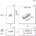
图1是示出根据本公开实施例的存储系统的框图;1 is a block diagram illustrating a storage system according to an embodiment of the present disclosure;
图2是示出图1的存储器控制器的框图;FIG. 2 is a block diagram illustrating the memory controller of FIG. 1;
图3是示出图1的非易失性存储器装置的框图;3 is a block diagram illustrating the nonvolatile memory device of FIG. 1;
图4是示出图3的存储单元阵列的示例的电路图;FIG. 4 is a circuit diagram illustrating an example of the memory cell array of FIG. 3;
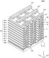
图5是示出与图4的存储块对应的结构的立体图;5 is a perspective view showing a structure corresponding to the memory block of FIG. 4;
图6是示出图5的晶体管结构的剖视图;FIG. 6 is a cross-sectional view showing the structure of the transistor of FIG. 5;
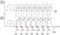
图7是用于描述图4的存储单元的阈值电压分布的示图;FIG. 7 is a diagram for describing a threshold voltage distribution of the memory cell of FIG. 4;
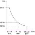
图8是示出读操作中存储单元的误码率的曲线图;8 is a graph showing the bit error rate of a memory cell in a read operation;
图9是示出图1的存储器控制器的操作的流程图;9 is a flowchart illustrating the operation of the memory controller of FIG. 1;
图10至图13是用于描述由图9的非易失性存储器装置执行的刷新读操作的示图;10 to 13 are diagrams for describing a refresh read operation performed by the nonvolatile memory device of FIG. 9;
图14至图16是用于描述由根据本公开实施例的非易失性存储器装置执行的加强刷新读操作的示图;14 to 16 are diagrams for describing an enhanced refresh read operation performed by a nonvolatile memory device according to an embodiment of the present disclosure;
图17和图18是用于描述图14至图16的加强刷新读操作的示图;17 and 18 are diagrams for describing the enhanced refresh read operation of FIGS. 14 to 16;
图19至图22是用于描述由根据本公开实施例的非易失性存储 器装置执行的普通刷新读操作的示图;19 to 22 are diagrams for describing a general refresh read operation performed by a nonvolatile memory device according to an embodiment of the present disclosure;
图23是示出应用了根据本公开实施例的执行刷新读操作的存储系统的固态盘(SSD)系统的示例的框图;23 is a block diagram illustrating an example of a solid state disk (SSD) system to which a storage system performing a refresh read operation according to an embodiment of the present disclosure is applied;
图24是示出应用了根据本公开实施例的执行刷新读操作的存储系统的通用闪速存储(UFS)系统的示例的框图;24 is a block diagram illustrating an example of a Universal Flash Storage (UFS) system to which a memory system performing a refresh read operation according to an embodiment of the present disclosure is applied;
图25是用于描述图24的UFS接口的示图;Figure 25 is a diagram for describing the UFS interface of Figure 24;
图26是用于描述通过SATA接口执行的差分信号传输方法的示图;26 is a diagram for describing a differential signaling method performed through a SATA interface;
图27是用于描述通过SATA接口执行的电源管理方法的示图;27 is a diagram for describing a power management method performed through a SATA interface;
图28是用于描述在省电模式下通过图24的UFS装置执行的加强刷新读操作的示图;以及FIG. 28 is a diagram for describing an enhanced refresh read operation performed by the UFS device of FIG. 24 in a power saving mode; and
图29是用于描述通过图24的UFS系统执行的刷新读操作的示图。FIG. 29 is a diagram for describing a refresh read operation performed by the UFS system of FIG. 24 .
具体实施方式Detailed ways
图1是示出根据本公开实施例的存储系统100的框图。FIG. 1 is a block diagram illustrating a
参照图1,存储系统100可包括存储器控制器110和非易失性存储器装置120。存储系统100还可包括向存储器控制器110和非易失性存储器装置120供应电力的电源模块130。Referring to FIG. 1 , a
存储器控制器110可将数据DATA写入非易失性存储器装置120或者读取存储在非易失性存储器装置120中的数据DATA。非易失性存储器装置120可包括非易失性存储器元件,比如NAND闪速存储器、NOR闪速存储器、相变随机存取存储器(PRAM)、电阻RAM(ReRAM)、磁性RAM(MRAM)等。下面,将基于非易失性存储器装置120包括NAND闪速存储器的假设来描述本公开。例如,假设非易失性存储器装置120包括电荷俘获闪速存储器。The
存储器控制器110可向非易失性存储器装置120发送命令CMD、地址ADDR、控制信号CTRL和数据DATA,从而将数据DATA写入非易失性存储器装置120中。存储器控制器110可向非易失性存储器装置120发送命令CMD、地址ADDR和控制信号CTRL,从而读取存储在非 易失性存储器装置120中的数据DATA。The
非易失性存储器装置120可响应于从存储器控制器110接收的信号执行数据DATA读操作、写操作和擦除操作等。非易失性存储器装置120可包括具有成行(字线)成列(位线)排列的各个存储单元的存储单元阵列122。各存储单元中的每一个可存储1位数据(一位)或M位数据(多位,其中M是等于或大于2的数字)。各存储单元中的每一个可实现为具有电荷存储层(例如浮置栅极或电荷俘获层)的存储单元、具有可变电阻器的存储单元等。The
存储单元阵列122可具有单层阵列结构(2维(2D)阵列结构)或多层阵列结构(3维(3D)阵列结构)。3D存储阵列可在硅衬底上的有源区中以单片方式形成在各存储单元阵列中的至少一个的物理层级(其具有形成在衬底上或衬底中的用于各存储单元的操作的电路)处。术语“单片”表示3D存储阵列每个层级的层直接堆叠在该3D存储阵列的更低层级的层上。The
在根据本公开的技术构思的实施例中,3D存储阵列可包括在竖直方向上布置的NAND串,从而使得至少一个存储单元位于另一存储单元上。所述至少一个存储单元可包括电荷俘获层。以引用方式全文合并于本公开中的美国专利公布第7,679,133号、第8,553,466号、第8,654,587号和第8,559,235号以及美国专利申请公开第2011-0233648号公开了包括多个层级和各层级之间共享的字线和/或位线的3D存储阵列的适当构造。另外,美国专利申请公开第2014-0334232和美国专利公布第8,488,381以引用方式全文合并于本公开中。In an embodiment of the technical concept according to the present disclosure, a 3D memory array may include NAND strings arranged in a vertical direction such that at least one memory cell is located on another memory cell. The at least one memory cell may include a charge trapping layer. US Patent Publication Nos. 7,679,133, 8,553,466, 8,654,587, and 8,559,235, and US Patent Application Publication No. 2011-0233648, which are incorporated by reference in their entirety into this disclosure, disclose the inclusion of multiple tiers and sharing among tiers Proper construction of wordlines and/or bitlines for 3D memory arrays. Additionally, US Patent Application Publication No. 2014-0334232 and US Patent Publication No. 8,488,381 are incorporated by reference into this disclosure in their entirety.
存储器控制器110可包括刷新读控制器111。刷新读控制器111可控制非易失性存储器装置120的存储单元阵列122执行刷新读操作。刷新读操作可防止在对存储单元阵列122的存储单元进行编程后存储单元的电荷随时间损失的现象,并且可维护数据保持。The
刷新读控制器111可控制存储单元阵列122中包括的多个存储块中的每一个执行刷新读操作,该刷新读操作包括针对相应的存储块的多条字线之一的读操作。刷新读控制器111可控制存储块中的每一 个执行一次刷新读操作。The refresh read
电源模块130可执行用于向存储系统100的每个部件供应电力的电源管理。当电源管理集成电路(PMIC)方案应用于电源模块130时,可根据动态电压和频率调整(DVFS)算法实现存储系统100的省电功能。The
电源模块130可检测供应给存储系统100的电力状态。电源模块130可检测电力供应状态中的变化并将电力检测信号PDS发送至存储器控制器110。电源模块130可在存储系统100上电或断电时发送电力检测信号PDS。当存储系统100断电时,电源模块130可根据系统关机命令响应于正常断电或突然断电发送电力检测信号PDS。The
存储器控制器110可响应于电力检测信号PDS控制刷新读控制器111进行操作。刷新读控制器111可响应于电力检测信号PDS同时控制存储单元阵列122的所有存储块连续地执行刷新读操作。刷新读控制器111可响应于电力检测信号PDS控制存储单元阵列122的存储块以刷新读间隔顺序地执行刷新读操作。The
图2是示出图1的存储器控制器110的框图。FIG. 2 is a block diagram illustrating the
参照图2,存储器控制器110可包括刷新读控制器111、中央处理单元(CPU)112、RAM113、ROM114、ECC引擎115、主机接口116和闪存接口117。2 , the
如上文参照图1描述的那样,刷新读控制器111可在存储系统100上电或断电时,控制非易失性存储器装置120中包括的存储单元阵列122的所有存储块同时执行连续地进行刷新读操作的加强刷新读操作。刷新读控制器111可在存储系统100上电后控制存储单元阵列122的存储块执行以刷新读间隔顺序地执行刷新读操作的普通刷新读操作。As described above with reference to FIG. 1 , the refresh read
CPU 112可控制存储器控制器110的主要操作。The
RAM 113可根据CPU 112的控制进行操作,并且可用作存储器控制器110的高速缓存存储器、缓冲存储器、操作存储器等。当RAM 113用作工作存储器时,可临时地存储由CPU112处理的数据。当RAM 113用作缓冲存储器时,可对要从主机HOST发送至图1的非易失性存储 器装置120或要从非易失性存储器装置120发送至主机HOST的数据进行缓冲。当RAM 113用作高速缓存存储器时,非易失性存储器装置120可高速操作。The
ROM 114可将操作存储器控制器110所需的各种类型的信息以固件方式进行存储。例如,CPU 112可读取存储在ROM 114中的固件并驱动所读取的固件。The
例如,刷新读控制器111可实现为固件,可存储在ROM 114或非易失性存储器装置120的一部分中,并且可由CPU 112驱动。可替换地,刷新读控制器111可实现为软件层,可存储在RAM 113中,并且可由CPU 112驱动。For example, flash read
ECC引擎115可检测从非易失性存储器装置120读取的数据的错误并进行纠正。例如,ECC引擎115可通过利用奇偶性纠正错误。ECC引擎115可通过利用诸如低密度奇偶校验(LDPC)码、BCH码、turbo码、卷积码等的编码调制来纠正所读取的数据的错误。The
存储器控制器110可通过主机接口116与主机HOST通信。例如,主机接口116可包括各种接口,例如通用串行总线(USB)、多媒体卡(MMC)、高速外围部件互连(PCI-E)、高级技术附件(ATA)、串行ATA(SATA)、并行ATA(PATA)、串行连接的小型计算机系统(SAS)、小型计算机系统接口(SCSI)、嵌入式MMC(eMMC)和增强型小型磁盘接口(ESDI)等。The
存储器控制器110可通过闪存接口117与非易失性存储器装置120通信。例如,闪存接口117可配置为支持NAND闪速存储器、多电平闪速存储器和单电平闪速存储器。
图3是示出图1的非易失性存储器装置120的框图。FIG. 3 is a block diagram illustrating the
参照图3,非易失性存储器装置120可包括存储单元阵列122、地址解码器123、控制逻辑124和输入/输出(I/O)电路125。3 , the
存储单元阵列122可连接至字线WL、串选择线SSL、地选择线GSL和位线BL。存储单元阵列122可以通过字线WL、串选择线SSL和地选择线GSL连接至地址解码器123,并且通过位线BL连接至I/O电路125。存储单元阵列122可包括多个存储块BLK1至BLKn。The
每个存储块BLK1至BLKn可包括多个存储单元和多个选择晶体管。存储单元可连接至字线WL。选择晶体管可连接至串选择线SSL或地选择线GSL。存储块BLK1至BLKn中的每一个的存储单元可形成为存储1位数据的单电平单元或形成为存储多位数据的多电平单元。存储块BLK1至BLKn中的每一个的存储单元可通过在垂直于衬底的方向上堆叠而形成3D结构。将参照图4和图5详细描述存储块的结构。Each of the memory blocks BLK1 to BLKn may include a plurality of memory cells and a plurality of selection transistors. Memory cells may be connected to word lines WL. The selection transistors may be connected to either the string selection line SSL or the ground selection line GSL. The memory cells of each of the memory blocks BLK1 to BLKn may be formed as single-level cells storing 1-bit data or as multi-level cells storing multiple-bit data. The memory cells of each of the memory blocks BLK1 to BLKn may form a 3D structure by being stacked in a direction perpendicular to the substrate. The structure of the memory block will be described in detail with reference to FIGS. 4 and 5 .
地址解码器123可对存储单元阵列122的字线WL执行选择操作和驱动操作。地址解码器123可从存储控制器110接收地址ADDR,可对接收到的地址ADDR进行解码,并且可驱动多条字线WL。The
控制逻辑124可从存储控制器110接收命令CMD和控制信号CTRL,并且可以响应于接收到的信号来控制地址解码器123和I/O电路125。例如,控制逻辑124可响应于命令CMD和控制信号CTRL而控制地址解码器123和I/O电路125将数据DATA写入存储单元阵列122。控制逻辑124可响应于命令CMD和控制信号CTRL而控制地址解码器123和I/O电路125输出存储在存储单元阵列122中的数据DATA。控制逻辑124可响应于命令CMD和控制信号CTRL而控制地址解码器123和I/O电路125擦除存储单元阵列122的一部分。
控制逻辑124可控制电压生成器,其生成操作非易失性存储器件120所需的各种电压。例如,电压生成器可生成各种电压,例如多个选择读取电压、多个非选择读取电压、多个编程电压、多个导通电压和多个擦除电压,并且向地址解码器122提供所生成的电压。
I/O电路125可通过多条位线BL连接至存储单元阵列122。I/O电路125可控制多条位线BL,使得将从存储控制器110接收的数据DATA写入存储单元阵列122。I/O电路125可控制多条位线BL以输出存储在存储单元阵列122中的数据DATA。The I/
I/O电路125可包括页缓冲器126。例如,I/O电路125可包括诸如列选择电路、写驱动器、检测放大器、数据缓冲器等的部件。在读操作期间,页缓冲器126可连接至从存储块BLK1至BLKn中读取的存储单元的位线BL。页缓冲器126可对位线BL的电压电平与预定的参考电压进行比较,并将取决于比较结果的逻辑值存储在连接至相应 位线BL的锁存器中。I/
在存储块BLK1至BLKn的刷新读操作期间,页缓冲器126可连接至相应的存储块的位线BL,可对所连接的位线BL的电压电平与预定的参考电压进行比较,并且将比较结果存储在锁存器中。根据实施例,虽然页缓冲器126在刷新读操作期间连接至相应的存储块的位线BL,但是页缓冲器126可无视或者可不执行对所连接的位线BL的电压电平与预定的参考电压进行比较以及存储比较结果的操作。根据另一实施例,在刷新读操作期间,页缓冲器126可不连接至相应的存储块的位线BL。During a refresh read operation of the memory blocks BLK1 to BLKn, the
图4是示出图3的存储单元阵列122的示例的电路图。对参照图3描述的存储块BLK1至BLKn中的第一存储块BLK1的一部分进行描述,但是本公开不限于此。其它存储块BLK2至BLKn可具有与第一存储块BLK1相同的结构。FIG. 4 is a circuit diagram illustrating an example of the
第一存储块BLK1可包括多个NAND串NS11至NS22、多条字线WL1至WL8、多条位线BL1和BL2、地选择线GSL、串选择线SSL和公共源极线CSL。串选择线SSL可划分为第一串选择线SSL1和第二串选择线SSL2。就这一点而言,可根据实施例不同地改变NAND串的数量、字线的数量、位线的数量、地选择线的数量和串选择线的数量。The first memory block BLK1 may include a plurality of NAND strings NS11 to NS22, a plurality of word lines WL1 to WL8, a plurality of bit lines BL1 and BL2, a ground selection line GSL, a string selection line SSL, and a common source line CSL. The string selection line SSL can be divided into a first string selection line SSL1 and a second string selection line SSL2. In this regard, the number of NAND strings, the number of word lines, the number of bit lines, the number of ground select lines, and the number of string select lines may vary variously according to the embodiment.
第一存储块BLK1可构造为利用划分的串选择线SSL1和SSL2的奇偶架构。位线BL1和BL2可分成偶数位线BL1e和BL2e以及奇数位线BL1o和BL2o。在奇偶架构中,包括在公共字线中并连接至奇数位线BL1o和BL2o的存储单元可在第一时间编程或读取,而包括在公共字线中并连接至偶数位线BL1e和BL2e的存储单元可在第二时间编程或读取。The first memory block BLK1 may be constructed in a parity architecture using divided string selection lines SSL1 and SSL2. The bit lines BL1 and BL2 may be divided into even-numbered bit lines BL1e and BL2e and odd-numbered bit lines BL1o and BL2o. In an odd-even architecture, memory cells included in a common word line and connected to odd bit lines BL1o and BL2o can be programmed or read at a first time, while memory cells included in a common word line and connected to even bit lines BL1e and BL2e The memory cells can be programmed or read at the second time.
在实施例中,第一存储块BLK1可构造为利用一条串选择线SSL的全位线(ABL)架构。在ABL架构中,所有位线BL1和BL2可同时选择读操作和编程操作。包括在公共字线中并连接至所有位线BL1和BL2的存储单元可同时编程或读取。In an embodiment, the first memory block BLK1 may be configured as an all bit line (ABL) architecture using one string select line SSL. In the ABL architecture, all bit lines BL1 and BL2 can simultaneously select read and program operations. Memory cells included in a common word line and connected to all bit lines BL1 and BL2 can be programmed or read simultaneously.
NAND串NS11和NS21可设置在第一位线BL1和公共源极线CSL之间。NAND串NS12和NS22可设置在第二位线BL2和公共源极线CSL 之间。每个NAND串(例如,NS11)可包括串联连接的串选择晶体管SST、多个存储单元MC1至MC8和地选择晶体管GST。The NAND strings NS11 and NS21 may be disposed between the first bit line BL1 and the common source line CSL. NAND strings NS12 and NS22 may be disposed between the second bit line BL2 and the common source line CSL. Each NAND string (eg, NS11 ) may include a series-connected string selection transistor SST, a plurality of memory cells MC1 to MC8 , and a ground selection transistor GST.
共同连接至单条位线的NAND串可构成单列。例如,共同连接至第一位线BL1的NAND串NS11和NS21可对应于第一列,并且共同连接至第二位线BL2的NAND串NS12和NS22可对应于第二列。NAND strings that are commonly connected to a single bit line can form a single column. For example, the NAND strings NS11 and NS21 commonly connected to the first bit line BL1 may correspond to the first column, and the NAND strings NS12 and NS22 commonly connected to the second bit line BL2 may correspond to the second column.
共同连接至单条串选择线的NAND串可构成单行。例如,共同连接至第一串选择线SSL1的NAND串NS11和NS12可对应于第一行,并且共同连接至第二串选择线SSL2的NAND串NS21和NS22可对应于第二行。NAND strings connected together to a single string select line can form a single row. For example, the NAND strings NS11 and NS12 commonly connected to the first string selection line SSL1 may correspond to the first row, and the NAND strings NS21 and NS22 commonly connected to the second string selection line SSL2 may correspond to the second row.
串选择晶体管SST可连接至相应的串选择线SSL1和SSL2。多个存储单元MC1至MC8可分别连接至相应的字线WL1至WL8。地选择晶体管GST可连接至相应的地选择线GSL。串选择晶体管SST可连接至相应的位线BL1和BL2。地选择晶体管GST可连接至公共源极线CSL。The string selection transistors SST may be connected to corresponding string selection lines SSL1 and SSL2. The plurality of memory cells MC1 to MC8 may be connected to corresponding word lines WL1 to WL8, respectively. The ground selection transistors GST may be connected to corresponding ground selection lines GSL. String selection transistors SST may be connected to corresponding bit lines BL1 and BL2. The ground selection transistor GST may be connected to the common source line CSL.
在本实施例中,具有相同高度的字线(例如WL1)可彼此共同连接。例如,当对连接至第一字线WL1并包括在NAND串NS11和NS12中的存储单元进行编程时,可选择第一字线WL1和第一串选择线SSL1。In this embodiment, word lines (eg, WL1 ) having the same height may be commonly connected to each other. For example, when programming memory cells connected to the first word line WL1 and included in the NAND strings NS11 and NS12, the first word line WL1 and the first string selection line SSL1 may be selected.
NAND串的列数可增加或减少。随着NAND串的列数改变,连接至NAND串的列的位线的数量和连接至一条串选择线的NAND串的数量也可改变。The number of columns of NAND strings can be increased or decreased. As the number of columns of NAND strings changes, the number of bit lines connected to a column of NAND strings and the number of NAND strings connected to a string select line may also change.
NAND串的高度可增加或减小。例如,堆叠在每个NAND串上的存储单元的数量可增加或减少。随着堆叠在每个NAND串上的存储单元的数量改变,字线的数量也可改变。例如,提供给每个NAND串的串选择晶体管或地选择晶体管的数量可增加。随着提供给每个NAND串的串选择晶体管或地选择晶体管的数量改变,串选择线或地选择线的数量也可改变。如果串选择晶体管或地选择晶体管的数量增加,则串选择晶体管或地选择晶体管可以按存储单元MC1至MC8的形式堆叠。The height of the NAND strings can be increased or decreased. For example, the number of memory cells stacked on each NAND string can be increased or decreased. As the number of memory cells stacked on each NAND string changes, the number of word lines can also change. For example, the number of string select transistors or ground select transistors provided to each NAND string may be increased. As the number of string select transistors or ground select transistors provided to each NAND string changes, so can the number of string select lines or ground select lines. If the number of the string selection transistors or the ground selection transistors is increased, the string selection transistors or the ground selection transistors may be stacked in the form of memory cells MC1 to MC8 .
例如,可以以NAND串NS11、NS12、NS21和NS22的行为单位来执行编程操作和读操作。可通过串选择线SSL1和SSL2以单个行为单位选择NAND串NS11、NS12、NS21和NS22。可通过第一串选择线SSL1以单个行为单位选择NAND串NS11和NS12。可通过第二串选择线SSL2以单个行为单位选择NAND串NS21和NS22。For example, a program operation and a read operation may be performed in units of rows of NAND strings NS11, NS12, NS21, and NS22. The NAND strings NS11, NS12, NS21 and NS22 can be selected in a single row unit through the string selection lines SSL1 and SSL2. The NAND strings NS11 and NS12 can be selected in a single row unit through the first string selection line SSL1. The NAND strings NS21 and NS22 can be selected in a single row unit through the second string selection line SSL2.
可在所选择的各行NAND串NS11、NS12、NS21和NS22中以页为单位执行编程操作和读操作。页可以是连接至单条字线的单行存储单元。可通过字线WL1至WL8在所选择的各行NAND串NS11、NS12、NS21和NS22中以页为单位选择存储单元。Program operations and read operations may be performed in units of pages in the selected rows of NAND strings NS11, NS12, NS21, and NS22. A page may be a single row of memory cells connected to a single word line. Memory cells can be selected in units of pages in the selected rows of NAND strings NS11, NS12, NS21, and NS22 through word lines WL1 to WL8.
图5是示出对应于图4的存储块BLK1的结构的立体图。FIG. 5 is a perspective view showing the structure of the memory block BLK1 corresponding to FIG. 4 .
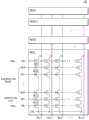
参照图5,存储块BLK1可形成在垂直于衬底SUB的方向上。在图5中,虽然将存储块BLK1示出为包括两条选择线GSL和SSL、八条字线WL1至WL8和三条位线BL1至BL3,但是存储块BLK1实际上可包括更多的线或更少的线。Referring to FIG. 5, the memory blocks BLK1 may be formed in a direction perpendicular to the substrate SUB. In FIG. 5, although the memory block BLK1 is shown as including two select lines GSL and SSL, eight word lines WL1 to WL8, and three bit lines BL1 to BL3, the memory block BLK1 may actually include more lines or more less lines.
可在具有第一导电类型(例如,p型)的衬底SUB上提供沿着第一方向(例如,Y方向)延伸并掺杂有具有第二导电类型(例如,n型)的杂质的公共源极线CSL。沿着第一方向延伸的多个绝缘层IL可沿着第三方向(例如,Z方向)顺序地设置在衬底SUB的位于两条相邻的公共源极线CSL之间的区域上,并且可沿着第三方向彼此间隔开预定距离。例如,多个绝缘层IL可包括诸如氧化硅的绝缘材料。A common extending along a first direction (eg, Y direction) and doped with impurities having a second conductivity type (eg, n-type) may be provided on the substrate SUB having a first conductivity type (eg, p-type) source line CSL. A plurality of insulating layers IL extending along the first direction may be sequentially disposed along a third direction (eg, the Z direction) on a region of the substrate SUB located between two adjacent common source lines CSL, and They may be spaced apart from each other by a predetermined distance along the third direction. For example, the plurality of insulating layers IL may include insulating materials such as silicon oxide.
沿着第一方向顺序设置并在第三方向上穿过多个绝缘层IL的多个柱P可设置在衬底SUB的位于两条相邻的公共源极线CSL之间的区域上。例如,多个柱P可穿过多个绝缘层IL以与衬底SUB接触。更具体地,每个柱P的表面层S可包括具有p型的硅材料并且用作沟道区。同时,每个柱P的内层I可包括诸如氧化硅的绝缘材料或气隙。A plurality of pillars P sequentially disposed along the first direction and passing through the plurality of insulating layers IL in the third direction may be disposed on a region of the substrate SUB between two adjacent common source lines CSL. For example, a plurality of pillars P may pass through a plurality of insulating layers IL to be in contact with the substrate SUB. More specifically, the surface layer S of each pillar P may include a silicon material having a p-type and serve as a channel region. Meanwhile, the inner layer I of each pillar P may include an insulating material such as silicon oxide or an air gap.
在两条相邻的公共源极线CSL之间的区域中,可沿着绝缘层IL、柱P和衬底SUB的暴露表面设置电荷存储层CS。电荷存储层CS可包括栅极绝缘层(其也可称作“隧道绝缘层”)、电荷俘获层和阻挡绝缘层。例如,电荷存储层CS可具有氧化物-氮化物-氧化物(ONO)结构。在两条相邻的公共源极线CSL之间的区域中,可在电荷存储层CS的暴露表面上设置诸如选择线GSL和SSL以及字线WL1至WL8之类的栅电极GE。In a region between two adjacent common source lines CSL, a charge storage layer CS may be disposed along the insulating layer IL, the pillar P, and the exposed surface of the substrate SUB. The charge storage layer CS may include a gate insulating layer (which may also be referred to as a 'tunnel insulating layer'), a charge trapping layer, and a blocking insulating layer. For example, the charge storage layer CS may have an oxide-nitride-oxide (ONO) structure. In a region between two adjacent common source lines CSL, gate electrodes GE such as select lines GSL and SSL and word lines WL1 to WL8 may be disposed on the exposed surface of the charge storage layer CS.
漏极或漏极接触件DR可分别设置在多个柱P上。例如,漏极或漏极接触件DR可包括掺杂有具有第二导电类型的杂质的硅材料。可 在漏极接触件DR上设置在第二方向(例如,X方向)上延伸且沿第一方向彼此间隔开预定距离的位线BL1至BL3。The drain or drain contacts DR may be disposed on the plurality of pillars P, respectively. For example, the drain or drain contact DR may include a silicon material doped with impurities having the second conductivity type. Bit lines BL1 to BL3 extending in the second direction (eg, the X direction) and spaced apart from each other along the first direction by a predetermined distance may be disposed on the drain contact DR.
柱P中的每一个可与绝缘层IL和在第三方向上排列的选择线GSL和SSL以及字线WL1至WL8一起形成NAND串NS。NAND串NS可包括多个晶体管结构TS。将参照图6详细描述晶体管结构TS。Each of the pillars P may form a NAND string NS together with the insulating layer IL and the select lines GSL and SSL and the word lines WL1 to WL8 arranged in the third direction. A NAND string NS may include a plurality of transistor structures TS. The transistor structure TS will be described in detail with reference to FIG. 6 .
图6是示出图5的晶体管结构TS的剖视图。FIG. 6 is a cross-sectional view showing the transistor structure TS of FIG. 5 .
参照图6,柱P的表面层S可为p型硅并且将用作主体。电荷存储层CS可包括隧道绝缘层17、电荷俘获层18和阻挡绝缘层19。与柱P相邻的隧道绝缘层17可包括氧化硅层。电荷俘获层18可包括氮化硅层。阻挡绝缘层19可包括具有高介电常数的高介电层或金属氧化物层(例如,氧化铝层和氧化铪层)。下面将柱P的p型硅S称作主体。Referring to FIG. 6 , the surface layer S of the pillar P may be p-type silicon and will serve as a host. The charge storage layer CS may include a
由于栅电极GE和主体S之间的电压差,会在栅电极GE和主体S之间形成电场。电场可分布至隧道绝缘层17、电荷俘获层18和阻挡绝缘层19。Due to the voltage difference between the gate electrode GE and the body S, an electric field is formed between the gate electrode GE and the body S. The electric field may be distributed to the
分布至隧道绝缘层17的电场可导致Fowler-Nordheim隧穿。存储单元MC可通过分布至隧道绝缘层17的电场来编程或擦除。也就是说,可通过分布至隧道绝缘层17的电场来确定在编程操作期间由电荷俘获层18俘获的电荷的量或在擦除操作期间从电荷俘获层18流出的电荷的量。存储单元MC可构造为电荷俘获闪速(CTF)存储单元。The electric field distributed to the
存储在电荷存储层CS中的电荷可在CTF存储单元编程之后随时间放电。随着重复编程和擦除操作的次数增加,隧道绝缘层17劣化,因此,在CTF存储单元中电荷损失现象可能变得更严重。因此,存储单元MC的阈值电压可能改变。下面将参照图7描述存储单元MC的阈值电压变化。The charge stored in the charge storage layer CS may be discharged over time after programming of the CTF memory cell. As the number of repeated program and erase operations increases, the
图7是用于描述图4的存储单元的阈值电压分布的示图。为了使描述简洁,假设存储单元是三电平单元(TLC)。本公开不限于此。各存储单元中的每一个可设置为存储单个位的单电平单元(SLC)或者存储至少两个位的多电平单元(MLC)。可替换地,可将各存储单元中的每一个的操作模式可变地改变为SLC模式或MLC模式。FIG. 7 is a diagram for describing a threshold voltage distribution of the memory cell of FIG. 4 . For the sake of brevity of description, it is assumed that the memory cell is a three-level cell (TLC). The present disclosure is not limited thereto. Each of the memory cells may be configured as a single-level cell (SLC) storing a single bit or a multi-level cell (MLC) storing at least two bits. Alternatively, the operation mode of each of the memory cells may be variably changed to the SLC mode or the MLC mode.
参照图7,存储单元可编程为处于擦除状态E和第一编程状态P1至第七编程状态P7中的一个。例如,可基于第一验证电压VP1至第七验证电压VP7将存储单元编程为处于擦除状态E和第一编程状态P1至第七编程状态P7中的一个。Referring to FIG. 7, a memory cell can be programmed to be in an erased state E and one of a first programming state P1 to a seventh programming state P7. For example, the memory cells may be programmed to be in one of the erased state E and the first to seventh program states P1 to P7 based on the first to seventh verification voltages VP1 to VP7.
存储单元的阈值电压可能会在存储单元编程之后随时间改变。例如,在存储单元编程之后,编程为处于第七编程状态P7的存储单元可能随时间成为编程状态P7'。也就是说,编程为处于第七编程状态P7的存储单元可能具有高于第七验证电压VP7的阈值电压。编程为处于第七编程状态P7的存储单元的阈值电压可能小于第七验证电压VP7,使得编程为必须处于第七编程状态P7的存储单元在该存储单元编程之后可能随时间处于编程状态P7'。The threshold voltage of a memory cell may change over time after the memory cell is programmed. For example, memory cells programmed to be in the seventh programming state P7 may become programmed state P7' over time after programming of the memory cells. That is, memory cells programmed to be in the seventh program state P7 may have a threshold voltage higher than the seventh verification voltage VP7. The threshold voltages of memory cells programmed to be in the seventh programming state P7 may be less than the seventh verify voltage VP7, so that memory cells programmed to necessarily be in the seventh programming state P7 may be in the programmed state P7' over time after the memory cells are programmed.
同样,编程为处于第一编程状态P1至第六编程状态P6中的存储单元在该存储单元编程之后可能随时间分别处于编程状态P1'至P6'。这可理解为表示存储在存储单元的电荷存储层中的电荷随时间移动到沟道层,从而使得存储单元的阈值电压减小。存储单元的阈值电压分布可称作电荷损失现象。Likewise, memory cells programmed to be in the first programming state P1 to the sixth programming state P6 may be in programming states P1 ′ to P6 ′, respectively, over time after the memory cell is programmed. This can be understood to mean that the charges stored in the charge storage layer of the memory cell move to the channel layer over time, thereby reducing the threshold voltage of the memory cell. The threshold voltage distribution of a memory cell may be referred to as a charge loss phenomenon.
当基于具有变化的阈值电压的存储单元来读取数据时,所读取的数据可能包括错误。例如,存储单元可基于第一选择读取电压Vrd1至第七选择读取电压Vrd7识别其编程状态。第一选择读取电压Vrd1至第七选择读取电压Vrd7可具有用于识别第一编程状态P1至第七编程状态P7的电压电平。在经过预定时间段之后,存储单元可能具有取决于电荷丢失现象的编程状态P1'至P7'。就这一点而言,当基于第一选择读取电压Vrd1至第七选择读取电压Vrd7执行读操作时,所读取的数据可能包括错误。When reading data based on memory cells having varying threshold voltages, the read data may include errors. For example, a memory cell may identify its program state based on the first to seventh selection read voltages Vrd1 to Vrd7. The first to seventh selection read voltages Vrd1 to Vrd7 may have voltage levels for identifying the first to seventh program states P1 to P7. After a predetermined period of time, the memory cells may have programmed states P1' to P7' depending on the charge loss phenomenon. In this regard, when a read operation is performed based on the first to seventh selection read voltages Vrd1 to Vrd7, the read data may include errors.
图8是示出读操作中存储单元的误码率的曲线图。FIG. 8 is a graph showing a bit error rate of a memory cell in a read operation.
参照图8,当非易失性存储器装置120执行读操作时,包括在第一读操作期间读取的数据中的误码率BER1会很高。较高的误码率BER1可能无法使用图2的ECC引擎115来校正。8, when the
第一读操作可能会在存储单元编程之后执行。因此,在存储单元编程之后直到执行第一读操作,误码率会随着更多时间的流逝而增 加。这可理解为表示存储单元处于图7的编程状态P1'至P7'的概率增加,编程状态P1'至P7'具有由于存储单元随时间丢失电荷的现象而改变的阈值电压。The first read operation may be performed after the memory cell is programmed. Therefore, the bit error rate increases over more time after the memory cell is programmed until the first read operation is performed. This can be understood as representing an increased probability of memory cells being in programmed states P1 ′ to P7 ′ of FIG. 7 , which have threshold voltages that vary due to the phenomenon of memory cells losing charge over time.
在第二读操作期间的误码率BER2会远小于在第一读操作期间的误码率BER1。在第三读操作期间的误码率BER3会小于在第二读操作期间的误码率BER2。The bit error rate BER2 during the second read operation will be much smaller than the bit error rate BER1 during the first read operation. The bit error rate BER3 during the third read operation will be smaller than the bit error rate BER2 during the second read operation.
来自于第二读操作的误码率BER2减小的原因很可能是因为通过第一读操作使得存储单元的电荷损失得到了一定程度的补偿。也就是说,在第一读操作期间电压施加到图3的存储单元阵列122,从而可补偿存储单元的阈值电压变化。例如,由于在第一读操作期间施加到选择线CSL和SSL以及字线WL1到WL8的电压,导致移动到沟道层的电荷可以(但不是全部地)移动到电荷存储层,因此存储单元的阈值电压可增加。这种通过读操作来补偿电荷损失的操作称作刷新读操作。The reason for the decrease in the bit error rate BER2 from the second read operation is probably because the charge loss of the memory cells is compensated to some extent by the first read operation. That is, a voltage is applied to the
为了防止由于非易失性存储器件120的已编程的存储单元的电荷损失而发生错误,非易失性存储器装置120可设计为执行刷新读操作。然而,由于在非易失性存储器装置120执行编程操作之后需要多长时间来执行读操作是未知的,因此难以执行最优的刷新读操作。To prevent errors from occurring due to loss of charge in programmed memory cells of the
根据本公开的各实施例,存储器控制器110可在存储系统100通电时控制非易失性存储器装置120的刷新读操作。存储器控制器110可在存储系统100断电时控制非易失性存储器装置120的刷新读操作。存储器控制器110可在驱动存储系统100时周期性地控制非易失性存储器装置120的刷新读操作。According to various embodiments of the present disclosure, the
图9是示出图1的存储器控制器110的操作的流程图。FIG. 9 is a flowchart illustrating the operation of the
存储器控制器110可检测存储系统100的上电或断电。例如,存储器控制器110可接收从电源模块130提供的电力检测信号PDS以检测存储系统100的上电或断电。根据系统关机命令,存储系统100的断电可包括可预见的正常断电或不可预见的突然断电。The
例如,可通过检测非易失性存储器装置120的上电或断电来提供电源模块130的电力检测信号PDS。因此,存储器控制器110可检测非易失性存储器装置120的上电或断电。For example, the power detection signal PDS of the
在操作S920中,存储器控制器110可在存储系统100或非易失性存储器装置120上电或断电时发出刷新读命令RRD CMD。例如,存储器控制器110可响应于电源模块130的电力检测信号PDS发出刷新读命令RRD CMD,并将刷新读命令RRD CMD提供给非易失性存储器装置120。刷新读命令RRD CMD可指示图3的包括在非易失性存储器装置120的存储单元阵列122中的所有存储块BLK1至BLKn同时执行连续地进行刷新读操作的加强刷新读操作。In operation S920, the
例如,当存储系统100上电之后驱动存储器控制器110时,存储器控制器110可发出刷新读命令RRD CMD。刷新读命令RRD CMD可指示包括在非易失性存储器装置120的存储单元阵列122中的图3的所有存储块BLK1至BLKn执行以刷新读间隔顺序地进行刷新读操作的普通刷新读操作。For example, when the
在操作S930中,存储器控制器110可控制接收刷新读命令RRD CMD的非易失性存储器装置120执行刷新读操作。例如,非易失性存储器装置120可执行加强刷新读操作或普通刷新读操作。In operation S930, the
存储单元阵列122的所有存储块BLK1至BLKn可根据加强刷读操作同时连续地执行刷新读操作,从而补偿由于存储块BLK1至BLKn的存储单元的电荷损失而导致的数据劣化。所有存储块BLK1至BLKn可根据正常刷新读操作而在刷新读间隔期间顺序地执行刷新读操作,从而维护存储块BLK1至BLKn的存储单元的数据保持。All the memory blocks BLK1 to BLKn of the
就这一点而言,可执行刷新读操作以防止非易失性存储器装置120的数据劣化并且维护数据保持,因此用于识别所读取的存储单元数据的存储块BLK1至BLKn的位线BL的电压电平不重要。因此,存储块BLK1至BLKn的位线BL可不连接至图3的I/O电路125的页缓冲器126。In this regard, a refresh read operation may be performed to prevent data degradation of the
根据实施例,尽管存储块BLK1至BLKn的位线BL连接至页缓冲器126,但是对位线BL的电压电平和预定参考电压进行比较并存储比较结果的操作可不予处理,或者可不由页缓冲器126执行。According to an embodiment, although the bit lines BL of the memory blocks BLK1 to BLKn are connected to the
随后,可不将非易失性存储器装置120执行的刷新读操作的结果提供给存储器控制器110。Subsequently, the results of the refresh read operation performed by the
图10至图13是用于描述由图9的非易失性存储器装置120执行的刷新读操作的示图。10 to 13 are diagrams for describing a refresh read operation performed by the
参照图1、图9和图10,在操作S920中,存储器控制器110可发出刷新读命令RRDCMD,并向非易失性存储器装置120提供刷新读命令RRD CMD。在操作S1010中,非易失性存储器装置120可响应于刷新读命令RRD CMD从包括在存储单元阵列122中的存储块BLK1至BLKn中的每一个选择单个页(或单条字线)。1 , 9 and 10 , in operation S920 , the
例如,根据由存储器控制器110提供的地址ADDR,可从存储块BLK1至BLKn中的每一个选择相同的页或不同的页。根据实施例,当存储块BLK1至BLKn划分为预定组时,从第一组中选择的页可不同于从第二组中选择的页。For example, the same page or a different page may be selected from each of the memory blocks BLK1 to BLKn according to the address ADDR provided by the
在操作S1020中,非易失性存储器装置120可对从存储块BLK1至BLKn中的每一个中选择的页执行读操作。例如,对所选择的页的读操作可向所选择的页施加选择读取电压,并且读取连接至所选择的页的存储单元的数据。In operation S1020, the
就这一点而言,一般的读操作可确定存储单元的阈值电压分布是低于选择读取电压还是高于选择读取电压从而读取存储单元数据,因此重要的是选择所述选择读取电压。然而,刷新读操作将选择读取电压施加到所选择的字线是为了防止存储单元的数据劣化并维护数据保持,因此选择所述选择读取电压并不重要。因此,在刷新读操作期间施加到选择的字线的选择读取电压可设置为图7的多个选择读取电压Vrd1至Vrd7中的任一个。In this regard, a typical read operation can determine whether the threshold voltage distribution of the memory cell is below or above the select read voltage to read the memory cell data, so it is important to select the select read voltage . However, the refresh read operation applies the select read voltage to the selected word line in order to prevent data degradation of the memory cells and maintain data retention, so the selection of the select read voltage is not critical. Therefore, the select read voltage applied to the selected word line during the refresh read operation may be set to any one of the plurality of select read voltages Vrd1 to Vrd7 of FIG. 7 .
参照图11,示出了在刷新读操作期间将电压施加到存储单元阵列122的实施例。例如,可通过包括在非易失性存储器装置120的存储单元阵列122中的存储块BLK1至BLKn当中的第一存储块BLK1来执行刷新读操作。对第一存储块BLK1的刷新读操作描述为对从多条字线WL1至WL8中选择的单条字线WL1执行的读操作。Referring to FIG. 11, an embodiment is shown in which a voltage is applied to the
可将串选择电压VSSL施加到串选择线SSL,并且可将地选择电压VGSL施加到地选择线GSL,从而使得在第一存储块BLK1中串选择晶体管SST和地选择晶体管GST导通。例如,串选择电压VSSL和地 选择电压VGSL可以是读取电压Vread、电源电压VDD或具有与其类似的电平的电压。The string selection voltage VSSL may be applied to the string selection line SSL, and the ground selection voltage VGSL may be applied to the ground selection line GSL, thereby turning on the string selection transistor SST and the ground selection transistor GST in the first memory block BLK1. For example, the string selection voltage VSSL and the ground selection voltage VGSL may be the read voltage Vread, the power supply voltage VDD, or a voltage having a level similar thereto.
可将读取电压Vread施加到未选择的字线WL2到WL8,并且可将第一选择读取电压Vrd1施加到第一存储块BLK1中的所选择的字线WL1。读取电压Vread可具有比存储单元的阈值电压Vth的分布电平更高的电平,如图7所示。因此,施加了读取电压Vread的所有存储单元MC2至MC8可导通。第一选择读取电压Vrd1可设置为具有用于确定第一编程状态P1至第七编程状态P7的电压Vrd1至Vrd7中的最低电压电平,如图7所示。The read voltage Vread may be applied to the unselected word lines WL2 to WL8, and the first selected read voltage Vrd1 may be applied to the selected word line WL1 in the first memory block BLK1. The read voltage Vread may have a higher level than the distribution level of the threshold voltage Vth of the memory cell, as shown in FIG. 7 . Therefore, all the memory cells MC2 to MC8 to which the read voltage Vread is applied can be turned on. The first selection read voltage Vrd1 may be set to have the lowest voltage level among the voltages Vrd1 to Vrd7 for determining the first to seventh program states P1 to P7 , as shown in FIG. 7 .
例如,在第一存储块BLK1中,位线BL1至BLm可预充电至电源电压VDD。For example, in the first memory block BLK1, the bit lines BL1 to BLm may be precharged to the power supply voltage VDD.
位线BL1至BLm的电压电平可根据连接至所选择的字线WL1的存储单元的数据而改变。例如,如果在连接至所选择的字线WL1的存储单元中存在具有低于第一选择读取电压Vrd1的阈值电压的存储单元,则预充电至相应位线BL的电源电压VDD可放电到公共源极线CSL,从而可减小位线BL的电压。如果在连接至所选择的字线WL1的存储单元中存在具有高于第一选择读取电压Vrd1的阈值电压的存储单元,则相应的位线BL可保持预充电的电源电压VDD的电平。The voltage levels of the bit lines BL1 to BLm may vary according to data of memory cells connected to the selected word line WL1. For example, if a memory cell having a threshold voltage lower than the first selection read voltage Vrd1 exists among the memory cells connected to the selected word line WL1, the power supply voltage VDD precharged to the corresponding bit line BL may be discharged to the common source line CSL, thereby reducing the voltage of the bit line BL. If a memory cell having a threshold voltage higher than the first selection read voltage Vrd1 exists among the memory cells connected to the selected word line WL1, the corresponding bit line BL may maintain the level of the precharged power supply voltage VDD.
位线BL1至BLm可连接至图3的I/O电路125的页缓冲器126。当位线BL1至BLm的电压电平低于预定电压电平时,页缓冲器126可在与相应的位线BL连接的锁存器中存储例如逻辑低。当位线BL1至BLm的电压电平高于预定电压电平时,页缓冲器126可在与相应的位线BL连接的锁存器中存储例如逻辑高。The bit lines BL1 to BLm may be connected to the
根据实施例,位线BL可不连接至图3的I/O电路125的页缓冲器126。这种情况下,可通过仅向串选择线SSL、地选择线GSL、未选择的字线WL2至WL8和选择的字线WL1施加电压电平来执行刷新读操作。According to an embodiment, the bit line BL may not be connected to the
根据实施例,第一存储块BLK1的刷新读操作可替换为针对多条字线WL1至WL8中的字线WL2至WL8之一的读操作,而不是针对第一字线WL1的读操作。例如,可基于将第二字线WL2设置为所选择的字 线并且将其它字线WL1和WL3至WL8设置为未选择的字线的读操作来执行第一存储块BLK1的刷新读操作。According to an embodiment, the refresh read operation of the first memory block BLK1 may be replaced with a read operation for one of the word lines WL2 to WL8 among the plurality of word lines WL1 to WL8 instead of the read operation for the first word line WL1 . For example, the refresh read operation of the first memory block BLK1 may be performed based on a read operation of setting the second word line WL2 as the selected word line and setting the other word lines WL1 and WL3 to WL8 as unselected word lines.
根据实施例,第一存储块BLK1的刷新读操作可选择选择读取电压Vrd2至Vrd7中的一个,而不是第一选择读取电压Vrd1,并将所选择的选择读取电压施加到所选择的字线WL1。例如,可通过将第二选择读取电压Vrd2施加到所选择的字线WL1来执行第一存储块BLK1的刷新读操作。According to an embodiment, the refresh read operation of the first memory block BLK1 may select one of the selection read voltages Vrd2 to Vrd7 instead of the first selection read voltage Vrd1 and apply the selected selection read voltage to the selected word line WL1. For example, the refresh read operation of the first memory block BLK1 may be performed by applying the second selection read voltage Vrd2 to the selected word line WL1.
同样地,存储器控制器110可通过从包括在相应的存储块BLK2至BLKn中的多条字线WL1至WL8中选择第一字线WL1、将第一选择读取电压Vrd1施加到所选择的字线WL1以及将读取电压Vread施加到未选择的字线WL2到WL8,来执行存储块BLK1至BLKn中的除第一存储块BLK1之外的每一个的刷新读操作。相应的存储块BLK2至BLKn的位线BL1至BLm可预充电到电源电压VDD,并且可具有根据连接至所选择的字线WL1的存储单元的数据而改变的电压电平。对应的存储块BLK2至BLKn的位线BL1至BLm的电压电平可提供给图3的I/O电路125的页缓冲器126。根据一个实施例,对应的存储块BLK2至BLKn的位线BL1至BLm的电压电平可不提供给图3的I/O电路125的页缓冲器126。Likewise, the
根据实施例,存储块BLK2至BLKn的刷新读操作可替换为针对多条字线WL1至WL8中的字线WL2至WL8之一的读操作,而不是针对第一字线WL1的读操作。According to an embodiment, the refresh read operation of the memory blocks BLK2 to BLKn may be replaced with a read operation for one of the word lines WL2 to WL8 among the plurality of word lines WL1 to WL8 instead of the read operation for the first word line WL1.
根据实施例,每个存储块BLK2至BLKn的刷新读操作可选择选择读取电压Vrd2至Vrd7中的一个而不是第一选择读取电压Vrd1,并将所选择的选择读取电压施加到所选择的字线WL1。According to an embodiment, the refresh read operation of each memory block BLK2 to BLKn may select one of the selection read voltages Vrd2 to Vrd7 instead of the first selection read voltage Vrd1 and apply the selected selection read voltage to the selected word line WL1.
参照图12A,存储单元阵列122的存储块BLK1至BLKn中的每一个可选择不同的字线,并且通过将相同的选择读取电压Vrd1施加到对应的存储块BLK1至BLKn的选择的字线,来基于选择的字线的读操作执行刷新读操作。12A , each of the memory blocks BLK1 to BLKn of the
例如,第一存储块BLK1可通过选择第一字线WL1、将第一选择读取电压Vrd1施加到选择的第一字线WL1、并将读取电压Vread施 加到未选择的字线WL2至WL8来执行刷新读操作。第二存储块BLK2可通过选择第二字线WL2、将第一选择读取电压Vrd1施加到选择的第二字线WL2、并将读取电压Vread施加到未选择的字线WL1和WL3至WL8来执行刷新读操作。第n存储块BLKn可通过选择第八字线WL8、将第一选择读取电压Vrd1施加到选择的第八字线WL8、并将读取电压Vread施加到未选择的字线WL1到WL7来执行刷新读操作。For example, the first memory block BLK1 may select the first word line WL1, apply the first selected read voltage Vrd1 to the selected first word line WL1, and apply the read voltage Vread to the unselected word lines WL2 to WL8 to perform a flush read operation. The second memory block BLK2 may select the second word line WL2, apply the first selected read voltage Vrd1 to the selected second word line WL2, and apply the read voltage Vread to the unselected word lines WL1 and WL3 to WL8 to perform a flush read operation. The nth memory block BLKn may be performed by selecting the eighth word line WL8, applying the first selected read voltage Vrd1 to the selected eighth word line WL8, and applying the read voltage Vread to the unselected word lines WL1 to WL7 Flush read operations.
根据实施例,位线BL1到BLm可连接至也可不连接至对不同字线执行读操作的存储块BLK1至BLKn中的每一个中的图3的I/O电路125的页缓冲器126。According to an embodiment, the bit lines BL1 to BLm may or may not be connected to the
参照图12B,存储单元阵列122的存储块BLK1至BLKn中的每一个可选择不同的字线,并且通过将不同的选择读取电压Vrd1至Vrd7施加到对应的存储块BLK1至BLKn的选择的字线,来基于所选择的不同字线的读操作执行刷新读操作。Referring to FIG. 12B , each of the memory blocks BLK1 to BLKn of the
例如,第一存储块BLK1可通过选择第一字线WL1、将第一选择读取电压Vrd1施加到选择的第一字线WL1、并将读取电压Vread施加到未选择的字线WL2至WL8来执行刷新读操作。第二存储块BLK2可通过选择第二字线WL2、将第二选择读取电压Vrd2施加到选择的第二字线WL2、并将读取电压Vread施加到未选择的字线WL1和WL3至WL8来执行刷新读操作。第n存储块BLKn可通过选择第八字线WL8、将第七选择读取电压Vrd7施加到选择的第八字线WL8、并将读取电压Vread施加到未选择的字线WL1到WL7来执行刷新读操作。For example, the first memory block BLK1 may select the first word line WL1, apply the first selected read voltage Vrd1 to the selected first word line WL1, and apply the read voltage Vread to the unselected word lines WL2 to WL8 to perform a flush read operation. The second memory block BLK2 may select the second word line WL2, apply the second selected read voltage Vrd2 to the selected second word line WL2, and apply the read voltage Vread to the unselected word lines WL1 and WL3 to WL8 to perform a flush read operation. The nth memory block BLKn may be performed by selecting the eighth word line WL8, applying the seventh selection read voltage Vrd7 to the selected eighth word line WL8, and applying the read voltage Vread to the unselected word lines WL1 to WL7 Flush read operations.
参照图13,存储单元阵列122的存储块BLK1至BLKn可划分为预定组,并且可根据组基于对不同字线的读操作来执行刷新读操作。13 , the memory blocks BLK1 to BLKn of the
例如,第一存储块BLK1和第二存储块BLK1可通过选择第一字线WL1、将第一选择读取电压Vrd1施加到选择的第一字线WL1、并将读取电压Vread施加到未选择的字线WL2至WL8来执行刷新读操作。第i存储块BLKi和第j存储块BLKj可通过选择第二字线WL2、将第一选择读取电压Vrd1施加到选择的第二字线WL2、并将读取电压Vread施加到未选择的字线WL1和WL3至WL8来执行刷新读操作。第n-1存储块BLKn-1和第n存储块BLKn可通过选择第八字线WL8、将 第一选择读取电压Vrd1施加到选择的第八字线WL8、并将读取电压Vread施加到未选择的字线WL1到WL7来执行刷新读操作。For example, the first memory block BLK1 and the second memory block BLK1 may select the first word line WL1, apply the first selected read voltage Vrd1 to the selected first word line WL1, and apply the read voltage Vread to the unselected word lines WL2 to WL8 to perform refresh read operations. The i-th memory block BLKi and the j-th memory block BLKj can be selected by selecting the second word line WL2, applying the first selected read voltage Vrd1 to the selected second word line WL2, and applying the read voltage Vread to the unselected words lines WL1 and WL3 to WL8 to perform refresh read operations. The n-1 th memory block BLKn-1 and the n th memory block BLKn may be selected by selecting the eighth word line WL8, applying the first selection read voltage Vrd1 to the selected eighth word line WL8, and applying the read voltage Vread to the Unselected word lines WL1 to WL7 perform refresh read operations.
根据实施例,根据预定的组,位线BL1到BLm可连接至也可不连接至对不同字线执行读操作的存储块BLK1至BLKn中的每一个中的图3的I/O电路125的页缓冲器126。According to an embodiment, the bit lines BL1 to BLm may or may not be connected to a page of the I/
根据实施例,根据预定的组对不同字线执行刷新读操作的存储块BLK1至BLKn中的每一个可选择选择读取电压Vrd2至Vrd7之一,而不是施加至所选择字线的第一选择读取电压Vrd1,并将所选择的选择读取电压施加到所选择的字线。According to an embodiment, each of the memory blocks BLK1 to BLKn performing refresh read operations on different word lines according to a predetermined group may select one of the read voltages Vrd2 to Vrd7 instead of the first selection applied to the selected word line The voltage Vrd1 is read and the selected select read voltage is applied to the selected word line.
图14至图16是用于描述由根据本公开实施例的非易失性存储器装置120执行的加强刷新读操作的示图。14 to 16 are diagrams for describing an enhanced refresh read operation performed by the
参照图1和图14,存储器控制器110可检测存储系统100的上电(操作S1410)。例如,存储器控制器110可接收由电源模块130提供的电力检测信号PDS并且检测存储系统100的上电。1 and 14, the
当存储系统100上电时,存储器控制器110可执行非易失性存储器装置120的加强刷新读操作(操作S1420)。加强刷新读操作是这样的刷新读操作,即,由图3的包括在非易失性存储器装置120的存储单元阵列122中的所有存储块BLK1至BLKn同时连续地进行刷新读操作。例如,如果非易失性存储器装置120上电,则可同时对第一存储块BLK1到第n存储块BLKn连续地执行刷新读操作。When the
根据实施例,可控制对第一存储块BLK1到第n存储块BLKn执行的刷新读操作,从而使得对选自包括在相应存储块中的多条字线之一的字线(或页)执行读操作,在读操作期间将施加至所选择的字线的选择读取电压设置为多个选择读取电压Vrd1至Vrd7之一,并且与连接至所选的字线的存储单元相连的位线连接至页缓冲器或不连接至页缓冲器。According to an embodiment, refresh read operations performed on the first to n-th memory blocks BLK1 to BLKn may be controlled such that a word line (or page) selected from one of a plurality of word lines included in the corresponding memory block is performed on a word line (or page) A read operation during which the select read voltage applied to the selected word line is set to one of a plurality of select read voltages Vrd1 to Vrd7 and is connected to the bit line connected to the memory cell connected to the selected word line To page buffer or not to page buffer.
根据实施例,在加强刷新读操作期间,第一存储块BLK1至第n存储块BLKn中的每一个可通过选择相同的字线或不同的字线来执行读操作。在加强刷新读操作期间,第一存储块BLK1至第n存储块BLKn中的每一个可通过使用相同的选择读取电压或不同的选择读取电压 来执行读操作。According to an embodiment, during an enhanced refresh read operation, each of the first to n-th memory blocks BLK1 to BLKn may perform a read operation by selecting the same word line or a different word line. During the boost refresh read operation, each of the first to n-th memory blocks BLK1 to BLKn may perform a read operation by using the same selection read voltage or different selection read voltages.
参照图1和图15,存储器控制器110可检测存储系统100的正常断电(操作S1510)。例如,存储器控制器110可接收由电源模块130提供的电力检测信号PDS并且检测其中将存储系统100正常地关机的正常断电。可根据存储系统100的系统关机命令执行正常断电。1 and 15, the
当存储系统100断电时,存储器控制器110可执行非易失性存储器装置120的加强刷新读操作(操作S1520)。可通过图3的包括在非易失性存储器装置120的存储单元阵列122中的所有存储块BLK1至BLKn同时连续地执行加强刷新读操作。When the
参照图1和图16,存储器控制器110可检测存储系统100的突然断电(操作S1610)。例如,存储器控制器110可接收由电源模块130提供的电力检测信号PDS并且检测其中存储系统100的电力供应停止的突然断电。Referring to FIGS. 1 and 16, the
当存储系统100突然断电时,存储器控制器110可执行非易失性存储器装置120的加强刷新读操作(操作S1620)。非易失性存储器装置120还可包括备用电源。备用电源可构造为利用提供给存储系统100的电力充电的电容器。在突然断电期间,可由图3的包括在存储单元阵列122中的所有存储块BLK1至BLKn通过利用在非易失性存储器装置120的备用电源中充电的备用电力来同时连续地执行加强刷新读操作。When the
图17和图18是用于描述图14至图16的加强刷新读操作的示图。图17是描述加强刷新读操作的流程图。图18示出了执行图17的加强刷新读操作的处理。17 and 18 are diagrams for describing the enhanced refresh read operation of FIGS. 14 to 16 . Figure 17 is a flow chart describing an enhanced refresh read operation. FIG. 18 shows the process of performing the enhanced refresh read operation of FIG. 17 .
参照图17,图1的存储器控制器110可检测到存储系统100的上电/断电,然后执行非易失性存储器装置120的加强刷新读操作。Referring to FIG. 17 , the
在操作S1710中,存储器控制器110可设置用于指示要执行刷新读操作的存储块的存储块索引j。例如,当存储系统上电或断电时,存储器控制器110可设置存储块索引j=1。存储器控制器110可执行如图11所示的第一存储块BLK1的刷新读操作。In operation S1710, the
根据实施例,存储器控制器110可将正好在存储系统100突然 断电之前操作的存储块设置为存储块索引j。According to an embodiment, the
根据实施例,存储器控制器110可将在存储块BLK1至BLKn中确定为第一个请求刷新读操作的存储块设置为存储块索引j。例如,存储器控制器110可根据存储块BLK1至BLKn的状态信息来建立刷新读操作的进行顺序。存储块BLK1至BLKn的状态信息可包括相应的存储块BLK1至BLKn的总可用量、有效数据量、数据分布状态、损耗水平等。总可用量可表示用于存储数据的总量。有效数据量可表示当前存储的数据的量。数据分布状态可指数据的物理位置。损耗水平可指取决于编程和擦除(P/E)操作的损耗程度。According to an embodiment, the
在操作S1720中,存储器控制器110可设置页索引i。存储器控制器110可选择包括在对应于存储块索引j的存储块中的多个页之一,并将所选择的页设置为索引i。例如,存储器控制器110可在选择如图11所示的第一存储块BLK1的第一字线WL1(或页)时设置页索引i=1。为了便于描述,假设所选择的页面i是第一字线WL1。In operation S1720, the
在操作S1730中,存储器控制器110可发出针对所选择的页面i的刷新读命令。In operation S1730, the
在操作S1740中,存储器控制器110可检查根据关于页面i的刷新读操作的读操作是否完成。例如,非易失性存储器装置120可通过将第一选择读取电压Vrd1施加到第一字线WL1并将读取电压Vread施加到未选择的字线WL2到WL8来执行读操作,如图11所示。In operation S1740, the
例如,在第一存储块BLK1的第一字线WL1的读操作期间,连接至第一字线WL1的存储单元的数据可通过位线BL1至BLm提供给图3的I/O电路125的页缓冲器126。可替换地,可不将连接至第一字线WL1的存储单元的数据提供给页缓冲器126。For example, during a read operation of the first word line WL1 of the first memory block BLK1, data of memory cells connected to the first word line WL1 may be provided to the page of the I/
在操作S1750中,存储器控制器110可使存储块索引j增加+1。In operation S1750, the
在操作S1760中,存储器控制器110可检查是否存在要执行刷新读命令的任何其它存储块。例如,如果第二存储块BLK2对应于存储块索引j+1,则存储器控制器110可返回操作S1730来重复对第二存储块BLK2的页面i的读操作。如果存储块索引j+1对应于大于n的数,则由于执行了所有第一存储块BLK1至第n存储块BLKn的刷新 读操作,因此存储器控制器110可结束加强刷新读操作。In operation S1760, the
根据实施例,在操作S1710中,如果将正好在存储系统100突然断电之前操作的存储块设置为存储块索引j,则在操作S1750和操作S1760中,所有第一存储块BLK1至第n存储块BLKn可通过重复从正好在存储系统100突然断电之前操作的存储块的下一存储块到最后一个存储块的读操作来执行刷新读操作。According to an embodiment, in operation S1710, if the memory block operated just before the sudden power failure of the
参照图18,当存储系统100或非易失性存储器装置120上电时,存储器控制器110可向非易失性存储器装置120提供刷新读命令RRD CMD,并且非易失性存储器装置120可响应于刷新读命令RRD CMD连续地执行从第一存储块BLK1到第n存储块BLKn的刷新读操作。当存储系统100或非易失性存储器装置120断电时,存储器控制器110可向非易失性存储器装置120提供刷新读命令RRD CMD,并且非易失性存储器装置120可响应于刷新读命令RRD CMD连续地执行从第一存储块BLK1到第n存储块BLKn的刷新读操作。18, when the
图19至图22是用于描述由根据本公开实施例的非易失性存储器装置120执行的普通刷新读操作的示图。图19是描述普通刷新读操作的流程图。图20至图22示出了执行图19的普通刷新读操作的处理。19 to 22 are diagrams for describing a general refresh read operation performed by the
参照图1、图9、图14和图19,存储器控制器110可检测存储系统100或非易失性存储器装置120的上电(操作S910和操作S1410),并且执行非易失性存储器装置120的加强刷新读操作(操作S1420)。随后,在操作S1910中,存储器控制器110可确定在存储系统100或非易失性存储器装置120上电之后的经过时间Time。1 , 9 , 14 and 19 , the
在操作S1920中,存储器控制器110可确定经过时间Time是否大于刷新读取间隔RRD_I。作为确定的结果,如果经过时间Time大于或等于刷新读取间隔RRD_I,则存储器控制器110可执行非易失性存储器装置120的刷新读操作(操作S1930)。作为确定的结果,如果经过时间Time小于刷新读取间隔RRD_I,则存储器控制器110可不执行非易失性存储器装置120的刷新读操作(操作S1940)。In operation S1920, the
例如,存储器控制器110可根据存储系统100的温度信息来改 变刷新读取间隔RRD_I。例如,存储器控制器110可在参考温度设置刷新读取间隔RRD_I。当存储系统100的温度信息高于参考温度时,存储器控制器110可将刷新读取间隔RRD_I设置为短。当存储系统100的温度信息低于参考温度时,存储器控制器110可将刷新读取间隔RRD_I设置为长。For example, the
存储系统100的温度信息可由嵌入在存储系统100中的温度传感器提供。例如,温度传感器可嵌入在存储器控制器110或非易失性存储器装置120中。包括存储系统100的电子装置的主机可向存储器控制器110提供温度信息。The temperature information of the
存储器控制器110可根据非易失性存储器装置120的存储块BLK1至BLKn的状态信息来改变刷新读取间隔RRD_I。存储块BLK1至BLKn的状态信息可包括相应的存储块BLK1至BLKn的总可用量、有效数据量、数据分布状态、损耗水平等。The
在操作S1930中,可通过响应于由存储器控制器110发出的刷新读命令选择包括在相应的存储块BLK1至BLKn中的单个页(或字线)并且对从存储块BLK1至BLKn选择的页执行读操作,来执行非易失性存储器装置120的刷新读操作,如参照图10描述的那样。In operation S1930, a single page (or word line) included in the corresponding memory blocks BLK1 to BLKn may be selected by responding to a refresh read command issued by the
参照图20,在存储系统100或非易失性存储器装置120上电之后,存储器控制器110可发出刷新读命令RRD CMD,并且非易失性存储器装置120可执行加强刷新读操作。20, after the
在存储系统100或非易失性存储器装置120上电之后,存储器控制器110可以按刷新读间隔RRD_I发出刷新读命令RRD CMD,并且非易失性存储器装置120可响应于刷新读命令RRD CMD执行针对图3的相应的第一存储块BLK1到第n存储块BLKn的刷新读操作。After the
非易失性存储器装置120可根据在刷新读取间隔RRD_I期间提供的刷新读命令RRDCMD,顺序地执行从第一存储块BLK1到第n存储块BLKn的刷新读操作。也就是说,第一存储块BLK1至第n存储块BLKn可在刷新读取间隔RRD_I期间顺序地执行刷新读操作。因此,存储块BLK1至BLKn中的每一个可以按刷新读取周期RP执行刷新读操作。The
参照图21,非易失性存储器装置120可对存储块BLK1至BLKn进行分组,并且对分组的存储块BLK1至BLKn执行普通刷新读操作。在存储系统100或非易失性存储器装置120上电之后,存储器控制器110可发出刷新读命令RRD CMD用以控制非易失性存储器装置120的加强刷新读操作。Referring to FIG. 21 , the
在存储系统100或非易失性存储器装置120上电之后,存储器控制器110可以按刷新读间隔RRD_I发出刷新读命令RRD CMD,并且非易失性存储器装置120可响应于刷新读命令RRD CMD执行针对存储块组BLK1-BLK2、BLK3-BLK4、……的刷新读操作。After the
参照图22,存储器控制器110可执行非易失性存储器装置120的存储块BLK1至BLKn的猝发式(burst)刷新读操作。在存储系统100或非易失性存储器装置120上电之后,存储器控制器110可发出刷新读命令RRD CMD用以控制非易失性存储器装置120的加强刷新读操作。Referring to FIG. 22 , the
在存储系统100或非易失性存储器装置120上电之后,存储器控制器110可以按刷新读间隔RRD_I发出刷新读命令RRD CMD,并且非易失性存储器装置120可响应于刷新读命令RRD CMD连续地执行存储块BLK1至BLKn的前一半的刷新读操作,并且在刷新读周期RP的二分之一RP/2之后,连续地执行存储块BLK1至BLKn的后一半的刷新读操作。After the
图23是示出应用了根据本公开实施例的执行刷新读操作的存储系统的固态盘(SSD)系统2300的示例的框图。23 is a block diagram illustrating an example of a solid state disk (SSD)
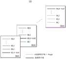
参照图23,SSD系统2300可包括主机2100和SSD 2200。SSD 2200可通过信号连接件2001与主机2100交换信号SIG,并通过电源连接件2002接收电力PWR。SSD 2200可包括SSD控制器2210、多个闪速存储器2221至222n、备用电源2230和缓冲存储器2240。Referring to FIG. 23 , an
SSD控制器2210可响应于从主机2100接收到的信号SIG控制多个闪速存储器2221至222n。例如,SSD控制器2210和多个闪速存储器2221至222n可包括参照图1至图22描述的存储器控制器和非易失性存储器装置。The
SSD控制器2210可包括刷新读控制器2212和提供SSD 2200的温度信息的温度传感器2214。刷新读控制器2212可控制闪速存储器2221至222n中包括的多个存储块中的每一个执行刷新读操作,该刷新读操作包括针对相应的存储块的多条字线之一的读操作。The
刷新读控制器2212可根据加强刷新读操作而同时地控制包括在闪速存储器2221至222n中的所有存储块连续地执行刷新读操作。刷新读控制器2212可根据普通刷新读操作而在刷新读间隔期间控制包括在闪速存储器2221至222n中的所有存储块顺序地执行刷新读操作。The refresh read
刷新读控制器2212可根据温度传感器2214的温度信息来改变普通刷新读操作的刷新读取间隔。可替换地,刷新读控制器2212可根据包括在闪速存储器2221至222n中的所有存储块的总可用量、有效数据量、数据分布状态或取决于编程和擦除P/E操作的损耗水平来改变刷新读间隔。The refresh read
备用电源2230可通过电源连接件2002连接至主机2100。备用电源2230可利用从主机2100接收的电力PWR充电。备用电源2230可在主机2100没有正常地供电时为SSD系统2300提供电力。例如,备用电源2230可放置在SSD 2200内或放置在SSD 2200外。例如,备用电源2230可放置在SSD系统2300的主板中,并且可向SSD 2200供应备用电力。A
SSD 2200可在突然断电期间通过使用充在备用电源2230中的电力PWR执行闪速存储器2221至222n的刷新读操作。The
缓冲存储器2240可作为SSD 2200的缓冲存储器进行操作。例如,缓冲存储器2240可临时地存储从主机2100或闪速存储器2221至222n接收的数据,或者可临时地存储实现为软件层的刷新读控制器2212。例如,刷新读控制器2212可实现为固件并存储在闪速存储器2221至222n的若干个中。The
图24是示出应用了根据本公开实施例的执行刷新读操作的存储系统的通用闪速存储(UFS)系统2400的示例的框图。24 is a block diagram illustrating an example of a Universal Flash Storage (UFS)
参照图24,UFS系统2400可包括UFS主机2410和UFS装置2420。UFS主机2410和UFS装置2420可通过UFS接口2430相连接。UFS 系统2400可基于作为非易失性存储器装置的闪速存储器,并且可主要用于诸如智能电话的移动装置中。24 , the
UFS主机2410可包括应用2412、装置驱动器2414、主机控制器2416和主机接口2418。应用2412可为在UFS主机2410中执行的各种应用程序。设备驱动器2414可用于驱动连接至UFS主机2410并在UFS主机2410中使用的外围设备,并且可驱动UFS装置2420。应用2412和装置驱动器2414可通过软件、固件等实现。
主机控制器2416可根据应用2412和装置驱动器2414的请求生成要提供给UFS装置2420的协议或命令,并且通过主机接口2418向UFS设备2420提供所生成的命令。主机控制器2416可在接收到来自装置驱动器2414的写请求时通过主机接口2418向UFS装置2420提供写命令和数据,在接收到来自装置驱动器2414的读请求时通过主机接口2418向UFS装置2420提供读命令,并从UFS装置2420接收数据。The
UFS装置2420可通过装置接口2421连接至UFS主机2410。主机接口2418和装置接口2421可通过用于发送和接收数据的数据线或者通过用于提供电力的电源线相连接。The
UFS装置2420可包括装置控制器2422、缓冲存储器2424和非易失性存储器装置2426。装置控制器2422可控制非易失性存储器装置2426的全部操作,例如写操作、读操作、擦除操作等。装置控制器2422可通过地址和数据总线与缓冲存储器2424或非易失性存储器装置2426交换数据。装置控制器2422可包括CPU、装置直接存储器存取(DMA)、闪速DMA、命令管理器、缓冲管理器、闪存转换层(FTL)、闪存管理器等。
UFS装置2420可通过装置接口2421将从UFS主机2410接收的命令提供给装置DMA和命令管理器。命令管理器可指定缓冲存储器2424以通过缓冲管理器接收数据,并在数据传输准备完成时向UFS主机2410发送响应信号。The
UFS主机2410可响应于响应信号向UFS装置2420发送数据。UFS装置2420可通过装置DMA和缓冲管理器将发送的数据存储在缓冲存 储器2424中。存储在缓冲存储器2424中的数据可通过闪速DMA提供给闪存管理器。闪存管理器可参照FTL的地址映射信息将数据存储在非易失性存储器装置2426的所选择的地址。The
当UFS主机2410的命令所需的数据传输和程序完成时,UFS装置2420可向UFS主机2410发送响应信号,并且通过装置接口2421向UFS主机2410通知命令完成。UFS主机2410可通知装置驱动器2414和应用2412是否完成了命令的响应信号的接收,并结束相应的命令。When the data transfer and program required by the command of the
UFS系统2400中包括的装置控制器2422和非易失性存储器装置2426可包括参照图1至图22描述的存储器控制器和非易失性存储器装置。装置控制器2422可包括刷新读控制器2423。刷新读控制器2423可控制非易失性存储器装置2426中包括的多个存储块中的每一个执行刷新读操作,该刷新读操作包括针对相应的存储块的多条字线之一的读操作。The
刷新读控制器2423可根据加强刷新读操作而同时地控制包括在非易失性存储器装置2426中的所有存储块连续地执行刷新读操作。刷新读控制器2212可根据普通刷新读操作而在刷新读间隔期间控制包括在非易失性存储器装置2426中的所有存储块顺序地执行刷新读操作。The refresh read
图25是用于描述图24的UFS接口2430的示图。FIG. 25 is a diagram for describing the
参照图25,UFS接口2430可使用SATA接口。SATA接口可主要分为物理层、链路层和传输层。Referring to FIG. 25, the
链路层和传输层可将用于传输数据的信息数据转换为包数据并将包数据传送至物理层。链路层和传输层可从由物理层传送的信号提取信息数据,并将所提取的信息数据传送至作为上层的应用层。物理层可将从链路层传送的包数据转换为电子信号,并将该电子信号以高速发送至外部。物理层可将从外部接收的信号传送至链路层。为此,物理层可构造为模拟电路,并且链路层和传输层可构造为数字电路。The link layer and the transport layer can convert information data for transmitting data into packet data and transmit the packet data to the physical layer. The link layer and the transport layer can extract information data from the signal transmitted by the physical layer and transmit the extracted information data to the application layer which is an upper layer. The physical layer converts packet data transferred from the link layer into electrical signals and transmits the electrical signals to the outside at high speed. The physical layer can transmit signals received from the outside to the link layer. For this purpose, the physical layer can be constructed as an analog circuit, and the link layer and the transport layer can be constructed as a digital circuit.
SATA接口的物理层(即,模拟电路)可认定为模拟前端。SATA接口的模拟前端可构造为用于将模拟信号转换为数字信号或将数字信号转换为模拟信号的物理块。The physical layer (ie, the analog circuitry) of the SATA interface can be identified as an analog front end. The analog front end of the SATA interface may be constructed as a physical block for converting analog signals to digital signals or converting digital signals to analog signals.
在图25中,主机SATA接口2418可包括发射器2511和接收器2514,并且UFS装置SATA接口2421可包括接收器2512和发射器2513。发射器2511和2513以及接收器2512和2514可对应于SATA接口的物理层。主机SATA接口2418的发射器2511可连接至UFS装置SATA接口2421的接收器2512。UFS装置SATA接口2421的发射器2513可连接至主机SATA接口2418的接收器2514。主机SATA接口2418和UFS装置SATA接口2421可通过构造为用于传输差分信号Tx+和Tx-或Rx+和Rx-的两对单向数据线的SATA线缆彼此连接。In FIG. 25 , the
图26是用于描述通过SATA接口执行的差分信号传输方法的示图。FIG. 26 is a diagram for describing a differential signaling method performed through a SATA interface.
参照图26,在SATA接口中,数据传输可表示为等于通过数据线传输的两个信号Tx+和Tx-或者Rx+和Rx-之间的差的数据值。在没有数据传输的阶段,两个信号均可保持在中间逻辑状态或浮空状态。例如,在没有数据传输的阶段,两个信号可为共模电压电平。Referring to FIG. 26, in a SATA interface, data transfer may be expressed as a data value equal to the difference between two signals Tx+ and Tx- or Rx+ and Rx- transferred through a data line. During periods of no data transfer, both signals can remain in an intermediate logic state or float. For example, during periods of no data transmission, the two signals may be at a common mode voltage level.
图27是用于描述通过SATA接口执行的电源管理方法的示图。FIG. 27 is a diagram for describing a power management method performed through a SATA interface.
参照图24和图27,SATA接口的协议可定义物理层就绪状态(下面称作“PHYRDY状态”)。SATA接口的协议可定义用于在省电模式下运转的SATA接口的部分状态和睡眠(slumber)状态。PHYRDY状态、部分状态和睡眠状态可为在SATA规范中定义的加电状态。24 and 27, the protocol of the SATA interface may define a physical layer ready state (hereinafter referred to as "PHYRDY state"). The protocol of the SATA interface may define partial states and slumber states for the SATA interface to operate in a power saving mode. The PHYRDY state, partial state, and sleep state may be power-on states defined in the SATA specification.
PHYRDY状态可指激活物理层的所有物理块的状态。部分状态和睡眠状态可指SATA接口基本没有工作的省电模式。也就是说,部分状态和睡眠状态可指没有向物理层的一些物理块供电的状态。The PHYRDY state may refer to the state of all physical blocks of the active physical layer. The partial state and the sleep state may refer to a power saving mode in which the SATA interface basically does not work. That is, the partial state and the sleep state may refer to states in which power is not supplied to some physical blocks of the physical layer.
可通过将SATA接口从相应模式恢复为PHYRDY状态所花费的唤醒时间及功耗来将部分状态和睡眠状态彼此区分开。在部分状态下,可不向数据发送和接收相关的物理块供电。在睡眠状态下,可不向除静噪电路之外的所有物理块供电。因此,考虑到PHYRDY状态唤醒的时间,部分状态可比睡眠状态恢复得更快。SATA接口在睡眠状态下的功耗可小于SATA接口在部分状态下的功耗。Partial states and sleep states can be distinguished from each other by the wake-up time and power consumption it takes to restore the SATA interface from the corresponding mode to the PHYRDY state. In some states, power may not be supplied to physical blocks related to data transmission and reception. In the sleep state, power may not be supplied to all physical blocks except the squelch circuit. Therefore, some states can resume faster than sleep states, taking into account the time to wake up from the PHYRDY state. The power consumption of the SATA interface in the sleep state may be smaller than the power consumption of the SATA interface in some states.
SATA接口2430可为电源管理方法并且可支持初始化电源管理(IPM)功能。IPM可分为主机IPM(HIPM)和装置IPM(DIPM)。HIPM 根据主机SATA接口2418的请求改变主机SATA接口2418和UFS装置SATA接口2421的电源状态。DIPM根据UFS装置SATA接口2421的请求改变主机SATA接口2418和UFS装置SATA接口2421的电源状态。The
想要工作在省电模式下的主机SATA接口2418可通过使用HIPM向UFS装置SATA接口2421发送省电模式请求信号。接收到省电模式请求信号的UFS装置SATA接口2421可在可进入省电模式时向主机SATA接口2418发送响应信号。通过这种处理,主机SATA接口2418和UFS装置SATA接口2421可工作在省电模式下。也就是说,主机SATA接口2418和UFS装置SATA接口2421可保持部分状态和睡眠状态之一。The
在省电模式期间,想要工作在活动模式下的主机SATA接口2418可发送用于退出节电模式的请求信号,并且可执行用于与SATA接口2430形成通信链路的带外(OOB)信令。OOB信令也可在上电序列操作期间执行。通过这种处理,主机SATA接口2418和UFS装置SATA接口2421可工作在活动模式下。During the power saving mode, the
图28是用于描述在省电模式下通过图24的UFS装置2420执行的加强刷新读操作的示图。FIG. 28 is a diagram for describing an enhanced refresh read operation performed by the
参照图24、图27和图28,主机SATA接口2418和UFS装置SATA接口2421可检测没有命令发送的空闲阶段。如果命令空闲阶段大于预设时间(例如,60ms),则主机SATA接口2418可将请求UFS装置SATA接口2421工作在省电模式(例如,睡眠状态)下的信号PMREQ发送至UFS装置SATA接口2421。24 , 27 and 28 , the
如果主机SATA接口2418向UFS装置SATA接口2421发送省电模式请求信号PMREQ,则接收到省电模式请求信号PMREQ的UFS装置SATA接口2421可在可进入省电模式时向主机SATA接口2418发送响应信号PMACK。UFS装置2420可响应于睡眠状态的省电模式请求信号PMREQ执行非易失性存储器装置2426的加强刷新读操作。如果非易失性存储器装置2426的加强刷新读操作完成,则UFS装置SATA接口2421可向主机SATA接口2418发送用于指示可进入省电模式的响应信号PMACK。If the
例如,当非易失性存储器装置2426的加强刷新读操作开始时,UFS装置SATA接口2421可向SATA接口2418发送等待信号WAIT。等待信号WAIT可通知主机SATA接口2418将首先执行UFS装置2420的加强刷新读操作。For example, the UFS
图29是用于描述通过图24的UFS系统2400执行的刷新读操作的示图。FIG. 29 is a diagram for describing a refresh read operation performed by the
参照图24和图29,当UFS系统2400上电时,UFS装置2420可执行同时连续地刷新读取非易失性存储器装置2426的所有存储块的加强刷新读操作。24 and 29, when the
在UFS系统2400上电后,UFS装置2420可执行以刷新读间隔RDD_I顺序地刷新读取非易失性存储器装置2426的存储块的普通刷新读操作。After the
UFS装置2420可根据主机2410的省电模式请求响应于睡眠状态的省电模式请求信号PMREQ来同时执行连续地刷新读取非易失性存储器装置2426的所有存储块的加强刷新读操作。如果非易失性存储器装置2426的加强刷新读操作完成,则UFS装置2420可向主机2410发送用于指示可进入省电模式的响应信号PMACK。随后,UFS装置2420可变为不向各模块供电的休眠模式,从而可减少功耗。The
当UFS系统2400断电时,UFS装置2420可同时执行连续地刷新读取非易失性存储器装置2426的所有存储块的加强刷新读操作。例如,在突然断电期间,UFS装置2420可通过使用充在UFS装置2420的备用电源中的备用电力来执行加强刷新读操作。When the
本公开的上述实施例不仅可实现为装置和方法,还可实现为实现与本公开实施例的各部件相对应的功能的程序或者通过记录有程序的记录介质实现。本领域普通技术人员之一可根据上述说明容易地完成这种实现。The above-described embodiments of the present disclosure can be implemented not only as apparatuses and methods, but also as programs implementing functions corresponding to the respective components of the embodiments of the present disclosure or through a recording medium on which the programs are recorded. Such an implementation can be easily accomplished by one of ordinary skill in the art based on the above description.
如本领域中常规的那样,实施例可以按照实行所描述的一个功能或多个功能的块的方式描述和示意。利用诸如逻辑门、集成电路、微处理器、微控制器、存储器电路、无源电子部件、有源电子部件、光学部件、硬线电路等的模拟和/或数字电路来物理地实现此处可称 作单元或模块等的这些块,并且可以可选地通过固件和/或软件进行驱动。例如,电路可实施在一个或多个半导体芯片中或在诸如印刷电路板等的衬底支承件上。可通过专用硬件、或通过处理器(例如,一个或多个经编程的微处理器和相关电路)、或通过用以执行块的一些功能的专用电路与用以执行该块的其它功能的处理器的组合来实现构成该块的电路。实施例的每个块可物理地分为两个或更多个交互的独立块,而没有脱离本公开的范围。同样,实施例的块可物理地组合为更多复合块,而没有脱离本公开的范围。Embodiments may be described and illustrated in terms of blocks that perform the described function or functions, as is conventional in the art. physically implemented using analog and/or digital circuits such as logic gates, integrated circuits, microprocessors, microcontrollers, memory circuits, passive electronic components, active electronic components, optical components, hard-wired circuits, etc. These blocks are called units or modules, etc., and may optionally be driven by firmware and/or software. For example, the circuit may be implemented in one or more semiconductor chips or on a substrate support such as a printed circuit board or the like. Processing may be by dedicated hardware, or by a processor (eg, one or more programmed microprocessors and associated circuits), or by dedicated circuitry to perform some functions of a block and processing to perform other functions of the block A combination of devices is used to implement the circuits that make up the block. Each block of the embodiments may be physically divided into two or more interacting independent blocks without departing from the scope of this disclosure. Likewise, the blocks of an embodiment may be physically combined into more composite blocks without departing from the scope of this disclosure.
虽然已经参考本公开实施例具体示出并说明了本公开,但应当理解的是,在不脱离所附权利要求的精神和范围的情况下,其中可作出各种形式和细节上的修改。While the present disclosure has been particularly shown and described with reference to embodiments of the disclosure, it will be understood that various changes in form and details may be made therein without departing from the spirit and scope of the appended claims.
Claims (20)
Translated fromChineseApplications Claiming Priority (2)
| Application Number | Priority Date | Filing Date | Title |
|---|---|---|---|
| KR1020160061431AKR102644275B1 (en) | 2016-05-19 | 2016-05-19 | Operation method of memory controller for controlling non-volatile memory device with refresh read |
| KR10-2016-0061431 | 2016-05-19 |
Publications (2)
| Publication Number | Publication Date |
|---|---|
| CN107403639A CN107403639A (en) | 2017-11-28 |
| CN107403639Btrue CN107403639B (en) | 2020-12-11 |
Family
ID=60330383
Family Applications (1)
| Application Number | Title | Priority Date | Filing Date |
|---|---|---|---|
| CN201710201596.5AActiveCN107403639B (en) | 2016-05-19 | 2017-03-30 | How to operate the memory controller |
Country Status (3)
| Country | Link |
|---|---|
| US (1) | US9984757B2 (en) |
| KR (1) | KR102644275B1 (en) |
| CN (1) | CN107403639B (en) |
Families Citing this family (29)
| Publication number | Priority date | Publication date | Assignee | Title |
|---|---|---|---|---|
| US11955187B2 (en)* | 2017-01-13 | 2024-04-09 | Pure Storage, Inc. | Refresh of differing capacity NAND |
| US10289341B2 (en)* | 2017-06-30 | 2019-05-14 | Western Digital Technologies, Inc. | Operating parameter offsets in solid state memory devices |
| US10277435B2 (en) | 2017-08-07 | 2019-04-30 | Micron Technology, Inc. | Method to vertically align multi-level cells |
| US10447512B2 (en) | 2017-08-07 | 2019-10-15 | Micron Technology, Inc. | Channel equalization for multi-level signaling |
| US10403337B2 (en) | 2017-08-07 | 2019-09-03 | Micron Technology, Inc. | Output driver for multi-level signaling |
| US10425260B2 (en)* | 2017-08-07 | 2019-09-24 | Micron Technology, Inc. | Multi-level signaling in memory with wide system interface |
| US10530617B2 (en) | 2017-08-07 | 2020-01-07 | Micron Technology, Inc. | Programmable channel equalization for multi-level signaling |
| KR102244921B1 (en)* | 2017-09-07 | 2021-04-27 | 삼성전자주식회사 | Storage device and Method for refreshing thereof |
| JP6837419B2 (en)* | 2017-12-05 | 2021-03-03 | ルネサスエレクトロニクス株式会社 | Semiconductor storage device and refresh method for semiconductor storage device |
| CN109901785B (en)* | 2017-12-08 | 2022-04-05 | 华为云计算技术有限公司 | Command sequencing method, method for reducing read latency, and SSD controller for solid-state hard disks |
| KR102518370B1 (en)* | 2018-01-19 | 2023-04-05 | 삼성전자주식회사 | Storage device and debugging system thereof |
| KR20190106008A (en)* | 2018-03-07 | 2019-09-18 | 에스케이하이닉스 주식회사 | Memory system, operating method thereof and electronic device |
| KR20190108788A (en)* | 2018-03-15 | 2019-09-25 | 에스케이하이닉스 주식회사 | Memory system and operation method thereof |
| US10128842B1 (en) | 2018-03-23 | 2018-11-13 | Micron Technology, Inc. | Output impedance calibration for signaling |
| CN110838314A (en)* | 2018-08-17 | 2020-02-25 | 北京兆易创新科技股份有限公司 | Method and device for reinforcing stored data |
| KR102617411B1 (en)* | 2018-08-31 | 2023-12-26 | 에스케이하이닉스 주식회사 | Memory system and operation method thereof |
| KR102645740B1 (en)* | 2018-10-30 | 2024-03-11 | 에스케이하이닉스 주식회사 | Storage device and operating method thereof |
| KR102211122B1 (en)* | 2018-12-20 | 2021-02-02 | 삼성전자주식회사 | Storage device and storage system |
| KR102683296B1 (en)* | 2019-05-17 | 2024-07-10 | 에스케이하이닉스 주식회사 | Memory device and operating method thereof |
| KR102629487B1 (en)* | 2019-05-28 | 2024-01-26 | 에스케이하이닉스 주식회사 | Memory controller and operating method thereof |
| US11153231B2 (en)* | 2019-07-19 | 2021-10-19 | Arm Limited | Apparatus and method for processing flush requests within a packet network |
| US11061768B1 (en)* | 2020-02-14 | 2021-07-13 | Western Digital Technologies, Inc. | Storage device with increased endurance |
| KR102848954B1 (en) | 2020-02-28 | 2025-08-20 | 삼성전자주식회사 | Storage device and Method of operating the storage device |
| US11404127B1 (en) | 2021-02-11 | 2022-08-02 | Sandisk Technologies Llc | Read refresh to improve power on data retention for a non-volatile memory |
| US12205627B2 (en)* | 2021-08-04 | 2025-01-21 | Micron Technology, Inc. | Interface for refreshing non-volatile memory |
| US11687260B2 (en) | 2021-08-10 | 2023-06-27 | Micron Technology, Inc. | Pre-shutdown media management operation for vehicle memory sub-system |
| CN114036096B (en)* | 2021-11-04 | 2024-05-03 | 珠海一微半导体股份有限公司 | Read controller based on bus interface |
| KR20230072336A (en) | 2021-11-17 | 2023-05-24 | 에스케이하이닉스 주식회사 | Semiconductor device |
| US11797215B2 (en) | 2021-12-09 | 2023-10-24 | SK Hynix Inc. | Memory device and memory system performing error check and scrub operation |
Citations (4)
| Publication number | Priority date | Publication date | Assignee | Title |
|---|---|---|---|---|
| US5768193A (en)* | 1996-06-17 | 1998-06-16 | Aplus Integrated Circuits, Inc. | Bit-refreshable method and circuit for refreshing a nonvolatile flash memory |
| US8243525B1 (en)* | 2009-09-30 | 2012-08-14 | Western Digital Technologies, Inc. | Refreshing non-volatile semiconductor memory by reading without rewriting |
| CN102881329A (en)* | 2011-07-12 | 2013-01-16 | 三星电子株式会社 | Erase system and method of nonvolatile memory device |
| CN104036825A (en)* | 2013-03-07 | 2014-09-10 | 三星电子株式会社 | Memory Controller And Memory System Including The Same |
Family Cites Families (9)
| Publication number | Priority date | Publication date | Assignee | Title |
|---|---|---|---|---|
| KR100524059B1 (en)* | 1998-10-01 | 2005-12-21 | 삼성전자주식회사 | ST. Computer's ST. Function support device |
| US7447096B2 (en) | 2006-05-05 | 2008-11-04 | Honeywell International Inc. | Method for refreshing a non-volatile memory |
| US8938655B2 (en) | 2007-12-20 | 2015-01-20 | Spansion Llc | Extending flash memory data retension via rewrite refresh |
| US8281061B2 (en) | 2008-03-31 | 2012-10-02 | Micron Technology, Inc. | Data conditioning to improve flash memory reliability |
| US8443221B2 (en) | 2011-03-04 | 2013-05-14 | Sandisk Technologies Inc. | Methods, systems, and computer readable media for advanced power management for serial advanced technology attachment (SATA)-based storage devices |
| US8972652B2 (en) | 2012-11-19 | 2015-03-03 | Spansion Llc | Data refresh in non-volatile memory |
| US9627085B2 (en) | 2012-11-29 | 2017-04-18 | Silicon Motion Inc. | Refresh method for flash memory and related memory controller thereof |
| US9342401B2 (en) | 2013-09-16 | 2016-05-17 | Sandisk Technologies Inc. | Selective in-situ retouching of data in nonvolatile memory |
| KR102110767B1 (en) | 2013-12-24 | 2020-06-09 | 삼성전자 주식회사 | Operating method of memory controller and the memory controller |
- 2016
- 2016-05-19KRKR1020160061431Apatent/KR102644275B1/enactiveActive
- 2016-11-15USUS15/351,576patent/US9984757B2/enactiveActive
- 2017
- 2017-03-30CNCN201710201596.5Apatent/CN107403639B/enactiveActive
Patent Citations (4)
| Publication number | Priority date | Publication date | Assignee | Title |
|---|---|---|---|---|
| US5768193A (en)* | 1996-06-17 | 1998-06-16 | Aplus Integrated Circuits, Inc. | Bit-refreshable method and circuit for refreshing a nonvolatile flash memory |
| US8243525B1 (en)* | 2009-09-30 | 2012-08-14 | Western Digital Technologies, Inc. | Refreshing non-volatile semiconductor memory by reading without rewriting |
| CN102881329A (en)* | 2011-07-12 | 2013-01-16 | 三星电子株式会社 | Erase system and method of nonvolatile memory device |
| CN104036825A (en)* | 2013-03-07 | 2014-09-10 | 三星电子株式会社 | Memory Controller And Memory System Including The Same |
Also Published As
| Publication number | Publication date |
|---|---|
| CN107403639A (en) | 2017-11-28 |
| US20170337979A1 (en) | 2017-11-23 |
| KR102644275B1 (en) | 2024-03-06 |
| US9984757B2 (en) | 2018-05-29 |
| KR20170130788A (en) | 2017-11-29 |
Similar Documents
| Publication | Publication Date | Title |
|---|---|---|
| CN107403639B (en) | How to operate the memory controller | |
| CN107068190B (en) | Memory device programming method with program voltage correction | |
| US9858993B2 (en) | Non-volatile memory device and method of programming the same | |
| US9805807B2 (en) | Operation method operating nonvolatile memory device having plurality of memory blocks | |
| CN107154274B (en) | Method of operating a non-volatile memory device | |
| US9910607B2 (en) | Method of managing a memory, and a memory system | |
| CN103632720A (en) | Nonvolatile memory device and data processing method | |
| CN111798904A (en) | Nonvolatile memory device, method of operating the same, and memory system | |
| US9589640B2 (en) | Data storage device including nonvolatile memory device and operating method thereof | |
| CN110390984A (en) | Memory system and method of operation of the memory system | |
| KR20220075684A (en) | Memory system and operating method of memory system | |
| US12217801B2 (en) | Bias voltage schemes during pre-programming and programming phases | |
| US20230207019A1 (en) | Multi-level cell and multi-sub-block programming in a memory device | |
| CN115705905A (en) | Tracking RC time constant by word line in memory device | |
| CN114582401A (en) | Method of writing data in nonvolatile memory device, and method of operating memory system | |
| US20240312525A1 (en) | Re-driving data to a sub-block during programming of multiple sub-blocks | |
| US12406731B2 (en) | Dynamic latches above a three-dimensional non-volatile memory array | |
| US9570181B2 (en) | Memory system | |
| US12387790B2 (en) | Double single level cell program in a memory device | |
| CN111798903B (en) | Memory system, memory device, and memory controller | |
| US12272421B2 (en) | Creating dynamic latches above a three-dimensional non-volatile memory array | |
| US12027210B2 (en) | Programming delay scheme for a memory sub-system based on memory reliability | |
| KR102847403B1 (en) | Apparatus and method for improving data retention ability of nonvolatile memory device | |
| US20240428862A1 (en) | Seeding bias control for sub-block groups in a memory device | |
| US11742036B2 (en) | Reducing maximum programming voltage in memory programming operations |
Legal Events
| Date | Code | Title | Description |
|---|---|---|---|
| PB01 | Publication | ||
| PB01 | Publication | ||
| SE01 | Entry into force of request for substantive examination | ||
| SE01 | Entry into force of request for substantive examination | ||
| GR01 | Patent grant | ||
| GR01 | Patent grant |