CN107342300B - Semiconductor device and method of manufacturing image sensor device - Google Patents
Semiconductor device and method of manufacturing image sensor deviceDownload PDFInfo
- Publication number
- CN107342300B CN107342300BCN201611155540.2ACN201611155540ACN107342300BCN 107342300 BCN107342300 BCN 107342300BCN 201611155540 ACN201611155540 ACN 201611155540ACN 107342300 BCN107342300 BCN 107342300B
- Authority
- CN
- China
- Prior art keywords
- layer
- pixel region
- coating
- photodiode
- thickness
- Prior art date
- Legal status (The legal status is an assumption and is not a legal conclusion. Google has not performed a legal analysis and makes no representation as to the accuracy of the status listed.)
- Active
Links
- 239000004065semiconductorSubstances0.000titleclaimsabstractdescription52
- 238000004519manufacturing processMethods0.000titleclaimsabstractdescription8
- 239000006117anti-reflective coatingSubstances0.000claimsabstractdescription242
- 239000000758substrateSubstances0.000claimsabstractdescription103
- 238000000034methodMethods0.000claimsabstractdescription83
- 239000010410layerSubstances0.000claimsdescription183
- 239000000463materialSubstances0.000claimsdescription147
- 239000011248coating agentSubstances0.000claimsdescription58
- 238000000576coating methodMethods0.000claimsdescription58
- 239000003989dielectric materialSubstances0.000claimsdescription36
- 238000000151depositionMethods0.000claimsdescription31
- 229910052581Si3N4Inorganic materials0.000claimsdescription30
- HQVNEWCFYHHQES-UHFFFAOYSA-Nsilicon nitrideChemical compoundN12[Si]34N5[Si]62N3[Si]51N64HQVNEWCFYHHQES-UHFFFAOYSA-N0.000claimsdescription30
- 150000002500ionsChemical class0.000claimsdescription14
- 239000007943implantSubstances0.000claimsdescription11
- 230000008021depositionEffects0.000claimsdescription5
- 150000004767nitridesChemical class0.000claimsdescription4
- 230000003667anti-reflective effectEffects0.000claims7
- 239000011247coating layerSubstances0.000claims1
- 230000008569processEffects0.000description35
- 229920002120photoresistant polymerPolymers0.000description20
- 238000005530etchingMethods0.000description18
- 229910052814silicon oxideInorganic materials0.000description18
- VYPSYNLAJGMNEJ-UHFFFAOYSA-NSilicium dioxideChemical compoundO=[Si]=OVYPSYNLAJGMNEJ-UHFFFAOYSA-N0.000description17
- 239000002243precursorSubstances0.000description17
- 230000015572biosynthetic processEffects0.000description15
- 238000005229chemical vapour depositionMethods0.000description11
- 238000005286illuminationMethods0.000description11
- 238000000206photolithographyMethods0.000description11
- 239000003086colorantSubstances0.000description9
- 125000006850spacer groupChemical group0.000description9
- 229910052751metalInorganic materials0.000description7
- 239000002184metalSubstances0.000description7
- 230000003287optical effectEffects0.000description7
- 238000002513implantationMethods0.000description6
- 238000002955isolationMethods0.000description6
- TWNQGVIAIRXVLR-UHFFFAOYSA-Noxo(oxoalumanyloxy)alumaneChemical compoundO=[Al]O[Al]=OTWNQGVIAIRXVLR-UHFFFAOYSA-N0.000description6
- 238000012546transferMethods0.000description6
- 206010001513AIDS related complexDiseases0.000description5
- XUIMIQQOPSSXEZ-UHFFFAOYSA-NSiliconChemical compound[Si]XUIMIQQOPSSXEZ-UHFFFAOYSA-N0.000description5
- 229910000577Silicon-germaniumInorganic materials0.000description5
- 210000002945adventitial reticular cellAnatomy0.000description5
- 239000002019doping agentSubstances0.000description5
- 239000000203mixtureSubstances0.000description5
- 230000003647oxidationEffects0.000description5
- 238000007254oxidation reactionMethods0.000description5
- 238000000623plasma-assisted chemical vapour depositionMethods0.000description5
- 229910021420polycrystalline siliconInorganic materials0.000description5
- 229910052710siliconInorganic materials0.000description5
- 239000010703siliconSubstances0.000description5
- HBMJWWWQQXIZIP-UHFFFAOYSA-Nsilicon carbideChemical compound[Si+]#[C-]HBMJWWWQQXIZIP-UHFFFAOYSA-N0.000description5
- 229910010271silicon carbideInorganic materials0.000description5
- QGZKDVFQNNGYKY-UHFFFAOYSA-NAmmoniaChemical compoundNQGZKDVFQNNGYKY-UHFFFAOYSA-N0.000description4
- LEVVHYCKPQWKOP-UHFFFAOYSA-N[Si].[Ge]Chemical compound[Si].[Ge]LEVVHYCKPQWKOP-UHFFFAOYSA-N0.000description4
- 230000004888barrier functionEffects0.000description4
- 239000004020conductorSubstances0.000description4
- 238000002161passivationMethods0.000description4
- 229920005591polysiliconPolymers0.000description4
- BOTDANWDWHJENH-UHFFFAOYSA-NTetraethyl orthosilicateChemical compoundCCO[Si](OCC)(OCC)OCCBOTDANWDWHJENH-UHFFFAOYSA-N0.000description3
- CJNBYAVZURUTKZ-UHFFFAOYSA-Nhafnium(iv) oxideChemical compoundO=[Hf]=OCJNBYAVZURUTKZ-UHFFFAOYSA-N0.000description3
- 238000004518low pressure chemical vapour depositionMethods0.000description3
- 229910021332silicideInorganic materials0.000description3
- FVBUAEGBCNSCDD-UHFFFAOYSA-Nsilicide(4-)Chemical compound[Si-4]FVBUAEGBCNSCDD-UHFFFAOYSA-N0.000description3
- 229910052715tantalumInorganic materials0.000description3
- GUVRBAGPIYLISA-UHFFFAOYSA-Ntantalum atomChemical compound[Ta]GUVRBAGPIYLISA-UHFFFAOYSA-N0.000description3
- WFKWXMTUELFFGS-UHFFFAOYSA-NtungstenChemical compound[W]WFKWXMTUELFFGS-UHFFFAOYSA-N0.000description3
- 229910052721tungstenInorganic materials0.000description3
- 239000010937tungstenSubstances0.000description3
- JBRZTFJDHDCESZ-UHFFFAOYSA-NAsGaChemical compound[As]#[Ga]JBRZTFJDHDCESZ-UHFFFAOYSA-N0.000description2
- GYHNNYVSQQEPJS-UHFFFAOYSA-NGalliumChemical compound[Ga]GYHNNYVSQQEPJS-UHFFFAOYSA-N0.000description2
- 229910001218Gallium arsenideInorganic materials0.000description2
- GPXJNWSHGFTCBW-UHFFFAOYSA-NIndium phosphideChemical compound[In]#PGPXJNWSHGFTCBW-UHFFFAOYSA-N0.000description2
- -1SOIChemical compound0.000description2
- BLRPTPMANUNPDV-UHFFFAOYSA-NSilaneChemical compound[SiH4]BLRPTPMANUNPDV-UHFFFAOYSA-N0.000description2
- RTAQQCXQSZGOHL-UHFFFAOYSA-NTitaniumChemical compound[Ti]RTAQQCXQSZGOHL-UHFFFAOYSA-N0.000description2
- NRTOMJZYCJJWKI-UHFFFAOYSA-NTitanium nitrideChemical compound[Ti]#NNRTOMJZYCJJWKI-UHFFFAOYSA-N0.000description2
- 229910052782aluminiumInorganic materials0.000description2
- XAGFODPZIPBFFR-UHFFFAOYSA-NaluminiumChemical compound[Al]XAGFODPZIPBFFR-UHFFFAOYSA-N0.000description2
- 238000000137annealingMethods0.000description2
- 229910052787antimonyInorganic materials0.000description2
- WATWJIUSRGPENY-UHFFFAOYSA-Nantimony atomChemical compound[Sb]WATWJIUSRGPENY-UHFFFAOYSA-N0.000description2
- 229910052785arsenicInorganic materials0.000description2
- RQNWIZPPADIBDY-UHFFFAOYSA-Narsenic atomChemical compound[As]RQNWIZPPADIBDY-UHFFFAOYSA-N0.000description2
- 239000005380borophosphosilicate glassSubstances0.000description2
- 230000000295complement effectEffects0.000description2
- 230000003247decreasing effectEffects0.000description2
- 238000009826distributionMethods0.000description2
- 229910052733galliumInorganic materials0.000description2
- 229910052732germaniumInorganic materials0.000description2
- GNPVGFCGXDBREM-UHFFFAOYSA-Ngermanium atomChemical compound[Ge]GNPVGFCGXDBREM-UHFFFAOYSA-N0.000description2
- 229910052735hafniumInorganic materials0.000description2
- VBJZVLUMGGDVMO-UHFFFAOYSA-Nhafnium atomChemical compound[Hf]VBJZVLUMGGDVMO-UHFFFAOYSA-N0.000description2
- 239000012212insulatorSubstances0.000description2
- MRELNEQAGSRDBK-UHFFFAOYSA-Nlanthanum(3+);oxygen(2-)Chemical compound[O-2].[O-2].[O-2].[La+3].[La+3]MRELNEQAGSRDBK-UHFFFAOYSA-N0.000description2
- 150000002739metalsChemical class0.000description2
- BASFCYQUMIYNBI-UHFFFAOYSA-NplatinumChemical compound[Pt]BASFCYQUMIYNBI-UHFFFAOYSA-N0.000description2
- 238000005498polishingMethods0.000description2
- 229920000642polymerPolymers0.000description2
- 230000009467reductionEffects0.000description2
- 238000004528spin coatingMethods0.000description2
- 239000000126substanceSubstances0.000description2
- MZLGASXMSKOWSE-UHFFFAOYSA-Ntantalum nitrideChemical compound[Ta]#NMZLGASXMSKOWSE-UHFFFAOYSA-N0.000description2
- 229910052719titaniumInorganic materials0.000description2
- 239000010936titaniumSubstances0.000description2
- PNEYBMLMFCGWSK-UHFFFAOYSA-NAluminaChemical compound[O-2].[O-2].[O-2].[Al+3].[Al+3]PNEYBMLMFCGWSK-UHFFFAOYSA-N0.000description1
- 101100207343Antirrhinum majus 1e20 geneProteins0.000description1
- IJGRMHOSHXDMSA-UHFFFAOYSA-NAtomic nitrogenChemical compoundN#NIJGRMHOSHXDMSA-UHFFFAOYSA-N0.000description1
- ZOXJGFHDIHLPTG-UHFFFAOYSA-NBoronChemical compound[B]ZOXJGFHDIHLPTG-UHFFFAOYSA-N0.000description1
- RYGMFSIKBFXOCR-UHFFFAOYSA-NCopperChemical compound[Cu]RYGMFSIKBFXOCR-UHFFFAOYSA-N0.000description1
- 229910000881Cu alloyInorganic materials0.000description1
- 229910000673Indium arsenideInorganic materials0.000description1
- ZOKXTWBITQBERF-UHFFFAOYSA-NMolybdenumChemical compound[Mo]ZOKXTWBITQBERF-UHFFFAOYSA-N0.000description1
- OAICVXFJPJFONN-UHFFFAOYSA-NPhosphorusChemical compound[P]OAICVXFJPJFONN-UHFFFAOYSA-N0.000description1
- KJTLSVCANCCWHF-UHFFFAOYSA-NRutheniumChemical compound[Ru]KJTLSVCANCCWHF-UHFFFAOYSA-N0.000description1
- KZNMRPQBBZBTSW-UHFFFAOYSA-N[Au]=OChemical compound[Au]=OKZNMRPQBBZBTSW-UHFFFAOYSA-N0.000description1
- 239000003082abrasive agentSubstances0.000description1
- 239000000853adhesiveSubstances0.000description1
- 230000001070adhesive effectEffects0.000description1
- 230000004075alterationEffects0.000description1
- 229910021529ammoniaInorganic materials0.000description1
- 229910021417amorphous siliconInorganic materials0.000description1
- 238000003491arrayMethods0.000description1
- 238000004380ashingMethods0.000description1
- QVGXLLKOCUKJST-UHFFFAOYSA-Natomic oxygenChemical compound[O]QVGXLLKOCUKJST-UHFFFAOYSA-N0.000description1
- 229910052796boronInorganic materials0.000description1
- 238000006243chemical reactionMethods0.000description1
- 229910017052cobaltInorganic materials0.000description1
- 239000010941cobaltSubstances0.000description1
- GUTLYIVDDKVIGB-UHFFFAOYSA-Ncobalt atomChemical compound[Co]GUTLYIVDDKVIGB-UHFFFAOYSA-N0.000description1
- 238000004891communicationMethods0.000description1
- 150000001875compoundsChemical class0.000description1
- 238000010276constructionMethods0.000description1
- 238000007796conventional methodMethods0.000description1
- 229910052802copperInorganic materials0.000description1
- 239000010949copperSubstances0.000description1
- 230000007547defectEffects0.000description1
- 229910003460diamondInorganic materials0.000description1
- 239000010432diamondSubstances0.000description1
- 230000009977dual effectEffects0.000description1
- 238000011049fillingMethods0.000description1
- 239000011521glassSubstances0.000description1
- 239000002241glass-ceramicSubstances0.000description1
- 229910001922gold oxideInorganic materials0.000description1
- 229910000449hafnium oxideInorganic materials0.000description1
- WIHZLLGSGQNAGK-UHFFFAOYSA-Nhafnium(4+);oxygen(2-)Chemical compound[O-2].[O-2].[Hf+4]WIHZLLGSGQNAGK-UHFFFAOYSA-N0.000description1
- BHEPBYXIRTUNPN-UHFFFAOYSA-Nhydridophosphorus(.) (triplet)Chemical compound[PH]BHEPBYXIRTUNPN-UHFFFAOYSA-N0.000description1
- RPQDHPTXJYYUPQ-UHFFFAOYSA-Nindium arsenideChemical compound[In]#[As]RPQDHPTXJYYUPQ-UHFFFAOYSA-N0.000description1
- 239000011229interlayerSubstances0.000description1
- 238000005468ion implantationMethods0.000description1
- 230000001788irregularEffects0.000description1
- 230000000873masking effectEffects0.000description1
- 229910052750molybdenumInorganic materials0.000description1
- 239000011733molybdenumSubstances0.000description1
- RUFLMLWJRZAWLJ-UHFFFAOYSA-Nnickel silicideChemical compound[Ni]=[Si]=[Ni]RUFLMLWJRZAWLJ-UHFFFAOYSA-N0.000description1
- 229910021334nickel silicideInorganic materials0.000description1
- 229910052760oxygenInorganic materials0.000description1
- 239000001301oxygenSubstances0.000description1
- RVTZCBVAJQQJTK-UHFFFAOYSA-Noxygen(2-);zirconium(4+)Chemical compound[O-2].[O-2].[Zr+4]RVTZCBVAJQQJTK-UHFFFAOYSA-N0.000description1
- 238000000059patterningMethods0.000description1
- 229910052698phosphorusInorganic materials0.000description1
- 239000011574phosphorusSubstances0.000description1
- 230000000704physical effectEffects0.000description1
- 239000000049pigmentSubstances0.000description1
- 238000002294plasma sputter depositionMethods0.000description1
- 229910052697platinumInorganic materials0.000description1
- 239000002861polymer materialSubstances0.000description1
- 239000002952polymeric resinSubstances0.000description1
- 238000012545processingMethods0.000description1
- 229920005989resinPolymers0.000description1
- 229910052707rutheniumInorganic materials0.000description1
- 229910000077silaneInorganic materials0.000description1
- 238000004088simulationMethods0.000description1
- 230000007480spreadingEffects0.000description1
- 238000003892spreadingMethods0.000description1
- 238000006467substitution reactionMethods0.000description1
- 229910021341titanium silicideInorganic materials0.000description1
- 229910052723transition metalInorganic materials0.000description1
- 150000003624transition metalsChemical class0.000description1
- 229910001928zirconium oxideInorganic materials0.000description1
Images


Classifications
- H—ELECTRICITY
- H10—SEMICONDUCTOR DEVICES; ELECTRIC SOLID-STATE DEVICES NOT OTHERWISE PROVIDED FOR
- H10F—INORGANIC SEMICONDUCTOR DEVICES SENSITIVE TO INFRARED RADIATION, LIGHT, ELECTROMAGNETIC RADIATION OF SHORTER WAVELENGTH OR CORPUSCULAR RADIATION
- H10F39/00—Integrated devices, or assemblies of multiple devices, comprising at least one element covered by group H10F30/00, e.g. radiation detectors comprising photodiode arrays
- H10F39/80—Constructional details of image sensors
- H10F39/805—Coatings
- H—ELECTRICITY
- H10—SEMICONDUCTOR DEVICES; ELECTRIC SOLID-STATE DEVICES NOT OTHERWISE PROVIDED FOR
- H10F—INORGANIC SEMICONDUCTOR DEVICES SENSITIVE TO INFRARED RADIATION, LIGHT, ELECTROMAGNETIC RADIATION OF SHORTER WAVELENGTH OR CORPUSCULAR RADIATION
- H10F39/00—Integrated devices, or assemblies of multiple devices, comprising at least one element covered by group H10F30/00, e.g. radiation detectors comprising photodiode arrays
- H10F39/011—Manufacture or treatment of image sensors covered by group H10F39/12
- H10F39/024—Manufacture or treatment of image sensors covered by group H10F39/12 of coatings or optical elements
- H—ELECTRICITY
- H10—SEMICONDUCTOR DEVICES; ELECTRIC SOLID-STATE DEVICES NOT OTHERWISE PROVIDED FOR
- H10F—INORGANIC SEMICONDUCTOR DEVICES SENSITIVE TO INFRARED RADIATION, LIGHT, ELECTROMAGNETIC RADIATION OF SHORTER WAVELENGTH OR CORPUSCULAR RADIATION
- H10F39/00—Integrated devices, or assemblies of multiple devices, comprising at least one element covered by group H10F30/00, e.g. radiation detectors comprising photodiode arrays
- H10F39/10—Integrated devices
- H10F39/12—Image sensors
- H10F39/18—Complementary metal-oxide-semiconductor [CMOS] image sensors; Photodiode array image sensors
- H10F39/182—Colour image sensors
- H—ELECTRICITY
- H10—SEMICONDUCTOR DEVICES; ELECTRIC SOLID-STATE DEVICES NOT OTHERWISE PROVIDED FOR
- H10F—INORGANIC SEMICONDUCTOR DEVICES SENSITIVE TO INFRARED RADIATION, LIGHT, ELECTROMAGNETIC RADIATION OF SHORTER WAVELENGTH OR CORPUSCULAR RADIATION
- H10F39/00—Integrated devices, or assemblies of multiple devices, comprising at least one element covered by group H10F30/00, e.g. radiation detectors comprising photodiode arrays
- H10F39/10—Integrated devices
- H10F39/12—Image sensors
- H10F39/199—Back-illuminated image sensors
- H—ELECTRICITY
- H10—SEMICONDUCTOR DEVICES; ELECTRIC SOLID-STATE DEVICES NOT OTHERWISE PROVIDED FOR
- H10F—INORGANIC SEMICONDUCTOR DEVICES SENSITIVE TO INFRARED RADIATION, LIGHT, ELECTROMAGNETIC RADIATION OF SHORTER WAVELENGTH OR CORPUSCULAR RADIATION
- H10F39/00—Integrated devices, or assemblies of multiple devices, comprising at least one element covered by group H10F30/00, e.g. radiation detectors comprising photodiode arrays
- H10F39/80—Constructional details of image sensors
- H10F39/802—Geometry or disposition of elements in pixels, e.g. address-lines or gate electrodes
- H10F39/8027—Geometry of the photosensitive area
- H—ELECTRICITY
- H10—SEMICONDUCTOR DEVICES; ELECTRIC SOLID-STATE DEVICES NOT OTHERWISE PROVIDED FOR
- H10F—INORGANIC SEMICONDUCTOR DEVICES SENSITIVE TO INFRARED RADIATION, LIGHT, ELECTROMAGNETIC RADIATION OF SHORTER WAVELENGTH OR CORPUSCULAR RADIATION
- H10F39/00—Integrated devices, or assemblies of multiple devices, comprising at least one element covered by group H10F30/00, e.g. radiation detectors comprising photodiode arrays
- H10F39/80—Constructional details of image sensors
- H10F39/806—Optical elements or arrangements associated with the image sensors
- H—ELECTRICITY
- H10—SEMICONDUCTOR DEVICES; ELECTRIC SOLID-STATE DEVICES NOT OTHERWISE PROVIDED FOR
- H10F—INORGANIC SEMICONDUCTOR DEVICES SENSITIVE TO INFRARED RADIATION, LIGHT, ELECTROMAGNETIC RADIATION OF SHORTER WAVELENGTH OR CORPUSCULAR RADIATION
- H10F39/00—Integrated devices, or assemblies of multiple devices, comprising at least one element covered by group H10F30/00, e.g. radiation detectors comprising photodiode arrays
- H10F39/80—Constructional details of image sensors
- H10F39/803—Pixels having integrated switching, control, storage or amplification elements
- H—ELECTRICITY
- H10—SEMICONDUCTOR DEVICES; ELECTRIC SOLID-STATE DEVICES NOT OTHERWISE PROVIDED FOR
- H10F—INORGANIC SEMICONDUCTOR DEVICES SENSITIVE TO INFRARED RADIATION, LIGHT, ELECTROMAGNETIC RADIATION OF SHORTER WAVELENGTH OR CORPUSCULAR RADIATION
- H10F39/00—Integrated devices, or assemblies of multiple devices, comprising at least one element covered by group H10F30/00, e.g. radiation detectors comprising photodiode arrays
- H10F39/80—Constructional details of image sensors
- H10F39/805—Coatings
- H10F39/8053—Colour filters
- H—ELECTRICITY
- H10—SEMICONDUCTOR DEVICES; ELECTRIC SOLID-STATE DEVICES NOT OTHERWISE PROVIDED FOR
- H10F—INORGANIC SEMICONDUCTOR DEVICES SENSITIVE TO INFRARED RADIATION, LIGHT, ELECTROMAGNETIC RADIATION OF SHORTER WAVELENGTH OR CORPUSCULAR RADIATION
- H10F39/00—Integrated devices, or assemblies of multiple devices, comprising at least one element covered by group H10F30/00, e.g. radiation detectors comprising photodiode arrays
- H10F39/80—Constructional details of image sensors
- H10F39/806—Optical elements or arrangements associated with the image sensors
- H10F39/8063—Microlenses
Landscapes
- Solid State Image Pick-Up Elements (AREA)
Abstract
Description
Translated fromChinese技术领域technical field
本发明实施例涉及半导体领域,具体涉及半导体器件及制造图像传感器器件的方法。Embodiments of the present invention relate to the field of semiconductors, and in particular, to a semiconductor device and a method for manufacturing an image sensor device.
背景技术Background technique
互补金属氧化物半导体图像传感器(CIS)通常利用一系列光电二极管,其在半导体衬底的像素区阵列内形成,以便感测光何时影响光电二极管。传输晶体管,其接近每个光电二极管且位于每个像素区内,其可以被形成以便由光电二极管中的感测光产生的信号在所需时间传输。这样的光电二极管和传输晶体管允许图像在所需时间被捕获,其由在所需时间操作传输晶体管。Complementary metal-oxide-semiconductor image sensors (CIS) typically utilize an array of photodiodes formed within an array of pixel regions on a semiconductor substrate in order to sense when light impacts the photodiodes. A transfer transistor, which is located close to each photodiode and within each pixel region, may be formed so that a signal generated by sensing light in the photodiode is transferred at a desired time. Such photodiodes and transfer transistors allow images to be captured at desired times by operating the transfer transistors at desired times.
通常可以在任何一个前侧照明组或后侧照明组来形成互补金氧化物半导体图像传感器。在前侧照明组中,光从图像传感器的“前”侧,其上已经形成传输晶体管,传递到光电二极管。在背面照明组中,在衬底的前侧形成传输晶体管、金属层和介电层,并且光被允许从衬底的“后”侧传递到光电二极管,使得光击中光电二极管,在其到达传输晶体管、介电层,或金属层之前。CIS的一些构造包括抗反射涂层(ARC),其允许更多的光通过减少从衬底和远离光电二极管反射的光的数量,从而到达光电二极管。Complementary gold oxide semiconductor image sensors can generally be formed in either the front side illumination group or the rear side illumination group. In the front side illumination group, light is passed from the "front" side of the image sensor, on which the transfer transistor has been formed, to the photodiode. In the backside illumination group, the transfer transistor, metal layer, and dielectric layer are formed on the front side of the substrate, and light is allowed to pass from the "back" side of the substrate to the photodiode so that the light hits the photodiode, where it reaches the before pass transistors, dielectric layers, or metal layers. Some configurations of CIS include an anti-reflective coating (ARC), which allows more light to reach the photodiode by reducing the amount of light reflected from the substrate and away from the photodiode.
发明内容Contents of the invention
根据本发明的一个方面,提供一种半导体器件,包括:图像传感器,包括在衬底中的第一像素区和第二像素区,第一像素区邻近第二像素区;第一抗反射涂层,位于第一像素区的上方,第一抗反射涂层为第一波长范围的入射光减少反射;以及第二抗反射涂层,位于第二像素区的上方,第二抗反射涂层为第二波长范围的入射光减少反射,第二波长范围不同于第一波长范围。According to one aspect of the present invention, a semiconductor device is provided, comprising: an image sensor including a first pixel region and a second pixel region in a substrate, the first pixel region adjacent to the second pixel region; a first anti-reflection coating , located above the first pixel area, the first anti-reflection coating reduces reflection of incident light in the first wavelength range; and the second anti-reflection coating, located above the second pixel area, the second anti-reflection coating is the second anti-reflection coating Reflection is reduced for incident light in two wavelength ranges, the second wavelength range being different from the first wavelength range.
根据本发明的另一方面,提供一种半导体器件,包括:衬底;位于衬底的第一像素区中的第一光敏二极管;以及位于衬底的第二像素区中的第二光敏二极管,其中,第一像素区与第二像素区具有不同的尺寸。According to another aspect of the present invention, a semiconductor device is provided, comprising: a substrate; a first photodiode located in a first pixel region of the substrate; and a second photodiode located in a second pixel region of the substrate, Wherein, the first pixel area and the second pixel area have different sizes.
根据本发明的另一方面,提供一种制造图像传感器器件的方法,方法包括:在衬底的第一区中注入离子以形成第一光敏二极管;在衬底的第二区中注入离子以形成第二光敏二极管,其中,第一区邻近第二区;在第一区的上方沉积第一材料的第一层,其中,第一层为第一抗反射涂层;以及在第二区的上方沉积第二材料的第二层,其中,第二层为第二抗反射涂层,并且第二层与第一层不同。According to another aspect of the present invention, there is provided a method of manufacturing an image sensor device, the method comprising: implanting ions in a first region of a substrate to form a first photodiode; implanting ions in a second region of a substrate to form a second photodiode, wherein the first region is adjacent to the second region; a first layer of a first material is deposited over the first region, wherein the first layer is a first anti-reflective coating; and over the second region A second layer of a second material is deposited, wherein the second layer is a second anti-reflective coating, and the second layer is different from the first layer.
附图说明Description of drawings
结合附图阅读以下详细说明,可更好地理解本公开的各方面。值得注意的是,依照同行业标准的惯例,许多特征并非按比例绘制。实际上,为论述清楚,各功能件的尺寸可任意增加或减少。Aspects of the present disclosure may be better understood from the following detailed description when read in conjunction with the accompanying figures. It is worth noting that, in accordance with the standard practice in the industry, many features are not drawn to scale. In fact, the dimensions of the various features may be arbitrarily increased or decreased for clarity of discussion.
图1A例示根据一些实施例的具有像素区阵列的图像传感器。FIG. 1A illustrates an image sensor with an array of pixel regions, according to some embodiments.
图1B例示根据一些实施例位于衬底中的第一光敏二极管、第二光敏二极管和第三光敏二极管上方的抗反射涂层。Figure IB illustrates an anti-reflective coating over a first photodiode, a second photodiode, and a third photodiode in a substrate according to some embodiments.
图1C例示根据一些实施例的量子效率与抗反射涂层厚度的图表。Figure 1C illustrates a graph of quantum efficiency versus antireflective coating thickness, according to some embodiments.
图2例示根据一些实施例滤光器和微透镜在衬底上方的形成。Figure 2 illustrates the formation of filters and microlenses over a substrate according to some embodiments.
图3例示根据一些实施例的抗反射涂层的形成。Figure 3 illustrates the formation of an anti-reflective coating according to some embodiments.
图4例示根据一些实施例包括不同材料的抗反射涂层的形成。Figure 4 illustrates the formation of anti-reflective coatings comprising different materials according to some embodiments.
图5例示根据一些实施例的具有不同抗反射涂层的光敏二极管的量子效率的图表。5 illustrates a graph of the quantum efficiency of photodiodes with different anti-reflective coatings, according to some embodiments.
图6A至图6B例示根据一些实施例的像素区阵列。6A-6B illustrate arrays of pixel regions according to some embodiments.
图7例示根据一些实施例的信噪比与绿色像素大小的图表。7 illustrates a graph of signal-to-noise ratio versus green pixel size, according to some embodiments.
具体实施方式Detailed ways
以下公开为实现本发明的不同功能提供了很多不同的实施例或者实例。下面描述了组件与设置的具体示例,以便简要说明本公开。当然,这些仅仅是示例,并非旨在限制本发明。例如,在以下描述中,在第二部件或其上方形成的第一部件可包含实施例,所述第一,第二部件在直接接触上形成。此外,本公开可以在各种示例中重复参考数字和/或字母。此重复是为了简化和清楚的目的,且本身并不决定所讨论的各种实施例和/或配置之间的关系。The following disclosure provides many different embodiments or examples for realizing different functions of the present invention. Specific examples of components and arrangements are described below in order to briefly illustrate the present disclosure. Of course, these are merely examples and are not intended to limit the invention. For example, in the following description, a first component formed on or above a second component may encompass embodiments where the first and second components are formed in direct contact. Furthermore, the present disclosure may repeat reference numbers and/or letters in various examples. This repetition is for purposes of simplicity and clarity, and does not in itself determine the relationship between the various embodiments and/or configurations discussed.
此外,为了便于描述,本文使用空间相对术语,例如“低于”、“下面”、“下方”、“上面”、“上部”等来描述如图中所示的一个元件或特征与另一元件或特征的关系。空间相对术语旨在包含除附图所示的方向之外使用或操作器件时的不同方向。该装置可调整为其他方向(旋转90度或者面向其他方向),而其中所使用的空间相关描述符也可进行相应的解释。In addition, for ease of description, spatially relative terms such as "below", "below", "beneath", "above", "upper" etc. are used herein to describe the relationship between one element or feature and another element as shown in the figures. or feature relations. Spatially relative terms are intended to encompass different orientations of the device in use or operation in addition to the orientation depicted in the figures. The device can be oriented in other orientations (rotated 90 degrees or facing in other directions), and the spatially relative descriptors used in it can be interpreted accordingly.
现参考图1A,示出的图像传感器100包括后侧照明像素区101的栅格或阵列。像素区101阵列的一部分的实例以像素阵列110示出。示例性像素区以第一像素区103、第二像素区105和第三像素区107示出。在其它实施例中,图像传感器100可以是其前侧照明式。图像传感器100还可以包括逻辑区109,其邻近像素区101阵列。逻辑区109可以具有额外的电路和用于从像素区101的阵列的输入和输出至像素区101的接触件。逻辑区109用于提供像素区101的操作环境及像素区101阵列和其它外部设备 (未示出)之间的适中通信。Referring now to FIG. 1A , an
图1B展示相邻像素区的简化截面图,该区域包含第一像素区103、第二像素区105及图1A中通过线A-A’的第三像素区107。图1B展示衬底 111,其具有由隔离区117分离的第一像素区103、第二像素区105和第三像素区107。衬底111可以包括前侧113和后侧115,且可以是半导体材料,比如硅、锗、金刚石或其类似物。或者,化合物的材料,比如硅锗、碳化硅、砷化镓、砷化铟、磷化铟、硅锗碳化物、磷砷化镓、磷化铟镓,这些的组合或其类似物,也可以使用。此外,所述衬底111可以包括绝缘体上硅(SOI)衬底。一般地,SOI衬底包括半导体材料层,比如外延硅、锗、硅锗、SOI、绝缘体上硅锗(SGOI),或其组合。为本领域技术人员熟知的是,衬底111可掺杂p型掺杂剂,比如硼、镓,尽管衬底可以可选择地掺杂有n型掺杂物。FIG. 1B shows a simplified cross-sectional view of adjacent pixel regions, including the
隔离区117可位于第一像素区103、第二像素区105以及第三像素区 107之间的衬底111内,以便分离和隔离第一像素区103、第二像素区105 以及第三像素区107。隔离区117可以是浅沟槽隔离,其通常通过蚀刻衬底111形成,以形成沟槽以及用本领域中已知的介电材料填充该沟槽。隔离区117可以填充有介电材料,比如氧化材料、高密度等离子体(HDP)氧化物等,其通过本领域中已知的常规方法形成。或者,氧化物衬垫可以沿隔离区117的侧壁形成。The
第一光敏二极管119可以在第一像素区103中形成,第二光敏二极管 121可以在第二像素区105中形成,及第三光敏二极管123可以在第三像素区107中形成。第一光敏二极管119、第二光敏二极管121和第三光敏二极管123可以用来产生照射在各个感光二极管上的涉及光强度或光亮度的信号。在实施例中,第一光敏二极管119、第二光敏二极管121和第三光敏二极管123可以包括n型掺杂区125,其在衬底111(其在此实施例中可以是p型衬底)中形成,且也可以包括重掺杂p型掺杂区127,其在n 型掺杂区125的表面上形成,以形成p-n-p结。The
n型掺杂区125可以被形成,例如,使用光刻掩模和注入工艺。例如,第一光刻胶(图1B中未示出)可以放置在衬底111上。第一光刻胶,可以包括常规光刻胶材料,比如,深紫外线(DUV)光刻胶,并且可以在衬底 111的表面上沉积,例如,通过使用旋涂工艺以放置第一光刻胶。然而,形成和放置第一光刻胶的任何其它合适的材料或方法也都可以使用。一旦第一光刻胶已经放置在衬底111上,第一光刻胶可以暴露于能量,例如光,通过图案化光罩以诱导出第一光刻胶的暴露于能量的那些部分的反应。然后,第一光刻胶可以被显影,及第一光刻胶的部分可以被移除,暴露需要第一光敏二极管119、第二光敏二极管121和第三光敏二极管123位于衬底111上的一部分。The n-type doped
一旦第一光刻胶被放置和显影,重掺杂的n型掺杂区125可以通过第一光刻胶注入n型掺杂剂(例如,磷、砷、锑等)形成。在实施例中,n 型掺杂区125可以被注入,使得它们的浓度在约1e15原子/cm3至约1e20 原子/cm3之间,例如约8e15原子/cm3。然而,重掺杂n型区125的任何合适的替代浓度也都可以被使用。Once the first photoresist is placed and developed, heavily doped n-type doped
n型掺杂区125形成之后(例如,通过注入工艺),可以形成p型掺杂区域127,例如,使用第一光刻胶作为掩模的离子注入工艺。可以形成p 型掺杂区域127,以延伸至在约1微米至约4微米之间的衬底111。此外,可以形成p型掺杂区127,使得其浓度在约1e15原子/cm3至约5e19原子 /cm3之间,例如约1e16原子/cm3。一旦形成第一光敏二极管119、第二光敏二极管121和第三光敏二极管123,第一光刻胶可以被移除。在实施例中,可以通过诸如灰化工艺以移除第一光刻胶。After the n-type doped
此外,本领域内普通技术人员将意识到上述的第一光敏二极管119,第二光敏二极管121,和第三光敏二极管123仅仅是可以在本实施例中使用的一种类型。任何合适的光电二极管都可以在该实施例中使用,并且所有这些光电二极管都意欲被包含在该实施例的范围之内。此外,精确的方法或上述步骤的顺序可以被修改,例如通过先于n型掺杂区125形成p型掺杂区127,而仍然在该实施例的范围内。Furthermore, those of ordinary skill in the art will appreciate that the above-described
可以形成第一晶体管129a、第二晶体管129b和第三晶体管129c,其接近第一光敏二极管119、第二光敏二极管121和第三光敏二极管123,分别在第一像素区103、第二像素区105和第三像素区107。第一晶体管129a、第二晶体管129b和第三晶体管129c可以是传输晶体管。然而,第一晶体管129a、第二晶体管129b和第三晶体管129c也仅仅是众多类型功能晶体管的代表,其可以在第一像素区103、第二像素区105和第三像素区107 被使用。例如,当第一晶体管129a、第二晶体管129b和第三晶体管129c 作为传输晶体管在图1B中示出,实施例还可以包含位于第一像素区103、第二像素区105和第三像素区107的其它晶体管,例如复位晶体管、源极跟随晶体管或选择晶体管。这些晶体管可以被设置,例如,以形成四晶体管的CMOS图像传感器(CIS)。在图像传感器中可以使用的所有合适的晶体管和配置充分意欲被包含于该实施例的范围之内。A
第一晶体管129a、第二晶体管129b和第三晶体管129c可以包括栅极堆叠件,其可以形成于衬底111。栅极堆叠件可以各自包括栅极电介质131 及栅极电极133。栅极电介质131及栅极电极133可以通过本技术领域已知的任何合适的方法在衬底111上形成及图案化。栅极电介质131可以是高k介电材料,诸如氧化硅、氧氮化硅、氮化硅、氧化物、含氮氧化物、氧化铝、氧化镧、氧化铪、氧化锆、氧氮化铪及其组合等。栅极电介质131 可以具有大于约4的相对介电常数值。The
在实施例中,栅极电介质131包括氧化物层,栅极电介质131可以通过任何氧化工艺,例如在包括氧化物、H2O、NO的环境中的湿热或干热氧化,或通过使用四乙基原硅酸(TEOS)和氧气作为前体的化学气相沉积 (CVD)技术来形成。在实施例中,栅极电介质131可以是在厚度约


栅极电极133可以包括导电材料,例如金属(例如,钽、钛、钼、钨、铂、铝、铪、钌)、金属硅化物(例如,硅化钛、硅化钴、硅化镍、钽硅化物)、金属氮化物(例如,氮化钛、氮化钽)、掺杂多晶硅、其它的导电材料或其组合。在一个实例中,非晶硅被沉积和重结晶,以创建多晶硅 (多晶硅)。在实施例中,栅极电极133是多晶硅,栅极电极133可以通过低压化学气相沉积(LPCVD)沉积掺杂或未掺杂的多晶硅来形成,其厚度在约


间隔件135可以在栅极电介质131和栅极电极133的侧壁上形成。间隔件135可以通过在以前形成的结构上形成毯覆式沉积的间隔件(未示出)。间隔层可以包括氮化硅、氮氧化合物、碳化硅、SiON、氧化物和其类似,并且可以通过常用的方法,比如化学气相沉积(CVD)等离子体增强CVD、溅镀,以及本领域中已知的其它方法形成。然后间隔层被图案化以形成间隔件135,比如通过各向异性刻蚀,以从结构的水平表面移除间隔物层。
从第一光敏二极管119、第二光敏二极管121和第三光敏二极管123 的栅极电介质131相对侧,在衬底111上形成源极区/漏极区137。在实施例中,衬底111为p型衬底,所述源极区/漏极区137可以通过注入适当的 n型掺杂剂,比如磷、砷或锑来形成。源极区/漏极区137可以通过使用作为掩模的栅极电极133和间隔件135被注入,以形成轻度掺杂的源极区/漏极区(LDD)139和重度掺杂的源极区/漏极区141。From the side opposite to the
应当注意的是,本领域的普通技术人员将认识到,许多其它的过程、步骤等可以被用于形成源极区/漏极区137和第一光敏二极管119、第二光敏二极管121及第三光敏二极管123。例如,本领域的普通技术人员将认识到,多个注入物通过使用间隔件和衬里的各种组合来执行,以形成源极区/漏极区137和具有适合于特定目的的特定形状或特性的第一光敏二极管 119、第二光敏二极管121及第三光敏二极管123。任何这些可用于形成源极区/漏极区137和第一光敏二极管119、第二光敏二极管121及第三光敏二极管123的过程和以上描述并不旨在限制以上实施例所呈现的步骤。It should be noted that those of ordinary skill in the art will recognize that many other processes, steps, etc. may be used to form source/
一旦第一晶体管129a、第二晶体管129b和第三晶体管129c形成,第一层间介电(ILD)层143可以在第一像素区103、第二像素区105和第三形成像素区107及接触件145可以通过第一ILD层143来形成。第一ILD 层143可以包括材料,例如硼磷硅酸玻璃(BPSG),尽管任何合适的电介质都可用于任一层。第一ILD层143可以使用工艺,如PECVD来形成,尽管其它工艺,例如LPCVD,也可以被使用。第一ILD层143可以形成厚度在约

接触件145可以用合适的光刻和蚀刻技术通过第一ILD层143来形成。在实施例中,第一光刻胶材料被用来创建一个图案化掩模,以定义接触件 145。其它掩模,比如硬掩模,也可以被使用。蚀刻工艺,比如各向异性或各向同性蚀刻工艺,执行蚀刻第一ILD层143。
然后可以形成接触件145以便接触衬底111和栅极电极133。接触件 145可以包括阻挡层/粘附层(图1B未单独示出),以防止扩散及为接触件 145提供更好的附着力。在实施例中,阻挡层由钛的一个或多个层、氮化钛、钽、氮化钽等形成。阻挡层可以通过化学气相沉积来形成,尽管也可以使用其它技术。阻挡层可以形成总厚度在约

接触件145可以由任何合适的导电材料,例如高导电性和低电阻金属、元素金属、过渡金属等来形成。在示例性实施例中,接触件145由钨形成,尽管也可以使用其它材料,例如铜。在实施例中,接触件145由钨形成,并可以通过本领域中已知的CVD技术来沉积,虽然也可以使用任何的形成方法。
接触件145形成之后,可以执行衬底111前侧113的进一步过程。该过程可以包括形成各种导电层和介质层(由参考编号147统称于图1B中),以便形成单独形成装置彼此之间的互连。这些互连可以通过任何合适的形成工艺制成(例如,光刻与蚀刻、镶嵌、双镶嵌等),并可以使用合适的导电材料,比如铝、铜合金等形成。After the
此外,一旦互连位于第一ILD层143上方形成,便可以形成钝化层149 以便保护下层免受物理和化学损伤。钝化层149可以由一种或多种合适的介电材料,比如氧化硅、氮化硅、低k电介质(比如掺杂碳的氧化物)、极低k电介质(比如多孔掺杂碳的二氧化硅)和其组合等。钝化层149可以通过工艺形成,比如化学气相沉积(CVD),尽管任何合适的方法都可以使用。Additionally, once the interconnects are formed over the
图1B还展示了在载体晶片151上衬底111的位置及衬底111背侧115 上的进一步工艺,其可以在执行衬底111前侧113上的工艺后执行。载体晶片151可以被用来提供支持和保护衬底111前侧113的结构,而背侧115 被进一步处理,且载体晶片151可以包含比如玻璃、硅、玻璃陶瓷及其组合等材料。衬底111可以使用例如,粘合剂(在图1B中未单独示出),连接到载体晶片151,尽管也可以使用将衬底111连接到载体晶片151的任何合适的方法。FIG. 1B also shows the position of the
或者,衬底111可以是晶片,其接合到另一个晶片(未示出)而非载体晶片151。在本实施例中,衬底111可以通过导电层和介电层147和钝化层149物理地及电连接到另一晶片,以便在衬底111和其它晶片之间提供信号和/或电源。保护衬底111前侧113的该方法和任何其它方法也都可以被使用,并且所有这些方法充分意欲被包含于该实施例的范围之内。Alternatively,
一旦衬底111被放置在载体晶片151上,则衬底111的背侧115可以被进一步处理。在实施例中,衬底111背侧115的厚度可以减小或变薄。在光到达第一光敏二极管119、第二光敏二极管121或第三光敏二极管123 之前,该厚度变薄减少了光穿过衬底111背侧115的距离。可以使用移除工艺,如化学机械研磨(CMP)来执行衬底111背侧115的变薄。在CMP 工艺中,蚀刻材料和研磨材料的组合被放入接触衬底111背侧115且研磨垫(未示出)被用来研磨衬底111背侧115,直到达到需要的厚度。然而,任何使衬底111背侧115变薄的合适的方法,比如蚀刻或CMP和蚀刻的组合,也都可以被使用。衬底111背侧115可以变薄,使得衬底111的厚度在约2微米至约2.3微米之间。Once the
图1B展示了位于衬底111背侧115上方的第一ARC161、第二ARC171 和第三ACR181的形成。在实施例中,第一ARC161、第二ARC171和第三ACR181可以被用于减少从第一光敏二极管119、第二光敏二极管121 和第三光敏二极管123反射的入射光量,并因此允许更多的光入射在第一光敏二极管119、第二光敏二极管121和第三光敏二极管123。以这种方式,图像传感器100的效率可以提高,且图像传感器100的信噪比也可以降低。FIG. 1B illustrates the formation of a
在实施例中,第一ARC161、第二ARC171和第三ACR181可以被配置为减少入射光特定颜色(即,特定波长或波长范围)的反射。例如,第一ARC161、第二ARC171和第三ACR181可以被配置为减少对应三原色 (蓝色,绿色,红色)中的一种光波长的反射。如下所述,每个第一ARC161、第二ARC171和第三ACR181都可以包括不同厚度的一个或多个层和/或不同材料的一个或多个层。In an embodiment, the
在实施例中,第一ARC161可以在第一像素区103的衬底111背侧115 上方形成。第一ARC161可以通过形成的第一子层163和第二子层165来形成。第一子层163和第二子层165可以通过比如CVD、PECVD或其组合的工艺来形成。第一子层163和第二子层165可以由一种或多种合适的介电材料,例如氧化硅、氮化硅、高k电介质及其组合等制成。例如,第一子层163可以是一种材料,比如氧化硅,尽管也可以使用任何其它合适的材料。第一介电层163可以形成在约


一旦第一子层163在第一像素区103上方形成,则第二子层165可以在第一子层163上方形成。第二子层165可以是与第一子层163不同的材料。例如,在一些实施例中,第一子层163是氧化硅及第二子层165是氮化硅。第二子层165可以形成第二厚度t2,其与第一子层163的第一厚度 t1不同。第二介电层165可以形成在约


在一些实施例中,第二子层165在第一子层163上方形成,在第三子层173(如下进一步所述,在第三子层173形成之后)上方形成,并在第五子层183(如下进一步所述,在第五子层183形成之后)上方形成,第二子层165可以被平面化或变薄至所需厚度(例如,第二厚度t2)。例如,第二子层165可以沉积至的厚度大于第二厚度t2,然后变薄至第二厚度 t2.。第二子层165的变薄可以使用比如CMP、蚀刻或其它过程或其组合来执行。In some embodiments,
在另一些实施例中,第一子层165可以使用合适的光刻掩模和蚀刻工艺使其在第一像素区103第一子层163的上方图案化。用于形成第二子层 165的光刻工艺可以使用相同的光刻掩模,其被用于形成第一子层163或不同的光刻掩模。In other embodiments, the
在其它实施例中,第一ARC161可以包括较少层(例如,第一子层163 或第二子层165中的一个)或多个层(例如,三个或三个以上子层)。为了减少反射,层的厚度、层的数量和层的材料的其它组合也是可以的。第一ARC161的抗反射性能(例如,波长范围、反射减少的量或其它性质) 可以由第一子层163的材料和第一厚度t1及第二子层165的材料和第二厚度t2确定。例如,在实施例中,第一ARC161的第一子层163可以包括氧化硅及第二子层165可以包括氮化物,比如SiN。第一子层163和第二子层165的不同材料的其它对也能被使用,比如氧化物和碳化硅、氧化物和氮化硅、氧化铝(Al2O3)和氮化硅、二氧化铪(HfO2)和氮化硅等各自的组合,或这些或其它材料的组合。In other embodiments, the
在一些实施例中,第一子层163和第二子层165具有相同的材料。在一些实施例中,第一ARC161包括具有材料组合的三个子层,比如氧化物层、氮化硅层和另一个氧化层的组合,比如氧化物层、碳化硅层和氮化硅层的组合,比如三氧化二铝(Al2O3)层、二氧化铪层(HfO2)和增强等离子体硅氮化物层(PESN)的组合,或这些或其它材料的其它组合。氧化物可以是氧化硅(例如,由远程等离子体氧化(RPO)形成的硅氧化物,由TEOS形成的氧化硅层,富硅氧化物(SRO)或另一种类型)或另一种类型的氧化物。此处所提供的实例不意欲限制本公开的范围。In some embodiments, the
如图1B所示,示例性图像传感器100还可以包括位于第二像素区105 上方的第二ARC171。第二ARC171可以以类似的方式形成于第一ARC161。正因此,第二ARC171可以包括具有第三厚度t3的第三子层173和具有第四厚度


在一些实施例中,在第二ARC171中第三子层173的第三厚度t3可以大于在第一ARC161中第一子层163的第一厚度t1。例如,第三厚度t3可以在约20纳米至约300纳米之间,比如约80纳米及第一厚度t1可以在约 15纳米至约295纳米之间,比如约50纳米。在一些实施例中,在第二 ARC171中第四子层175的第四厚度t4小于在第一ARC161中第二子层165 的第二厚度t2。例如,第四厚度t4可以在约20纳米至约300纳米之间,比如约50纳米及第二厚度t2可以在约25纳米至约305纳米之间,比如约 80纳米。在一些实施例中,第二ARC171可以包括一层或三个以上的子层。In some embodiments, the third thickness t3 of the
如图1B所示,示例性图像传感器100还可以包括位于第三像素区107 上方的第三ARC181。第三ARC181可以以类似的方式形成于第一ARC161 和/或第二ARC171。正因此,第三ARC181可以包括具有第五厚度t5的第五子层183和具有第六厚度
在一些实施例中,在第三ARC181中第五子层183的第五厚度t5可以大于在第一ARC161中第一子层163的第一厚度t1和/或大于在第二 ARC171中第三子层173的第三厚度t3。例如,第五厚度t5可以是约80nm,第三厚度t3可以是约60纳米,且第一厚度t1可以是约50纳米。在一些实施例中,在第三ARC181中第六子层185的第六厚度t6小于在第一 ARC161中第二子层165的第二厚度t2和/或小于在第二ARC171中第四子层175的第四厚度t4。例如,第二厚度t2可以是约80nm,第四厚度t4可以是约60纳米,且第六厚度t6可以是约50纳米。在一些实施例中,第三 ARC181可以包括一层或三个以上的子层。In some embodiments, the fifth thickness t5 of the
在一些实施例中,第二子层165、第四子层175和第六子层185分别形成,例如,使用三种独立的光刻掩模和蚀刻工艺。在一些实施例中,第二子层165、第四子层175和第六子层185一起形成,例如,使用单一沉积。在一些情况下,第二子层165、第四子层175和第六子层185被平面化或变薄至衬底111上方相同的高度。该层的变薄可以使用比如CMP、蚀刻或其它过程或其组合来执行。例如,第二子层165、第四子层175和第六子层185可以变薄,使得第一ARC161、第二ARC171和第三ARC181 的总厚度是相同的。在一些实施例中,一个或多个第一ARC161、第二 ARC171和第三ARC181可以包括不同数目的子层。例如,第一ARC253a 可以包括一层及第二ARC255b可以包括两层。In some embodiments, the
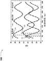
图1C展示了图表190,其是为不同颜色的光(蓝,绿,红)和抗反射涂层(ARC)的不同厚度而展示的光敏二极管量子效率(QE)的一个模拟例子。对于图表190中的模拟,该ARC包括位于氧化硅上方的氮化硅子层,其具表示氮化硅层厚度的x轴。如图表190所示,每种颜色的光电二极管 QE随氮化硅子层的厚度而变化,且单一子层的厚度不对应于所有颜色的最佳QE。如图1C所示,蓝光的QE在子层的厚度最大,约50nm(第一点 191附近),绿光的QE在子层的厚度最大,约60nm(第二点193附近),及红光的QE在子层的厚度最大,约80nm(第三点195附近)。因此,包含单一材料的单一子层厚度的ARC不一定对应于光的多种颜色的QE最大值,且对不同像素区的具有不同ARC属性的像素区与不同域可以提高图像传感器的QE。Figure 1C shows a
图2展示了在衬底111背侧115上第一颜色滤波器201、第二滤光器 203和第三滤光器205的形成,其分别位于第一ARC161、第二ARC171和第三ARC181上方。图2还展示了第一微透镜207、第二微透镜209和第三微透镜211的形成,其分别位于第一颜色滤波器201、第二滤光器203 和第三滤光器205。第一滤光器201、第二滤光器203和第三滤光器205可以各自都包括原色之一(例如,蓝色、绿色、红色)的单个过滤器,并且可以被定位,以过滤将射到第一光敏二极管119、第二光敏二极管121和第三光敏二极管123的光。第一滤光器201、第二滤光器203和第三滤光器205可以各自对应于第一ARC161、第二ARC171和第三ARC181的属性。例如,在第一像素区103中,第一滤光器201可以允许蓝光及第一 ARC161可以减少蓝光的反射。同样地,在第二像素区105中,第二滤光器203可以允许绿光及第二ARC171可以减少绿光的反射,且在第三像素区107,第三滤光器205可以准许红光及第三ARC181可以减少红光的反射。第一滤光器201、第二滤光器203和第三滤光器205可以是滤光器阵列图案的一部分。例如,第一滤光器201、第二滤光器203和第三滤光器 205可以是用于图像传感器100上方的滤光器位置上的拜耳RGB图案、 YotsubaCRGB图案的一部分。在一些实施例中,如图1A所示,第一滤光器201、第二滤光器203和第三滤光器205可以是滤光器阵列110的一部分。FIG. 2 shows the formation of a
一个或多个第一滤光器201、第二滤光器203和第三滤光器205可以包括聚合物材料或树脂,比如包括有色颜料的高分子聚合物。在实施例中,高分子聚合物被用于形成第一滤光器201、第二滤光器203和第三滤光器 205,每个第一滤光器201、第二滤光器203和第三滤光器205都可以通过使用比如旋涂的工艺形成于衬底111上方。在衬底111上方旋涂聚合材料之后,该材料可以通过使用合适的光刻掩模和蚀刻工艺被图案化以形成第一滤光器201、第二滤光器203和/或所述第三滤光器205。用于形成第一滤光器201、第二滤光器203和/或所述第三滤光器205的任何其它合适的方法也都可以被使用。One or more of the
第一微透镜207、第二微透镜209和第三微透镜211可以通过首次施加和图案化正性光刻胶(未示出)从而在第一滤光器201、第二滤光器203 和第三滤光器205上方形成。一旦形成,然后图案化的光刻胶可以被烘烤以使光刻胶进入第一微透镜207、第二微透镜209和第三微透镜211。第一微透镜207、第二微透镜209和第三微透镜211可以被用于更直接地聚焦入射光分别到第一光敏二极管119、第二光敏二极管121和第三光敏二极管123。The
图3展示包括第四ARC301和第五ARC303的示例性图像传感器的实施例。第四ARC301位于第一像素区103和第二像素区105上方,并包括位于第八子层307上方的第七子层305。第五ARC303位于第三像素区107 上方并包括第七子层305。FIG. 3 shows an embodiment of an exemplary image sensor including a
第四ARC301和第五ARC303通过在衬底111背侧115的上方形成第七子层305。如图3所述,第七子层305可以在第一像素区103、第二像素区105和第三像素区107的上方形成。第七介电层305的第七厚度t7在约


第八子层307可以在第七子层305上方形成。第八子层307可以形成在约


如图3的实施例所示,第一像素区103和第二像素区105通过第四 ARC301被覆盖,第四ARC301包括具有第七厚度t7的第七子层305和具有第八厚度t8的第八子层307。因此,第四ARC301的总厚度是第七厚度 t7和第八厚度t8.的总和。第三像素区107通过第五ARC303被覆盖,第五 ARC303包括第七子层305,并因此第五ARC303的总厚度是第七厚度t7。因此第一像素区103和第二像素区105都包括第四ARC301,其减少超过入射光波长的第一范围反射。第三像素区107包括第五ARC303而非第四 ARC301,第五ARC303具有不同的厚度,减少了入射光波长的不同范围的反射。例如,第四ARC301可以减少光的两种颜色(例如,蓝色和绿色、蓝色和红色,或绿色和红色)的反射及第五ARC303可以减少光的另一种颜色(例如,红色、绿色或蓝色)的反射。As shown in the embodiment of FIG. 3, the
在实施例中,可以形成附加第三子层(未示出)。附加第三子层可以在单个像素区(例如,位于第一像素区103、第二像素区105或第三像素区107上方)上方形成,或在多个像素区(例如,位于第一像素区103和第二像素区105上方,位于像素区的其它组合上方,或位于所有的像素区上方)上方形成。附加第三子层可以是与第七子层305和/或第八子层307相同的或不同的材料。在其他实施例中,第七子层305和/或第八子层307 可以是氧化硅,并且附加第三层可以是一种材料,比如氧化硅、氮化硅、碳化硅、氧化铝(Al2O3)、二氧化铪(HfO2)层、高k介电及其组合等。附加第三子层可以形成在约


在其它实施例中,也可以形成三个子层,并且位于像素区上方的ARC 可以包括三个以上的子层。以这种方式,不同的ARC可以为不同像素区的不同颜色的光进行优化。单个ARC可以为一个颜色以上的光进行优化,可以在一个以上的像素区的上方形成。In other embodiments, three sub-layers may also be formed, and the ARC above the pixel region may include more than three sub-layers. In this way, different ARCs can be optimized for different colors of light in different pixel regions. A single ARC can be optimized for more than one color of light and can be formed over more than one pixel area.
就先前图2所述的方式形成第四滤光器311、第五滤光器313和第六滤光器315及第一微透镜207、第二微透镜209和第三微透镜211。第四滤光器311的第九厚度t9,第五滤光器313的第十厚度t10和第六滤光器315 的第十一厚度t11可以都是相同的,或可以各自都具有在约300纳米至约 1000纳米之间的厚度。如图3所示的另一个实施例中,第九厚度9和第十厚度t10可以大约是600纳米,但是第十一厚度t11可以具有比大约700nm 更大的厚度。在其它实施例中,在第九厚度t9,、第十厚度和第十一厚度t11 的任何合适的组合可以具有相同或不同的厚度。The fourth
图4展示第六ARC401、第七ARC403和第八ARC405的实施例。在本实施例中,第六ARC401、第七ARC403和第八ARC405各自包括具有不同光学特性的不同材料。例如,第六ARC401、第七ARC403和第八 ARC405可以通过比如CVD、PECVD、热氧化或其组合的方法来形成,并且由一个或多个合适的介电材料,例如氧化硅、氮化硅、高k电介质及其组合等制成。例如,第六ARC401可以是氮化硅,第七ARC403可以是氧化硅及第八ARC405可以是高k电介质。其他材料和材料的组合也是可以的。FIG. 4 shows an embodiment of a
如图4所示,第六ARC401、第七ARC403和第八ARC405可以具有相同的厚度,尽管在其他实施例中,一个或多个第六ARC401、第七ARC403 和第八ARC405可以具有不同的厚度。例如,第六ARC401、第七ARC403 和第八ARC405可以具有在约


第六ARC401、第七ARC403和第八弧405可以用合适的沉积和光刻掩模及蚀刻工艺分别在第一像素区103、第二像素区105和第三像素区107 的上方形成。例如,第六ARC401可以通过使用光刻和蚀刻技术在衬底111 上方沉积材料,然后图案化该材料以形成位于第一像素区103上方的第六 ARC401来形成。接着,第二材料可以被沉积并图案化,以形成位于第二像素区105上方的第七ARC403,然后第三材料可以被沉积并图案化,以形成位于第三像素区107上方的第八ARC405。The
在一些实施例中,特定的材料层可以在一个以上的像素区上方形成。例如,可以形成和图案化第一材料,以形成位于第一像素区103和第二像素区105上方的单个ARC。接着,可以形成和图案化第二材料,以形成位于第三像素区107上方的ARC。在一些实施例中,一个或多个第六ARC401、第七ARC403和第八ARC405可以包括相同或不同材料的多个子层。这些都是例子;在不同像素区上方形成具有不同材料的ARC的其它结构是可以的。In some embodiments, a particular material layer may be formed over more than one pixel region. For example, the first material can be formed and patterned to form a single ARC over the
由于具有不同的光学特性,每个第六ARC401、第七ARC403和第八 ARC405都可以减少不同颜色入射光的反射。例如,三个不同的材料可以被分别选择为第六ARC401、第七ARC403和第八ARC405,以分别减少蓝光、绿光和红光的反射。第六ARC401、第七ARC403和第八ARC405各自都可以具有在约1.4至约5之间的不同折射索引。例如,第六ARC401、第七ARC403和第八ARC405各自都可以具有
在一些实施例中,第六ARC401、第七ARC403和第八ARC405可以包括提供具有不同光学特性的不同组合物的相同材料。在本实施例中,不同的光学特性可以通过使用不同的形成条件,比如流速(例如前体流速)、掺杂浓度、温度、压力或其他条件来实现。第六ARC401、第七ARC403 和第八ARC405可以包括具有不同的物理性质,诸如掺杂浓度、掺杂剂类型、缺陷型或密度、错配型或浓度或其它性质的相同的材料。In some embodiments, the
在一些实施例中,第六ARC401、第七ARC403和第八ARC405可以各自包括相同的材料,但是在第六ARC401、第七ARC403和第八ARC405 各自的形成过程中,前体流速可以是不同的,从而第六ARC401、第七 ARC403和第八ARC405具有不同的折射率。例如,第六ARC401、第七 ARC403和第八ARC405可以各自都是氮化硅,但是每个前体流速可以是不同的,以形成具有不同折射率的氮化硅。例如,使用硅烷(SiH4)作为第一前体,氮气(N2)作为第二前体,氨(NH3)作为第三前体可以形成氮化硅,及使用在40sccm至300sccm之间,比如约110sccm的第一前体流速,在2000sccm至20000sccm之间,比如8000sccm的第二前体流速,在 20sccm至300sccm之间,比如80sccm的第三前体流速可以形成第六 ARC401,因此第六ARC401将有1.9的第一折射率。In some embodiments, the
使用在40sccm至300sccm之间,比如约90sccm的第一前体流速,在 2000sccm至20000sccm之间,比如7000sccm的第二前体流速,在20sccm 至300sccm之间,比如60sccm的第三前体流速可以形成第七ARC403的氮化硅,因此第六ARC403将有2.0的第一折射率。使用在40sccm至300sccm 之间,比如约60sccm的第一前体流速,在2000sccm至20000sccm之间,比如5000sccm的第二前体流速,在20sccm至300sccm之间,比如30sccm 的第三前体流速可以形成第七ARC405的氮化硅,因此第六ARC405将有 2.1的第一折射率。Using a first precursor flow rate between 40 sccm and 300 sccm, such as about 90 sccm, a second precursor flow rate between 2000 sccm and 20000 sccm, such as 7000 sccm, a third precursor flow rate between 20 sccm and 300 sccm, such as 60 sccm may The silicon nitride forming the
在一些实施例中,第六ARC401、第七ARC403和第八ARC405可以各自包括相同的材料,但是在第六ARC401、第七ARC403和第八ARC405 各自的形成过程中,前体流速可以是不同的,从而第六ARC401、第七 ARC403和第八ARC405具有不同的折射率。例如,第六ARC401、第七 ARC403和第八ARC405可以各自都是氮化硅,但是每个形成压力可以是不同的,以形成具有不同折射率的氮化硅。例如,用1托的压力可以形成具有1.9的第一折射率的第六ARC401,用5托的压力可以形成具有2.0的第一折射率的第七ARC403,用20托的压力可以形成具有2.1的第一折射率的第八ARC405。In some embodiments, the
在一些实施例中,第六ARC401、第七ARC403和第八ARC405可以各自包括相同的材料,但是在第六ARC401、第七ARC403和第八ARC405 各自的形成过程中,形成温度可以是不同的,从而第六ARC401、第七 ARC403和第八ARC405具有不同的折射率。例如,第六ARC401、第七 ARC403和第八ARC405可以各自都是氮化硅,但是每个形成压力可以是不同的,以形成具有不同折射率的氮化硅。例如,用250oC的温度可以形成具有1.9的第一折射率的第六ARC401,用350oC的温度可以形成具有 2.0的第一折射率的第七ARC403,用405oC的温度可以形成具有2.1的第一折射率的第八ARC405。In some embodiments, the
在一些实施例中,第六ARC401、第七ARC403和第八ARC405可以各自包括相同的材料,但是在第六ARC401、第七ARC403和第八ARC405 各自的形成过程中,形成温度可以是不同的,从而第六ARC401、第七 ARC403和第八ARC405具有不同的折射率。例如,第六ARC401、第七 ARC403和第八ARC405可以各自都是掺氢的氮化硅,但是可以具有不同的掺杂浓度,以具有不同的折射率。例如,用1E20/cm3的掺杂浓度可以形成具有1.9的第一折射率的第六ARC401,用5E20/cm3的掺杂浓度可以形成具有2.0的第一折射率的第七ARC403,用1E21/cm3的掺杂浓度可以形成具有2.1的第一折射率的第八ARC405。In some embodiments, the
图5展示了图表500,其显示了光敏二极管量子效率(EQE)的示例。第一曲线501通过蓝色滤光器和仅用于蓝光且其厚度被选择以最大化QE 的单一ARC,示出了光敏二极管的QE。第二曲线503通过蓝色滤光器和用于蓝光、绿光和红光且其厚度被选择以最大化QE的单一ARC,示出了光敏二极管的QE。如图表 500所示,可以通过使用用于特定颜色光,而非为多种颜色光的ARC来提高QE。FIG. 5 illustrates a
图6A-B展示了第一像素阵列600和第二像素阵列650的实施例。第一像素阵列600和第二像素阵列650可以是像素传感器,比如像素传感器100 的一部分。例如,第一像素阵列600和第二像素阵列650可以是图1A中所示的像素阵列110的一部分。第一像素阵列600包含多个像素区,如图6A 所示的第一绿色像素区601、第一蓝色像素区603和第一红色像素区605。第一绿色像素区601、第一蓝色像素区603和第一红色像素区605可以类似于图1A中讨论所述的第一像素区103、第二像素区105和/或第三像素区107。在本实施例中,第一绿色像素区601与绿光相关联。例如,第一绿色像素区601可以具有绿色滤光器和为绿光设计的ARC。同样地,第一蓝色像素区603与蓝光相关联及第一红色像素区605与红光相关联。第一绿色像素区601、第一蓝色像素区603和第一红色像素区605可以被布置在拜耳RGB图案、YotsubaCRGB图案或任何其它合适的图案中。6A-B illustrate embodiments of a
图6A展示了一个实施例,其中第一绿色像素区601具有比第一蓝色像素区603或第一红色像素区605更大的区域。例如,第一绿色像素区601 可以具有第一宽度w1及第一蓝色像素区603和第一红色像素区605可以各自具有相同的第二宽度w2。如图6A所示,第一绿色像素区601可以具有比第一蓝色像素区603和第一红色像素区605的对应第二宽度w2更长的第一宽度w1。例如,第一宽度w1可以比第二宽度w2长约1%、5%、10%、 100%或其它长度。例如,第二宽度w2可以在约0.8微米至约1.05微米之间,比如约1微米,及第一宽度w1可以在约1微米至约1.3微米之间,比如约1.1微米。在一个实施例中,第一绿色像素区601的面积可以在1μm2 至1.69μm2之间,比如约1.21μm2,及第一蓝色像素区603和第一红色像素区605的面积可以在0.64μm2至1.1025μm2之间,例如约1μm2。在一些情况下,第一绿色像素区601的较大面积允许第一绿色像素区601接收比第一蓝色像素区603或第一红色像素区605更多的照明。FIG. 6A shows an embodiment in which the first
在一些实施例中,第一绿色像素区601可以包括或由具有与第一蓝色像素区603或第一红色像素区605不同的宽度、面积或形状的一个或多个注入物来限定。第一绿色像素区601的注入物也可以具有与第一蓝色像素区603或第一红色像素区605不同的浓度、注入离子、掺杂分布、退火温度或其它不同的特性。在其它实施例中,像素区可以具有其它宽度或面积。例如,第一绿色像素区601可以具有与第一蓝色像素区603不同的宽度或面积,及第一蓝色像素区603可以具有与第一红色像素区605不同的宽度或面积。In some embodiments, the first
图6B展示了第二像素阵列650的实施例,其包含第二绿色像素区651、第二蓝色像素区653和第二红色像素区655。如图6B所示,第二绿色像素区651具有与第二蓝色像素区653或第二红色像素区655不同的形状。第二绿色像素区651具有八边形形状及第二蓝色像素区653和第二红色像素区655具有正方形形状。在一些情况下,第二绿色像素区651的八边形形状允许第二绿色像素区651的相对大小更大并由此接收比第二蓝色像素区 653或第二红色像素区655更多的照明。在一些实施例中,第二绿色像素区651可以包括或由具有与第二蓝色像素区653或第二红色像素区655不同的宽度、面积或形状的一个或多个注入物来限定。第二绿色像素区651 的注入物也可以具有与第二蓝色像素区653或第二红色像素区655不同的浓度、注入离子、掺杂分布、退火温度或其它不同的特性。在其它实施例中,像素区可以具有其它形状或以其它图案被布置。例如,像素区可以是方形、矩形、八边形、多边形、不规则形状或其它形状,并具有直链或圆角。FIG. 6B shows an embodiment of the
在一些实施例中,每种类型像素区都可以具有不同的形状。例如,第二绿色像素区651可以具有八边形形状,第二蓝色像素区653可以具有正方形形状,及第二红色像素区655可以具有矩形形状。在一些实施例中,单一类型的像素区可以具有不止一种形状。例如,像素阵列中的绿色像素区可以是第一尺寸的八边形,及相同像素阵列中的另一个绿色像素区可以是第二尺寸的八边形。又例如,像素阵列中的绿色像素区可以是正方形,及同一像素阵列中的另一个绿色像素区可以是矩形。In some embodiments, each type of pixel region may have a different shape. For example, the second
通过增加绿色像素区(例如,第一绿色像素区601或第二绿色像素区 651)的相对大小,入射照明的更大部分入射到绿色像素区并因此绿色像素区接收的照明可以会增加。在一些情况下,由图像传感器接收的照明可以具有靠近绿色的峰值强度,并因此绿色像素区相对面积的增加可以导致图像传感器量子效率的增加或信噪比(SNR)的增加。增加绿色像素区的相对大小也可以允许图像传感器中不同像素区上方分散更多的有效能量,其中光的能量E(eV)波长

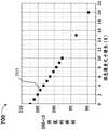
图7展示了示例性图表700,其显示了增加的绿色像素区可以允许更大的信噪比(SNR)。对于给定的相对绿色像素区大小,数据点701显示照明功率(任意单位)以产生SNR=10。在图表700中,所给的绿色像素大小是作为关于红色和蓝色像素区的绿色像素区宽度的增加百分比的。如图7所示,增加绿色像素区的相对大小可以增加达到所给SNR的照明。FIG. 7 illustrates an
在一些实施例中,图6A-B所示的一个或多个像素区可以包含图1B和图2-4所示的一个或多个ARC。例如,第一绿色像素区601或第二绿色像素区651可以包含被配置为减少绿光反射的ARC。同样,第一蓝色像素区 603或第二蓝色像素区653可以包含被配置为减少蓝光反射的ARC,及第一红色像素区605或第二红色像素区655可以包含被配置为减少红光反射的ARC。例如,第一绿色像素区601可以包含第二ARC171,第一蓝色像素区603可以包含第一ARC161,及第一红色像素区605可以包含第三 ARC181。这是一个例子;可以使用像素区和ARC的其它配置和组合。在一些实施例中,图像传感器是一个前端发光的图像传感器。In some embodiments, one or more of the pixel regions shown in Figures 6A-B may contain one or more of the ARCs shown in Figures 1B and 2-4. For example, the first
通过在不同的像素区上形成不同的ARC,可以会提高图像传感器整体的量子效率和/或信噪比。在某些情况下,使用不同像素区的不同AEC可以减少像素区之间的串扰,每个像素区可被配置或优化为不同颜色的光。为特定颜色的光而配置的像素区可以由于不需要的颜色的光入射至光电二极管而有大量减少的噪声。因为每个像素区可以包含为特定颜色的光而配置的ARC,位于像素区上方的每个滤光器的厚度可以会降低。较薄的彩色滤光片可以允许减少图像传感器的总厚度。By forming different ARCs on different pixel regions, the overall quantum efficiency and/or signal-to-noise ratio of the image sensor can be improved. In some cases, crosstalk between pixel regions can be reduced by using different AECs for different pixel regions, each of which can be configured or optimized for a different color of light. Pixel regions configured for light of a particular color may have substantially reduced noise due to light of an undesired color incident on the photodiode. Since each pixel region may contain an ARC configured for a specific color of light, the thickness of each filter located above the pixel region may be reduced. Thinner color filters can allow for a reduction in the overall thickness of the image sensor.
根据实施例,一种半导体器件,其包含包括第一像素区和在衬底上的第二像素区的图像传感器,第一像素区接近第二像素区。第一抗反射涂层,其位于第一像素区的上方,所述第一抗反射涂层为第一波长范围的入射光减少反射;第二抗反射涂层,其位于第二像素区的上方,所述第二抗反射涂层为第二波长范围的入射光减少反射,所述第二波长范围不同于所述第一波长范围。According to an embodiment, a semiconductor device includes an image sensor including a first pixel region and a second pixel region on a substrate, the first pixel region being close to the second pixel region. The first anti-reflection coating, which is located above the first pixel area, and the first anti-reflection coating reduces the reflection of incident light in the first wavelength range; the second anti-reflection coating, which is located above the second pixel area , the second anti-reflection coating reduces reflection of incident light in a second wavelength range, the second wavelength range being different from the first wavelength range.
根据另一个实施例,半导体器件包含衬底、在该衬底第一像素区中的第一光敏二极管,及在该衬底第二像素区中的第二光敏二极管。第一次像素区具有与第二个像素区不同的尺寸。According to another embodiment, a semiconductor device includes a substrate, a first photodiode in a first pixel region of the substrate, and a second photodiode in a second pixel region of the substrate. The first pixel area has a different size from the second pixel area.
根据另一个实施例,制造图像传感器器件的方法包含在衬底的第一区中注入离子以形成第一光敏二极管及在衬底的第二区中注入离子以形成第二光敏二极管,其中,第一区接近第二区。第一材料的第一层沉积于第一区上方,其中,第一层为第一抗反射涂层。第二材料的第二层沉积于第二区上方,其中,第一层为第一抗反射涂层且第二层不同于第一层。According to another embodiment, a method of manufacturing an image sensor device includes implanting ions in a first region of a substrate to form a first photodiode and implanting ions in a second region of the substrate to form a second photodiode, wherein the first District one is close to district two. A first layer of a first material is deposited over the first region, wherein the first layer is a first anti-reflective coating. A second layer of a second material is deposited over the second region, wherein the first layer is the first anti-reflective coating and the second layer is different from the first layer.
根据本发明的一个方面,提供一种半导体器件,包括:图像传感器,包括在衬底中的第一像素区和第二像素区,第一像素区邻近第二像素区;第一抗反射涂层,位于第一像素区的上方,第一抗反射涂层为第一波长范围的入射光减少反射;以及第二抗反射涂层,位于第二像素区的上方,第二抗反射涂层为第二波长范围的入射光减少反射,第二波长范围不同于第一波长范围。According to one aspect of the present invention, a semiconductor device is provided, comprising: an image sensor including a first pixel region and a second pixel region in a substrate, the first pixel region adjacent to the second pixel region; a first anti-reflection coating , located above the first pixel area, the first anti-reflection coating reduces reflection of incident light in the first wavelength range; and the second anti-reflection coating, located above the second pixel area, the second anti-reflection coating is the second anti-reflection coating Reflection is reduced for incident light in two wavelength ranges, the second wavelength range being different from the first wavelength range.
根据本发明的一个实施例,第一抗反射涂层包括第一子层和形成在第一子层上方的第二子层,第二抗反射涂层包括第三子层和形成在第三子层上方的第四子层。According to one embodiment of the present invention, the first antireflection coating includes a first sublayer and a second sublayer formed above the first sublayer, and the second antireflection coating includes a third sublayer and a second sublayer formed on the third sublayer. The fourth sublayer above the layer.
根据本发明的一个实施例,第一子层的厚度不同于第三子层的厚度,并且第二子层的厚度不同于第四子层的厚度。According to one embodiment of the invention, the thickness of the first sublayer is different from the thickness of the third sublayer, and the thickness of the second sublayer is different from the thickness of the fourth sublayer.
根据本发明的一个实施例,第一子层包含与第二子层不同的材料。According to one embodiment of the invention, the first sublayer comprises a different material than the second sublayer.
根据本发明的一个实施例,第一子层包含与第二子层相同的材料。According to one embodiment of the invention, the first sublayer comprises the same material as the second sublayer.
根据本发明的一个实施例,第一抗反射涂层的厚度不同于第二抗反射涂层的厚度。According to one embodiment of the invention, the thickness of the first antireflection coating is different from the thickness of the second antireflection coating.
根据本发明的一个实施例,第一抗反射涂层包括氮化硅。According to one embodiment of the invention, the first anti-reflection coating comprises silicon nitride.
根据本发明的一个实施例,第一像素区具有比第二像素区更大的面积。According to an embodiment of the present invention, the first pixel area has a larger area than the second pixel area.
根据本发明的另一方面,提供一种半导体器件,包括:衬底;位于衬底的第一像素区中的第一光敏二极管;以及位于衬底的第二像素区中的第二光敏二极管,其中,第一像素区与第二像素区具有不同的尺寸。According to another aspect of the present invention, a semiconductor device is provided, comprising: a substrate; a first photodiode located in a first pixel region of the substrate; and a second photodiode located in a second pixel region of the substrate, Wherein, the first pixel area and the second pixel area have different sizes.
根据本发明的一个实施例,第一像素区具有在约1.0微米至1.3微米之间的第一尺寸,并且第二像素区具有在约0.8微米至1.05微米之间的第二尺寸,第一尺寸大于第二尺寸。According to one embodiment of the present invention, the first pixel area has a first size between about 1.0 micron and 1.3 micron, and the second pixel area has a second size between about 0.8 micron and 1.05 micron, the first size larger than the second dimension.
根据本发明的一个实施例,第一像素区具有比第二像素区更大的面积。According to an embodiment of the present invention, the first pixel area has a larger area than the second pixel area.
根据本发明的一个实施例,第一像素区具有比第二像素区的面积大约 5%至约100%的第一面积。According to one embodiment of the present invention, the first pixel region has a first area that is about 5% to about 100% larger than that of the second pixel region.
根据本发明的一个实施例,第一像素区包括第一抗反射涂层,并且第二像素区包括第二抗反射涂层,第二抗反射涂层与第一抗反射涂层不同。According to an embodiment of the present invention, the first pixel area includes a first anti-reflection coating, and the second pixel area includes a second anti-reflection coating, the second anti-reflection coating being different from the first anti-reflection coating.
根据本发明的一个实施例,第一像素区包括第一注入区并且第二像素区包括第二注入区,第二注入区与第一注入区不同。According to an embodiment of the present invention, the first pixel region includes a first implantation region and the second pixel region includes a second implantation region, the second implantation region being different from the first implantation region.
根据本发明的一个实施例,第一注入区具有与第二注入区不同的尺寸。According to one embodiment of the invention, the first implanted region has a different size than the second implanted region.
根据本发明的一个实施例,第一像素区具有与第二像素区不同的形状。According to an embodiment of the present invention, the first pixel area has a different shape from the second pixel area.
根据本发明的一个实施例,第一像素区具有八边形形状并且第二像素区具有正方形形状。According to one embodiment of the present invention, the first pixel area has an octagonal shape and the second pixel area has a square shape.
根据本发明的另一方面,提供一种制造图像传感器器件的方法,方法包括:在衬底的第一区中注入离子以形成第一光敏二极管;在衬底的第二区中注入离子以形成第二光敏二极管,其中,第一区邻近第二区;在第一区的上方沉积第一材料的第一层,其中,第一层为第一抗反射涂层;以及在第二区的上方沉积第二材料的第二层,其中,第二层为第二抗反射涂层,并且第二层与第一层不同。According to another aspect of the present invention, there is provided a method of manufacturing an image sensor device, the method comprising: implanting ions in a first region of a substrate to form a first photodiode; implanting ions in a second region of a substrate to form a second photodiode, wherein the first region is adjacent to the second region; a first layer of a first material is deposited over the first region, wherein the first layer is a first anti-reflective coating; and over the second region A second layer of a second material is deposited, wherein the second layer is a second anti-reflective coating, and the second layer is different from the first layer.
根据本发明的一个实施例,沉积第一层包括:沉积第一子层;以及在第一层上方沉积第二层。According to an embodiment of the present invention, depositing the first layer includes: depositing a first sub-layer; and depositing a second layer over the first layer.
根据本发明的一个实施例,第二材料与第一材料不同。According to one embodiment of the invention, the second material is different from the first material.
前述内容概述了多个实施例的特征,从而使得本领域的技术人员能较好地理解本公开的方面。本领域的技术人员应理解,其可以轻松地将本公开作为基础,用于设计或修改其他工艺或结构,从而达成与本文所介绍实施例的相同目的和/或实现相同的优点。本领域技术人员还应认识到,这种等效结构并不背离本公开的精神和范围,并且其可以进行各种更改、替换和变更而不背离本公开的精神和范围。The foregoing summary summarizes features of various embodiments so that those skilled in the art can better understand aspects of the disclosure. Those skilled in the art should understand that they can easily use this disclosure as a basis for designing or modifying other processes or structures, so as to achieve the same purpose and/or achieve the same advantages as the embodiments presented herein. Those skilled in the art should also realize that such equivalent constructions do not depart from the spirit and scope of the present disclosure, and that they may make various changes, substitutions and alterations without departing from the spirit and scope of the present disclosure.
Claims (41)
Translated fromChineseApplications Claiming Priority (2)
| Application Number | Priority Date | Filing Date | Title |
|---|---|---|---|
| US14/996,462 | 2016-01-15 | ||
| US14/996,462US9673239B1 (en) | 2016-01-15 | 2016-01-15 | Image sensor device and method |
Publications (2)
| Publication Number | Publication Date |
|---|---|
| CN107342300A CN107342300A (en) | 2017-11-10 |
| CN107342300Btrue CN107342300B (en) | 2022-11-11 |
Family
ID=58778617
Family Applications (1)
| Application Number | Title | Priority Date | Filing Date |
|---|---|---|---|
| CN201611155540.2AActiveCN107342300B (en) | 2016-01-15 | 2016-12-14 | Semiconductor device and method of manufacturing image sensor device |
Country Status (3)
| Country | Link |
|---|---|
| US (4) | US9673239B1 (en) |
| CN (1) | CN107342300B (en) |
| TW (1) | TWI709760B (en) |
Families Citing this family (17)
| Publication number | Priority date | Publication date | Assignee | Title |
|---|---|---|---|---|
| CN110073493A (en)* | 2016-12-27 | 2019-07-30 | 凸版印刷株式会社 | Solid-state image pickup element and its manufacturing method |
| CN109711230B (en)* | 2017-10-26 | 2023-05-02 | 中芯国际集成电路制造(上海)有限公司 | Semiconductor fingerprint sensor, manufacturing method thereof and electronic device |
| EP3707755B1 (en)* | 2018-02-12 | 2024-04-03 | TriEye Ltd. | Germanium on insulator for cmos imagers in the short wave infrared |
| KR102531355B1 (en)* | 2018-03-20 | 2023-05-10 | 삼성전자주식회사 | image sensor |
| KR20190124963A (en)* | 2018-04-27 | 2019-11-06 | 주식회사 디비하이텍 | Backside illuminated image sensor and method of manufacturing the same |
| US10854647B2 (en) | 2018-11-30 | 2020-12-01 | Taiwan Semiconductor Manufacturing Co., Ltd. | Photo diode with dual backside deep trench isolation depth |
| CN109742108B (en)* | 2019-01-03 | 2020-12-01 | 京东方科技集团股份有限公司 | A display panel, its manufacturing method, and display device |
| WO2020204833A1 (en)* | 2019-04-01 | 2020-10-08 | Meridian Innovation Pte Ltd | Monolithic post complementary metal-oxide-semiconductor integration of thermoelectric-based infrared detector |
| US11721774B2 (en)* | 2020-02-27 | 2023-08-08 | Taiwan Semiconductor Manufacturing Company, Ltd. | Full well capacity for image sensor |
| CN113314551A (en) | 2020-02-27 | 2021-08-27 | 台湾积体电路制造股份有限公司 | Image sensor and forming method thereof |
| TWI740512B (en)* | 2020-05-26 | 2021-09-21 | 睿生光電股份有限公司 | X-ray device |
| KR102852530B1 (en)* | 2020-08-12 | 2025-09-02 | 삼성디스플레이 주식회사 | Display device |
| CN114388537A (en)* | 2020-10-21 | 2022-04-22 | 中芯国际集成电路制造(北京)有限公司 | Image sensor and method of forming the same |
| CN114864610A (en)* | 2021-01-20 | 2022-08-05 | 中芯国际集成电路制造(北京)有限公司 | Image sensor and forming method thereof |
| US20230009280A1 (en)* | 2021-07-06 | 2023-01-12 | Samsung Electronics Co., Ltd. | Image sensor |
| US20240145498A1 (en)* | 2022-10-26 | 2024-05-02 | Taiwan Semiconductor Manufacturing Company, Ltd. | Substrate contact in wafer backside |
| JP2025030261A (en)* | 2023-08-23 | 2025-03-07 | ソニーセミコンダクタソリューションズ株式会社 | Photodetection devices and electronic equipment |
Citations (3)
| Publication number | Priority date | Publication date | Assignee | Title |
|---|---|---|---|---|
| CN102074563A (en)* | 2008-10-10 | 2011-05-25 | 台湾积体电路制造股份有限公司 | Image sensor having enhanced backside illumination quantum efficiency |
| CN103227178A (en)* | 2012-01-31 | 2013-07-31 | 台湾积体电路制造股份有限公司 | Methods and apparatus for an improved reflectivity optical grid for image sensors |
| CN103378112A (en)* | 2012-04-26 | 2013-10-30 | 台湾积体电路制造股份有限公司 | Image sensor device and method |
Family Cites Families (27)
| Publication number | Priority date | Publication date | Assignee | Title |
|---|---|---|---|---|
| JPH04199876A (en)* | 1990-11-29 | 1992-07-21 | Nec Corp | Solid state image sensing device and manufacture thereof |
| US7759679B2 (en)* | 2004-01-15 | 2010-07-20 | Panasonic Corporation | Solid-state imaging device, manufacturing method of solid-state imaging device, and camera employing same |
| EP1816677A1 (en)* | 2004-09-09 | 2007-08-08 | Matsushita Electric Industrial Co., Ltd. | Solid-state image pickup element |
| KR100719341B1 (en)* | 2005-01-25 | 2007-05-17 | 삼성전자주식회사 | Image sensor and its manufacturing method |
| JP4224036B2 (en)* | 2005-03-17 | 2009-02-12 | 富士通マイクロエレクトロニクス株式会社 | Image sensor with embedded photodiode region and method of manufacturing the same |
| JP2007025009A (en)* | 2005-07-13 | 2007-02-01 | Kyocera Mita Corp | Optical scanner unit and image forming apparatus equipped therewith |
| US7829908B2 (en)* | 2005-11-11 | 2010-11-09 | Nikon Corporation | Solid-state image sensors and display devices having anti-reflection film |
| US20070131988A1 (en)* | 2005-12-12 | 2007-06-14 | Taiwan Semiconductor Manufacturing Co., Ltd. | CMOS image sensor devices and fabrication method thereof |
| US20090302409A1 (en)* | 2008-06-04 | 2009-12-10 | Omnivision Technologies, Inc. | Image sensor with multiple thickness anti-relfective coating layers |
| KR20100012677A (en)* | 2008-07-29 | 2010-02-08 | 주식회사 동부하이텍 | Image sensor and method of manufacturing the same |
| US8334195B2 (en)* | 2009-09-09 | 2012-12-18 | International Business Machines Corporation | Pixel sensors of multiple pixel size and methods of implant dose control |
| KR101647779B1 (en)* | 2009-09-09 | 2016-08-11 | 삼성전자 주식회사 | Image sensor, fabricating method thereof, and device comprising the image sensor |
| JP2011100900A (en)* | 2009-11-06 | 2011-05-19 | Sony Corp | Solid-state imaging apparatus and method of manufacturing and method of designing the same, and electronic apparatus |
| JP2011129723A (en)* | 2009-12-17 | 2011-06-30 | Sharp Corp | Method of manufacturing solid-state imaging device |
| WO2011156507A1 (en)* | 2010-06-08 | 2011-12-15 | Edward Hartley Sargent | Stable, sensitive photodetectors and image sensors including circuits, processes, and materials for enhanced imaging performance |
| JP2012038938A (en)* | 2010-08-06 | 2012-02-23 | Canon Inc | Solid state image sensor and camera |
| JP5659759B2 (en)* | 2010-12-10 | 2015-01-28 | セイコーエプソン株式会社 | Solid-state imaging device |
| TWI577001B (en)* | 2011-10-04 | 2017-04-01 | Sony Corp | Solid-state imaging device, method of manufacturing solid-state imaging device, and electronic device |
| JP2013131553A (en)* | 2011-12-20 | 2013-07-04 | Toshiba Corp | Solid-state imaging device |
| US8779484B2 (en)* | 2012-11-29 | 2014-07-15 | United Microelectronics Corp. | Image sensor and process thereof |
| US9691809B2 (en)* | 2013-03-14 | 2017-06-27 | Taiwan Semiconductor Manufacturing Company, Ltd. | Backside illuminated image sensor device having an oxide film and method of forming an oxide film of a backside illuminated image sensor device |
| KR102066603B1 (en)* | 2013-07-03 | 2020-01-15 | 에스케이하이닉스 주식회사 | Image sensor having the 3d photoelectric conversion device |
| JP2015065270A (en)* | 2013-09-25 | 2015-04-09 | ソニー株式会社 | Solid state image pickup device and manufacturing method of the same, and electronic apparatus |
| JP6115787B2 (en)* | 2013-12-18 | 2017-04-19 | ソニー株式会社 | Solid-state imaging device, manufacturing method thereof, and electronic apparatus |
| KR102240020B1 (en)* | 2014-08-29 | 2021-04-14 | 삼성전자주식회사 | Electronic device having a color filter |
| TW201628179A (en)* | 2015-01-21 | 2016-08-01 | Jsr 股份有限公司 | Solid-state imaging device and infrared absorbing composition |
| JP6671864B2 (en)* | 2015-05-18 | 2020-03-25 | キヤノン株式会社 | Imaging device manufacturing method and imaging device |
- 2016
- 2016-01-15USUS14/996,462patent/US9673239B1/enactiveActive
- 2016-11-11TWTW105136945Apatent/TWI709760B/enactive
- 2016-12-14CNCN201611155540.2Apatent/CN107342300B/enactiveActive
- 2017
- 2017-05-31USUS15/610,034patent/US10748948B2/enactiveActive
- 2019
- 2019-09-12USUS16/568,586patent/US11201183B2/enactiveActive
- 2021
- 2021-12-13USUS17/549,501patent/US11855109B2/enactiveActive
Patent Citations (3)
| Publication number | Priority date | Publication date | Assignee | Title |
|---|---|---|---|---|
| CN102074563A (en)* | 2008-10-10 | 2011-05-25 | 台湾积体电路制造股份有限公司 | Image sensor having enhanced backside illumination quantum efficiency |
| CN103227178A (en)* | 2012-01-31 | 2013-07-31 | 台湾积体电路制造股份有限公司 | Methods and apparatus for an improved reflectivity optical grid for image sensors |
| CN103378112A (en)* | 2012-04-26 | 2013-10-30 | 台湾积体电路制造股份有限公司 | Image sensor device and method |
Also Published As
| Publication number | Publication date |
|---|---|
| TWI709760B (en) | 2020-11-11 |
| US20200006408A1 (en) | 2020-01-02 |
| CN107342300A (en) | 2017-11-10 |
| US10748948B2 (en) | 2020-08-18 |
| US11201183B2 (en) | 2021-12-14 |
| US20170263657A1 (en) | 2017-09-14 |
| US11855109B2 (en) | 2023-12-26 |
| TW201727269A (en) | 2017-08-01 |
| US20220102396A1 (en) | 2022-03-31 |
| US9673239B1 (en) | 2017-06-06 |
Similar Documents
| Publication | Publication Date | Title |
|---|---|---|
| CN107342300B (en) | Semiconductor device and method of manufacturing image sensor device | |
| US10062728B2 (en) | Image sensor device and method | |
| US11158662B2 (en) | Semiconductor image sensor | |
| CN102074563B (en) | Image sensor having enhanced backside illumination quantum efficiency | |
| US9613996B2 (en) | Backside structure and methods for BSI image sensors | |
| CN104600084A (en) | Image Sensor Comprising Reflective Guide Layer and Method of Forming the Same | |
| US20210351225A1 (en) | Image sensor grid and method of manufacturing same | |
| US9601535B2 (en) | Semiconducator image sensor having color filters formed over a high-K dielectric grid | |
| US9356060B2 (en) | Image sensor device and method | |
| TW202238975A (en) | Transfer finfet | |
| US8860101B2 (en) | Image sensor cross-talk reduction system | |
| KR102616543B1 (en) | Light blocking layer for image sensor device |
Legal Events
| Date | Code | Title | Description |
|---|---|---|---|
| PB01 | Publication | ||
| PB01 | Publication | ||
| SE01 | Entry into force of request for substantive examination | ||
| SE01 | Entry into force of request for substantive examination | ||
| GR01 | Patent grant | ||
| GR01 | Patent grant |