CN107342216B - Plasma Activated Conformal Dielectric Film Deposition - Google Patents
Plasma Activated Conformal Dielectric Film DepositionDownload PDFInfo
- Publication number
- CN107342216B CN107342216BCN201710347032.2ACN201710347032ACN107342216BCN 107342216 BCN107342216 BCN 107342216BCN 201710347032 ACN201710347032 ACN 201710347032ACN 107342216 BCN107342216 BCN 107342216B
- Authority
- CN
- China
- Prior art keywords
- reactant
- film
- plasma
- cfd
- dopant
- Prior art date
- Legal status (The legal status is an assumption and is not a legal conclusion. Google has not performed a legal analysis and makes no representation as to the accuracy of the status listed.)
- Active
Links
Images


Classifications
- C—CHEMISTRY; METALLURGY
- C23—COATING METALLIC MATERIAL; COATING MATERIAL WITH METALLIC MATERIAL; CHEMICAL SURFACE TREATMENT; DIFFUSION TREATMENT OF METALLIC MATERIAL; COATING BY VACUUM EVAPORATION, BY SPUTTERING, BY ION IMPLANTATION OR BY CHEMICAL VAPOUR DEPOSITION, IN GENERAL; INHIBITING CORROSION OF METALLIC MATERIAL OR INCRUSTATION IN GENERAL
- C23C—COATING METALLIC MATERIAL; COATING MATERIAL WITH METALLIC MATERIAL; SURFACE TREATMENT OF METALLIC MATERIAL BY DIFFUSION INTO THE SURFACE, BY CHEMICAL CONVERSION OR SUBSTITUTION; COATING BY VACUUM EVAPORATION, BY SPUTTERING, BY ION IMPLANTATION OR BY CHEMICAL VAPOUR DEPOSITION, IN GENERAL
- C23C16/00—Chemical coating by decomposition of gaseous compounds, without leaving reaction products of surface material in the coating, i.e. chemical vapour deposition [CVD] processes
- C23C16/04—Coating on selected surface areas, e.g. using masks
- C23C16/045—Coating cavities or hollow spaces, e.g. interior of tubes; Infiltration of porous substrates
- C—CHEMISTRY; METALLURGY
- C23—COATING METALLIC MATERIAL; COATING MATERIAL WITH METALLIC MATERIAL; CHEMICAL SURFACE TREATMENT; DIFFUSION TREATMENT OF METALLIC MATERIAL; COATING BY VACUUM EVAPORATION, BY SPUTTERING, BY ION IMPLANTATION OR BY CHEMICAL VAPOUR DEPOSITION, IN GENERAL; INHIBITING CORROSION OF METALLIC MATERIAL OR INCRUSTATION IN GENERAL
- C23C—COATING METALLIC MATERIAL; COATING MATERIAL WITH METALLIC MATERIAL; SURFACE TREATMENT OF METALLIC MATERIAL BY DIFFUSION INTO THE SURFACE, BY CHEMICAL CONVERSION OR SUBSTITUTION; COATING BY VACUUM EVAPORATION, BY SPUTTERING, BY ION IMPLANTATION OR BY CHEMICAL VAPOUR DEPOSITION, IN GENERAL
- C23C16/00—Chemical coating by decomposition of gaseous compounds, without leaving reaction products of surface material in the coating, i.e. chemical vapour deposition [CVD] processes
- C23C16/44—Chemical coating by decomposition of gaseous compounds, without leaving reaction products of surface material in the coating, i.e. chemical vapour deposition [CVD] processes characterised by the method of coating
- C23C16/4401—Means for minimising impurities, e.g. dust, moisture or residual gas, in the reaction chamber
- C—CHEMISTRY; METALLURGY
- C23—COATING METALLIC MATERIAL; COATING MATERIAL WITH METALLIC MATERIAL; CHEMICAL SURFACE TREATMENT; DIFFUSION TREATMENT OF METALLIC MATERIAL; COATING BY VACUUM EVAPORATION, BY SPUTTERING, BY ION IMPLANTATION OR BY CHEMICAL VAPOUR DEPOSITION, IN GENERAL; INHIBITING CORROSION OF METALLIC MATERIAL OR INCRUSTATION IN GENERAL
- C23C—COATING METALLIC MATERIAL; COATING MATERIAL WITH METALLIC MATERIAL; SURFACE TREATMENT OF METALLIC MATERIAL BY DIFFUSION INTO THE SURFACE, BY CHEMICAL CONVERSION OR SUBSTITUTION; COATING BY VACUUM EVAPORATION, BY SPUTTERING, BY ION IMPLANTATION OR BY CHEMICAL VAPOUR DEPOSITION, IN GENERAL
- C23C16/00—Chemical coating by decomposition of gaseous compounds, without leaving reaction products of surface material in the coating, i.e. chemical vapour deposition [CVD] processes
- C23C16/44—Chemical coating by decomposition of gaseous compounds, without leaving reaction products of surface material in the coating, i.e. chemical vapour deposition [CVD] processes characterised by the method of coating
- C23C16/455—Chemical coating by decomposition of gaseous compounds, without leaving reaction products of surface material in the coating, i.e. chemical vapour deposition [CVD] processes characterised by the method of coating characterised by the method used for introducing gases into reaction chamber or for modifying gas flows in reaction chamber
- C23C16/45523—Pulsed gas flow or change of composition over time
- C23C16/45525—Atomic layer deposition [ALD]
- C23C16/45527—Atomic layer deposition [ALD] characterized by the ALD cycle, e.g. different flows or temperatures during half-reactions, unusual pulsing sequence, use of precursor mixtures or auxiliary reactants or activations
- C23C16/45536—Use of plasma, radiation or electromagnetic fields
- C23C16/4554—Plasma being used non-continuously in between ALD reactions
- C—CHEMISTRY; METALLURGY
- C23—COATING METALLIC MATERIAL; COATING MATERIAL WITH METALLIC MATERIAL; CHEMICAL SURFACE TREATMENT; DIFFUSION TREATMENT OF METALLIC MATERIAL; COATING BY VACUUM EVAPORATION, BY SPUTTERING, BY ION IMPLANTATION OR BY CHEMICAL VAPOUR DEPOSITION, IN GENERAL; INHIBITING CORROSION OF METALLIC MATERIAL OR INCRUSTATION IN GENERAL
- C23C—COATING METALLIC MATERIAL; COATING MATERIAL WITH METALLIC MATERIAL; SURFACE TREATMENT OF METALLIC MATERIAL BY DIFFUSION INTO THE SURFACE, BY CHEMICAL CONVERSION OR SUBSTITUTION; COATING BY VACUUM EVAPORATION, BY SPUTTERING, BY ION IMPLANTATION OR BY CHEMICAL VAPOUR DEPOSITION, IN GENERAL
- C23C16/00—Chemical coating by decomposition of gaseous compounds, without leaving reaction products of surface material in the coating, i.e. chemical vapour deposition [CVD] processes
- C23C16/56—After-treatment
- H—ELECTRICITY
- H01—ELECTRIC ELEMENTS
- H01L—SEMICONDUCTOR DEVICES NOT COVERED BY CLASS H10
- H01L21/00—Processes or apparatus adapted for the manufacture or treatment of semiconductor or solid state devices or of parts thereof
- H01L21/02—Manufacture or treatment of semiconductor devices or of parts thereof
- H01L21/02104—Forming layers
- H01L21/02107—Forming insulating materials on a substrate
- H01L21/02109—Forming insulating materials on a substrate characterised by the type of layer, e.g. type of material, porous/non-porous, pre-cursors, mixtures or laminates
- H01L21/02112—Forming insulating materials on a substrate characterised by the type of layer, e.g. type of material, porous/non-porous, pre-cursors, mixtures or laminates characterised by the material of the layer
- H01L21/02123—Forming insulating materials on a substrate characterised by the type of layer, e.g. type of material, porous/non-porous, pre-cursors, mixtures or laminates characterised by the material of the layer the material containing silicon
- H01L21/02126—Forming insulating materials on a substrate characterised by the type of layer, e.g. type of material, porous/non-porous, pre-cursors, mixtures or laminates characterised by the material of the layer the material containing silicon the material containing Si, O, and at least one of H, N, C, F, or other non-metal elements, e.g. SiOC, SiOC:H or SiONC
- H01L21/02129—Forming insulating materials on a substrate characterised by the type of layer, e.g. type of material, porous/non-porous, pre-cursors, mixtures or laminates characterised by the material of the layer the material containing silicon the material containing Si, O, and at least one of H, N, C, F, or other non-metal elements, e.g. SiOC, SiOC:H or SiONC the material being boron or phosphorus doped silicon oxides, e.g. BPSG, BSG or PSG
- H—ELECTRICITY
- H01—ELECTRIC ELEMENTS
- H01L—SEMICONDUCTOR DEVICES NOT COVERED BY CLASS H10
- H01L21/00—Processes or apparatus adapted for the manufacture or treatment of semiconductor or solid state devices or of parts thereof
- H01L21/02—Manufacture or treatment of semiconductor devices or of parts thereof
- H01L21/02104—Forming layers
- H01L21/02107—Forming insulating materials on a substrate
- H01L21/02109—Forming insulating materials on a substrate characterised by the type of layer, e.g. type of material, porous/non-porous, pre-cursors, mixtures or laminates
- H01L21/02112—Forming insulating materials on a substrate characterised by the type of layer, e.g. type of material, porous/non-porous, pre-cursors, mixtures or laminates characterised by the material of the layer
- H01L21/02123—Forming insulating materials on a substrate characterised by the type of layer, e.g. type of material, porous/non-porous, pre-cursors, mixtures or laminates characterised by the material of the layer the material containing silicon
- H01L21/02164—Forming insulating materials on a substrate characterised by the type of layer, e.g. type of material, porous/non-porous, pre-cursors, mixtures or laminates characterised by the material of the layer the material containing silicon the material being a silicon oxide, e.g. SiO2
- H—ELECTRICITY
- H01—ELECTRIC ELEMENTS
- H01L—SEMICONDUCTOR DEVICES NOT COVERED BY CLASS H10
- H01L21/00—Processes or apparatus adapted for the manufacture or treatment of semiconductor or solid state devices or of parts thereof
- H01L21/02—Manufacture or treatment of semiconductor devices or of parts thereof
- H01L21/02104—Forming layers
- H01L21/02107—Forming insulating materials on a substrate
- H01L21/02109—Forming insulating materials on a substrate characterised by the type of layer, e.g. type of material, porous/non-porous, pre-cursors, mixtures or laminates
- H01L21/02205—Forming insulating materials on a substrate characterised by the type of layer, e.g. type of material, porous/non-porous, pre-cursors, mixtures or laminates the layer being characterised by the precursor material for deposition
- H01L21/02208—Forming insulating materials on a substrate characterised by the type of layer, e.g. type of material, porous/non-porous, pre-cursors, mixtures or laminates the layer being characterised by the precursor material for deposition the precursor containing a compound comprising Si
- H01L21/02211—Forming insulating materials on a substrate characterised by the type of layer, e.g. type of material, porous/non-porous, pre-cursors, mixtures or laminates the layer being characterised by the precursor material for deposition the precursor containing a compound comprising Si the compound being a silane, e.g. disilane, methylsilane or chlorosilane
- H—ELECTRICITY
- H01—ELECTRIC ELEMENTS
- H01L—SEMICONDUCTOR DEVICES NOT COVERED BY CLASS H10
- H01L21/00—Processes or apparatus adapted for the manufacture or treatment of semiconductor or solid state devices or of parts thereof
- H01L21/02—Manufacture or treatment of semiconductor devices or of parts thereof
- H01L21/02104—Forming layers
- H01L21/02107—Forming insulating materials on a substrate
- H01L21/02225—Forming insulating materials on a substrate characterised by the process for the formation of the insulating layer
- H01L21/0226—Forming insulating materials on a substrate characterised by the process for the formation of the insulating layer formation by a deposition process
- H01L21/02263—Forming insulating materials on a substrate characterised by the process for the formation of the insulating layer formation by a deposition process deposition from the gas or vapour phase
- H01L21/02271—Forming insulating materials on a substrate characterised by the process for the formation of the insulating layer formation by a deposition process deposition from the gas or vapour phase deposition by decomposition or reaction of gaseous or vapour phase compounds, i.e. chemical vapour deposition
- H01L21/02274—Forming insulating materials on a substrate characterised by the process for the formation of the insulating layer formation by a deposition process deposition from the gas or vapour phase deposition by decomposition or reaction of gaseous or vapour phase compounds, i.e. chemical vapour deposition in the presence of a plasma [PECVD]
- H—ELECTRICITY
- H01—ELECTRIC ELEMENTS
- H01L—SEMICONDUCTOR DEVICES NOT COVERED BY CLASS H10
- H01L21/00—Processes or apparatus adapted for the manufacture or treatment of semiconductor or solid state devices or of parts thereof
- H01L21/02—Manufacture or treatment of semiconductor devices or of parts thereof
- H01L21/02104—Forming layers
- H01L21/02107—Forming insulating materials on a substrate
- H01L21/02225—Forming insulating materials on a substrate characterised by the process for the formation of the insulating layer
- H01L21/0226—Forming insulating materials on a substrate characterised by the process for the formation of the insulating layer formation by a deposition process
- H01L21/02263—Forming insulating materials on a substrate characterised by the process for the formation of the insulating layer formation by a deposition process deposition from the gas or vapour phase
- H01L21/02271—Forming insulating materials on a substrate characterised by the process for the formation of the insulating layer formation by a deposition process deposition from the gas or vapour phase deposition by decomposition or reaction of gaseous or vapour phase compounds, i.e. chemical vapour deposition
- H01L21/0228—Forming insulating materials on a substrate characterised by the process for the formation of the insulating layer formation by a deposition process deposition from the gas or vapour phase deposition by decomposition or reaction of gaseous or vapour phase compounds, i.e. chemical vapour deposition deposition by cyclic CVD, e.g. ALD, ALE, pulsed CVD
- H—ELECTRICITY
- H01—ELECTRIC ELEMENTS
- H01L—SEMICONDUCTOR DEVICES NOT COVERED BY CLASS H10
- H01L21/00—Processes or apparatus adapted for the manufacture or treatment of semiconductor or solid state devices or of parts thereof
- H01L21/02—Manufacture or treatment of semiconductor devices or of parts thereof
- H01L21/02104—Forming layers
- H01L21/02107—Forming insulating materials on a substrate
- H01L21/02296—Forming insulating materials on a substrate characterised by the treatment performed before or after the formation of the layer
- H01L21/02299—Forming insulating materials on a substrate characterised by the treatment performed before or after the formation of the layer pre-treatment
- H01L21/02312—Forming insulating materials on a substrate characterised by the treatment performed before or after the formation of the layer pre-treatment treatment by exposure to a gas or vapour
- H01L21/02315—Forming insulating materials on a substrate characterised by the treatment performed before or after the formation of the layer pre-treatment treatment by exposure to a gas or vapour treatment by exposure to a plasma
- H—ELECTRICITY
- H01—ELECTRIC ELEMENTS
- H01L—SEMICONDUCTOR DEVICES NOT COVERED BY CLASS H10
- H01L21/00—Processes or apparatus adapted for the manufacture or treatment of semiconductor or solid state devices or of parts thereof
- H01L21/02—Manufacture or treatment of semiconductor devices or of parts thereof
- H01L21/02104—Forming layers
- H01L21/02107—Forming insulating materials on a substrate
- H01L21/02296—Forming insulating materials on a substrate characterised by the treatment performed before or after the formation of the layer
- H01L21/02318—Forming insulating materials on a substrate characterised by the treatment performed before or after the formation of the layer post-treatment
- H01L21/02337—Forming insulating materials on a substrate characterised by the treatment performed before or after the formation of the layer post-treatment treatment by exposure to a gas or vapour
- H01L21/0234—Forming insulating materials on a substrate characterised by the treatment performed before or after the formation of the layer post-treatment treatment by exposure to a gas or vapour treatment by exposure to a plasma
- H—ELECTRICITY
- H01—ELECTRIC ELEMENTS
- H01L—SEMICONDUCTOR DEVICES NOT COVERED BY CLASS H10
- H01L21/00—Processes or apparatus adapted for the manufacture or treatment of semiconductor or solid state devices or of parts thereof
- H01L21/02—Manufacture or treatment of semiconductor devices or of parts thereof
- H01L21/02104—Forming layers
- H01L21/02107—Forming insulating materials on a substrate
- H01L21/02296—Forming insulating materials on a substrate characterised by the treatment performed before or after the formation of the layer
- H01L21/02318—Forming insulating materials on a substrate characterised by the treatment performed before or after the formation of the layer post-treatment
- H01L21/02345—Forming insulating materials on a substrate characterised by the treatment performed before or after the formation of the layer post-treatment treatment by exposure to radiation, e.g. visible light
- H01L21/02348—Forming insulating materials on a substrate characterised by the treatment performed before or after the formation of the layer post-treatment treatment by exposure to radiation, e.g. visible light treatment by exposure to UV light
- H—ELECTRICITY
- H01—ELECTRIC ELEMENTS
- H01L—SEMICONDUCTOR DEVICES NOT COVERED BY CLASS H10
- H01L21/00—Processes or apparatus adapted for the manufacture or treatment of semiconductor or solid state devices or of parts thereof
- H01L21/02—Manufacture or treatment of semiconductor devices or of parts thereof
- H01L21/02104—Forming layers
- H01L21/02365—Forming inorganic semiconducting materials on a substrate
- H01L21/02612—Formation types
- H01L21/02617—Deposition types
- H01L21/0262—Reduction or decomposition of gaseous compounds, e.g. CVD
- H—ELECTRICITY
- H01—ELECTRIC ELEMENTS
- H01L—SEMICONDUCTOR DEVICES NOT COVERED BY CLASS H10
- H01L21/00—Processes or apparatus adapted for the manufacture or treatment of semiconductor or solid state devices or of parts thereof
- H01L21/02—Manufacture or treatment of semiconductor devices or of parts thereof
- H01L21/04—Manufacture or treatment of semiconductor devices or of parts thereof the devices having potential barriers, e.g. a PN junction, depletion layer or carrier concentration layer
- H01L21/18—Manufacture or treatment of semiconductor devices or of parts thereof the devices having potential barriers, e.g. a PN junction, depletion layer or carrier concentration layer the devices having semiconductor bodies comprising elements of Group IV of the Periodic Table or AIIIBV compounds with or without impurities, e.g. doping materials
- H01L21/30—Treatment of semiconductor bodies using processes or apparatus not provided for in groups H01L21/20 - H01L21/26
- H01L21/31—Treatment of semiconductor bodies using processes or apparatus not provided for in groups H01L21/20 - H01L21/26 to form insulating layers thereon, e.g. for masking or by using photolithographic techniques; After treatment of these layers; Selection of materials for these layers
- H01L21/3105—After-treatment
- H01L21/311—Etching the insulating layers by chemical or physical means
- H01L21/31105—Etching inorganic layers
- H01L21/31111—Etching inorganic layers by chemical means
- H—ELECTRICITY
- H01—ELECTRIC ELEMENTS
- H01L—SEMICONDUCTOR DEVICES NOT COVERED BY CLASS H10
- H01L21/00—Processes or apparatus adapted for the manufacture or treatment of semiconductor or solid state devices or of parts thereof
- H01L21/70—Manufacture or treatment of devices consisting of a plurality of solid state components formed in or on a common substrate or of parts thereof; Manufacture of integrated circuit devices or of parts thereof
- H01L21/71—Manufacture of specific parts of devices defined in group H01L21/70
- H01L21/76—Making of isolation regions between components
- H01L21/762—Dielectric regions, e.g. EPIC dielectric isolation, LOCOS; Trench refilling techniques, SOI technology, use of channel stoppers
- H01L21/76224—Dielectric regions, e.g. EPIC dielectric isolation, LOCOS; Trench refilling techniques, SOI technology, use of channel stoppers using trench refilling with dielectric materials
- H—ELECTRICITY
- H01—ELECTRIC ELEMENTS
- H01L—SEMICONDUCTOR DEVICES NOT COVERED BY CLASS H10
- H01L21/00—Processes or apparatus adapted for the manufacture or treatment of semiconductor or solid state devices or of parts thereof
- H01L21/70—Manufacture or treatment of devices consisting of a plurality of solid state components formed in or on a common substrate or of parts thereof; Manufacture of integrated circuit devices or of parts thereof
- H01L21/71—Manufacture of specific parts of devices defined in group H01L21/70
- H01L21/768—Applying interconnections to be used for carrying current between separate components within a device comprising conductors and dielectrics
- H01L21/76801—Applying interconnections to be used for carrying current between separate components within a device comprising conductors and dielectrics characterised by the formation and the after-treatment of the dielectrics, e.g. smoothing
- H01L21/76822—Modification of the material of dielectric layers, e.g. grading, after-treatment to improve the stability of the layers, to increase their density etc.
- H01L21/76825—Modification of the material of dielectric layers, e.g. grading, after-treatment to improve the stability of the layers, to increase their density etc. by exposing the layer to particle radiation, e.g. ion implantation, irradiation with UV light or electrons etc.
- H—ELECTRICITY
- H01—ELECTRIC ELEMENTS
- H01L—SEMICONDUCTOR DEVICES NOT COVERED BY CLASS H10
- H01L21/00—Processes or apparatus adapted for the manufacture or treatment of semiconductor or solid state devices or of parts thereof
- H01L21/70—Manufacture or treatment of devices consisting of a plurality of solid state components formed in or on a common substrate or of parts thereof; Manufacture of integrated circuit devices or of parts thereof
- H01L21/71—Manufacture of specific parts of devices defined in group H01L21/70
- H01L21/768—Applying interconnections to be used for carrying current between separate components within a device comprising conductors and dielectrics
- H01L21/76801—Applying interconnections to be used for carrying current between separate components within a device comprising conductors and dielectrics characterised by the formation and the after-treatment of the dielectrics, e.g. smoothing
- H01L21/76822—Modification of the material of dielectric layers, e.g. grading, after-treatment to improve the stability of the layers, to increase their density etc.
- H01L21/76826—Modification of the material of dielectric layers, e.g. grading, after-treatment to improve the stability of the layers, to increase their density etc. by contacting the layer with gases, liquids or plasmas
- H—ELECTRICITY
- H01—ELECTRIC ELEMENTS
- H01L—SEMICONDUCTOR DEVICES NOT COVERED BY CLASS H10
- H01L21/00—Processes or apparatus adapted for the manufacture or treatment of semiconductor or solid state devices or of parts thereof
- H01L21/70—Manufacture or treatment of devices consisting of a plurality of solid state components formed in or on a common substrate or of parts thereof; Manufacture of integrated circuit devices or of parts thereof
- H01L21/71—Manufacture of specific parts of devices defined in group H01L21/70
- H01L21/768—Applying interconnections to be used for carrying current between separate components within a device comprising conductors and dielectrics
- H01L21/76801—Applying interconnections to be used for carrying current between separate components within a device comprising conductors and dielectrics characterised by the formation and the after-treatment of the dielectrics, e.g. smoothing
- H01L21/76829—Applying interconnections to be used for carrying current between separate components within a device comprising conductors and dielectrics characterised by the formation and the after-treatment of the dielectrics, e.g. smoothing characterised by the formation of thin functional dielectric layers, e.g. dielectric etch-stop, barrier, capping or liner layers
- H01L21/76831—Applying interconnections to be used for carrying current between separate components within a device comprising conductors and dielectrics characterised by the formation and the after-treatment of the dielectrics, e.g. smoothing characterised by the formation of thin functional dielectric layers, e.g. dielectric etch-stop, barrier, capping or liner layers in via holes or trenches, e.g. non-conductive sidewall liners
- H—ELECTRICITY
- H01—ELECTRIC ELEMENTS
- H01L—SEMICONDUCTOR DEVICES NOT COVERED BY CLASS H10
- H01L21/00—Processes or apparatus adapted for the manufacture or treatment of semiconductor or solid state devices or of parts thereof
- H01L21/70—Manufacture or treatment of devices consisting of a plurality of solid state components formed in or on a common substrate or of parts thereof; Manufacture of integrated circuit devices or of parts thereof
- H01L21/71—Manufacture of specific parts of devices defined in group H01L21/70
- H01L21/768—Applying interconnections to be used for carrying current between separate components within a device comprising conductors and dielectrics
- H01L21/76801—Applying interconnections to be used for carrying current between separate components within a device comprising conductors and dielectrics characterised by the formation and the after-treatment of the dielectrics, e.g. smoothing
- H01L21/76837—Filling up the space between adjacent conductive structures; Gap-filling properties of dielectrics
- H—ELECTRICITY
- H01—ELECTRIC ELEMENTS
- H01L—SEMICONDUCTOR DEVICES NOT COVERED BY CLASS H10
- H01L21/00—Processes or apparatus adapted for the manufacture or treatment of semiconductor or solid state devices or of parts thereof
- H01L21/70—Manufacture or treatment of devices consisting of a plurality of solid state components formed in or on a common substrate or of parts thereof; Manufacture of integrated circuit devices or of parts thereof
- H01L21/71—Manufacture of specific parts of devices defined in group H01L21/70
- H01L21/768—Applying interconnections to be used for carrying current between separate components within a device comprising conductors and dielectrics
- H01L21/76898—Applying interconnections to be used for carrying current between separate components within a device comprising conductors and dielectrics formed through a semiconductor substrate
- H—ELECTRICITY
- H10—SEMICONDUCTOR DEVICES; ELECTRIC SOLID-STATE DEVICES NOT OTHERWISE PROVIDED FOR
- H10D—INORGANIC ELECTRIC SEMICONDUCTOR DEVICES
- H10D30/00—Field-effect transistors [FET]
- H10D30/01—Manufacture or treatment
- H10D30/021—Manufacture or treatment of FETs having insulated gates [IGFET]
- H10D30/024—Manufacture or treatment of FETs having insulated gates [IGFET] of fin field-effect transistors [FinFET]
Landscapes
- Engineering & Computer Science (AREA)
- Physics & Mathematics (AREA)
- Chemical & Material Sciences (AREA)
- Condensed Matter Physics & Semiconductors (AREA)
- General Physics & Mathematics (AREA)
- Manufacturing & Machinery (AREA)
- Computer Hardware Design (AREA)
- Microelectronics & Electronic Packaging (AREA)
- Power Engineering (AREA)
- Chemical Kinetics & Catalysis (AREA)
- Plasma & Fusion (AREA)
- General Chemical & Material Sciences (AREA)
- Materials Engineering (AREA)
- Mechanical Engineering (AREA)
- Metallurgy (AREA)
- Organic Chemistry (AREA)
- Inorganic Chemistry (AREA)
- Electromagnetism (AREA)
- Chemical Vapour Deposition (AREA)
- Formation Of Insulating Films (AREA)
Abstract
Translated fromChinese
Description
Translated fromChinese本申请是申请日为2012年8月29日,申请号为201280046487.6,申请人为诺发系统公司,名称为“等离子体活化保形电介质膜沉积”的专利申请的分案申请。This application is a divisional application of a patent application entitled "Plasma-Activated Conformal Dielectric Film Deposition" with the application date of August 29, 2012, the application number is 201280046487.6, and the applicant is Nova Systems Corporation.
相关申请的交叉引用CROSS-REFERENCE TO RELATED APPLICATIONS
根据35U.S.C.§120,本申请作为2011年4月11日提交的美国专利申请No.13/084,399的部分继续申请要求优先权,美国专利申请 No.13/084,399主张于2010年4月15日提交的美国临时专利申请号61/324710、于2010年8月10日提交的美国临时专利申请号61/372,367、于 2010年9月1日提交的美国临时专利申请号61/379,081、以及于2010年11 月29日提交的美国临时专利申请号61/417,807的利益。上述专利申请中的每一个其全部内容通过引用并入本申请,并用于所有目的。本申请也是于2011 年4月11日提交的美国专利申请No.13/084,305申请的部分继续申请,其全部内容通过引用并入本申请,并用于所有目的。This application claims priority under 35 U.S.C. §120 as a continuation-in-part of US Patent Application No. 13/084,399, filed April 11, 2011, claimed April 15, 2010 US Provisional Patent Application No. 61/324710 filed, US Provisional Patent Application No. 61/372,367 filed August 10, 2010, US Provisional Patent Application No. 61/379,081 filed September 1, 2010, and of the interest of US Provisional Patent Application No. 61/417,807, filed November 29, 2007. The entire contents of each of the aforementioned patent applications are hereby incorporated by reference into this application and are used for all purposes. This application is also a continuation-in-part of US Patent Application No. 13/084,305, filed April 11, 2011, the entire contents of which are incorporated herein by reference and are used for all purposes.
技术领域technical field
本发明涉及半导体制造工艺,尤其是涉及等离子体活化保形电介质膜沉积。The present invention relates to semiconductor fabrication processes, and more particularly to plasma-activated conformal dielectric film deposition.
背景技术Background technique
用于半导体器件的各种薄膜层可利用原子层沉积(ALD)工艺沉积。但是,现有的ALD工艺可能不适合用于沉积高度保形的电介质膜。Various thin film layers for semiconductor devices can be deposited using atomic layer deposition (ALD) processes. However, existing ALD processes may not be suitable for depositing highly conformal dielectric films.
发明内容SUMMARY OF THE INVENTION
本文所公开的各个方面涉及用于在衬底表面上沉积膜的方法和装置。在某些实施方案中,所述方法包括通过表面介导反应沉积膜,在所述反应中经过反应物的吸附和反应的一个或多个循环使膜生长。在一个方面,该方法的特征在于,在吸附和反应的循环之间间歇输送掺杂物质到膜。在某些时候,该掺杂剂物质可被驱动跨越衬底表面到所述衬底的掺杂区域。Various aspects disclosed herein relate to methods and apparatus for depositing films on substrate surfaces. In certain embodiments, the method includes depositing a film by a surface-mediated reaction in which the film is grown through one or more cycles of adsorption and reaction of reactants. In one aspect, the method is characterized by intermittently delivering the dopant species to the membrane between cycles of adsorption and reaction. At some point, the dopant species may be driven across the surface of the substrate to a doped region of the substrate.
在一个方面,公开的方法在反应室中在衬底表面上沉积膜。所述方法的特征在于以下操作:(a)在允许第一反应物吸附到所述衬底表面的条件下将所述第一反应物引入所述反应室;(b)在所述第一反应物被吸附在所述衬底表面上的同时,将第二反应物引入所述反应室;(c)将所述衬底表面暴露于等离子体以驱动所述衬底表面上的所述第一和所述第二反应物之间的反应以形成所述膜的一部分;(d)重复(a)-(c)至少一次;(e)在允许包含掺杂剂的材料接触所述膜的暴露表面的条件下,将所述包含掺杂剂的材料引入所述反应室,而在(a)-(d)中不引入;以及(f)将掺杂剂从所述包含掺杂剂的材料引入所述膜。将所述掺杂剂引入所述膜可涉及将所述包含掺杂剂的材料暴露于等离子体。In one aspect, the disclosed method deposits a film on a substrate surface in a reaction chamber. The method is characterized by the following operations: (a) introducing the first reactant into the reaction chamber under conditions that allow adsorption of the first reactant to the substrate surface; (b) during the first reaction introducing a second reactant into the reaction chamber while the species is adsorbed on the substrate surface; (c) exposing the substrate surface to a plasma to drive the first reactant on the substrate surface and the second reactant to form a portion of the film; (d) repeating (a)-(c) at least once; (e) during exposure allowing dopant-containing material to contact the film introducing the dopant-containing material into the reaction chamber under surface conditions but not in (a)-(d); and (f) introducing the dopant from the dopant-containing material Introduce the membrane. Introducing the dopant into the film may involve exposing the dopant-containing material to a plasma.
在各种实施方式中,所述方法另外包括从所述膜驱动所述掺杂剂到所述膜驻留的所述衬底表面的特征中。从所述膜驱动所述掺杂剂可通过对所述膜进行退火处理来实现。在一些应用中,所述膜驻留在所述衬底表面的三维特征上,并且驱动来自所述膜的掺杂剂使所述掺杂剂保形扩散到所述特征中。在特定应用中,所述特征具有不大于约40纳米的宽度。In various embodiments, the method additionally includes driving the dopant from the film into features of the substrate surface where the film resides. Driving the dopant from the film may be accomplished by annealing the film. In some applications, the film resides on a three-dimensional feature of the substrate surface, and driving a dopant from the film causes conformal diffusion of the dopant into the feature. In certain applications, the features have a width of no greater than about 40 nanometers.
在某些实施方式中,膜是电介质膜。在一些情况下,总的膜厚度介于约10-100埃之间。在各种实施方式中,在膜中的掺杂剂浓度为介于按重量计约0.01%至10%之间。In certain embodiments, the film is a dielectric film. In some cases, the total film thickness is between about 10-100 angstroms. In various embodiments, the dopant concentration in the film is between about 0.01% to 10% by weight.
在某些实施方式中,方法的该方面另外包括在(e)或(f)之后重复(a)-(c)。在某些实施方式中,本方法的该方面另外包括重复(a)- (e)。在一些实施方式中,在(a)-(c)中沉积的膜的量为介于约0.5至1 埃之间。In certain embodiments, this aspect of the method further comprises repeating (a)-(c) after (e) or (f). In certain embodiments, this aspect of the method additionally comprises repeating (a)-(e). In some embodiments, the amount of film deposited in (a)-(c) is between about 0.5 to 1 Angstrom.
在某些实施方式中,所述方法另外包括在将所述衬底表面暴露于等离子体之前从所述反应室清除所述第二反应物。所述清除可以通过使含有氧化剂的气体流入所述反应室来实现。在一些实施方式中,所述第一和第二反应物以气相共存于所述反应室中,并且在所述反应室中所述第一和第二反应物直至在(c)中暴露于等离子体中才会明显相互反应。In certain embodiments, the method additionally includes purging the second reactant from the reaction chamber prior to exposing the substrate surface to the plasma. The purging can be accomplished by flowing an oxidant-containing gas into the reaction chamber. In some embodiments, the first and second reactants coexist in the reaction chamber in a gas phase, and the first and second reactants remain in the reaction chamber until exposed to the plasma in (c) The body reacts significantly with each other.
在某些实施方式中,第一反应物是氧化剂,例如,一氧化二氮。在某些实施方式中,第二反应物是电介质前体,例如(i)烷氨基硅烷(SiHx (NR2)4-x)中,其中x=1-3,并且R包括烷基,或(ii)卤代硅烷(SiHxY4-x),其中X=1-3,以及Y包括Cl、Br和I。在一个具体实施方式中,第二反应物是BTBAS。在某些实施方式中,所述包含掺杂剂的材料选自膦、砷化氢、烷基硼、烷基镓烷、烷基膦、卤化磷、卤化砷、卤化镓、卤化硼、烷基硼,和乙硼烷。In certain embodiments, the first reactant is an oxidizing agent, eg, nitrous oxide. In certain embodiments, the second reactant is a dielectric precursor, such as in (i) an alkylaminosilane (SiHx (NR2 )4-x ), where x = 1-3, and R includes an alkyl group, or (ii) Halosilanes (SiHx Y4-x ), where X=1-3, and Y includes Cl, Br and I. In a specific embodiment, the second reactant is BTBAS. In certain embodiments, the dopant-containing material is selected from the group consisting of phosphine, arsine, alkyl boron, alkyl gallium, alkyl phosphine, phosphorus halide, arsenic halide, gallium halide, boron halide, alkyl halide Boron, and Diborane.
在另一个方面,一种公开的方法在反应室中在衬底表面上沉积膜。所述方法的特征在于以下操作:(a)在允许第一反应物吸附到所述衬底表面上的条件下使氧化剂流入所述反应室;(b)在所述氧化剂继续流入所述反应室的同时,将电介质前体引入所述反应室;(c)将所述衬底表面暴露于等离子体以驱动在所述衬底表面上的所述电介质前体和氧化剂反应,以形成所述电介质膜的一部分;(d)在允许包含掺杂剂的材料接触所述膜的暴露表面的条件下,将所述包含掺杂剂的材料引入所述反应室,而在(a)-(c)中不引入;和(e)造成来自所述包含掺杂剂的材料的掺杂剂结合入所述电介质膜。在一个实施方式中,所述电介质前体是BTBAS或在先前方面中确定的其他的前体。In another aspect, a disclosed method deposits a film on a substrate surface in a reaction chamber. The method is characterized by the following operations: (a) flowing an oxidant into the reaction chamber under conditions that allow adsorption of a first reactant onto the substrate surface; (b) flowing the oxidant into the reaction chamber while the oxidant continues to flow into the reaction chamber At the same time, a dielectric precursor is introduced into the reaction chamber; (c) the substrate surface is exposed to a plasma to drive the reaction of the dielectric precursor and oxidant on the substrate surface to form the dielectric a portion of a membrane; (d) introducing the dopant-containing material into the reaction chamber under conditions that allow the dopant-containing material to contact the exposed surface of the membrane, while in (a)-(c) and (e) cause dopants from the dopant-containing material to incorporate into the dielectric film. In one embodiment, the dielectric precursor is BTBAS or other precursors identified in the previous aspects.
此外,该方法可以要求重复操作(a)-(c)一次或多次。在一个具体的例子中,当最初执行(a)时,所述氧化剂包含第一比率的氧比氮,而当随后执行(a)时,所述氧化剂包含第二比率的氧比氮。所述第二比率小于所述第一比率。例如,当最初执行(a)时,所述氧化剂可包括元素氧,而当重复(a)时,所述氧化剂包括一氧化二氮。在一些实施方式中,当最初执行(c)时,所述衬底在第一温度,而当重复(c)时,所述衬底在第二温度,所述第二温度高于所述第一温度。Furthermore, the method may require repeating operations (a)-(c) one or more times. In a specific example, when (a) is initially performed, the oxidant comprises a first ratio of oxygen to nitrogen, and when (a) is subsequently performed, the oxidant comprises a second ratio of oxygen to nitrogen. The second ratio is less than the first ratio. For example, when (a) is initially performed, the oxidant may comprise elemental oxygen, and when (a) is repeated, the oxidant comprises nitrous oxide. In some embodiments, when (c) is initially performed, the substrate is at a first temperature, and when (c) is repeated, the substrate is at a second temperature, the second temperature being higher than the first temperature a temperature.
在某些情况下,该方法还包括将掺杂剂从电介质膜驱动进入所述衬底。在一些实施方式中,所述方法还包括在(a)之前将所述衬底表面与所述包含掺杂剂的材料接触。In some cases, the method further includes driving dopants from the dielectric film into the substrate. In some embodiments, the method further includes contacting the substrate surface with the dopant-containing material prior to (a).
在另一方面,本发明所公开的方法根据以下操作在反应室中在衬底表面上沉积电介质膜:(a)在允许电介质前体吸附到所述衬底表面的条件下将所述前体引入所述反应室;(b)此后在所述前体保持吸附在所述衬底表面上的同时,将所述电介质前体从所述反应室清除;(c)将所述衬底表面暴露于等离子体以驱动所述衬底表面上的所述电介质前体的反应以形成所述电介质膜的一部分;以及(d)在允许掺杂剂前体接触所述电介质膜的条件下,将所述掺杂剂前体引入所述反应室,而在(a)-(c)中不引入。在一些实施方式中,所述方法另外包括在(a)-(c)之前和期间使氧化剂流入所述反应室。在一些情况下,所述方法还包括使所述掺杂剂前体反应以将掺杂剂引入到膜中。In another aspect, the disclosed methods deposit a dielectric film on a substrate surface in a reaction chamber according to: (a) depositing a dielectric precursor under conditions that allow adsorption of the precursor to the substrate surface introducing the reaction chamber; (b) thereafter purging the dielectric precursor from the reaction chamber while the precursor remains adsorbed on the substrate surface; (c) exposing the substrate surface in a plasma to drive the reaction of the dielectric precursor on the substrate surface to form a portion of the dielectric film; and (d) under conditions allowing the dopant precursor to contact the dielectric film, The dopant precursor is introduced into the reaction chamber and not introduced in (a)-(c). In some embodiments, the method additionally includes flowing an oxidant into the reaction chamber before and during (a)-(c). In some cases, the method further includes reacting the dopant precursor to introduce a dopant into the film.
本发明的又一个方面涉及用于在衬底表面上沉积掺杂膜的装置。所述装置的特征在于以下特征:反应室,其包括用于在所述掺杂的电介质膜的沉积过程中容纳所述衬底的设备;一个或多个工艺气体进口,其耦合到所述反应室;和控制器。所述控制器被设计或配置成使所述装置执行以下操作: (a)在允许第一反应物吸附到所述衬底表面的条件下将所述第一反应物引入所述反应室;(b)在所述第一反应物被吸附在所述衬底表面上的同时,将第二反应物引入所述反应室;(c)将所述衬底表面暴露于等离子体以驱动所述衬底表面上的所述第一和所述第二反应物之间的反应以形成所述膜的一部分; (d)重复(a)-(c)至少一次;(e)在允许包含掺杂剂的材料接触所述膜的暴露表面的条件下,将所述包含掺杂剂的材料引入所述反应室,在(a)- (d)中不引入;和(f)将掺杂剂从所述包含掺杂剂的材料引入所述膜。所述控制器可以被设计或配置成管理诸如根据其它方面讨论的方法等其他的方法的性能。Yet another aspect of the present invention relates to an apparatus for depositing a doped film on a substrate surface. The apparatus is characterized by the following features: a reaction chamber including equipment for containing the substrate during deposition of the doped dielectric film; one or more process gas inlets coupled to the reaction room; and controller. The controller is designed or configured to cause the apparatus to: (a) introduce the first reactant into the reaction chamber under conditions that allow adsorption of the first reactant to the substrate surface; ( b) introducing a second reactant into the reaction chamber while the first reactant is adsorbed on the substrate surface; (c) exposing the substrate surface to a plasma to drive the substrate reaction between said first and said second reactants on the bottom surface to form a portion of said film; (d) repeating (a)-(c) at least once; (e) containing dopants as permitted introducing the dopant-containing material into the reaction chamber under the condition that the material contacts the exposed surface of the film, not in (a)-(d); and (f) introducing the dopant from all the The dopant-containing material is incorporated into the film. The controller may be designed or configured to manage the performance of other methods, such as those discussed in accordance with other aspects.
在某些实施方式中,所述控制器进一步被设计或配置成造成所述装置在(a)-(d)之前和期间使氧化剂流入所述反应室。在某些实施方式中,所述控制器进一步被设计或配置成在(e)或(f)之后重复(a)-(c)。在某些实施方式中,所述控制器进一步被设计或配置成造成将所述掺杂剂从所述膜驱动到所述膜所在的所述衬底表面的特征中。将所述掺杂剂从所述膜驱动可通过对所述膜进行退火处理来实现。在一些实施方式中,所述控制器进一步被设计或配置成造成(e)在(a)-(d)的一次或更多次重复之间的间隔执行,其中在沉积所述膜的过程中所述间隔是变化的。In certain embodiments, the controller is further designed or configured to cause the apparatus to flow oxidant into the reaction chamber before and during (a)-(d). In certain embodiments, the controller is further designed or configured to repeat (a)-(c) after (e) or (f). In certain embodiments, the controller is further designed or configured to cause the dopant to be driven from the film into a feature of the substrate surface where the film is located. Driving the dopant from the film may be accomplished by annealing the film. In some embodiments, the controller is further designed or configured to cause (e) to be performed at intervals between one or more repetitions of (a)-(d), wherein during deposition of the film The interval is varied.
在各种实施方式中,所述控制器进一步被设计或配置成造成在将所述衬底表面暴露于等离子体之前将所述第二反应物从所述反应室清除。在一个示例中,所述清除通过使含有氧化剂的气体在所述控制器的指引下流入所述反应室来实现。In various embodiments, the controller is further designed or configured to cause the second reactant to be purged from the reaction chamber prior to exposing the substrate surface to the plasma. In one example, the purging is accomplished by flowing an oxidant-containing gas into the reaction chamber under the direction of the controller.
具体而言,本发明的一些方面可以阐述如下:In particular, some aspects of the present invention can be set forth as follows:
1.一种在反应室中的非平坦的衬底表面上沉积膜的方法,所述方法包括:1. A method of depositing a film on a non-planar substrate surface in a reaction chamber, the method comprising:
在非等离子体条件下将第一反应物引入所述反应室,使得所述第一反应物吸附在所述非平坦的衬底表面上;introducing a first reactant into the reaction chamber under non-plasma conditions such that the first reactant is adsorbed on the non-planar substrate surface;
在非等离子体条件下将含掺杂剂的材料引入所述反应室;以及introducing a dopant-containing material into the reaction chamber under non-plasma conditions; and
随后将所述非平坦的衬底表面暴露于等离子体以形成与所述非平坦的衬底表面共形的掺杂膜。The uneven substrate surface is then exposed to plasma to form a doped film conformal to the uneven substrate surface.
2.根据条款1所述的方法,其中所述第一反应物是含硅反应物。2. The method of
3.根据条款1所述的方法,其中所述掺杂剂选自硼、磷、砷和镓。3. The method of
4.根据条款1所述的方法,其还包括在将所述非平坦的衬底表面暴露于等离子体之前,将第二反应物引入所述反应室。4. The method of
5.根据条款1所述的方法,其中所述第二反应物是氧化剂。5. The method of
6.根据条款1所述的方法,其中所述第二反应物是含氮反应物。6. The method of
7.根据条款5所述的方法,其中所述掺杂膜是掺杂氧化硅的膜。7. The method of
8.根据条款6所述的方法,其中所述掺杂膜是掺杂氮化硅的膜。8. The method of
9.根据条款1所述的方法,其中所述掺杂膜是掺杂碳化硅的膜。9. The method of
10.根据条款1所述的方法,其还包括在将所述第一反应物吸附到所述非平坦的衬底表面上的同时,将第二反应物引入所述反应室。10. The method of
11.根据条款10所述的方法,其还包括将所述非平坦的衬底表面暴露于等离子体以驱动所述衬底表面上的所述第一反应物和第二反应物之间的反应以形成所述膜的一部分。11. The method of clause 10, further comprising exposing the non-planar substrate surface to a plasma to drive a reaction between the first and second reactants on the substrate surface to form part of the membrane.
这些以及其他的特征将参照相关的附图在下文进行详细描述。These and other features will be described in detail below with reference to the associated drawings.
附图说明Description of drawings
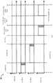
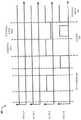
图1根据本公开的实施方式示意性示出了示例的保形膜沉积 (CFD)工艺的时序图。1 schematically illustrates a timing diagram of an example conformal film deposition (CFD) process in accordance with embodiments of the present disclosure.
图2根据本公开的实施方式示意性示出了另一示例的CFD工艺的时序图。FIG. 2 schematically illustrates a timing diagram of another example CFD process according to an embodiment of the present disclosure.
图3根据本公开的实施方式示意性示出了另一示例的CFD工艺的时序图。FIG. 3 schematically illustrates a timing diagram of another example CFD process according to an embodiment of the present disclosure.
图4根据本公开的实施方式示意性示出了一示例的包括等离子体处理循环的CFD工艺的时序图。4 schematically illustrates a timing diagram of an example CFD process including a plasma processing cycle, in accordance with embodiments of the present disclosure.
图5根据本公开的实施方式示出了所沉积的膜的湿法蚀刻速率比和沉积温度之间的示例的相关性。5 illustrates an example correlation between wet etch rate ratio and deposition temperature for a deposited film, according to an embodiment of the present disclosure.
图6根据本公开的实施方式示出了所沉积的膜的湿法蚀刻速率比和应力之间的示例的相关性。6 illustrates an example correlation between wet etch rate ratio and stress for a deposited film, according to an embodiment of the present disclosure.
图7根据本公开的实施方式示出了所沉积的膜的膜污染物浓度和沉积温度之间的示例的相关性。7 illustrates an example correlation between film contaminant concentration and deposition temperature of a deposited film, according to an embodiment of the present disclosure.
图8示意性地示出了包含多个空隙的非平坦的衬底的示例的横截面。FIG. 8 schematically illustrates a cross-section of an example of a non-planar substrate containing a plurality of voids.
图9根据本公开的实施方式示意性地示出了包括到PECVD工艺的过渡的示例的CFD工艺的时序图。9 schematically illustrates a timing diagram of an example CFD process including a transition to a PECVD process in accordance with an embodiment of the present disclosure.
图10示意性地示出了包含锁孔空穴的间隙填充的示例的横截面。Figure 10 schematically shows a cross-section of an example of a gap fill including a keyhole cavity.
图11根据本公开的实施方式示意性地示出了包括原位蚀刻的示例的 CFD工艺的时序图。11 schematically illustrates a timing diagram of an example CFD process including in-situ etching in accordance with an embodiment of the present disclosure.
图12A示意性地示出了重入(re-entrant)的间隙填充轮廓的示例的横截面。Figure 12A schematically shows a cross-section of an example of a re-entrant gap filling profile.
图12B根据本公开的实施方式示意性地示出了在原位蚀刻过程中图 12A的重入的间隙填充轮廓的示例的横截面。12B schematically illustrates a cross-section of an example of the reentrant gap-fill profile of FIG. 12A during an in-situ etch process, in accordance with an embodiment of the present disclosure.
图12C根据本公开的实施方式示意性地示出了在原位蚀刻过程中图 12B的间隙填充轮廓的示例的横截面。12C schematically illustrates a cross-section of an example of the gap-fill profile of FIG. 12B during an in-situ etch process, in accordance with an embodiment of the present disclosure.
图13根据本公开的实施方式示意性地示出了示例的处理站。Figure 13 schematically illustrates an example processing station in accordance with an embodiment of the present disclosure.
图14根据本公开的实施方式示意性地示出了包括多个处理站和控制器的示例性处理工具。14 schematically illustrates an exemplary processing tool including a plurality of processing stations and a controller in accordance with an embodiment of the present disclosure.
图15根据本公开的实施方式示意性地示出了在包括原位蚀刻的 CFD工艺过程中的硅通孔的示例的横截面图。15 schematically illustrates a cross-sectional view of an example of a TSV during a CFD process including in-situ etching, in accordance with an embodiment of the present disclosure.
图16示出了具有三维栅结构的晶体管,其中,源极和漏极形成在难以通过传统的离子注入技术掺杂的薄垂直结构中。Figure 16 shows a transistor with a three-dimensional gate structure in which the source and drain are formed in thin vertical structures that are difficult to dope by conventional ion implantation techniques.
图17呈现了随着时间沿x轴推进从左到右的基准CFD操作顺序。Figure 17 presents the baseline CFD sequence of operations advancing from left to right along the x-axis over time.
图18和19描绘了其中掺杂剂沉积在下伏衬底的界面处,随后CFD 循环与掺杂剂输送穿插,且任选地用未掺杂的保护性“加盖(capping)”层可以是CFD氧化膜结束的实施方式。Figures 18 and 19 depict where dopants are deposited at the interface of the underlying substrate, followed by CFD cycles interspersed with dopant delivery, and optionally with an undoped protective "capping" layer which can be Embodiment of CFD oxide film finish.
图20显示了用于合成CFD BSG/PSG膜的典型沉积框图。Figure 20 shows a typical deposition block diagram for synthesizing CFD BSG/PSG films.
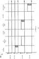
图21显示了在致密和隔离的结构上CFD膜的阶梯覆盖性计算为

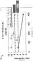
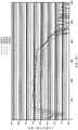
图22呈现了SIMS数据,其示出了在CFD膜中平均硼浓度可在约 0.5-3.5重量%硼的范围中调节。Figure 22 presents SIMS data showing that the average boron concentration in the CFD films can be adjusted in the range of about 0.5-3.5 wt% boron.
具体实施方式Detailed ways
半导体器件的制造通常涉及在集成制造工艺中在非平坦的衬底上沉积一个或多个薄膜。在集成工艺的一些方面,沉积与衬底形貌共形的薄膜可能是有用的。例如,氮化硅膜可以沉积在增高的栅极堆叠(elevated gate stack)的顶部作为间隔层以保护轻掺杂的源极和漏极区域免受随后的离子注入工艺的损坏。The fabrication of semiconductor devices typically involves depositing one or more thin films on a non-planar substrate in an integrated fabrication process. In some aspects of the integration process, it may be useful to deposit thin films that are conformal to the substrate topography. For example, a silicon nitride film can be deposited on top of an elevated gate stack as a spacer layer to protect the lightly doped source and drain regions from damage by subsequent ion implantation processes.
在间隔层沉积工艺中,化学气相沉积(CVD)工艺可用于在非平坦的衬底上形成氮化硅膜,然后对其各向异性蚀刻以形成间隔结构。然而,随着栅堆叠之间的距离减小,CVD气相反应的物质运输限制可能会导致“面包块”(“bread-loafing”)沉积效应。这些效应通常导致在栅堆叠的顶面出现较厚的沉积物并且在栅堆叠的底部角落出现较薄的沉积物。此外,由于一些管芯(die)可以有不同器件密度的区域,因此在整个晶片表面的物质运输效应可能会导致在管芯内和晶片内的膜厚度的变化。这些厚度的变化可能导致在一些区域的过蚀刻和在其他区域的蚀刻不足。这会降低器件的性能和/或管芯产量。Among the spacer layer deposition processes, a chemical vapor deposition (CVD) process can be used to form a silicon nitride film on a non-planar substrate, which is then anisotropically etched to form a spacer structure. However, as the distance between the gate stacks decreases, the species transport limitations of the CVD gas phase reaction may lead to a "bread-loafing" deposition effect. These effects typically result in thicker deposits at the top surface of the gate stack and thinner deposits at the bottom corners of the gate stack. Furthermore, since some dies may have regions of different device densities, species transport effects across the wafer surface may cause variations in film thickness within the die and within the wafer. These thickness variations can result in overetching in some areas and underetching in others. This can reduce device performance and/or die yield.
解决这些问题的一些方法包括原子层沉积(ALD)。相比于使用热激活气相反应以沉积膜的CVD工艺,ALD工艺使用表面介导沉积反应以逐层沉积薄膜。在一个示例的ALD工艺中,包括多个表面活性位点的衬底表面被暴露于气相分布的第一膜前体(P1)。P1的一些分子可以在衬底表面顶部形成凝聚相,其包括P1的化学吸附类物和物理吸附分子。然后将反应器抽空,以除去气相和物理吸附的P1,以便只有化学吸附类物留下。然后引入第二膜前体(P2)到反应器中,使得一些P2的分子吸附到衬底表面。可以再次抽空该反应器,这时去除未被约束的P2。接着,提供于衬底的热能激活P1 和P2的吸附分子之间的表面反应,形成膜层。最后,将该反应器抽空,以去除反应副产物和可能未反应的P1和P2,结束ALD循环。可以包括其他 ALD循环以增加膜的厚度。Some approaches to address these issues include atomic layer deposition (ALD). In contrast to CVD processes that use thermally activated gas phase reactions to deposit films, ALD processes use surface-mediated deposition reactions to deposit thin films layer by layer. In one example ALD process, a substrate surface including a plurality of surface active sites is exposed to a gas phase distributed first film precursor (P1). Some molecules of P1 can form a condensed phase on top of the substrate surface, which includes chemisorbed species and physisorbed molecules of P1. The reactor was then evacuated to remove gas phase and physisorbed P1 so that only chemisorbed species remained. The second membrane precursor (P2) is then introduced into the reactor, so that some of the molecules of P2 are adsorbed to the substrate surface. The reactor can be evacuated again, at which point unconstrained P2 is removed. Next, the thermal energy supplied to the substrate activates the surface reaction between the adsorbed molecules of P1 and P2 to form a film layer. Finally, the reactor is evacuated to remove reaction by-products and possibly unreacted P1 and P2, ending the ALD cycle. Additional ALD cycles can be included to increase the thickness of the film.
在一个示例中,根据投配步骤前体的暴露时间和前体的粘着系数,每个ALD循环可以沉积厚度在0.5和3埃之间的膜层。因此,当沉积超过几纳米厚的膜时,ALD工艺可能是耗时的。此外,一些前体可以具有长的暴露时间,以沉积保形膜,从而也可以降低晶片吞吐的时间。In one example, depending on the exposure time of the precursor in the dosing step and the adhesion coefficient of the precursor, each ALD cycle can deposit a film with a thickness between 0.5 and 3 Angstroms. Therefore, the ALD process can be time consuming when depositing films that are more than a few nanometers thick. Additionally, some precursors can have long exposure times to deposit conformal films, which can also reduce wafer throughput times.
保形膜也可以沉积在平坦的衬底上。例如,由包含不同类型膜的平坦堆叠层可以形成光刻图案化应用中的抗反射层。这样的抗反射层厚度可介于约100至1000埃之间,使得ALD工艺的吸引力不及CVD工艺。然而,相比于许多CVD工艺可能提供的晶片内厚度变化的容差,这样的抗反射层还可以具有晶片内厚度变化的较低的容差。例如,600埃厚的抗反射层可以有小于3埃的厚度范围的容差。Conformal films can also be deposited on flat substrates. For example, antireflection layers in lithographic patterning applications can be formed from flat stacks comprising different types of films. Such antireflection layer thicknesses may be between about 100 to 1000 angstroms, making ALD processes less attractive than CVD processes. However, such an antireflection layer may also have a lower tolerance for intra-wafer thickness variation than many CVD processes may provide. For example, a 600 angstrom thick antireflection layer may have a tolerance in the thickness range of less than 3 angstroms.
相应地,本发明提供了用于在非平坦的和平坦的衬底上提供等离子体激活的保形膜沉积(CFD)的工艺和设备的多个示例。这些示例包括在一些但不是在所有的CFD工艺中采用的多种特征。在这些特征中有:(1)消除或减少从反应室中“清扫”一种或两种反应物所需的时间,(2)提供至少一种反应物的连续流,同时让不同的反应物断续地流入到反应室中,(3)当反应物中的一种以气相存在时,而不是当所有的反应物被清除出反应室时,点燃等离子体,(4)用等离子体处理沉积的CFD膜以修改膜的性能,(5)通过 CFD沉积膜的第一部分后,通常在相同的反应室中,通过PECVD沉积膜的一部分,(6)在CFD的阶段之间蚀刻部分地沉积的膜,以及(7)通过仅对膜的沉积的循环插入杂质输送循环,对CFD膜掺杂。当然,上面所罗列的并不详尽。研究本说明书的其余部分,各种其它CFD特征将是显而易见的。Accordingly, the present invention provides various examples of processes and apparatus for providing plasma-activated conformal film deposition (CFD) on non-planar and planar substrates. These examples include various features employed in some but not all CFD processes. Among these features are: (1) eliminating or reducing the time required to "sweep" one or both reactants from the reaction chamber, (2) providing a continuous flow of at least one reactant while allowing different reactants Intermittent flow into the reaction chamber, (3) ignition of the plasma when one of the reactants is present in the gas phase rather than when all of the reactants have been purged out of the chamber, (4) treatment of the deposition with the plasma The CFD film to modify the properties of the film, (5) after depositing the first part of the film by CFD, usually in the same reaction chamber, depositing part of the film by PECVD, (6) etching the partially deposited film between stages of CFD film, and (7) doping the CFD film by inserting an impurity delivery cycle only for the deposition cycle of the film. Of course, the above list is not exhaustive. Various other CFD features will become apparent upon studying the remainder of this specification.
CFD“循环”的构思与这里所讨论的各种示例有关。一般来说,循环是执行一次表面沉积反应所需的最小组的操作。一个循环的结果是在衬底表面上产生至少部分膜层。通常情况下,CFD循环将只包括那些将每种反应物输送并吸附到衬底表面,且接着使这些吸附的反应物形成部分膜层所必需的步骤。当然,循环可包括若干辅助步骤,如清扫反应物或副产物中的一种,和/或处理所沉积的部分膜。一般情况下,循环包含仅仅一种情形的独特操作序列。作为示例,一个循环可以包括以下操作:(i)输送/吸附反应物A, (ii)输送/吸附反应物B,(ⅲ)将B清扫出反应腔室,以及(iv)施加等离子体以驱动A和B的表面反应,从而在表面上形成部分膜层。The idea of a CFD "cycle" is relevant to the various examples discussed here. In general, a cycle is the smallest set of operations required to perform a surface deposition reaction. The result of one cycle is the creation of at least a partial film on the surface of the substrate. Typically, a CFD cycle will include only those steps necessary to transport and adsorb each reactant to the substrate surface, and then allow these adsorbed reactants to form a partial film. Of course, the cycle may include several auxiliary steps, such as scavenging one of the reactants or by-products, and/or treating a portion of the film deposited. Typically, a loop contains a unique sequence of operations for only one case. As an example, one cycle may include the following operations: (i) deliver/adsorb reactant A, (ii) deliver/adsorb reactant B, (iii) sweep B out of the reaction chamber, and (iv) apply plasma to drive The surfaces of A and B react to form a partial film on the surface.
上述7种特征现在将作进一步讨论。在下面的描述中,考虑CFD反应,在该CFD反应中,一种或多种反应物吸附到衬底表面,然后通过与等离子体的相互作用,发生反应,从而在该表面上形成膜。The above seven characteristics will now be discussed further. In the following description, a CFD reaction is considered in which one or more reactants are adsorbed to a substrate surface and then, through interaction with a plasma, react to form a film on the surface.
特征1(反应物的连续流)-当反应物A在传统的ALD中正常不会流动时,让反应物A在CFD循环的一个或多个部分的过程中连续流到反应室。在传统的ALD中,反应物A流动只为了让该反应物吸附在衬底表面。在ALD循环的其他阶段,反应物A不流动。然而,根据本发明所描述的某些CFD示例,反应物A不仅在与其吸附有关的阶段期间流动,而且在执行吸附A的操作之外的CFD循环的阶段流动。例如,在许多示例中,在反应物A 流动到反应器中的同时,装置正投配第二反应物(本文称作反应物B)。因此,在CFD循环的至少一部分的期间,反应物A和B以气相共存。另外,反应物A可以流动,同时施加等离子体以驱动在衬底表面的反应。注意,可结合载气-如氩气将连续流动的反应物输送到反应室。Feature 1 (Continuous Flow of Reactants) - Let Reactant A flow continuously to the reaction chamber during one or more parts of the CFD cycle when it would not normally flow in conventional ALD. In conventional ALD, reactant A flows only to allow the reactant to be adsorbed on the substrate surface. During other stages of the ALD cycle, reactant A does not flow. However, according to certain CFD examples described herein, reactant A flows not only during the phases associated with its adsorption, but also during phases of the CFD cycle outside of the operation of performing adsorption of A. For example, in many instances, while reactant A is flowing into the reactor, the apparatus is dosing a second reactant (referred to herein as reactant B). Thus, during at least a portion of the CFD cycle, reactants A and B coexist in the gas phase. Alternatively, reactant A can flow while applying plasma to drive the reaction at the substrate surface. Note that a continuous flow of reactants can be delivered to the reaction chamber in combination with a carrier gas such as argon.
连续流的示例的一个优点是,所形成的流避免了由与开启流与关闭流相关的使流瞬态启动并稳定而导致的延迟以及流的变化。One advantage of the continuous flow example is that the resulting flow avoids the delays and changes in flow caused by transiently starting and stabilizing the flow associated with opening and closing the flow.
作为具体的示例,可通过保形膜沉积工艺,使用主要反应物(有时也被称为“固体组分”前体,或在本示例中,简单称作“反应物B”)沉积氧化膜。双(叔-丁基氨基)硅烷(BTBAS)是一种这样的主要反应物。在此示例中,氧化物沉积工艺涉及氧化剂的输送,如氧或一氧化二氮,其在不同的暴露阶段,在主要反应物的输送过程中,初始地并且连续地流动。在不同的等离子体暴露阶段,氧化剂也连续流动。参见例如图1中所示的序列。相比而言,在传统的ALD工艺中,当固体组分前体输送到反应器中时,氧化剂的流将停止。例如,当输送反应物B时,反应物A的流将停止。As a specific example, an oxide film may be deposited by a conformal film deposition process using a primary reactant (also sometimes referred to as a "solid component" precursor, or in this example, simply "reactant B"). Bis(tert-butylamino)silane (BTBAS) is one such primary reactant. In this example, the oxide deposition process involves the delivery of an oxidant, such as oxygen or nitrous oxide, which flows initially and continuously during the delivery of the primary reactants at various exposure stages. The oxidant also flows continuously during different plasma exposure stages. See, for example, the sequence shown in Figure 1 . In contrast, in conventional ALD processes, the flow of oxidant is stopped when the solid component precursor is delivered to the reactor. For example, when reactant B is being delivered, the flow of reactant A will stop.
在一些具体的示例中,连续流动的反应物是“辅助”的反应物。如本文所用,“辅助”的反应物是任何并非主要反应物的反应物。正如上文所述,主要反应物包含在室温下是固体的元素,该元素用于由CFD形成的膜。这样的元素的示例是金属(例如,铝和钛)、半导体(例如,硅和锗)、和非金属或类金属(例如,硼)。辅助的反应物的示例包括氧气、臭氧、氢、一氧化碳、一氧化二氮、氨、烷基胺、和其他类似物。In some specific examples, the continuously flowing reactants are "auxiliary" reactants. As used herein, an "auxiliary" reactant is any reactant that is not a primary reactant. As mentioned above, the primary reactants contain elements that are solid at room temperature, which are used in films formed by CFD. Examples of such elements are metals (eg, aluminum and titanium), semiconductors (eg, silicon and germanium), and non-metals or metalloids (eg, boron). Examples of auxiliary reactants include oxygen, ozone, hydrogen, carbon monoxide, nitrous oxide, ammonia, alkylamines, and the like.
连续流动的反应物可以以恒定的流率或以变动但可控的流率提供。在后者的情况下,作为示例,在输送主要反应物的暴露阶段期间,辅助反应物的流率可能下降。例如,在氧化物沉积过程中,氧化剂(例如,氧或一氧化二氮)在整个沉积序列可以连续流动,但是在输送主要反应物(例如, BTBAS)时,其流率可能下降。这在BTBAS的投配期间,会增加其局部压强,从而减少布满衬底表面所需要的暴露时间。点燃等离子体之前不久,氧化剂的流量可以增加,以减少等离子体暴露阶段期间BTBAS存在的可能性。在一些实施方式中,连续流动的反应物在两个或两个以上的沉积循环的过程中以变动的流率流动。例如,反应物可以在第一CFD循环以第一流率流动,而在第二CFD循环以第二流率流动。The continuously flowing reactants can be provided at a constant flow rate or at a variable but controllable flow rate. In the latter case, as an example, the flow rate of the secondary reactant may drop during the exposure phase in which the primary reactant is delivered. For example, during oxide deposition, the oxidant (eg, oxygen or nitrous oxide) may flow continuously throughout the deposition sequence, but its flow rate may decrease when delivering the primary reactant (eg, BTBAS). This increases the local pressure of the BTBAS during dosing, thereby reducing the exposure time required to fill the substrate surface. Shortly before igniting the plasma, the flow of oxidant can be increased to reduce the likelihood of the presence of BTBAS during the plasma exposure phase. In some embodiments, the continuously flowing reactants flow at varying flow rates during two or more deposition cycles. For example, the reactants may flow at a first flow rate in the first CFD cycle and flow at a second flow rate in the second CFD cycle.
当采用多个反应物且其中之一的流动是连续的时,在CFD循环的一部分的过程中,其中的至少两者将以气相共存。同样,在输送第一反应物后没有执行清除步骤时,两种反应物将共同存在。因此,使用在没有施加激活能量的气相中不会彼此明显发生反应的反应物可能是重要的。通常情况下,反应物应当直到其出现在衬底表面上并暴露于等离子体或另一合适的非热激活条件时才反应。选择这样的反应物涉及考虑至少(1)所希望的反应的热力学适宜度(吉布斯自由能<0),和(2)反应的激活能量,其应该是足够大,以便在所需的沉积温度的反应可以忽略不计。When multiple reactants are employed and the flow of one of them is continuous, at least two of them will coexist in the gas phase during part of the CFD cycle. Likewise, when no clean-up step is performed after delivery of the first reactant, the two reactants will co-exist. Therefore, it may be important to use reactants that do not appreciably react with each other in the gas phase where no activation energy is applied. Typically, the reactant should not react until it is present on the substrate surface and exposed to plasma or another suitable non-thermal activation condition. Selection of such reactants involves consideration of at least (1) the desired thermodynamic fitness of the reaction (Gibbs free energy < 0), and (2) the activation energy of the reaction, which should be large enough to allow deposition at the desired The temperature response is negligible.
特征2(减少或消除清扫步骤)-在某些实施方式中,该工艺省去或减少与清扫步骤相关联的时间,清扫步骤在传统的ALD中通常会执行。在传统的ALD中,在每种反应物输送并吸附到衬底表面后,进行单独的清扫步骤。在传统的ALD清扫步骤中,很少或没有吸附或反应发生。在CFD循环中,在输送至少一种反应物后,减少或消除该清扫步骤。图1示出了去除了清扫步骤的处理序列的示例。没有执行从反应室清扫反应物A的清扫步骤。在某些情况下,在CFD循环输送第一反应物后,没有进行清扫步骤,但是在输送第二反应物或者最后输送的反应物输送后,可以选择地进行清扫步骤。Feature 2 (Reduce or Eliminate Sweeping Steps) - In certain embodiments, the process eliminates or reduces the time associated with sweeping steps that are typically performed in conventional ALD. In conventional ALD, after each reactant is transported and adsorbed to the substrate surface, a separate sweeping step is performed. In traditional ALD sweep steps, little or no adsorption or reaction occurs. In a CFD cycle, this sweep step is reduced or eliminated after the delivery of at least one reactant. Figure 1 shows an example of a processing sequence with the cleaning step removed. The purge step to purge reactant A from the reaction chamber was not performed. In some cases, the cleaning step is not performed after the CFD cycle delivers the first reactant, but may optionally be performed after delivering the second reactant or the last reactant delivered.
CFD的“清扫”步骤或阶段的构思出现在本发明的各种实施方式的讨论中。一般来说,清扫阶段从反应室去除或清除气相反应物中的一种,并且通常仅在该反应物的输送完成后进行。换言之,该反应物在清扫阶段不再输送到反应室。然而,在清扫阶段期间,该反应物保持吸附在衬底表面上。通常情况下,清扫用于在衬底表面吸附该反应物至所需的水平后去除室中的任何残留的气相反应物。清扫阶段也可以从所述衬底表面去除弱吸附的物质(例如,某些前体配位体或反应副产物)。在ALD中,清扫阶段对于防止两种反应物的气相反应或者防止一种反应物与热的、等离子体的相互作用或者用于表面反应的其他的驱动力的相互作用而言,被视为是必要的。在一般情况下,并且除非另有规定,否则,清扫阶段可通过以下步骤完成:(ⅰ)将反应室抽空,和/或(ii)使不包含将被清扫出的物质的气体流动通过该反应室。在情形(ii)中,这样的气体可以是,例如,惰性气体或辅助反应物,如连续流动的辅助反应物。The concept of a "sweep" step or stage of CFD appears in the discussion of various embodiments of the present invention. In general, the purge stage removes or purges one of the gas-phase reactants from the reaction chamber, and usually occurs only after delivery of that reactant is complete. In other words, the reactant is no longer delivered to the reaction chamber during the purge phase. However, during the sweep phase, the reactants remain adsorbed on the substrate surface. Typically, sweeping is used to remove any residual gas-phase reactants in the chamber after the substrate surface has adsorbed the reactants to the desired level. The sweeping stage can also remove weakly adsorbed species (eg, certain precursor ligands or reaction by-products) from the substrate surface. In ALD, the sweeping stage is considered to prevent the gas phase reaction of the two reactants or the interaction of one reactant with heat, plasma, or other driving forces for surface reactions. necessary. In general, and unless otherwise specified, the purge phase may be accomplished by (i) evacuating the reaction chamber, and/or (ii) flowing a gas that does not contain the species to be purged through the reaction room. In case (ii), such gas may be, for example, an inert gas or an auxiliary reactant, such as a continuous flow auxiliary reactant.
消除清扫阶段可以在有或无其它反应物的连续流的情况下完成。在图1中所示的实施方式中,反应物A在其到衬底表面上的吸附完成后,没有被清扫掉,而是继续流入(图中由标号130示出)。The elimination sweep stage can be accomplished with or without continuous flow of other reactants. In the embodiment shown in FIG. 1, the reactant A is not swept away after its adsorption to the substrate surface is complete, but continues to flow in (indicated by the
在使用两个或两个以上的反应物的各种实施方式中,其清扫步骤被消除或减少的反应物是辅助反应物。作为示例,辅助反应物是氧化剂或氮源,而主要反应物是含硅、硼、或锗的前体。当然,主要反应物的清扫也可以被减少或消除。在一些实施方式中,在辅助反应物输送之后,不执行清扫步骤,但在主要反应物输送之后,可选地执行清扫步骤。In various embodiments using two or more reactants, the reactant whose sweep step is eliminated or reduced is a secondary reactant. As an example, the secondary reactant is an oxidant or nitrogen source, and the primary reactant is a silicon, boron, or germanium containing precursor. Of course, sweeping of the primary reactants can also be reduced or eliminated. In some embodiments, a purge step is not performed after the secondary reactant delivery, but optionally a purge step is performed after the primary reactant delivery.
如所提及的,清扫阶段不必完全消除,而只是相比于传统的ALD工艺清扫阶段减少持续时间。例如,在CFD循环过程中,诸如辅助反应物之类的反应物的清扫阶段可进行约0.2秒或更短,例如,介于约0.001至0.1秒之间。As mentioned, the sweep phase does not have to be eliminated completely, but only of reduced duration compared to conventional ALD processes. For example, during a CFD cycle, the purge phase of reactants such as auxiliary reactants may be performed for about 0.2 seconds or less, eg, between about 0.001 to 0.1 seconds.
特征3(当反应物中的一种以气相存在时点燃等离子体)-对于该特征,点燃等离子体,然后将所有的反应物从反应室中清除。这与传统的 ALD工艺相反,在传统的ALD工艺中,只有气相反应物不再存在于反应室中后,才激活等离子体或进行其他反应驱动操作。注意,在如图1所描绘的 CFD循环的等离子体部分的期间反应物A连续流动时,这样的特征必然会发生。然而,本公开的实施方式并不限于这种方式。一种或多种反应物可以在 CFD循环的等离子体阶段流动,但不必在CFD循环过程中连续流动。此外,在等离子体激活过程中处于气相的反应物可以是主要反应物或辅助反应物 (当在CFD循环中采用两种反应物时)。Feature 3 (Ignition of the plasma when one of the reactants is present in the gas phase) - For this feature, the plasma is ignited and then all reactants are purged from the reaction chamber. This is in contrast to conventional ALD processes, where plasma activation or other reaction-driven operations are performed only after gas-phase reactants are no longer present in the reaction chamber. Note that such a feature necessarily occurs when reactant A flows continuously during the plasma portion of the CFD cycle as depicted in Figure 1 . However, embodiments of the present disclosure are not limited in this manner. One or more reactants may flow during the plasma phase of the CFD cycle, but need not flow continuously during the CFD cycle. In addition, the reactants in the gas phase during plasma activation can be the primary reactant or the secondary reactant (when both reactants are employed in the CFD cycle).
例如,序列可以是:(i)引入反应物A,(ii)清除A,(iii)引入反应物B并且当B正在流动时激励等离子体,及(iv)清除。在这样的实施方式中,该工艺采用来源于气相的等离子体激活反应物。这是一个一般的示例,其中CFD不限于序列步骤的序列。For example, the sequence can be: (i) introduce reactant A, (ii) purge A, (iii) introduce reactant B and energize the plasma while B is flowing, and (iv) purge. In such embodiments, the process employs plasma-activated reactants originating from the gas phase. This is a general example where CFD is not limited to a sequence of sequential steps.
如果在向反应器供应固体组分前体(主要反应物)的时间阶段提供激活等离子体,则阶梯覆盖性(step coverage)可能变得不那么保形,但沉积速率通常会增大。但是,如果只有在输送一种辅助反应物的过程中进行等离子体激活,情况并不一定是如此。等离子体可以激活气相辅助成分以使其更易反应,从而增加其在保形膜沉积反应中的反应性。在某些实施方式中,该特征在沉积含硅膜(例如氧化物、氮化物或碳化物)时采用。Step coverage may become less conformal if the activation plasma is provided during the time period during which the solid component precursors (primary reactants) are supplied to the reactor, but deposition rates generally increase. However, this is not necessarily the case if plasma activation occurs only during the delivery of an auxiliary reactant. The plasma can activate gas-phase auxiliary components to make them more reactive, thereby increasing their reactivity in conformal film deposition reactions. In certain embodiments, this feature is employed when depositing silicon-containing films such as oxides, nitrides, or carbides.
特征4(沉积CFD膜的等离子体处理)-在这些实施方式中,等离子体在保形膜沉积过程中可起到两种或两种以上的作用。其作用之一是,在每个CFD循环中激活或驱动膜形成反应。其另一个作用是,在经过一个或多个CFD循环的CFD膜部分或完全沉积之后,处理膜。等离子体处理的目的是改变膜的一种或多种属性。通常情况下,但并不一定,进行等离子体处理阶段的条件与那些用于激活膜形成反应(即,驱动膜形成反应)而采用的条件是不同的。作为一个例子,等离子体处理也可以在还原或氧化环境存在时进行(例如,在氢或氧存在时),而这在CFD循环的激活期间是不必要的。Feature 4 (Plasma Treatment for Deposition of CFD Films) - In these embodiments, the plasma can perform two or more roles in the conformal film deposition process. One of its roles is to activate or drive the membrane formation reaction in each CFD cycle. Another function of this is to process the film after partial or complete deposition of the CFD film over one or more CFD cycles. The purpose of plasma treatment is to alter one or more properties of the film. Typically, but not necessarily, the conditions under which the plasma treatment stage is carried out are different from those employed to activate the film-forming reaction (ie, drive the film-forming reaction). As an example, plasma treatment can also be performed in the presence of a reducing or oxidizing environment (eg, in the presence of hydrogen or oxygen), which is not necessary during activation of a CFD cycle.
可以在CFD工艺的每个循环期间、每隔一个循环期间、或在更少频率的基础上,执行等离子体处理操作。该处理可以是定期进行的、与固定的 CFD循环数相结合的,或者其可以可变地(例如,在CFD循环的不同的间隔)或者甚至是随机地执行。在一个典型的例子中,进行几个CFD循环的膜沉积,以达到适当的膜厚度,然后采用等离子体处理。此后,再次进行没有等离子体处理的几个CFD循环的膜沉积,然后再次进行等离子体处理。这种 x次CFD循环的超序列及紧接着的等离子体处理(膜改性),可以重复进行,直到膜通过CFD完全形成。Plasma processing operations may be performed during every cycle of the CFD process, during every other cycle, or on a less frequent basis. The processing may be performed periodically, in conjunction with a fixed number of CFD cycles, or it may be performed variably (eg, at different intervals of a CFD cycle) or even randomly. In a typical example, several CFD cycles of film deposition are performed to achieve the appropriate film thickness, followed by plasma treatment. Thereafter, film deposition was performed again for several CFD cycles without plasma treatment, followed by plasma treatment again. This supersequence of x CFD cycles followed by plasma treatment (film modification) can be repeated until the film is fully formed by CFD.
在某些实施方式中,所述等离子体处理可在CFD循环开始之前进行,以改变沉积CFD膜的表面的一种或多种属性。在各种实施方式中,表面是由硅(掺杂的或不掺杂的)或含硅物质形成的。改变后的表面能够更好地产生与随后沉积的CFD膜之间的高品质界面。该界面可通过诸如减少故障而提供例如良好的附着力、可靠的电气性能等。In certain embodiments, the plasma treatment may be performed prior to the initiation of a CFD cycle to alter one or more properties of the surface on which the CFD film is deposited. In various embodiments, the surface is formed of silicon (doped or undoped) or a silicon-containing species. The altered surface is better able to produce high-quality interfaces with subsequently deposited CFD films. The interface may provide eg good adhesion, reliable electrical performance, etc. by, for example, reducing failures.
衬底在CFD之前的预处理,并不限于任何特定的等离子体处理。在某些实施方式中,预处理涉及,在氦、氢、氩、氮、氢/氮形成气体、和/或氨的存在下,暴露于氢等离子体、氮等离子体、氮/氢等离子体、氨等离子体、氩等离子体、氦等离子体、氦退火、氢退火、氨退火、和UV-固化。等离子体处理可以用各种等离子体发生器实现,包括但不限于,用微波、ICP-远程、ICP-直接(direct)和本领域技术人员公知的其他手段来实现。The pretreatment of the substrate prior to CFD is not limited to any particular plasma treatment. In certain embodiments, the pretreatment involves exposure to hydrogen plasma, nitrogen plasma, nitrogen/hydrogen plasma, Ammonia plasma, argon plasma, helium plasma, helium anneal, hydrogen anneal, ammonia anneal, and UV-curing. Plasma treatment can be accomplished with a variety of plasma generators, including, but not limited to, microwave, ICP-remote, ICP-direct, and other means known to those skilled in the art.
总体而言,该处理可发生在CFD循环之前、期间和之后。当在 CFD循环期间发生时,可以根据适当的沉积条件选择处理频率。通常情况下,处理发生的频率每个循环不超过一次。In general, the processing can take place before, during and after the CFD cycle. As occurs during a CFD cycle, the treatment frequency can be selected according to appropriate deposition conditions. Typically, processing occurs no more than once per cycle.
作为一个例子,考虑从存在有一些碳的前体形成氮化硅的工艺。这类前体的示例包括BTBAS。作为前体中存在有碳的后果,所沉积的氮化物膜包括一些碳杂质,这可能会降低氮化物的电性能。为了克服这种问题,在使用含碳前体的几个CFD循环后,部分沉积的膜在等离子体的存在下暴露于氢,以减少并最终去除碳杂质。As an example, consider a process for forming silicon nitride from a precursor in which some carbon is present. Examples of such precursors include BTBAS. As a consequence of the presence of carbon in the precursor, the deposited nitride film includes some carbon impurities, which may degrade the electrical properties of the nitride. To overcome this problem, after several CFD cycles using carbon-containing precursors, partially deposited films are exposed to hydrogen in the presence of plasma to reduce and ultimately remove carbon impurities.
可以选择用于修改膜表面的等离子体条件,以实现膜性质和/或组成物的所希望的改变。在各个等离子体条件中,对于所需修改,可以选择和/或修整的是:氧化条件、还原条件、蚀刻条件、用于产生等离子体的功率、用于产生等离子体的频率、用于产生等离子体的两种或更多的频率的使用、等离子体密度、等离子体和衬底之间的距离,等等。CFD膜可以通过等离子体处理进行修改的性能的示例包括:内部膜应力、耐蚀刻性、密度、硬度、光学性质(折射率、反射率、光密度、等等)、介电常数、碳含量、电性能 (Vfb扩散等)、及类似物。The plasma conditions used to modify the film surface can be selected to achieve desired changes in film properties and/or composition. Among the various plasma conditions, what can be selected and/or tailored for the desired modification are: oxidizing conditions, reducing conditions, etching conditions, power used to generate plasma, frequency used to generate plasma, used to generate plasma The use of two or more frequencies of the volume, the plasma density, the distance between the plasma and the substrate, etc. Examples of properties of CFD films that can be modified by plasma treatment include: internal film stress, etch resistance, density, hardness, optical properties (refractive index, reflectivity, optical density, etc.), dielectric constant, carbon content, Electrical properties (Vfb diffusion, etc.), and the like.
在一些实施方式中,使用除等离子体处理以外的处理,以修改沉积膜的属性。这样的处理包括电磁辐射处理、热处理(例如,退火或高温脉冲)、及类似处理。任何这些处理可以单独进行,或者与包括等离子体处理的另一种处理组合进行。任何这样的处理可以用来替代任何上述等离子体处理。在一个特定的实施方式中,该处理涉及把该膜暴露于紫外线辐射。正如下面所描述的,在一个特定的实施方式中,该方法涉及对CFD膜氧化物在原位(即,在形成膜的过程中)应用UV-辐射或对沉积后的氧化物应用UV-辐射。这样的处理可以用来减少或消除结构缺陷,并提供改进的电性能。In some embodiments, treatments other than plasma treatments are used to modify the properties of the deposited films. Such treatments include electromagnetic radiation treatments, thermal treatments (eg, annealing or high temperature pulses), and the like. Any of these treatments can be performed alone or in combination with another treatment including plasma treatment. Any such treatment can be used in place of any of the plasma treatments described above. In a specific embodiment, the treatment involves exposing the film to ultraviolet radiation. As described below, in a specific embodiment, the method involves applying UV-radiation to the CFD film oxide in situ (ie, during film formation) or to the deposited oxide. . Such treatments can be used to reduce or eliminate structural defects and provide improved electrical properties.
在某些特定的实施方式中,UV处理可以和等离子体处理结合使用。这两种操作可以同时执行或顺序执行。在顺序执行选项中,可选地, UV操作首先发生。在同时执行的选项中,这两个处理可以配置不同的源 (例如,RF功率源用于等离子体,灯用于UV),或配置单一的源,例如氦等离子体,其产生紫外线辐射副产物。In certain specific embodiments, UV treatment can be used in conjunction with plasma treatment. Both operations can be performed simultaneously or sequentially. In the sequential execution option, optionally, the UV operation happens first. In a simultaneous option, the two processes can be configured with different sources (eg, RF power source for plasma, lamp for UV), or a single source, such as helium plasma, which produces UV radiation by-products .
特征5(通过CFD并且接着过渡到PECVD进行沉积)-在这样的实施方式中,已完成的膜中部分由CFD产生,且部分由诸如PECVD等CVD 工艺产生。通常情况下,沉积工艺的CFD部分首先进行,PECVD部分其次进行,但这并不是必然的。与仅用CVD相比,混合CFD/CVD工艺可以改善阶梯覆盖性(step coverage),与仅用CFD相比,混合CFD/CVD工艺还额外地提高了沉积速率。在某些情况下,当CFD反应物正在流动时,施用等离子体或其他激励,以产生寄生CVD操作,从而实现较高的沉积速率、不同级别的膜,等等。Feature 5 (Deposition by CFD and then transition to PECVD) - In such an embodiment, the finished film is produced partly by CFD and partly by a CVD process such as PECVD. Typically, the CFD portion of the deposition process is performed first, and the PECVD portion is performed second, but this is not necessarily the case. The hybrid CFD/CVD process can improve step coverage compared to CVD alone, and the hybrid CFD/CVD process additionally increases the deposition rate compared to CFD alone. In some cases, while the CFD reactants are flowing, a plasma or other excitation is applied to create parasitic CVD operations, enabling higher deposition rates, different grades of film, and the like.
在某些实施方式中,可以采用两个或更多的CFD阶段,和/或可以采用两个或更多的CVD阶段。例如,膜的初始部分可通过CFD沉积,随后膜的中间部分通过CVD沉积,且膜的最后部分通过CFD沉积。在这样的实施方式中,在通过CFD沉积膜的后面的部分之前,诸如通过等离子体处理或蚀刻修改膜的CVD部分,可能是需要的。In certain embodiments, two or more CFD stages may be employed, and/or two or more CVD stages may be employed. For example, an initial portion of the film may be deposited by CFD, followed by a middle portion of the film by CVD, and a final portion of the film by CFD. In such embodiments, it may be desirable to modify the CVD portion of the film, such as by plasma treatment or etching, before depositing the latter portion of the film by CFD.
在CFD阶段和CVD阶段之间可以采用过渡阶段。在这样的过渡阶段中采用的条件,与在CFD阶段或CVD阶段所采用的条件不同。通常情况下,虽然并不一定,该条件同时允许CFD表面反应和CVD类型气相反应。过渡阶段通常涉及暴露在等离子体中,其例如可以是脉冲的。另外,在过渡阶段,可以涉及以低流率(即,速率明显低于该工艺中相应的CFD阶段所采用的速率)输送一种或多种反应物。A transition phase may be employed between the CFD phase and the CVD phase. The conditions employed in such a transition stage are different from those employed in the CFD stage or the CVD stage. Typically, though not necessarily, this condition allows both CFD surface reactions and CVD-type gas-phase reactions. The transition phase typically involves exposure to plasma, which may be pulsed, for example. Additionally, during the transition stage, it may involve delivering one or more reactants at low flow rates (ie, at rates significantly lower than those employed in the corresponding CFD stage of the process).
特征6(通过CFD沉积,蚀刻,然后进一步通过CFD沉积)-在这样的实施方式中,进行一个或多个循环(通常是多个循环)的CFD沉积,然后将得到的膜进行蚀刻以去除,例如,在凹部入口(尖端)处或附近的一些多余的膜,然后进一步进行CFD的沉积循环。沉积膜中结构特征的其他实施例,可以以类似方式蚀刻。用于该工艺的蚀刻剂的选择将取决于被蚀刻材料。在某些情况下,可以用含氟蚀刻剂(例如,NF3)或氢进行蚀刻操作。Feature 6 (deposited by CFD, etched, then further deposited by CFD) - In such embodiments, one or more cycles (usually multiple cycles) of CFD deposition are performed, and the resulting film is then etched to remove, For example, some excess film at or near the entrance (tip) of the recess, and then a further CFD deposition cycle. Other embodiments of structural features in the deposited film can be etched in a similar manner. The choice of etchant for this process will depend on the material being etched. In some cases, the etching operation may be performed with a fluorine-containing etchant (eg, NF3) or hydrogen.
在某些实施方式中,用远程等离子体来产生蚀刻剂。一般来说,相较于直接等离子体,远程等离子体蚀刻具有更好的各向同性。远程等离子体通常对衬底提供相对较高比例的自由基。这些自由基的反应性可以随在凹部内的垂直位置的变化而变化。在特征的顶部,自由基较为集中,因而会以较高的速率蚀刻,而朝凹部进一步向下及在底部,部分自由基已丢失,因此,它们以较低的速率蚀刻。当然,这是一种理想的反应性分布,用于解决发生在凹部开口处太多沉积的问题。在蚀刻中使用远程等离子体的额外好处是等离子体相对和缓,因此不可能损坏衬底层。当下伏的衬底层对氧化或其他损坏敏感时,这是特别有益的。In certain embodiments, a remote plasma is used to generate the etchant. In general, remote plasma etching is more isotropic than direct plasma. Remote plasmas typically provide a relatively high proportion of free radicals to the substrate. The reactivity of these radicals can vary with the vertical position within the recess. At the top of the feature, the free radicals are more concentrated and etch at a higher rate, while further down the recess and at the bottom, some of the free radicals are lost, so they etch at a lower rate. Of course, this is an ideal reactivity profile to address the problem of too much deposition occurring at the recess openings. An additional benefit of using a remote plasma in etching is that the plasma is relatively gentle and therefore unlikely to damage the substrate layers. This is particularly beneficial when the underlying substrate layer is sensitive to oxidation or other damage.
特征7(用额外的反应物修整膜的成分)-本文提出的许多实施方式涉及采用一种或两种反应物的CFD工艺。另外,许多示例在每一个CFD循环中采用相同的反应物。然而,这并不是必然的。首先,许多CFD工艺可使用3种或更多的反应物。示例包括(i)使用乙硼烷、六氟化钨、和氢作为反应物的钨CFD;和(ii)使用乙硼烷、BTBAS、和氧作为反应物的硅氧化物CFD。乙硼烷可以从生长中的膜中除去,或,如果合适的话,它可以被并入膜中。Feature 7 (Trimming of Film Composition with Additional Reactants) - Many of the embodiments presented herein involve CFD processes employing one or two reactants. Additionally, many of the examples employed the same reactants in each CFD cycle. However, this is not inevitable. First, many CFD processes can use 3 or more reactants. Examples include (i) tungsten CFD using diborane, tungsten hexafluoride, and hydrogen as reactants; and (ii) silicon oxide CFD using diborane, BTBAS, and oxygen as reactants. Diborane can be removed from the growing film, or, if appropriate, it can be incorporated into the film.
此外,一些示例可以仅仅在某些CFD循环中采用额外的反应物。在这样的示例中,基本的CFD工艺循环仅仅采用创建基膜组合物的反应物(例如,氧化硅或碳化硅)。在所有或几乎所有的CFD循环中进行这个基本方法。然而,一些CFD循环作为不同的循环进行,且它们使用不同于正常沉积循环的条件。例如,它们可以采用一种或更多的额外反应物。这些不同的循环也可以采用与基本CFD工艺中所用的反应物相同的反应物,尽管这并不是必然的。Furthermore, some examples may employ additional reactants only in certain CFD cycles. In such an example, the basic CFD process cycle employs only the reactants (eg, silicon oxide or silicon carbide) that create the base film composition. Do this basic method in all or almost all CFD cycles. However, some CFD cycles are performed as different cycles, and they use different conditions than normal deposition cycles. For example, they may employ one or more additional reactants. These different cycles may also employ the same reactants as those used in the basic CFD process, although this is not required.
这样的CFD工艺对于制备掺杂的氧化物或其他掺杂的物质作为 CFD膜是特别有益的。在一些实施方式中,掺杂剂前体仅仅在一小部分CFD 循环中被包括作为“额外”的反应物。添加掺杂剂的频率取决于所期望的掺杂剂浓度。例如,在每10个基本物质沉积循环中可以有一个循环包含掺杂剂前体。Such CFD processes are particularly beneficial for preparing doped oxides or other doped species as CFD films. In some embodiments, dopant precursors are included as "additional" reactants in only a small fraction of the CFD cycles. The frequency of dopant addition depends on the desired dopant concentration. For example, dopant precursors may be included in one cycle out of every 10 base species deposition cycles.
不同于许多其他的沉积工艺,尤其是那些需要热激活的工艺,CFD 工艺可在相对较低的温度下进行。一般来说,CFD的温度在约20至400℃之间。可以选择这样的温度,以允许在温度敏感工艺的背景下沉积(例如在光致抗蚀剂的芯(core)的沉积)。在一个特定的实施方式中,约20至100℃之间的温度被用于双重图案化应用(使用,例如,光致抗蚀剂的芯)。在另一个实施方式中,约200至350℃之间的温度用于存储器制造处理(memoryfabrication processing)。Unlike many other deposition processes, especially those that require thermal activation, CFD processes can be performed at relatively low temperatures. Generally, the temperature of CFD is between about 20 and 400°C. Such temperatures may be chosen to allow deposition in the context of temperature sensitive processes (eg deposition in the core of a photoresist). In a specific embodiment, temperatures between about 20 and 100°C are used for double patterning applications (using, for example, photoresist cores). In another embodiment, temperatures between about 200 to 350° C. are used for memory fabrication processing.
如上文所述,CFD非常适合于在先进技术节点沉积膜。因此,例如,CFD工艺可以集成于在32纳米节点、22纳米节点、16纳米节点、11纳米节点、和超过这些的工艺中。这些节点描述在半导体国际技术路线图 (ITRS)中,业内人士多年来对微电子技术要求达成了共识。一般来说,它们引用存储单元的半节距。在一个特定的示例中,CFD工艺被应用到“2X”设备(具有在20-29nm范围内的特征的设备)和更精细的设备。As mentioned above, CFD is well suited for depositing films at advanced technology nodes. Thus, for example, CFD processes can be integrated in processes at the 32 nm node, 22 nm node, 16 nm node, 11 nm node, and beyond. These nodes are described in the International Technology Roadmap for Semiconductors (ITRS), the industry consensus on microelectronics technology requirements for many years. Generally, they refer to the half-pitch of the memory cells. In one specific example, the CFD process is applied to "2X" devices (devices with features in the 20-29 nm range) and finer devices.
虽然本文提供的CFD膜的例子大多数涉及硅基微电子器件,但该些膜也可以用于其他领域。使用非硅半导体(例如GaAs和其它III-V族半导体,以及II-VI族材料(例如HgCdTe))的微电子或光电子,可以得益于本文所公开的CFD工艺。保形介电膜在太阳能领域(例如光电器件)、电致变色领域、和其他领域的应用是可能的。While most of the examples of CFD films provided herein relate to silicon-based microelectronic devices, the films can be used in other fields as well. Microelectronics or optoelectronics using non-silicon semiconductors such as GaAs and other III-V semiconductors, as well as II-VI materials such as HgCdTe, can benefit from the CFD processes disclosed herein. Applications of conformal dielectric films in the solar field (eg optoelectronic devices), electrochromic field, and other fields are possible.
图1示意性地显示了等离子体激活CFD工艺的示例性实施方式的时序图100。描述了两个完整的CFD循环。如图所示,每一个都包括暴露于反应物A阶段120A或120B,紧接着暴露于反应物B阶段140A或140B,清扫反应物B阶段160A或160B,和最后等离子体激活阶段180A或180B。在等离子体激活阶段180A和180B期间提供的等离子体能量激活表面吸附的反应物A和B之间的反应。在所描述的实施方式中,一种反应物(反应物A)被传送之后不进行清扫阶段。事实上,这种反应物在膜沉积处理期间连续地流动。从而,当反应物A处于气相时,点燃等离子体。上述特征1-3体现在图 1的例子中。FIG. 1 schematically shows a timing diagram 100 of an exemplary embodiment of a plasma activated CFD process. Two complete CFD cycles are described. As shown, each includes exposure to reactant A
在所示实施方式中,反应物气体A和B可以在气相中共存而不相互反应。因此,在ALD工艺中描述的一个或多个处理步骤可以在这个示例的 CFD工艺中缩短或消除。例如,可以消除A暴露阶段120A和120B之后的清扫步骤。In the embodiment shown, the reactant gases A and B may coexist in the gas phase without reacting with each other. Accordingly, one or more of the processing steps described in the ALD process may be shortened or eliminated in the CFD process of this example. For example, cleaning steps after A exposure stages 120A and 120B can be eliminated.
CFD工艺可以用于沉积任何数量的不同类型的膜。虽然本文提出的大多数示例涉及介电材料,但所公开的CFD工艺也可用于形成导电性材料膜和半导体材料膜。氮化物和氧化物是特征性的介电材料,但也可以形成碳化物、氮氧化物、碳掺杂的氧化物、硼化物等等。氧化物包括的材料范围很广,包括未掺杂的硅酸盐玻璃(USG)、掺杂的硅酸盐玻璃。掺杂的玻璃的示例包括掺硼硅酸盐玻璃(BSG)、磷掺杂的硅酸盐玻璃(PSG)、硼磷掺杂的硅酸盐玻璃(BPSG)。CFD processes can be used to deposit any number of different types of films. While most of the examples presented herein involve dielectric materials, the disclosed CFD process can also be used to form films of conductive and semiconductive materials. Nitrides and oxides are characteristic dielectric materials, but carbides, oxynitrides, carbon-doped oxides, borides, and the like can also be formed. Oxides include a wide range of materials including undoped silicate glass (USG), doped silicate glass. Examples of doped glasses include borosilicate glass (BSG), phosphorus doped silicate glass (PSG), boron phosphorus doped silicate glass (BPSG).
在一些实施方式中,硅氮化物膜可以通过含硅反应物与一种或更多的含氮反应物和/或含氮反应物的混合物之间的反应形成。含硅反应物的实施例包括,但不限于,双(叔丁基氨基)硅烷(SiH2(NHC(CH3)3)2或BTBAS),二氯甲硅烷(SiH2Cl2),和氯硅烷(SiH3Cl)。含氮反应物的示例包括,但不限于,氨、氮、和叔丁基胺((CH3)3CNH2或叔丁基胺)。含氮反应物混合物的示例包括,但不限于,氮和氢的混合物。In some embodiments, the silicon nitride film may be formed by reaction between a silicon-containing reactant and one or more nitrogen-containing reactants and/or a mixture of nitrogen-containing reactants. Examples of silicon-containing reactants include, but are not limited to, bis(tert-butylamino)silane (SiH2(NHC(CH3 )3)2orBTBAS ), dichlorosilane (SiH2Cl2) , and chlorine Silane (SiH3Cl ). Examples of nitrogen-containing reactants include, but are not limited to, ammonia, nitrogen, and tert-butylamine ((CH3 )3CNH2 or tert- butylamine). Examples of nitrogen-containing reactant mixtures include, but are not limited to, mixtures of nitrogen and hydrogen.
可根据各种膜和/或硬件条件选择一种或多种反应物。例如,在一些实施方式中,硅氮化物膜可以由二氯硅烷和等离子体激活氮反应形成。把二氯硅烷化学吸附至硅氮化物表面可创设出硅-氢封端的表面,释放出氯化氢 (HCl)。该化学吸附反应的示例示意性地描述在反应1中。One or more reactants can be selected based on various membrane and/or hardware conditions. For example, in some embodiments, a silicon nitride film may be formed by reacting dichlorosilane and plasma-activated nitrogen. Chemisorption of dichlorosilane to silicon nitride surfaces creates a silicon-hydrogen terminated surface that releases hydrogen chloride (HCl). An example of this chemisorption reaction is schematically depicted in
反应1

反应1中所示的环状中间体可接着通过与等离子体激活氮的反应被转化成硅胺封端的表面。The cyclic intermediate shown in
然而,二氯硅烷的一些分子可通过其他的机制化学吸附。例如,表面形貌可阻碍反应1中描绘的环状中间体的形成。另一种化学吸附机制的示例示意性地显示于反应2中。However, some molecules of dichlorosilane can be chemisorbed by other mechanisms. For example, surface topography can hinder the formation of the cyclic intermediate depicted in
反应2

在随后氮的等离子体激活过程中,反应2中所示的中间产物的剩余氯原子可以被释放出来,并可通过等离子体激活。这可导致氮化硅表面的蚀刻,从而有可能导致氮化硅膜变得粗糙或模糊。另外,残留的氯原子可物理性地和/或化学性地再吸附,有可能污染沉积膜。这种污染可改变硅氮化物膜的物理和/或电性能。此外,激活的氯原子还可导致处理站硬件部分的蚀刻损伤,有可能减少处理站部分的使用寿命。During the subsequent plasma activation of nitrogen, the remaining chlorine atoms of the intermediate shown in
因此,在一些实施方式中,氯硅烷可取代二氯硅烷。这可降低膜污染、膜损坏、和/或处理站的损坏。反应3示意性地显示了氯硅烷化学吸附的示例。Thus, in some embodiments, chlorosilanes can replace dichlorosilanes. This can reduce membrane fouling, membrane damage, and/or damage to the processing station.
反应3

虽然在反应3中所示的示例中使用氯硅烷作为含硅反应物,但应理解的是,可以使用任何合适的单取代卤代硅烷。Although a chlorosilane is used as the silicon-containing reactant in the example shown in
如上面所解释的,所描述的中间体结构可与氮源反应,以形成氮化硅的硅胺封端的表面。例如,氨可以通过等离子体激活,形成各种氨自由基物质。该自由基物质与中间体反应,形成硅胺封端的表面。As explained above, the described intermediate structure can be reacted with a nitrogen source to form a silamine terminated surface of silicon nitride. For example, ammonia can be activated by plasma to form various ammonia radical species. The free radical species reacts with the intermediate to form a silamine terminated surface.
但是,氨可强烈地物理吸附到反应物传送管线、处理站、和排放管道的表面,这可导致清除和抽空时间的延长。此外,氨可以具有与一些气相含硅反应物之间的高反应性。例如二氯硅烷(SiH2Cl2)和氨的气相混合物可产生不稳定的物质,例如二氨基硅烷(SiH2(NH)2)。这些物质可在气相中分解,核化成小颗粒。如果氨与卤代硅烷化学吸附过程中产生的氯化氢反应,也可以形成小颗粒。这些颗粒可在处理站中积聚,在处理站中它们可污染衬底表面,有可能导致集成设备的缺陷,以及在处理站中它们可污染处理站硬件,有可能导致停机时间和清洗(tool down time and cleaning)。小颗粒也可能积聚在排放管中,可能会堵塞泵和鼓风机,并可能使得需要特殊的环境排放管洗涤器和/或冷阱(traps)。However, ammonia can be strongly physisorbed to the surfaces of reactant transfer lines, treatment stations, and discharge lines, which can result in prolonged purge and evacuation times. In addition, ammonia can have high reactivity with some gas-phase silicon-containing reactants. For example, gas phase mixtures of dichlorosilane (SiH2Cl2 ) and ammonia can produce unstable species such as diaminosilane (SiH2( NH)2) . These substances can decompose in the gas phase and nucleate into small particles. Small particles can also be formed if ammonia reacts with hydrogen chloride produced during the chemisorption of halosilanes. These particles can accumulate in the processing station, where they can contaminate the substrate surface, potentially causing defects in integrated equipment, and in the processing station, where they can contaminate the processing station hardware, potentially causing downtime and tool down time and cleaning). Small particles can also accumulate in the discharge line, can block pumps and blowers, and can require special environmental discharge line scrubbers and/or traps.
因此,在一些实施方式中,被取代的胺可作为含氮反应物使用。例如,由等离子体激活的烷基取代的胺(例如叔丁基胺)形成的各种自由基,可以提供给处理站。相较于氨,被取代的胺(例如叔丁基胺)在操作硬件上可以具有较低的粘附系数,这可能会导致相对较低的物理吸附率和相对较低的工艺清除时间。Thus, in some embodiments, substituted amines can be used as nitrogen-containing reactants. For example, various free radicals formed from plasma-activated alkyl-substituted amines, such as tert-butylamine, can be provided to the processing station. Compared to ammonia, substituted amines (eg, tert-butylamine) can have lower adhesion coefficients on operating hardware, which can result in relatively lower physisorption rates and relatively lower process clean-up times.
此外,这样的含氮反应物可能会形成卤化盐,卤化盐比氯化铵更易挥发。例如,叔丁基氯化铵可能比氯化铵更易挥发。这可以减少停机时间、设备故障、和环保减排费用。In addition, such nitrogen-containing reactants may form halide salts, which are more volatile than ammonium chloride. For example, tert-butylammonium chloride may be more volatile than ammonium chloride. This can reduce downtime, equipment failures, and environmental abatement costs.
再者,这样的含氮反应物可通过各种副产物反应形成其他氨的前体。例如,叔丁基胺与二氯硅烷反应可生成BTBAS。因此,副产物可以提供形成氮化硅的替代路线,有可能增加膜的产率。在另一个示例中,被取代的胺可提供至氮化硅膜的低温热激活的路线。例如,叔丁基胺在高于300℃的温度热分解,以形成异丁烯和氨。Furthermore, such nitrogen-containing reactants may react through various by-products to form other ammonia precursors. For example, tert-butylamine can be reacted with dichlorosilane to form BTBAS. Thus, by-products can provide an alternative route to silicon nitride formation, potentially increasing film yields. In another example, substituted amines can provide a route to low temperature thermal activation of silicon nitride films. For example, tert-butylamine is thermally decomposed at temperatures above 300°C to form isobutene and ammonia.
虽然上面提供的说明性示例描述了:使用叔丁基胺形成硅氮化物膜,但可以理解的是,在本发明公开的范围内,可以采用任何合适的被取代的胺。在一些实施方式中,可以基于热力学特性和/或反应物的活性的特点,选择合适的被取代的胺。例如,可以考虑由反应物形成的卤化盐的相对挥发性,可以考虑在有关温度下热分解的各种路径的存在性和选择性。While the illustrative examples provided above describe the use of tert-butylamine to form silicon nitride films, it will be appreciated that any suitable substituted amine may be employed within the scope of the present disclosure. In some embodiments, suitable substituted amines can be selected based on characteristics of thermodynamic properties and/or reactivity of the reactants. For example, the relative volatility of the halide salt formed from the reactants can be considered, and the existence and selectivity of various pathways for thermal decomposition at the relevant temperature can be considered.
此外,虽然上面提供的示例描述了硅氮化物膜的沉积,但可以理解的是,上面讨论的原理一般适用于其他膜的沉积。例如,一些实施方式可以联合使用合适的卤代硅烷与合适的含氧反应物(例如氧等离子体),以沉积氧化硅。Furthermore, while the examples provided above describe the deposition of silicon nitride films, it will be appreciated that the principles discussed above are generally applicable to the deposition of other films. For example, some embodiments may use a suitable halosilane in combination with a suitable oxygen-containing reactant (eg, oxygen plasma) to deposit silicon oxide.
在表1提供了反应物、产物膜、以及膜和操作属性范围的一个非限制性的列表。A non-limiting list of reactants, product membranes, and ranges of membrane and operating properties is provided in Table 1.

图1还显示了示例性CFD工艺阶段的各种CFD工艺参数的时间进度的实施方式。图1描绘了两个示例性的沉积循环110A和110B,但应理解的是,CFD工艺可包括任何合适数量的沉积循环以沉积所需的膜厚度。示例性的CFD工艺参数包括,但不限于,惰性气体和反应物的流率、等离子体功率和频率、衬底温度、和处理站压强。表2提供了使用BTBAS和氧的示例性的二氧化硅沉积循环的非限制性的参数范围。FIG. 1 also shows an embodiment of the time schedule of various CFD process parameters for an exemplary CFD process stage. Figure 1 depicts two exemplary deposition cycles 110A and 110B, although it should be understood that a CFD process may include any suitable number of deposition cycles to deposit a desired film thickness. Exemplary CFD process parameters include, but are not limited to, inert gas and reactant flow rates, plasma power and frequency, substrate temperature, and processing station pressure. Table 2 provides non-limiting parameter ranges for exemplary silica deposition cycles using BTBAS and oxygen.

CFD循环通常包含针对每个反应物的暴露阶段。在此“暴露阶段”期间,反应物被输送到处理室,以使得把反应物吸附在衬底表面上。通常情况下,在暴露阶段的开始,在衬底表面并不吸附有任何可评估量的反应物。在图1中,在反应物A暴露阶段120A和B,反应物A以受控的流率提供至处理站,以布满(saturate)衬底的暴露表面。反应物A可以是任何合适的沉积反应物,例如,主要反应物或辅助反应物。在一个示例中,其中CFD产生二氧化硅膜,反应物A可以是氧。在图1所示的实施方式中,在整个沉积循环 110A和110B中,反应物A连续地流动。不同于通常的ALD工艺,其中膜前体的暴露被分开以防止气相反应,一些CFD工艺的实施方式中,反应物A 和B能以气相混合。如上所指出,在一些实实施方式中,选择反应物A和B,以使得它们能够在气相共存,而不会在应用等离子体能量或激活表面反应之前在反应器中会遇到的条件下彼此明显地反应。在某些情况下,选择反应物,以使得(1)它们之间的反应在热力学上是有利的(即,吉布斯自由能 <0)和(2)该反应具有足够高的激活能量,以至于在所需要的沉积温度下,反应可以忽略不计。符合这些条件的各种反应物组合在本说明书其他地方有确认。许多这样的组合包括提供在室温下为固体的要素的主要反应物,以及不提供在室温下为固体的要素的辅助反应物。在某些组合中使用的辅助反应物的实施例包括氧、氮、烷基胺、和氢。A CFD cycle typically contains an exposure phase for each reactant. During this "exposure phase", the reactants are delivered to the processing chamber so that the reactants are adsorbed on the substrate surface. Typically, at the beginning of the exposure phase, no appreciable amount of reactant is adsorbed on the substrate surface. In Figure 1, during reactant A exposure stages 120A and B, reactant A is provided to the processing station at a controlled flow rate to saturate the exposed surface of the substrate. Reactant A can be any suitable deposition reactant, eg, a primary reactant or a secondary reactant. In one example, where CFD produces a silicon dioxide film, the reactant A may be oxygen. In the embodiment shown in Figure 1, reactant A flows continuously throughout deposition cycles 110A and 110B. Unlike typical ALD processes, where the exposure of the film precursor is separated to prevent gas phase reactions, in some CFD process embodiments, reactants A and B can be mixed in the gas phase. As noted above, in some embodiments, reactants A and B are selected such that they can coexist in the gas phase without each other under conditions that would be encountered in the reactor prior to application of plasma energy or activation of surface reactions React clearly. In some cases, the reactants are chosen such that (1) the reaction between them is thermodynamically favorable (i.e., Gibbs free energy < 0) and (2) the reaction has a sufficiently high activation energy, so that at the desired deposition temperature, the reaction is negligible. Various reactant combinations meeting these conditions are identified elsewhere in this specification. Many such combinations include primary reactants that provide elements that are solid at room temperature, and secondary reactants that do not provide elements that are solid at room temperature. Examples of auxiliary reactants used in certain combinations include oxygen, nitrogen, alkylamines, and hydrogen.
在ALD工艺中,反应物A首先被导通,然后稳定,并暴露于衬底,然后关闭,并最终从反应器中移除,相较于ALD工艺,连续地给处理站供给反应物A可减少或消除反应物A的流率导通和稳定时间。虽然在图1所示的实施方式描述了反应物A暴露阶段120A和B具有恒定的流率,但可以理解的是,在本发明公开的范围内可以使用任何合适流量的反应物A,包括可变的流量。另外,虽然图1显示了反应物A在整个CFD循环(沉积循环 110A)具有恒定的流率,但这并不是必然的。例如,在B暴露阶段140A和 140B期间,反应物A的流率可以降低。这可能会增加B的局部压强,从而增加将反应物B吸附在衬底表面上的驱动力。In the ALD process, the reactant A is first turned on, then stabilized, exposed to the substrate, then turned off, and finally removed from the reactor. In contrast to the ALD process, the continuous supply of the reactant A to the processing station can Reduce or eliminate the flow rate turn-on and settling time of reactant A. Although the embodiment shown in FIG. 1 depicts reactant A exposure stages 120A and B having constant flow rates, it is to be understood that any suitable flow rate of reactant A may be used within the scope of the present disclosure, including variable flow. Additionally, although Figure 1 shows that reactant A has a constant flow rate throughout the CFD cycle (deposition cycle 110A), this is not required. For example, the flow rate of reactant A may be reduced during B exposure stages 140A and 140B. This may increase the local pressure of B, thereby increasing the driving force for the adsorption of reactant B on the substrate surface.
在一些实施方式中,反应物A暴露阶段120A可具有超过反应物A 布满衬底表面时间的持续时间。例如,图1所示的实施方式包括在反应物A 暴露阶段120A中的反应物A布满后暴露时间130。可选地,反应物A暴露阶段120A包括受控制的惰性气体流率。惰性气体的示例包括,但不限于,氮气、氩气和氦气。可以提供惰性气体,以协助处理站的压强和/或温度控制、液态前体的蒸发、更快速地传送前体和/或作为清扫气体用于从处理站和/ 或处理站管道除去工艺气体。In some embodiments, the reactant
在图1所示实施方式的反应物B暴露阶段140A,反应物B以受控的流率供给到处理站,以布满暴露的衬底表面。在一个二氧化硅膜示例中,反应物B可以是BTBAS。尽管图1所示实施方式描述了具有恒定流率的反应物B暴露阶段140A,但应理解的是,在本发明公开的范围内,可以使用任何合适的反应物B流,包括可变的流。此外,应理解的是,反应物B暴露阶段140A可具有任何合适的持续时间。在一些实施方式中,反应物B暴露阶段 140A的持续时间可以超过反应物B的衬底表面布满时间。例如,图1所示实施方式描述了包括在反应物B暴露阶段140A中的反应物B布满后的暴露时间150。可选地,反应物B暴露阶段140A可包括合适的受控惰性气体流,该惰性气体流如上所述,可以协助处理站的压强和/或温度控制、液态前体的蒸发、前体的更快速传送,并且可以防止处理站气体反扩散。在图1所示实施方式中,在整个反应物B暴露阶段140A,惰性气体持续地供给到处理站。In the reactant
在一些实施方式中,等离子体激活的沉积反应,相较于热激活反应,可导致较低的沉积温度,这有可能减少集成方法中可用热预算(thermal budget)的消耗。例如,在一些实施方式中,可以在室温下发生等离子体激活的CFD过程。In some embodiments, plasma-activated deposition reactions may result in lower deposition temperatures compared to thermally activated reactions, potentially reducing the consumption of available thermal budget in an integrated approach. For example, in some embodiments, a plasma-activated CFD process can occur at room temperature.
虽然图1所示实施方式的CFD工艺是用等离子体激活的,但应理解的是,在本发明公开的范围内,可以使用其他非热能源。非热能源的非限制性示例包括,但不限于,紫外灯、下游或远程等离子体源、感应耦合等离子体和微波表面波等离子体。Although the CFD process of the embodiment shown in FIG. 1 is activated with a plasma, it should be understood that other non-thermal energy sources may be used within the scope of the present disclosure. Non-limiting examples of non-thermal energy sources include, but are not limited to, ultraviolet lamps, downstream or remote plasma sources, inductively coupled plasma, and microwave surface wave plasma.
此外,本文所讨论的许多示例包括两种反应物(A和B),可以理解的是,在本发明公开的范围内,也可以采用任何适当数量的反应物。在一些实施方式中,可以使用用于给等离子体供应能量以进行反应物的表面分解反应的单个反应物和惰性气体。可替代的是,如上文在特征7的背景中所讨论的,一些实施方式可以使用三个或更多的反应物沉积膜。In addition, many of the examples discussed herein include two reactants (A and B), it being understood that any suitable number of reactants may also be employed within the scope of the present disclosure. In some embodiments, a single reactant and an inert gas may be used for energizing the plasma for surface decomposition reactions of the reactants. Alternatively, as discussed above in the context of feature 7, some embodiments may deposit films using three or more reactants.
在某些情况下,表面吸附的B物质可能在衬底表面上以不连续的岛状物存在,这使得难以实现表面布满反应物B。各种表面条件可能会推迟反应物B在衬底表面上的成核和布满。例如,反应物A和/或B吸附时释放的配位体可能阻止一些表面活性点,防止反应物B的进一步吸附。因此,在一些实施方式中,在反应物B暴露阶段140A期间,通过调制流量和/或离散施加脉冲方式把反应物B供入处理站,可以提供反应物B连续吸附层 (adlayers)。相较于恒定流率的情况,这可在保护反应物B的同时,提供额外的时间用于表面吸附过程和去吸附过程。In some cases, the surface-adsorbed B species may exist as discontinuous islands on the substrate surface, which makes it difficult to achieve surface full of reactant B. Various surface conditions may delay the nucleation and flooding of reactant B on the substrate surface. For example, ligands released upon adsorption of reactants A and/or B may block some of the surface active sites, preventing further adsorption of reactant B. Thus, in some embodiments, continuous reactant B adlayers may be provided by modulating the flow rate and/or discretely applying pulses of reactant B to the processing station during reactant
额外地或可替代地,在一些实施方式中,在反应物B连续暴露之间,可以包括一个或更多清扫阶段。例如,图2所示实施方式示意性地显示了用于沉积循环210的示例性CFD工艺的时序图200。在反应物B暴露阶段 240A,反应物B暴露于衬底表面。随后,在清扫阶段260A,反应物B被关闭,并从处理站中除去气相的反应物B。在一种情况下,气相反应物B可以被连续流动的反应物A和/或惰性气体替代。在另一种情况下,气相反应物B 可通过抽空处理站而被移除。去除气相反应物B可以转变吸附/去吸附过程的平衡,去吸附配位体,促进被吸附B的表面重排以合并被吸附B的不连续的岛。在反应物B暴露阶段240B,反应物B再次暴露于衬底表面。虽然图2所示实施方式包括反应物B的清扫和暴露循环的一种情形,但应理解的是,在本发明公开的范围内,也可以采用重复任何适当数量的交替的清扫和暴露循环。Additionally or alternatively, in some embodiments, between successive exposures of reactant B, one or more sweep stages may be included. For example, the embodiment shown in FIG. 2 schematically shows a timing diagram 200 of an exemplary CFD process for deposition cycle 210 . In reactant
回到图1的实施方式,在180A通过等离子体激活之前,在一些实施方式中,可以在清扫阶段160A从处理站除去气相反应物B。除了上述暴露阶段之外,CFD循环还可以包括一个或多个清扫阶段。清扫处理站可避免气相反应,在这样的气相反应中,反应物B是容易受到等离子体激活的影响。此外,清扫处理站可以去除吸附在表面的配体,否则的话,这些配体会留下来并污染膜。清扫气体的示例包括,但不限于,氩气、氦气和氮气。在图1 所示示例中,清扫阶段160A的清扫气体由惰性气体流供给。在一些实施方式中,清扫阶段160A可包括一个或多个抽空亚阶段用于抽空处理站。替代地,可以理解的是,在一些实施方式中,也可以省略清扫阶段160A。Returning to the embodiment of FIG. 1 , in some embodiments, gas phase reactant B may be removed from the processing station at
清扫阶段160A可具有任何合适的持续时间。在一些实施方式中,增加一种或多种清扫气体的流率可以减少清扫阶段160A的持续时间。例如,可根据各种反应物的热力学特性和/或处理站的几何特征和/或处理站管道的几何特征调整清扫气体的流率,从而调整清扫阶段160A的持续时间。在一个非限制性的示例中,可以通过调整清扫气体流率优化清扫阶段的持续时间。这可减少沉积循环的时间,从而可提高衬底的吞吐率。
除了上述的暴露和可选清扫阶段之外,CFD循环通常还包括“激活阶段”。该激活阶段用于驱动吸附在衬底表面上的一种或多种反应物的反应。在图1所示的实施方式中的等离子体激活阶段180A,提供等离子体能量以激活表面吸附的反应物A和B之间的表面反应。例如,等离子体可直接或间接激活反应物A的气相分子,以形成反应物A的自由基。然后,这些自由基可以与表面吸附的反应物B相互作用,导致形成膜的表面反应。沉积循环110A 结束于等离子体激活阶段180A,在图1所示实施方式中,其后是沉积循环 110B,开始反应物A暴露阶段120B。In addition to the exposure and optional cleaning phases described above, a CFD cycle typically includes an "activation phase". This activation phase serves to drive the reaction of one or more reactants adsorbed on the substrate surface. In the
在一些实施方式中,在等离子体激活阶段180A中点燃的等离子体,可直接在衬底表面上形成。这可以提供更大的等离子体密度以及在反应物A和B之间的增强的表面反应速率。例如,用于CFD工艺的等离子体可通过用两个电容耦合板把射频(RF)场施加到低压气体生成。在可替代的实施方式中,可在主反应室的外面生成远程等离子体。In some embodiments, the plasma ignited in the
可以使用任何合适的气体以形成等离子体。在第一个示例中,可以使用惰性气体(例如氩气或氦气)以形成等离子体。在第二个示例中,可以使用诸如氧或氨之类的反应物气体以形成等离子体。在第三个示例中,可以使用清扫气体(例如氮)以形成等离子体。当然,可以使用这些种类的气体的组合。由RF场在板之间气体的电离点燃等离子体,在等离子体放电区域 (plasma discharge region)产生自由电子。这些电子被RF场加速,并可与气相反应物分子相碰撞。这些电子与反应物分子的碰撞可形成参与沉积处理的自由基种类物。可以理解的是,可以通过任何合适的电极耦合RF场。电极的非限制性示例包括工艺气体分布喷头(showerheads)和衬底支撑基座。可以理解的是,除了RF场电容耦合至气体的方法之外,还可以用其他一个或多个合适的方法形成用于CFD工艺的等离子体。Any suitable gas can be used to form the plasma. In a first example, an inert gas such as argon or helium may be used to form the plasma. In a second example, a reactant gas such as oxygen or ammonia may be used to form the plasma. In a third example, a purge gas (eg, nitrogen) may be used to form the plasma. Of course, combinations of these kinds of gases can be used. Ionization of the gas between the plates by the RF field ignites the plasma, generating free electrons in the plasma discharge region. These electrons are accelerated by the RF field and can collide with gas-phase reactant molecules. The collision of these electrons with reactant molecules can form free radical species that participate in the deposition process. It will be appreciated that the RF field may be coupled through any suitable electrode. Non-limiting examples of electrodes include process gas distribution showerheads and substrate support pedestals. It will be appreciated that in addition to the method of capacitive coupling of the RF field to the gas, one or more other suitable methods may be used to form the plasma for the CFD process.
等离子激活阶段180A可具有任何合适的持续时间。在一些实施方式中,等离子体激活阶段180A可具有一定的持续时间,该持续时间超过等离子体活化的自由基与所有暴露的衬底表面和被吸附物进行相互作用以在衬底表面的最上面形成连续膜所需的时间。例如,在图1所示的实施方式包括在等离子体激活阶段180A中的等离子体布满后暴露时间190。
如下文更充分地解释的,并且如在上文对特征4的讨论中所建议的,延长等离子体暴露时间和/或提供多个等离子体暴露阶段,可提供整个沉积膜和/或表面附近部分沉积膜的反应后处理。在一种情况下,通过等离子体处理降低表面污染可制备用于吸附反应物A的表面。例如,由含硅反应物和含氮反应物之间反应形成的氮化硅膜,可以具有抗吸附后续反应物的表面。用等离子体处理氮化硅表面,可以产生有利于后续吸附和反应的氢键。As explained more fully below, and as suggested in the discussion of
在一些实施方式中,可以通过改变等离子体参数调整膜的属性(例如膜应力、介电常数、折光率、蚀刻速率),这将在下文更详细地讨论。表3 提供了用于在摄氏400度沉积的三种示例性CFD二氧化硅膜的各种膜特性的示例性列表。为便于参考,表3还包括用于在摄氏400度沉积的示例性 PECVD二氧化硅膜的膜信息。In some embodiments, properties of the film (eg, film stress, dielectric constant, refractive index, etch rate) can be tuned by varying plasma parameters, as discussed in more detail below. Table 3 provides an exemplary listing of various film properties for three exemplary CFD silicon dioxide films deposited at 400 degrees Celsius. For ease of reference, Table 3 also includes film information for exemplary PECVD silicon dioxide films deposited at 400 degrees Celsius.

例如,图3示意性地显示了CFD工艺时序图300的实施方式,其包括沉积阶段310,和之后的等离子体处理阶段390。应理解的是,在等离子体处理阶段,可以使用任何合适的等离子体。在第一种情况下,可以在沉积循环的激活过程中,使用第一种等离子体气体,且在等离子体处理阶段使用第二种不同的等离子体气体。在第二种情况下,在等离子体处理阶段,第二种不同的等离子体气体可以补充第一种等离子体气体。表4提供了用于原位等离子体处理循环实施例的非限制性参数范围。For example, FIG. 3 schematically shows an embodiment of a CFD process timing diagram 300 that includes a deposition stage 310 followed by a plasma treatment stage 390 . It should be understood that any suitable plasma may be used during the plasma treatment stage. In the first case, a first plasma gas may be used during activation of the deposition cycle, and a second, different plasma gas may be used during the plasma treatment stage. In the second case, a second, different plasma gas may supplement the first plasma gas during the plasma processing stage. Table 4 provides non-limiting parameter ranges for an example of an in situ plasma treatment cycle.

在图3所示的等离子体激活阶段380,衬底表面暴露于等离子体以激活膜沉积反应。如图3所示实施方式所描述,处理站被提供有连续的反应物A流,例如,其可以是辅助反应物(例如氧)以及在等离子体处理的清扫阶段390A的惰性气体。清扫处理站可以从处理站去除易挥发的污染物。虽然图3显示了清扫气体,但应理解的是,在本发明公开的范围内,也可以使用任何合适的去除反应物的方法。在等离子体处理激活阶段390B,等离子体被点燃以处理整个新沉积的膜和/或表面附近区域的新沉积的膜。During the
虽然图3的实施方式包括一个示例的CFD循环,该CFD循环包括等离子体处理阶段,但应理解的是,在本发明公开的范围内,也可以采用任何适当数量的重复。此外,应理解的是,一个或多个等离子体处理循环可 (有规律地或以其他方式)间隔插入正常的沉积循环之间。例如,图4显示了CFD工艺时序图400的实施方式,其包括在两个沉积循环之间插入等离子体处理阶段。尽管图4的实施方式包括插入两个沉积循环之间的等离子体处理循环,但应理解的是,一个或多个等离子体处理循环之前或者之后,可以有任何合适数量的沉积循环。例如,在一种情况下,等离子体处理用来改变膜的密度,等离子体处理循环可以在每间隔十个沉积循环后插入。在一种情况下,等离子体处理用来制备用于吸附和反应的表面,等离子体处理阶段可以并入每一个CFD循环,例如,在每个CFD沉积阶段后。While the embodiment of FIG. 3 includes an exemplary CFD cycle that includes a plasma treatment stage, it should be understood that any suitable number of repetitions may be employed within the scope of the present disclosure. Furthermore, it should be understood that one or more plasma treatment cycles may be (regularly or otherwise) interposed between normal deposition cycles at intervals. For example, FIG. 4 shows an embodiment of a CFD process timing diagram 400 that includes intervening plasma treatment stages between two deposition cycles. Although the embodiment of FIG. 4 includes plasma treatment cycles interposed between two deposition cycles, it should be understood that there may be any suitable number of deposition cycles before or after one or more plasma treatment cycles. For example, in one case where plasma treatment is used to change the density of the film, plasma treatment cycles can be inserted after every tenth deposition cycle. In one case, where plasma treatment is used to prepare surfaces for adsorption and reaction, a plasma treatment stage can be incorporated into each CFD cycle, eg, after each CFD deposition stage.
沉积膜的等离子体处理,可以改变该膜的一个或多个物理特性。在一种情况下,等离子体处理可使新沉积膜变得致密。致密膜比非致密的膜可以更加耐蚀刻。例如,图5显示了对示例性CFD处理的二氧化硅膜和热生长的二氧化硅膜的蚀刻速率做比较的对照500的实施方式。图5的示例性膜的实施方式是在从50到400摄氏度的温度范围内,通过CFD工艺502和504 沉积的。作为参考,用于未掺杂硅酸盐玻璃(USG)的相对蚀刻速率和通过等离子体增强CVD工艺沉积的二氧化硅隔离层(spacer layers)的相对蚀刻速率显示在图5中。由在每个沉积循环中包括一秒高频氧等离子体激活阶段的工艺502生产的膜,其耐稀氢氟酸湿法刻蚀(100:1H2O:HF)的能力,是由在每个沉积循环中包括十秒高频氧等离子体激活阶段的工艺504生产的膜的耐稀氢氟酸湿法刻蚀(100:1H2O:HF)的能力的大约一半。因此,应理解的是,通过改变等离子体激活阶段的一个或多个方面和/或包括一个或多个等离子体处理循环可以改变沉积膜的蚀刻速率。Plasma treatment of a deposited film can alter one or more physical properties of the film. In one case, the plasma treatment can densify the newly deposited film. Dense films may be more etch resistant than non-dense films. For example, FIG. 5 shows an embodiment of a
在另一种情况下,膜的等离子体处理可以改变膜的应力特性。例如,图6显示了用于示例性CFD二氧化硅膜的湿法蚀刻速率比和膜应力之间的相关性600的实施方式。在图6显示的实施方式中,例如,通过例如延伸等离子体暴露时间减少湿法蚀刻速率比,可以增加压缩膜应力。In another instance, plasma treatment of the film can alter the stress characteristics of the film. For example, FIG. 6 shows an embodiment of a
在另一种情况下,沉积膜的等离子体处理可提供瞬态差异性 (transientdifferential)去除,以相对于其他膜成分(例如,在一个示例性二氧化硅膜中的硅和/或氧气)去除微量膜污染物(例如,一个示例性二氧化硅膜中的氢、氮和/或碳)。例如,图7显示了沉积温度、等离子体暴露时间、和膜污染物浓度之间的相关性700的实施方式。在图7所示实施方式中,相较于在摄氏50度的温度下沉积的、具有一秒氧等离子体激活阶段的CFD二氧化硅膜702,在相同温度下沉积的、具有10秒钟氧等离子体激活阶段的 CFD二氧化硅膜704,显示出较低的氢和碳的浓度。膜污染物浓度的改变可以改变该膜的电气和/或物理性能。例如,对碳和/或氢含量的调节可以调节膜的介电常数和/或膜的蚀刻速率。因此,应理解的是,改变等离子活化阶段的一个或多个方面和/或包括一个或多个等离子体处理循环,可提供改变膜组合物的方法。In another instance, plasma treatment of the deposited film may provide transient differential removal relative to other film constituents (eg, silicon and/or oxygen in one exemplary silicon dioxide film) Trace membrane contaminants (eg, hydrogen, nitrogen, and/or carbon in an exemplary silicon dioxide membrane). For example, FIG. 7 shows an embodiment of a
虽然上面所讨论的等离子体处理涉及氧等离子体处理,但应理解的是,在不偏离本实施方式的范围的情况下,也可以采用任何合适的等离子体处理。例如,在一些实施方式中,被取代的胺在合适的CFD工艺中可以作为含氮反应物以替代NH3。虽然用被取代的胺(例如,象叔丁基胺这样的烷基胺)替换NH3以沉积保形SiN可提供许多好处,但在某些情况下,沉积膜可含有来自于烷基胺反应物的碳残基(例如,来自于包含在各个叔丁基胺分子(NH2-(CH3)3)中的三个甲基基团的碳残余物)。这种膜内的碳可导致漏电,并可导致膜不能用于一些电介质阻挡层应用。Although the plasma treatment discussed above refers to oxygen plasma treatment, it should be understood that any suitable plasma treatment may be employed without departing from the scope of the present embodiments. For example, in some embodiments, substituted amines can be used as nitrogen-containing reactants to replaceNH3 in a suitable CFD process. While replacing NH with substituted amines (eg, alkylamines like tert- butylamine) to deposit conformal SiN offers many benefits, in some cases the deposited films may contain compounds from the alkylamine reaction carbon residues (eg, carbon residues from the three methyl groups contained in each tert-butylamine molecule (NH2- (CH3 )3 )). Carbon within such films can cause electrical leakage and can render the film unusable for some dielectric barrier applications.
因此,在一些实施方式中,在SiN膜沉积过程中点燃氢等离子体可降低SiN膜中的碳残余物,这可以相对地提高膜的绝缘性能。在一些示例中,碳残余物的减少可以在红外光谱(FTIR)中容易地观察到。例如, SiN:C-H水平可以从约10%原子降低至约1%原子。Therefore, in some embodiments, igniting the hydrogen plasma during SiN film deposition can reduce carbon residues in the SiN film, which can relatively improve the insulating properties of the film. In some examples, the reduction in carbon residues can be readily observed in infrared spectroscopy (FTIR). For example, SiN:C-H levels can be reduced from about 10 atomic % to about 1 atomic %.
因此,在一些实施方式中,氮化硅膜的沉积可以用CFD工艺使用含有烷基胺或烷基胺混合物的含氮反应物和一轮或多轮氢等离子体处理。可以理解的是,在不脱离本公开的范围的情况下,也可以采用任何合适的氢等离子体。因此,在一些实施方式中,H2与诸如He或AI等气体的混合物、或其他含H气体、或由远程等离子体源产生的活性氢原子,可用于处理沉积膜。另外,在某些实施方式中,通过改变处理脉冲的数量和它们的持续时间、处理等离子体强度、衬底温度、和工艺气体成分中的一个或多个,膜中的碳含量可以被调整到任何合适的浓度。Thus, in some embodiments, deposition of silicon nitride films can be performed using a CFD process using a nitrogen-containing reactant containing an alkylamine or a mixture of alkylamines and one or more rounds of hydrogen plasma treatment. It will be appreciated that any suitable hydrogen plasma may be employed without departing from the scope of the present disclosure. Thus, in some embodiments, mixtures ofH2 with gases such as He or AI, or other H-containing gases, or reactive hydrogen atoms generated by remote plasma sources, may be used to treat deposited films. Additionally, in certain embodiments, by varying one or more of the number of process pulses and their duration, process plasma intensity, substrate temperature, and process gas composition, the carbon content in the film can be adjusted to any suitable concentration.
虽然上面所讨论的氢等离子体处理涉及氮化硅膜,但应理解的是,可以使用合适的氢等离子体处理应用来调整其他CFD沉积膜(包括,但不限于,SiOx、GeOx、SiOxNy)的碳含量。Although the hydrogen plasma treatment discussed above involves silicon nitride films, it should be understood that other CFD deposited films (including, but not limited to, SiOx, GeOx, SiOxNy) can be adjusted using suitable hydrogen plasma treatment applications. carbon content.
本发明公开的某些实施方式涉及氧化物CFD膜的紫外线处理(伴有或不伴有等离子体处理)。该处理可以减少氧化物中的缺陷,并改善诸如栅极介电层的CV特性等电性能。能得益于这样的处理的采用CFD氧化物的设备和封装应用(package applications)包括硅通孔、采用栅氧化层的逻辑技术、浅沟槽隔离(STI)、STI-光致抗蚀剂剥离后形成的薄的热氧化、在P井植入前的牺牲氧化物(例如,~60A)、“井”后热氧化物生长、栅氧化物/沟道区域氧化物、DRAMPMD PECVD氧化物。Certain embodiments disclosed herein relate to UV treatment (with or without plasma treatment) of oxide CFD films. This treatment can reduce defects in the oxide and improve electrical properties such as the CV characteristics of the gate dielectric. Devices and package applications using CFD oxides that can benefit from such processing include through silicon vias, logic technologies using gate oxides, shallow trench isolation (STI), STI-photoresist lift-off Thin thermal oxide formed later, sacrificial oxide (eg, ~60A) before P-well implant, thermal oxide growth after "well", gate oxide/channel region oxide, DRAMPMD PECVD oxide.
在某些情况下,已发现未处理的CFD氧化物膜具有相对较差的电气性能,据信,是由于在沉积膜中的固定电荷而导致。例如,已发现一些膜具有显著的晶片内Vfb变化。通过使用紫外线辐射和/或在氢存在下热退火的后沉积处理,这样的问题已得到解决。现认为该方法钝化和/或减轻与在(1) 硅界面的氧化物的,或(2)在沉积的绝缘膜内的,或(3)在氧化物表面的空气中的固定电荷(表面电荷)有关的缺陷。使用这样的处理,所沉积的氧化物的Vfb扩散在UV固化后已经从8.3V缩窄到约1.5V左右。In some cases, untreated CFD oxide films have been found to have relatively poor electrical properties, believed to be due to fixed charges in the deposited films. For example, some films have been found to have significant intra-wafer Vfb variation. Such problems have been addressed by post-deposition treatments using ultraviolet radiation and/or thermal annealing in the presence of hydrogen. This method is believed to passivate and/or mitigate with (1) the oxide at the silicon interface, or (2) within the deposited insulating film, or (3) the fixed charge (surface) in the air at the oxide surface. charge) related defects. Using such a treatment, the Vfb diffusion of the deposited oxide has narrowed from 8.3V to around 1.5V after UV curing.
虽然这些实施例主要是涉及改善氧化物膜,但本发明所公开的方法一般也可以应用于电介质、金属、至电介质界面的金属的生长的工艺。具体的电介质材料包括,例如,硅氧化物(包括掺杂的硅氧化物)、硅碳化物、硅碳氧化物、硅氮化物、硅氧氮化物、和可灰化的硬掩模材料。While these embodiments are primarily concerned with improving oxide films, the methods disclosed herein are generally applicable to processes for the growth of dielectrics, metals, and metals to dielectric interfaces. Specific dielectric materials include, for example, silicon oxides (including doped silicon oxides), silicon carbides, silicon oxycarbides, silicon nitrides, silicon oxynitrides, and ashable hardmask materials.
可以应用到改善介电性能的处理方法的示例包括以下内容:Examples of treatments that can be applied to improve dielectric properties include the following:
(A)使用UV固化对由CFD合成的介电膜进行沉积后处理并且接着进行氢退火。在最简单的实施方式中,可以单独使用UV处理以减少固定电荷。(A) Post-deposition treatment of CFD synthesized dielectric films using UV curing followed by hydrogen annealing. In the simplest embodiment, UV treatment alone can be used to reduce fixed charge.
(B)衬底在CFD介电膜沉积之前的预处理,该预处理所用的处理技术包括:在He、H2、Ar、N2、H2/N2形成的气体、NH3的存在下,H2-等离子体、N2-等离子体、N2/H2-等离子体、NH3-等离子体、Ar-等离子体、He-等离子体、He退火、H2-退火、NH3-退火、UV固化。等离子体处理可用各种等离子体发生器实施,包括,但不限于,用微波、ICP-远程、ICP-直接及类似器件实施。(B) Pretreatment of the substrate prior to the deposition of the CFD dielectric film, the pretreatment used treatment techniques including: in the presence of He, H2 , Ar, N2 , H2 /N2 forming gas, NH3 , H2 -plasma, N2 -plasma, N2 /H2 -plasma, NH3 -plasma, Ar-plasma, He-plasma, He annealing, H2 -annealing, NH3 -annealing , UV curing. Plasma treatment can be performed with a variety of plasma generators, including, but not limited to, with microwaves, ICP-remote, ICP-direct, and the like.
(C)同时进行的处理(在沉积过程中固化),该处理利用的处理技术包括:在He、H2、Ar、N2、H2/N2形成的气体、NH3的存在下,H2-等离子体、N2-等离子体、N2/H2-等离子体、NH3-等离子体、Ar-等离子体、He-等离子体、He退火、H2-退火、NH3-退火、UV固化。等离子体处理可以用各种等离子体发生器,包括但不限于,微波、ICP-远程、ICP-直接和本领域中已知的其他手段。可以应用的各向同性和定向处理包括,但不限于,远程等离子体、UV暴露、直接等离子体、和微波等离子体。示例性的方法,包括在 CFD循环组之间间歇性地处理膜。CFD循环组可在约从1至10000个循环内变化。一种典型的情况包括:(1)5个CFD氧化物生长循环,接着,(2)用任何上面描述的方法(例如,He-等离子体、UV-处理)进行一个或多个膜处理,随后,(3)5个CFD氧化物生长循环。此方法可用于生长具有任何所希望厚度的膜。(C) Simultaneous treatment (curing during deposition) utilizing treatment techniques including: H in the presence of He, H2 , Ar, N2 , H2 /N2 gas, NH32 -plasma,N2 -plasma,N2 /H2 -plasma,NH3 -plasma, Ar-plasma, He-plasma, He-anneal,H2 -anneal,NH3 -anneal, UV curing. Plasma treatment can be performed with various plasma generators, including, but not limited to, microwave, ICP-remote, ICP-direct, and other means known in the art. Isotropic and directional treatments that may be applied include, but are not limited to, remote plasma, UV exposure, direct plasma, and microwave plasma. An exemplary method includes treating the membrane intermittently between sets of CFD cycles. The set of CFD cycles can vary from about 1 to 10,000 cycles. A typical scenario includes: (1) 5 cycles of CFD oxide growth, followed by (2) one or more film treatments by any of the methods described above (eg, He-plasma, UV-treatment), followed by , (3) 5 CFD oxide growth cycles. This method can be used to grow films of any desired thickness.
(D)UV处理作为任何上述等离子体处理的附带结果(例如,氦等离子体发射紫外辐射)。(D) UV treatment as a by-product of any of the above plasma treatments (eg, helium plasma emits UV radiation).
在CFD循环过程中原位“固化”步骤的一个示例涉及下列操作:An example of an in-situ "curing" step during a CFD cycle involves the following:
通过He-等离子体进行的UV处理UV treatment by He-plasma
BTAAS投配BTAAS dosing
清除(purge)purge
O2/Ar-RF等离子体激活O2 /Ar-RF plasma activation
清除clear
重复步骤1-5以产生所需厚度的膜Repeat steps 1-5 to produce membrane of desired thickness
一系列UV固化条件可以用于任何所列环境中。一般来说,该基座温度在固化过程中将保持在约250至500℃之间。对于许多器件的制造应用,温度上限为450℃甚至400℃。在固化过程中所采用的环境可以是惰性的或反应性的。在固化过程中可能存在的气体的示例包括氦气、氩气、氮气、形成气体、和氨气。这类气体的流率可以是约2至20,000sccm,优选为约 4000至18000sccm。紫外灯的功率可为,例如,约2-10kW,并优选为约3.5 至7kW之间。暴露在来自这样的源的紫外线的合适的持续时间是约20秒和 200秒之间(例如,约90秒)。最后,压强可以被保持在0乇至约40乇之间水平。A range of UV curing conditions can be used in any of the listed environments. Generally, the susceptor temperature will be maintained between about 250 and 500°C during curing. For many device fabrication applications, the upper temperature limit is 450°C or even 400°C. The environment employed during curing can be inert or reactive. Examples of gases that may be present during curing include helium, argon, nitrogen, forming gases, and ammonia. The flow rate of such gases may be about 2 to 20,000 seem, preferably about 4000 to 18,000 seem. The power of the UV lamp may be, for example, about 2-10 kW, and preferably between about 3.5 and 7 kW. A suitable duration of exposure to ultraviolet light from such a source is between about 20 seconds and 200 seconds (e.g., about 90 seconds). Finally, the pressure can be maintained at a level between 0 Torr and about 40 Torr.
在一个特定的实施方式中,使用下列条件得到CFD氧化物的有效处理:In a specific embodiment, effective treatment of CFD oxides is obtained using the following conditions:
基座温度=400℃Base temperature = 400°C
环境=HeEnvironment = He
压强=40TorrHePressure = 40TorrHe
流率=10000sccmFlow rate = 10000sccm
在一些实施方式中,在UV固化操作之后进行该氧化物的热退火。在一个示例中,在退火中使用下列条件:In some embodiments, thermal annealing of the oxide is performed after the UV curing operation. In one example, the following conditions are used in annealing:
基座温度=400℃Base temperature = 400°C
环境=H2+N2Environment = H2 +N2
压强=2.5乇Pressure = 2.5 Torr
流率=750sccm H2;3000sccmN2。Flow rate = 750 seemH2 ; 3000 seemN2 .
通过调整如沉积温度等其他工艺参数也可以改变沉积的膜的物理和电气特性。例如,如图7所示的示例的相关性700还示出了CFD膜沉积温度和膜污染物浓度之间的关系。随着膜沉积温度升高,膜污染物的掺入量减少。在另一个示例中,如上所述,图5所示的实施方式示出了示例的二氧化硅CFD薄膜的湿法蚀刻速率比随着沉积温度的升高而减少。可以被调节用来调整膜性能的其他沉积参数包括RF功率、RF频率、压强和流率。此外,在一些实施方式中,膜特性可通过改变反应物的选择来改变。例如,通过使用四异氰酸酯硅烷(TICS)作为含硅反应物且氧和/或一氧化二氮作为含氧反应物,可以减少二氧化硅膜的氢含量。The physical and electrical properties of the deposited films can also be altered by adjusting other process parameters such as deposition temperature. For example, the
可以理解的是,物理和/或电的膜特性的变化,如上面所讨论的,可提供机会以调整器件的性能和产量,以及提供机会以改变设备制造工艺整合的各个方面。作为一个非限制性的示例,调整CFD二氧化硅膜的蚀刻速率特性的能力可以使该膜作为蚀刻停止、硬掩模、和其他工艺整合应用的候选者。因此,本文中提供了在整个半导体器件的制造工艺中应用的CFD制造的膜的不同的实施方式。It will be appreciated that changes in physical and/or electrical film properties, as discussed above, may provide opportunities to tune device performance and yield, as well as provide opportunities to alter various aspects of device fabrication process integration. As a non-limiting example, the ability to tune the etch rate characteristics of a CFD silicon dioxide film may make the film a candidate for etch stop, hardmask, and other process integration applications. Accordingly, different embodiments of CFD-fabricated films that are applied throughout the fabrication process of semiconductor devices are provided herein.
在一个方案中,CFD工艺可以在非平坦的衬底上沉积保形的二氧化硅膜。例如,CFD二氧化硅膜可用于结构的间隙填充,例如,浅沟槽隔离 (STI)结构的沟槽填充。虽然下面描述的各种实施例涉及间隙填充应用,但可以理解的是,这仅仅是非限制性的、说明性的应用,利用其它合适的膜材料的其它合适的应用可以在本公开的涵盖的范围内。CFD二氧化硅薄膜的其它应用包括但不限于,层间电介质(ILD)应用、金属间介电(IMD)应用、金属前介电(PMD)应用、电介质衬垫硅通孔(TSV)应用、电阻式RAM (ReRAM)应用、和/或在DRAM中堆叠电容器制造应用。In one approach, a CFD process can deposit conformal silicon dioxide films on non-planar substrates. For example, CFD silicon dioxide films can be used for gap filling of structures, such as trench filling of shallow trench isolation (STI) structures. While the various embodiments described below relate to gap filling applications, it is to be understood that this is a non-limiting, illustrative application only and that other suitable applications utilizing other suitable membrane materials may be within the scope of this disclosure Inside. Other applications for CFD silicon dioxide films include, but are not limited to, interlayer dielectric (ILD) applications, intermetal dielectric (IMD) applications, pre-metal dielectric (PMD) applications, dielectric liner through silicon via (TSV) applications, Resistive RAM (ReRAM) applications, and/or stacked capacitor fabrication applications in DRAM.
对硼、磷、甚至砷掺杂剂掺杂的氧化硅可以被用作扩散源。例如,可以使用硼掺杂的硅酸盐玻璃(BSG)、磷掺杂的硅酸盐玻璃(PSG)、或硼磷掺杂的硅酸盐玻璃(BPSG)。掺杂的CFD层可以被用来在例如诸如多栅极FinFET和三维存储器器件等三维晶体管结构中提供保形掺杂。传统的离子注入器不能轻易掺杂侧壁,尤其是在高深宽比结构中。CFD掺杂的氧化物作为扩散源有各种优势。首先,它们在低温条件下提供高保形能力。相比较而言,低压强CVD生产掺杂的TEOS(硅酸四乙酯)是公知的,但其需要在高的温度沉积,且低于大气压的CVD和PECVD掺杂的氧化膜在较低的温度是可能的,但没有足够的保形性。掺杂的保形性是重要的,而且膜本身的保形性也是重要的,因为膜通常是牺牲应用,并且之后将需要被去除。在去除时,非保形的膜通常面临更多的挑战,即某些区域可能被过蚀刻。此外, CFD提供了非常良好的受控掺杂浓度。正如所描述的,CFD工艺可以在提供一些未掺杂的氧化物层之后接着提供单个的掺杂层。掺杂的水平可以由被沉积的掺杂的层使用的频率以及掺杂循环的条件严格控制。在某些实施方式中,掺杂循环通过例如使用具有显著的空间位阻的掺杂剂源来控制。除了传统的硅基微电子外,CFD掺杂的其他应用还包括基于如砷化镓(GaAs)等III-V半导体和如碲镉汞(HgCdTe)等II-VI族半导体的微电子和光电子器件、光伏器件、平板显示器、和电致变色技术。Silicon oxide doped with boron, phosphorus, or even arsenic dopants can be used as a diffusion source. For example, boron doped silicate glass (BSG), phosphorus doped silicate glass (PSG), or boron phosphorus doped silicate glass (BPSG) may be used. Doped CFD layers can be used to provide conformal doping in, for example, three-dimensional transistor structures such as multi-gate FinFETs and three-dimensional memory devices. Conventional ion implanters cannot easily dope sidewalls, especially in high aspect ratio structures. CFD-doped oxides have various advantages as diffusion sources. First, they offer high conformality at low temperatures. In comparison, low-pressure CVD to produce doped TEOS (tetraethyl silicate) is well known, but it requires deposition at high temperatures, and sub-atmospheric CVD and PECVD doped oxide films at lower temperature is possible, but not sufficiently conformal. The conformality of the doping is important, as is the conformality of the film itself, since films are often sacrificial applications and will need to be removed later. Non-conformal films often face more challenges when removed, in that certain areas may be overetched. Furthermore, CFD provides very well controlled doping concentrations. As described, the CFD process may provide some undoped oxide layers followed by a single doped layer. The level of doping can be tightly controlled by the frequency of use of the doped layer being deposited and the conditions of the doping cycle. In certain embodiments, the doping cycle is controlled by, for example, using a dopant source with significant steric hindrance. In addition to traditional silicon-based microelectronics, other applications of CFD doping include microelectronics and optoelectronic devices based on III-V semiconductors such as gallium arsenide (GaAs) and II-VI semiconductors such as mercury cadmium telluride (HgCdTe) , photovoltaic devices, flat panel displays, and electrochromic technology.
一些间隙填充工艺涉及在不同的沉积工具执行两个膜沉积步骤,其需要在沉积工艺之间的真空中断并暴露于空气中。图8示意性地示出了包括多个间隙802的示例性的非平坦衬底800。如图8所描绘的,间隙802可以有不同的深宽比,该深宽比可以被定义为每个间隙802的间隙宽度(W)与间隙深度(H)的比例。例如,集成半导体器件的逻辑区可能有对应于不同的逻辑器件结构的不同的间隙深宽比。Some gapfill processes involve performing two film deposition steps in different deposition tools, which require a vacuum break and exposure to air between deposition processes. FIG. 8 schematically illustrates an exemplary
如图8所描绘的,非平坦衬底800是由薄的、保形的膜804覆盖的。尽管保形膜804具有完整填充的间隙802A,但间隙802B和间隙802C 保持继续开放。用保形膜关闭间隙802B和802C可能导致延长的处理时间。因此,在一些方法中,通过诸如CVD和/或PECVD法等较高的沉积速率工艺可以在非原位沉积更厚的膜。然而,间隙填充膜的非原位沉积可能会减少在生产线中的晶片吞吐量。例如,在沉积工具之间的衬底装卸和转移的时间可能会降低生产期间的一些衬底处理活动。这可能会降低生产线的吞吐量,并且可能在生产线中需要额外的处理工具的安装和维护。As depicted in FIG. 8 , the
此外,虽然间隙802C可以具有适合于气相沉积工艺的深宽比,但802B可以具有可通过更高的沉积速率工艺导致不完全填充并且可以形成锁孔空隙的深宽比。例如,图10示出了示例性的形成在衬底1002中的高深宽比结构1000。如图10所描绘的,在较厚的膜1006的沉积过程中的面包块效应已产生锁孔空隙1008。锁孔空隙可以重新打开,并在随后的工艺中填充导电膜,这可能会导致设备短路。Additionally, while
解决如间隙802B等高深宽比间隙的一些方法包括提供避免这样的间隙产生的器件设计规则。然而,这样的设计规则可能需要额外的掩模处理步骤,可能使器件的设计困难,和/或可能导致增加的集成的半导体器件的面积,这可能会增加制造成本。因此,在一些实施方式中,CFD工艺可以包括从CFD工艺到CVD和/或PECVD工艺的原位过渡。例如,图9示出了已被分为三个阶段CFD工艺的时序图900的实施方式。CFD工艺阶段902描绘了示例性CFD工艺循环。为清楚起见,单个的CFD工艺循环在如图9所示的示例中所示,但应理解,在CFD工艺阶段902中可以包括任何合适数量的 CFD工艺循环和等离子体处理循环。过渡阶段904接续CFD工艺阶段902。如图9的示例所描绘的,过渡阶段904包括CFD工艺和PECVD工艺两者的方面。具体而言,在反应物B曝光阶段904A结束之后反应物B被提供到处理站,以使反应物A和B在等离子体激活阶段904B期间均以气相存在。这可以同时提供PECVD型气相反应和CFD型表面反应。虽然过渡阶段904仅包括反应物B的曝光阶段904A和等离子体激活阶段904B的一次重复,但应该理解,过渡阶段可以包括任何合适数量的重复。Some approaches to addressing high aspect ratio gaps such as gap 802B include providing device design rules that avoid the creation of such gaps. However, such design rules may require additional mask processing steps, may make device design difficult, and/or may result in increased integrated semiconductor device area, which may increase manufacturing costs. Thus, in some embodiments, a CFD process may include an in-situ transition from a CFD process to a CVD and/or PECVD process. For example, FIG. 9 shows an embodiment of a timing diagram 900 that has been divided into a three-stage CFD process. CFD process stage 902 depicts an exemplary CFD process cycle. For clarity, a single CFD process cycle is shown in the example shown in FIG. 9, but it should be understood that any suitable number of CFD process cycles and plasma treatment cycles may be included in the CFD process stage 902.
在一些实施方式中,等离子体发生器可以被控制以在等离子体激活阶段904B期间提供间歇脉冲的等离子体能量。例如,等离子体可以在一个或多个频率施加脉冲,该频率包括(但不限于)10Hz到150Hz之间的频率。这与连续等离子体相比可以通过减少离子轰击的定向性而增强阶梯覆盖性。另外,这可以减少对衬底的离子轰击损坏。例如,在连续等离子体期间光致抗蚀剂衬底可通过离子轰击侵蚀。脉冲地施以等离子体能量可以减少光致抗蚀剂的侵蚀。In some embodiments, the plasma generator may be controlled to provide intermittent pulses of plasma energy during the plasma activation stage 904B. For example, the plasma may be pulsed at one or more frequencies including, but not limited to, frequencies between 10 Hz and 150 Hz. This can enhance step coverage by reducing the directionality of ion bombardment compared to continuous plasma. Additionally, this can reduce ion bombardment damage to the substrate. For example, a photoresist substrate can be eroded by ion bombardment during successive plasmas. Pulsed plasma energy can reduce photoresist erosion.
在图9中所示的实施方式中,在等离子体激活阶段904B期间反应物B的流率小于在反应物B暴露阶段904A期间的反应物B的流率。因此,在等离子体激活阶段904B期间反应物B可以“滴流”到处理站。这可以提供补充CFD-型表面反应的气相PECVD反应。然而,可以理解的是,在一些实施方式中,反应物B的流率可以在单个等离子体激活阶段或在过渡阶段的整个过程中变化。例如,在包括反应物B暴露和等离子体激活的两次重复的过渡阶段,在第一等离子体激活阶段期间反应物B的流率可低于在第二等离子体激活阶段期间反应物B的流率。改变在等离子体激活阶段904B期间反应物B的流率可以提供从CFD工艺阶段902的台阶覆盖特性到PECVD工艺阶段906的沉积速率特性的平稳过渡。In the embodiment shown in Figure 9, the flow rate of reactant B during plasma activation phase 904B is less than the flow rate of reactant B during reactant
在一些实施方式中,CFD工艺可包括用于选择性地去除沉积的膜的重入部分的原位蚀刻。在表5中提供了用于二氧化硅沉积工艺的示例的非限制性的参数范围,该二氧化硅沉积工艺包括用于间隙填充CFD工艺的原位蚀刻。In some embodiments, the CFD process may include an in-situ etch for selectively removing reentrant portions of the deposited film. Example non-limiting parameter ranges for silicon dioxide deposition processes including in-situ etching for gap fill CFD processes are provided in Table 5.

图11示出了包括沉积阶段1102、蚀刻阶段1104、和随后的沉积阶段1106的CFD工艺的时序图1100的一实施方式。在图11所示的实施方式中的沉积阶段1102,膜被沉积在衬底的暴露的表面上。例如,沉积阶段 1102可以包括一个或多个CFD工艺沉积循环。FIG. 11 shows one embodiment of a timing diagram 1100 of a CFD process including a
在图11所示的实施方式的蚀刻阶段1104,反应物A和B都被关闭,且蚀刻气体被引入到处理站。蚀刻气体的一个非限制性示例是氟化氮 (NF3)。在图11所示的实施方式中,蚀刻气体在蚀刻阶段1104期间通过点燃的等离子体激活。在用于选择性地去除在非平坦衬底上的沉积的膜的重入部分的蚀刻阶段1104期间,可以调节各种工艺参数,诸如处理站压强、衬底温度、蚀刻气体的流率。在本公开的范围内,也可以采用任何合适的蚀刻工艺。其他示例的蚀刻工艺包括但不限于,反应性离子蚀刻、非等离子体气相蚀刻、固相升华、以及蚀刻物质的吸附和定向激活(例如,通过离子轰击)。In the
在一些实施方式中,不兼容的气相物可以在蚀刻膜之前和之后从处理站去除。例如,图11的实施方式包括惰性气体在蚀刻阶段1104期间在反应物A和B已经被关闭后且在蚀刻气体已被关闭之后的继续流动。In some embodiments, incompatible gas phase species may be removed from the processing station before and after etching the film. For example, the embodiment of FIG. 11 includes continued flow of inert gas during
在蚀刻阶段1104结束时,沉积阶段1106开始,进一步填充非平坦衬底上的间隙。沉积阶段1106可以是任何合适的沉积工艺。例如,沉积阶段1106可以包括CFD工艺、CVD工艺、PECVD工艺等中的一个或多个。虽然图11的实施方式示出了单个的蚀刻阶段1104,但可以理解的是,在间隙填充工艺期间,多个原位蚀刻工艺可被间隔插入在多个任何合适类型的沉积阶段中。At the conclusion of the
图12A-图12C中示出了在上文所述的原位沉积和蚀刻工艺的示例的各个阶段的非平坦的衬底的示例性横截面。图12A示出了示例性非平坦衬底1200 的横截面,其包括间隙1202。间隙1202被薄膜1204覆盖。薄膜1204与间隙 1202几乎是共形的,但薄膜1204包括在间隙1202的顶部附近的重入部分 1206。Exemplary cross-sections of non-planar substrates at various stages of the examples of in-situ deposition and etch processes described above are shown in FIGS. 12A-12C . FIG. 12A shows a cross-section of an exemplary
在如图12B所示的实施方式,薄膜1204的重入部分1206已被选择性地去除且薄膜1204的上部区域1204A比下部区域1204B较薄。该重入部分的选择性地去除和/或侧壁角度调整,可通过对激活的蚀刻物类施加质量限制和/或寿命限制来实现。在一些实施方式中,在间隙1202的顶部选择性蚀刻也可以调整间隙1202的侧壁角度,以使间隙1202在顶部比在底部宽。这可以进一步降低在随后的沉积阶段的面包块效应。如图12C所示的实施方式,在随后的沉积阶段之后,间隙1202是几乎填满的,并表现出无空隙。In the embodiment shown in Figure 12B, the
原位蚀刻工艺的另一个实施方式示于图15,在其中描述了铜电极的硅通孔(TSV)。一些示例的TSV具有深度为约105微米,直径为约6微米,得出深宽比为约17.5:1,并且可具有大约200摄氏度的热预算(thermal budget)的上限。正如在图15的实施方式中所示,硅通孔2500由介电隔离层2502覆盖以将硅衬底与金属填充的通孔电隔离。示例的介电隔离层的材料包括但不限于,氧化硅、氮化硅、低-k介电材料。在一些实施方式中,上文描述的示例的蚀刻工艺可以使用如氩气等合适的溅射气体,对重入部分辅以物理溅射。Another embodiment of an in-situ etch process is shown in Figure 15, in which through silicon vias (TSVs) of copper electrodes are depicted. Some example TSVs have a depth of about 105 microns and a diameter of about 6 microns, resulting in an aspect ratio of about 17.5:1, and may have an upper thermal budget of about 200 degrees Celsius. As shown in the embodiment of FIG. 15, through silicon vias 2500 are covered by a
用于CFD膜的其他的示例的应用包括但不限于,用于生产线后段的互连隔离应用的保形的低k膜(例如在一些非限制性示例中k为约3.0或低于 3.0),用于蚀刻停止层和间隔层应用的保形的氮化硅膜,保形的防反射层,和铜的粘附层和阻挡层。可以使用CFD制备用于生产线后段处理的许多不同成分的低k电介质。示例包括氧化硅、氧掺杂碳化物、碳掺杂氧化物、氧氮化物,等等。Other example applications for CFD films include, but are not limited to, conformal low-k films for interconnect isolation applications at the back end of the production line (eg, k is about 3.0 or less in some non-limiting examples) , conformal silicon nitride films for etch stop and spacer applications, conformal antireflection layers, and copper adhesion and barrier layers. Low-k dielectrics of many different compositions can be prepared using CFD for back-end processing. Examples include silicon oxides, oxygen-doped carbides, carbon-doped oxides, oxynitrides, and the like.
在另一个示例中,在一种集成工艺的情况下,二氧化硅间隔层可以沉积在光致抗蚀剂的“芯”上方。使用光致抗蚀剂的芯,而不是另一种芯材料 (如碳化硅层),可以消除在集成工艺中的图案化工序。该工艺可涉及使用通常的光刻技术图案化光致抗蚀剂,然后直接在该芯上方沉积薄层的CFD氧化物。然后可以使用定向的干法蚀刻工艺来去除在图案化的光致抗蚀剂的顶部的CFD氧化膜且在底部只沿着图案化的光致抗蚀剂的侧壁留下材料(考虑沟槽)。在这个阶段,可以使用简单的灰化以除去露出的芯,留下CFD氧化物。在曾经有单个的光致抗蚀剂线的地方现在有两个CFD-氧化线。在这种方式中,该工艺使图案密度翻倍,因此它有时被称为“双图案化”。不幸的是,使用的光致抗蚀剂的芯会限制间隔层的沉积温度低于70摄氏度,其可以低于常规CVD、PECVD、和/或ALD工艺的沉积温度。因此,在一些实施方式中,低温的CFD二氧化硅膜可以在温度低于70摄氏度沉积。可以理解的是,在本公开的涵盖范围内存在其他潜在的用于合适的CFD-生成的膜的集成工艺应用。此外,在各种实施方式中,氮化物,如上文所述的沉积的硅氮化物,可以被采用作为在半导体器件制造的各阶段的保形的扩散阻挡层和/或蚀刻停止。In another example, in the case of an integrated process, a silicon dioxide spacer layer can be deposited over a "core" of photoresist. Using a core of photoresist instead of another core material (such as a silicon carbide layer) eliminates the patterning step in the integration process. The process may involve patterning a photoresist using common photolithographic techniques, followed by depositing a thin layer of CFD oxide directly over the core. A directional dry etch process can then be used to remove the CFD oxide film on top of the patterned photoresist and leave material at the bottom only along the sidewalls of the patterned photoresist (consider trenches ). At this stage, simple ashing can be used to remove the exposed core, leaving behind the CFD oxide. Where there used to be a single photoresist line there are now two CFD-oxidized lines. In this way, the process doubles the pattern density, so it is sometimes referred to as "double patterning". Unfortunately, the core of the photoresist used can limit the deposition temperature of the spacer layer below 70 degrees Celsius, which can be lower than the deposition temperature of conventional CVD, PECVD, and/or ALD processes. Thus, in some embodiments, low temperature CFD silicon dioxide films can be deposited at temperatures below 70 degrees Celsius. It will be appreciated that there are other potential integrated process applications for suitable CFD-generated films within the scope of the present disclosure. Furthermore, in various embodiments, nitrides, such as the deposited silicon nitrides described above, can be employed as conformal diffusion barriers and/or etch stops at various stages of semiconductor device fabrication.
虽然上述的各种CFD沉积工艺是针对沉积、处理和/或蚀刻单个的膜类型,但可以理解的是,本公开的涵盖范围内的一些CFD工艺可以包括多个膜类型的原位沉积。例如,可以原位沉积交替的膜层类型。在第一个方案中,栅极器件的双隔离层可以通过原位沉积氮化硅/氧化硅隔离层堆叠来制造。这可以减少循环时间,并提高处理站吞吐量,可以避免因潜在的膜层不兼容所形成的夹层缺陷。在第二个方案中,光刻图案化应用的抗反射层可以沉积作为具有可调光性能的SiON或无定形硅和SiOC的堆叠层。While the various CFD deposition processes described above are directed to depositing, processing and/or etching a single film type, it will be appreciated that some CFD processes within the scope of this disclosure may include in-situ deposition of multiple film types. For example, alternating layer types can be deposited in situ. In the first scheme, the double spacer for the gate device can be fabricated by in-situ deposition of a silicon nitride/silicon oxide spacer stack. This reduces cycle time, increases processing station throughput, and avoids interlayer defects due to potential layer incompatibilities. In a second scheme, antireflection layers for lithographic patterning applications can be deposited as SiON or a stack of amorphous silicon and SiOC with tunable optical properties.
在一些实施方式中,包含掺杂剂的源层通过保形膜沉积工艺形成。该层被称为“源”层,因为它提供了掺杂物(例如,诸如硼、磷、镓和/或砷等掺杂剂原子)的源。掺杂的CFD层用作用于在设备中掺杂下层(或上层)结构的掺杂剂的源。形成源层之后(或在源层的形成过程中),掺杂剂物质被驱动或以其它方式并入被制造的设备中的相邻的结构。在某些实施方式中,掺杂剂物质由形成保形掺杂剂源膜的过程中或之后的退火处理操作驱动。 CFD的高度保形的性质允许掺杂非传统装置的结构,该结构包括其中需要掺杂三维结构的结构。CFD掺杂源层通常是由本文所述的一个或多个工艺形成的,但它包括掺入掺杂剂物质的附加处理操作。在一些实施方式中,电介质层用作其中包含有掺杂物质的基源层。In some embodiments, the source layer containing the dopant is formed by a conformal film deposition process. This layer is referred to as the "source" layer because it provides a source of dopants (eg, dopant atoms such as boron, phosphorous, gallium, and/or arsenic). The doped CFD layer serves as a source of dopants for doping the underlying (or upper) structures in the device. After the source layer is formed (or during the formation of the source layer), dopant species are driven or otherwise incorporated into adjacent structures in the fabricated device. In certain embodiments, the dopant species are driven by an annealing process during or after the formation of the conformal dopant source film. The highly conformal nature of CFD allows doping of structures of non-traditional devices, including structures in which doping of three-dimensional structures is desired. The CFD dopant source layer is typically formed by one or more of the processes described herein, but it includes additional processing operations to incorporate dopant species. In some embodiments, a dielectric layer serves as a base source layer in which dopant species are included.
例如,掺杂的氧化硅可以被用作硼、磷、砷等的扩散源。例如,可以使用硼掺杂的硅酸盐玻璃(BSG)、磷掺杂的硅酸盐玻璃(PSG)、或硼磷掺杂的硅酸盐玻璃(BPSG)。For example, doped silicon oxide can be used as a diffusion source for boron, phosphorus, arsenic, and the like. For example, boron doped silicate glass (BSG), phosphorus doped silicate glass (PSG), or boron phosphorus doped silicate glass (BPSG) may be used.
掺杂的CFD层可以被用来在例如诸如多栅极FinFET和三维存储器器件等三维晶体管结构中提供保形掺杂。一些三维结构的例子可以在"Tri- gate(Intel)":J.Kavalieroset al,Symp.VLSI Tech Pg 50,2006和"FinFET: Yamashita et al.(IBM Alliance),VLSI2011中找到,二者其全部内容通过引用并入本文。传统的离子注入器不能轻易掺杂侧壁,尤其是在高深宽比结构中。此外,在密集阵列的i3D结构中,在注入器中对于定向离子束可以有遮蔽效应(shadowing effect),这对于倾斜的注入角度增加了严重的剂量滞留问题。除了传统的硅基微电子外,CFD掺杂的其他应用还包括基于如砷化镓(GaAs)等III-V半导体和如碲镉汞等II-VI族半导体的微电子和光电子器件、光伏器件、平板显示器、和电致变色技术。Doped CFD layers can be used to provide conformal doping in, for example, three-dimensional transistor structures such as multi-gate FinFETs and three-dimensional memory devices. Some examples of three-dimensional structures can be found in "Tri-gate (Intel)": J. Kavalieroset al, Symp.
图16示出了具有三维栅结构的晶体管,其中,源极和漏极形成在难以通过传统的离子注入技术掺杂的薄垂直结构中。然而,当n或p型掺杂的 CFD氧化物薄层形成在垂直结构上时,保形掺杂完成。已经观察到由于降低了串联电阻,保形掺杂将三维器件的电流密度提高10-25%。参见Yamashita et al,VLSI 2011。Figure 16 shows a transistor with a three-dimensional gate structure in which the source and drain are formed in thin vertical structures that are difficult to dope by conventional ion implantation techniques. However, when a thin layer of n- or p-type doped CFD oxide is formed on a vertical structure, conformal doping is accomplished. Conformal doping has been observed to increase the current density of three-dimensional devices by 10–25% due to reduced series resistance. See Yamashita et al, VLSI 2011.
CFD掺杂的氧化物作为扩散源有各种优势。首先,它们在低温条件下提供高保形能力。因为掺杂膜可以是牺牲性的,所以在去除时,非保形的膜通常面临更多的挑战,即某些区域可能被过腐蚀。如前所述,CFD提供了高度保形的膜。此外,CFD提供了极其良好的受控的掺杂浓度。根据需要, CFD工艺可以在提供一些未掺杂的氧化物层之后接着提供单个的掺杂层。掺杂的水平可以由沉积掺杂层所使用的频率以及掺杂循环的条件严格控制。在某些实施方式中,掺杂循环通过例如使用具有显著的空间位阻的掺杂剂源来控制。CFD-doped oxides have various advantages as diffusion sources. First, they offer high conformality at low temperatures. Because doped films can be sacrificial, non-conformal films often face more challenges when removed, ie certain areas may be overetched. As mentioned earlier, CFD provides highly conformal films. Furthermore, CFD provides extremely well-controlled doping concentrations. If desired, the CFD process may provide some undoped oxide layers followed by a single doped layer. The level of doping can be tightly controlled by the frequency used to deposit the doped layer and the conditions of the doping cycle. In certain embodiments, the doping cycle is controlled by, for example, using a dopant source with significant steric hindrance.
图17显示了沿x轴随着时间推进从左到右的基准CFD操作顺序。支持许多变化方案,并且该图只用于说明的目的。最初的序列中,在操作A 中,气相氧化剂被引入到包含其上将沉积CFD膜的衬底的反应室。合适的氧化剂的例子包括元素氧(例如,O2或O3)、一氧化二氮(N2O)、水、如异丙醇等烷基醇、一氧化碳和二氧化碳。氧化剂通常与如氩气或氮气等惰性气体一起提供。Figure 17 shows the sequence of benchmark CFD operations progressing from left to right along the x-axis over time. Many variations are supported and this diagram is for illustration purposes only. In the initial sequence, in operation A, a vapor-phase oxidant is introduced into the reaction chamber containing the substrate on which the CFD film is to be deposited. Examples of suitable oxidizing agents include elemental oxygen (eg,O2 orO3 ), nitrous oxide (N2O ), water, alkyl alcohols such as isopropanol, carbon monoxide, and carbon dioxide. The oxidant is usually provided with an inert gas such as argon or nitrogen.
接着,在操作B中,将电介质前体暂时引入反应室中。选择操作B 的持续时间以允许该前体以足以支持一个循环的膜生长的量吸附到衬底表面。在一些实施方式中,所述前体布满衬底表面。根据其产生介电的所需的组合物的能力选择前体。电介质组合物的示例包括硅氧化物(包括硅酸盐玻璃)、硅氮化物、硅氧氮化物和硅碳氧化物。合适的前体的例子包括烷基硅烷(SiHx(NR2)4-x),其中x=1-3,并且R包括烷基,如甲基、乙基、丙基和丁基的各种异构构型)和卤代硅烷(SiHxY4-x),其中x=1-3,而Y包括 Cl、Br和I)。更具体的示例包括二烷基氨基硅烷和空间位阻的烷基硅烷。在一个具体示例中,BTBAS是用于制备氧化硅的前体。Next, in operation B, the dielectric precursor is temporarily introduced into the reaction chamber. The duration of operation B is chosen to allow adsorption of the precursor to the substrate surface in an amount sufficient to support one cycle of film growth. In some embodiments, the precursor spreads over the surface of the substrate. The precursors are selected according to their ability to produce the desired composition of the dielectric. Examples of dielectric compositions include silicon oxides (including silicate glasses), silicon nitrides, silicon oxynitrides, and silicon oxycarbide. Examples of suitable precursors include alkyl silanes (SiHx (NR2 )4-x ), where x = 1-3 and R includes alkyl groups such as various methyl, ethyl, propyl and butyl groups isomeric configurations) and halosilanes (SiHx Y4-x ), where x = 1-3 and Y includes Cl, Br and I). More specific examples include dialkylaminosilanes and sterically hindered alkylsilanes. In one specific example, BTBAS is a precursor for making silicon oxide.
在操作B的过程中,在阶段A期间,引入室的氧化剂继续流动。在某些实施方式中,它在操作A的过程中以相同的速率和相同的浓度继续流动。在操作B的结束时期,进入室的电介质前体的流被终止,并且如所描述的开始操作C。在操作C的过程中,如在操作A和B期间一样氧化剂和惰性气体继续流动,以清除在反应室中的剩余的电介质前体。During operation B, during phase A, the oxidant introduced into the chamber continues to flow. In certain embodiments, it continues to flow during operation A at the same rate and at the same concentration. At the end of operation B, the flow of the dielectric precursor into the chamber is terminated, and operation C begins as described. During operation C, oxidant and inert gases continue to flow as during operations A and B to purge the remaining dielectric precursor in the reaction chamber.
在操作C过程中在清除完成后,该前体在衬底表面上反应以形成电介质膜的一部分(参见操作D)。在各种实施方式中,等离子体被施加以驱动所吸附的电介质前体的反应。在一些示例中,该反应是氧化反应。先流入反应室中的氧化剂中的一些与电介质前体一起可被吸附在表面上,从而为等离子体介导的表面反应提供立即可用的氧化剂。After the removal is complete during operation C, the precursor reacts on the surface of the substrate to form a portion of the dielectric film (see operation D). In various embodiments, a plasma is applied to drive the reaction of the adsorbed dielectric precursors. In some examples, the reaction is an oxidation reaction. Some of the oxidant that first flows into the reaction chamber may be adsorbed on the surface along with the dielectric precursor, thereby providing the oxidant immediately available for plasma-mediated surface reactions.
操作A至D共同提供电介质膜沉积工艺的单个循环。应当理解,此处所描述的其他CFD实施方式也可以代替这里描述的基本循环使用。在所描绘的实施方式中,在不引入任何掺杂剂物质的情况下,执行沉积循环(从A 到D)。在各种实施方式中,在引入掺杂剂物质之前,连续地重复由操作A 至D表示的循环一次或更多次。这如在图17的阶段E中所示。在一些示例中,在引入掺杂剂之前,重复操作A-D至少一次,或至少两次,或至少5 次。Operations A through D collectively provide a single cycle of the dielectric film deposition process. It should be understood that other CFD embodiments described herein may also be used in place of the basic cycle described herein. In the depicted embodiment, the deposition cycles (from A to D) are performed without introducing any dopant species. In various embodiments, the cycles represented by operations A through D are repeated one or more times in succession prior to introducing the dopant species. This is shown in stage E of FIG. 17 . In some examples, operations A-D are repeated at least one time, or at least two times, or at least five times, before introducing the dopant.
作为一个例子,电介质以约0.5到1埃/循环的速率沉积。通过一个或多个循环(重复A-D)中的每个,氧化剂继续流入反应室。As an example, the dielectric is deposited at a rate of about 0.5 to 1 Angstrom/cycle. The oxidant continues to flow into the reaction chamber through each of one or more cycles (repeat A-D).
在工艺中的某一时刻,电介质沉积的循环被引入掺杂剂前体物质 (例如,乙硼烷)打断。这在图中被示为操作F。在电介质源膜中可提供的掺杂剂的例子包括化合价III和IV族元素,如硼、镓、磷、砷和其它掺杂剂。掺杂剂前体的例子,除了乙硼烷,还包括膦和其它氢化物源。也可以使用非氢化掺杂剂,如烷基前体(如三甲基镓)、卤前体(例如,氯化镓)。At some point in the process, the cycle of dielectric deposition is interrupted by the introduction of a dopant precursor species (eg, diborane). This is shown as operation F in the figure. Examples of dopants that may be provided in the dielectric source films include valence group III and IV elements such as boron, gallium, phosphorus, arsenic and other dopants. Examples of dopant precursors, in addition to diborane, include phosphine and other hydride sources. Non-hydrogenated dopants can also be used, such as alkyl precursors (eg, trimethylgallium), halogen precursors (eg, gallium chloride).
在一些变化方案中,掺杂剂被沉积在下伏衬底的界面处,接着是 CFD循环,在每x个数量的循环插入有掺杂剂施以脉冲(如所描述),以及任选地在顶上配有未掺杂的保护性“加盖”层可以是CFD氧化膜。参见在图18 所得到的叠层的例子。In some variations, the dopant is deposited at the interface of the underlying substrate, followed by CFD cycles, with dopant pulsing (as described) inserted every x number of cycles, and optionally at Topped with an undoped protective "cap" layer which can be a CFD oxide film. See Figure 18 for an example of the resulting stack.
在一个具体的实施方式中,所述掺杂剂前体与载气混合提供到反应室中,但不与氧化剂或其它反应物混合,所述载气如惰性气体(如氩气)。因此,在基准例子中,在操作F过程中停止氧化剂的流。在其它实施方式中,前体与还原剂或氧化剂一起引入。在某些实施方式中,掺杂剂与载气的浓度比为介于约1:5至1:20之间。在某些实施方式中,掺杂剂沉积温度为介于约300至400℃之间。掺杂剂暴露步骤的持续时间根据目标掺杂物浓度的不同而变化。在某些实施方式中,暴露步骤在介于约2.5秒和7.5秒之间。在一个具体的例子中,1000sccm的乙硼烷在3乇的压强及约400℃下流入 10000sccm的氩气。In a specific embodiment, the dopant precursor is provided into the reaction chamber in admixture with a carrier gas, such as an inert gas (eg, argon), but not with an oxidant or other reactants. Therefore, in the base example, the flow of oxidant is stopped during operation F. In other embodiments, the precursor is introduced with a reducing or oxidizing agent. In certain embodiments, the concentration ratio of dopant to carrier gas is between about 1:5 to 1:20. In certain embodiments, the dopant deposition temperature is between about 300 to 400°C. The duration of the dopant exposure step varies depending on the target dopant concentration. In certain embodiments, the exposing step is between about 2.5 seconds and 7.5 seconds. In a specific example, 1000 seem of diborane is flowed into 10000 seem of argon at a pressure of 3 Torr and about 400°C.
在某些实施方式中,所述掺杂剂前体通过非表面限定机制聚集在衬底表面上。例如,前体可以通过CVD型工艺,而不是ALD(表面吸附受限)工艺沉积。In certain embodiments, the dopant precursors accumulate on the surface of the substrate by a non-surface-defining mechanism. For example, the precursor can be deposited by a CVD type process, rather than an ALD (surface adsorption limited) process.
任选地,在电介质膜的进一步处理之前,从反应室清除掺杂剂前体。另外,如在图17中所示,输送掺杂剂前体,接着是可选的激活操作G,其可以通过等离子体,温度升高等调节。在乙硼烷作为掺杂剂前体的示例中,激活操作将乙硼烷转换为元素硼。操作G完成之后,处理继续进行任选的清除(未示出)。Optionally, the dopant precursor is purged from the reaction chamber prior to further processing of the dielectric film. Additionally, as shown in Figure 17, the dopant precursor is delivered, followed by an optional activation operation G, which can be adjusted by plasma, temperature increase, and the like. In the example of diborane as the dopant precursor, the activation operation converts diborane to elemental boron. After operation G is complete, processing continues with an optional cleanup (not shown).
在一个示例中,涉及CVD乙硼烷掺杂剂,激活操作是完全基于温度分解以产生硼的。这是温度敏感的处理。在较高的温度下,可以采用相对短的暴露时间,以针对每单位厚度获得相同的硼浓度。替代地,在一些工艺 (例如,那些采用三甲硼烷(TMB)的工艺)中,激活可涉及等离子体或热氧化步骤。对于一些其他的前体,采用“钉扎”步骤以固定无硼或其他掺杂剂在原位可能是合适的。这可以使用“钉扎”的等离子体来完成。In one example, involving a CVD diborane dopant, the activation operation is based entirely on temperature decomposition to produce boron. This is temperature sensitive processing. At higher temperatures, relatively short exposure times can be employed to obtain the same boron concentration per unit thickness. Alternatively, in some processes (eg, those employing trimethylborane (TMB)), activation may involve a plasma or thermal oxidation step. For some other precursors, it may be appropriate to employ a "pinning" step to hold no boron or other dopants in situ. This can be done using "pinned" plasma.
在某些实施方式中,等离子体活化涉及适于将碳结合入膜的任何频率的RF功率。在一些实施方式中,所述RF功率源可以被配置为彼此独立地控制高和低频RF功率源。例如低频RF功率可包括,但不限于,介于约200 千赫和1000千赫之间的频率。例如高频RF功率可包括,但不限于,介于约 10兆赫和80兆赫(例如13.56兆赫)之间的频率。同样,RF功率源供应器和匹配网络可在任何合适的功率下操作,以形成等离子体。合适的功率的示例包括但不限于对于高频等离子体介于约100瓦与3000瓦之间的功率和对于低频等离子体约100瓦与10000瓦特之间的功率(在每个晶片的基础上)。该RF功率源可以任何合适的占空比来操作。合适的占空比的例子包括,但不限于,介于约5%和90%之间的占空比。通常可接受的工艺的压强是介于约0.5-5乇之间,优选介于约2-4乇之间。对于在暴露给掺杂剂之前的(下伏衬底的)某些等离子体预处理,已发现,压强高达约10乇(或最高达约9 乇)工作情况良好。In certain embodiments, plasma activation involves RF power of any frequency suitable for incorporating carbon into the film. In some embodiments, the RF power source may be configured to control the high and low frequency RF power sources independently of each other. For example, low frequency RF power may include, but is not limited to, frequencies between about 200 kHz and 1000 kHz. For example, high frequency RF power may include, but is not limited to, frequencies between about 10 MHz and 80 MHz (e.g., 13.56 MHz). Likewise, the RF power supply and matching network can be operated at any suitable power to form the plasma. Examples of suitable powers include, but are not limited to, powers between about 100 watts and 3000 watts for high frequency plasmas and between about 100 watts and 10,000 watts for low frequency plasmas (on a per wafer basis) . The RF power source can be operated with any suitable duty cycle. Examples of suitable duty cycles include, but are not limited to, duty cycles between about 5% and 90%. Generally acceptable process pressures are between about 0.5-5 Torr, preferably between about 2-4 Torr. For certain plasma pretreatments (of the underlying substrate) prior to exposure to the dopant, pressures up to about 10 Torr (or up to about 9 Torr) have been found to work well.
下面的表总结了可被用于各种BSG工艺等离子体参数的范围:The following table summarizes the range of plasma parameters that can be used for various BSG processes:

在所描绘的基准工艺中,如图的阶段H所示,电介质沉积和间歇性掺杂剂输送(操作A至G)的循环可被执行多次。该工艺序列重复的实际次数取决于膜所需的总厚度和每循环沉积的电介质的厚度,以及掺入到膜中的掺杂剂的量。在一些实施方式中,重复操作A-G至少两次,或至少三次,或至少5次,或至少约10次。In the depicted baseline process, cycles of dielectric deposition and intermittent dopant delivery (operations A through G) may be performed multiple times, as shown in stage H of the figure. The actual number of repetitions of this process sequence depends on the total thickness of the film required and the thickness of the dielectric deposited per cycle, as well as the amount of dopant incorporated into the film. In some embodiments, operations A-G are repeated at least two times, or at least three times, or at least 5 times, or at least about 10 times.
介电膜被完全沉积之后,其可以被用作用于附近的半导体结构的掺杂剂物质的源。这可以通过图17的操作I所描绘的将掺杂剂从沉积膜驱动到器件结构来完成。在各种实施方式中,驱动通过热介导的扩散工艺(如退火)来完成。在某些情况下,特别是那些采用超浅结的情况,可以使用激光瞬间退火处理(laser spike annealing)。After the dielectric film is fully deposited, it can be used as a source of dopant species for nearby semiconductor structures. This can be accomplished by driving the dopants from the deposited film to the device structure as depicted in operation I of FIG. 17 . In various embodiments, actuation is accomplished by a thermally mediated diffusion process such as annealing. In some cases, especially those with ultra-shallow junctions, laser spike annealing can be used.
可以实现基准工艺的许多变化方案。这些变化方案中的某些方案的目的是增加可用于扩散到相邻的半导体结构的掺杂物的量。其它变化方案的目的是控制该掺杂剂从源膜输送到附近的半导体结构的速率。其它变化方案控制掺杂剂物质扩散的方向。通常情况下,理想的是有利于掺杂物朝向器件结构和远离膜的相对侧的扩散。Many variations of the base process can be implemented. The purpose of some of these variations is to increase the amount of dopant available for diffusion into adjacent semiconductor structures. Other variations aim to control the rate at which the dopant is transported from the source film to nearby semiconductor structures. Other variations control the direction of dopant species diffusion. Typically, it is desirable to facilitate the diffusion of dopants towards the device structure and away from the opposite side of the film.
在某些实施方式中,控制掺杂剂被引入生长电介质膜的频率。更频繁的掺杂剂前体的输送循环导致在最终的电介质膜中掺杂剂的浓度总体更大。他们还导致整个膜中掺杂剂的分布相对均匀。当较少的掺杂剂前体输送循环被插入到沉积工艺中,与当掺杂剂输送循环更频繁的情况相比,膜中的高掺杂浓度的区域被更广泛分离。In certain embodiments, the frequency at which the dopant is introduced into the growing dielectric film is controlled. More frequent dopant precursor delivery cycles result in an overall greater concentration of dopant in the final dielectric film. They also resulted in a relatively uniform distribution of dopants throughout the film. When fewer dopant precursor delivery cycles are inserted into the deposition process, regions of high doping concentration in the film are more widely separated than when dopant delivery cycles are more frequent.
在一个实施方式中,对于电介质沉积的每个循环,掺杂剂前体被输送到生长的介质膜一次。在另一个实施方式中,在电介质沉积的每隔一个循环中所述掺杂剂前体被输送一次。在其它实施方式中,较不频繁的掺杂剂前体输送循环被引入所述工艺。例如,在电介质沉积的每第三、第四、或第五循环期间,掺杂剂前体可输送一次。在一些情况下,掺杂剂前体以每5-20电介质沉积循环过程中约一次的频率输送。In one embodiment, the dopant precursor is delivered to the growing dielectric film once for each cycle of dielectric deposition. In another embodiment, the dopant precursor is delivered once in every other cycle of dielectric deposition. In other embodiments, less frequent dopant precursor delivery cycles are introduced into the process. For example, the dopant precursor may be delivered once during every third, fourth, or fifth cycle of dielectric deposition. In some cases, the dopant precursor is delivered at a frequency of about once every 5-20 dielectric deposition cycles.
应当理解的是,在介电膜沉积过程中引入掺杂剂前体到生长膜的频率不必保持一致。考虑到这一点,得到的电介质膜可以具有梯度组成的掺杂剂,使得在沉积电介质膜的厚度上掺杂剂的平均浓度是不均匀的。在一个实施方式中,在介电膜的与要被掺杂的半导体器件结构的邻接的一侧的掺杂剂的浓度较大。当然,在电介质膜中的掺杂剂浓度梯度,可以根据需要通过仔细地改变在整个介电层沉积工艺过程中掺杂剂输送循环的频率来进行调整。It should be understood that the frequency of introducing the dopant precursor to the growing film does not have to be consistent during the deposition of the dielectric film. With this in mind, the resulting dielectric film may have a graded composition of dopants such that the average concentration of dopants is not uniform across the thickness of the deposited dielectric film. In one embodiment, the concentration of the dopant is greater on the side of the dielectric film that is adjacent to the semiconductor device structure to be doped. Of course, the dopant concentration gradient in the dielectric film can be adjusted as desired by carefully varying the frequency of dopant delivery cycles throughout the dielectric layer deposition process.
基准工艺的另一种变化方案涉及在掺杂剂前体输送循环的过程中调整所输送的掺杂剂前体的量。在给定的掺杂剂输送循环的过程中输送的掺杂剂前体的量通过输送到反应室的掺杂剂前体的浓度以及要被输送掺杂剂前体的衬底的暴露的持续时间来确定。Another variation of the baseline process involves adjusting the amount of dopant precursor delivered during the dopant precursor delivery cycle. The amount of dopant precursor delivered during a given dopant delivery cycle is determined by the concentration of dopant precursor delivered to the reaction chamber and the duration of exposure of the substrate to which the dopant precursor is to be delivered time to be determined.
如上面所指出的,某些掺杂剂前体可以通过类CVD工艺被提供到生长膜。在这种情况下,在任何给定的循环中输送到生长膜中的掺杂剂前体的量不受到吸附或其它表面介导的现象限制。因此,在任何掺杂剂输送循环过程中提供的掺杂剂前体的量可以是相对多的和可控的。到达在任何掺杂剂输送循环过程中输送更大量的掺杂剂的程度,在电介质膜中掺杂剂的总浓度增加。这可能会抵消在整个工艺中具有相对较少频率的掺杂剂输送循环的作用。然而,应当理解的是,增加在任意给定的掺杂剂前体输送循环过程中输送的掺杂剂的量,可能会导致在膜中掺杂剂相对高的局部浓度。当然,这样的掺杂剂浓度峰值可以通过退火或其它操作被柔化,通过这些操作,掺杂剂扩散,使其浓度在电介质膜中更均匀。As noted above, certain dopant precursors may be provided to the growing film by a CVD-like process. In this case, the amount of dopant precursor delivered into the growing film in any given cycle is not limited by adsorption or other surface-mediated phenomena. Thus, the amount of dopant precursor provided during any dopant delivery cycle can be relatively large and controllable. To the extent that a greater amount of dopant is delivered during any dopant delivery cycle, the total concentration of dopant in the dielectric film increases. This may counteract the effect of having relatively infrequent dopant delivery cycles throughout the process. It should be understood, however, that increasing the amount of dopant delivered during any given dopant precursor delivery cycle may result in relatively high local concentrations of dopant in the film. Of course, such dopant concentration peaks can be softened by annealing or other operations by which the dopant diffuses so that its concentration is more uniform in the dielectric film.
在硼作为掺杂剂的情况下,在典型的硼前体输送循环中传输的硼的通量根据目标膜浓度可从约7.5ML(Mega-Langmuirs)到30ML进行变化,ML是通量/曝光的单位。In the case of boron as a dopant, the flux of boron delivered in a typical boron precursor delivery cycle can vary from about 7.5ML (Mega-Langmuirs) to 30ML depending on the target membrane concentration, where ML is flux/exposure The unit.
在一些实施方式中,在整个电介质膜的生长中,在各前体输送循环中输送的掺杂剂前体的量是不恒定的。因此,每循环输送的掺杂剂前体的量可以调整以在介电膜中产生所需的掺杂剂浓度梯度。例如,在相对接近于待掺杂的半导体器件特征的电介质膜中的位置发生的那些掺杂剂前体的输送循环中提供更多量的掺杂剂前体可能是合乎期望的。所得到的浓度梯度在邻接待掺杂的器件结构的膜的区域中具有较高浓度的掺杂剂。In some embodiments, the amount of dopant precursor delivered in each precursor delivery cycle is not constant throughout the growth of the dielectric film. Thus, the amount of dopant precursor delivered per cycle can be adjusted to produce the desired dopant concentration gradient in the dielectric film. For example, it may be desirable to provide greater amounts of dopant precursors during transport cycles of those dopant precursors that occur relatively close to locations in the dielectric film of the semiconductor device features to be doped. The resulting concentration gradient has a higher concentration of dopant in the region of the film adjacent to the device structure to be doped.
在一些实施方式中,掺杂剂前体以吸附限定的方式被引入到衬底表面上。在有这样的前体的情况下,经由类ALD样工艺(而不是如上所述的类 CVD方式)将掺杂剂引入膜。通过吸收介导工艺附着在衬底表面的掺杂剂前体的示例包括三甲基硼烷,和其他烷基前体,如三甲基镓。通过类CVD工艺堆积在衬底表面的掺杂剂前体的例子包括乙硼烷、磷化氢和砷化氢。In some embodiments, the dopant precursor is introduced onto the substrate surface in an adsorption-defined manner. In the presence of such precursors, the dopant is introduced into the film via an ALD-like process (rather than a CVD-like approach as described above). Examples of dopant precursors attached to the substrate surface by absorption-mediated processes include trimethylborane, and other alkyl precursors such as trimethylgallium. Examples of dopant precursors deposited on the surface of the substrate by a CVD-like process include diborane, phosphine, and arsine.
在一般情况下,在电介质膜中的掺杂剂的浓度分布可以适当调整。在一个实施方式中,掺杂剂浓度在邻近待掺杂的结构的膜的边缘突增 (spike)到高的水平。在一些实施方式中,在整个膜厚度所述浓度间歇地增加和减少。在一个示例中,只在下伏衬底和CFD电介质层之间的界面处提供掺杂剂(例如硼)。此掺杂层有时被称为“突增层”。在某些情况下,使掺杂剂暴露以脉冲方式进行(例如对掺杂剂前体使用CVD暴露),而不是使用单步,来提高掺入掺杂剂在晶片内的均匀性。在另一个例子中,CFD氧化物或其它电介质与掺杂剂(如掺杂BSG中的硼)穿插。参见图18和19。穿插的掺杂电介质可以被提供有或不提供有突增层。在又一示例中,未掺杂的CFD 氧化物或其它电介质盖充当保护层。再次参见图18和19。In general, the concentration distribution of the dopant in the dielectric film can be appropriately adjusted. In one embodiment, the dopant concentration spikes to a high level at the edge of the film adjacent to the structure to be doped. In some embodiments, the concentration increases and decreases intermittently throughout the thickness of the film. In one example, the dopant (eg, boron) is provided only at the interface between the underlying substrate and the CFD dielectric layer. This doped layer is sometimes referred to as a "burst layer". In some cases, dopant exposure is pulsed (eg, using CVD exposure of dopant precursors), rather than a single step, to improve intra-wafer uniformity of dopant incorporation. In another example, a CFD oxide or other dielectric is interspersed with dopants such as boron in doped BSG. See Figures 18 and 19. Interspersed doped dielectrics may or may not be provided with a burst layer. In yet another example, an undoped CFD oxide or other dielectric cap acts as a protective layer. See again Figures 18 and 19.
掺杂剂物质驻留的电介质膜本身可以调整以影响掺杂物通过膜本身进行的扩散。例如,可控制膜的密度和/或化学组成以产生对掺杂物扩散所需的影响。在一些方法中,整个电介质厚度具有相同的密度或组成,使得经调整的掺杂物的扩散特性在整个膜厚度是不变的。在其他的方法中,调整膜的性质,使得跨越膜的厚度的掺杂剂扩散变化。发明人已经发现,例如,等离子体氧化参数是可以改变的,以使CFD氧化物较不致密,以允许在退火过程中通过CFD氧化物的更大的掺杂剂扩散。The dielectric film itself where the dopant species reside can be adjusted to affect the diffusion of the dopant through the film itself. For example, the density and/or chemical composition of the film can be controlled to produce the desired effect on dopant diffusion. In some methods, the entire dielectric thickness has the same density or composition, such that the diffusion characteristics of the tuned dopant are constant throughout the film thickness. In other methods, the properties of the film are tuned such that the dopant diffusion varies across the thickness of the film. The inventors have discovered that, for example, the plasma oxidation parameters can be varied to make the CFD oxide less dense to allow for greater dopant diffusion through the CFD oxide during annealing.
在某些实施方式中,定制电介质膜(或用于形成膜的工艺气体)的组成以影响其中的掺杂剂扩散。已经发现,例如,在电介质膜的沉积循环过程中输送到反应室中的氧化剂工艺气体中的氮和氧的比例影响掺杂剂物质扩散通过电介质膜的能力。例如,在电介质膜的形成过程中使用的氧化剂气体中存在的较多量的氮导致电介质膜具有对掺杂剂扩散的显著阻抗。与此相反,存在于气体中的相对较多量的氧导致所述膜具有对掺杂剂扩散少得多的阻抗。可以通过含氮化合物(如N2O)或元素氮,N2的方式来提供工艺气体中存在的氮气。在各种实施方式中,在电介质膜的沉积循环过程中连续地流动的氧化剂含有一氧化二氮。In certain embodiments, the composition of the dielectric film (or the process gas used to form the film) is tailored to affect dopant diffusion therein. It has been found, for example, that the ratio of nitrogen and oxygen in the oxidant process gas delivered to the reaction chamber during the deposition cycle of the dielectric film affects the ability of the dopant species to diffuse through the dielectric film. For example, the presence of larger amounts of nitrogen in the oxidant gas used in the formation of the dielectric film results in the dielectric film having a significant resistance to dopant diffusion. In contrast, the presence of relatively large amounts of oxygen in the gas results in the film having much less resistance to dopant diffusion. The nitrogen present in the process gas can be provided by means of nitrogen containing compounds such asN2O or elemental nitrogen,N2 . In various embodiments, the oxidant that flows continuously during the deposition cycle of the dielectric film contains nitrous oxide.
在某些实施方式中,电介质膜是通过在电介质膜的初始生长阶段过程中最初使用高氧含量和相对低的氮含量的氧化剂气体制成的。过后,在该膜部分地形成在待掺杂的结构上之后,改变氧化剂气体的组成,使得它相对富含氮。例如,在初始沉积循环过程中,用于电介质膜的氧化剂气体可完全含有分子氧。在以后的电介质沉积循环中,改变氧化剂气体,使得氧用一氧化二氮至少部分地取代。这假定该目标是增强朝向膜的底部的方向扩散与朝向膜的顶部的方向的扩散阻挡-假设待掺杂的设备结构位于所述电介质膜的下方。发明人发现,如果氮的浓度水平大于约1E 20原子/立方厘米(例如,通过SIMS测定),那么对硼扩散的阻挡作用是显著的。与此相反,在约 1E19原子/立方厘米或更低的氮浓度的情况下,可有效地消除阻挡作用。In certain embodiments, the dielectric film is formed by initially using a high oxygen content and relatively low nitrogen content oxidant gas during the initial growth phase of the dielectric film. Later, after the film is partially formed on the structure to be doped, the composition of the oxidant gas is changed so that it is relatively rich in nitrogen. For example, during the initial deposition cycle, the oxidant gas used for the dielectric film may be completely molecular oxygen. In subsequent dielectric deposition cycles, the oxidant gas is changed so that oxygen is at least partially replaced with nitrous oxide. This assumes that the goal is to enhance the diffusion barrier towards the bottom of the film versus the diffusion barrier towards the top of the film - assuming the device structure to be doped is below the dielectric film. The inventors have found that the barrier to boron diffusion is significant if the nitrogen concentration level is greater than about 1E 20 atoms/cm 3 (eg, as determined by SIMS). In contrast, at nitrogen concentrations of about 1E19 atoms/
从膜组合物本身的角度看,在膜中的氮含量可以从在膜的待掺杂的衬底结构附近的部分中相对低的水平到在位于待掺杂的结构相对的部分中相对较高的水平进行变化。From the point of view of the film composition itself, the nitrogen content in the film can range from a relatively low level in the portion of the film near the substrate structure to be doped to a relatively high level in the portion located opposite the structure to be doped level changes.
在形成电介质膜的过程中所采用的沉积温度也影响掺杂原子在膜中扩散的能力。在一般情况下,已经发现,由CFD处理在相对低的温度沉积的电介质通常允许相对高的掺杂剂的扩散速率。与相对高的掺杂剂的扩散速率相关的相对低的温度的示例可以是在约300至400℃的范围的温度,或更具体地介于约350至400℃之间的温度。当然,这些温度范围取决于电介质前体和其他沉积参数的选择。虽然它们可以采用许多前体,但它们特别适合使用BTBAS作为电介质前体。The deposition temperature employed in forming the dielectric film also affects the ability of the dopant atoms to diffuse in the film. In general, it has been found that dielectrics deposited at relatively low temperatures by CFD processing generally allow relatively high diffusion rates of dopants. Examples of relatively low temperatures associated with relatively high diffusion rates of dopants may be temperatures in the range of about 300 to 400°C, or more specifically, temperatures between about 350 to 400°C. Of course, these temperature ranges depend on the choice of dielectric precursors and other deposition parameters. While they can employ many precursors, they are particularly well suited for the use of BTBAS as dielectric precursors.
相比之下,在相对较高的温度的电介质沉积往往会抵抗掺杂物的扩散。用BTBAS作为电介质前体,与相对低的掺杂剂的扩散速率相关联的相对高的温度是在约350℃至400℃的范围中,或更具体地介于约300至380℃之间。当然,这样的温度可被应用于其他的前体。另外,虽然事实是较高的温度通常给出能抵抗掺杂剂扩散的较致密的膜,但也可以通过其他的参数 (如等离子体氧化过程中的RF暴露时间和功率)控制扩散和/或密度。在 CFD氧化物生长过程中可以采用的基准参数的示例包括(1)约200-2500瓦 (对于300mm的晶片)的高频等离子体,通常没有低频等离子体,和(2) 在约0.2至1.5秒的范围的等离子体暴露时间。In contrast, dielectric deposition at relatively high temperatures tends to resist dopant diffusion. With BTBAS as the dielectric precursor, the relatively high temperature associated with the relatively low diffusion rate of the dopant is in the range of about 350°C to 400°C, or more specifically between about 300°C and 380°C. Of course, such temperatures can be applied to other precursors. Additionally, despite the fact that higher temperatures generally give denser films that are resistant to dopant diffusion, other parameters such as RF exposure time and power during plasma oxidation can control diffusion and/or density. Examples of benchmark parameters that can be employed during CFD oxide growth include (1) a high frequency plasma of about 200-2500 watts (for a 300mm wafer), typically no low frequency plasma, and (2) a high frequency plasma of about 0.2 to 1.5 Plasma exposure time in the range of seconds.
在某些实施方式中,采用相对低的温度以沉积相邻于待掺杂的器件结构的电介质膜,采用较高的温度以沉积介电膜的远离该结构的部分。在某些实施方式中,在整个电介质膜的沉积过程中所用的温度是变化的,并且在沉积过程中氧化剂气体中氮与氧的比例也是变化的。以这种方式,所得到的电介质膜的掺杂剂扩散性能可以变化达到跨越膜的厚度的夸张的程度。In certain embodiments, relatively low temperatures are employed to deposit the dielectric film adjacent to the device structure to be doped, and higher temperatures are employed to deposit portions of the dielectric film remote from the structure. In certain embodiments, the temperature used throughout the deposition of the dielectric film is varied, and the ratio of nitrogen to oxygen in the oxidant gas is varied during the deposition. In this manner, the dopant diffusion properties of the resulting dielectric films can be varied to exaggerated degrees across the thickness of the film.
在各种实施方式中,沉积温度是通过在CFD过程中加热和/或冷却支撑衬底的基座或卡盘来控制。合适的基座的例子在2009年5月5日提交的,美国专利申请No.12/435,890(公布的申请号US-2009-0277472)和2011年 4月13日提交的美国专利申请No.13/086,010中描述,这两者其全部内容通过引用并入本文。In various embodiments, the deposition temperature is controlled by heating and/or cooling a susceptor or chuck that supports the substrate during the CFD process. Examples of suitable bases are US Patent Application No. 12/435,890 (published application number US-2009-0277472), filed May 5, 2009 and US Patent Application No. 13, April 13, 2011 /086,010, both of which are incorporated herein by reference in their entirety.
在某些实施方式中,在电介质膜或掺杂剂前体的沉积之前,对在待掺杂的衬底表面上的器件结构进行预处理。在一个示例中,所述预处理包括暴露于等离子体,如暴露于还原性等离子体。例如,在待掺杂的衬底特征含有硅时这种处理可能是适当的。通常硅含有少量本征氧化物,该氧化物可以作为对掺杂剂的后续扩散的屏障。在一个特定的实施方式中,衬底表面用还原性等离子体(如含氢等离子体)进行预处理,然后在电介质膜沉积的第一循环之前将表面与气相的所述掺杂剂前体接触。紧接等离子体预处理完成后,前体可被输送到反应室。在一些示例中,所述掺杂剂前体为乙硼烷。在一般情况下,在图17中所描绘的工艺可以被修改以使得在所述第一电介质沉积循环之前,掺杂剂或掺杂剂前体被输送到衬底表面。In certain embodiments, the device structures on the surface of the substrate to be doped are pretreated prior to deposition of the dielectric film or dopant precursor. In one example, the pretreatment includes exposure to plasma, such as exposure to reducing plasma. Such processing may be appropriate, for example, when the substrate features to be doped contain silicon. Typically silicon contains a small amount of intrinsic oxide, which acts as a barrier to subsequent diffusion of dopants. In a specific embodiment, the substrate surface is pretreated with a reducing plasma (eg, a hydrogen-containing plasma), and then the surface is contacted with the gas phase of the dopant precursor prior to the first cycle of dielectric film deposition . Immediately after the plasma pretreatment is complete, the precursor can be delivered to the reaction chamber. In some examples, the dopant precursor is diborane. In general, the process depicted in Figure 17 can be modified so that the dopant or dopant precursor is delivered to the substrate surface prior to the first dielectric deposition cycle.
在各种实施方式中,在暴露于掺杂剂前体之前,部分形成的电介质膜本身用等离子体或其它活化处理措施预处理。这用于通过(a)在掺杂剂前体暴露之前,提供热均匀性,(b)激活所述电介质表面(例如,通过化学和/或物理粗糙化)来增强掺杂剂前体对介质表面粘附,以提高晶片内均匀性。In various embodiments, the partially formed dielectric film itself is pretreated with a plasma or other activation treatment prior to exposure to the dopant precursor. This serves to enhance the dopant precursor to the dielectric by (a) providing thermal uniformity prior to dopant precursor exposure, (b) activating the dielectric surface (eg, by chemical and/or physical roughening) Surface adhesion to improve intra-wafer uniformity.
在某些其它实施方式中,在膜沉积工艺的掺杂剂前体体输送和/或活化阶段过程中控制掺杂剂物质的化学状态。在一些实施方式中,所述掺杂剂前体以将掺杂剂“固定”在电介质膜中的方式处理,从而限制了掺杂剂的扩散,直到它随后通过退火等这样的操作被激活。在一个示例中,在电介质膜沉积工艺的掺杂剂输送阶段过程中某些掺杂剂通过氧化它们或它们的前体被固定。在一个具体的示例中,在氧化环境中乙硼烷被输送到反应室,以有效地将所得到的含硼物质固定在电介质膜中。可替代地,通过在惰性或还原环境中输送前体到反应室,然后暴露于氧化环境中,来固定掺杂剂,并且掺杂剂位于电介质膜上。与此相反,在没有随后的氧化的情况下用还原剂处理某些掺杂剂前体,可在电介质膜中产生更多的移动的掺杂剂。In certain other embodiments, the chemical state of the dopant species is controlled during the dopant precursor delivery and/or activation phases of the film deposition process. In some embodiments, the dopant precursor is treated in a manner that "fixes" the dopant in the dielectric film, thereby limiting the diffusion of the dopant until it is subsequently activated by such operations as annealing or the like. In one example, certain dopants are fixed by oxidizing them or their precursors during the dopant delivery stage of the dielectric film deposition process. In one specific example, diborane is delivered to the reaction chamber in an oxidizing environment to effectively immobilize the resulting boron-containing species in the dielectric film. Alternatively, the dopant is immobilized by delivering the precursor to the reaction chamber in an inert or reducing environment, followed by exposure to an oxidizing environment, and the dopant is located on the dielectric film. In contrast, treatment of certain dopant precursors with a reducing agent without subsequent oxidation can result in more mobile dopants in the dielectric film.
在形成源层之后(或在形成它的过程中),掺杂剂物质被驱动或以其它方式并入被制造的器件中的相邻的结构。在某些实施方式中,在形成保形掺杂剂源膜过程中或之后掺杂剂物质通过退火处理驱动。除了常规的热退火,例如可以使用快速退火(flashannealing)、激光瞬间退火(laser spike annealing)。退火处理的时间和温度取决于各种参数,参数包括源层中的掺杂剂的浓度、数量和类型、源层基质(例如,氧化物玻璃)的组成和形态、掺杂剂物质必须行进到相邻的器件结构的距离、器件结构中的掺杂剂的所需浓度、以及该器件结构的组成和形态。在某些实施方式中,退火处理在介于约900和1100℃之间的温度下进行约2至30秒。After the source layer is formed (or during its formation), dopant species are driven or otherwise incorporated into adjacent structures in the fabricated device. In certain embodiments, the dopant species are driven by an annealing process during or after the formation of the conformal dopant source film. In addition to conventional thermal annealing, for example, flash annealing, laser spike annealing can be used. The time and temperature of the annealing process depends on various parameters, including the concentration, amount, and type of dopant in the source layer, the composition and morphology of the source layer matrix (eg, oxide glass), the dopant species that must travel to The distance of adjacent device structures, the desired concentration of dopants in the device structures, and the composition and morphology of the device structures. In certain embodiments, the annealing process is performed at a temperature between about 900 and 1100° C. for about 2 to 30 seconds.
各种装置可被设计成沉积如这里所描述的掺杂的电介质膜。通常,该装置会包含用于在掺杂膜的沉积过程中容纳衬底的处理室。处理室会包括用于接纳工艺气体的一个或多个入口,该工艺气体包括电介质前体、氧化剂、载气或惰性气体、掺杂剂物质等。在各种实施方式中,该装置会另外包括用于产生等离子体的特征,该等离子体具有以下性能:适合于形成电介质层,将掺杂剂掺入到电介质层,处理所述电介质层以改变层的电气、光学、机械和/或化学性质,和将掺杂剂从膜驱动到衬底中。典型地,该装置会包括真空泵或用于连接到这种泵的设备。更进一步地,该装置会具有一个控制器或多个控制器,该控制器配置或设计用于控制所述装置来实现这里描述的掺杂的电介质沉积操作的顺序。该控制器可以包括用于控制该装置的各种功能的指令,该装置包括:输送工艺气体并控制压强的阀门装置,用于产生等离子体的功率源,以及真空源。所述指令可以控制各种操作的时序和顺序。在各种实施方式中,该装置可以具有如在从加利福尼亚州圣何塞市的Novellus System获得的VectorTM系列沉积工具中所具有的特征。在本文别处描述沉积掺杂的介电膜的合适装置的其他特征。Various apparatuses can be designed to deposit doped dielectric films as described herein. Typically, the apparatus will contain a processing chamber for containing the substrate during deposition of the doped film. The processing chamber may include one or more inlets for receiving process gases including dielectric precursors, oxidants, carrier or inert gases, dopant species, and the like. In various embodiments, the apparatus may additionally include features for generating a plasma having properties suitable for forming a dielectric layer, doping dopant to the dielectric layer, treating the dielectric layer to alter The electrical, optical, mechanical, and/or chemical properties of the layers, and the driving of dopants from the film into the substrate. Typically, the apparatus will include a vacuum pump or equipment for connecting to such a pump. Still further, the apparatus will have a controller or controllers configured or designed to control the apparatus to implement the sequence of doped dielectric deposition operations described herein. The controller may include instructions for controlling various functions of the apparatus, including valve means for delivering process gases and controlling pressure, a power source for generating plasma, and a vacuum source. The instructions may control the timing and sequence of various operations. In various embodiments, the apparatus may have features as found in the Vector™ series of deposition tools available from Novellus System of San Jose, CA. Additional features of suitable apparatus for depositing doped dielectric films are described elsewhere herein.
掺杂的CFD膜性能Doped CFD Film Properties
充当掺杂物物质的源的电介质膜将具有各种特性。在各种实施方式中,膜的厚度介于约20至200埃之间。在某些情况下,例如对于三维晶体管结构的源极-漏极延伸区的前道掺杂,膜厚度为介于约50至100埃之间。电介质膜中的掺杂剂原子(或其它掺杂物)的平均浓度取决于多种因素,包括膜的每单位表面积的掺杂剂总量,以及在膜中的掺杂剂原子的扩散系数和掺杂的应用。在某些实施方式中,在膜中的掺杂剂浓度为按重量计介于约0.01至10%之间。在进一步的实施方式中,在膜中的掺杂剂浓度为按重量计介于约0.1%至1%之间。在又一实施方式中,在膜中掺杂剂的浓度为按重量计介于约0.5%至4%之间。本文描述的技术允许掺杂剂浓度在很宽的范围内调节,该范围例如,按重量计介于约0.01至10%之间。例如,已经证明,在 CFD电介质膜中,硼浓度可在按重量计介于约0.1至4.3%之间很容易地调节。在某些实施方式中,5、7、10和12纳米的CFD膜生长有按重量计介于约0.1和0.5%之间的硼。The dielectric film that acts as a source of dopant species will have various properties. In various embodiments, the thickness of the film is between about 20 to 200 angstroms. In some cases, such as for front doping of source-drain extension regions of three-dimensional transistor structures, the film thickness is between about 50 to 100 angstroms. The average concentration of dopant atoms (or other dopants) in a dielectric film depends on a variety of factors, including the total amount of dopant per unit surface area of the film, and the diffusion coefficient of dopant atoms in the film and doping applications. In certain embodiments, the dopant concentration in the film is between about 0.01 to 10% by weight. In further embodiments, the dopant concentration in the film is between about 0.1% to 1% by weight. In yet another embodiment, the concentration of the dopant in the film is between about 0.5% to 4% by weight. The techniques described herein allow dopant concentrations to be adjusted over a wide range, eg, between about 0.01 to 10% by weight. For example, it has been demonstrated that in CFD dielectric films, the boron concentration can be easily adjusted between about 0.1 to 4.3% by weight. In certain embodiments, the 5, 7, 10 and 12 nanometer CFD films are grown with between about 0.1 and 0.5% by weight boron.
CFD掺杂的介电膜可由其它性能表征。例如,CFD沉积膜的薄层电阻(Rs)可从约100至50000欧姆/平方变化。在某些情况下,在部分或全部掺杂物从掺杂的CFD层驱动之后获得这些值。通过从CFD膜驱动掺杂剂产生的进一步的结深度(例如通过SIMS测量的)可以视情况被调制到高至约 1000埃。当然,许多前道装置需要相当浅的结深度,例如,在约5-50A的范围,这也是可以采用CFD膜实现的。实际的结深度可以由许多因素进行控制,这些因素包括例如,界面掺杂剂(例如,硼)浓度,从块体和界面进入衬底(例如,硅)的掺杂剂的迁移率,以及用于以驱动掺杂剂的退火的温度和持续时间。CFD-doped dielectric films can be characterized by other properties. For example, the sheet resistance (Rs) of CFD deposited films can vary from about 100 to 50,000 ohms/square. In some cases, these values are obtained after some or all of the dopants are driven from the doped CFD layer. Further junction depths (as measured for example by SIMS) created by driving dopants from the CFD film can optionally be modulated up to about 1000 Angstroms. Of course, many front-end devices require fairly shallow junction depths, eg, in the range of about 5-50 A, which can also be achieved with CFD films. The actual junction depth can be controlled by a number of factors including, for example, the interfacial dopant (eg, boron) concentration, the mobility of the dopant from the bulk and interface into the substrate (eg, silicon), and the use of temperature and duration of annealing to drive dopants.
CFD掺杂应用CFD doping applications
其上形成有介电源层的衬底表面可能需要高度保形沉积。在某些示例中,介电源膜保形地覆盖具有介于约1:0.5和1:12之间(更具体地介于约 1:1和1:8之间)的深宽比的特征,并且具有不大于约60纳米的(更具体地不大于约30纳米的)特征宽度。使用本文描述的类型的介电源层掺杂将在根据45纳米技术节点及超出45纳米的技术节点(包括22纳米技术节点,16纳米技术节点等)形成的装置中找到特定的应用。The substrate surface on which the dielectric power layer is formed may require highly conformal deposition. In certain examples, the dielectric power film conformally covers features having an aspect ratio of between about 1:0.5 and 1:12 (more specifically, between about 1:1 and 1:8), and have a feature width of not greater than about 60 nanometers, more specifically not greater than about 30 nanometers. Use of dielectric source layer doping of the type described herein will find particular application in devices formed from the 45nm technology node and beyond, including the 22nm technology node, 16nm technology node, etc.
可以使用CFD源层掺杂的器件结构是常规的掺杂结构,例如CMOS 源极和漏极、源极-漏极延伸区域、在存储装置中的电容器电极、栅极结构等。可以以这种方式掺杂的其他结构为非平面的或三维的结构,如在栅极结构中的源极/漏极扩展区的结点,这些栅极结构如在22纳米技术节点制造的一些器件采用的一些三维栅极结构中的那些栅极结构。一些三维结构可以在 "Tri-gate(Intel)":J.Kavalieros et al,Symp.VLSI Tech Pg 50,2006和"FinFET:Yamashita et al.(IBM Alliance),VLSI 2011中找到,其先前通过引用并入本文。Device structures that can be doped using a CFD source layer are conventional doped structures such as CMOS source and drain, source-drain extension regions, capacitor electrodes in memory devices, gate structures, and the like. Other structures that can be doped in this way are non-planar or three-dimensional structures, such as the junction of source/drain extension regions in gate structures such as some fabricated at the 22nm technology node Those gate structures of some of the three-dimensional gate structures employed by the device. Some 3D structures can be found in "Tri-gate (Intel)": J. Kavalieros et al, Symp.
掺杂的CFD膜有各种其他应用,如提供在集成电路制造的各个阶段使用的可蚀刻层。在某些实施方式中,可蚀刻层是具有可调的湿法蚀刻速率的玻璃层,其中所述蚀刻速率通过掺杂水平可调。换句话说,选择掺杂的水平以提供预先定义的蚀刻速率。在具体实施方式中,可蚀刻层是含有如磷、硼、或其组合等掺杂剂的硅酸盐玻璃层。Doped CFD films have various other applications, such as providing etchable layers used at various stages of integrated circuit fabrication. In certain embodiments, the etchable layer is a glass layer with a tunable wet etch rate, wherein the etch rate is tunable by doping levels. In other words, the level of doping is selected to provide a predefined etch rate. In particular embodiments, the etchable layer is a silicate glass layer containing dopants such as phosphorous, boron, or combinations thereof.
CFD掺杂示例CFD doping example
在复杂的三维栅结构制备CFD掺硼硅酸盐玻璃(BSG)的膜并实现接近100%的阶梯覆盖性。预期用掺磷硅酸盐玻璃(PSG)有类似的结果。在随后的提供保形/均匀性的退火步骤的过程中,在掺杂剂的扩散下,硼或磷可以从这样的膜驱动到源极和漏极结的横向和纵向的区域。图20显示了用于合成CFD BSG/PSG膜的典型沉积框图。CFD氧化物的生长循环包括:(a) 饱和剂量的SiO2前体(BTBAS),(b)惰性气体清除以冲洗掉残余前体物质,(c)氧化性等离子体步骤,以及(d)惰性气体清除,以除去反应副产物。这种机制保证了反应为自限性,并促进用这些膜所保持的良好的保形性。在CFD氧化物生长过程中,将硼或磷的暴露步骤周期性地插入,接着是抽吸和清除序列,以及如果需要的话,可选的射频钉扎/固化步骤(例如暴露于等离子体)。这个沉积框重复与根据目标BSG/PSG厚度所需要的次数一样多的次数。参见图20。CFD-doped borosilicate glass (BSG) films were fabricated on complex three-dimensional gate structures and achieved nearly 100% step coverage. Similar results are expected with phosphorus-doped silicate glass (PSG). Boron or phosphorous can be driven from such films to the lateral and vertical regions of the source and drain junctions under the diffusion of dopants during a subsequent annealing step that provides conformality/uniformity. Figure 20 shows a typical deposition block diagram for synthesizing CFD BSG/PSG films. The growth cycle of the CFD oxide includes: (a) a saturating dose of SiO precursor (BTBAS ), (b) an inert gas purge to flush out residual precursor species, (c) an oxidative plasma step, and (d) an inert gas Gas purge to remove reaction by-products. This mechanism ensures that the reaction is self-limiting and promotes the good conformality maintained with these membranes. During CFD oxide growth, a boron or phosphorous exposure step is periodically inserted, followed by a pumping and cleaning sequence, and if desired, an optional RF pinning/curing step (eg, exposure to plasma). This deposition frame is repeated as many times as required according to the target BSG/PSG thickness. See Figure 20.
虽然插入硼或磷暴露的频率调制在给定的温度下的掺杂剂扩散距离,但暴露的长度控制总的掺杂剂的剂量。这两个强大的控制参数提供多功能的合成方案,以准确地调整界面掺杂浓度。While the frequency of intercalated boron or phosphorous exposure modulates the dopant diffusion distance at a given temperature, the length of exposure controls the overall dopant dose. These two powerful control parameters provide a versatile synthesis scheme to precisely tune the interfacial doping concentration.
在实验中,CFD已经证明具有在BSG膜中的优异的生长特性。CFD BSG工艺使用BTBAS作为硅源,N2O等离子体用于氧化和氩气中5%乙硼烷 (B2H6)用于硼掺杂。氩气和N2O的混合物用作清除气体。获得约1埃/循环的生长速度,与未掺杂的CFD氧化物的结果一致,这显示出包含硼暴露步骤并没有不利地影响CFD生长。250埃厚的CFD BSG膜在如由SEM照片所示的不同的测试结构呈现近乎完美的保形性。这些膜的阶梯覆盖性在致密和孤立的结构上被计算为
表6
装置device
可以理解,任何合适的处理站,可以采用上面描述的示例中的一个或多个。例如,图13示意性地示出了CFD处理站1300的实施方式。为简单起见,CFD处理站1300被描述为具有用于维持低压环境的处理室主体1302 的独立的处理站。然而,可以理解的是,多个CFD处理站1300可以被包括在共同的低压处理工具环境中。虽然图13中所描绘的实施方式示出了一个处理站,但应该理解,在一些实施方式中,多个处理站可以包含在处理工具中。例如,图14描绘了多站处理工具2400的实施例。此外,应理解,在一些实施方式中,CFD处理站1300的包括那些在下面详细讨论的参数在内的一个或多个硬件参数,可以由一个或多个计算机控制器编程 (programmatically)调节。It will be appreciated that any suitable processing station may employ one or more of the examples described above. For example, FIG. 13 schematically illustrates an embodiment of a
CFD处理站1300与用于提供工艺气体到分配喷头1306的反应物输送系统1301流体连通。反应物输送系统1301包括用于混合和/或调节将传输到喷头1306的工艺气体的混合容器1304。一个或多个混合容器入口阀1320 可以控制工艺气体引入到混合容器1304。The
一些反应物,如BTBAS,可以以液体形式存储,然后汽化,并随后输送到处理站。例如,图13的实施方式包括汽化站点(vaporization point) 1303用于汽化要被供给到混合容器1304的液体反应物。在一些实施方式中,汽化站点1303可以是经加热的蒸发器。从这些蒸发器产生的饱和的反应物蒸气可以在下游输送管中凝结。不相容的气体暴露在冷凝的反应物中会产生小颗粒。这些小颗粒可能会堵塞管道、妨碍阀门的操作、污染衬底等。解决这些问题的一些方法包括清扫和/或抽空该输送管,以去除剩余反应物。然而,清扫输送管道会增加处理站循环时间,降低处理站产量。因此,在一些实施方式中,汽化点1303的下游输送管道是伴热的(heat traced)。在一些实施方式中,混合容器1304也可以是伴热的。在一个非限制性示例中,汽化站点1303的输送管道下游具有升高的温度分布,从约100摄氏度升高到在混合容器1304的约150摄氏度。Some reactants, such as BTBAS, can be stored in liquid form, then vaporized, and then transported to a processing station. For example, the embodiment of FIG. 13 includes a
在一些实施例中,液态反应物可以在液体喷射器中汽化。例如,液体喷射器可以以脉冲的形式将液态反应物喷射到混合容器上游的载体气流中。在一个方案中,液体喷射器可以通过从较高压强到较低的压强闪蒸液体来汽化反应物。在另一种方案中,液体喷射器可雾化液体成分散的微滴,这些微滴随后在加热的输送管中蒸发。可以理解的是,较小的液滴比较大的液滴可蒸发得快,从而减少液体喷射和完全汽化之间的延迟。较快的汽化可以减小汽化站点1303下游的管道的长度。在一个方案中,可以直接安装液体喷射器到混合容器1304。在另一个方案中,可以直接安装液体喷射器到喷头 1306。In some embodiments, the liquid reactant may be vaporized in a liquid injector. For example, a liquid injector may inject the liquid reactant in pulses into the carrier gas stream upstream of the mixing vessel. In one approach, the liquid injector can vaporize the reactants by flashing the liquid from higher pressure to lower pressure. In another approach, a liquid ejector can atomize the liquid into discrete droplets, which are then evaporated in a heated delivery tube. It will be appreciated that smaller droplets may evaporate faster than larger droplets, thereby reducing the delay between liquid ejection and complete evaporation. Faster vaporization can reduce the length of piping downstream of
喷头1306和基座1308与RF功率源1314和匹配网络1316电气连通以给等离子体供电。在一些实施方式中,通过控制处理站压强、气体浓度、 RF源功率、RF源频率、和等离子体功率脉冲时序中的一个或多个来控制等离子体能量。例如,RF功率源1314和匹配网络1316可以用任何合适的功率操作以形成具有所需要自由基种类组合的等离子体。示例的合适的功率包括但不限于,对于300毫米的晶片,介于100W和5000W之间的功率。同样地,RF功率源1314可以提供任何合适频率的RF功率。在一些实施方式中, RF功率源1314可以被配置为控制相互独立的高频和低频RF功率源。示例的低频RF频率可包括但不限于,介于50千赫和500千赫之间的频率。示例的高频RF频率可包括但不限于,介于1.8MHz和2.45GHz之间的频率。可以理解的是,可以离散地或者连续地调节任何合适的参数以提供等离子体能量用于表面反应。在一个非限制性的示例中,相较于被连续提供功率的等离子体,可以以脉冲方式间歇性提供等离子体功率,以减少对衬底表面的离子轰击。
在一些实施方式中,等离子体可由一个或多个等离子体监视器在原位监测。在一个方案中,等离子体功率可以由一个或多个电压、电流传感器 (例如,VI探针)监测。在另一个方案中,等离子体密度和/或工艺气体的浓度可以由一个或多个光发射光谱传感器(OES)测量。在一些实施方式中,根据从这种原位等离子体监测器的测量值,对一个或多个等离子体参数进行程序化(programmatic)调节。例如,OES传感器可在反馈回路中使用,用于提供对等离子体功率的程序化控制。可以理解的是,在一些实施方式中,其他监视器可以用来监测等离子体和其它工艺特征。这些监视器可以包括但不限于,红外(IR)监视器、声学监视器、和压力传感器。In some embodiments, the plasma can be monitored in situ by one or more plasma monitors. In one aspect, plasma power can be monitored by one or more voltage, current sensors (eg, VI probes). In another aspect, the plasma density and/or the concentration of the process gas may be measured by one or more optical emission spectroscopy sensors (OES). In some embodiments, one or more plasma parameters are programmatically adjusted based on measurements from such an in-situ plasma monitor. For example, OES sensors can be used in a feedback loop to provide programmed control of plasma power. It will be appreciated that in some embodiments, other monitors may be used to monitor plasma and other process characteristics. These monitors may include, but are not limited to, infrared (IR) monitors, acoustic monitors, and pressure sensors.
在一些实施方式中,基座1308可以通过加热器1310控制温度。另外,在一些实施例中,可以通过蝶形阀1318提供对CFD处理站1300的压强控制。如图13所示,蝶形阀1318调节由下游真空泵(未显示)提供的真空。然而,在一些实施方式中,处理站1300的压强控制还可以通过改变导入到CFD处理站1300的一种或者多种气体的流率来调节。In some embodiments,
如上所述,多站处理工具可以包括一个或多个处理站。图14显示了示例性的多站操作工具2400的示意图,该多站操作工具2400具有内装载锁 2402和外装载锁2404,这些装载锁的任一个或两者都可包括远程等离子体源。在大气压强下,机械手2406被配置为把晶片从通过吊舱(pod)2408装载的盒经由大气端口2410移入内装载锁2402。通过机械手2406把晶片放置在内装载锁2402中的基座2412上,大气端口2410关闭,且装载锁抽空。当内装载锁2402包括远程等离子体源时,晶片在导入到处理室2414之前,可暴露于装载锁中的远程等离子体处理。另外,例如,也可以在装载锁2402内加热晶片,以除去水分和吸附气体。接着,至处理室2414的室输送端口 2416被打开,并且另一个机械手(未示出)把晶片放置到反应器中在反应器中所示的第一站的基座上用于处理。虽然图14中所示的实施方式包括装载锁,单可以理解的是,在一些实施方式中,可以设置使晶片直接进入到处理站中。As mentioned above, a multi-station processing tool may include one or more processing stations. 14 shows a schematic diagram of an exemplary
所描述的处理室2414包括四个处理站,在图14所示的实施方式中,编号从1到4。每个站都有加热的基座(以2418显示,用于站1),和气体管线入口。可以理解的是,在一些实施方式中,每个处理站可具有不同的用途或多个用途。例如,在一些实施方式中,处理站可以在CFD工艺模式和PECVD工艺模式之间切换。另外地或替代地,在一些实施方式中,处理室2414可以包括一个或多个配对的CFD和PECVD处理站。虽然示出的处理室2414包括四个站,但可以理解的是,根据本发明公开所述的处理室可具有任何合适数量的站。例如,在一些实施方式中,处理室可以具有五个或更多个站,而在其它实施方式中处理室可以具有三个或更少的站。The depicted
图14还描绘了在处理室2414内输送晶片的晶片处理系统2490的实施方式。在一些实施方式中,晶片处理系统2490可以在各种处理站之间和/ 或在处理站和装载锁之间输送晶片。可以理解的是,可以采用任何适当的晶片处理系统。非限制性示例包括晶片转盘和晶片处理机械手。图14还描述了示例的系统控制器2450,其用于控制处理工具2400的处理条件和硬件状态。系统控制器2450可包括一个或多个存储设备2456、一个或多个大容量存储设备2454和一个或多个处理器2452。处理器2452可以包括CPU或计算机、模拟和/或数字输入/输出接头、步进电机控制器板、等等。14 also depicts an embodiment of a
在一些实施方式中,系统控制器2450控制处理工具2400的所有活动。系统控制器2450执行存储在大容量存储设备2454中的、加载到存储设备2456的和在处理器2452上执行的系统控制软件2458。系统控制软件2458 可包括用于控制计时、气体混合、室和/或站的压强、室和/或站的温度、晶片温度、目标功率电平、RF功率电平、衬底基座、夹盘和/或衬托器(susceptor)位置、和由处理工具2400执行的特定工艺的其他参数。系统控制软件2458可以以任何合适的方式配置。例如,可以编写各种处理工具组件的子程序或控制对象以控制处理工具组件执行各种处理工具的处理所必须的操作。可以以任何合适的计算机可读的编程语言编码系统控制软件2458。In some embodiments, the
在一些实施方式中,系统控制软件2458可包括输入/输出控制 (IOC)排序指令,其用于控制上面描述的各种参数。例如,CFD工艺的各阶段可以包括用于由系统控制器2450执行的一个或多个指令。相应的CFD 配方阶段可以包括用于设定CFD工艺阶段的处理条件的指令。在一些实施方式中,CFD配方阶段可以依次排列,从而使得用于CFD工艺阶段的所有指令与该处理阶段同步执行。In some embodiments, the
在一些实施方式中可以采用存储在与系统控制器2450相关联的大容量存储设备2454和/或存储设备2456上的其他计算机软件和/或程序。用于此用途的示例性程序或部分程序包括衬底定位程序、工艺气体控制程序、压强控制程序、加热器控制程序和等离子体控制程序。Other computer software and/or programs stored on
衬底定位程序可以包括用于处理工具组件的程序代码,该处理工具组件用于将衬底装载到基座2418且控制衬底和处理工具2400的其他部件之间的间距。The substrate positioning program may include program code for a process tool assembly that is used to load the substrate to the
工艺气体控制程序可以包括代码,该代码用于控制气体成分和流率,且可选地用于在沉积之前使气体流入一个或者多个处理站以便稳定处理站中的压强。压强控制程序可包括通过调节例如处理站的排放系统内的节流阀和进入处理站的气流等来控制处理站中的压强。The process gas control program may include code for controlling gas composition and flow rate, and optionally for flowing gas into one or more processing stations prior to deposition in order to stabilize the pressure in the processing stations. The pressure control routine may include controlling the pressure in the processing station by adjusting, for example, throttle valves within the exhaust system of the processing station, air flow into the processing station, and the like.
加热器控制程序可以包括用于控制加热单元电流的代码,该加热单元用于加热衬底。可选地,加热器控制程序可以控制热输送气体(例如氦气)到衬底的输送。The heater control program may include code for controlling current to the heating unit for heating the substrate. Optionally, a heater control program may control the delivery of a thermal transport gas (eg, helium) to the substrate.
等离子体控制程序可以包括代码,其用于设置应用到一个或者多个处理站中的处理电极的RF功率水平。The plasma control program may include code for setting RF power levels applied to the processing electrodes in the one or more processing stations.
在一些实施方式中,可以有与系统控制器2450相关的用户界面。该用户界面可以包括显示屏、设备和/或处理条件的图形软件显示、及用户输入装置,例如指针设备、键盘、触摸屏、麦克风,等等。In some implementations, there may be a user interface associated with the
在一些实施方式中,由系统控制器2450调节的参数可涉及处理条件。非限制性示例包括工艺气体的成分和流率、温度、压强,等离子体的条件(如RF偏置功率电平)、压强、温度,等等。这些参数可以以配方的形式提供给用户,配方可利用用户界面输入。In some implementations, the parameters adjusted by the
用于监测处理的信号可以从各种处理工具传感器通过系统控制器 2450的模拟和/或数字输入接头提供。用于控制处理的信号可以在处理工具 2400的模拟和数字输出接头输出。可被监测的处理工具传感器的非限制性示例包括质量流量控制器、压力传感器(如压力计)、热电偶、等等。适当地程序化的反馈和控制算法可以与来自这些传感器的数据一起使用,以维持工艺条件。Signals for monitoring the process may be provided through the analog and/or digital input connections of the
系统控制器2450可提供用于实现上述的沉积方法的程序指令。该程序指令可以控制各种工艺参数,例如DC功率电平、RF偏置功率电平、压强、温度、等等。这些指令可以根据本文所描述的各种实施例,控制用于操作膜堆叠的原位沉积的参数。
本文在上面所描述的设备/方法可以与光刻图案化工具或方法结合,例如,用于半导体设备、显示器、LED、光伏板等等的制造和生产。通常,但不是必定,这样的工具/方法将和普通的制造设施一起使用或操作。膜的光刻图案化通常包括部分或所有的以下操作,每一操作用一些可能的工具启动:(1)使用旋涂或喷涂工具在工件(即,衬底)上施用光致抗蚀剂; (2)使用热板或炉或UV固化工具固化光致抗蚀剂;(3)使用晶片步进式曝光机(waferstepper)等工具将光致抗蚀剂在可见光或紫外线或X-射线下暴露;(4)使用诸如湿法工作台(wet bench)等工具,对光致抗蚀剂进行显影,以便选择性地除去抗蚀剂,从而进行图案化;(5)通过使用干法或等离子体辅助蚀刻工具,将抗蚀剂图案(resist pattern)转移到基底膜或工件上;和(6)使用诸如RF或微波等离子体抗蚀剂剥离机(microwave plasmaresist stripper)等工具,去除抗蚀剂。The apparatus/methods described herein above can be combined with lithographic patterning tools or methods, eg, for the fabrication and production of semiconductor devices, displays, LEDs, photovoltaic panels, and the like. Usually, but not necessarily, such tools/methods will be used or operated with ordinary manufacturing facilities. Photolithographic patterning of films typically involves some or all of the following operations, each initiated with some possible tools: (1) applying a photoresist to a workpiece (ie, a substrate) using a spin-coating or spray-coating tool; (2) Curing the photoresist using a hot plate or oven or UV curing tool; (3) Exposing the photoresist to visible or ultraviolet or X-rays using tools such as a wafer stepper (4) using tools such as a wet bench to develop the photoresist to selectively remove the resist for patterning; (5) by using dry or plasma Auxiliary etching tools to transfer the resist pattern to the base film or workpiece; and (6) to remove the resist using tools such as RF or microwave plasmaresist strippers.
应该理解的是,本文所描述的配置和/或方法,在本质上是示例性的,并且这些特定的实施例或实施例不应被认为具有限制意义,因为许多的变化是可能的。本文描述的特定的例程或方法可表示任何数量的处理策略中的一个或多个。因此,各种操作可以以所示的序列、以其它的序列,并行地或在某些情况下删减来执行。同样,可以改变上述的处理的顺序。It should be understood that the configurations and/or methods described herein are exemplary in nature and that these particular embodiments or embodiments should not be considered limiting, as many variations are possible. The particular routines or methods described herein may represent one or more of any number of processing strategies. Accordingly, various operations may be performed in the sequence shown, in other sequences, in parallel, or in some cases abridged. Also, the order of the above-described processing may be changed.
本公开的主题包括本文所公开的各种处理、系统和装置、以及其它特征、功能、操作、和/或特性的所有新颖和非显而易见的组合和子组合,以及任何所有等同方案。The subject matter of the present disclosure includes all novel and nonobvious combinations and subcombinations, and any and all equivalents, of the various processes, systems, and apparatus, and other features, functions, operations, and/or properties disclosed herein.
Claims (25)
Applications Claiming Priority (4)
| Application Number | Priority Date | Filing Date | Title |
|---|---|---|---|
| US13/242,084US8637411B2 (en) | 2010-04-15 | 2011-09-23 | Plasma activated conformal dielectric film deposition |
| US13/242,084 | 2011-09-23 | ||
| PCT/US2012/052769WO2013043330A1 (en) | 2011-09-23 | 2012-08-29 | Plasma activated conformal dielectric film deposition |
| CN201280046487.6ACN103890910B (en) | 2011-09-23 | 2012-08-29 | Method and apparatus for plasma activated conformal dielectric film deposition |
Related Parent Applications (1)
| Application Number | Title | Priority Date | Filing Date |
|---|---|---|---|
| CN201280046487.6ADivisionCN103890910B (en) | 2011-09-23 | 2012-08-29 | Method and apparatus for plasma activated conformal dielectric film deposition |
Publications (2)
| Publication Number | Publication Date |
|---|---|
| CN107342216A CN107342216A (en) | 2017-11-10 |
| CN107342216Btrue CN107342216B (en) | 2022-05-31 |
Family
ID=47914754
Family Applications (2)
| Application Number | Title | Priority Date | Filing Date |
|---|---|---|---|
| CN201710347032.2AActiveCN107342216B (en) | 2011-09-23 | 2012-08-29 | Plasma Activated Conformal Dielectric Film Deposition |
| CN201280046487.6AActiveCN103890910B (en) | 2011-09-23 | 2012-08-29 | Method and apparatus for plasma activated conformal dielectric film deposition |
Family Applications After (1)
| Application Number | Title | Priority Date | Filing Date |
|---|---|---|---|
| CN201280046487.6AActiveCN103890910B (en) | 2011-09-23 | 2012-08-29 | Method and apparatus for plasma activated conformal dielectric film deposition |
Country Status (6)
| Country | Link |
|---|---|
| JP (2) | JP6199292B2 (en) |
| KR (2) | KR101975071B1 (en) |
| CN (2) | CN107342216B (en) |
| SG (2) | SG11201400633RA (en) |
| TW (3) | TWI531001B (en) |
| WO (1) | WO2013043330A1 (en) |
Families Citing this family (398)
| Publication number | Priority date | Publication date | Assignee | Title |
|---|---|---|---|---|
| US9394608B2 (en) | 2009-04-06 | 2016-07-19 | Asm America, Inc. | Semiconductor processing reactor and components thereof |
| US8802201B2 (en) | 2009-08-14 | 2014-08-12 | Asm America, Inc. | Systems and methods for thin-film deposition of metal oxides using excited nitrogen-oxygen species |
| US8637411B2 (en) | 2010-04-15 | 2014-01-28 | Novellus Systems, Inc. | Plasma activated conformal dielectric film deposition |
| US9997357B2 (en) | 2010-04-15 | 2018-06-12 | Lam Research Corporation | Capped ALD films for doping fin-shaped channel regions of 3-D IC transistors |
| US8956983B2 (en) | 2010-04-15 | 2015-02-17 | Novellus Systems, Inc. | Conformal doping via plasma activated atomic layer deposition and conformal film deposition |
| US20110256734A1 (en) | 2010-04-15 | 2011-10-20 | Hausmann Dennis M | Silicon nitride films and methods |
| US9257274B2 (en) | 2010-04-15 | 2016-02-09 | Lam Research Corporation | Gapfill of variable aspect ratio features with a composite PEALD and PECVD method |
| US9076646B2 (en) | 2010-04-15 | 2015-07-07 | Lam Research Corporation | Plasma enhanced atomic layer deposition with pulsed plasma exposure |
| US9390909B2 (en) | 2013-11-07 | 2016-07-12 | Novellus Systems, Inc. | Soft landing nanolaminates for advanced patterning |
| US9373500B2 (en) | 2014-02-21 | 2016-06-21 | Lam Research Corporation | Plasma assisted atomic layer deposition titanium oxide for conformal encapsulation and gapfill applications |
| US9892917B2 (en) | 2010-04-15 | 2018-02-13 | Lam Research Corporation | Plasma assisted atomic layer deposition of multi-layer films for patterning applications |
| US9611544B2 (en) | 2010-04-15 | 2017-04-04 | Novellus Systems, Inc. | Plasma activated conformal dielectric film deposition |
| US9685320B2 (en) | 2010-09-23 | 2017-06-20 | Lam Research Corporation | Methods for depositing silicon oxide |
| US20130023129A1 (en) | 2011-07-20 | 2013-01-24 | Asm America, Inc. | Pressure transmitter for a semiconductor processing environment |
| US9017481B1 (en) | 2011-10-28 | 2015-04-28 | Asm America, Inc. | Process feed management for semiconductor substrate processing |
| US8592328B2 (en) | 2012-01-20 | 2013-11-26 | Novellus Systems, Inc. | Method for depositing a chlorine-free conformal sin film |
| US10714315B2 (en) | 2012-10-12 | 2020-07-14 | Asm Ip Holdings B.V. | Semiconductor reaction chamber showerhead |
| KR102207992B1 (en) | 2012-10-23 | 2021-01-26 | 램 리써치 코포레이션 | Sub-saturated atomic layer deposition and conformal film deposition |
| SG2013083241A (en) | 2012-11-08 | 2014-06-27 | Novellus Systems Inc | Conformal film deposition for gapfill |
| JP6538300B2 (en) | 2012-11-08 | 2019-07-03 | ノベラス・システムズ・インコーポレーテッドNovellus Systems Incorporated | Method for depositing a film on a sensitive substrate |
| US20150329965A1 (en)* | 2012-12-21 | 2015-11-19 | Prasad Narhar Gadgil | Methods of low temperature deposition of ceramic thin films |
| US20160376700A1 (en) | 2013-02-01 | 2016-12-29 | Asm Ip Holding B.V. | System for treatment of deposition reactor |
| US9620502B2 (en)* | 2013-04-10 | 2017-04-11 | Samsung Electronics Co., Ltd. | Semiconductor device including an extended impurity region |
| JP5998101B2 (en) | 2013-05-24 | 2016-09-28 | 株式会社日立国際電気 | Semiconductor device manufacturing method, substrate processing apparatus, and program |
| US9606519B2 (en)* | 2013-10-14 | 2017-03-28 | Applied Materials, Inc. | Matching process controllers for improved matching of process |
| US9214334B2 (en) | 2014-02-18 | 2015-12-15 | Lam Research Corporation | High growth rate process for conformal aluminum nitride |
| US11015245B2 (en) | 2014-03-19 | 2021-05-25 | Asm Ip Holding B.V. | Gas-phase reactor and system having exhaust plenum and components thereof |
| US9685325B2 (en)* | 2014-07-19 | 2017-06-20 | Applied Materials, Inc. | Carbon and/or nitrogen incorporation in silicon based films using silicon precursors with organic co-reactants by PE-ALD |
| US10858737B2 (en) | 2014-07-28 | 2020-12-08 | Asm Ip Holding B.V. | Showerhead assembly and components thereof |
| US9478411B2 (en) | 2014-08-20 | 2016-10-25 | Lam Research Corporation | Method to tune TiOx stoichiometry using atomic layer deposited Ti film to minimize contact resistance for TiOx/Ti based MIS contact scheme for CMOS |
| US9478438B2 (en) | 2014-08-20 | 2016-10-25 | Lam Research Corporation | Method and apparatus to deposit pure titanium thin film at low temperature using titanium tetraiodide precursor |
| US9890456B2 (en) | 2014-08-21 | 2018-02-13 | Asm Ip Holding B.V. | Method and system for in situ formation of gas-phase compounds |
| US9214333B1 (en)* | 2014-09-24 | 2015-12-15 | Lam Research Corporation | Methods and apparatuses for uniform reduction of the in-feature wet etch rate of a silicon nitride film formed by ALD |
| US10941490B2 (en) | 2014-10-07 | 2021-03-09 | Asm Ip Holding B.V. | Multiple temperature range susceptor, assembly, reactor and system including the susceptor, and methods of using the same |
| US9564312B2 (en) | 2014-11-24 | 2017-02-07 | Lam Research Corporation | Selective inhibition in atomic layer deposition of silicon-containing films |
| US10242848B2 (en)* | 2014-12-12 | 2019-03-26 | Lam Research Corporation | Carrier ring structure and chamber systems including the same |
| US10100407B2 (en)* | 2014-12-19 | 2018-10-16 | Lam Research Corporation | Hardware and process for film uniformity improvement |
| FI126970B (en) | 2014-12-22 | 2017-08-31 | Picosun Oy | Atomic deposit where the first and second starting species are present at the same time |
| US10276355B2 (en) | 2015-03-12 | 2019-04-30 | Asm Ip Holding B.V. | Multi-zone reactor, system including the reactor, and method of using the same |
| US10566187B2 (en) | 2015-03-20 | 2020-02-18 | Lam Research Corporation | Ultrathin atomic layer deposition film accuracy thickness control |
| US9828672B2 (en) | 2015-03-26 | 2017-11-28 | Lam Research Corporation | Minimizing radical recombination using ALD silicon oxide surface coating with intermittent restoration plasma |
| US9502238B2 (en) | 2015-04-03 | 2016-11-22 | Lam Research Corporation | Deposition of conformal films by atomic layer deposition and atomic layer etch |
| KR102317440B1 (en)* | 2015-05-27 | 2021-10-26 | 주성엔지니어링(주) | Method for manufacturing of semiconductor device |
| US9406544B1 (en)* | 2015-06-12 | 2016-08-02 | Lam Research Corporation | Systems and methods for eliminating seams in atomic layer deposition of silicon dioxide film in gap fill applications |
| TWI663281B (en)* | 2015-06-16 | 2019-06-21 | 美商慧盛材料美國責任有限公司 | Preparation and composition of halidosilane compounds, and container containing same |
| US10458018B2 (en) | 2015-06-26 | 2019-10-29 | Asm Ip Holding B.V. | Structures including metal carbide material, devices including the structures, and methods of forming same |
| US10526701B2 (en) | 2015-07-09 | 2020-01-07 | Lam Research Corporation | Multi-cycle ALD process for film uniformity and thickness profile modulation |
| US9721887B2 (en)* | 2015-08-19 | 2017-08-01 | Taiwan Semiconductor Manufacturing Company, Ltd | Method of forming metal interconnection |
| US9601693B1 (en) | 2015-09-24 | 2017-03-21 | Lam Research Corporation | Method for encapsulating a chalcogenide material |
| US9909214B2 (en)* | 2015-10-15 | 2018-03-06 | Asm Ip Holding B.V. | Method for depositing dielectric film in trenches by PEALD |
| US10211308B2 (en) | 2015-10-21 | 2019-02-19 | Asm Ip Holding B.V. | NbMC layers |
| JP6509095B2 (en)* | 2015-11-04 | 2019-05-08 | 東京エレクトロン株式会社 | Method of forming nitride film |
| US9786492B2 (en)* | 2015-11-12 | 2017-10-10 | Asm Ip Holding B.V. | Formation of SiOCN thin films |
| US9786491B2 (en) | 2015-11-12 | 2017-10-10 | Asm Ip Holding B.V. | Formation of SiOCN thin films |
| US9997351B2 (en)* | 2015-12-08 | 2018-06-12 | Varian Semiconductor Equipment Associates, Inc. | Apparatus and techniques for filling a cavity using angled ion beam |
| US9627221B1 (en)* | 2015-12-28 | 2017-04-18 | Asm Ip Holding B.V. | Continuous process incorporating atomic layer etching |
| US11139308B2 (en) | 2015-12-29 | 2021-10-05 | Asm Ip Holding B.V. | Atomic layer deposition of III-V compounds to form V-NAND devices |
| US10529554B2 (en) | 2016-02-19 | 2020-01-07 | Asm Ip Holding B.V. | Method for forming silicon nitride film selectively on sidewalls or flat surfaces of trenches |
| TWI722132B (en)* | 2016-03-13 | 2021-03-21 | 美商應用材料股份有限公司 | Selective deposition of silicon nitride films for spacer applications |
| US10343920B2 (en) | 2016-03-18 | 2019-07-09 | Asm Ip Holding B.V. | Aligned carbon nanotubes |
| JP6540571B2 (en)* | 2016-03-24 | 2019-07-10 | 豊田合成株式会社 | Semiconductor device manufacturing method and semiconductor device |
| US10190213B2 (en) | 2016-04-21 | 2019-01-29 | Asm Ip Holding B.V. | Deposition of metal borides |
| US10865475B2 (en) | 2016-04-21 | 2020-12-15 | Asm Ip Holding B.V. | Deposition of metal borides and silicides |
| US10367080B2 (en) | 2016-05-02 | 2019-07-30 | Asm Ip Holding B.V. | Method of forming a germanium oxynitride film |
| KR102378021B1 (en) | 2016-05-06 | 2022-03-23 | 에이에스엠 아이피 홀딩 비.브이. | Formation of SiOC thin films |
| US11453943B2 (en) | 2016-05-25 | 2022-09-27 | Asm Ip Holding B.V. | Method for forming carbon-containing silicon/metal oxide or nitride film by ALD using silicon precursor and hydrocarbon precursor |
| US9773643B1 (en)* | 2016-06-30 | 2017-09-26 | Lam Research Corporation | Apparatus and method for deposition and etch in gap fill |
| US10062563B2 (en) | 2016-07-01 | 2018-08-28 | Lam Research Corporation | Selective atomic layer deposition with post-dose treatment |
| US9859151B1 (en) | 2016-07-08 | 2018-01-02 | Asm Ip Holding B.V. | Selective film deposition method to form air gaps |
| US10612137B2 (en) | 2016-07-08 | 2020-04-07 | Asm Ip Holdings B.V. | Organic reactants for atomic layer deposition |
| US10714385B2 (en) | 2016-07-19 | 2020-07-14 | Asm Ip Holding B.V. | Selective deposition of tungsten |
| US9887082B1 (en) | 2016-07-28 | 2018-02-06 | Asm Ip Holding B.V. | Method and apparatus for filling a gap |
| KR102532607B1 (en) | 2016-07-28 | 2023-05-15 | 에이에스엠 아이피 홀딩 비.브이. | Substrate processing apparatus and method of operating the same |
| US9812320B1 (en) | 2016-07-28 | 2017-11-07 | Asm Ip Holding B.V. | Method and apparatus for filling a gap |
| US10629435B2 (en)* | 2016-07-29 | 2020-04-21 | Lam Research Corporation | Doped ALD films for semiconductor patterning applications |
| US9725302B1 (en)* | 2016-08-25 | 2017-08-08 | Applied Materials, Inc. | Wafer processing equipment having exposable sensing layers |
| US10074543B2 (en) | 2016-08-31 | 2018-09-11 | Lam Research Corporation | High dry etch rate materials for semiconductor patterning applications |
| US10037884B2 (en) | 2016-08-31 | 2018-07-31 | Lam Research Corporation | Selective atomic layer deposition for gapfill using sacrificial underlayer |
| US9865455B1 (en) | 2016-09-07 | 2018-01-09 | Lam Research Corporation | Nitride film formed by plasma-enhanced and thermal atomic layer deposition process |
| US10643826B2 (en) | 2016-10-26 | 2020-05-05 | Asm Ip Holdings B.V. | Methods for thermally calibrating reaction chambers |
| US11532757B2 (en) | 2016-10-27 | 2022-12-20 | Asm Ip Holding B.V. | Deposition of charge trapping layers |
| US10229833B2 (en) | 2016-11-01 | 2019-03-12 | Asm Ip Holding B.V. | Methods for forming a transition metal nitride film on a substrate by atomic layer deposition and related semiconductor device structures |
| US10714350B2 (en) | 2016-11-01 | 2020-07-14 | ASM IP Holdings, B.V. | Methods for forming a transition metal niobium nitride film on a substrate by atomic layer deposition and related semiconductor device structures |
| US10832908B2 (en) | 2016-11-11 | 2020-11-10 | Lam Research Corporation | Self-aligned multi-patterning process flow with ALD gapfill spacer mask |
| US10454029B2 (en) | 2016-11-11 | 2019-10-22 | Lam Research Corporation | Method for reducing the wet etch rate of a sin film without damaging the underlying substrate |
| US9768034B1 (en)* | 2016-11-11 | 2017-09-19 | Applied Materials, Inc. | Removal methods for high aspect ratio structures |
| US10134579B2 (en) | 2016-11-14 | 2018-11-20 | Lam Research Corporation | Method for high modulus ALD SiO2 spacer |
| KR102546317B1 (en) | 2016-11-15 | 2023-06-21 | 에이에스엠 아이피 홀딩 비.브이. | Gas supply unit and substrate processing apparatus including the same |
| KR102241937B1 (en)* | 2016-11-25 | 2021-04-20 | 주식회사 원익아이피에스 | Method for filling gap of the semiconductor device |
| KR102762543B1 (en) | 2016-12-14 | 2025-02-05 | 에이에스엠 아이피 홀딩 비.브이. | Substrate processing apparatus |
| US11447861B2 (en) | 2016-12-15 | 2022-09-20 | Asm Ip Holding B.V. | Sequential infiltration synthesis apparatus and a method of forming a patterned structure |
| US11581186B2 (en) | 2016-12-15 | 2023-02-14 | Asm Ip Holding B.V. | Sequential infiltration synthesis apparatus |
| KR102700194B1 (en) | 2016-12-19 | 2024-08-28 | 에이에스엠 아이피 홀딩 비.브이. | Substrate processing apparatus |
| US10269558B2 (en) | 2016-12-22 | 2019-04-23 | Asm Ip Holding B.V. | Method of forming a structure on a substrate |
| US10867788B2 (en) | 2016-12-28 | 2020-12-15 | Asm Ip Holding B.V. | Method of forming a structure on a substrate |
| US11390950B2 (en) | 2017-01-10 | 2022-07-19 | Asm Ip Holding B.V. | Reactor system and method to reduce residue buildup during a film deposition process |
| US10468261B2 (en) | 2017-02-15 | 2019-11-05 | Asm Ip Holding B.V. | Methods for forming a metallic film on a substrate by cyclical deposition and related semiconductor device structures |
| JP6857522B2 (en)* | 2017-03-17 | 2021-04-14 | 株式会社日本製鋼所 | Film formation method, manufacturing method of electronic equipment, and mask holder |
| US10529563B2 (en) | 2017-03-29 | 2020-01-07 | Asm Ip Holdings B.V. | Method for forming doped metal oxide films on a substrate by cyclical deposition and related semiconductor device structures |
| US10847529B2 (en) | 2017-04-13 | 2020-11-24 | Asm Ip Holding B.V. | Substrate processing method and device manufactured by the same |
| KR102457289B1 (en) | 2017-04-25 | 2022-10-21 | 에이에스엠 아이피 홀딩 비.브이. | Method for depositing a thin film and manufacturing a semiconductor device |
| CN114875388A (en) | 2017-05-05 | 2022-08-09 | Asm Ip 控股有限公司 | Plasma enhanced deposition method for controlled formation of oxygen-containing films |
| US10770286B2 (en) | 2017-05-08 | 2020-09-08 | Asm Ip Holdings B.V. | Methods for selectively forming a silicon nitride film on a substrate and related semiconductor device structures |
| US10892156B2 (en) | 2017-05-08 | 2021-01-12 | Asm Ip Holding B.V. | Methods for forming a silicon nitride film on a substrate and related semiconductor device structures |
| US10886123B2 (en) | 2017-06-02 | 2021-01-05 | Asm Ip Holding B.V. | Methods for forming low temperature semiconductor layers and related semiconductor device structures |
| US10516100B2 (en)* | 2017-06-12 | 2019-12-24 | Taiwan Semiconductor Manufacturing Company, Ltd. | Silicon oxynitride based encapsulation layer for magnetic tunnel junctions |
| US12040200B2 (en) | 2017-06-20 | 2024-07-16 | Asm Ip Holding B.V. | Semiconductor processing apparatus and methods for calibrating a semiconductor processing apparatus |
| US11306395B2 (en) | 2017-06-28 | 2022-04-19 | Asm Ip Holding B.V. | Methods for depositing a transition metal nitride film on a substrate by atomic layer deposition and related deposition apparatus |
| US10685834B2 (en) | 2017-07-05 | 2020-06-16 | Asm Ip Holdings B.V. | Methods for forming a silicon germanium tin layer and related semiconductor device structures |
| KR20190009245A (en) | 2017-07-18 | 2019-01-28 | 에이에스엠 아이피 홀딩 비.브이. | Methods for forming a semiconductor device structure and related semiconductor device structures |
| US11018002B2 (en) | 2017-07-19 | 2021-05-25 | Asm Ip Holding B.V. | Method for selectively depositing a Group IV semiconductor and related semiconductor device structures |
| US10541333B2 (en) | 2017-07-19 | 2020-01-21 | Asm Ip Holding B.V. | Method for depositing a group IV semiconductor and related semiconductor device structures |
| US11374112B2 (en) | 2017-07-19 | 2022-06-28 | Asm Ip Holding B.V. | Method for depositing a group IV semiconductor and related semiconductor device structures |
| US10590535B2 (en) | 2017-07-26 | 2020-03-17 | Asm Ip Holdings B.V. | Chemical treatment, deposition and/or infiltration apparatus and method for using the same |
| TWI815813B (en) | 2017-08-04 | 2023-09-21 | 荷蘭商Asm智慧財產控股公司 | Showerhead assembly for distributing a gas within a reaction chamber |
| US10770336B2 (en) | 2017-08-08 | 2020-09-08 | Asm Ip Holding B.V. | Substrate lift mechanism and reactor including same |
| US10692741B2 (en) | 2017-08-08 | 2020-06-23 | Asm Ip Holdings B.V. | Radiation shield |
| US11769682B2 (en) | 2017-08-09 | 2023-09-26 | Asm Ip Holding B.V. | Storage apparatus for storing cassettes for substrates and processing apparatus equipped therewith |
| US11139191B2 (en) | 2017-08-09 | 2021-10-05 | Asm Ip Holding B.V. | Storage apparatus for storing cassettes for substrates and processing apparatus equipped therewith |
| JP6869141B2 (en) | 2017-08-09 | 2021-05-12 | 東京エレクトロン株式会社 | Silicon nitride film deposition method and film deposition equipment |
| US11830730B2 (en) | 2017-08-29 | 2023-11-28 | Asm Ip Holding B.V. | Layer forming method and apparatus |
| KR102491945B1 (en) | 2017-08-30 | 2023-01-26 | 에이에스엠 아이피 홀딩 비.브이. | Substrate processing apparatus |
| US11295980B2 (en) | 2017-08-30 | 2022-04-05 | Asm Ip Holding B.V. | Methods for depositing a molybdenum metal film over a dielectric surface of a substrate by a cyclical deposition process and related semiconductor device structures |
| US11056344B2 (en) | 2017-08-30 | 2021-07-06 | Asm Ip Holding B.V. | Layer forming method |
| KR102401446B1 (en) | 2017-08-31 | 2022-05-24 | 에이에스엠 아이피 홀딩 비.브이. | Substrate processing apparatus |
| US10269559B2 (en) | 2017-09-13 | 2019-04-23 | Lam Research Corporation | Dielectric gapfill of high aspect ratio features utilizing a sacrificial etch cap layer |
| KR102630301B1 (en) | 2017-09-21 | 2024-01-29 | 에이에스엠 아이피 홀딩 비.브이. | Method of sequential infiltration synthesis treatment of infiltrateable material and structures and devices formed using same |
| US10844484B2 (en) | 2017-09-22 | 2020-11-24 | Asm Ip Holding B.V. | Apparatus for dispensing a vapor phase reactant to a reaction chamber and related methods |
| US10658205B2 (en) | 2017-09-28 | 2020-05-19 | Asm Ip Holdings B.V. | Chemical dispensing apparatus and methods for dispensing a chemical to a reaction chamber |
| US10403504B2 (en) | 2017-10-05 | 2019-09-03 | Asm Ip Holding B.V. | Method for selectively depositing a metallic film on a substrate |
| US10319588B2 (en) | 2017-10-10 | 2019-06-11 | Asm Ip Holding B.V. | Method for depositing a metal chalcogenide on a substrate by cyclical deposition |
| KR102470206B1 (en)* | 2017-10-13 | 2022-11-23 | 삼성디스플레이 주식회사 | Manufacturing method for metal oxide and display device comprising the metal oxide |
| US20190119815A1 (en)* | 2017-10-24 | 2019-04-25 | Applied Materials, Inc. | Systems and processes for plasma filtering |
| US10923344B2 (en) | 2017-10-30 | 2021-02-16 | Asm Ip Holding B.V. | Methods for forming a semiconductor structure and related semiconductor structures |
| US10910262B2 (en) | 2017-11-16 | 2021-02-02 | Asm Ip Holding B.V. | Method of selectively depositing a capping layer structure on a semiconductor device structure |
| US11022879B2 (en) | 2017-11-24 | 2021-06-01 | Asm Ip Holding B.V. | Method of forming an enhanced unexposed photoresist layer |
| WO2019103613A1 (en) | 2017-11-27 | 2019-05-31 | Asm Ip Holding B.V. | A storage device for storing wafer cassettes for use with a batch furnace |
| CN111344522B (en) | 2017-11-27 | 2022-04-12 | 阿斯莫Ip控股公司 | Including clean mini-environment device |
| JP2021506126A (en) | 2017-12-07 | 2021-02-18 | ラム リサーチ コーポレーションLam Research Corporation | Oxidation resistant protective layer in chamber adjustment |
| US10760158B2 (en) | 2017-12-15 | 2020-09-01 | Lam Research Corporation | Ex situ coating of chamber components for semiconductor processing |
| US10872771B2 (en) | 2018-01-16 | 2020-12-22 | Asm Ip Holding B. V. | Method for depositing a material film on a substrate within a reaction chamber by a cyclical deposition process and related device structures |
| TWI799494B (en) | 2018-01-19 | 2023-04-21 | 荷蘭商Asm 智慧財產控股公司 | Deposition method |
| KR102695659B1 (en) | 2018-01-19 | 2024-08-14 | 에이에스엠 아이피 홀딩 비.브이. | Method for depositing a gap filling layer by plasma assisted deposition |
| US11018047B2 (en) | 2018-01-25 | 2021-05-25 | Asm Ip Holding B.V. | Hybrid lift pin |
| USD880437S1 (en) | 2018-02-01 | 2020-04-07 | Asm Ip Holding B.V. | Gas supply plate for semiconductor manufacturing apparatus |
| US11081345B2 (en) | 2018-02-06 | 2021-08-03 | Asm Ip Holding B.V. | Method of post-deposition treatment for silicon oxide film |
| US10896820B2 (en) | 2018-02-14 | 2021-01-19 | Asm Ip Holding B.V. | Method for depositing a ruthenium-containing film on a substrate by a cyclical deposition process |
| WO2019158960A1 (en) | 2018-02-14 | 2019-08-22 | Asm Ip Holding B.V. | A method for depositing a ruthenium-containing film on a substrate by a cyclical deposition process |
| US10731249B2 (en) | 2018-02-15 | 2020-08-04 | Asm Ip Holding B.V. | Method of forming a transition metal containing film on a substrate by a cyclical deposition process, a method for supplying a transition metal halide compound to a reaction chamber, and related vapor deposition apparatus |
| KR102636427B1 (en) | 2018-02-20 | 2024-02-13 | 에이에스엠 아이피 홀딩 비.브이. | Substrate processing method and apparatus |
| US10975470B2 (en)* | 2018-02-23 | 2021-04-13 | Asm Ip Holding B.V. | Apparatus for detecting or monitoring for a chemical precursor in a high temperature environment |
| US11473195B2 (en) | 2018-03-01 | 2022-10-18 | Asm Ip Holding B.V. | Semiconductor processing apparatus and a method for processing a substrate |
| CN112005343B (en) | 2018-03-02 | 2025-05-06 | 朗姆研究公司 | Selective deposition using hydrolysis |
| US11629406B2 (en) | 2018-03-09 | 2023-04-18 | Asm Ip Holding B.V. | Semiconductor processing apparatus comprising one or more pyrometers for measuring a temperature of a substrate during transfer of the substrate |
| US11114283B2 (en) | 2018-03-16 | 2021-09-07 | Asm Ip Holding B.V. | Reactor, system including the reactor, and methods of manufacturing and using same |
| KR102646467B1 (en) | 2018-03-27 | 2024-03-11 | 에이에스엠 아이피 홀딩 비.브이. | Method of forming an electrode on a substrate and a semiconductor device structure including an electrode |
| US11230766B2 (en) | 2018-03-29 | 2022-01-25 | Asm Ip Holding B.V. | Substrate processing apparatus and method |
| US11088002B2 (en) | 2018-03-29 | 2021-08-10 | Asm Ip Holding B.V. | Substrate rack and a substrate processing system and method |
| KR102501472B1 (en) | 2018-03-30 | 2023-02-20 | 에이에스엠 아이피 홀딩 비.브이. | Substrate processing method |
| KR102600229B1 (en) | 2018-04-09 | 2023-11-10 | 에이에스엠 아이피 홀딩 비.브이. | Substrate supporting device, substrate processing apparatus including the same and substrate processing method |
| US12025484B2 (en) | 2018-05-08 | 2024-07-02 | Asm Ip Holding B.V. | Thin film forming method |
| TWI811348B (en) | 2018-05-08 | 2023-08-11 | 荷蘭商Asm 智慧財產控股公司 | Methods for depositing an oxide film on a substrate by a cyclical deposition process and related device structures |
| US12272527B2 (en) | 2018-05-09 | 2025-04-08 | Asm Ip Holding B.V. | Apparatus for use with hydrogen radicals and method of using same |
| KR20190129718A (en) | 2018-05-11 | 2019-11-20 | 에이에스엠 아이피 홀딩 비.브이. | Methods for forming a doped metal carbide film on a substrate and related semiconductor device structures |
| KR102596988B1 (en) | 2018-05-28 | 2023-10-31 | 에이에스엠 아이피 홀딩 비.브이. | Method of processing a substrate and a device manufactured by the same |
| US11718913B2 (en) | 2018-06-04 | 2023-08-08 | Asm Ip Holding B.V. | Gas distribution system and reactor system including same |
| TWI840362B (en) | 2018-06-04 | 2024-05-01 | 荷蘭商Asm Ip私人控股有限公司 | Wafer handling chamber with moisture reduction |
| US11286562B2 (en) | 2018-06-08 | 2022-03-29 | Asm Ip Holding B.V. | Gas-phase chemical reactor and method of using same |
| KR102568797B1 (en) | 2018-06-21 | 2023-08-21 | 에이에스엠 아이피 홀딩 비.브이. | Substrate processing system |
| US10797133B2 (en) | 2018-06-21 | 2020-10-06 | Asm Ip Holding B.V. | Method for depositing a phosphorus doped silicon arsenide film and related semiconductor device structures |
| TWI873894B (en) | 2018-06-27 | 2025-02-21 | 荷蘭商Asm Ip私人控股有限公司 | Cyclic deposition methods for forming metal-containing material and films and structures including the metal-containing material |
| KR102854019B1 (en) | 2018-06-27 | 2025-09-02 | 에이에스엠 아이피 홀딩 비.브이. | Periodic deposition method for forming a metal-containing material and films and structures comprising the metal-containing material |
| US10612136B2 (en) | 2018-06-29 | 2020-04-07 | ASM IP Holding, B.V. | Temperature-controlled flange and reactor system including same |
| KR102686758B1 (en) | 2018-06-29 | 2024-07-18 | 에이에스엠 아이피 홀딩 비.브이. | Method for depositing a thin film and manufacturing a semiconductor device |
| US20200003937A1 (en)* | 2018-06-29 | 2020-01-02 | Applied Materials, Inc. | Using flowable cvd to gap fill micro/nano structures for optical components |
| US10388513B1 (en) | 2018-07-03 | 2019-08-20 | Asm Ip Holding B.V. | Method for depositing silicon-free carbon-containing film as gap-fill layer by pulse plasma-assisted deposition |
| US10755922B2 (en) | 2018-07-03 | 2020-08-25 | Asm Ip Holding B.V. | Method for depositing silicon-free carbon-containing film as gap-fill layer by pulse plasma-assisted deposition |
| US10767789B2 (en) | 2018-07-16 | 2020-09-08 | Asm Ip Holding B.V. | Diaphragm valves, valve components, and methods for forming valve components |
| KR102619401B1 (en)* | 2018-08-02 | 2023-12-29 | 젤리스트 인코퍼레이티드 | Thin film deposition method through controlled formation of vapor phase transition species |
| US11053591B2 (en) | 2018-08-06 | 2021-07-06 | Asm Ip Holding B.V. | Multi-port gas injection system and reactor system including same |
| US10883175B2 (en) | 2018-08-09 | 2021-01-05 | Asm Ip Holding B.V. | Vertical furnace for processing substrates and a liner for use therein |
| US10829852B2 (en) | 2018-08-16 | 2020-11-10 | Asm Ip Holding B.V. | Gas distribution device for a wafer processing apparatus |
| US11430674B2 (en) | 2018-08-22 | 2022-08-30 | Asm Ip Holding B.V. | Sensor array, apparatus for dispensing a vapor phase reactant to a reaction chamber and related methods |
| KR102707956B1 (en) | 2018-09-11 | 2024-09-19 | 에이에스엠 아이피 홀딩 비.브이. | Method for deposition of a thin film |
| US11024523B2 (en) | 2018-09-11 | 2021-06-01 | Asm Ip Holding B.V. | Substrate processing apparatus and method |
| US11049751B2 (en) | 2018-09-14 | 2021-06-29 | Asm Ip Holding B.V. | Cassette supply system to store and handle cassettes and processing apparatus equipped therewith |
| CN110970344B (en) | 2018-10-01 | 2024-10-25 | Asmip控股有限公司 | Substrate holding apparatus, system comprising the same and method of using the same |
| KR20210055098A (en)* | 2018-10-03 | 2021-05-14 | 버슘머트리얼즈 유에스, 엘엘씨 | Method of making silicone and nitrogen-containing films |
| US11232963B2 (en) | 2018-10-03 | 2022-01-25 | Asm Ip Holding B.V. | Substrate processing apparatus and method |
| TWI848976B (en) | 2018-10-04 | 2024-07-21 | 日商Adeka股份有限公司 | Thin film forming raw material for atomic layer deposition method, thin film forming raw material, method for producing thin film and compound |
| KR102592699B1 (en) | 2018-10-08 | 2023-10-23 | 에이에스엠 아이피 홀딩 비.브이. | Substrate support unit and apparatuses for depositing thin film and processing the substrate including the same |
| US10847365B2 (en) | 2018-10-11 | 2020-11-24 | Asm Ip Holding B.V. | Method of forming conformal silicon carbide film by cyclic CVD |
| US10811256B2 (en) | 2018-10-16 | 2020-10-20 | Asm Ip Holding B.V. | Method for etching a carbon-containing feature |
| KR102605121B1 (en) | 2018-10-19 | 2023-11-23 | 에이에스엠 아이피 홀딩 비.브이. | Substrate processing apparatus and substrate processing method |
| KR20230085954A (en)* | 2018-10-19 | 2023-06-14 | 램 리써치 코포레이션 | Doped or undoped silicon carbide deposition and remote hydrogen plasma exposure for gapfill |
| KR20250110938A (en) | 2018-10-19 | 2025-07-21 | 램 리써치 코포레이션 | In situ protective coating of chamber components for semiconductor processing |
| KR102546322B1 (en) | 2018-10-19 | 2023-06-21 | 에이에스엠 아이피 홀딩 비.브이. | Substrate processing apparatus and substrate processing method |
| USD948463S1 (en) | 2018-10-24 | 2022-04-12 | Asm Ip Holding B.V. | Susceptor for semiconductor substrate supporting apparatus |
| US12378665B2 (en) | 2018-10-26 | 2025-08-05 | Asm Ip Holding B.V. | High temperature coatings for a preclean and etch apparatus and related methods |
| US11087997B2 (en) | 2018-10-31 | 2021-08-10 | Asm Ip Holding B.V. | Substrate processing apparatus for processing substrates |
| KR102748291B1 (en) | 2018-11-02 | 2024-12-31 | 에이에스엠 아이피 홀딩 비.브이. | Substrate support unit and substrate processing apparatus including the same |
| US11572620B2 (en) | 2018-11-06 | 2023-02-07 | Asm Ip Holding B.V. | Methods for selectively depositing an amorphous silicon film on a substrate |
| US11031242B2 (en) | 2018-11-07 | 2021-06-08 | Asm Ip Holding B.V. | Methods for depositing a boron doped silicon germanium film |
| US10847366B2 (en) | 2018-11-16 | 2020-11-24 | Asm Ip Holding B.V. | Methods for depositing a transition metal chalcogenide film on a substrate by a cyclical deposition process |
| US10818758B2 (en) | 2018-11-16 | 2020-10-27 | Asm Ip Holding B.V. | Methods for forming a metal silicate film on a substrate in a reaction chamber and related semiconductor device structures |
| US12040199B2 (en) | 2018-11-28 | 2024-07-16 | Asm Ip Holding B.V. | Substrate processing apparatus for processing substrates |
| US11217444B2 (en) | 2018-11-30 | 2022-01-04 | Asm Ip Holding B.V. | Method for forming an ultraviolet radiation responsive metal oxide-containing film |
| KR102636428B1 (en) | 2018-12-04 | 2024-02-13 | 에이에스엠 아이피 홀딩 비.브이. | A method for cleaning a substrate processing apparatus |
| US11158513B2 (en) | 2018-12-13 | 2021-10-26 | Asm Ip Holding B.V. | Methods for forming a rhenium-containing film on a substrate by a cyclical deposition process and related semiconductor device structures |
| TWI874340B (en) | 2018-12-14 | 2025-03-01 | 荷蘭商Asm Ip私人控股有限公司 | Method of forming device structure, structure formed by the method and system for performing the method |
| TWI866480B (en) | 2019-01-17 | 2024-12-11 | 荷蘭商Asm Ip 私人控股有限公司 | Methods of forming a transition metal containing film on a substrate by a cyclical deposition process |
| KR102727227B1 (en) | 2019-01-22 | 2024-11-07 | 에이에스엠 아이피 홀딩 비.브이. | Semiconductor processing device |
| CN111524788B (en) | 2019-02-01 | 2023-11-24 | Asm Ip私人控股有限公司 | Method for forming topologically selective films of silicon oxide |
| TWI873122B (en) | 2019-02-20 | 2025-02-21 | 荷蘭商Asm Ip私人控股有限公司 | Method of filling a recess formed within a surface of a substrate, semiconductor structure formed according to the method, and semiconductor processing apparatus |
| TWI845607B (en) | 2019-02-20 | 2024-06-21 | 荷蘭商Asm Ip私人控股有限公司 | Cyclical deposition method and apparatus for filling a recess formed within a substrate surface |
| KR102626263B1 (en) | 2019-02-20 | 2024-01-16 | 에이에스엠 아이피 홀딩 비.브이. | Cyclical deposition method including treatment step and apparatus for same |
| TWI838458B (en) | 2019-02-20 | 2024-04-11 | 荷蘭商Asm Ip私人控股有限公司 | Apparatus and methods for plug fill deposition in 3-d nand applications |
| TWI842826B (en) | 2019-02-22 | 2024-05-21 | 荷蘭商Asm Ip私人控股有限公司 | Substrate processing apparatus and method for processing substrate |
| KR102858005B1 (en) | 2019-03-08 | 2025-09-09 | 에이에스엠 아이피 홀딩 비.브이. | Method for Selective Deposition of Silicon Nitride Layer and Structure Including Selectively-Deposited Silicon Nitride Layer |
| US11742198B2 (en) | 2019-03-08 | 2023-08-29 | Asm Ip Holding B.V. | Structure including SiOCN layer and method of forming same |
| KR102782593B1 (en) | 2019-03-08 | 2025-03-14 | 에이에스엠 아이피 홀딩 비.브이. | Structure Including SiOC Layer and Method of Forming Same |
| KR102783961B1 (en)* | 2019-03-20 | 2025-03-18 | 어플라이드 머티어리얼스, 인코포레이티드 | Method for growing thick oxide films in low temperature thermal oxide quality |
| JP2020167398A (en) | 2019-03-28 | 2020-10-08 | エーエスエム・アイピー・ホールディング・ベー・フェー | Door openers and substrate processing equipment provided with door openers |
| KR102809999B1 (en) | 2019-04-01 | 2025-05-19 | 에이에스엠 아이피 홀딩 비.브이. | Method of manufacturing semiconductor device |
| WO2020209939A1 (en)* | 2019-04-08 | 2020-10-15 | Applied Materials, Inc. | Methods for modifying photoresist profiles and tuning critical dimensions |
| KR20200123380A (en) | 2019-04-19 | 2020-10-29 | 에이에스엠 아이피 홀딩 비.브이. | Layer forming method and apparatus |
| KR20200125453A (en) | 2019-04-24 | 2020-11-04 | 에이에스엠 아이피 홀딩 비.브이. | Gas-phase reactor system and method of using same |
| KR102726216B1 (en) | 2019-05-01 | 2024-11-04 | 램 리써치 코포레이션 | Modulated atomic layer deposition |
| KR20200130121A (en) | 2019-05-07 | 2020-11-18 | 에이에스엠 아이피 홀딩 비.브이. | Chemical source vessel with dip tube |
| US11289326B2 (en) | 2019-05-07 | 2022-03-29 | Asm Ip Holding B.V. | Method for reforming amorphous carbon polymer film |
| KR20200130652A (en) | 2019-05-10 | 2020-11-19 | 에이에스엠 아이피 홀딩 비.브이. | Method of depositing material onto a surface and structure formed according to the method |
| JP7598201B2 (en) | 2019-05-16 | 2024-12-11 | エーエスエム・アイピー・ホールディング・ベー・フェー | Wafer boat handling apparatus, vertical batch furnace and method |
| JP7612342B2 (en) | 2019-05-16 | 2025-01-14 | エーエスエム・アイピー・ホールディング・ベー・フェー | Wafer boat handling apparatus, vertical batch furnace and method |
| USD947913S1 (en) | 2019-05-17 | 2022-04-05 | Asm Ip Holding B.V. | Susceptor shaft |
| USD975665S1 (en) | 2019-05-17 | 2023-01-17 | Asm Ip Holding B.V. | Susceptor shaft |
| USD935572S1 (en) | 2019-05-24 | 2021-11-09 | Asm Ip Holding B.V. | Gas channel plate |
| KR102837863B1 (en) | 2019-06-04 | 2025-07-23 | 램 리써치 코포레이션 | Polymeric protective liner for reactive ion etching during patterning |
| USD922229S1 (en) | 2019-06-05 | 2021-06-15 | Asm Ip Holding B.V. | Device for controlling a temperature of a gas supply unit |
| KR20200141002A (en) | 2019-06-06 | 2020-12-17 | 에이에스엠 아이피 홀딩 비.브이. | Method of using a gas-phase reactor system including analyzing exhausted gas |
| JP2022534793A (en) | 2019-06-07 | 2022-08-03 | ラム リサーチ コーポレーション | In situ control of film properties during atomic layer deposition |
| KR102747363B1 (en)* | 2019-06-08 | 2024-12-26 | 어플라이드 머티어리얼스, 인코포레이티드 | Low-K dielectrics with self-forming barrier layers |
| KR20200141931A (en) | 2019-06-10 | 2020-12-21 | 에이에스엠 아이피 홀딩 비.브이. | Method for cleaning quartz epitaxial chambers |
| KR20200143254A (en) | 2019-06-11 | 2020-12-23 | 에이에스엠 아이피 홀딩 비.브이. | Method of forming an electronic structure using an reforming gas, system for performing the method, and structure formed using the method |
| USD944946S1 (en) | 2019-06-14 | 2022-03-01 | Asm Ip Holding B.V. | Shower plate |
| USD931978S1 (en) | 2019-06-27 | 2021-09-28 | Asm Ip Holding B.V. | Showerhead vacuum transport |
| KR20210005515A (en) | 2019-07-03 | 2021-01-14 | 에이에스엠 아이피 홀딩 비.브이. | Temperature control assembly for substrate processing apparatus and method of using same |
| JP7499079B2 (en) | 2019-07-09 | 2024-06-13 | エーエスエム・アイピー・ホールディング・ベー・フェー | Plasma device using coaxial waveguide and substrate processing method |
| CN112216646A (en) | 2019-07-10 | 2021-01-12 | Asm Ip私人控股有限公司 | Substrate supporting assembly and substrate processing device comprising same |
| KR20210010307A (en) | 2019-07-16 | 2021-01-27 | 에이에스엠 아이피 홀딩 비.브이. | Substrate processing apparatus |
| KR20210010816A (en) | 2019-07-17 | 2021-01-28 | 에이에스엠 아이피 홀딩 비.브이. | Radical assist ignition plasma system and method |
| KR102860110B1 (en) | 2019-07-17 | 2025-09-16 | 에이에스엠 아이피 홀딩 비.브이. | Methods of forming silicon germanium structures |
| US11643724B2 (en) | 2019-07-18 | 2023-05-09 | Asm Ip Holding B.V. | Method of forming structures using a neutral beam |
| TWI839544B (en) | 2019-07-19 | 2024-04-21 | 荷蘭商Asm Ip私人控股有限公司 | Method of forming topology-controlled amorphous carbon polymer film |
| KR20210010817A (en) | 2019-07-19 | 2021-01-28 | 에이에스엠 아이피 홀딩 비.브이. | Method of Forming Topology-Controlled Amorphous Carbon Polymer Film |
| TWI851767B (en) | 2019-07-29 | 2024-08-11 | 荷蘭商Asm Ip私人控股有限公司 | Methods for selective deposition utilizing n-type dopants and/or alternative dopants to achieve high dopant incorporation |
| US12169361B2 (en) | 2019-07-30 | 2024-12-17 | Asm Ip Holding B.V. | Substrate processing apparatus and method |
| CN112309900A (en) | 2019-07-30 | 2021-02-02 | Asm Ip私人控股有限公司 | Substrate processing apparatus |
| CN112309899A (en) | 2019-07-30 | 2021-02-02 | Asm Ip私人控股有限公司 | Substrate processing apparatus |
| US11227782B2 (en) | 2019-07-31 | 2022-01-18 | Asm Ip Holding B.V. | Vertical batch furnace assembly |
| US11587815B2 (en) | 2019-07-31 | 2023-02-21 | Asm Ip Holding B.V. | Vertical batch furnace assembly |
| US11587814B2 (en) | 2019-07-31 | 2023-02-21 | Asm Ip Holding B.V. | Vertical batch furnace assembly |
| CN112323048B (en) | 2019-08-05 | 2024-02-09 | Asm Ip私人控股有限公司 | Liquid level sensor for chemical source container |
| CN114207184A (en) | 2019-08-06 | 2022-03-18 | 朗姆研究公司 | Thermal Atomic Layer Deposition of Silicon-Containing Films |
| CN112342526A (en) | 2019-08-09 | 2021-02-09 | Asm Ip私人控股有限公司 | Heater assembly including cooling device and method of using same |
| USD965524S1 (en) | 2019-08-19 | 2022-10-04 | Asm Ip Holding B.V. | Susceptor support |
| USD965044S1 (en) | 2019-08-19 | 2022-09-27 | Asm Ip Holding B.V. | Susceptor shaft |
| JP2021031769A (en) | 2019-08-21 | 2021-03-01 | エーエスエム アイピー ホールディング ビー.ブイ. | Production apparatus of mixed gas of film deposition raw material and film deposition apparatus |
| KR20210024423A (en) | 2019-08-22 | 2021-03-05 | 에이에스엠 아이피 홀딩 비.브이. | Method for forming a structure with a hole |
| USD930782S1 (en) | 2019-08-22 | 2021-09-14 | Asm Ip Holding B.V. | Gas distributor |
| USD949319S1 (en) | 2019-08-22 | 2022-04-19 | Asm Ip Holding B.V. | Exhaust duct |
| USD940837S1 (en) | 2019-08-22 | 2022-01-11 | Asm Ip Holding B.V. | Electrode |
| USD979506S1 (en) | 2019-08-22 | 2023-02-28 | Asm Ip Holding B.V. | Insulator |
| US11286558B2 (en) | 2019-08-23 | 2022-03-29 | Asm Ip Holding B.V. | Methods for depositing a molybdenum nitride film on a surface of a substrate by a cyclical deposition process and related semiconductor device structures including a molybdenum nitride film |
| KR20210024420A (en) | 2019-08-23 | 2021-03-05 | 에이에스엠 아이피 홀딩 비.브이. | Method for depositing silicon oxide film having improved quality by peald using bis(diethylamino)silane |
| JP7259649B2 (en)* | 2019-08-30 | 2023-04-18 | 東京エレクトロン株式会社 | Film forming apparatus and film forming method |
| KR102806450B1 (en) | 2019-09-04 | 2025-05-12 | 에이에스엠 아이피 홀딩 비.브이. | Methods for selective deposition using a sacrificial capping layer |
| KR102733104B1 (en) | 2019-09-05 | 2024-11-22 | 에이에스엠 아이피 홀딩 비.브이. | Substrate processing apparatus |
| US11562901B2 (en) | 2019-09-25 | 2023-01-24 | Asm Ip Holding B.V. | Substrate processing method |
| CN112593212B (en) | 2019-10-02 | 2023-12-22 | Asm Ip私人控股有限公司 | Method for forming topologically selective silicon oxide film by cyclic plasma enhanced deposition process |
| JP7257930B2 (en)* | 2019-10-08 | 2023-04-14 | 東京エレクトロン株式会社 | Substrate processing method and substrate processing apparatus |
| TWI846953B (en) | 2019-10-08 | 2024-07-01 | 荷蘭商Asm Ip私人控股有限公司 | Substrate processing device |
| TW202128273A (en) | 2019-10-08 | 2021-08-01 | 荷蘭商Asm Ip私人控股有限公司 | Gas injection system, reactor system, and method of depositing material on surface of substratewithin reaction chamber |
| KR20210042810A (en) | 2019-10-08 | 2021-04-20 | 에이에스엠 아이피 홀딩 비.브이. | Reactor system including a gas distribution assembly for use with activated species and method of using same |
| KR102781367B1 (en)* | 2019-10-08 | 2025-03-18 | 주식회사 원익아이피에스 | Method of Manufacturing Hard Mask Structure |
| TWI846966B (en) | 2019-10-10 | 2024-07-01 | 荷蘭商Asm Ip私人控股有限公司 | Method of forming a photoresist underlayer and structure including same |
| US12009241B2 (en) | 2019-10-14 | 2024-06-11 | Asm Ip Holding B.V. | Vertical batch furnace assembly with detector to detect cassette |
| TWI834919B (en) | 2019-10-16 | 2024-03-11 | 荷蘭商Asm Ip私人控股有限公司 | Method of topology-selective film formation of silicon oxide |
| US11637014B2 (en) | 2019-10-17 | 2023-04-25 | Asm Ip Holding B.V. | Methods for selective deposition of doped semiconductor material |
| KR102845724B1 (en) | 2019-10-21 | 2025-08-13 | 에이에스엠 아이피 홀딩 비.브이. | Apparatus and methods for selectively etching films |
| KR20210050453A (en) | 2019-10-25 | 2021-05-07 | 에이에스엠 아이피 홀딩 비.브이. | Methods for filling a gap feature on a substrate surface and related semiconductor structures |
| US11646205B2 (en) | 2019-10-29 | 2023-05-09 | Asm Ip Holding B.V. | Methods of selectively forming n-type doped material on a surface, systems for selectively forming n-type doped material, and structures formed using same |
| KR20210054983A (en) | 2019-11-05 | 2021-05-14 | 에이에스엠 아이피 홀딩 비.브이. | Structures with doped semiconductor layers and methods and systems for forming same |
| US11501968B2 (en) | 2019-11-15 | 2022-11-15 | Asm Ip Holding B.V. | Method for providing a semiconductor device with silicon filled gaps |
| KR102861314B1 (en) | 2019-11-20 | 2025-09-17 | 에이에스엠 아이피 홀딩 비.브이. | Method of depositing carbon-containing material on a surface of a substrate, structure formed using the method, and system for forming the structure |
| US11450529B2 (en) | 2019-11-26 | 2022-09-20 | Asm Ip Holding B.V. | Methods for selectively forming a target film on a substrate comprising a first dielectric surface and a second metallic surface |
| CN112951697B (en) | 2019-11-26 | 2025-07-29 | Asmip私人控股有限公司 | Substrate processing apparatus |
| CN112885692B (en) | 2019-11-29 | 2025-08-15 | Asmip私人控股有限公司 | Substrate processing apparatus |
| CN120432376A (en) | 2019-11-29 | 2025-08-05 | Asm Ip私人控股有限公司 | Substrate processing apparatus |
| JP7527928B2 (en) | 2019-12-02 | 2024-08-05 | エーエスエム・アイピー・ホールディング・ベー・フェー | Substrate processing apparatus and substrate processing method |
| KR20210070898A (en) | 2019-12-04 | 2021-06-15 | 에이에스엠 아이피 홀딩 비.브이. | Substrate processing apparatus |
| KR20210078405A (en) | 2019-12-17 | 2021-06-28 | 에이에스엠 아이피 홀딩 비.브이. | Method of forming vanadium nitride layer and structure including the vanadium nitride layer |
| KR20210080214A (en) | 2019-12-19 | 2021-06-30 | 에이에스엠 아이피 홀딩 비.브이. | Methods for filling a gap feature on a substrate and related semiconductor structures |
| JP7636892B2 (en) | 2020-01-06 | 2025-02-27 | エーエスエム・アイピー・ホールディング・ベー・フェー | Channeled Lift Pins |
| JP7730637B2 (en) | 2020-01-06 | 2025-08-28 | エーエスエム・アイピー・ホールディング・ベー・フェー | Gas delivery assembly, components thereof, and reactor system including same |
| US11993847B2 (en) | 2020-01-08 | 2024-05-28 | Asm Ip Holding B.V. | Injector |
| KR20210093163A (en) | 2020-01-16 | 2021-07-27 | 에이에스엠 아이피 홀딩 비.브이. | Method of forming high aspect ratio features |
| US12341005B2 (en) | 2020-01-17 | 2025-06-24 | Asm Ip Holding B.V. | Formation of SiCN thin films |
| US12142479B2 (en) | 2020-01-17 | 2024-11-12 | Asm Ip Holding B.V. | Formation of SiOCN thin films |
| KR102675856B1 (en) | 2020-01-20 | 2024-06-17 | 에이에스엠 아이피 홀딩 비.브이. | Method of forming thin film and method of modifying surface of thin film |
| TWI889744B (en) | 2020-01-29 | 2025-07-11 | 荷蘭商Asm Ip私人控股有限公司 | Contaminant trap system, and baffle plate stack |
| TW202513845A (en) | 2020-02-03 | 2025-04-01 | 荷蘭商Asm Ip私人控股有限公司 | Semiconductor structures and methods for forming the same |
| KR20210100010A (en) | 2020-02-04 | 2021-08-13 | 에이에스엠 아이피 홀딩 비.브이. | Method and apparatus for transmittance measurements of large articles |
| US11776846B2 (en) | 2020-02-07 | 2023-10-03 | Asm Ip Holding B.V. | Methods for depositing gap filling fluids and related systems and devices |
| TW202146691A (en) | 2020-02-13 | 2021-12-16 | 荷蘭商Asm Ip私人控股有限公司 | Gas distribution assembly, shower plate assembly, and method of adjusting conductance of gas to reaction chamber |
| KR20210103956A (en) | 2020-02-13 | 2021-08-24 | 에이에스엠 아이피 홀딩 비.브이. | Substrate processing apparatus including light receiving device and calibration method of light receiving device |
| TWI855223B (en) | 2020-02-17 | 2024-09-11 | 荷蘭商Asm Ip私人控股有限公司 | Method for growing phosphorous-doped silicon layer |
| CN113410160A (en) | 2020-02-28 | 2021-09-17 | Asm Ip私人控股有限公司 | System specially used for cleaning parts |
| KR20210113043A (en) | 2020-03-04 | 2021-09-15 | 에이에스엠 아이피 홀딩 비.브이. | Alignment fixture for a reactor system |
| KR20210116240A (en) | 2020-03-11 | 2021-09-27 | 에이에스엠 아이피 홀딩 비.브이. | Substrate handling device with adjustable joints |
| US11876356B2 (en) | 2020-03-11 | 2024-01-16 | Asm Ip Holding B.V. | Lockout tagout assembly and system and method of using same |
| KR102775390B1 (en) | 2020-03-12 | 2025-02-28 | 에이에스엠 아이피 홀딩 비.브이. | Method for Fabricating Layer Structure Having Target Topological Profile |
| US12173404B2 (en) | 2020-03-17 | 2024-12-24 | Asm Ip Holding B.V. | Method of depositing epitaxial material, structure formed using the method, and system for performing the method |
| KR102755229B1 (en) | 2020-04-02 | 2025-01-14 | 에이에스엠 아이피 홀딩 비.브이. | Thin film forming method |
| TWI887376B (en) | 2020-04-03 | 2025-06-21 | 荷蘭商Asm Ip私人控股有限公司 | Method for manufacturing semiconductor device |
| TWI888525B (en) | 2020-04-08 | 2025-07-01 | 荷蘭商Asm Ip私人控股有限公司 | Apparatus and methods for selectively etching silcon oxide films |
| US11821078B2 (en) | 2020-04-15 | 2023-11-21 | Asm Ip Holding B.V. | Method for forming precoat film and method for forming silicon-containing film |
| KR20210128343A (en) | 2020-04-15 | 2021-10-26 | 에이에스엠 아이피 홀딩 비.브이. | Method of forming chromium nitride layer and structure including the chromium nitride layer |
| US11996289B2 (en) | 2020-04-16 | 2024-05-28 | Asm Ip Holding B.V. | Methods of forming structures including silicon germanium and silicon layers, devices formed using the methods, and systems for performing the methods |
| KR20210130646A (en) | 2020-04-21 | 2021-11-01 | 에이에스엠 아이피 홀딩 비.브이. | Method for processing a substrate |
| KR20210132600A (en) | 2020-04-24 | 2021-11-04 | 에이에스엠 아이피 홀딩 비.브이. | Methods and systems for depositing a layer comprising vanadium, nitrogen, and a further element |
| CN113555279A (en) | 2020-04-24 | 2021-10-26 | Asm Ip私人控股有限公司 | Methods of forming vanadium nitride-containing layers and structures comprising the same |
| TW202208671A (en) | 2020-04-24 | 2022-03-01 | 荷蘭商Asm Ip私人控股有限公司 | Methods of forming structures including vanadium boride and vanadium phosphide layers |
| KR102866804B1 (en) | 2020-04-24 | 2025-09-30 | 에이에스엠 아이피 홀딩 비.브이. | Vertical batch furnace assembly comprising a cooling gas supply |
| KR20210132612A (en) | 2020-04-24 | 2021-11-04 | 에이에스엠 아이피 홀딩 비.브이. | Methods and apparatus for stabilizing vanadium compounds |
| KR102783898B1 (en) | 2020-04-29 | 2025-03-18 | 에이에스엠 아이피 홀딩 비.브이. | Solid source precursor vessel |
| KR20210134869A (en) | 2020-05-01 | 2021-11-11 | 에이에스엠 아이피 홀딩 비.브이. | Fast FOUP swapping with a FOUP handler |
| KR102788543B1 (en) | 2020-05-13 | 2025-03-27 | 에이에스엠 아이피 홀딩 비.브이. | Laser alignment fixture for a reactor system |
| TW202146699A (en) | 2020-05-15 | 2021-12-16 | 荷蘭商Asm Ip私人控股有限公司 | Method of forming a silicon germanium layer, semiconductor structure, semiconductor device, method of forming a deposition layer, and deposition system |
| KR20210143653A (en) | 2020-05-19 | 2021-11-29 | 에이에스엠 아이피 홀딩 비.브이. | Substrate processing apparatus |
| KR102795476B1 (en) | 2020-05-21 | 2025-04-11 | 에이에스엠 아이피 홀딩 비.브이. | Structures including multiple carbon layers and methods of forming and using same |
| KR20210145079A (en) | 2020-05-21 | 2021-12-01 | 에이에스엠 아이피 홀딩 비.브이. | Flange and apparatus for processing substrates |
| TWI873343B (en) | 2020-05-22 | 2025-02-21 | 荷蘭商Asm Ip私人控股有限公司 | Reaction system for forming thin film on substrate |
| KR20210146802A (en) | 2020-05-26 | 2021-12-06 | 에이에스엠 아이피 홀딩 비.브이. | Method for depositing boron and gallium containing silicon germanium layers |
| TWI876048B (en) | 2020-05-29 | 2025-03-11 | 荷蘭商Asm Ip私人控股有限公司 | Substrate processing device |
| TW202212620A (en) | 2020-06-02 | 2022-04-01 | 荷蘭商Asm Ip私人控股有限公司 | Apparatus for processing substrate, method of forming film, and method of controlling apparatus for processing substrate |
| TW202208659A (en) | 2020-06-16 | 2022-03-01 | 荷蘭商Asm Ip私人控股有限公司 | Method for depositing boron containing silicon germanium layers |
| TW202218133A (en) | 2020-06-24 | 2022-05-01 | 荷蘭商Asm Ip私人控股有限公司 | Method for forming a layer provided with silicon |
| TWI873359B (en) | 2020-06-30 | 2025-02-21 | 荷蘭商Asm Ip私人控股有限公司 | Substrate processing method |
| US12431354B2 (en) | 2020-07-01 | 2025-09-30 | Asm Ip Holding B.V. | Silicon nitride and silicon oxide deposition methods using fluorine inhibitor |
| TW202202649A (en) | 2020-07-08 | 2022-01-16 | 荷蘭商Asm Ip私人控股有限公司 | Substrate processing method |
| KR20220010438A (en) | 2020-07-17 | 2022-01-25 | 에이에스엠 아이피 홀딩 비.브이. | Structures and methods for use in photolithography |
| KR20220011092A (en) | 2020-07-20 | 2022-01-27 | 에이에스엠 아이피 홀딩 비.브이. | Method and system for forming structures including transition metal layers |
| TWI878570B (en) | 2020-07-20 | 2025-04-01 | 荷蘭商Asm Ip私人控股有限公司 | Method and system for depositing molybdenum layers |
| KR20220012474A (en) | 2020-07-22 | 2022-02-04 | 주식회사 원익아이피에스 | Method of Depositing Thin Film and Method of Manufacturing Semiconductor device Using The Same |
| US12322591B2 (en) | 2020-07-27 | 2025-06-03 | Asm Ip Holding B.V. | Thin film deposition process |
| CN115735261A (en) | 2020-07-28 | 2023-03-03 | 朗姆研究公司 | Impurity reduction in silicon-containing films |
| KR20220021863A (en) | 2020-08-14 | 2022-02-22 | 에이에스엠 아이피 홀딩 비.브이. | Method for processing a substrate |
| US12040177B2 (en) | 2020-08-18 | 2024-07-16 | Asm Ip Holding B.V. | Methods for forming a laminate film by cyclical plasma-enhanced deposition processes |
| TW202228863A (en) | 2020-08-25 | 2022-08-01 | 荷蘭商Asm Ip私人控股有限公司 | Method for cleaning a substrate, method for selectively depositing, and reaction system |
| US11725280B2 (en) | 2020-08-26 | 2023-08-15 | Asm Ip Holding B.V. | Method for forming metal silicon oxide and metal silicon oxynitride layers |
| DE112021004462T5 (en)* | 2020-08-26 | 2023-06-07 | Semiconductor Energy Laboratory Co., Ltd. | Deposition method of a metal oxide and manufacturing method of a memory device |
| TW202229601A (en) | 2020-08-27 | 2022-08-01 | 荷蘭商Asm Ip私人控股有限公司 | Method of forming patterned structures, method of manipulating mechanical property, device structure, and substrate processing system |
| US11538677B2 (en)* | 2020-09-01 | 2022-12-27 | Applied Materials, Inc. | Systems and methods for depositing high density and high tensile stress films |
| TW202217045A (en) | 2020-09-10 | 2022-05-01 | 荷蘭商Asm Ip私人控股有限公司 | Methods for depositing gap filing fluids and related systems and devices |
| USD990534S1 (en) | 2020-09-11 | 2023-06-27 | Asm Ip Holding B.V. | Weighted lift pin |
| KR20220036866A (en) | 2020-09-16 | 2022-03-23 | 에이에스엠 아이피 홀딩 비.브이. | Silicon oxide deposition method |
| USD1012873S1 (en) | 2020-09-24 | 2024-01-30 | Asm Ip Holding B.V. | Electrode for semiconductor processing apparatus |
| TWI889903B (en) | 2020-09-25 | 2025-07-11 | 荷蘭商Asm Ip私人控股有限公司 | Semiconductor processing method |
| US12009224B2 (en) | 2020-09-29 | 2024-06-11 | Asm Ip Holding B.V. | Apparatus and method for etching metal nitrides |
| KR20220045900A (en) | 2020-10-06 | 2022-04-13 | 에이에스엠 아이피 홀딩 비.브이. | Deposition method and an apparatus for depositing a silicon-containing material |
| CN114293174A (en) | 2020-10-07 | 2022-04-08 | Asm Ip私人控股有限公司 | Gas supply unit and substrate processing apparatus including the same |
| TW202229613A (en) | 2020-10-14 | 2022-08-01 | 荷蘭商Asm Ip私人控股有限公司 | Method of depositing material on stepped structure |
| TW202232565A (en) | 2020-10-15 | 2022-08-16 | 荷蘭商Asm Ip私人控股有限公司 | Method of manufacturing semiconductor device, and substrate treatment apparatus using ether-cat |
| TW202217037A (en) | 2020-10-22 | 2022-05-01 | 荷蘭商Asm Ip私人控股有限公司 | Method of depositing vanadium metal, structure, device and a deposition assembly |
| TW202223136A (en) | 2020-10-28 | 2022-06-16 | 荷蘭商Asm Ip私人控股有限公司 | Method for forming layer on substrate, and semiconductor processing system |
| TW202229620A (en) | 2020-11-12 | 2022-08-01 | 特文特大學 | Deposition system, method for controlling reaction condition, method for depositing |
| US12412741B2 (en) | 2020-11-18 | 2025-09-09 | Applied Materials, Inc. | Silicon oxide gap fill using capacitively coupled plasmas |
| TW202229795A (en) | 2020-11-23 | 2022-08-01 | 荷蘭商Asm Ip私人控股有限公司 | A substrate processing apparatus with an injector |
| TW202235649A (en) | 2020-11-24 | 2022-09-16 | 荷蘭商Asm Ip私人控股有限公司 | Methods for filling a gap and related systems and devices |
| TW202235675A (en) | 2020-11-30 | 2022-09-16 | 荷蘭商Asm Ip私人控股有限公司 | Injector, and substrate processing apparatus |
| US12255053B2 (en) | 2020-12-10 | 2025-03-18 | Asm Ip Holding B.V. | Methods and systems for depositing a layer |
| TW202233884A (en) | 2020-12-14 | 2022-09-01 | 荷蘭商Asm Ip私人控股有限公司 | Method of forming structures for threshold voltage control |
| US11946137B2 (en) | 2020-12-16 | 2024-04-02 | Asm Ip Holding B.V. | Runout and wobble measurement fixtures |
| US11640905B2 (en)* | 2020-12-17 | 2023-05-02 | Applied Materials, Inc. | Plasma enhanced deposition of silicon-containing films at low temperature |
| TW202232639A (en) | 2020-12-18 | 2022-08-16 | 荷蘭商Asm Ip私人控股有限公司 | Wafer processing apparatus with a rotatable table |
| TW202226899A (en) | 2020-12-22 | 2022-07-01 | 荷蘭商Asm Ip私人控股有限公司 | Plasma treatment device having matching box |
| TW202242184A (en) | 2020-12-22 | 2022-11-01 | 荷蘭商Asm Ip私人控股有限公司 | Precursor capsule, precursor vessel, vapor deposition assembly, and method of loading solid precursor into precursor vessel |
| TW202231903A (en) | 2020-12-22 | 2022-08-16 | 荷蘭商Asm Ip私人控股有限公司 | Transition metal deposition method, transition metal layer, and deposition assembly for depositing transition metal on substrate |
| US12015046B2 (en)* | 2021-02-05 | 2024-06-18 | Kla Corporation | Back-illuminated sensor with boron layer deposited using plasma atomic layer deposition |
| USD980814S1 (en) | 2021-05-11 | 2023-03-14 | Asm Ip Holding B.V. | Gas distributor for substrate processing apparatus |
| USD981973S1 (en) | 2021-05-11 | 2023-03-28 | Asm Ip Holding B.V. | Reactor wall for substrate processing apparatus |
| USD980813S1 (en) | 2021-05-11 | 2023-03-14 | Asm Ip Holding B.V. | Gas flow control plate for substrate processing apparatus |
| USD990441S1 (en) | 2021-09-07 | 2023-06-27 | Asm Ip Holding B.V. | Gas flow control plate |
| TW202323564A (en)* | 2021-09-30 | 2023-06-16 | 荷蘭商Asm Ip私人控股有限公司 | Methods and systems for filling a gap |
| USD1060598S1 (en) | 2021-12-03 | 2025-02-04 | Asm Ip Holding B.V. | Split showerhead cover |
| CN114512603A (en)* | 2022-01-28 | 2022-05-17 | 长江先进存储产业创新中心有限责任公司 | How to make a phase change memory |
| JP2023132258A (en)* | 2022-03-10 | 2023-09-22 | 東京エレクトロン株式会社 | Embedding method and substrate processing device |
| JP7460676B2 (en)* | 2022-03-24 | 2024-04-02 | 株式会社Kokusai Electric | Substrate processing method, semiconductor device manufacturing method, substrate processing apparatus, and program |
Citations (3)
| Publication number | Priority date | Publication date | Assignee | Title |
|---|---|---|---|---|
| CN1926668A (en)* | 2004-05-21 | 2007-03-07 | 应用材料股份有限公司 | Formation of a silicon oxynitride layer on a high-K dielectric material |
| CN101416293A (en)* | 2006-03-31 | 2009-04-22 | 应用材料股份有限公司 | Method to improve the step coverage and pattern loading for dielectric films |
| CN101535524A (en)* | 2005-11-18 | 2009-09-16 | 东京毅力科创株式会社 | Method and system for performing plasma enhanced atomic layer deposition |
Family Cites Families (37)
| Publication number | Priority date | Publication date | Assignee | Title |
|---|---|---|---|---|
| JPS4843472B1 (en)* | 1968-05-09 | 1973-12-19 | ||
| JPH0293071A (en)* | 1988-09-29 | 1990-04-03 | Toshiba Corp | Method of forming thin film |
| JPH06177120A (en)* | 1992-10-27 | 1994-06-24 | Sony Corp | Deposition of interlayer dielectric film |
| US6156149A (en)* | 1997-05-07 | 2000-12-05 | Applied Materials, Inc. | In situ deposition of a dielectric oxide layer and anti-reflective coating |
| US5994209A (en)* | 1996-11-13 | 1999-11-30 | Applied Materials, Inc. | Methods and apparatus for forming ultra-shallow doped regions using doped silicon oxide films |
| JP3437832B2 (en)* | 2000-03-22 | 2003-08-18 | 東京エレクトロン株式会社 | Film forming method and film forming apparatus |
| KR100721503B1 (en)* | 2000-06-08 | 2007-05-23 | 에이에스엠지니텍코리아 주식회사 | Thin film formation method |
| JP2002134497A (en)* | 2000-10-23 | 2002-05-10 | Sony Corp | Manufacturing method for semiconductor device |
| JP3437830B2 (en)* | 2000-11-28 | 2003-08-18 | 東京エレクトロン株式会社 | Film formation method |
| US7713592B2 (en)* | 2003-02-04 | 2010-05-11 | Tegal Corporation | Nanolayer deposition process |
| US7125815B2 (en)* | 2003-07-07 | 2006-10-24 | Micron Technology, Inc. | Methods of forming a phosphorous doped silicon dioxide comprising layer |
| US7482247B1 (en)* | 2004-12-30 | 2009-01-27 | Novellus Systems, Inc. | Conformal nanolaminate dielectric deposition and etch bag gap fill process |
| KR100622609B1 (en)* | 2005-02-16 | 2006-09-19 | 주식회사 하이닉스반도체 | Thin Film Formation Method |
| KR100841866B1 (en)* | 2005-02-17 | 2008-06-27 | 가부시키가이샤 히다치 고쿠사이 덴키 | Method for manufacturing semiconductor device and substrate processing apparatus |
| US7629267B2 (en)* | 2005-03-07 | 2009-12-08 | Asm International N.V. | High stress nitride film and method for formation thereof |
| CN100554506C (en)* | 2005-03-09 | 2009-10-28 | 东京毅力科创株式会社 | Film that semiconductor processes is used and device |
| JP2007019145A (en)* | 2005-07-06 | 2007-01-25 | Tokyo Electron Ltd | Silicon oxynitride film forming method, silicon oxynitride film forming apparatus and program |
| CN101288162B (en)* | 2005-10-14 | 2010-06-09 | 日本电气株式会社 | Semiconductor device manufacturing method and manufacturing device thereof |
| JP2007180362A (en)* | 2005-12-28 | 2007-07-12 | Toshiba Corp | Semiconductor device |
| JP4434149B2 (en)* | 2006-01-16 | 2010-03-17 | 東京エレクトロン株式会社 | Film forming method, film forming apparatus, and storage medium |
| US7601651B2 (en)* | 2006-03-31 | 2009-10-13 | Applied Materials, Inc. | Method to improve the step coverage and pattern loading for dielectric films |
| JP2007287890A (en)* | 2006-04-14 | 2007-11-01 | Kochi Univ Of Technology | Insulating film forming method, semiconductor device manufacturing method, plasma CVD apparatus |
| JP2007287889A (en)* | 2006-04-14 | 2007-11-01 | Kochi Univ Of Technology | Insulating film forming method, semiconductor device manufacturing method |
| US7498273B2 (en)* | 2006-05-30 | 2009-03-03 | Applied Materials, Inc. | Formation of high quality dielectric films of silicon dioxide for STI: usage of different siloxane-based precursors for harp II—remote plasma enhanced deposition processes |
| US20090324971A1 (en)* | 2006-06-16 | 2009-12-31 | Fujifilm Manufacturing Europe B.V. | Method and apparatus for atomic layer deposition using an atmospheric pressure glow discharge plasma |
| JP4929932B2 (en)* | 2006-09-01 | 2012-05-09 | 東京エレクトロン株式会社 | Film forming method, film forming apparatus, and storage medium |
| JP5258229B2 (en)* | 2006-09-28 | 2013-08-07 | 東京エレクトロン株式会社 | Film forming method and film forming apparatus |
| JP2008294260A (en)* | 2007-05-25 | 2008-12-04 | Sony Corp | Semiconductor device and manufacturing method therefor, and laminate insulating film and forming method therefor |
| US20090065896A1 (en)* | 2007-09-07 | 2009-03-12 | Seoul National University Industry Foundation | CAPACITOR HAVING Ru ELECTRODE AND TiO2 DIELECTRIC LAYER FOR SEMICONDUCTOR DEVICE AND METHOD OF FABRICATING THE SAME |
| CN101889331A (en) | 2007-09-18 | 2010-11-17 | 乔治洛德方法研究和开发液化空气有限公司 | Method for forming silicon-containing film |
| JP4959733B2 (en) | 2008-02-01 | 2012-06-27 | 東京エレクトロン株式会社 | Thin film forming method, thin film forming apparatus, and program |
| US20090203197A1 (en)* | 2008-02-08 | 2009-08-13 | Hiroji Hanawa | Novel method for conformal plasma immersed ion implantation assisted by atomic layer deposition |
| US8197915B2 (en)* | 2009-04-01 | 2012-06-12 | Asm Japan K.K. | Method of depositing silicon oxide film by plasma enhanced atomic layer deposition at low temperature |
| JP2010251654A (en)* | 2009-04-20 | 2010-11-04 | Elpida Memory Inc | Deposition method and manufacturing method of semiconductor device |
| JP2011023576A (en)* | 2009-07-16 | 2011-02-03 | Hitachi Kokusai Electric Inc | Method of manufacturing semiconductor device, and device for treating substrate |
| KR101732187B1 (en)* | 2009-09-03 | 2017-05-02 | 에이에스엠 저펜 가부시기가이샤 | METHOD OF FORMING CONFORMAL DIELECTRIC FILM HAVING Si-N BONDS BY PECVD |
| US9611544B2 (en)* | 2010-04-15 | 2017-04-04 | Novellus Systems, Inc. | Plasma activated conformal dielectric film deposition |
- 2012
- 2012-08-29KRKR1020147010949Apatent/KR101975071B1/enactiveActive
- 2012-08-29KRKR1020197012231Apatent/KR102084901B1/enactiveActive
- 2012-08-29CNCN201710347032.2Apatent/CN107342216B/enactiveActive
- 2012-08-29WOPCT/US2012/052769patent/WO2013043330A1/enactiveApplication Filing
- 2012-08-29SGSG11201400633RApatent/SG11201400633RA/enunknown
- 2012-08-29JPJP2014531838Apatent/JP6199292B2/enactiveActive
- 2012-08-29SGSG10201607194PApatent/SG10201607194PA/enunknown
- 2012-08-29CNCN201280046487.6Apatent/CN103890910B/enactiveActive
- 2012-09-21TWTW101134692Apatent/TWI531001B/enactive
- 2012-09-21TWTW106122777Apatent/TWI682459B/enactive
- 2012-09-21TWTW105101797Apatent/TWI602245B/enactive
- 2017
- 2017-08-23JPJP2017159931Apatent/JP2018011067A/enactivePending
Patent Citations (3)
| Publication number | Priority date | Publication date | Assignee | Title |
|---|---|---|---|---|
| CN1926668A (en)* | 2004-05-21 | 2007-03-07 | 应用材料股份有限公司 | Formation of a silicon oxynitride layer on a high-K dielectric material |
| CN101535524A (en)* | 2005-11-18 | 2009-09-16 | 东京毅力科创株式会社 | Method and system for performing plasma enhanced atomic layer deposition |
| CN101416293A (en)* | 2006-03-31 | 2009-04-22 | 应用材料股份有限公司 | Method to improve the step coverage and pattern loading for dielectric films |
Also Published As
| Publication number | Publication date |
|---|---|
| KR20140079431A (en) | 2014-06-26 |
| TW201330096A (en) | 2013-07-16 |
| TWI602245B (en) | 2017-10-11 |
| KR20190049906A (en) | 2019-05-09 |
| TWI531001B (en) | 2016-04-21 |
| KR101975071B1 (en) | 2019-05-03 |
| KR102084901B1 (en) | 2020-03-05 |
| TW201735162A (en) | 2017-10-01 |
| TW201616576A (en) | 2016-05-01 |
| SG10201607194PA (en) | 2016-10-28 |
| CN107342216A (en) | 2017-11-10 |
| TWI682459B (en) | 2020-01-11 |
| JP2014532304A (en) | 2014-12-04 |
| SG11201400633RA (en) | 2014-08-28 |
| WO2013043330A1 (en) | 2013-03-28 |
| JP6199292B2 (en) | 2017-09-20 |
| JP2018011067A (en) | 2018-01-18 |
| CN103890910B (en) | 2017-05-17 |
| CN103890910A (en) | 2014-06-25 |
Similar Documents
| Publication | Publication Date | Title |
|---|---|---|
| CN107342216B (en) | Plasma Activated Conformal Dielectric Film Deposition | |
| US10043655B2 (en) | Plasma activated conformal dielectric film deposition | |
| KR102145694B1 (en) | Precursors for plasma activated conformal film deposition | |
| US9611544B2 (en) | Plasma activated conformal dielectric film deposition | |
| KR101762978B1 (en) | Plasma activated conformal film deposition |
Legal Events
| Date | Code | Title | Description |
|---|---|---|---|
| PB01 | Publication | ||
| PB01 | Publication | ||
| SE01 | Entry into force of request for substantive examination | ||
| SE01 | Entry into force of request for substantive examination | ||
| GR01 | Patent grant | ||
| GR01 | Patent grant |