CN107331659B - LED circuit board, terminal equipment and manufacturing method of LED circuit board - Google Patents
LED circuit board, terminal equipment and manufacturing method of LED circuit boardDownload PDFInfo
- Publication number
- CN107331659B CN107331659BCN201710630373.0ACN201710630373ACN107331659BCN 107331659 BCN107331659 BCN 107331659BCN 201710630373 ACN201710630373 ACN 201710630373ACN 107331659 BCN107331659 BCN 107331659B
- Authority
- CN
- China
- Prior art keywords
- circuit board
- metal
- heat dissipation
- metal heat
- metal radiating
- Prior art date
- Legal status (The legal status is an assumption and is not a legal conclusion. Google has not performed a legal analysis and makes no representation as to the accuracy of the status listed.)
- Active
Links
Images


Classifications
- H—ELECTRICITY
- H01—ELECTRIC ELEMENTS
- H01L—SEMICONDUCTOR DEVICES NOT COVERED BY CLASS H10
- H01L25/00—Assemblies consisting of a plurality of semiconductor or other solid state devices
- H01L25/03—Assemblies consisting of a plurality of semiconductor or other solid state devices all the devices being of a type provided for in a single subclass of subclasses H10B, H10D, H10F, H10H, H10K or H10N, e.g. assemblies of rectifier diodes
- H01L25/04—Assemblies consisting of a plurality of semiconductor or other solid state devices all the devices being of a type provided for in a single subclass of subclasses H10B, H10D, H10F, H10H, H10K or H10N, e.g. assemblies of rectifier diodes the devices not having separate containers
- H01L25/075—Assemblies consisting of a plurality of semiconductor or other solid state devices all the devices being of a type provided for in a single subclass of subclasses H10B, H10D, H10F, H10H, H10K or H10N, e.g. assemblies of rectifier diodes the devices not having separate containers the devices being of a type provided for in group H10H20/00
- H01L25/0753—Assemblies consisting of a plurality of semiconductor or other solid state devices all the devices being of a type provided for in a single subclass of subclasses H10B, H10D, H10F, H10H, H10K or H10N, e.g. assemblies of rectifier diodes the devices not having separate containers the devices being of a type provided for in group H10H20/00 the devices being arranged next to each other
- H—ELECTRICITY
- H05—ELECTRIC TECHNIQUES NOT OTHERWISE PROVIDED FOR
- H05K—PRINTED CIRCUITS; CASINGS OR CONSTRUCTIONAL DETAILS OF ELECTRIC APPARATUS; MANUFACTURE OF ASSEMBLAGES OF ELECTRICAL COMPONENTS
- H05K1/00—Printed circuits
- H05K1/02—Details
- H05K1/0201—Thermal arrangements, e.g. for cooling, heating or preventing overheating
- H05K1/0203—Cooling of mounted components
- H—ELECTRICITY
- H05—ELECTRIC TECHNIQUES NOT OTHERWISE PROVIDED FOR
- H05K—PRINTED CIRCUITS; CASINGS OR CONSTRUCTIONAL DETAILS OF ELECTRIC APPARATUS; MANUFACTURE OF ASSEMBLAGES OF ELECTRICAL COMPONENTS
- H05K1/00—Printed circuits
- H05K1/18—Printed circuits structurally associated with non-printed electric components
- H05K1/181—Printed circuits structurally associated with non-printed electric components associated with surface mounted components
- H—ELECTRICITY
- H10—SEMICONDUCTOR DEVICES; ELECTRIC SOLID-STATE DEVICES NOT OTHERWISE PROVIDED FOR
- H10H—INORGANIC LIGHT-EMITTING SEMICONDUCTOR DEVICES HAVING POTENTIAL BARRIERS
- H10H20/00—Individual inorganic light-emitting semiconductor devices having potential barriers, e.g. light-emitting diodes [LED]
- H10H20/80—Constructional details
- H10H20/85—Packages
- H10H20/857—Interconnections, e.g. lead-frames, bond wires or solder balls
- H—ELECTRICITY
- H10—SEMICONDUCTOR DEVICES; ELECTRIC SOLID-STATE DEVICES NOT OTHERWISE PROVIDED FOR
- H10H—INORGANIC LIGHT-EMITTING SEMICONDUCTOR DEVICES HAVING POTENTIAL BARRIERS
- H10H20/00—Individual inorganic light-emitting semiconductor devices having potential barriers, e.g. light-emitting diodes [LED]
- H10H20/80—Constructional details
- H10H20/85—Packages
- H10H20/858—Means for heat extraction or cooling
- H10H20/8581—Means for heat extraction or cooling characterised by their material
- H—ELECTRICITY
- H10—SEMICONDUCTOR DEVICES; ELECTRIC SOLID-STATE DEVICES NOT OTHERWISE PROVIDED FOR
- H10H—INORGANIC LIGHT-EMITTING SEMICONDUCTOR DEVICES HAVING POTENTIAL BARRIERS
- H10H20/00—Individual inorganic light-emitting semiconductor devices having potential barriers, e.g. light-emitting diodes [LED]
- H10H20/80—Constructional details
- H10H20/85—Packages
- H10H20/858—Means for heat extraction or cooling
- H10H20/8585—Means for heat extraction or cooling being an interconnection
- H—ELECTRICITY
- H05—ELECTRIC TECHNIQUES NOT OTHERWISE PROVIDED FOR
- H05K—PRINTED CIRCUITS; CASINGS OR CONSTRUCTIONAL DETAILS OF ELECTRIC APPARATUS; MANUFACTURE OF ASSEMBLAGES OF ELECTRICAL COMPONENTS
- H05K2201/00—Indexing scheme relating to printed circuits covered by H05K1/00
- H05K2201/10—Details of components or other objects attached to or integrated in a printed circuit board
- H05K2201/10007—Types of components
- H05K2201/10106—Light emitting diode [LED]
- H—ELECTRICITY
- H05—ELECTRIC TECHNIQUES NOT OTHERWISE PROVIDED FOR
- H05K—PRINTED CIRCUITS; CASINGS OR CONSTRUCTIONAL DETAILS OF ELECTRIC APPARATUS; MANUFACTURE OF ASSEMBLAGES OF ELECTRICAL COMPONENTS
- H05K2201/00—Indexing scheme relating to printed circuits covered by H05K1/00
- H05K2201/10—Details of components or other objects attached to or integrated in a printed circuit board
- H05K2201/10227—Other objects, e.g. metallic pieces
- H05K2201/10416—Metallic blocks or heatsinks completely inserted in a PCB
- H—ELECTRICITY
- H10—SEMICONDUCTOR DEVICES; ELECTRIC SOLID-STATE DEVICES NOT OTHERWISE PROVIDED FOR
- H10H—INORGANIC LIGHT-EMITTING SEMICONDUCTOR DEVICES HAVING POTENTIAL BARRIERS
- H10H20/00—Individual inorganic light-emitting semiconductor devices having potential barriers, e.g. light-emitting diodes [LED]
- H10H20/01—Manufacture or treatment
- H10H20/036—Manufacture or treatment of packages
- H10H20/0364—Manufacture or treatment of packages of interconnections
Landscapes
- Engineering & Computer Science (AREA)
- Microelectronics & Electronic Packaging (AREA)
- Power Engineering (AREA)
- Physics & Mathematics (AREA)
- Condensed Matter Physics & Semiconductors (AREA)
- General Physics & Mathematics (AREA)
- Computer Hardware Design (AREA)
- Led Device Packages (AREA)
Abstract
Description
Translated fromChinese技术领域technical field
本发明涉及电子器件技术领域,尤其涉及一种LED电路板、终端设备及LED电路板的制作方法。The invention relates to the technical field of electronic devices, in particular to an LED circuit board, a terminal device and a manufacturing method of the LED circuit board.
背景技术Background technique
LED(发光二极管)作为绿色、节能、长寿命的发光产品,已经得到广泛的应用。其发光原理是发光二极管在将通过其的能量转变为可见光,但在转化的过程中产生大量的热量。LED (Light Emitting Diode) has been widely used as a green, energy-saving and long-life light-emitting product. The light-emitting principle is that the light-emitting diode converts the energy passing through it into visible light, but generates a lot of heat in the process of conversion.
现有技术中对LED灯的散热大都是采用散热片的方式,通过散热片将LED灯内的热量以传导方式散出,但是散热片通常是采用绝缘树脂与LED电路板连接,其中绝缘树脂层导热系数不高,其导热效果较差,直接影响到LED芯片产生的热量的传导,从而影响到散热效果。通过散热片粘结的LED电路板,对于大功率的LED发光单元和多个LED发光单元,LED灯的整体结构需设计很大,对于接触面积较小的LED发光单元,即使采用较大的散热片,仍然不能有效降低LED芯片的结点温度,进而影响该LED发光单元的使用寿命。另外,通过粘结片散热LED发光单元作为整体的小部件时,无法直接焊接在主板上,需用打金线焊接或用FPC(柔性电路板)与主板连接。In the prior art, the heat dissipation of the LED lamp is mostly by means of a heat sink, and the heat in the LED lamp is dissipated by conduction through the heat sink, but the heat sink is usually connected to the LED circuit board by insulating resin, wherein the insulating resin layer is used. The thermal conductivity is not high, and its thermal conductivity is poor, which directly affects the conduction of heat generated by the LED chip, thereby affecting the heat dissipation effect. For LED circuit boards bonded by heat sinks, for high-power LED light-emitting units and multiple LED light-emitting units, the overall structure of the LED lamp needs to be designed to be large. However, the junction temperature of the LED chip cannot be effectively reduced, thereby affecting the service life of the LED light-emitting unit. In addition, when the LED light-emitting unit is used as a whole small part to dissipate heat through the adhesive sheet, it cannot be directly soldered on the main board, and it needs to be soldered with gold wire or connected to the main board with FPC (flexible circuit board).
发明内容SUMMARY OF THE INVENTION
本发明的目的在于提供一种LED电路板、终端设备及LED电路板的制作方法,可以提高散热效果,可迅速将热量导出,使LED灯的结温低于额定温度,确保LED灯正常工作,延长使用使命。The purpose of the present invention is to provide an LED circuit board, a terminal device and a manufacturing method of the LED circuit board, which can improve the heat dissipation effect, can quickly dissipate the heat, make the junction temperature of the LED lamp lower than the rated temperature, and ensure the normal operation of the LED lamp. Extended use mission.
本发明所提供的技术方案如下:The technical scheme provided by the present invention is as follows:
一种LED电路板,包括:An LED circuit board, comprising:
主板;motherboard;
印刷电路板,所述印刷电路板包括电路板主体及设置在所述电路板主体上的多个金属散热块,多个所述金属散热块间隔设置,在相邻的所述金属散热块之间填充有绝缘层,所述金属散热块包括相对设置的第一表面和第二表面,所述金属散热块的第一表面与所述主板连接;A printed circuit board, the printed circuit board includes a circuit board main body and a plurality of metal heat dissipation blocks arranged on the circuit board main body, a plurality of the metal heat dissipation blocks are arranged at intervals, between adjacent metal heat dissipation blocks Filled with an insulating layer, the metal heat dissipation block includes a first surface and a second surface disposed oppositely, and the first surface of the metal heat dissipation block is connected to the main board;
以及,多个LED芯片,连接在所述金属散热块的第二表面上。And, a plurality of LED chips are connected on the second surface of the metal heat dissipation block.
进一步的,所述电路板主体与所述多个金属散热块对应设置有多个开口区,所述金属散热块嵌入在对应的所述开口区内,在所述金属散热块和所述开口区的边缘之间的间隙填充有所述绝缘层,且所述金属散热块的第一表面和第二表面暴露出所述电路板主体外。Further, the circuit board body is provided with a plurality of opening areas corresponding to the plurality of metal heat dissipation blocks, the metal heat dissipation blocks are embedded in the corresponding open areas, and the metal heat dissipation blocks and the open areas are The gap between the edges of the metal heat sink is filled with the insulating layer, and the first surface and the second surface of the metal heat dissipation block are exposed outside the circuit board body.
进一步的,所述印刷电路板在所述金属散热块的第一表面所在一侧包括用于与所述主板进行连接的第一焊接区域,所述印刷电路板的第一焊接区域与所述主板之间设有用于连接所述金属散热块与所述主板的第一焊接材料层。Further, the printed circuit board includes, on the side where the first surface of the metal heat sink is located, a first welding area for connecting with the motherboard, and the first welding area of the printed circuit board is connected to the motherboard. A first soldering material layer for connecting the metal heat dissipation block and the main board is arranged therebetween.
进一步的,所述印刷电路板在所述金属散热块的第一表面所在一侧还包括除所述第一焊接区域之外的第一非焊接区域,在所述印刷电路板的第一非焊接区域与所述主板之间设有第一阻焊层。Further, the printed circuit board further includes a first non-soldering area other than the first soldering area on the side where the first surface of the metal heat sink is located, and the first non-soldering area of the printed circuit board is A first solder resist layer is arranged between the region and the main board.
进一步的,所述印刷电路板在所述金属散热块的第二表面所在一侧包括用于与所述LED芯片进行连接的第二焊接区域,所述印刷电路板的第二焊接区域与所述LED芯片之间设有用于连接所述金属散热块与所述LED芯片的第二焊接材料层。Further, the printed circuit board includes a second welding area on the side where the second surface of the metal heat sink is located for connecting with the LED chip, and the second welding area of the printed circuit board is connected to the A second soldering material layer for connecting the metal heat dissipation block and the LED chips is provided between the LED chips.
进一步的,所述印刷电路板在所述金属散热块的第二表面所在一侧还包括除所述第二焊接区域之外的第二非焊接区域,在所述印刷电路板的第二非焊接区域与所述LED芯片之间设有第二阻焊层。Further, the printed circuit board further includes a second non-soldering area other than the second soldering area on the side where the second surface of the metal heat sink is located, and the second non-soldering area of the printed circuit board is A second solder resist layer is provided between the region and the LED chip.
进一步的,在所述金属散热块的第一表面和第二表面分别覆盖有镀金属层,所述镀金属层在与相邻两个所述金属散热块之间的间隙所正对的位置设置有开口,且所述镀金属层至少覆盖住所述金属散热块,并至少覆盖住部分所述绝缘层;所述主板与所述金属散热块的第一表面之间以及所述LED芯片与所述金属散热块之间分别通过所述镀金属层连接。Further, the first surface and the second surface of the metal heat sink are respectively covered with a metal plated layer, and the metal plated layer is arranged at a position facing the gap between two adjacent metal heat sinks. There is an opening, and the metal plated layer covers at least the metal heat dissipation block and at least part of the insulating layer; between the main board and the first surface of the metal heat dissipation block and between the LED chip and the The metal heat sinks are respectively connected through the metal plating layer.
进一步的,相邻的所述金属散热块之间的间隙包括靠近所述金属散热块的第一表面的第一端和靠近所述金属散热块的第二表面的第二端,其中所述间隙的第一端的尺寸大于所述间隙的第二端的尺寸。Further, the gap between the adjacent metal heat dissipation blocks includes a first end close to the first surface of the metal heat dissipation block and a second end close to the second surface of the metal heat dissipation block, wherein the gap The size of the first end of the gap is larger than the size of the second end of the gap.
进一步的,每一所述LED芯片包括第一电极和第二电极,其中每一所述LED芯片对应于相邻的两块所述金属散热块之间的间隙位置设置,且每一所述LED芯片的第一电极和第二电极分别连接在相邻的两块所述金属散热块上。Further, each of the LED chips includes a first electrode and a second electrode, wherein each of the LED chips is disposed at a position corresponding to a gap between two adjacent metal heat dissipation blocks, and each of the LEDs The first electrode and the second electrode of the chip are respectively connected to two adjacent metal heat dissipation blocks.
一种终端设备,包括如上所述的LED电路板。A terminal device includes the LED circuit board as described above.
一种LED电路板的制作方法,所述方法包括:A manufacturing method of an LED circuit board, the method comprising:
提供一主板;provide a motherboard;
制作印刷电路板,所述印刷电路板包括电路板主体及设置在所述电路板主体上的多个金属散热块,多个所述金属散热块间隔设置,在相邻的所述金属散热块之间填充有绝缘层,所述金属散热块包括相对的第一表面和第二表面;A printed circuit board is produced, the printed circuit board includes a circuit board main body and a plurality of metal heat dissipation blocks arranged on the circuit board main body, a plurality of the metal heat dissipation blocks are arranged at intervals, and the adjacent metal heat dissipation blocks are located between the adjacent metal heat dissipation blocks. An insulating layer is filled in between, and the metal heat dissipation block includes a first surface and a second surface opposite to each other;
将所述金属散热块的第一表面与所述主板连接;connecting the first surface of the metal heat sink with the motherboard;
将LED芯片连接在所述金属散热块的第二表面上。Connect the LED chips on the second surface of the metal heat sink.
进一步的,所述制作印刷电路板,具体包括:Further, the manufacturing of the printed circuit board specifically includes:
提供一印刷电路板基板,在所述印刷电路板基板上开槽,形成多个开口区,以制作得到所述电路板主体;A printed circuit board substrate is provided, and grooves are formed on the printed circuit board substrate to form a plurality of opening areas, so as to manufacture the circuit board main body;
提供一金属基板,并在所述金属基板上捞型出与多个开口区对应的金属散热块,且相邻的金属散热块之间通过连接筋连接为一体;A metal base plate is provided, and the metal heat sink blocks corresponding to the plurality of opening areas are fished out on the metal base plate, and the adjacent metal heat sink blocks are connected together by connecting ribs;
将所述金属基板上的各金属散热块放入所述电路板主体上对应的开口区内,将所述金属基板与所述电路板主体进行压合;Put each metal heat sink on the metal substrate into the corresponding opening area on the circuit board main body, and press the metal substrate with the circuit board main body;
将所述压合好的金属基板和所述电路板主体进行磨板处理,以使得所述金属散热块的第一表面和第二表面暴露出所述电路板主体外;grinding the pressed metal substrate and the circuit board body, so that the first surface and the second surface of the metal heat dissipation block are exposed outside the circuit board body;
将相邻的金属散热块之间的连接筋去除;Remove the connecting ribs between adjacent metal heat sinks;
在相邻的金属散热块以及所述金属散热块与所述开口区的边缘之间的间隙填充绝缘层树脂,以形成所述绝缘层。An insulating layer resin is filled with adjacent metal heat dissipation blocks and the gaps between the metal heat dissipation blocks and the edge of the opening area to form the insulating layer.
进一步的,在所述方法中,制作印刷电路板,还包括:Further, in the method, manufacturing a printed circuit board, further comprising:
在所述金属散热块的第一表面和第二表面分别整面镀上镀金属层,并在所述镀金属层的与相邻两个所述金属散热块之间的间隙所正对的位置刻蚀出开口,且使得所述镀金属层至少完全覆盖住所述金属散热块,并至少覆盖住部分所述绝缘层。The first surface and the second surface of the metal heat dissipation block are respectively plated with a metal plated layer, and the position of the metal plated layer is opposite to the gap between two adjacent metal heat dissipation blocks. An opening is etched so that the metallized layer at least completely covers the metal heat dissipation block and at least partially covers the insulating layer.
进一步的,所述将所述金属散热块的第一表面与所述主板连接,具体包括:Further, the connecting the first surface of the metal heat dissipation block with the main board specifically includes:
在所述金属散热块的第一表面制作第一阻焊层,并在所述第一阻焊层上对应所述第一焊接区域的位置开口,以暴露出所述金属散热块的第一表面;A first solder resist layer is formed on the first surface of the metal heat dissipation block, and an opening is formed on the first solder resist layer at a position corresponding to the first welding area to expose the first surface of the metal heat dissipation block ;
在第一阻焊层上暴露出所述金属散热块的第一表面的位置采用焊接方式连接所述LED芯片。The LED chip is connected by welding at the position where the first surface of the metal heat dissipation block is exposed on the first solder resist layer.
进一步的,所述将所述金属散热块的第二表面与所述主板连接,具体包括:Further, the connecting the second surface of the metal heat dissipation block with the main board specifically includes:
在所述金属散热块的第二表面制作第二阻焊层,并在所述第二阻焊层上对应所述第二焊接区域的位置开口,以暴露出所述金属散热块的第二表面;A second solder resist layer is formed on the second surface of the metal heat dissipation block, and an opening is formed on the second solder resist layer at a position corresponding to the second welding area to expose the second surface of the metal heat dissipation block ;
在所述第二阻焊层上暴露出所述金属散热块的第二表面的位置采用焊接方式连接所述LED芯片。The LED chip is connected by welding at the position where the second surface of the metal heat dissipation block is exposed on the second solder resist layer.
进一步的,所述将相邻的金属散热块之间的连接筋去除,具体包括:Further, the removing the connecting ribs between adjacent metal heat dissipation blocks specifically includes:
利用机械捞型或者机械钻或者图形蚀刻的方式将连接筋全部去除;Remove all the connecting ribs by means of mechanical fishing or mechanical drilling or pattern etching;
或者,利用机械控深铣或孔深钻或V-CUT方式在金属散热块的第二表面去除连接筋的大部分,再利用图形转移工艺,在金属散热块的第一表面利用图形蚀刻方式将剩余的连接筋蚀刻掉,其中相邻的所述金属散热块之间的间隙在靠近所述金属散热块的第一表面的第一端的尺寸大于靠近所述金属散热块的第二表面的第二端的尺寸。Alternatively, use mechanically controlled deep milling or deep hole drilling or V-CUT to remove most of the connecting ribs on the second surface of the metal heat sink, and then use the pattern transfer process to use pattern etching on the first surface of the metal heat sink. The remaining connecting ribs are etched away, wherein the size of the gap between the adjacent metal heat sinks at the first end close to the first surface of the metal heat sink is larger than the size of the first end close to the second surface of the metal heat sink. The size of the two ends.
本发明所带来的有益效果如下:The beneficial effects brought by the present invention are as follows:
本发明所提供的LED电路板,在印刷电路板上设置有相互绝缘的多个金属散热块,LED芯片通过金属散热块直接连在主板上,通过金属散热块实现主板与LED芯片的导通,而无需打金线焊接或者FPC连接,金属散热块一方面起到传输信号的作用,另一方面可以将LED芯片产生的热量及时导出,使得LED灯的结温低于额定温度,确保LED灯正常工作,满足多个高功率LED灯的散热需求,延长使用使命。The LED circuit board provided by the present invention is provided with a plurality of metal heat dissipation blocks insulated from each other on the printed circuit board, the LED chip is directly connected to the main board through the metal heat dissipation block, and the conduction between the main board and the LED chip is realized through the metal heat dissipation block. There is no need for gold wire welding or FPC connection. On the one hand, the metal heat sink plays the role of transmitting signals, and on the other hand, it can dissipate the heat generated by the LED chip in time, so that the junction temperature of the LED lamp is lower than the rated temperature, so as to ensure the normal operation of the LED lamp. Work, meet the heat dissipation requirements of multiple high-power LED lamps, and extend the use mission.
附图说明Description of drawings
图1表示本发明所提供的LED电路板的第一种实施例的结构示意图;FIG. 1 shows a schematic structural diagram of a first embodiment of the LED circuit board provided by the present invention;
图2表示本发明所提供的LED电路板的第二种实施例的结构示意图;FIG. 2 shows a schematic structural diagram of a second embodiment of the LED circuit board provided by the present invention;
图3表示本发明所提供的LED电路板的第三种实施例的结构示意图;3 is a schematic structural diagram of a third embodiment of the LED circuit board provided by the present invention;
图4本发明所提供的LED电路板制作方法中将印刷电路板基板制作得到电路板主体的示意图;4 is a schematic diagram of a circuit board body obtained by manufacturing a printed circuit board substrate in the LED circuit board manufacturing method provided by the present invention;
图5表示本发明所提供的LED电路板制作方法中将金属基板制成网格状的多个金属散热块的示意图;5 is a schematic diagram showing a plurality of metal heat sinks in which the metal substrate is made into a grid in the manufacturing method of the LED circuit board provided by the present invention;
图6表示本发明所提供的LED电路板制作方法中将电路板主体与金属散热块压合在一起的示意图;FIG. 6 is a schematic view of pressing the circuit board body and the metal heat sink together in the LED circuit board manufacturing method provided by the present invention;
图7表示本发明所提供的LED电路板制作方法中将连接金属散热块的连接筋去除掉的示意图;7 shows a schematic diagram of removing the connecting ribs connecting the metal heat sinks in the LED circuit board manufacturing method provided by the present invention;
图8表示本发明所提供的LED电路板制作方法中将金属散热块之间填充绝缘层树脂的示意图。FIG. 8 is a schematic diagram of filling insulating layer resin between metal heat dissipation blocks in the method for manufacturing an LED circuit board provided by the present invention.
具体实施方式Detailed ways
为使本发明实施例的目的、技术方案和优点更加清楚,下面将结合本发明实施例的附图,对本发明实施例的技术方案进行清楚、完整地描述。显然,所描述的实施例是本发明的一部分实施例,而不是全部的实施例。基于所描述的本发明的实施例,本领域普通技术人员所获得的所有其他实施例,都属于本发明保护的范围。In order to make the purpose, technical solutions and advantages of the embodiments of the present invention clearer, the technical solutions of the embodiments of the present invention will be clearly and completely described below with reference to the accompanying drawings of the embodiments of the present invention. Obviously, the described embodiments are some, but not all, embodiments of the present invention. Based on the described embodiments of the present invention, all other embodiments obtained by those of ordinary skill in the art fall within the protection scope of the present invention.
针对现有技术中LED电路板采用树脂散热片导热效果差、散热效果不好的技术问题,本发明提供了一种LED电路板、终端设备及LED电路板的制作方法,可以提高散热效果,可迅速将热量导出,使LED灯的结温低于额定温度,确保LED灯正常工作,延长使用使命。In view of the technical problems in the prior art that LED circuit boards use resin heat sinks with poor thermal conductivity and poor heat dissipation effects, the present invention provides an LED circuit board, a terminal device and a manufacturing method for the LED circuit board, which can improve the heat dissipation effect, and can The heat is quickly dissipated, so that the junction temperature of the LED lamp is lower than the rated temperature, so as to ensure the normal operation of the LED lamp and prolong the service life.
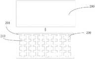
如图1至图3所示,本发明实施例中所提供的LED电路板,包括:As shown in FIG. 1 to FIG. 3 , the LED circuit board provided in the embodiment of the present invention includes:
主板100;
印刷电路板,所述印刷电路板包括电路板主体及设置在所述电路板主体上的多个金属散热块200,多个所述金属散热块200间隔设置,在相邻的所述金属散热块200之间填充有绝缘层300,所述金属散热块200包括相对设置的第一表面和第二表面,所述金属散热块200的第一表面与所述主板100连接;A printed circuit board, the printed circuit board includes a circuit board main body and a plurality of metal heat dissipation blocks 200 arranged on the circuit board main body, a plurality of the metal heat dissipation blocks 200 are arranged at intervals, and the adjacent metal heat dissipation blocks An insulating
以及,多个LED芯片400,连接在所述金属散热块200的第二表面上。And, a plurality of
本发明所提供的LED电路板,在印刷电路板上设置有相互绝缘的多个金属散热块200,LED芯片400通过金属散热块200直接连在主板100上,通过金属散热块200实现主板100与LED芯片400的导通,而无需打金线焊接或者FPC连接,金属散热块200一方面起到传输信号的作用,另一方面可以将LED芯片400产生的热量及时导出,使得LED灯的结温低于额定温度,确保LED灯正常工作,满足多个高功率LED灯的散热需求,延长使用使命。The LED circuit board provided by the present invention is provided with a plurality of metal heat dissipation blocks 200 insulated from each other on the printed circuit board. The LED chips 400 are directly connected to the
需要说明的是,在本发明所提供的LED电路板中,所述金属散热块200优选为铜块,因铜的导热性高达390w/mk,使LED器件产生的热量可迅速通过厚铜块导出,均为的分散在厚铜中并散出,进而降低LED芯片400的结点温度,满足多个大功率LED灯的散热需求。当然可以理解的是,所述金属散热块200也并不仅局限于铜块。It should be noted that, in the LED circuit board provided by the present invention, the metal
以下说明本发明所提供的LED电路板的两种优选实施例。Two preferred embodiments of the LED circuit board provided by the present invention are described below.
实施例1Example 1
图1所示为本发明所提供的LED电路板的第一种实施例的结构示意图。FIG. 1 is a schematic structural diagram of a first embodiment of the LED circuit board provided by the present invention.
在本实施例中,所述电路板主体与所述多个金属散热块200对应设置有多个开口区,所述金属散热块200嵌入在对应的所述开口区内,并与所述开口区的边缘之间具有间隙,在所述金属散热块200和所述开口区的边缘之间的间隙填充有所述绝缘层300,且所述金属散热块200的第一表面和第二表面暴露出所述电路板主体外。In this embodiment, the circuit board body and the plurality of metal heat dissipation blocks 200 are correspondingly provided with a plurality of opening areas, the metal heat dissipation blocks 200 are embedded in the corresponding opening areas, and are connected with the opening areas. There is a gap between the edges of the metal
采用上述方案,可以是通过将金属基板制作成网格状的多个金属散热块200,在不同网格内的金属散热块200之间填充绝缘层300树脂,起到分离网格和粘结作用;所述印刷电路板的电路板主体上具有多个开口区,所述金属散热块200嵌入在对应的开口区内,并通过绝缘层300来将金属散热块200与所述印刷电路板绝缘,从而实现将金属散热块200集成在印刷电路板上。With the above solution, the metal substrate can be made into a plurality of grid-shaped metal heat sink blocks 200, and the insulating
在本实施例中,优选的,所述印刷电路板在所述金属散热块200的第一表面所在一侧包括用于与所述主板100进行连接的第一焊接区域,所述印刷电路板的第一焊接区域与所述主板100之间设有用于连接所述金属散热块200与所述主板100的第一焊接材料层800。In this embodiment, preferably, the printed circuit board includes a first welding area for connecting with the
采用上述方案,所述金属散热块200的第一表面可以是通过焊接方式与所述主板100进行连接,具体地,可以采用以下方式:在主板100上对应第一焊接区域的区域印锡膏,利用SMT工艺将金属散热块200的第一表面直接焊接在主板100上。With the above solution, the first surface of the metal
在本实施例中,优选的,如图1所示,所述印刷电路板在所述金属散热块200的第一表面所在一侧还包括除所述第一焊接区域之外的第一非焊接区域,在所述金属散热块200的第一表面的第一非焊接区域与所述主板100之间设有第一阻焊层600。In this embodiment, preferably, as shown in FIG. 1 , the printed circuit board further includes a first non-soldering area in addition to the first soldering area on the side where the first surface of the
采用上述方案,在所述印刷电路板的所述金属散热块200的第一表面所在一侧,不需要焊接的区域设置第一阻焊层600,以在制作该LED电路板的过程中,起到限定出需要焊接主板100的第一焊接区域的目的。With the above solution, the first solder resist
该第一阻焊层600优选可以采用白色高反射油墨形成,优选的,可以是在金属散热块200的第一表面所在一侧整体制作阻焊层,并在该阻焊层的需要与主板100焊接连接的位置做阻焊开窗露出金属散热块200,并在主板100上印锡膏,通过SMT工艺将金属散热块200与主板100进行焊接,以将印刷电路板焊接在主板100上。The first solder resist
在本实施例中,优选的,如图1所示,所述金属散热块200的第二表面包括用于与所述LED芯片400进行连接的第二焊接区域,所述金属散热块200的第二表面的第二焊接区域与所述LED芯片400之间设有用于连接所述金属散热块200与所述主板100的第二焊接材料层700。In this embodiment, preferably, as shown in FIG. 1 , the second surface of the metal
采用上述方案,所述金属散热块200的第二表面可以是通过焊接方式与所述LED芯片400进行连接,具体地,可以采用以下方式:在印刷电路板上对应第二焊接区域的区域印锡膏,利用SMT工艺将LED芯片400直接焊接在金属散热块200的第二表面上。With the above solution, the second surface of the metal
在本实施例中,优选的,所述金属散热块200的第二表面还包括除所述第二焊接区域之外的第二非焊接区域,在所述金属散热块200的第二表面的第二非焊接区域与所述LED芯片400之间设有第二阻焊层500。In this embodiment, preferably, the second surface of the metal
采用上述方案,在所述印刷电路板的所述金属散热块200的第二表面所在一侧,不需要焊接的区域设置第二阻焊层500,以在制作该LED电路板的过程中,起到限定出需要焊接LED芯片400的第二焊接区域的目的。With the above solution, a second solder resist
该第二阻焊层500优选可以采用白色高反射油墨形成,优选的,可以是在金属散热块200的第二表面所在一侧整体制作阻焊层,并在该阻焊层的需要焊接LED芯片400的位置做阻焊开窗露出金属散热块200,并在露出的金属散热块200的第二表面印锡膏,通过SMT工艺与LED芯片400进行焊接,以将LED芯片400焊接在金属散热块200上。The second solder resist
此外,在本实施例中,优选的,如图所示,每一所述LED芯片400包括第一电极和第二电极,其中每一所述LED芯片400对应于相邻的两块所述金属散热块200之间的间隙位置设置,且每一所述LED芯片400的第一电极和第二电极分别连接在相邻的两块所述金属散热块200上。In addition, in this embodiment, preferably, as shown in the figure, each of the LED chips 400 includes a first electrode and a second electrode, wherein each of the LED chips 400 corresponds to two adjacent pieces of the metal The space between the heat dissipation blocks 200 is set, and the first electrode and the second electrode of each
本实施例所提供的LED电路板工艺简单,散热效果好,可实现将散热印刷电路板直接焊接在主板100上。The LED circuit board provided in this embodiment has a simple process and a good heat dissipation effect, and can realize the direct welding of the heat dissipation printed circuit board on the
但是,由于本实施例中,金属散热块200是通过将金属基板制作成不同的网格来形成的,因工艺能力问题,相邻的金属散热块200之间的间距难以制作在0.2mm以下,因此,实施例1所提供的LED电路板无法满足LED器件间距小于0.2mm的小型LED器件。However, in this embodiment, the
实施例2Example 2
图2所示为本发明所提供的LED电路板的第二种实施例的结构示意图。FIG. 2 is a schematic structural diagram of a second embodiment of the LED circuit board provided by the present invention.
在本实施例中,所述电路板主体与所述多个金属散热块200对应设置有多个开口区,所述金属散热块200嵌入在对应的所述开口区内,并与所述开口区的边缘之间具有间隙,在所述金属散热块200和所述开口区的边缘之间的间隙填充有所述绝缘层300,且所述金属散热块200的第一表面和第二表面暴露出所述电路板主体外。In this embodiment, the circuit board body and the plurality of metal heat dissipation blocks 200 are correspondingly provided with a plurality of opening areas, the metal heat dissipation blocks 200 are embedded in the corresponding opening areas, and are connected with the opening areas. There is a gap between the edges of the metal
采用上述方案,可以是通过将金属板制作成不同的网格,形成多个金属散热块200,在不同网格的金属散热块200中填充绝缘层300树脂,起到分离网格和粘结作用;所述印刷电路板的电路板主体上具有多个开口区,所述金属散热块200嵌入在对应的开口区内,并通过绝缘层300来将金属散热块200与所述印刷电路板绝缘,从而实现将金属散热块200集成在印刷电路板上。With the above solution, a plurality of metal heat dissipation blocks 200 can be formed by making metal plates into different grids, and the insulating
在本实施例中,优选的,在所述金属散热块200的第一表面和第二表面分别覆盖有镀金属层900,所述镀金属层900在与相邻两个所述金属散热块200之间的间隙所正对的位置设置有开口,且所述镀金属层900至少完全覆盖住所述金属散热块200,并至少覆盖住部分所述绝缘层300;所述主板100与所述金属散热块200的第一表面之间以及所述LED芯片400与所述金属散热块200之间分别通过所述镀金属层900连接。In this embodiment, preferably, the first surface and the second surface of the metal
其中,所述印刷电路板在所述金属散热块200的第一表面所在一侧包括用于与所述主板100进行连接的第一焊接区域,所述印刷电路板的第一焊接区域与所述主板100之间设有用于连接所述镀金属层900与所述主板100的第一焊接材料层800;Wherein, the printed circuit board includes a first welding area on the side where the first surface of the metal
所述印刷电路板在所述金属散热块200的第一表面所在一侧还包括除所述第一焊接区域之外的第一非焊接区域,在所述第一非焊接区域的镀金属层900与所述主板100之间设有第一阻焊层600;The printed circuit board further includes a first non-soldering area on the side where the first surface of the metal
所述印刷电路板在所述金属散热块200的第二表面所在一侧包括用于与所述LED芯片400进行连接的第二焊接区域,所述印刷电路板的第二焊接区域与所述LED芯片400之间设有用于连接所述镀金属层900与所述LED芯片400的第二焊接材料层700;The printed circuit board includes a second welding area for connecting with the
所述印刷电路板在所述金属散热块200的第二表面所在一侧还包括除所述第二焊接区域之外的第二非焊接区域,在所述第二非焊接区域的镀金属层900与所述LED芯片400之间设有第二阻焊层500。The printed circuit board further includes a second non-soldering area on the side where the second surface of the metal
采用上述方案,本发明所提供的实施例2与实施例1的区别在于,在所述金属散热块200的第一表面和第二表面上分别增加设置镀金属层900,该镀金属层900至少完全覆盖住所述金属散热块200,并能够至少覆盖一部分的绝缘层300,也就是说,该镀金属层900上的开口尺寸小于相邻两个金属散热块200之间的间隙,从而与实施例1相比,本实施例1中所提供的LED电路板通过该镀金属层900来连接LED芯片400和主板100时,可以实现组装LED器件间距小于0.2mm的小型LED器件;与实施例1相比的缺点在于,制作工艺流程上,增加了一次沉积电镀和图像蚀刻工艺。With the above solution, the difference between Embodiment 2 provided by the present invention and Embodiment 1 is that a metal plated
需要说明的是,所述镀金属层900可以是镀铜金属层,当然可以理解的是,该镀金属层900还可以是采用其他金属。It should be noted that the metal-plated
实施例3Example 3
图3所示为本发明所提供的LED电路板的第三种实施例的结构示意图。FIG. 3 is a schematic structural diagram of a third embodiment of the LED circuit board provided by the present invention.
在本实施例中,所述电路板主体与所述多个金属散热块200对应设置有多个开口区,所述金属散热块200嵌入在对应的所述开口区内,并与所述开口区的边缘之间具有间隙,在所述金属散热块200和所述开口区的边缘之间的间隙填充有所述绝缘层300,且所述金属散热块200的第一表面和第二表面暴露出所述电路板主体外。In this embodiment, the circuit board body and the plurality of metal heat dissipation blocks 200 are correspondingly provided with a plurality of opening areas, the metal heat dissipation blocks 200 are embedded in the corresponding opening areas, and are connected with the opening areas. There is a gap between the edges of the metal
采用上述方案,可以是通过将金属基板制作成网格状的多个金属散热块200,在不同网格内的金属散热块200之间填充绝缘层300树脂,起到分离网格和粘结作用;所述印刷电路板的电路板主体上具有多个开口区,所述金属散热块200嵌入在对应的开口区内,并通过绝缘层300来将金属散热块200与所述印刷电路板绝缘,从而实现将金属散热块200集成在印刷电路板上。With the above solution, the metal substrate can be made into a plurality of grid-shaped metal heat sink blocks 200, and the insulating
在本实施例中,优选的,所述印刷电路板在所述金属散热块200的第一表面所在一侧包括用于与所述主板100进行连接的第一焊接区域,所述印刷电路板的第一焊接区域与所述主板100之间设有用于连接所述金属散热块200与所述主板100的第一焊接材料层800。In this embodiment, preferably, the printed circuit board includes a first welding area for connecting with the
采用上述方案,所述金属散热块200的第一表面可以是通过焊接方式与所述主板100进行连接,具体地,可以采用以下方式:在主板100上对应第一焊接区域的区域印锡膏,利用SMT工艺将金属散热块200的第一表面直接焊接在主板100上。With the above solution, the first surface of the metal
在本实施例中,优选的,如图3所示,所述印刷电路板在所述金属散热块200的第一表面所在一侧还包括除所述第一焊接区域之外的第一非焊接区域,在所述金属散热块200的第一表面的第一非焊接区域与所述主板100之间设有第一阻焊层600。In this embodiment, preferably, as shown in FIG. 3 , the printed circuit board further includes a first non-soldering area other than the first soldering area on the side where the first surface of the
采用上述方案,在所述印刷电路板的所述金属散热块200的第一表面所在一侧,不需要焊接的区域设置第一阻焊层600,以在制作该LED电路板的过程中,起到限定出需要焊接主板100的第一焊接区域的目的。With the above solution, the first solder resist
该第一阻焊层600优选可以采用白色高反射油墨形成,优选的,可以是在金属散热块200的第一表面所在一侧整体制作阻焊层,并在该阻焊层的需要与主板100焊接连接的位置做阻焊开窗露出金属散热块200,并在主板100上印锡膏,通过SMT工艺将金属散热块200与主板100进行焊接,以将印刷电路板焊接在主板100上。The first solder resist
在本实施例中,优选的,如图3所示,所述金属散热块200的第二表面包括用于与所述LED芯片400进行连接的第二焊接区域,所述金属散热块200的第二表面的第二焊接区域与所述LED芯片400之间设有用于连接所述金属散热块200与所述主板100的第二焊接材料层700。In this embodiment, preferably, as shown in FIG. 3 , the second surface of the metal
采用上述方案,所述金属散热块200的第二表面可以是通过焊接方式与所述LED芯片400进行连接,具体地,可以采用以下方式:在印刷电路板上对应第二焊接区域的区域印锡膏,利用SMT工艺将LED芯片400直接焊接在金属散热块200的第二表面上。With the above solution, the second surface of the metal
在本实施例中,优选的,所述金属散热块200的第二表面还包括除所述第二焊接区域之外的第二非焊接区域,在所述金属散热块200的第二表面的第二非焊接区域与所述LED芯片400之间设有第二阻焊层500。In this embodiment, preferably, the second surface of the metal
采用上述方案,在所述印刷电路板的所述金属散热块200的第二表面所在一侧,不需要焊接的区域设置第二阻焊层500,以在制作该LED电路板的过程中,起到限定出需要焊接LED芯片400的第二焊接区域的目的。With the above solution, a second solder resist
该第二阻焊层500优选可以采用白色高反射油墨形成,优选的,可以是在金属散热块200的第二表面所在一侧整体制作阻焊层,并在该阻焊层的需要焊接LED芯片400的位置做阻焊开窗露出金属散热块200,并在露出的金属散热块200的第二表面印锡膏,通过SMT工艺与LED芯片400进行焊接,以将LED芯片400焊接在金属散热块200上。The second solder resist
此外,在本实施例中,优选的,如图3所示,每一所述LED芯片400包括第一电极和第二电极,其中每一所述LED芯片400对应于相邻的两块所述金属散热块200之间的间隙位置设置,且每一所述LED芯片400的第一电极和第二电极分别连接在相邻的两块所述金属散热块200上。In addition, in this embodiment, preferably, as shown in FIG. 3 , each of the LED chips 400 includes a first electrode and a second electrode, wherein each of the LED chips 400 corresponds to two adjacent pieces of the LED chips 400 . The position of the gap between the metal heat dissipation blocks 200 is set, and the first electrode and the second electrode of each of the
本实施例所提供的LED电路板工艺简单,散热效果好,可实现将散热印刷电路板直接焊接在主板100上。The LED circuit board provided in this embodiment has a simple process and a good heat dissipation effect, and can realize the direct welding of the heat dissipation printed circuit board on the
本实施例与实施例1所不同的是,如图3所示,相邻的所述金属散热块之间的间隙包括靠近所述金属散热块的第一表面的第一端和靠近所述金属散热块的第二表面的第二端,其中所述间隙的第一端的尺寸大于所述间隙的第二端的尺寸。The difference between this embodiment and Embodiment 1 is that, as shown in FIG. 3 , the gap between the adjacent metal heat dissipation blocks includes a first end close to the first surface of the metal heat dissipation block and a first end close to the metal heat dissipation block. The second end of the second surface of the heat sink, wherein the size of the first end of the gap is greater than the size of the second end of the gap.
采用上述方案,相邻的金属散热块之间的间隙在靠近主板的一端(即所述间隙的第二端)的间距较大,而在靠近LED芯片的一端(即所述间隙的第一端)的间距比较小,可以适合小间距器件的贴片。With the above solution, the gaps between adjacent metal heat sinks are larger at one end close to the main board (ie the second end of the gap), while at the end close to the LED chip (ie the first end of the gap) ) pitch is relatively small, which can be suitable for the patch of small-pitch devices.
在本发明的实施例中还提供了一种终端设备,包括本发明实施例中所提供的LED电路板。An embodiment of the present invention also provides a terminal device, including the LED circuit board provided in the embodiment of the present invention.
本发明实施例中还提供了一种LED电路板的制作方法,所述方法包括:An embodiment of the present invention also provides a method for manufacturing an LED circuit board, the method comprising:
提供一主板100;providing a
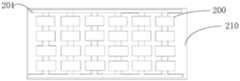
制作印刷电路板,所述印刷电路板包括电路板主体210及设置在所述电路板主体210上的多个金属散热块200,多个所述金属散热块200间隔设置,在相邻的所述金属散热块200之间填充有绝缘层300,所述金属散热块200包括相对的第一表面和第二表面;A printed circuit board is produced. The printed circuit board includes a circuit board
将所述金属散热块200的第一表面与所述主板100连接;connecting the first surface of the metal
将LED芯片400连接在所述金属散热块200的第二表面上。The
下分别说明本发明所提供的LED电路板的两种制作方法。The two manufacturing methods of the LED circuit board provided by the present invention are respectively described below.
实施例1:Example 1:
本实施例所提供的LED电路板的制作方法用于制作本发明第一种实施例中所提供的LED电路板,所述方法具体包括:The manufacturing method of the LED circuit board provided in this embodiment is used to manufacture the LED circuit board provided in the first embodiment of the present invention, and the method specifically includes:
提供一主板100;providing a
制作印刷电路板,所述印刷电路板包括电路板主体210及设置在所述电路板主体210上的多个金属散热块200,多个所述金属散热块200间隔设置,在相邻的所述金属散热块200之间填充有绝缘层300,所述金属散热块200包括相对的第一表面和第二表面;A printed circuit board is produced. The printed circuit board includes a circuit board
将所述金属散热块200的第一表面与所述主板100连接;connecting the first surface of the metal
将LED芯片400连接在所述金属散热块200的第二表面上。The
其中,在本实施例中,所述制作印刷电路板,具体包括:Wherein, in this embodiment, the manufacturing of the printed circuit board specifically includes:
如图4所示,提供一印刷电路板基板211,在所述印刷电路板基板211上开槽,形成多个开口区212,以制作得到所述电路板主体210;As shown in FIG. 4 , a printed
如图5所示,提供一金属基板220,并在所述金属基板220上捞型出与多个开口区212对应的金属散热块200,且相邻的金属散热块200之间通过连接筋213连接为一体;As shown in FIG. 5 , a metal substrate 220 is provided, and the metal heat dissipation blocks 200 corresponding to the plurality of opening
如图6所示,将所述金属基板220上的各金属散热块200放入所述电路板主体210上对应的开口区212内,将所述金属基板220与所述电路板主体210进行压合;As shown in FIG. 6 , each
将所述压合好的金属基板220和所述电路板主体210进行磨板处理,以使得所述金属散热块200的第一表面和第二表面暴露出所述电路板主体210外;grinding the pressed metal substrate 220 and the circuit board
如图7所示,将相邻的金属散热块200之间的连接筋213去除;As shown in FIG. 7 , the connecting
如图8所示,在相邻的金属散热块200以及所述金属散热块200与所述开口区的边缘之间填充绝缘层300树脂,以形成所述绝缘层300。As shown in FIG. 8 , an insulating
在上述方案中,制作形成所述印刷电路板的步骤中,具体地,In the above solution, in the step of manufacturing and forming the printed circuit board, specifically,
如图5所示,所述金属基板220可以是采用机械的方式捞型出多个网格状的金属散热块200,相邻的金属散热块200之间用1-5mm的连接筋213连接,在多个网格状的金属散热块200上还连接有工艺边金属块201;As shown in FIG. 5 , the metal substrate 220 can be mechanically drawn out of a plurality of grid-shaped metal heat dissipation blocks 200, and adjacent metal heat dissipation blocks 200 are connected by connecting
所述电路板主体210是将整块的PCB基板用机械的方式开槽,形成具有多个开口区的电路板主体210,其中该电路板主体210上的开口区212中,需要金属散热块200的开槽尺寸要比金属散热块200的尺寸大2-5mil,对需埋入工艺边金属块201的开口区212的开槽尺寸比工艺边铜块的尺寸大1mil内;The circuit board
如图6所示,将具有开口区212的电路板主体210与网格状的金属散热块200预叠组合时,通过压合的方式将金属散热块200与电路板主体210压合一起,并用绝缘层300树脂粘结;压合后进行磨板处理,露出金属散热块200;再将连接金属散热块200的连接筋213去除,并在连接筋213捞空区域塞绝缘层300树脂,形成具有埋入金属散热块200的印刷电路板母板,再将该母板制作形成印刷电路板。As shown in FIG. 6 , when the circuit board
其中,需要说明的是,在本实施例中,如图7所示,将相邻的金属散热块之间的连接筋去除,具体可以采用以下方式:利用机械捞型或者机械钻或者图形蚀刻的方式将连接筋直接全部去除。It should be noted that, in this embodiment, as shown in FIG. 7 , to remove the connecting ribs between adjacent metal heat sinks, the following methods can be used: using a mechanical fishing type or a mechanical drill or pattern etching way to remove all the connecting ribs directly.
在本实施例中,所述将所述金属散热块200的第一表面与所述主板100连接,具体包括:In this embodiment, connecting the first surface of the metal
在所述金属散热块200的第一表面制作第一阻焊层600,并在所述第一阻焊层600上对应所述第一焊接区域的位置开口,以暴露出所述金属散热块200的第一表面;A first solder resist
在第一阻焊层600上暴露出所述金属散热块200的第一表面的位置采用焊接方式连接所述LED芯片400。The position where the first surface of the metal
在上述方案中,所述第一阻焊层600可以是通过在金属散热块200的第一表面所在一侧制作白色高反射油墨层而形成,并在该第一阻焊层600的需要焊接主板100的位置做阻焊开窗露出金属散热块200,然后在主板100上印锡膏,利用SMT工艺将印刷电路板焊接在主板100上。In the above solution, the first solder resist
此外,在本实施例中,所述将所述金属散热块200的第二表面与所述主板100连接,具体包括:In addition, in this embodiment, the connecting the second surface of the metal
在所述金属散热块200的第二表面制作第二阻焊层500,并在所述第二阻焊层500上对应所述第二焊接区域的位置开口,以暴露出所述金属散热块200的第二表面;A second solder resist
在第二阻焊层500上暴露出所述金属散热块200的第二表面的位置采用焊接方式连接所述LED芯片400。The position where the second surface of the metal
在上述方案中,所述第二阻焊层500可以是通过在金属散热块200的第二表面所在一侧制作白色高反射油墨层而形成,并在该第二阻焊层500的需要焊接LED芯片400的位置做阻焊开窗露出金属散热块200,然后在第二阻焊层500上开窗露出金属散热块200的位置印锡膏,利用SMT工艺将LED芯片400焊接在金属散热块200上。In the above solution, the second solder resist
本实施例所提供的LED制作方法工艺简单,可将5mm以下的金属散热块埋入到印刷电路板中,可在每个所需散热的器件下埋入小金属散热块,散热效果好,且适合于批量生产。The LED manufacturing method provided in this embodiment has a simple process, and can embed a metal heat dissipation block below 5 mm in the printed circuit board, and can embed a small metal heat dissipation block under each device that needs to be dissipated. The heat dissipation effect is good, and Suitable for mass production.
但是,本实施例所提供的LED制作方法,去除连接筋受现有工艺能力的限制,难以满足金属散热块间距在0.25mm以下的印刷电路板生产。However, in the LED manufacturing method provided in this embodiment, the removal of connecting ribs is limited by the existing process capability, and it is difficult to meet the production of printed circuit boards with a metal heat dissipation block pitch of less than 0.25 mm.
实施例2Example 2
本实施例所提供的LED电路板的制作方法用于制作本发明第二种实施例中所提供的LED电路板,所述方法具体包括:The manufacturing method of the LED circuit board provided in this embodiment is used to manufacture the LED circuit board provided in the second embodiment of the present invention, and the method specifically includes:
提供一主板100;providing a
制作印刷电路板,所述印刷电路板包括电路板主体210及设置在所述电路板主体210上的多个金属散热块200,多个所述金属散热块200间隔设置,在相邻的所述金属散热块200之间填充有绝缘层300,所述金属散热块200包括相对的第一表面和第二表面;A printed circuit board is produced. The printed circuit board includes a circuit board
将所述金属散热块200的第一表面与所述主板100连接;connecting the first surface of the metal
将LED芯片400连接在所述金属散热块200的第二表面上。The
其中,在本实施例中,所述制作印刷电路板,具体包括:Wherein, in this embodiment, the manufacturing of the printed circuit board specifically includes:
如图4所示,提供一印刷电路板基板,在所述印刷电路板基板上开槽,形成多个开口区212,以制作得到所述电路板主体210;As shown in FIG. 4 , a printed circuit board substrate is provided, and grooves are formed on the printed circuit board substrate to form a plurality of opening
如图5所示,提供一金属基板220,并在所述金属基板220上捞型出与多个开口区212对应的金属散热块200,且相邻的金属散热块200之间通过连接筋213连接为一体;As shown in FIG. 5 , a metal substrate 220 is provided, and the metal heat dissipation blocks 200 corresponding to the plurality of opening
如图6所示,将所述金属基板220上的各金属散热块200放入所述电路板主体210上对应的开口区212内,将所述金属基板220与所述电路板主体210进行压合;As shown in FIG. 6 , each
将所述压合好的金属基板220和所述电路板主体210进行磨板处理,以使得所述金属散热块200的第一表面和第二表面暴露出所述电路板主体210外;grinding the pressed metal substrate 220 and the circuit board
如图7所示,将相邻的金属散热块200之间的连接筋213去除;As shown in FIG. 7 , the connecting
如图8所示,在相邻的金属散热块200以及所述金属散热块200与所述开口区212的边缘之间填充绝缘层300树脂,以形成所述绝缘层300。As shown in FIG. 8 , resin of the insulating
在本实施例中,与实施例1不同的是,在所述方法中,所述制作印刷电路板具体还包括:In this embodiment, different from Embodiment 1, in the method, the manufacturing of the printed circuit board further includes:
在所述金属散热块200的第一表面和第二表面分别整面镀上镀金属层900,并在所述镀金属层900的与相邻两个所述金属散热块200之间的间隙所正对的位置刻蚀出开口,且使得所述镀金属层900至少完全覆盖住所述金属散热块200,并至少覆盖住部分所述绝缘层300。The first surface and the second surface of the metal
在上述方案中,在金属散热块200的第一表面和第二表面进行整板沉铜电镀,在绝缘层300树脂和金属散热块200上镀金属层900,然后利用图形蚀刻工艺将加镀上的图局部蚀刻,制作出不同的网格图形。In the above scheme, the first surface and the second surface of the metal
在本实施例中,制作形成所述印刷电路板的步骤中,具体地,In this embodiment, in the step of manufacturing and forming the printed circuit board, specifically,
所述金属基板220可以是采用机械的方式捞型出多个网格状的金属散热块200,相邻的金属散热块200之间用1-5mm的连接筋213连接,在多个网格状的金属散热块200上还连接有工艺边金属块201;The metal substrate 220 may be a plurality of mesh-shaped
所述电路板主体210是将整块的PCB基板用机械的方式开槽,形成具有多个开口区212的电路板主体210,其中该电路板主体210上的开口区212中,需要金属散热块200的开槽尺寸要比金属散热块200的尺寸大2-5mil,对需埋入工艺边金属块201的开口区212的开槽尺寸比工艺边铜块的尺寸大1mil内;The circuit board
将具有开口区212的电路板主体210与网格状的金属散热块200预叠组合时,通过压合的方式将金属散热块200与电路板主体210压合一起,并用绝缘层300树脂粘结;压合后进行磨板处理,露出金属散热块200;再利用机械捞型或者机械钻或者图形蚀刻的方式将连接金属散热块200的连接筋213去除,并在连接筋213捞空区域塞绝缘层300树脂,形成具有埋入金属散热块200的印刷电路板母板,再将该母板制作形成印刷电路板。When the circuit board
在本实施例中,所述将所述金属散热块200的第一表面与所述主板100连接,具体包括:In this embodiment, connecting the first surface of the metal
在所述印刷电路板上、所述金属散热块200的第一表面所在一侧制作第一阻焊层600,并在所述第一阻焊层600上对应所述第一焊接区域的位置开口,以暴露出位于所述金属散热块200的第一表面上的所述镀金属层900;A first solder resist
在第一阻焊层600上暴露出所述镀金属层900的位置采用焊接方式连接所述LED芯片400。The
在上述方案中,所述第一阻焊层600可以是通过在金属散热块200的第一表面所在一侧的镀金属层900上制作白色高反射油墨层而形成,并在该第一阻焊层600的需要焊接主板100的位置做阻焊开窗露出镀金属层900,然后在主板100上印锡膏,利用SMT工艺将镀金属层900焊接在主板100上,实现主板100与金属散热块200连接。In the above solution, the first solder resist
此外,在本实施例中,所述将所述金属散热块200的第二表面与所述主板100连接,具体包括:In addition, in this embodiment, the connecting the second surface of the metal
在所述印刷电路板上、所述金属散热块200的第二表面所在一侧制作第二阻焊层500,并在所述第二阻焊层500上对应所述第二焊接区域的位置开口,以暴露出位于所述金属散热块200的第二表面上的镀金属层900;A second solder resist
在第二阻焊层500上暴露出所述镀金属层900的位置采用焊接方式连接所述LED芯片400。The
在上述方案中,所述第二阻焊层500可以是通过在金属散热块200的第二表面所在一侧的镀金属层900上制作白色高反射油墨层而形成,并在该第二阻焊层500的需要焊接LED芯片400的位置做阻焊开窗露出镀金属层900,然后在第二阻焊层500上开窗露出镀金属层900的位置印锡膏,利用SMT工艺将LED芯片400焊接在镀金属层900上,进而实现LED芯片400与所述金属散热块200连接。In the above solution, the second solder resist
本实施例所提供的LED电路板制作方法,与实施例1的制作方法区别在于,在所述金属散热块200的第一表面和第二表面上分别增加设置镀金属层900,该镀金属层900至少完全覆盖住所述金属散热块200,并能够至少覆盖一部分的绝缘层300,也就是说,该镀金属层900上的开口尺寸小于相邻两个金属散热块200之间的间隙,从而与实施例1相比,本实施例1中所提供的LED电路板通过该镀金属层900来连接LED芯片400和主板100时,可以实现组装LED器件间距小于0.2mm的小型LED器件;与实施例1相比的缺点在于,制作工艺流程上,增加了一次沉积电镀和图像蚀刻工艺。The difference between the manufacturing method of the LED circuit board provided in this embodiment and the manufacturing method of Embodiment 1 is that a metal plated
实施例3Example 3
本实施例所提供的LED电路板的制作方法用于制作本发明第一种实施例中所提供的LED电路板,所述方法具体包括:The manufacturing method of the LED circuit board provided in this embodiment is used to manufacture the LED circuit board provided in the first embodiment of the present invention, and the method specifically includes:
提供一主板100;providing a
制作印刷电路板,所述印刷电路板包括电路板主体210及设置在所述电路板主体210上的多个金属散热块200,多个所述金属散热块200间隔设置,在相邻的所述金属散热块200之间填充有绝缘层300,所述金属散热块200包括相对的第一表面和第二表面;A printed circuit board is produced. The printed circuit board includes a circuit board
将所述金属散热块200的第一表面与所述主板100连接;connecting the first surface of the metal
将LED芯片400连接在所述金属散热块200的第二表面上。The
其中,在本实施例中,所述制作印刷电路板,具体包括:Wherein, in this embodiment, the manufacturing of the printed circuit board specifically includes:
如图4所示,提供一印刷电路板基板211,在所述印刷电路板基板211上开槽,形成多个开口区212,以制作得到所述电路板主体210;As shown in FIG. 4 , a printed
如图5所示,提供一金属基板220,并在所述金属基板220上捞型出与多个开口区212对应的金属散热块200,且相邻的金属散热块200之间通过连接筋213连接为一体;As shown in FIG. 5 , a metal substrate 220 is provided, and the metal heat dissipation blocks 200 corresponding to the plurality of opening
如图6所示,将所述金属基板220上的各金属散热块200放入所述电路板主体210上对应的开口区212内,将所述金属基板220与所述电路板主体210进行压合;As shown in FIG. 6 , each
将所述压合好的金属基板220和所述电路板主体210进行磨板处理,以使得所述金属散热块200的第一表面和第二表面暴露出所述电路板主体210外;grinding the pressed metal substrate 220 and the circuit board
如图7所示,将相邻的金属散热块200之间的连接筋213去除;As shown in FIG. 7 , the connecting
如图8所示,在相邻的金属散热块200以及所述金属散热块200与所述开口区的边缘之间填充绝缘层300树脂,以形成所述绝缘层300。As shown in FIG. 8 , an insulating
在上述方案中,制作形成所述印刷电路板的步骤中,具体地,In the above solution, in the step of manufacturing and forming the printed circuit board, specifically,
所述金属基板220可以是采用机械的方式捞型出多个网格状的金属散热块200,相邻的金属散热块200之间用1-5mm的连接筋213连接,在多个网格状的金属散热块200上还连接有工艺边金属块201;The metal substrate 220 may be a plurality of mesh-shaped
所述电路板主体210是将整块的PCB基板用机械的方式开槽,形成具有多个开口区的电路板主体210,其中该电路板主体210上的开口区212中,需要金属散热块200的开槽尺寸要比金属散热块200的尺寸大2-5mil,对需埋入工艺边金属块201的开口区212的开槽尺寸比工艺边铜块的尺寸大1mil内;The circuit board
将具有开口区212的电路板主体210与网格状的金属散热块200预叠组合时,通过压合的方式将金属散热块200与电路板主体210压合一起,并用绝缘层300树脂粘结;压合后进行磨板处理,露出金属散热块200;再将连接金属散热块200的连接筋213去除,并在连接筋213捞空区域塞绝缘层300树脂,形成具有埋入金属散热块200的印刷电路板母板,再将该母板制作形成印刷电路板。When the circuit board
在本实施例中,所述将所述金属散热块200的第一表面与所述主板100连接,具体包括:In this embodiment, connecting the first surface of the metal
在所述金属散热块200的第一表面制作第一阻焊层600,并在所述第一阻焊层600上对应所述第一焊接区域的位置开口,以暴露出所述金属散热块200的第一表面;A first solder resist
在第一阻焊层600上暴露出所述金属散热块200的第一表面的位置采用焊接方式连接所述LED芯片400。The position where the first surface of the metal
在上述方案中,所述第一阻焊层600可以是通过在金属散热块200的第一表面所在一侧制作白色高反射油墨层而形成,并在该第一阻焊层600的需要焊接主板100的位置做阻焊开窗露出金属散热块200,然后在主板100上印锡膏,利用SMT工艺将印刷电路板焊接在主板100上。In the above solution, the first solder resist
此外,在本实施例中,所述将所述金属散热块200的第二表面与所述主板100连接,具体包括:In addition, in this embodiment, the connecting the second surface of the metal
在所述金属散热块200的第二表面制作第二阻焊层500,并在所述第二阻焊层500上对应所述第二焊接区域的位置开口,以暴露出所述金属散热块200的第二表面;A second solder resist
在第二阻焊层500上暴露出所述金属散热块200的第二表面的位置采用焊接方式连接所述LED芯片400。The position where the second surface of the metal
在上述方案中,所述第二阻焊层500可以是通过在金属散热块200的第二表面所在一侧制作白色高反射油墨层而形成,并在该第二阻焊层500的需要焊接LED芯片400的位置做阻焊开窗露出金属散热块200,然后在第二阻焊层500上开窗露出金属散热块200的位置印锡膏,利用SMT工艺将LED芯片400焊接在金属散热块200上。In the above solution, the second solder resist
本实施例所提供的LED制作方法工艺简单,可将5mm以下的金属散热块埋入到印刷电路板中,可在每个所需散热的器件下埋入小金属散热块,散热效果好,且适合于批量生产。The LED manufacturing method provided in this embodiment has a simple process, and can embed a metal heat dissipation block below 5 mm in the printed circuit board, and can embed a small metal heat dissipation block under each device that needs to be dissipated. The heat dissipation effect is good, and Suitable for mass production.
其中,需要说明的是,在本实施例中,与实施例1相比,不同之处在于,将相邻的金属散热块之间的连接筋去除,具体可以采用以下方式:利用机械控深铣或孔深钻或V-CUT方式在金属散热块的第二表面去除连接筋的大部分,连接筋的剩余部分优选的管控在50μm以内,然后,再利用图形转移工艺,在金属散热块的第一表面利用图形蚀刻方式将剩余的连接筋蚀刻掉,此蚀刻间距可按LED器件间距设计,满足0.2mm以下间距器件的贴片需求,以使得相邻的所述金属散热块之间的间隙在靠近所述金属散热块的第一表面的第一端的尺寸大于靠近所述金属散热块的第二表面的第二端的尺寸。It should be noted that, in this embodiment, compared with Embodiment 1, the difference is that the connecting ribs between adjacent metal heat sinks are removed. Specifically, the following methods can be used: using mechanically controlled deep milling Or deep drilling or V-CUT method to remove most of the connecting rib on the second surface of the metal heat sink, the remaining part of the connecting rib is preferably controlled within 50μm, and then, using the pattern transfer process, on the second surface of the metal heat sink. The remaining connecting ribs are etched on one surface by pattern etching. The etching spacing can be designed according to the LED device spacing to meet the patch requirements of devices with a spacing of less than 0.2mm, so that the gap between the adjacent metal heat sinks is The size of the first end near the first surface of the metal heat sink is greater than the size of the second end near the second surface of the metal heat block.
以上所述仅是本发明的优选实施方式,应当指出,对于本技术领域的普通技术人员来说,在不脱离本发明技术原理的前提下,还可以做出若干改进和替换,这些改进和替换也应视为本发明的保护范围。The above are only the preferred embodiments of the present invention. It should be pointed out that for those skilled in the art, without departing from the technical principle of the present invention, several improvements and replacements can be made. These improvements and replacements It should also be regarded as the protection scope of the present invention.
Claims (15)
Priority Applications (1)
| Application Number | Priority Date | Filing Date | Title |
|---|---|---|---|
| CN201710630373.0ACN107331659B (en) | 2017-07-28 | 2017-07-28 | LED circuit board, terminal equipment and manufacturing method of LED circuit board |
Applications Claiming Priority (1)
| Application Number | Priority Date | Filing Date | Title |
|---|---|---|---|
| CN201710630373.0ACN107331659B (en) | 2017-07-28 | 2017-07-28 | LED circuit board, terminal equipment and manufacturing method of LED circuit board |
Publications (2)
| Publication Number | Publication Date |
|---|---|
| CN107331659A CN107331659A (en) | 2017-11-07 |
| CN107331659Btrue CN107331659B (en) | 2020-03-03 |
Family
ID=60227739
Family Applications (1)
| Application Number | Title | Priority Date | Filing Date |
|---|---|---|---|
| CN201710630373.0AActiveCN107331659B (en) | 2017-07-28 | 2017-07-28 | LED circuit board, terminal equipment and manufacturing method of LED circuit board |
Country Status (1)
| Country | Link |
|---|---|
| CN (1) | CN107331659B (en) |
Families Citing this family (8)
| Publication number | Priority date | Publication date | Assignee | Title |
|---|---|---|---|---|
| CN107949174A (en)* | 2017-12-04 | 2018-04-20 | 广州兴森快捷电路科技有限公司 | The production method for burying copper billet circuit board |
| CN108347822B (en)* | 2018-01-31 | 2020-03-10 | 维沃移动通信有限公司 | Circuit board, terminal equipment and manufacturing method of circuit board |
| CN108551718B (en)* | 2018-03-14 | 2021-04-13 | 维沃移动通信有限公司 | Preparation method of heat dissipation substrate |
| CN108401371B (en)* | 2018-04-25 | 2019-11-26 | 维沃移动通信有限公司 | A kind of radiator structure processing method and radiator structure |
| CN111315108B (en)* | 2018-12-12 | 2022-06-17 | 珠海方正科技高密电子有限公司 | Circuit board and electrical equipment |
| TWI672711B (en)* | 2019-01-10 | 2019-09-21 | 健策精密工業股份有限公司 | Insulated metal substrate and manufacturing method thereof |
| CN110636690B (en)* | 2019-10-23 | 2020-12-11 | 昆山沪利微电有限公司 | Heat dissipation substrate structure and manufacturing method thereof |
| CN112888156B (en)* | 2021-01-15 | 2022-02-18 | 新余市木林森线路板有限公司 | High-thermal-conductivity aluminum-based circuit board and preparation process thereof |
Family Cites Families (3)
| Publication number | Priority date | Publication date | Assignee | Title |
|---|---|---|---|---|
| JP4864419B2 (en)* | 2005-10-28 | 2012-02-01 | 株式会社東芝 | Printed circuit boards and electronic equipment |
| TW200845877A (en)* | 2007-05-07 | 2008-11-16 | Tysun Inc | Heat-dissipating substrates of composite structure |
| CN104465552B (en)* | 2014-12-26 | 2018-05-04 | 苏州旭创科技有限公司 | Encapsulating structure and optical module |
- 2017
- 2017-07-28CNCN201710630373.0Apatent/CN107331659B/enactiveActive
Also Published As
| Publication number | Publication date |
|---|---|
| CN107331659A (en) | 2017-11-07 |
Similar Documents
| Publication | Publication Date | Title |
|---|---|---|
| CN107331659B (en) | LED circuit board, terminal equipment and manufacturing method of LED circuit board | |
| CN102544310B (en) | Mounting substrate and manufacturing method thereof | |
| CN103378014A (en) | Package carrier and method for manufacturing the same | |
| CN107896421B (en) | PCB capable of fast radiating | |
| CN103227275A (en) | Wiring substrate, light emitting device, and manufacturing method of wiring substrate | |
| CN103841750A (en) | Package carrier | |
| JPWO2006030671A1 (en) | LED device | |
| CN107896423A (en) | PCB capable of fast radiating | |
| CN107734839A (en) | a PCB | |
| CN111050459A (en) | Printed circuit board and optical module | |
| CN111132476A (en) | Preparation method of double-sided circuit heat dissipation substrate | |
| CN102790140B (en) | Packaging structure and manufacturing method thereof | |
| CN106455472A (en) | Method for manufacturing high heat radiation LED circuit board bulb module group | |
| KR101115403B1 (en) | Light emitting apparatus | |
| CN111031687A (en) | Method for preparing a heat-dissipating circuit board | |
| CN103716982A (en) | High thermal conductivity printed circuit board structure | |
| US11545412B2 (en) | Package structure and manufacturing method thereof | |
| JP6420966B2 (en) | WIRING BOARD, MANUFACTURING METHOD THEREOF, AND ELECTRONIC COMPONENT DEVICE | |
| US20120267674A1 (en) | Mounting substrate, light emitting body, and method for manufacturing mounting substrate | |
| KR20120100303A (en) | Printed circuit board, light emitting module having the same, lighting unit having the light emitting unit and method of manufacturing the light emitting mudule | |
| KR20200007299A (en) | Led heat radiation improved printed circuit board and manufacturing method thereof | |
| CN107683016A (en) | A fast heat dissipation PCB | |
| CN111642059A (en) | Heat dissipation PCB and manufacturing method thereof | |
| GB2480428A (en) | PCB with metal core having extended heatsink bosses for mounting LEDs | |
| KR100616413B1 (en) | Light emitting diodes and manufacturing method thereof |
Legal Events
| Date | Code | Title | Description |
|---|---|---|---|
| PB01 | Publication | ||
| PB01 | Publication | ||
| SE01 | Entry into force of request for substantive examination | ||
| SE01 | Entry into force of request for substantive examination | ||
| GR01 | Patent grant | ||
| GR01 | Patent grant |