CN107302061B - OLED display substrate, manufacturing method thereof and display device - Google Patents
OLED display substrate, manufacturing method thereof and display deviceDownload PDFInfo
- Publication number
- CN107302061B CN107302061BCN201710631205.3ACN201710631205ACN107302061BCN 107302061 BCN107302061 BCN 107302061BCN 201710631205 ACN201710631205 ACN 201710631205ACN 107302061 BCN107302061 BCN 107302061B
- Authority
- CN
- China
- Prior art keywords
- layer
- photoresist
- substrate
- pattern
- forming
- Prior art date
- Legal status (The legal status is an assumption and is not a legal conclusion. Google has not performed a legal analysis and makes no representation as to the accuracy of the status listed.)
- Active
Links
Images


Classifications
- G—PHYSICS
- G02—OPTICS
- G02F—OPTICAL DEVICES OR ARRANGEMENTS FOR THE CONTROL OF LIGHT BY MODIFICATION OF THE OPTICAL PROPERTIES OF THE MEDIA OF THE ELEMENTS INVOLVED THEREIN; NON-LINEAR OPTICS; FREQUENCY-CHANGING OF LIGHT; OPTICAL LOGIC ELEMENTS; OPTICAL ANALOGUE/DIGITAL CONVERTERS
- G02F1/00—Devices or arrangements for the control of the intensity, colour, phase, polarisation or direction of light arriving from an independent light source, e.g. switching, gating or modulating; Non-linear optics
- G02F1/01—Devices or arrangements for the control of the intensity, colour, phase, polarisation or direction of light arriving from an independent light source, e.g. switching, gating or modulating; Non-linear optics for the control of the intensity, phase, polarisation or colour
- G02F1/13—Devices or arrangements for the control of the intensity, colour, phase, polarisation or direction of light arriving from an independent light source, e.g. switching, gating or modulating; Non-linear optics for the control of the intensity, phase, polarisation or colour based on liquid crystals, e.g. single liquid crystal display cells
- G02F1/133—Constructional arrangements; Operation of liquid crystal cells; Circuit arrangements
- G02F1/1333—Constructional arrangements; Manufacturing methods
- G02F1/1339—Gaskets; Spacers; Sealing of cells
- G02F1/13394—Gaskets; Spacers; Sealing of cells spacers regularly patterned on the cell subtrate, e.g. walls, pillars
- H—ELECTRICITY
- H10—SEMICONDUCTOR DEVICES; ELECTRIC SOLID-STATE DEVICES NOT OTHERWISE PROVIDED FOR
- H10K—ORGANIC ELECTRIC SOLID-STATE DEVICES
- H10K59/00—Integrated devices, or assemblies of multiple devices, comprising at least one organic light-emitting element covered by group H10K50/00
- H10K59/10—OLED displays
- H10K59/12—Active-matrix OLED [AMOLED] displays
- H10K59/122—Pixel-defining structures or layers, e.g. banks
- H—ELECTRICITY
- H10—SEMICONDUCTOR DEVICES; ELECTRIC SOLID-STATE DEVICES NOT OTHERWISE PROVIDED FOR
- H10K—ORGANIC ELECTRIC SOLID-STATE DEVICES
- H10K71/00—Manufacture or treatment specially adapted for the organic devices covered by this subclass
- H—ELECTRICITY
- H10—SEMICONDUCTOR DEVICES; ELECTRIC SOLID-STATE DEVICES NOT OTHERWISE PROVIDED FOR
- H10K—ORGANIC ELECTRIC SOLID-STATE DEVICES
- H10K71/00—Manufacture or treatment specially adapted for the organic devices covered by this subclass
- H10K71/20—Changing the shape of the active layer in the devices, e.g. patterning
- H10K71/231—Changing the shape of the active layer in the devices, e.g. patterning by etching of existing layers
- H10K71/233—Changing the shape of the active layer in the devices, e.g. patterning by etching of existing layers by photolithographic etching
- G—PHYSICS
- G03—PHOTOGRAPHY; CINEMATOGRAPHY; ANALOGOUS TECHNIQUES USING WAVES OTHER THAN OPTICAL WAVES; ELECTROGRAPHY; HOLOGRAPHY
- G03F—PHOTOMECHANICAL PRODUCTION OF TEXTURED OR PATTERNED SURFACES, e.g. FOR PRINTING, FOR PROCESSING OF SEMICONDUCTOR DEVICES; MATERIALS THEREFOR; ORIGINALS THEREFOR; APPARATUS SPECIALLY ADAPTED THEREFOR
- G03F7/00—Photomechanical, e.g. photolithographic, production of textured or patterned surfaces, e.g. printing surfaces; Materials therefor, e.g. comprising photoresists; Apparatus specially adapted therefor
- G03F7/16—Coating processes; Apparatus therefor
- G—PHYSICS
- G03—PHOTOGRAPHY; CINEMATOGRAPHY; ANALOGOUS TECHNIQUES USING WAVES OTHER THAN OPTICAL WAVES; ELECTROGRAPHY; HOLOGRAPHY
- G03F—PHOTOMECHANICAL PRODUCTION OF TEXTURED OR PATTERNED SURFACES, e.g. FOR PRINTING, FOR PROCESSING OF SEMICONDUCTOR DEVICES; MATERIALS THEREFOR; ORIGINALS THEREFOR; APPARATUS SPECIALLY ADAPTED THEREFOR
- G03F7/00—Photomechanical, e.g. photolithographic, production of textured or patterned surfaces, e.g. printing surfaces; Materials therefor, e.g. comprising photoresists; Apparatus specially adapted therefor
- G03F7/20—Exposure; Apparatus therefor
- G—PHYSICS
- G03—PHOTOGRAPHY; CINEMATOGRAPHY; ANALOGOUS TECHNIQUES USING WAVES OTHER THAN OPTICAL WAVES; ELECTROGRAPHY; HOLOGRAPHY
- G03F—PHOTOMECHANICAL PRODUCTION OF TEXTURED OR PATTERNED SURFACES, e.g. FOR PRINTING, FOR PROCESSING OF SEMICONDUCTOR DEVICES; MATERIALS THEREFOR; ORIGINALS THEREFOR; APPARATUS SPECIALLY ADAPTED THEREFOR
- G03F7/00—Photomechanical, e.g. photolithographic, production of textured or patterned surfaces, e.g. printing surfaces; Materials therefor, e.g. comprising photoresists; Apparatus specially adapted therefor
- G03F7/26—Processing photosensitive materials; Apparatus therefor
- G03F7/30—Imagewise removal using liquid means
- G03F7/32—Liquid compositions therefor, e.g. developers
- H—ELECTRICITY
- H10—SEMICONDUCTOR DEVICES; ELECTRIC SOLID-STATE DEVICES NOT OTHERWISE PROVIDED FOR
- H10K—ORGANIC ELECTRIC SOLID-STATE DEVICES
- H10K59/00—Integrated devices, or assemblies of multiple devices, comprising at least one organic light-emitting element covered by group H10K50/00
- H10K59/10—OLED displays
- H10K59/12—Active-matrix OLED [AMOLED] displays
- H10K59/1201—Manufacture or treatment
- H—ELECTRICITY
- H10—SEMICONDUCTOR DEVICES; ELECTRIC SOLID-STATE DEVICES NOT OTHERWISE PROVIDED FOR
- H10K—ORGANIC ELECTRIC SOLID-STATE DEVICES
- H10K59/00—Integrated devices, or assemblies of multiple devices, comprising at least one organic light-emitting element covered by group H10K50/00
- H10K59/10—OLED displays
- H10K59/12—Active-matrix OLED [AMOLED] displays
- H10K59/121—Active-matrix OLED [AMOLED] displays characterised by the geometry or disposition of pixel elements
- H10K59/1213—Active-matrix OLED [AMOLED] displays characterised by the geometry or disposition of pixel elements the pixel elements being TFTs
Landscapes
- Engineering & Computer Science (AREA)
- Manufacturing & Machinery (AREA)
- Physics & Mathematics (AREA)
- Microelectronics & Electronic Packaging (AREA)
- Nonlinear Science (AREA)
- Mathematical Physics (AREA)
- Chemical & Material Sciences (AREA)
- Crystallography & Structural Chemistry (AREA)
- General Physics & Mathematics (AREA)
- Optics & Photonics (AREA)
- Electroluminescent Light Sources (AREA)
Abstract
Description
Translated fromChinese技术领域technical field
本发明涉及显示技术领域,特别是指一种OLED显示基板及其制作方法、显示装置。The present invention relates to the field of display technology, in particular to an OLED display substrate, a manufacturing method thereof, and a display device.
背景技术Background technique
随着科学技术的不断进步,视觉资讯在人们的生活中的地位越来越重要,因而承载视觉资讯信息的平板显示器件也在人们生活中占据了越来越重要的地位。OLED(OrganicLight-Emitting Diode,有机发光二极管)显示器作为新一代显示器,具有低能耗、对比度高等诸多优点,因而获得了越来越多厂商的关注。With the continuous advancement of science and technology, visual information plays an increasingly important role in people's lives, so flat panel display devices that carry visual information information also occupy an increasingly important position in people's lives. OLED (Organic Light-Emitting Diode, Organic Light Emitting Diode) displays, as a new generation of displays, have many advantages such as low power consumption and high contrast ratio, so they have attracted more and more manufacturers' attention.
现有OLED显示基板的制作工艺中,是先形成显示基板的阳极,再在形成有阳极的基板上形成像素界定层的图形,像素界定层的图形具有多个能够暴露出阳极的开口,在制作完像素界定层的图形后,还需要在像素界定层的图形上制作PS(隔离柱),在制作PS时需要在基板上涂覆有机感光材料,在经过曝光显影工艺后这些有机感光材料容易残留在阳极上,将会影响显示基板的性能,降低OLED显示基板的良率。In the manufacturing process of the existing OLED display substrate, the anode of the display substrate is formed first, and then the pattern of the pixel definition layer is formed on the substrate formed with the anode, and the pattern of the pixel definition layer has a plurality of openings that can expose the anode. After completing the pattern of the pixel definition layer, PS (isolation column) needs to be made on the pattern of the pixel definition layer. When making the PS, it is necessary to coat the organic photosensitive material on the substrate. After the exposure and development process, these organic photosensitive materials are easy to remain. On the anode, the performance of the display substrate will be affected and the yield of the OLED display substrate will be reduced.
发明内容SUMMARY OF THE INVENTION
本发明要解决的技术问题是提供一种OLED显示基板及其制作方法、显示装置,能够避免有机感光材料残留在阳极上,提高OLED显示基板的良率。The technical problem to be solved by the present invention is to provide an OLED display substrate, a manufacturing method thereof, and a display device, which can prevent the organic photosensitive material from remaining on the anode and improve the yield of the OLED display substrate.
为解决上述技术问题,本发明的实施例提供技术方案如下:In order to solve the above-mentioned technical problems, the embodiments of the present invention provide the following technical solutions:
一方面,提供一种OLED显示基板的制作方法,包括在形成有阳极的基板上形成隔离柱的步骤和形成像素界定层的图形的步骤,所述形成隔离柱的步骤不迟于所述形成像素界定层的图形的步骤。In one aspect, a method for fabricating an OLED display substrate is provided, comprising the steps of forming spacers on a substrate formed with anodes and a step of forming a pattern of a pixel defining layer, the step of forming spacers being no later than the step of forming pixels Steps to define the graphics of the layer.
进一步地,在所述形成像素界定层的图形的步骤之前,形成所述隔离柱。Further, before the step of forming the pattern of the pixel definition layer, the isolation pillars are formed.
进一步地,所述制作方法具体包括:Further, the manufacturing method specifically includes:
在形成有阳极的基板上涂覆一层有机感光材料;Coating a layer of organic photosensitive material on the substrate formed with the anode;
对所述有机感光材料进行曝光显影后形成所述隔离柱;forming the isolation column after exposing and developing the organic photosensitive material;
在形成有所述隔离柱的基板上涂覆一层绝缘材料,对所述绝缘材料进行构图形成所述像素界定层的图形。A layer of insulating material is coated on the substrate on which the isolation pillars are formed, and the insulating material is patterned to form a pattern of the pixel defining layer.
进一步地,通过一次构图工艺形成所述隔离柱和所述像素界定层的图形。Further, patterns of the isolation pillars and the pixel defining layer are formed through a patterning process.
进一步地,所述制作方法具体包括:Further, the manufacturing method specifically includes:
在形成有阳极的基板上涂覆一层绝缘层;Coating an insulating layer on the substrate formed with the anode;
在所述绝缘层上涂覆一层光刻胶,曝光显影后形成光刻胶完全保留区域、光刻胶部分保留区域和光刻胶完全去除区域;A layer of photoresist is coated on the insulating layer, and after exposure and development, a photoresist complete retention area, a photoresist partial retention area and a photoresist complete removal area are formed;
刻蚀掉光刻胶完全去除区域的绝缘层;Etch away the insulating layer in the area where the photoresist is completely removed;
去除光刻胶部分保留区域的光刻胶,刻蚀掉光刻胶部分保留区域的部分厚度的绝缘层;Remove the photoresist in the partially reserved area of the photoresist, and etch away the insulating layer of the partial thickness in the partially reserved area of the photoresist;
去除光刻胶完全保留区域的光刻胶,形成绝缘层的图形,所述绝缘层的图形包括第一部分和凸设于所述第一部分上的第二部分,所述第一部分形成为所述像素界定层的图形,所述第二部分形成为所述隔离柱。removing the photoresist in the area where the photoresist is completely reserved to form a pattern of the insulating layer, the pattern of the insulating layer including a first part and a second part protruding on the first part, and the first part is formed as the pixel A pattern defining a layer, the second portion is formed as the isolation pillar.
进一步地,形成所述像素界定层的图形的步骤之后,所述制作方法还包括:Further, after the step of forming the pattern of the pixel definition layer, the manufacturing method further includes:
在形成有像素界定层的图形的基板上依次制备有机发光层和阴极。An organic light-emitting layer and a cathode are sequentially prepared on the substrate on which the pattern of the pixel defining layer is formed.
本发明实施例还提供了一种OLED显示基板,采用如上所述的制作方法制作得到。The embodiment of the present invention also provides an OLED display substrate, which is produced by the above-mentioned production method.
进一步地,所述OLED显示基板具体包括:Further, the OLED display substrate specifically includes:
衬底基板;substrate substrate;
位于所述衬底基板上的薄膜晶体管阵列层;a thin film transistor array layer on the base substrate;
位于形成有所述薄膜晶体管阵列层的基板上的阳极;an anode on the substrate on which the thin film transistor array layer is formed;
位于形成有所述阳极的基板上的隔离柱;spacers on the substrate on which the anodes are formed;
位于形成有所述隔离柱的基板上、覆盖所述隔离柱的像素界定层的图形;a pattern of a pixel definition layer covering the isolation pillars on the substrate on which the isolation pillars are formed;
位于形成有所述像素界定层的图形的基板上的有机发光层和阴极。An organic light-emitting layer and a cathode on the substrate on which the pattern of the pixel defining layer is formed.
进一步地,所述OLED显示基板具体包括:Further, the OLED display substrate specifically includes:
衬底基板;substrate substrate;
位于所述衬底基板上的薄膜晶体管阵列层;a thin film transistor array layer on the base substrate;
位于形成有所述薄膜晶体管阵列层的基板上的阳极;an anode on the substrate on which the thin film transistor array layer is formed;
位于形成有所述阳极的基板上的绝缘层的图形,所述绝缘层的图形包括第一部分和凸设于所述第一部分上的第二部分,所述第一部分形成为所述像素界定层的图形,所述第二部分形成为所述隔离柱;A pattern of an insulating layer on the substrate on which the anode is formed, the pattern of the insulating layer including a first portion and a second portion protruding on the first portion, the first portion being formed as a part of the pixel defining layer a pattern, the second portion is formed as the isolation pillar;
位于形成有所述绝缘层的图形的基板上的有机发光层和阴极。An organic light-emitting layer and a cathode on the substrate on which the pattern of the insulating layer is formed.
本发明实施例还提供了一种显示装置,包括如上所述的OLED显示基板。Embodiments of the present invention also provide a display device including the OLED display substrate as described above.
本发明的实施例具有以下有益效果:Embodiments of the present invention have the following beneficial effects:
上述方案中,形成隔离柱的步骤不迟于形成像素界定层的图形的步骤,可以在形成像素界定层的图形的步骤之前,形成隔离柱;或者通过一次构图工艺形成隔离柱和像素界定层的图形,这样在制作完像素界定层的图形后不用再在基板上涂覆有机感光材料,可以避免有机感光材料残留在阳极上,从而提高了OLED显示基板的良率。In the above solution, the step of forming the isolation column is not later than the step of forming the pattern of the pixel definition layer, and the isolation column may be formed before the step of forming the pattern of the pixel definition layer; or the isolation column and the pixel definition layer are formed by one patterning process. In this way, the organic photosensitive material does not need to be coated on the substrate after the pattern of the pixel defining layer is formed, which can prevent the organic photosensitive material from remaining on the anode, thereby improving the yield of the OLED display substrate.
附图说明Description of drawings
图1为现有OLED显示基板的结构示意图;FIG. 1 is a schematic structural diagram of an existing OLED display substrate;
图2为现有OLED显示基板的像素区域残留有有机感光材料的示意图;FIG. 2 is a schematic diagram of an organic photosensitive material remaining in a pixel region of an existing OLED display substrate;
图3为本发明一实施例OLED显示基板的结构示意图;FIG. 3 is a schematic structural diagram of an OLED display substrate according to an embodiment of the present invention;
图4为本发明另一实施例OLED显示基板的结构示意图;FIG. 4 is a schematic structural diagram of an OLED display substrate according to another embodiment of the present invention;
图5为本发明实施例显示基板的像素区域未残留有机感光材料的示意图。FIG. 5 is a schematic diagram of no organic photosensitive material remaining in a pixel region of a display substrate according to an embodiment of the present invention.
附图标记reference number
1硬质基板 2柔性基板 3缓冲层 4第一栅绝缘层1
5第二栅绝缘层 6层间绝缘层 7平坦层5 Second
8像素界定层 9有源层 10第一栅极 11第二栅极8
12源漏金属层 13隔离柱 14阳极12 source-
15像素区域 16有机感光材料15
具体实施方式Detailed ways
为使本发明的实施例要解决的技术问题、技术方案和优点更加清楚,下面将结合附图及具体实施例进行详细描述。In order to make the technical problems, technical solutions and advantages to be solved by the embodiments of the present invention clearer, the following detailed description will be given in conjunction with the accompanying drawings and specific embodiments.
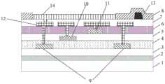
现有OLED显示基板的制作工艺中,如图1所示,是先形成显示基板的阳极14,再在形成有阳极14的基板上形成像素界定层8的图形,像素界定层8的图形具有多个能够暴露出阳极的开口,在制作完像素界定层8的图形后,还需要在像素界定层8的图形上制作PS(隔离柱)13,在制作PS13时需要在基板上涂覆有机感光材料,这些有机感光材料还会涂覆在阳极14上,由于阳极14位于像素界定层8的开口内,导致阳极14处于类似于孔洞的结构中,在经过制作隔离柱13的曝光显影工艺后,如图2所示,有机感光材料16容易残留在像素区域15的阳极上,将会影响显示基板的性能,降低OLED显示基板的良率。In the manufacturing process of the existing OLED display substrate, as shown in FIG. 1 , the
如果需要去除这些残留的有机感光材料,则还需要专门增加一道灰化工艺来去除残留在阳极上的有机感光材料,增加了OLED显示基板的制作工艺的复杂性,增加了OLED显示基板的制作成本。If these residual organic photosensitive materials need to be removed, a special ashing process needs to be added to remove the organic photosensitive materials remaining on the anode, which increases the complexity of the manufacturing process of the OLED display substrate and increases the manufacturing cost of the OLED display substrate .
为了解决上述问题,本发明的实施例提供一种OLED显示基板及其制作方法、显示装置,能够避免有机感光材料残留在阳极上,提高OLED显示基板的良率。In order to solve the above problems, embodiments of the present invention provide an OLED display substrate, a manufacturing method thereof, and a display device, which can prevent organic photosensitive materials from remaining on the anode and improve the yield of the OLED display substrate.
本发明实施例提供一种OLED显示基板的制作方法,包括在形成有阳极的基板上形成隔离柱的步骤和形成像素界定层的图形的步骤,所述形成隔离柱的步骤不迟于所述形成像素界定层的图形的步骤。An embodiment of the present invention provides a method for fabricating an OLED display substrate, which includes the steps of forming spacers on a substrate on which anodes are formed and a step of forming a pattern of a pixel definition layer, the step of forming spacers is not later than the step of forming Pixel defines the step of the layer's pattern.
本实施例中,形成隔离柱的步骤不迟于形成像素界定层的图形的步骤,可以在形成像素界定层的图形的步骤之前,形成隔离柱;或者通过一次构图工艺形成隔离柱和像素界定层的图形,这样在制作完像素界定层的图形后不用再在基板上涂覆有机感光材料,可以避免有机感光材料残留在阳极上,从而提高了OLED显示基板的良率。In this embodiment, the step of forming the isolation column is not later than the step of forming the pattern of the pixel definition layer, and the isolation column may be formed before the step of forming the pattern of the pixel definition layer; or the isolation column and the pixel definition layer may be formed by one patterning process In this way, the organic photosensitive material does not need to be coated on the substrate after the pattern of the pixel defining layer is formed, which can prevent the organic photosensitive material from remaining on the anode, thereby improving the yield of the OLED display substrate.
一具体实施例中,可以在所述形成像素界定层的图形的步骤之前,形成所述隔离柱。In a specific embodiment, the isolation pillars may be formed before the step of forming the pattern of the pixel definition layer.
进一步地,所述制作方法具体包括:Further, the manufacturing method specifically includes:
在形成有阳极的基板上涂覆一层有机感光材料;Coating a layer of organic photosensitive material on the substrate formed with the anode;
对所述有机感光材料进行曝光显影后形成所述隔离柱;forming the isolation column after exposing and developing the organic photosensitive material;
在形成有所述隔离柱的基板上涂覆一层绝缘材料,对所述绝缘材料进行构图形成所述像素界定层的图形。A layer of insulating material is coated on the substrate on which the isolation pillars are formed, and the insulating material is patterned to form a pattern of the pixel defining layer.
另一具体实施例中,可以通过一次构图工艺形成所述隔离柱和所述像素界定层的图形。In another specific embodiment, the patterns of the isolation pillars and the pixel defining layer may be formed through a single patterning process.
进一步地,所述制作方法具体包括:Further, the manufacturing method specifically includes:
在形成有阳极的基板上涂覆一层绝缘层;Coating an insulating layer on the substrate formed with the anode;
在所述绝缘层上涂覆一层光刻胶,曝光显影后形成光刻胶完全保留区域、光刻胶部分保留区域和光刻胶完全去除区域;A layer of photoresist is coated on the insulating layer, and after exposure and development, a photoresist complete retention area, a photoresist partial retention area and a photoresist complete removal area are formed;
刻蚀掉光刻胶完全去除区域的绝缘层;Etch away the insulating layer in the area where the photoresist is completely removed;
去除光刻胶部分保留区域的光刻胶,刻蚀掉光刻胶部分保留区域的部分厚度的绝缘层;Remove the photoresist in the partially reserved area of the photoresist, and etch away the insulating layer of the partial thickness in the partially reserved area of the photoresist;
去除光刻胶完全保留区域的光刻胶,形成绝缘层的图形,所述绝缘层的图形包括第一部分和凸设于所述第一部分上的第二部分,所述第一部分形成为所述像素界定层的图形,所述第二部分形成为所述隔离柱。removing the photoresist in the area where the photoresist is completely reserved to form a pattern of the insulating layer, the pattern of the insulating layer including a first part and a second part protruding on the first part, and the first part is formed as the pixel A pattern defining a layer, the second portion is formed as the isolation pillar.
进一步地,形成所述像素界定层的图形的步骤之后,所述制作方法还包括:Further, after the step of forming the pattern of the pixel definition layer, the manufacturing method further includes:
在形成有像素界定层的图形的基板上依次制备有机发光层和阴极。An organic light-emitting layer and a cathode are sequentially prepared on the substrate on which the pattern of the pixel defining layer is formed.
本发明实施例还提供了一种OLED显示基板,采用如上所述的制作方法制作得到。The embodiment of the present invention also provides an OLED display substrate, which is produced by the above-mentioned production method.
一具体实施例中,所述OLED显示基板具体包括:In a specific embodiment, the OLED display substrate specifically includes:
衬底基板;substrate substrate;
位于所述衬底基板上的薄膜晶体管阵列层;a thin film transistor array layer on the base substrate;
位于形成有所述薄膜晶体管阵列层的基板上的阳极;an anode on the substrate on which the thin film transistor array layer is formed;
位于形成有所述阳极的基板上的隔离柱;spacers on the substrate on which the anodes are formed;
位于形成有所述隔离柱的基板上、覆盖所述隔离柱的像素界定层的图形;a pattern of a pixel definition layer covering the isolation pillars on the substrate on which the isolation pillars are formed;
位于形成有所述像素界定层的图形的基板上的有机发光层和阴极。An organic light-emitting layer and a cathode on the substrate on which the pattern of the pixel defining layer is formed.
另一具体实施例中,所述OLED显示基板具体包括:In another specific embodiment, the OLED display substrate specifically includes:
衬底基板;substrate substrate;
位于所述衬底基板上的薄膜晶体管阵列层;a thin film transistor array layer on the base substrate;
位于形成有所述薄膜晶体管阵列层的基板上的阳极;an anode on the substrate on which the thin film transistor array layer is formed;
位于形成有所述阳极的基板上的绝缘层的图形,所述绝缘层的图形包括第一部分和凸设于所述第一部分上的第二部分,所述第一部分形成为所述像素界定层的图形,所述第二部分形成为所述隔离柱;A pattern of an insulating layer on the substrate on which the anode is formed, the pattern of the insulating layer including a first portion and a second portion protruding on the first portion, the first portion being formed as a part of the pixel defining layer a pattern, the second portion is formed as the isolation pillar;
位于形成有所述绝缘层的图形的基板上的有机发光层和阴极。An organic light-emitting layer and a cathode on the substrate on which the pattern of the insulating layer is formed.
下面结合具体实施例以及附图对本发明的OLED显示基板及其制作方法进行详细介绍:The OLED display substrate and its manufacturing method of the present invention will be described in detail below with reference to specific embodiments and accompanying drawings:
实施例一Example 1
本实施例中,是先形成隔离柱再形成像素界定层的图形。本实施例的OLED显示基板的制作方法包括:In this embodiment, the isolation column is formed first and then the pattern of the pixel defining layer is formed. The manufacturing method of the OLED display substrate of this embodiment includes:
步骤1、提供一硬质基板1,该硬质基板1可以为玻璃基板或石英基板;
步骤2、在硬质基板1上形成柔性基板2,柔性基板2可以采用聚酰亚胺制成;
步骤3、在柔性基板2上形成缓冲层3,缓冲层3可以采用氧化物、氮化物或者氧氮化合物制成;
步骤4、在缓冲层3上形成有源层9的图形;
具体地,在缓冲层3上沉积一层半导体材料,在半导体材料上涂覆一层光刻胶,采用掩膜板对光刻胶进行曝光,使光刻胶形成光刻胶未保留区域和光刻胶保留区域,其中,光刻胶保留区域对应于有源层9的图形所在区域,光刻胶未保留区域对应于有源层9的图形以外的区域;进行显影处理,光刻胶未保留区域的光刻胶被完全去除,通过刻蚀工艺完全刻蚀掉光刻胶未保留区域的半导体材料,形成有源层9的图形;去除掉光刻胶保留区域的光刻胶。Specifically, a layer of semiconductor material is deposited on the
步骤5、形成第一栅绝缘层4,第一栅绝缘层4可以选用氧化物、氮化物或者氧氮化合物,对应的反应气体是SiH4、NH3、N2或SiH2Cl2、NH3、N2;
步骤6、在第一栅绝缘层4上形成第一栅极10的图形;
具体地,可以采用溅射或热蒸发的方法在第一栅绝缘层4上沉积厚度约为
步骤7、形成第二栅绝缘层5,第二栅绝缘层5可以选用氧化物、氮化物或者氧氮化合物,对应的反应气体是SiH4、NH3、N2或SiH2Cl2、NH3、N2;Step 7, forming a second
步骤8、在第二栅绝缘层5上形成第二栅极11的图形;
具体地,可以采用溅射或热蒸发的方法在第二栅绝缘层5上沉积厚度约为
步骤9、形成层间绝缘层6,层间绝缘层6可以选用氧化物、氮化物或者氧氮化合物,对应的反应气体是SiH4、NH3、N2或SiH2Cl2、NH3、N2;
步骤10、在层间绝缘层6上形成源漏金属层12的图形;
具体地,可以在层间绝缘层6上采用磁控溅射、热蒸发或其它成膜方法沉积一层厚度约为
步骤11、形成平坦层7的图形,平坦层7可以采用有机树脂制成;Step 11, forming the pattern of the flat layer 7, the flat layer 7 can be made of organic resin;
步骤12、形成阳极14的图形;
具体地,在平坦层7上通过溅射或热蒸发的方法沉积厚度约为

步骤13、形成隔离柱13的图形;
具体地,在经过步骤12的基板上涂覆一层有机感光材料,对有机感光材料进行曝光显影后形成有机感光材料保留区域和有机感光材料去除区域,其中,有机感光材料保留区域保留的有机感光材料形成为隔离柱13;Specifically, a layer of organic photosensitive material is coated on the substrate after
步骤14、形成像素界定层8的图形;
具体地,在经过步骤13的基板上涂覆一层绝缘材料,在绝缘材料上涂覆一层光刻胶,采用掩膜板对光刻胶进行曝光,使光刻胶形成光刻胶未保留区域和光刻胶保留区域,其中,光刻胶保留区域对应于像素界定层8的图形所在区域,光刻胶未保留区域对应于上述图形以外的区域;进行显影处理,光刻胶未保留区域的光刻胶被完全去除,光刻胶保留区域的光刻胶厚度保持不变;通过刻蚀工艺完全刻蚀掉光刻胶未保留区域的绝缘材料,剥离剩余的光刻胶,形成像素界定层8的图形。Specifically, a layer of insulating material is coated on the substrate that has undergone
经过上述步骤1-14即可制作得到如图3所示的OLED显示基板,之后可以在OLED显示基板上制备有机发光层和阴极。本实施例在形成像素界定层的图形的步骤之前形成隔离柱,这样在制作完像素界定层的图形后不用再在基板上涂覆有机感光材料,如图5所示,可以避免有机感光材料残留在像素区域15的阳极上,从而提高了OLED显示基板的良率。After the above steps 1-14, the OLED display substrate shown in FIG. 3 can be produced, and then the organic light-emitting layer and the cathode can be prepared on the OLED display substrate. In this embodiment, the isolation column is formed before the step of forming the pattern of the pixel definition layer, so that after the pattern of the pixel definition layer is formed, the organic photosensitive material does not need to be coated on the substrate, as shown in FIG. 5, the organic photosensitive material can be prevented from remaining on the anode of the
实施例二
本实施例中,是通过一次构图工艺形成隔离柱和像素界定层的图形。本实施例的OLED显示基板的制作方法包括:In this embodiment, the pattern of the isolation column and the pixel defining layer is formed by one patterning process. The manufacturing method of the OLED display substrate of this embodiment includes:
步骤1、提供一硬质基板1,该硬质基板1可以为玻璃基板或石英基板;
步骤2、在硬质基板1上形成柔性基板2,柔性基板2可以采用聚酰亚胺制成;
步骤3、在柔性基板2上形成缓冲层3,缓冲层3可以采用氧化物、氮化物或者氧氮化合物制成;
步骤4、在缓冲层3上形成有源层9的图形;
具体地,在缓冲层3上沉积一层半导体材料,在半导体材料上涂覆一层光刻胶,采用掩膜板对光刻胶进行曝光,使光刻胶形成光刻胶未保留区域和光刻胶保留区域,其中,光刻胶保留区域对应于有源层9的图形所在区域,光刻胶未保留区域对应于有源层9的图形以外的区域;进行显影处理,光刻胶未保留区域的光刻胶被完全去除,通过刻蚀工艺完全刻蚀掉光刻胶未保留区域的半导体材料,形成有源层9的图形;去除掉光刻胶保留区域的光刻胶。Specifically, a layer of semiconductor material is deposited on the
步骤5、形成第一栅绝缘层4,第一栅绝缘层4可以选用氧化物、氮化物或者氧氮化合物,对应的反应气体是SiH4、NH3、N2或SiH2Cl2、NH3、N2;
步骤6、在第一栅绝缘层4上形成第一栅极10的图形;
具体地,可以采用溅射或热蒸发的方法在第一栅绝缘层4上沉积厚度约为
步骤7、形成第二栅绝缘层5,第二栅绝缘层5可以选用氧化物、氮化物或者氧氮化合物,对应的反应气体是SiH4、NH3、N2或SiH2Cl2、NH3、N2;Step 7, forming a second
步骤8、在第二栅绝缘层5上形成第二栅极11的图形;
具体地,可以采用溅射或热蒸发的方法在第二栅绝缘层5上沉积厚度约为
步骤9、形成层间绝缘层6,层间绝缘层6可以选用氧化物、氮化物或者氧氮化合物,对应的反应气体是SiH4、NH3、N2或SiH2Cl2、NH3、N2;
步骤10、在层间绝缘层6上形成源漏金属层12的图形;
具体地,可以在层间绝缘层6上采用磁控溅射、热蒸发或其它成膜方法沉积一层厚度约为
步骤11、形成平坦层7的图形,平坦层7可以采用有机树脂制成;Step 11, forming the pattern of the flat layer 7, the flat layer 7 can be made of organic resin;
步骤12、形成阳极14的图形;
具体地,在平坦层7上通过溅射或热蒸发的方法沉积厚度约为

步骤13、形成隔离柱13和像素界定层8的图形;
具体地,在经过步骤12的基板上涂覆一层绝缘层;在绝缘层上涂覆一层光刻胶,曝光显影后形成光刻胶完全保留区域、光刻胶部分保留区域和光刻胶完全去除区域;刻蚀掉光刻胶完全去除区域的绝缘层;去除光刻胶部分保留区域的光刻胶,刻蚀掉光刻胶部分保留区域的部分厚度的绝缘层;去除光刻胶完全保留区域的光刻胶,形成绝缘层的图形,绝缘层的图形包括第一部分和凸设于第一部分上的第二部分,第一部分形成为像素界定层8的图形,第二部分形成为隔离柱13。Specifically, a layer of insulating layer is coated on the substrate after
经过上述步骤1-13即可制作得到如图4所示的OLED显示基板,之后可以在OLED显示基板上制备有机发光层和阴极。本实施例通过一次构图工艺形成像素界定层的图形和隔离柱,这样在制作完像素界定层的图形后不用再在基板上涂覆有机感光材料,如图5所示,可以避免有机感光材料残留在像素区域15的阳极上,从而提高了OLED显示基板的良率。After the above steps 1-13, the OLED display substrate shown in FIG. 4 can be produced, and then the organic light-emitting layer and the cathode can be prepared on the OLED display substrate. In this embodiment, the pattern of the pixel definition layer and the isolation column are formed by one patterning process, so that after the pattern of the pixel definition layer is finished, the organic photosensitive material does not need to be coated on the substrate, as shown in FIG. 5 , the residue of the organic photosensitive material can be avoided. on the anode of the
本发明实施例还提供了一种显示装置,包括如上所述的OLED显示基板。所述显示装置可以为:电视、显示器、数码相框、手机、平板电脑等任何具有显示功能的产品或部件,其中,所述显示装置还包括柔性电路板、印刷电路板和背板。Embodiments of the present invention also provide a display device including the OLED display substrate as described above. The display device can be any product or component with a display function, such as a TV, a monitor, a digital photo frame, a mobile phone, a tablet computer, etc., wherein the display device further includes a flexible circuit board, a printed circuit board and a backplane.
在本发明各方法实施例中,所述各步骤的序号并不能用于限定各步骤的先后顺序,对于本领域普通技术人员来讲,在不付出创造性劳动的前提下,对各步骤的先后变化也在本发明的保护范围之内。In the method embodiments of the present invention, the sequence numbers of the steps cannot be used to define the sequence of the steps. For those of ordinary skill in the art, the sequence of the steps can be changed without creative work. It also falls within the protection scope of the present invention.
除非另外定义,本公开使用的技术术语或者科学术语应当为本发明所属领域内具有一般技能的人士所理解的通常意义。本公开中使用的“第一”、“第二”以及类似的词语并不表示任何顺序、数量或者重要性,而只是用来区分不同的组成部分。“包括”或者“包含”等类似的词语意指出现该词前面的元件或者物件涵盖出现在该词后面列举的元件或者物件及其等同,而不排除其他元件或者物件。“连接”或者“相连”等类似的词语并非限定于物理的或者机械的连接,而是可以包括电性的连接,不管是直接的还是间接的。“上”、“下”、“左”、“右”等仅用于表示相对位置关系,当被描述对象的绝对位置改变后,则该相对位置关系也可能相应地改变。Unless otherwise defined, technical or scientific terms used in this disclosure should have the ordinary meaning as understood by one of ordinary skill in the art to which this invention belongs. As used in this disclosure, "first," "second," and similar terms do not denote any order, quantity, or importance, but are merely used to distinguish the various components. "Comprises" or "comprising" and similar words mean that the elements or things appearing before the word encompass the elements or things recited after the word and their equivalents, but do not exclude other elements or things. Words like "connected" or "connected" are not limited to physical or mechanical connections, but may include electrical connections, whether direct or indirect. "Up", "Down", "Left", "Right", etc. are only used to represent the relative positional relationship, and when the absolute position of the described object changes, the relative positional relationship may also change accordingly.
可以理解,当诸如层、膜、区域或基板之类的元件被称作位于另一元件“上”或“下”时,该元件可以“直接”位于另一元件“上”或“下”,或者可以存在中间元件。It will be understood that when an element such as a layer, film, region or substrate is referred to as being "on" or "under" another element, it can be "directly on" or "under" the other element, Or intermediate elements may be present.
以上所述是本发明的优选实施方式,应当指出,对于本技术领域的普通技术人员来说,在不脱离本发明所述原理的前提下,还可以作出若干改进和润饰,这些改进和润饰也应视为本发明的保护范围。The above are the preferred embodiments of the present invention. It should be pointed out that for those skilled in the art, without departing from the principles of the present invention, several improvements and modifications can be made. It should be regarded as the protection scope of the present invention.
Claims (5)
Translated fromChinesePriority Applications (2)
| Application Number | Priority Date | Filing Date | Title |
|---|---|---|---|
| CN201710631205.3ACN107302061B (en) | 2017-07-28 | 2017-07-28 | OLED display substrate, manufacturing method thereof and display device |
| US15/970,863US10504975B2 (en) | 2017-07-28 | 2018-05-03 | Organic light-emitting diode display substrate, manufacturing method thereof and display device |
Applications Claiming Priority (1)
| Application Number | Priority Date | Filing Date | Title |
|---|---|---|---|
| CN201710631205.3ACN107302061B (en) | 2017-07-28 | 2017-07-28 | OLED display substrate, manufacturing method thereof and display device |
Publications (2)
| Publication Number | Publication Date |
|---|---|
| CN107302061A CN107302061A (en) | 2017-10-27 |
| CN107302061Btrue CN107302061B (en) | 2020-06-30 |
Family
ID=60133222
Family Applications (1)
| Application Number | Title | Priority Date | Filing Date |
|---|---|---|---|
| CN201710631205.3AActiveCN107302061B (en) | 2017-07-28 | 2017-07-28 | OLED display substrate, manufacturing method thereof and display device |
Country Status (2)
| Country | Link |
|---|---|
| US (1) | US10504975B2 (en) |
| CN (1) | CN107302061B (en) |
Families Citing this family (6)
| Publication number | Priority date | Publication date | Assignee | Title |
|---|---|---|---|---|
| CN107180925B (en)* | 2017-07-20 | 2019-07-16 | 京东方科技集团股份有限公司 | Fabrication method of array substrate and fabrication method of display device |
| JP7485484B2 (en)* | 2019-12-11 | 2024-05-16 | 京東方科技集團股▲ふん▼有限公司 | Display substrate, its manufacturing method, and display device |
| KR20210102558A (en)* | 2020-02-11 | 2021-08-20 | 삼성디스플레이 주식회사 | Display apparatus |
| CN111276524B (en)* | 2020-02-13 | 2022-07-22 | 京东方科技集团股份有限公司 | Method for manufacturing an array substrate, array substrate and display panel |
| CN113451359B (en)* | 2020-03-24 | 2022-10-21 | 昆山国显光电有限公司 | Display panel, manufacturing method thereof and display device |
| CN115513264A (en)* | 2022-09-22 | 2022-12-23 | 京东方科技集团股份有限公司 | Display substrate, manufacturing method thereof and display device |
Citations (3)
| Publication number | Priority date | Publication date | Assignee | Title |
|---|---|---|---|---|
| CN101800293A (en)* | 2010-03-15 | 2010-08-11 | 彩虹集团公司 | Manufacturing method of organic light emitting diode, insulation layer and isolation column thereof |
| CN103489827A (en)* | 2013-09-27 | 2014-01-01 | 京东方科技集团股份有限公司 | Thin film transistor driving backplane, manufacturing method thereof and display panel |
| CN104538558A (en)* | 2014-12-25 | 2015-04-22 | 昆山国显光电有限公司 | OLED device and method thereof |
Family Cites Families (3)
| Publication number | Priority date | Publication date | Assignee | Title |
|---|---|---|---|---|
| KR100840117B1 (en)* | 2007-09-05 | 2008-06-19 | 삼성에스디아이 주식회사 | Light emitting display device and manufacturing method thereof |
| US9508778B2 (en)* | 2014-04-25 | 2016-11-29 | Samsung Display Co., Ltd. | Organic light emitting diode display |
| CN104810382A (en)* | 2015-05-07 | 2015-07-29 | 深圳市华星光电技术有限公司 | AMOLED (active matrix/organic light emitting diode) backboard production method and AMOLED backboard structure |
- 2017
- 2017-07-28CNCN201710631205.3Apatent/CN107302061B/enactiveActive
- 2018
- 2018-05-03USUS15/970,863patent/US10504975B2/enactiveActive
Patent Citations (3)
| Publication number | Priority date | Publication date | Assignee | Title |
|---|---|---|---|---|
| CN101800293A (en)* | 2010-03-15 | 2010-08-11 | 彩虹集团公司 | Manufacturing method of organic light emitting diode, insulation layer and isolation column thereof |
| CN103489827A (en)* | 2013-09-27 | 2014-01-01 | 京东方科技集团股份有限公司 | Thin film transistor driving backplane, manufacturing method thereof and display panel |
| CN104538558A (en)* | 2014-12-25 | 2015-04-22 | 昆山国显光电有限公司 | OLED device and method thereof |
Also Published As
| Publication number | Publication date |
|---|---|
| CN107302061A (en) | 2017-10-27 |
| US10504975B2 (en) | 2019-12-10 |
| US20190035864A1 (en) | 2019-01-31 |
Similar Documents
| Publication | Publication Date | Title |
|---|---|---|
| CN107302061B (en) | OLED display substrate, manufacturing method thereof and display device | |
| CN111524957B (en) | Display substrate, manufacturing method thereof and display device | |
| CN109360843B (en) | OLED display substrate, manufacturing method thereof and display device | |
| US11348987B2 (en) | OLED display substrate having large aperture ratio, method of manufacturing the same, and display device | |
| CN110400810B (en) | Display substrate, manufacturing method thereof and display device | |
| WO2015100898A1 (en) | Thin-film transistor, tft array substrate and manufacturing method therefor, and display device | |
| CN104795434A (en) | OLED pixel unit, transparent display device, manufacturing method and display equipment | |
| CN111430428B (en) | Flexible display panel, manufacturing method thereof and display device | |
| CN108400151B (en) | Display substrate, manufacturing method thereof, and display device | |
| CN103474453B (en) | El light emitting device and preparation method thereof | |
| CN111627972B (en) | A display substrate, its manufacturing method, a display panel, and a display device | |
| CN104465510A (en) | Array substrate, manufacturing method of array substrate and display panel | |
| CN101740726B (en) | Organic electroluminescent device and manufacturing method thereof | |
| CN108538782A (en) | Oled display substrate and preparation method thereof, display device | |
| CN111244326A (en) | OLED display substrate, manufacturing method thereof and display device | |
| CN109036134A (en) | Flexible display substrates and preparation method thereof, display device | |
| CN103489874B (en) | Array base palte and preparation method thereof, display unit | |
| CN107369777B (en) | OLED substrate, preparation method thereof and display device | |
| CN111584758B (en) | Display substrate, manufacturing method thereof, and display device | |
| CN103500746A (en) | Array substrate, manufacturing method of array substrate and display device | |
| WO2021238481A1 (en) | Oled display substrate and manufacturing method therefor, and display apparatus | |
| CN106449519B (en) | A kind of thin film transistor (TFT) and production method, display device | |
| CN113782581B (en) | Display panel, manufacturing method thereof, and display device | |
| CN110890481B (en) | Display substrate, preparation method thereof and display device | |
| CN107146855A (en) | OLED substrate, manufacturing method thereof, and display device |
Legal Events
| Date | Code | Title | Description |
|---|---|---|---|
| PB01 | Publication | ||
| PB01 | Publication | ||
| SE01 | Entry into force of request for substantive examination | ||
| SE01 | Entry into force of request for substantive examination | ||
| GR01 | Patent grant | ||
| GR01 | Patent grant |