CN107291425B - System and method for incorporating partially written results that resolve renaming size issues - Google Patents
System and method for incorporating partially written results that resolve renaming size issuesDownload PDFInfo
- Publication number
- CN107291425B CN107291425BCN201710491888.7ACN201710491888ACN107291425BCN 107291425 BCN107291425 BCN 107291425BCN 201710491888 ACN201710491888 ACN 201710491888ACN 107291425 BCN107291425 BCN 107291425B
- Authority
- CN
- China
- Prior art keywords
- instruction
- merge
- instructions
- architectural
- merged
- Prior art date
- Legal status (The legal status is an assumption and is not a legal conclusion. Google has not performed a legal analysis and makes no representation as to the accuracy of the status listed.)
- Active
Links
Images


Classifications
- G—PHYSICS
- G06—COMPUTING OR CALCULATING; COUNTING
- G06F—ELECTRIC DIGITAL DATA PROCESSING
- G06F9/00—Arrangements for program control, e.g. control units
- G06F9/06—Arrangements for program control, e.g. control units using stored programs, i.e. using an internal store of processing equipment to receive or retain programs
- G06F9/30—Arrangements for executing machine instructions, e.g. instruction decode
- G06F9/38—Concurrent instruction execution, e.g. pipeline or look ahead
- G06F9/3836—Instruction issuing, e.g. dynamic instruction scheduling or out of order instruction execution
- G06F9/3838—Dependency mechanisms, e.g. register scoreboarding
- G06F9/384—Register renaming
- G—PHYSICS
- G06—COMPUTING OR CALCULATING; COUNTING
- G06F—ELECTRIC DIGITAL DATA PROCESSING
- G06F9/00—Arrangements for program control, e.g. control units
- G06F9/06—Arrangements for program control, e.g. control units using stored programs, i.e. using an internal store of processing equipment to receive or retain programs
- G06F9/30—Arrangements for executing machine instructions, e.g. instruction decode
- G06F9/30098—Register arrangements
- G06F9/30105—Register structure
- G06F9/30112—Register structure comprising data of variable length
- G—PHYSICS
- G06—COMPUTING OR CALCULATING; COUNTING
- G06F—ELECTRIC DIGITAL DATA PROCESSING
- G06F9/00—Arrangements for program control, e.g. control units
- G06F9/06—Arrangements for program control, e.g. control units using stored programs, i.e. using an internal store of processing equipment to receive or retain programs
- G06F9/30—Arrangements for executing machine instructions, e.g. instruction decode
- G06F9/30098—Register arrangements
- G06F9/3012—Organisation of register space, e.g. banked or distributed register file
- G06F9/30123—Organisation of register space, e.g. banked or distributed register file according to context, e.g. thread buffers
- G—PHYSICS
- G06—COMPUTING OR CALCULATING; COUNTING
- G06F—ELECTRIC DIGITAL DATA PROCESSING
- G06F9/00—Arrangements for program control, e.g. control units
- G06F9/06—Arrangements for program control, e.g. control units using stored programs, i.e. using an internal store of processing equipment to receive or retain programs
- G06F9/30—Arrangements for executing machine instructions, e.g. instruction decode
- G06F9/3017—Runtime instruction translation, e.g. macros
- G—PHYSICS
- G06—COMPUTING OR CALCULATING; COUNTING
- G06F—ELECTRIC DIGITAL DATA PROCESSING
- G06F9/00—Arrangements for program control, e.g. control units
- G06F9/06—Arrangements for program control, e.g. control units using stored programs, i.e. using an internal store of processing equipment to receive or retain programs
- G06F9/30—Arrangements for executing machine instructions, e.g. instruction decode
- G06F9/30181—Instruction operation extension or modification
- G—PHYSICS
- G06—COMPUTING OR CALCULATING; COUNTING
- G06F—ELECTRIC DIGITAL DATA PROCESSING
- G06F9/00—Arrangements for program control, e.g. control units
- G06F9/06—Arrangements for program control, e.g. control units using stored programs, i.e. using an internal store of processing equipment to receive or retain programs
- G06F9/30—Arrangements for executing machine instructions, e.g. instruction decode
- G06F9/38—Concurrent instruction execution, e.g. pipeline or look ahead
- G06F9/3836—Instruction issuing, e.g. dynamic instruction scheduling or out of order instruction execution
- G—PHYSICS
- G06—COMPUTING OR CALCULATING; COUNTING
- G06F—ELECTRIC DIGITAL DATA PROCESSING
- G06F9/00—Arrangements for program control, e.g. control units
- G06F9/06—Arrangements for program control, e.g. control units using stored programs, i.e. using an internal store of processing equipment to receive or retain programs
- G06F9/30—Arrangements for executing machine instructions, e.g. instruction decode
- G06F9/38—Concurrent instruction execution, e.g. pipeline or look ahead
- G06F9/3854—Instruction completion, e.g. retiring, committing or graduating
- G06F9/3856—Reordering of instructions, e.g. using queues or age tags
Landscapes
- Engineering & Computer Science (AREA)
- Software Systems (AREA)
- Theoretical Computer Science (AREA)
- Physics & Mathematics (AREA)
- General Engineering & Computer Science (AREA)
- General Physics & Mathematics (AREA)
- Advance Control (AREA)
Abstract
Translated fromChinese
Description
Translated fromChinese技术领域technical field
本发明一般涉及寄存器重命名以解决处理器中存储的结果尺寸问题,更具体地涉及一种插入合并指令以合并部分写入结果的系统和方法。The present invention relates generally to register renaming to address results size issues stored in processors, and more particularly to a system and method for inserting a coalescing instruction to coalesce partially written results.
背景技术Background technique
处理器包括一组寄存器以存储写入操作的结果。写操作由处理器的标准指令集架构(ISA)的子集执行,例如英特尔
在执行软件程序或应用程序期间,当遇到引用架构寄存器以存储指令结果的指令时,处理器从物理寄存器索引的“空闲列表(freelist)”中分配可用的物理寄存器,附加或否则分配所选索引给指令,并更新重命名结构的推测部分以将架构寄存器映射到所选择的物理寄存器。当指令执行时,索引用于访问物理寄存器以存储结果。当指令退出时,索引可以被移动到重命名结构的退出部分(或者被移动到不同的重命名结构),以将物理寄存器映射到特定的架构寄存器。物理到架构寄存器映射可以由随后的读取操作使用,直到被重写或重新定义。不需要单独的一组物理架构寄存器;而是将架构标识符等简单地映射到物理寄存器索引。PRF重命名风格更有效,因为索引只是简单地移动或重新映射,而不必在寄存器之间移动值。During execution of a software program or application, when an instruction is encountered that refers to an architectural register to store the result of the instruction, the processor allocates available physical registers from a "freelist" indexed by physical registers, appends or otherwise allocates the selected physical registers The index is given to the instruction, and the speculative portion of the rename structure is updated to map the architectural registers to the chosen physical registers. When the instruction executes, the index is used to access the physical register to store the result. When an instruction exits, the index can be moved to the exit portion of the rename structure (or moved to a different rename structure) to map physical registers to specific architectural registers. The physical-to-architectural register map can be used by subsequent read operations until overwritten or redefined. There is no need for a separate set of physical architectural registers; instead, architectural identifiers etc. are simply mapped to physical register indices. The PRF renaming style is more efficient, because the index is simply moved or remapped without having to move the value between registers.
当架构使用允许部分写入操作仅修改整个寄存器的一部分的复杂操作数尺寸时,出现尺寸问题。例如,X86架构使用这种复杂的操作数尺寸,尽管本发明不限于X86架构。作为复杂操作数尺寸的示例,可以执行写入指令来修改64位寄存器的8位、16位、32位或64位,其中每个较大的尺寸包含较小的写入尺寸(因为被引用到寄存器的公共端)。即使引用同一架构寄存器,每个指令也可以被分配一个单独的物理寄存器。与同一架构寄存器的先前写操作相同尺寸或比其尺寸大的后续写操作在系统中得到适当处理,无需进一步修改。然而,对相同的架构寄存器的后续写入操作小于之前的写入操作会造成随后的引用该相同的架构寄存器的较大读取操作的问题,因为没有单个物理寄存器保存该架构寄存器的完整结果。Size issues arise when architectures use complex operand sizes that allow partial write operations to modify only a portion of the entire register. For example, the X86 architecture uses this complex operand size, although the invention is not limited to the X86 architecture. As an example of a complex operand size, a write instruction can be executed to modify 8-bit, 16-bit, 32-bit, or 64-bit of a 64-bit register, where each larger size contains a smaller write size (as referenced to register common). Each instruction can be allocated a separate physical register even if it refers to the same architectural register. Subsequent writes of the same size or larger than previous writes to the same architectural register are handled appropriately in the system without further modification. However, subsequent writes to the same architectural register that are smaller than previous write operations can cause problems for subsequent larger reads referencing the same architectural register, since no single physical register holds the complete result of that architectural register.
发明内容SUMMARY OF THE INVENTION
根据一个实施例的处理器包括具有多个物理寄存器的物理寄存器文件、映射逻辑和合并系统。对于接收到的程序指令中特定的每个架构寄存器,映射逻辑映射最多第一最大数量的物理寄存器,并将对应的映射存储在重命名表中。合并系统为需要合并的每个架构寄存器生成合并指令,将每个合并指令插入到程序指令中,以提供经过修改的指令组,并根据采取规则在连续的发布周期中发布修改后的指令组。在一个实施例中,第一最大数量可以是二。A processor according to one embodiment includes a physical register file having a plurality of physical registers, mapping logic, and a merge system. For each architectural register specified in the received program instruction, the mapping logic maps up to the first maximum number of physical registers and stores the corresponding mappings in the renaming table. The merge system generates merge instructions for each architectural register that needs to be merged, inserts each merge instruction into a program instruction to provide a modified instruction group, and issues the modified instruction group in successive issue cycles according to take rules. In one embodiment, the first maximum number may be two.
合并系统可以包括合并检测器、合并指令生成器、合并采取逻辑和指令发布逻辑。合并检测器检测读取指令是否读取映射到多个物理寄存器的架构寄存器的,检测写指令是否会导致映射超过所述第一最大数,并且生成标识任何架构寄存器的合并的合并标识符。合并指令生成器根据合并标识符生成要合并的每个架构寄存器的合并指令。合并采取逻辑基于所述采取规则确定哪一个合并指令应该在所述多个程序指令中的任何一个之前被插入,并产生指示每个时钟周期发布哪些指令的终止指示。指令发布逻辑提供基于终止指示的发布指令控制。The merge system may include a merge detector, a merge instruction generator, merge take logic, and instruction issue logic. A coalescing detector detects whether a read instruction reads architectural registers mapped to multiple physical registers, detects whether a write instruction would cause a map to exceed the first maximum number, and generates a coalescing identifier identifying any architectural register coalescing. The merge instruction generator generates a merge instruction for each architectural register to be merged based on the merge identifier. The merge take logic determines which merge instruction should be inserted before any of the plurality of program instructions based on the take rules, and generates a termination indication indicating which instructions to issue each clock cycle. The instruction issue logic provides issue instruction control based on termination indications.
指令发布逻辑可以包括指令重排序模块,其接收终止指示、程序指令以及由合并指令生成器产生的任何合并指令,并且提供发布指令控制以控制在每个时钟周期内发布的指令。The instruction issue logic may include an instruction reordering module that receives termination indications, program instructions, and any merged instructions generated by the merged instruction generator, and provides issue instruction control to control which instructions are issued in each clock cycle.
指令发布逻辑可以包括指令移位器和指令重排序模块。指令移位器根据终止指令移动程序指令。指令重排序模块接收程序指令和由合并指令生成器生成的任何合并指令,并提供发布指令控制以控制在每个时钟周期内发布的指令。The instruction issue logic may include an instruction shifter and an instruction reordering module. The instruction shifter moves program instructions according to the termination instruction. The instruction reordering module receives program instructions and any merged instructions generated by the merged instruction generator, and provides issue instruction control to control which instructions are issued in each clock cycle.
根据一个实施例,合并用于解决处理器的重命名尺寸问题的部分写入结果的方法包括:将重命名表中的多个程序指令中特定的多个架构寄存器中的每一个映射到最多第一最大数量的多个物理寄存器,在执行至少一个程序指令之前,检测任何架构寄存器何时需要被合并,为需要合并的每个架构寄存器生成合并指令,将每个合并指令插入到程序指令中以提供修改的指令组,并且基于建立相应的定时和性能折衷的采取规则在连续的时钟周期内发布经修改的指令组。第一最大数量可能是二。According to one embodiment, a method of consolidating partial write results for addressing a rename size problem of a processor includes mapping each of a particular plurality of architectural registers of a plurality of program instructions in a rename table to at most the first a maximum number of multiple physical registers, before executing at least one program instruction, detect when any architectural registers need to be merged, generate a merge instruction for each architectural register that needs to be merged, insert each merge instruction into the program instruction to A modified set of instructions is provided and issued in successive clock cycles based on adoption rules that establish corresponding timing and performance tradeoffs. The first maximum number possible is two.
该方法可以包括检测读取指令是否读取映射到多个物理寄存器的架构寄存器,以及生成相应的读取合并指令。该方法可以包括检测写入指令是否使得映射的超过第一最大数量,并且生成相应的写入合并指令。The method may include detecting whether a read instruction reads an architectural register mapped to a plurality of physical registers, and generating a corresponding read merge instruction. The method may include detecting whether a write instruction causes the mapping to exceed a first maximum number, and generating a corresponding write coalescing instruction.
该方法可以包括基于检测来生成标识需要被合并的任何架构寄存器的合并标识符,并且在生成和发布期间使用合并标识符。The method may include generating, based on the detection, a merge identifier that identifies any architectural registers that need to be merged, and using the merge identifier during generation and publishing.
该方法可以包括基于采取规则确定任何生成的合并指令中的哪一个应当在任何程序指令之前被插入,产生指示每个时钟周期发布哪些指令的终止指示,以及基于终止指示提供发布指令控制。The method may include determining which of any generated merged instructions should be inserted before any program instructions based on a take rule, generating a termination indication indicating which instructions to issue each clock cycle, and providing issue instruction control based on the termination indication.
该方法可以包括从多个采用规则中选择一个采用规则,其中每个采用规则在时序和性能之间提供不同的折衷。The method may include selecting an adoption rule from a plurality of adoption rules, wherein each adoption rule provides a different tradeoff between timing and performance.
附图说明Description of drawings
关于以下描述和附图,将更好地理解本发明的益处、特征和优点,其中:The benefits, features and advantages of the present invention will be better understood with respect to the following description and accompanying drawings, wherein:
图1是根据本发明的一个实施例所述的超标量流水线处理器的框图;1 is a block diagram of a superscalar pipelined processor according to an embodiment of the present invention;
图2是在执行指令μop1和μop2之后并且在执行μop3之前根据本发明的一个实施例的图1的重命名表的至少一部分的图;FIG. 2 is a diagram of at least a portion of the rename table of FIG. 1 after execution of instructions μop1 and μop2 and before execution of μop3, according to one embodiment of the present invention;
图3是在执行指令μop1,μop2,μopM和μop 3之后,根据本发明的一个实施例的图1的重命名表的至少一部分的图;3 is a diagram of at least a portion of the renaming table of FIG. 1 after execution of instructions μop1, μop2, μopM, and μop3, according to one embodiment of the present invention;
图4是根据本发明的一个实施例的图1的重命名表的至少一部分的图;FIG. 4 is a diagram of at least a portion of the rename table of FIG. 1 according to one embodiment of the present invention;
图5是示出根据本发明的一个实施例实现图1的合并系统的框图;5 is a block diagram illustrating the implementation of the merging system of FIG. 1 according to one embodiment of the present invention;
图6是示出根据本发明的另一个实施例实现的图1的合并系统的框图1;以及FIG. 6 is a block diagram 1 illustrating the merging system of FIG. 1 implemented in accordance with another embodiment of the present invention; and
图7是示出根据本发明的实施例的示例性采取规则的示意图。FIG. 7 is a schematic diagram illustrating an exemplary adoption rule according to an embodiment of the present invention.
具体实施方式Detailed ways
本发明人已经认识到由使用复杂操作数尺寸的指令集架构引起的PRF重命名风格的尺寸问题。因此,他们开发了一种插入合并指令以合并部分写入结果以将部分写入结果保持在预定最大值并允许后续读取操作的系统和方法。The inventors have recognized the size issues of the PRF renaming style caused by instruction set architectures that use complex operand sizes. Therefore, they developed a system and method for inserting a merge instruction to merge partial write results to keep the partial write results at a predetermined maximum value and allow subsequent read operations.
图1是根据本发明的一个实施例实现的超标量流水线处理器100的简化框图。本文所用的术语“处理器”是指包括微处理器、中央处理单元(CPU)、处理核心、微控制器等的任何类型的处理单元。本文所用的术语“处理器”还包括任何类型的处理器配置,例如集成在芯片或集成电路(IC)上的一个或多个处理单元,包括集成在芯片上系统(SOC)等中的处理器配置。处理器100包括高速缓存诸如X86指令集架构等的指令集架构(ISA)的宏指令的指令高速缓存102。考虑了允许复杂操作数尺寸的额外的或替代的指令集架构。处理器100包括指令转换器104,其接收宏指令并将宏指令转换成微指令。微指令通常可以被称为微指令,但是在本文中更一般地简称为“指令”,或者甚至更简单地称为“μops”。然后将微指令以程序顺序提供给寄存器别名表(RAT)106,寄存器别名表106产生微指令依赖性并将程序顺序的微指令发布到保留站(RS)108和重排序缓冲器(ROB,reorder buffer)110。ROB 110存储从RAT 106发布的每条指令的条目,并确保已发布的指令按顺序退出。1 is a simplified block diagram of a superscalar pipelined
保留站RS 108将指令调度到多个执行单元112中的适当的一个,保留站RS 108也可称为分派器。在一个实施例中,处理器100是无序(OOO,out of order)处理器,其中当保留站108准备不是严格按照程序顺序执行指令时,可以将指令分派给执行单元112。当其所有依赖性被解决并且适当的执行单元112可用于执行指令时,指令被视为准备执行。寄存器别名表106确定并将相关性信息转发给保留站108用于所发布的指令,并且RS 108使用依赖性信息来确定何时分派用于执行的指令。虽然没有具体示出,但是执行单元112可以包括一个或多个整数执行单元(例如整数算术/逻辑单元(ALU)等)、一个或多个浮点执行单元(诸如包括单指令多数据(SIMD)执行单元,例如MMX和SSE单元等)、存储器顺序缓冲器(MOB)等。写入指令的任何结果通过回写(WB)路径被写入一个物理寄存器文件(PRF)114内的物理寄存器。与写指令对应的ROB 110的条目将索引存储到用于写入结果的物理寄存器。The
RAT 106包括重命名表116、映射逻辑118、空闲列表120和合并系统122。重命名表116将架构寄存器交叉引用或映射到PRF 114的物理寄存器。空闲列表120将索引列表存储到未分配的相应物理寄存器。当写入操作引用用于存储结果的架构寄存器时,映射逻辑118参考重命名表116来确定架构寄存器是否已被映射。如果还没有映射,则映射逻辑118参考空闲列表120并选择和分配物理寄存器。然后,映射逻辑118将分配的物理寄存器的索引存储到与写入指令中引用的架构寄存器对应的重命名表116的条目中。以这种方式,物理寄存器最初映射到架构寄存器和写指令。如本文进一步描述的,响应于一个或多个部分写指令,每个架构寄存器可被映射到多个物理寄存器,其中架构寄存器的完整内容分布在多个物理寄存器中,因此不存储在某一个物理寄存器。重命名表116可以被配置为映射到达预定数量的“N”个物理寄存器,其中执行合并操作以将总映射数保持在N或N以下,如本文进一步描述的。
合并系统122分析从指令转换器104提供的μops的源和/或目的地,以确定存储在映射到所指示的架构寄存器的多个物理寄存器中的部分结果是否需要被合并到单个物理寄存器。对于需要合并的每个架构寄存器,合并系统122生成合并指令并将合并指令插入到指令流中。合并系统122确定每个合并指令将要被插入的位置,并根据这里进一步描述的适用的采取规则进一步确定每个周期中要向RS 108发布的μops。如由合并系统122建立的排序和编号所指示的,如本文进一步描述的,RAT 106然后向RS 108发布μops。
用于处理器100的ISA(例如所示配置中的X86)使用复杂的操作数尺寸,允许对每个架构寄存器进行部分写入。X86架构包括可以使用多种尺寸访问的多个架构寄存器。64位版本包括寄存器符号RAX、RBX、RCX、RDX等(64位使用预先提供的'R'符号),其中使用任何这些64位符号的写操作是写入整个寄存器。这些寄存器分别包括32位符号EAX、EBX、ECX、EDX等(32位使用预先提供的'E'符号)以及16位符号AX、BX、CX、DX等(16位仅使用寄存器名称而没有预先提供的字母)。也可以定义8位符号,但是每个符号通常都是16位版本的最高有效字节(MSB)或最低有效字节(LSB),不再进一步描述。重命名表116中的架构标识符仅需要包括用于任何给定寄存器或其部分的单个引用。The ISA for processor 100 (eg, X86 in the configuration shown) uses a complex operand size, allowing partial writes to each architectural register. The x86 architecture includes several architectural registers that can be accessed using various sizes. The 64-bit version includes the register symbols RAX, RBX, RCX, RDX, etc. (64-bit uses the pre-supplied 'R' symbol), where a write using any of these 64-bit symbols is writing the entire register. These registers include the 32-bit symbols EAX, EBX, ECX, EDX, etc. respectively (32-bit uses the pre-supplied 'E' notation) and the 16-bit symbols AX, BX, CX, DX, etc. (16-bit only uses the register name without pre-supplied letters). 8-bit symbols can also be defined, but each symbol is usually the most significant byte (MSB) or least significant byte (LSB) of the 16-bit version and is not described further. The architectural identifiers in the rename table 116 need only include a single reference for any given register or portion thereof.
当一系列μop指令使用复杂操作数尺寸时,其中多个物理寄存器存储相同架构寄存器的部分,当尝试读取架构寄存器时,挑战出现。例如,考虑以下指令模式:Challenges arise when attempting to read architectural registers when a series of μop instructions use complex operand sizes, where multiple physical registers store portions of the same architectural register. For example, consider the following instruction pattern:
μop 1)MOV RAX,RBXμop 1) MOV RAX, RBX
μop 2)MOV EAX,ECXμop 2) MOV EAX, ECX
μop 3)MOV RSP,RAXμop 3) MOV RSP, RAX
为第一MOV指令(μop 1)分配第一物理寄存器,并将分配的物理寄存器映射到RAX架构寄存器。第一MOV指令μop 1指示处理器100将64位寄存器RBX的内容移动到64位寄存器RAX中。在操作中,分配给RBX的物理寄存器的内容被移动到为RAX分配的物理寄存器。为第二MOV指令(μop 2)分配第二物理寄存器并将第二物理寄存器映射到EAX架构寄存器。第二MOV指令μop 2指示处理器100将32位寄存器ECX的内容移动到32位寄存器EAX中。在操作中,根据映射将内容从一个物理寄存器移动到另一个物理寄存器。但是,应注意,架构寄存器EAX是RAX架构寄存器的最低有效部分(下半部分),因此RAX寄存器的内容有效地被μop 2修改。因此,第一和第二物理寄存器都不保存RAX架构寄存器的完整内容;相反,在每个中存储一部分。第三物理寄存器被分配给第三MOV指令(μop 3),并且第三物理寄存器被映射到RSP架构寄存器(例如,堆栈指针寄存器)。第三MOV指令旨在将RAX的内容移动到RSP中。然而,RAX的内容分布在两个不同的物理寄存器之间,因此μop 3无法从单个物理寄存器获取RAX的完整内容。The first physical register is allocated for the first MOV instruction (μop 1), and the allocated physical register is mapped to the RAX architectural register. The first
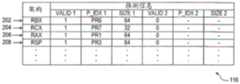
图2是在执行上面列出的指令μop 1和μop 2之后但是执行μop 3之前,根据本发明的一个实施例的重命名表116的至少一部分的图。重命名表116的第一最左边的列列出了用于64位版本的架构(ARCH)寄存器符号,如RAX、RBX、RCX、RSP等所示。尽管仅示出了64位版本,但是应当理解,ARCH符号还可以包括32位版本、16位版本、8位版本等。之后多个列的列表示用于映射到至多列出的每个架构寄存器的物理寄存器的预定最大数量N的推测信息。虽然在各种实施例中可以将附加的物理寄存器映射到每个架构寄存器,但是合并3个或更多个物理寄存器计算上变得复杂(例如,N为3或更多)。在一个实施例中,对第三物理寄存器的部分写入被合并,使得在重命名表116中一次只允许2个映射(例如,N=2)。推测信息包括第一映射物理寄存器的有效值(VALID 1)、物理索引符号(P_IDX 1)和尺寸值(SIZE 1),以及第二映射物理寄存器的有效值(VALID 2)、物理索引符号(P_IDX 2)和尺寸值(SIZE 2)。如果映射有效,则有效值为“1”,否则为“0”。物理寄存器索引符号的格式为PRX,其中“X”是从1到可用物理寄存器总数的数字。尺寸值表示为寄存器存储的有效值的位数。任何条目的短划线符号“-”表示“不关心”或没有条目。FIG. 2 is a diagram of at least a portion of the rename table 116 in accordance with one embodiment of the present invention after execution of the above-listed instructions μop 1 and
如图所示,第一条目202将由索引PR6标识的物理寄存器的64位映射到RBX,并且第二条目204将由索引PR7标识的物理寄存器的32位映射到RCX(或ECX)。假设先前执行的指令将相应的结果存储到用于架构寄存器RBX和RCX的物理寄存器PR6和PR7中。在执行μop 1之后,第三条目206将由索引PR1标识的第一物理寄存器的64位映射到寄存器RAX,其中PR6的内容被移动到PR1。在执行μop 2之后,第三条目206还将由索引PR2标识的第二物理寄存器的32位映射到RAX,其中PR7的内容移动到PR2。因此,应当理解,64位架构寄存器RAX的值包含在两个物理寄存器PR1和PR2中,其中较低或最低有效32位存储在PR2中,并且下一个更高有效32位存储在PR1。第三MOV指令旨在将RAX的内容移动到RSP中。然而,RAX的内容分布在两个不同的物理寄存器PR1和PR2之间,使得μop 3无法从单个物理寄存器获取RAX的完整内容。As shown, the
合并系统122检查包括μop 1-μop 3的指令流,并检测RAX的内容被存储在两个不同物理寄存器中的尺寸问题。合并系统122生成将PR2的内容合并到PR1中的合并(MRG)指令,使得PR1存储RAX的全部内容。插入MRG指令以修改原始指令模式,如下所示:
μop 1)MOV RAX,RBXμop 1) MOV RAX, RBX
μop 2)MOV EAX,ECXμop 2) MOV EAX, ECX
μop M)MRG PR1,PR2,PR1μop M)MRG PR1, PR2, PR1
μop 3)MOV RSP,RAXμop 3) MOV RSP, RAX
其中,在μop3之前插入μopM,并进行操作以将PR2的内容组合到PR1中。合并(MRG)指令的格式μopM包括3个参量或操作数,包括2个源寄存器和1个目标寄存器。前两个操作数PR1和PR2是源操作数,其中第一PR1标识较大结果的源,第二PR2标识较小结果的来源。第三操作数PR1标识合并操作的目的地,其中存储在PR2中的较小结果与存储在PR1中的较大结果合并,并且合并结果被存储回PR1作为目的地寄存器。在μop M执行之后,μop 3可以被执行而不改变,因为物理寄存器PR1存储架构寄存器RAX的完整内容。where μopM is inserted before μop3 and operates to combine the contents of PR2 into PR1. The merge (MRG) instruction format μopM includes 3 arguments or operands, including 2 source registers and 1 destination register. The first two operands PR1 and PR2 are source operands, where the first PR1 identifies the source of the larger result and the second PR2 identifies the source of the smaller result. The third operand PR1 identifies the destination of the merge operation, where the smaller result stored in PR2 is merged with the larger result stored in PR1 and the merged result is stored back to PR1 as the destination register. After μop M is executed,
图3是在执行指令μop 1、μop 2、μop M和μop 3之后根据本发明的一个实施例的重命名表116的至少一部分的图。在执行μop M之后,修改重命名表的条目206,其中VALID 2被改变为“0”,表示RAX仅被映射到一个物理寄存器PR1。在执行μop 3时,另一个物理寄存器PR3被分配给架构寄存器RSP,并且PR1的内容被复制到PR3,如第四条目208所示,其中条目208的值VALID 1、P_IDX 1和SIZE 1为1、PR3和64。此外,VALID 2值可以被设置为“0”,使RSP很清楚得被映射到仅一个物理寄存器PR3。虽然指令μop 1、μop 2和μop 3是“移动”指令,但是它们可以被实现为“复制”操作,其中RBX、RCX和RAX的内容在执行四个指令之后保持有效,如重命名表116所示。FIG. 3 is a diagram of at least a portion of the rename table 116 in accordance with one embodiment of the present invention after execution of the instructions μop 1 ,
上述示例示出了在尝试读取分布在多个(例如,2个)物理寄存器之间的架构寄存器的读取指令之前插入合并指令。合并指令将多个物理寄存器的内容合并到一个寄存器中,以使读取指令成功操作。考虑μop 3是另一个部分写操作的情况,例如MOV AX,DX,其中第二部分写入变成架构寄存器RAX的低16位。在一个实施例(未示出)中,重命名表116可以包括用于存储RAX的第三部分写入结果的第三组有效索引和尺寸条目。第三物理寄存器PR3可用于将第二部分写入的低16位结果存储到RAX。将3个或更多的物理寄存器映射到一个架构寄存器可能在某些配置中计算复杂。如图4所示,对于其中仅包括每个架构寄存器的2个映射(例如,N=2)的示出的实施例,以先前描述的相同方式在第二部分写指令之前插入合并指令μop M并以与图1中的条目206所示相同的方式组合寄存器PR1和PR2的内容到PR1。然后,对于条目206,VALID 2值被改变为“1”,P_IDX 2值被改变为PR3,并且SIZE 2被改变为16,使得RAX仍被映射到仅2个物理寄存器,PR1和PR3。The above example shows inserting a merge instruction prior to a read instruction attempting to read an architectural register distributed among multiple (eg, 2) physical registers. The merge instruction merges the contents of multiple physical registers into a single register for the read instruction to operate successfully. Consider the case where
总而言之,合并系统122产生合并指令以当指令尝试从映射到多个物理寄存器的架构寄存器读取时执行读合并,或者当指令尝试执行额外的部分写入时执行写合并到已经映射到最大数量的物理寄存器的架构寄存器。写合并用于防止映射超过同一架构寄存器(及其部分)的物理寄存器的最大数量,并且读合并用于将多个物理寄存器的内容合并到一个物理寄存器,以使随后的读取指令进行适当的操作。In summary, the coalescing
图4是根据本发明的一个实施例的图1的重命名表的至少一部分的图。其中仅包括每个架构寄存器的2个映射,并且其中与上述相同的方式将合并指令μopM在第二部分写指令之前插入以便以与图3中的条目206所示相同的方式将寄存器PR1和PR2的内容组合到PR1。FIG. 4 is a diagram of at least a portion of the rename table of FIG. 1 according to one embodiment of the present invention. where only 2 mappings for each architectural register are included, and where the merge instruction μopM is inserted before the second partial write instruction in the same manner as above to merge registers PR1 and PR2 in the same manner as shown in
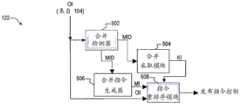
图5是示出根据本发明的一个实施例实现的合并系统122的框图。指令转换器104向RAT 106提供的原始指令(OI)被提供给合并检测器502和指令重排序模块508。在一个实施例中,指令转换器104每时钟周期一次提供至多达四个μops。合并检测器502分析与每个接收到的μop的源和目的地相对应的架构寄存器,并且确定是否有任何架构寄存器需要合并。在一个实施例中,每个μops可以具有至多达3个源和1个目的地,使得每个周期可以存在至多达16个合并,对于四个接收的μops中的每一个可以有4个合并。合并检测器502形成合并标识符(MID),并提供MID到合并采取模块504和合并指令生成器506。MID标识需要被合并的至多达4个接收的μops的每个架构寄存器。Figure 5 is a block diagram illustrating a
合并指令生成器506接收MID,读取重命名表116中的信息以标识需要合并的架构寄存器,并为每个要合并的架构寄存器生成相应的合并指令。如前所述,合并指令MRG标识映射到架构寄存器的对应物理寄存器,并将该信息合并到存储较大值的物理寄存器,例如,μopM将PR1和PR2合并到映射到架构寄存器EAX的PR1中。合并指令生成器506将一个或多个合并指令(MI)输出到指令重排序模块508。The
合并采取模块504接收MID并确定在从指令转换器104接收到的每个原始μop之前应该插入的合并μops的数量。合并采取模块504然后根据多个采用规则之一分割原始μops并且向指令重排序模块508输出终止指示(KI),以便在每个时钟周期中标识应从RAT 106向RS 108发布哪些原始指令。术语“终止”表示相对于当前时钟周期的终止,以标识被推入下一个时钟周期的下一个指令。在一个实施例中,RAT 106一次向包括合并μops的RS 108发布至多达4μops。如本文进一步描述的,可以定义多个采用规则,以提供定时和性能之间的不同折衷。合并采取模块504可以在不同的采取规则之间切换以确保适当的定时和/或实现一定程度的性能。Merge
指令重排序模块508与KI一起接收原始指令OI和合并指令MI,并提供确定每个时钟周期发布原始和合并μops中的哪一个的发布指令控制。The
图6是示出根据本发明的另一实施例实现的合并系统122的框图。指令转换器104向RAT 106提供的原始指令(OI)被提供给合并检测器502和指令重排序模块608,指令重排序模块608以与指令重排序模块508类似的方式操作。合并检测器502以基本上相同的方式将MID提供给合并采取模块504,其以类似的方式开发KI。然而,KI被提供给也接收原始指令OI的指令移位器610。指令移位器610根据KI移位原始μops,以确定每个时钟周期哪个μop被移位到时隙0。合并指令生成器506通过接收MID并将合并指令MI提供给指令重排序模块608而以类似的方式操作。指令移位器610与合并指令生成器506和指令重排序模块608配合,以提供确定每个时钟周期发布原始和合并的μops中的哪一个的指令控制。FIG. 6 is a block diagram illustrating a
图7是示出根据本发明的实施例的示例性采取规则的示意图。一组4μop指令702,如I1、I2、3和I4所示,按照程序顺序由指令转换器104提供给RAT 106。合并系统122对指令I1-I4执行合并检查,并产生合并指令M2和M3。合并系统122将合并指令M2和M3插入到原始指令组702中以提供经修改的指令组706。在这种情况下,对应于I2的M2被插入在I2之前,对应于I3的M3被插入到I3之前,使得指令流被改变为I1、M2、I2、M3、I3和I4。合并系统122进一步使用一个或多个采取规则中的一个选择的规则来确定为每个时钟周期发布哪个指令。采取规则不改变指令流706的顺序,而是确定在当前周期中发布哪些指令并将其推送到下一个周期。FIG. 7 is a schematic diagram illustrating an exemplary adoption rule according to an embodiment of the present invention. A set of 4[mu]
对于三种不同的采取规则中的每一个示出了四个连续的时钟周期T1、T2、T3和T4。第一行显示被称为“单独发布合并(ISSUE MERGE ALONE)”710的第一采取规则,第二行显示被称为“发布直到合并(ISSUE UNTIL MERGE)”712的第二采取规则,第三行示出被称为“发布直到第二合并(ISSUE UNTIL 2ND MERGE)”714的第三采取规则。如前所述,合并采取模块504基于由合并检测器502提供的MID施加合并取得规则中的活动的一个以提供用于标识在每个时钟周期中发布的指令的KI。不同的采取规则提供了时间和性能之间的折衷,并且可以基于操作参数进行切换。在每个时钟周期中,当然,指令转换器104可以继续提供至多4个附加指令(未示出)。时序考虑了由合并检测器502执行的功能,以分析输入指令进而提供MID,以及考虑了由合并指令生成器506执行的功能,以生成要插入到指令流中的期望的合并指令。Four consecutive clock cycles T1, T2, T3 and T4 are shown for each of the three different taking rules. The first row shows the first take rule called "ISSUE MERGE ALONE" 710, the second row shows the second take rule called "ISSUE UNTIL MERGE" 712, the third The row shows a third take rule called "ISSUE UNTIL 2ND MERGE" 714 . As previously mentioned, the merge-
ISSUE MERGE ALONE 710确定需要合并的原始指令以及它们对应的合并指令将在每个周期中单独发布。指令I1不需要合并,并且首先分配给T1周期。由于指令I2需要合并,所以将其与合并指令M2一起被推到第二周期T2,从而在周期T2中单独发布指令M2和I2。然后由于指令I3需要合并,所以它与其合并指令M3一起被推到第三周期,所以在周期T3中单独发布指令M3和I3。不需要合并的指令I4在第四周期T4中发布。虽然未示出,但是根据是否需要合并,可以在周期T4中的指令I4之后最多发布3个附加指令。在这种情况下,需要4个时钟周期来发布ISSUE MERGE ALONE710的指令流706。ISSUE MERGE ALONE 710 determines that the original instructions that need to be merged and their corresponding merged instructions will be issued separately in each cycle. Instruction I1 does not need to be merged and is allocated to the T1 cycle first. Since instruction I2 needs to be merged, it is pushed to the second cycle T2 along with the merged instruction M2, so that instructions M2 and I2 are issued separately in cycle T2. Then since instruction I3 needs to be merged, it is pushed to the third cycle along with its merged instruction M3, so instructions M3 and I3 are issued separately in cycle T3. The instruction I4 that does not require merging is issued in the fourth cycle T4. Although not shown, up to 3 additional instructions may be issued after instruction I4 in cycle T4, depending on whether coalescing is required. In this case, 4 clock cycles are required to issue the
ISSUE UNTIL MERGE 712发布至多每个周期中允许的总数(如4)的指令,并发布指令直到指令及其所有相应的合并指令已经在该周期中发布。在这种情况下,由于指令I1不需要合并,但是指令I2仅仅只需要一个合并指令M2,所以在第一周期T1中发布指令I1、M2和I2。下一条指令I3也需要合并,因此在下一个周期T2中发布指令M3和I3。虽然未示出,但是如果I3除了M3之外还有更多的合并指令,如果T2中发布的总数不超过最大数量(如4),则它们也可以在T2内发布。这留下了在第三周期T3中发布的指令I4。再次,根据是否需要合并并且如果可以满足时序,可以在周期T3中可以与指令I4一起发布至多3个附加指令(未示出)。在这种情况下,需要3个时钟周期来发布指令流706,其中ISSUE UNTIL MERGE 712以较少的时钟周期发布指令流706作为ISSUE MERGE ALONE 710,从而提高性能。ISSUE UNTIL MERGE 712 issues instructions up to the total allowed in each cycle (eg, 4), and issues instructions until the instruction and all its corresponding merged instructions have been issued in that cycle. In this case, since the instruction I1 does not need to be merged, but the instruction I2 only needs one merged instruction M2, the instructions I1, M2 and I2 are issued in the first cycle T1. The next instruction I3 also needs to be merged, so the instructions M3 and I3 are issued in the next cycle T2. Although not shown, if I3 has more merge instructions in addition to M3, they can also be issued within T2 if the total number issued in T2 does not exceed the maximum number (eg, 4). This leaves the instruction I4 issued in the third cycle T3. Again, up to 3 additional instructions (not shown) may be issued in cycle T3 along with instruction I4, depending on whether merging is required and if timing can be met. In this case, 3 clock cycles are required to issue
ISSUE UNTIL 2ND MERGE 714发布每个周期中允许的至多总数(如4)的指令,并且发布指令,直到指令、其所有相应的合并指令和所有其他指令指令在对应于下一个指令的下一个合并指令之前已在周期中发布为止。然而,在第一周期T1中,指令M3和I3不能与M2和I2一起发布,因为在所示配置中每个周期只允许最多4个指令。以这种方式,指令M3和I3被推到下一个周期T2。由于指令I4不需要合并,所以也可以包括在周期T2中。虽然未示出,但是如果附加指令不需要合并,并且如果定时允许,就如T2中发布的总数不超过最大数4,则在周期T2中可以发布一个附加指令。因此,ISSUE UNTIL 2ND MERGE 714通过仅在两个周期内发布指令流706而提供比其他采取规则更大的性能,但是可能提出额外的时序挑战。ISSUE UNTIL 2ND MERGE 714 Issue up to the total number of instructions allowed in each cycle (eg 4) and issue instructions until the instruction, all its corresponding merged instructions and all other instruction instructions are merged in the next corresponding to the next instruction Instructions have previously been issued in the cycle. However, in the first cycle T1, instructions M3 and I3 cannot be issued together with M2 and I2 because only a maximum of 4 instructions per cycle are allowed in the configuration shown. In this way, instructions M3 and I3 are pushed to the next cycle T2. Since instruction I4 does not need to be merged, it can also be included in cycle T2. Although not shown, one additional instruction may be issued in cycle T2 if additional instructions do not need to be merged, and if timing permits, such as the total number issued in T2 does not exceed the maximum number of 4. Thus, ISSUE UNTIL 2ND MERGE 714 provides greater performance than other take rules by issuing
已经提出了前述描述,以使本领域普通技术人员能够在特定应用及其要求的背景下提供和使用本发明。虽然已经参考其某些优选的形式相当详细地描述了本发明,但是其他的形式和变化是可能的和预期的。对优选实施例的各种修改对于本领域技术人员将是显而易见的,并且本文定义的一般原理可以应用于其他实施例。例如,本文描述的方框可以以包括逻辑器件或电路等的任何合适的方式来实现。本领域技术人员应当理解,在不脱离本发明的精神和范围的情况下,它们可以容易地使用所公开的概念和具体实施例作为设计或修改用于实现本发明的相同目的的其他结构的基础。因此,本发明不旨在限于本文所示和所述的具体实施例,而是符合与本文公开的原理和新颖特征一致的最广范围。The foregoing description has been presented to enable one of ordinary skill in the art to make and use the present invention in the context of a particular application and its requirements. While the present invention has been described in considerable detail with reference to some of its preferred forms, other forms and variations are possible and contemplated. Various modifications to the preferred embodiment will be readily apparent to those skilled in the art, and the generic principles defined herein may be applied to other embodiments. For example, the blocks described herein may be implemented in any suitable manner including logic devices or circuits, or the like. Those skilled in the art should appreciate that they may readily use the disclosed conception and specific embodiment as a basis for designing or modifying other structures for carrying out the same purposes of the present invention without departing from the spirit and scope of the invention . Therefore, the present invention is not intended to be limited to the specific embodiments shown and described herein, but is to be accorded the widest scope consistent with the principles and novel features disclosed herein.
Claims (19)
Priority Applications (3)
| Application Number | Priority Date | Filing Date | Title |
|---|---|---|---|
| CN201710491888.7ACN107291425B (en) | 2017-06-23 | 2017-06-23 | System and method for incorporating partially written results that resolve renaming size issues |
| US15/810,876US10853080B2 (en) | 2017-06-23 | 2017-11-13 | System and method of merging partial write results for resolving renaming size issues |
| TW107107036ATWI666587B (en) | 2017-06-23 | 2018-03-02 | Processor and method of merging partial write results for resolving renaming size issues of the processor |
Applications Claiming Priority (1)
| Application Number | Priority Date | Filing Date | Title |
|---|---|---|---|
| CN201710491888.7ACN107291425B (en) | 2017-06-23 | 2017-06-23 | System and method for incorporating partially written results that resolve renaming size issues |
Publications (2)
| Publication Number | Publication Date |
|---|---|
| CN107291425A CN107291425A (en) | 2017-10-24 |
| CN107291425Btrue CN107291425B (en) | 2020-11-24 |
Family
ID=60099789
Family Applications (1)
| Application Number | Title | Priority Date | Filing Date |
|---|---|---|---|
| CN201710491888.7AActiveCN107291425B (en) | 2017-06-23 | 2017-06-23 | System and method for incorporating partially written results that resolve renaming size issues |
Country Status (3)
| Country | Link |
|---|---|
| US (1) | US10853080B2 (en) |
| CN (1) | CN107291425B (en) |
| TW (1) | TWI666587B (en) |
Families Citing this family (2)
| Publication number | Priority date | Publication date | Assignee | Title |
|---|---|---|---|---|
| US11494190B2 (en)* | 2021-03-31 | 2022-11-08 | Arm Limited | Circuitry and method for controlling a generated association of a physical register with a predicated processing operation based on predicate data state |
| CN115016848A (en)* | 2022-05-31 | 2022-09-06 | 上海阵量智能科技有限公司 | Instruction processing method, device, chip, board, device and medium |
Citations (6)
| Publication number | Priority date | Publication date | Assignee | Title |
|---|---|---|---|---|
| US6463525B1 (en)* | 1999-08-16 | 2002-10-08 | Sun Microsystems, Inc. | Merging single precision floating point operands |
| US7840783B1 (en)* | 2007-09-10 | 2010-11-23 | Netlogic Microsystems, Inc. | System and method for performing a register renaming operation utilizing hardware which is capable of operating in at least two modes utilizing registers of multiple widths |
| CN101794214B (en)* | 2009-02-04 | 2013-11-20 | 世意法(北京)半导体研发有限责任公司 | Register renaming system using multi-block physical register mapping table and method thereof |
| CN104049947A (en)* | 2013-03-15 | 2014-09-17 | 三星电子株式会社 | Dynamic Rename Based Register Reconfiguration Of A Vector Register File |
| CN106095393A (en)* | 2016-06-22 | 2016-11-09 | 上海兆芯集成电路有限公司 | The system and method for partial write result is merged during retraction phase |
| US9569574B1 (en)* | 2014-03-07 | 2017-02-14 | Altera Corporation | Method and apparatus for performing fast incremental physical design optimization |
Family Cites Families (12)
| Publication number | Priority date | Publication date | Assignee | Title |
|---|---|---|---|---|
| US7228403B2 (en)* | 2000-12-23 | 2007-06-05 | International Business Machines Corporation | Method for handling 32 bit results for an out-of-order processor with a 64 bit architecture |
| GB2393270B (en)* | 2002-09-19 | 2005-07-27 | Advanced Risc Mach Ltd | Executing variable length instructions stored within a plurality of discrete memory address regions |
| CN100555225C (en)* | 2008-03-17 | 2009-10-28 | 中国科学院计算技术研究所 | A kind of risc processor device and method of supporting the X86 virtual machine |
| US7937561B2 (en)* | 2008-04-03 | 2011-05-03 | Via Technologies, Inc. | Merge microinstruction for minimizing source dependencies in out-of-order execution microprocessor with variable data size macroarchitecture |
| TWI418991B (en)* | 2010-06-03 | 2013-12-11 | Super Talent Electronics Inc | Usb-attached-scsi flash-memory system with additional command, status, and control pipes to a smart-storage switch |
| US20120059866A1 (en)* | 2010-09-03 | 2012-03-08 | Advanced Micro Devices, Inc. | Method and apparatus for performing floating-point division |
| WO2013081596A1 (en)* | 2011-11-30 | 2013-06-06 | Intel Corporation | Efficient implementation of rsa using gpu/cpu architecture |
| WO2013095401A1 (en)* | 2011-12-20 | 2013-06-27 | Intel Corporation | System and method for out-of-order prefetch instructions in an in-order pipeline |
| US9098265B2 (en)* | 2012-07-11 | 2015-08-04 | Arm Limited | Controlling an order for processing data elements during vector processing |
| JP6511462B2 (en)* | 2013-10-27 | 2019-05-15 | アドバンスト・マイクロ・ディバイシズ・インコーポレイテッドAdvanced Micro Devices Incorporated | Processor and method for floating point register aliasing |
| US10318299B2 (en)* | 2013-10-31 | 2019-06-11 | International Business Machines Corporation | Reading a register pair by writing a wide register |
| US9442731B2 (en)* | 2014-03-13 | 2016-09-13 | Intel Corporation | Packed two source inter-element shift merge processors, methods, systems, and instructions |
- 2017
- 2017-06-23CNCN201710491888.7Apatent/CN107291425B/enactiveActive
- 2017-11-13USUS15/810,876patent/US10853080B2/enactiveActive
- 2018
- 2018-03-02TWTW107107036Apatent/TWI666587B/enactive
Patent Citations (6)
| Publication number | Priority date | Publication date | Assignee | Title |
|---|---|---|---|---|
| US6463525B1 (en)* | 1999-08-16 | 2002-10-08 | Sun Microsystems, Inc. | Merging single precision floating point operands |
| US7840783B1 (en)* | 2007-09-10 | 2010-11-23 | Netlogic Microsystems, Inc. | System and method for performing a register renaming operation utilizing hardware which is capable of operating in at least two modes utilizing registers of multiple widths |
| CN101794214B (en)* | 2009-02-04 | 2013-11-20 | 世意法(北京)半导体研发有限责任公司 | Register renaming system using multi-block physical register mapping table and method thereof |
| CN104049947A (en)* | 2013-03-15 | 2014-09-17 | 三星电子株式会社 | Dynamic Rename Based Register Reconfiguration Of A Vector Register File |
| US9569574B1 (en)* | 2014-03-07 | 2017-02-14 | Altera Corporation | Method and apparatus for performing fast incremental physical design optimization |
| CN106095393A (en)* | 2016-06-22 | 2016-11-09 | 上海兆芯集成电路有限公司 | The system and method for partial write result is merged during retraction phase |
Also Published As
| Publication number | Publication date |
|---|---|
| CN107291425A (en) | 2017-10-24 |
| US20180373539A1 (en) | 2018-12-27 |
| TW201905681A (en) | 2019-02-01 |
| US10853080B2 (en) | 2020-12-01 |
| TWI666587B (en) | 2019-07-21 |
Similar Documents
| Publication | Publication Date | Title |
|---|---|---|
| US5699537A (en) | Processor microarchitecture for efficient dynamic scheduling and execution of chains of dependent instructions | |
| CN106648843B (en) | System, method and apparatus for improving throughput of contiguous transactional memory regions | |
| US7822951B2 (en) | System and method of load-store forwarding | |
| EP3314437B1 (en) | Verifying branch targets in a block based processor | |
| US9092215B2 (en) | Mapping between registers used by multiple instruction sets | |
| US7937561B2 (en) | Merge microinstruction for minimizing source dependencies in out-of-order execution microprocessor with variable data size macroarchitecture | |
| US6505293B1 (en) | Register renaming to optimize identical register values | |
| US6594754B1 (en) | Mapping destination logical register to physical register storing immediate or renamed source register of move instruction and using mapping counters | |
| JP7156776B2 (en) | System and method for merging partial write results during retirement phase | |
| US6351804B1 (en) | Control bit vector storage for a microprocessor | |
| US20020133682A1 (en) | System with wide operand architecture, and method | |
| US9471325B2 (en) | Method and apparatus for selective renaming in a microprocessor | |
| US9454371B2 (en) | Micro-architecture for eliminating MOV operations | |
| JP2008537231A (en) | System and method in which conditional instructions provide output unconditionally | |
| EP3060979B1 (en) | Processor and methods for immediate handling and flag handling | |
| US6266763B1 (en) | Physical rename register for efficiently storing floating point, integer, condition code, and multimedia values | |
| US7406587B1 (en) | Method and system for renaming registers in a microprocessor | |
| US9081581B2 (en) | Size mis-match hazard detection | |
| US10248425B2 (en) | Processor with slave free list that handles overflow of recycled physical registers and method of recycling physical registers in a processor using a slave free list | |
| CN107291425B (en) | System and method for incorporating partially written results that resolve renaming size issues | |
| US6237076B1 (en) | Method for register renaming by copying a 32 bits instruction directly or indirectly to a 64 bits instruction | |
| US20050102494A1 (en) | Method and apparatus for register stack implementation using micro-operations | |
| US7783692B1 (en) | Fast flag generation | |
| CN120687145A (en) | Instruction processing method, device and related equipment |
Legal Events
| Date | Code | Title | Description |
|---|---|---|---|
| PB01 | Publication | ||
| PB01 | Publication | ||
| SE01 | Entry into force of request for substantive examination | ||
| SE01 | Entry into force of request for substantive examination | ||
| GR01 | Patent grant | ||
| GR01 | Patent grant | ||
| CP03 | Change of name, title or address | ||
| CP03 | Change of name, title or address | Address after:Room 301, 2537 Jinke Road, Zhangjiang High Tech Park, Pudong New Area, Shanghai 201203 Patentee after:Shanghai Zhaoxin Semiconductor Co.,Ltd. Address before:Room 301, 2537 Jinke Road, Zhangjiang hi tech park, Shanghai 201203 Patentee before:VIA ALLIANCE SEMICONDUCTOR Co.,Ltd. |