CN107229577B - Storage system and operation method thereof - Google Patents
Storage system and operation method thereofDownload PDFInfo
- Publication number
- CN107229577B CN107229577BCN201610269575.2ACN201610269575ACN107229577BCN 107229577 BCN107229577 BCN 107229577BCN 201610269575 ACN201610269575 ACN 201610269575ACN 107229577 BCN107229577 BCN 107229577B
- Authority
- CN
- China
- Prior art keywords
- metapage
- metapages
- superblock
- die
- location
- Prior art date
- Legal status (The legal status is an assumption and is not a legal conclusion. Google has not performed a legal analysis and makes no representation as to the accuracy of the status listed.)
- Active
Links
Images


Classifications
- G—PHYSICS
- G06—COMPUTING OR CALCULATING; COUNTING
- G06F—ELECTRIC DIGITAL DATA PROCESSING
- G06F12/00—Accessing, addressing or allocating within memory systems or architectures
- G06F12/02—Addressing or allocation; Relocation
- G06F12/08—Addressing or allocation; Relocation in hierarchically structured memory systems, e.g. virtual memory systems
- G06F12/10—Address translation
- G06F12/1009—Address translation using page tables, e.g. page table structures
- G—PHYSICS
- G06—COMPUTING OR CALCULATING; COUNTING
- G06F—ELECTRIC DIGITAL DATA PROCESSING
- G06F3/00—Input arrangements for transferring data to be processed into a form capable of being handled by the computer; Output arrangements for transferring data from processing unit to output unit, e.g. interface arrangements
- G06F3/06—Digital input from, or digital output to, record carriers, e.g. RAID, emulated record carriers or networked record carriers
- G06F3/0601—Interfaces specially adapted for storage systems
- G06F3/0628—Interfaces specially adapted for storage systems making use of a particular technique
- G06F3/0638—Organizing or formatting or addressing of data
- G06F3/064—Management of blocks
- G—PHYSICS
- G06—COMPUTING OR CALCULATING; COUNTING
- G06F—ELECTRIC DIGITAL DATA PROCESSING
- G06F3/00—Input arrangements for transferring data to be processed into a form capable of being handled by the computer; Output arrangements for transferring data from processing unit to output unit, e.g. interface arrangements
- G06F3/06—Digital input from, or digital output to, record carriers, e.g. RAID, emulated record carriers or networked record carriers
- G06F3/0601—Interfaces specially adapted for storage systems
- G06F3/0602—Interfaces specially adapted for storage systems specifically adapted to achieve a particular effect
- G06F3/061—Improving I/O performance
- G—PHYSICS
- G06—COMPUTING OR CALCULATING; COUNTING
- G06F—ELECTRIC DIGITAL DATA PROCESSING
- G06F3/00—Input arrangements for transferring data to be processed into a form capable of being handled by the computer; Output arrangements for transferring data from processing unit to output unit, e.g. interface arrangements
- G06F3/06—Digital input from, or digital output to, record carriers, e.g. RAID, emulated record carriers or networked record carriers
- G06F3/0601—Interfaces specially adapted for storage systems
- G06F3/0668—Interfaces specially adapted for storage systems adopting a particular infrastructure
- G06F3/0671—In-line storage system
- G06F3/0673—Single storage device
- G06F3/0679—Non-volatile semiconductor memory device, e.g. flash memory, one time programmable memory [OTP]
- G—PHYSICS
- G06—COMPUTING OR CALCULATING; COUNTING
- G06F—ELECTRIC DIGITAL DATA PROCESSING
- G06F3/00—Input arrangements for transferring data to be processed into a form capable of being handled by the computer; Output arrangements for transferring data from processing unit to output unit, e.g. interface arrangements
- G06F3/06—Digital input from, or digital output to, record carriers, e.g. RAID, emulated record carriers or networked record carriers
- G06F3/0601—Interfaces specially adapted for storage systems
- G06F3/0668—Interfaces specially adapted for storage systems adopting a particular infrastructure
- G06F3/0671—In-line storage system
- G06F3/0683—Plurality of storage devices
- G06F3/0688—Non-volatile semiconductor memory arrays
- G—PHYSICS
- G11—INFORMATION STORAGE
- G11C—STATIC STORES
- G11C16/00—Erasable programmable read-only memories
- G11C16/02—Erasable programmable read-only memories electrically programmable
- G11C16/06—Auxiliary circuits, e.g. for writing into memory
- G11C16/08—Address circuits; Decoders; Word-line control circuits
- G—PHYSICS
- G06—COMPUTING OR CALCULATING; COUNTING
- G06F—ELECTRIC DIGITAL DATA PROCESSING
- G06F2212/00—Indexing scheme relating to accessing, addressing or allocation within memory systems or architectures
- G06F2212/72—Details relating to flash memory management
- G06F2212/7207—Details relating to flash memory management management of metadata or control data
Landscapes
- Engineering & Computer Science (AREA)
- Theoretical Computer Science (AREA)
- Physics & Mathematics (AREA)
- General Engineering & Computer Science (AREA)
- General Physics & Mathematics (AREA)
- Human Computer Interaction (AREA)
- Techniques For Improving Reliability Of Storages (AREA)
Abstract
Translated fromChinese
Description
Translated fromChinese相关申请的交叉引用CROSS-REFERENCE TO RELATED APPLICATIONS
本申请要求2016年3月25日提交的第15/081,644号美国非临时申请的优先权,其全部内容通过引用合并于此。This application claims priority to US Non-Provisional Application No. 15/081,644, filed March 25, 2016, the entire contents of which are incorporated herein by reference.
技术领域technical field
本公开的示例性实施例涉及一种存储系统及其操作方法。Exemplary embodiments of the present disclosure relate to a storage system and an operating method thereof.
背景技术Background technique
计算机环境范式已经变为可以随时随地使用的普适计算系统。由于这个原因,诸如移动电话、数字相机和笔记本电脑的便携式电子设备的使用已快速增加。这些便携式电子设备通常使用具有存储器件的存储系统(即,数据储存设备)。该数据储存设备被用作便携式电子设备的主存储设备或辅助存储设备。The computing environment paradigm has become a ubiquitous computing system that can be used anytime, anywhere. For this reason, the use of portable electronic devices such as mobile phones, digital cameras and notebook computers has rapidly increased. These portable electronic devices typically use storage systems (ie, data storage devices) with storage devices. The data storage device is used as a primary or secondary storage device for the portable electronic device.
由于使用存储器件的数据储存设备无活动部件,因此它们提供优异的稳定性、耐久性、高信息访问速度和低功耗。具有这些优点的数据储存设备的示例包括通用串行总线(USB)存储器件、具有各种接口的存储卡以及固态驱动器(SSD)。Since data storage devices using memory devices have no moving parts, they provide excellent stability, durability, high information access speed, and low power consumption. Examples of data storage devices with these advantages include Universal Serial Bus (USB) memory devices, memory cards with various interfaces, and solid state drives (SSD).
发明内容SUMMARY OF THE INVENTION
本发明的方面包括一种存储系统。该存储系统可以包括:存储器件,所述存储器件具有多个裸片、第一超级块以及第二超级块,第一超级块包括储存在裸片上的位置处的第一元页,而第二超级块包括储存在裸片上的位置处的第二元页;以及控制器,所述控制器适用于读取这些超级块中的元页,其中,第一元页的储存位置与第二元页的储存位置错开,使得在单个读取期间通过控制器读取第一元页和第二元页。Aspects of the invention include a storage system. The storage system may include a storage device having a plurality of dies, a first superblock including a first metapage stored at a location on the die, and a second superblock, and a second superblock superblocks include second metapages stored at locations on the die; and a controller adapted to read metapages in these superblocks, wherein the storage location of the first metapage is the same as the second metapage The storage locations are staggered so that the first and second metapages are read by the controller during a single read.
本发明的其他方面包括一种方法,该方法包括:将与第一超级块相对应的第一元页储存在裸片上的位置处;将与第二超级块相对应的第二元页储存在裸片上的位置处,使得第一元页的储存位置与第二元页的储存位置错开;以及在单个读取期间读取第一元页和第二元页。Other aspects of the invention include a method comprising: storing a first metapage corresponding to a first superblock at a location on a die; storing a second metapage corresponding to a second superblock in a at a location on the die such that the storage location of the first metapage is staggered from the storage location of the second metapage; and the first metapage and the second metapage are read during a single read.
本发明的进一步的方面包括一种存储器件。该存储器件可以包括多个裸片以及多个超级块,所述多个超级块中的每个包括在多个裸片中的裸片上的位置处储存的元页,其中,这些元页中的每个的储存位置彼此错开,使得在单个读取命令期间读取这些元页中的每个。A further aspect of the invention includes a memory device. The memory device may include a plurality of dies and a plurality of superblocks, each of the plurality of superblocks including metapages stored at locations on the die of the plurality of dies, wherein the metapages of the metapages are The storage locations of each are staggered from each other so that each of these metapages is read during a single read command.
附图说明Description of drawings
图1是示意性地图示根据本发明的一个实施例的存储系统的框图。FIG. 1 is a block diagram schematically illustrating a storage system according to one embodiment of the present invention.
图2是图示根据本发明的一个实施例的存储系统的框图。2 is a block diagram illustrating a storage system according to one embodiment of the present invention.
图3是图示根据本发明的一个实施例的存储器件的存储块的电路图。FIG. 3 is a circuit diagram illustrating a memory block of a memory device according to one embodiment of the present invention.
图4是图示根据本发明的一个实施例的存储器控制器的控制单元的示图。FIG. 4 is a diagram illustrating a control unit of a memory controller according to one embodiment of the present invention.
图5是根据本发明的若干方面的存储系统的框图。5 is a block diagram of a storage system in accordance with aspects of the present invention.
图6A和图6B是根据本发明的若干方面的超级块和裸片的示图。6A and 6B are diagrams of superblocks and dies in accordance with aspects of the present disclosure.
图7是对超级块执行的读取的示图。7 is a diagram of a read performed on a superblock.
图8是根据本发明的若干方面的用于储存元页和执行SPOR过程的步骤的流程图。8 is a flowchart of steps for storing a metapage and performing a SPOR process in accordance with aspects of the present disclosure.
图9是根据本发明的若干方面的超级块的示图。9 is a diagram of a superblock in accordance with aspects of the present disclosure.
图10是根据本发明的若干方面执行的读取的示图。10 is an illustration of a read performed in accordance with aspects of the present invention.
具体实施方式Detailed ways
下面将参照附图来更详细地描述各种实施例。然而,本发明可以以不同的形式实施,而不应当被解释为局限于本文中所阐述的实施例。相反地,这些实施例被提供使得本公开将是彻底和完整的,且这些实施例将把本发明的范围充分传达给本领域技术人员。贯穿本公开,相同的附图标记在本发明的各种附图和实施例中始终指代相同的部分。Various embodiments will be described in more detail below with reference to the accompanying drawings. The present invention may, however, be embodied in different forms and should not be construed as limited to the embodiments set forth herein. Rather, these embodiments are provided so that this disclosure will be thorough and complete, and will fully convey the scope of the invention to those skilled in the art. Throughout this disclosure, the same reference numbers refer to the same parts throughout the various figures and embodiments of the invention.
本发明可以以各种方式来实施,包括作为:过程;装置;系统;物的组合;在计算机可读储存介质上实施的计算机程序产品;和/或处理器(诸如适用于运行储存在耦接至该处理器的存储器上的指令和/或由耦接至该处理器的存储器提供的指令的处理器)。在此说明书中,这些实施方式或本发明可以采用的任何其他形式可以被称作技术。一般而言,在本发明的范围之内可以改变所公开的过程的步骤的次序。除非另外说明,否则被描述为适用于执行任务的组件(诸如处理器或存储器)可以被实施为暂时适用于在给定时间执行该任务的常规组件或被制造用来执行该任务的专用组件。如本文中所用,术语“处理器”指适用于处理数据(诸如计算机程序指令)的一个或更多个器件、电路和/或处理核。The present invention can be implemented in various ways, including as: a process; an apparatus; a system; a combination of things; a computer program product embodied on a computer-readable storage medium; to instructions on the processor's memory and/or instructions provided by the processor's memory coupled to the processor). In this specification, these implementations, or any other form that the invention may take, may be referred to as techniques. In general, the order of the steps of the disclosed processes may be varied within the scope of the invention. Unless otherwise stated, a component described as suitable for performing a task, such as a processor or memory, may be implemented as a conventional component temporarily adapted to perform the task at a given time or a special purpose component manufactured to perform the task. As used herein, the term "processor" refers to one or more devices, circuits, and/or processing cores suitable for processing data, such as computer program instructions.
下面与图示本发明的原理的附图一起提供对本发明的一个或更多个实施例的详细描述。虽然关联这些实施例来描述本发明,但本发明不局限于任何实施例。本发明的范围仅由权利要求来限制,且本发明包括若干替代、变型和等同。在下面的描述中阐述了若干具体细节以提供对本发明的透彻理解。提供这些细节出于示例的目的,且可以在无这些具体细节中的一些或全部的情况下根据权利要求来实践本发明。为了清楚的目的,未详细描述与本发明相关的技术领域中已知的技术材料,使得本发明不被不必要地混淆。A detailed description of one or more embodiments of the invention is provided below along with accompanying drawings that illustrate the principles of the invention. Although the invention is described in relation to these embodiments, the invention is not limited to any embodiment. The scope of the invention is limited only by the claims, and the invention includes several alternatives, modifications and equivalents. In the following description, several specific details are set forth in order to provide a thorough understanding of the present invention. These details are provided for the purpose of example and the invention may be practiced according to the claims without some or all of these specific details. For the purpose of clarity, technical material that is known in the technical fields related to the invention has not been described in detail so that the present invention is not unnecessarily obscured.
与硬盘不同,存储器件(诸如快闪存储器)的“写入前擦除”限制需要系统软件中的被称作闪存转换层(FTL)的特殊层来仿真用于向后兼容性(backward compatibility)的块器件接口。文件系统和应用程序可以使用快闪存储器就好像它们在使用硬盘一样。被认为是逻辑块寻址(LBA)的逻辑至物理(L2P)映射系统是FTL的一部分。Unlike hard disks, the "erase-before-write" limitation of storage devices (such as flash memory) requires a special layer in system software called the Flash Translation Layer (FTL) to emulate for backward compatibility block device interface. File systems and applications can use flash memory as if they were using the hard disk. A logical-to-physical (L2P) mapping system known as Logical Block Addressing (LBA) is part of FTL.
由于用于FTL或LBA的表(在下文中为LBA表)可以在作为易失性存储器的动态随机存取存储器(DRAM)中,因此当出现突然断电时,LBA表将丢失,这导致数据丢失。为了防止数据丢失,固件必须能够在电源接通时重建最新表。如此频繁地将LBA表写入至存储器件(例如,与非快闪存储器)将导致严重的写入性能退化。在有限性能退化的情况下,如何执行快速突然断电恢复(SPOR)是重要且困难的任务。Since the table for FTL or LBA (LBA table hereinafter) can be in dynamic random access memory (DRAM) which is volatile memory, when there is a sudden power failure, the LBA table will be lost, which results in data loss . To prevent data loss, the firmware must be able to rebuild the latest table when power is turned on. Writing the LBA table to a storage device (eg, NAND flash memory) so frequently would result in severe write performance degradation. How to perform Rapid Sudden Power Outage Recovery (SPOR) with limited performance degradation is an important and difficult task.
本文中将描述改善存储系统(例如,固态驱动器(SSD))的性能(尤其是关于SPOR)的技术。例如,本文中描述的技术降低了用于读取多个超级块所需的硬件访问的次数。Techniques for improving the performance of storage systems such as solid state drives (SSDs), particularly with regard to SPOR, will be described herein. For example, the techniques described herein reduce the number of hardware accesses required to read multiple superblocks.
图1是示意性地图示根据本发明的一个实施例的存储系统10的框图。FIG. 1 is a block diagram schematically illustrating a
参见图1,存储系统10可以包括存储器控制器100和半导体存储器件200。Referring to FIG. 1 , a
存储器控制器100可以控制半导体存储器件200的全部操作。The
半导体存储器件200可以在存储器控制器100的控制下执行一个或更多个擦除操作、编程操作和读取操作。半导体存储器件200可以经由输入/输出线接收命令CMD、地址ADDR和数据DATA。半导体存储器件200可以经由电力线接收电源PWR以及经由控制线接收控制信号CTRL。控制信号可以包括命令锁存使能(CLE)信号、地址锁存使能(ALE)信号、芯片使能(CE)信号、写入使能(WE)信号、读取使能(RE)信号等。The
存储器控制器100和半导体存储器件200可以被集成至单个半导体器件中。例如,存储器控制器100和半导体存储器件200可以集成至诸如固态驱动器(SSD)的单个半导体器件。固态驱动器可以包括用于将数据储存在其中的储存设备。当半导体存储系统10应用于固态驱动器(SSD)中时,可以显著改善耦接至存储系统10的主机(未示出)的操作速度。The
存储器控制器100和半导体存储器件200可以集成至诸如存储卡的单个半导体器件中。例如,存储器控制器100和半导体存储器件200可以集成至单个半导体器件中以配置存储卡,诸如个人计算机存储卡国际协会(PCMCIA)的PC卡、紧凑式闪存(CF)卡、智能媒体(SM)卡、记忆棒、多媒体卡(MMC)、减小尺寸多媒体卡(RS-MMC)、微尺寸版本的MMC(微型MMC)、安全数字(SD)卡、迷你安全数字(迷你SD)卡、微型安全数字(微型SD)卡、安全数字大容量(SDHC)卡以及通用快闪储存器(UFS)。The
又例如,存储系统10可以被提供为电子设备,诸如计算机、超移动PC(UMPC)、工作站、上网本计算机、个人数字助理(PDA)、便携式计算机、网络平板电脑、无线电话、移动电话、智能电话、电子书阅读器、便携式多媒体播放器(PMP)、便携式游戏机、导航仪、黑匣子、数字相机、数字多媒体广播(DMB)播放器、三维电视、智能电视、数字录音机、数字音频播放器、数字图片记录仪、数字图片播放器、数字录像机、数字视频播放器、数据中心的储存设备、能够在无线环境中收发信息的设备、家庭网络的电子设备之一、计算机网络的电子设备之一、远程信息处理网络的电子设备之一、射频识别(RFID)设备或计算系统的元件设备等中包括的各种元件中的一种。As another example, the
图2是图示根据本发明的一个实施例的存储系统的详细框图。例如,图2的存储系统可以为图1中所示的存储系统10。2 is a detailed block diagram illustrating a storage system according to one embodiment of the present invention. For example, the storage system of FIG. 2 may be the
参见图2,存储系统10可以包括存储器控制器100和半导体存储器件200。存储系统10可以响应于来自主机设备的请求而操作,具体地,储存要由主机设备访问的数据。Referring to FIG. 2 , the
主机设备可以用各种类型的电子设备中的任意一种来实施。在一些实施例中,主机设备可以包括诸如台式计算机、工作站、三维(3D)电视、智能电视、数字录音机、数字音频播放器、数字图片记录仪、数字图片播放器、数字录像机和数字视频播放器的电子设备。在一些实施例中,主机设备可以包括诸如移动电话、智能电话、电子书、MP3播放器、便携式多媒体播放器(PMP)和便携式游戏机的便携式电子设备。The host device may be implemented with any of various types of electronic devices. In some embodiments, host devices may include, for example, desktop computers, workstations, three-dimensional (3D) televisions, smart televisions, digital audio recorders, digital audio players, digital picture recorders, digital picture players, digital video recorders, and digital video players electronic equipment. In some embodiments, the host device may include portable electronic devices such as mobile phones, smart phones, e-books, MP3 players, portable multimedia players (PMPs), and portable game consoles.
存储器件200可以储存要由主机设备访问的数据。The
存储器件200可以用易失性存储器件(诸如动态随机存取存储器(DRAM)和静态随机存取存储器(SRAM))或非易失性存储器件(诸如只读存储器(ROM)、掩膜ROM(MROM)、可编程ROM(PROM)、可擦除可编程ROM(EPROM)、电可擦除可编程ROM(EEPROM)、铁电随机存取存储器(FRAM)、相变RAM(PRAM)、磁阻式RAM(MRAM)以及电阻式RAM(RRAM))来实施。The
控制器100可以控制存储器件200中数据的储存。例如,控制器100可以响应于来自主机设备的请求而控制存储器件200。控制器100可以将从存储器件200读取的数据提供给主机设备,以及将从主机设备提供的数据储存在存储器件200中。The
控制器100可以包括经由总线160耦接的储存单元110、控制单元120、错误校正码(ECC)单元130、主机接口140和存储器接口150。The
储存单元110可以用作存储系统10和控制器100的工作存储器,以及储存用于驱动存储系统10和控制器100的数据。当控制器100控制存储器件200的操作时,储存单元110可以储存由控制器100和存储器件200使用的数据以用于诸如读取操作、写入操作、编程操作和擦除操作的操作。The storage unit 110 may function as a working memory of the
储存单元110可以用易失性存储器来实施。储存单元110可以用静态随机存取存储器(SRAM)或动态随机存取存储器(DRAM)来实施。如上所述,储存单元110可以将由主机设备使用的数据储存在存储器件200中以用于读取操作和写入操作。为了储存该数据,储存单元110可以包括程序存储器、数据存储器、写入缓冲器、读取缓冲器、映射缓冲器等。The storage unit 110 may be implemented with volatile memory. The storage unit 110 may be implemented with static random access memory (SRAM) or dynamic random access memory (DRAM). As described above, the storage unit 110 may store data used by the host device in the
控制单元120可以控制存储系统10的常规操作,以及响应于来自主机设备的写入请求或读取请求而控制针对存储器件200的写入操作或读取操作。控制单元120可以驱动被称作闪存转换层(FTL)的固件来控制存储系统10的常规操作。例如,FTL可以执行诸如逻辑至物理(L2P)映射、磨损均衡、垃圾收集以及坏块处理的操作。L2P映射被认为是逻辑块寻址(LBA)。The
ECC单元130可以检测并校正在读取操作期间从存储器件200读取的数据中的错误。当错误位的数量大于或等于可校正错误位的阈值数量时,ECC单元130不能校正错误位,而可以输出表示校正错误位失败的错误校正失败信号。The
在一些实施例中,ECC单元130可以基于诸如低密度奇偶校验(LDPC)码、博斯-查德胡里-霍昆格母(BCH,Bose-Chaudhuri-Hocquenghem)码、涡轮码、涡轮乘积码(TPC)、里德-索罗门(RS)码、卷积码、递归系统码(RSC)、格码调制(TCM)、块码调制(BCM)等的编码调制来执行错误校正操作。ECC单元130可以包括用于错误校正操作的所有电路、系统或设备。In some embodiments, the
主机接口140可以经由各种接口协议(诸如通用串行总线(USB)、多媒体卡(MMC)、外围组件互连快速(PCI-E)、小计算机系统接口(SCSI)、串行连接SCSI(SAS)、串行高级技术附件(SATA)、并行高级技术附件(PATA)、增强型小盘接口(ESDI)和集成驱动电路(IDE))中的一种或更多种来与主机设备通信。The
存储器接口150可以提供控制器100与存储器件200之间的接口以允许控制器100响应于来自主机设备的请求而控制存储器件200。存储器接口150可以产生针对存储器件200的控制信号,并在CPU 120的控制下处理数据。当存储器件200是诸如“与非”快闪存储器的快闪存储器时,存储器接口150可以产生针对存储器的控制信号,并在CPU120的控制下处理数据。The
存储器件200可以包括存储单元阵列210、控制电路220、电压发生电路230、行解码器240、页缓冲器250、列解码器260以及输入/输出电路270。存储单元阵列210可以包括多个存储块211,且可以将数据储存在其中。电压发生电路230、行解码器240、页缓冲器250、列解码器260以及输入/输出电路270形成针对存储单元阵列210的外围电路。外围电路可以执行针对存储单元阵列210的编程操作、读取操作或擦除操作。控制电路220可以控制外围电路。The
电压发生电路230可以产生具有各种电平的操作电压。例如,在擦除操作中,电压发生电路230可以产生具有各种电平的操作电压,诸如擦除电压和通过电压。The voltage generating circuit 230 may generate operating voltages having various levels. For example, in an erase operation, the voltage generation circuit 230 may generate operation voltages having various levels, such as an erase voltage and a pass voltage.
行解码器240可以连接至电压发生电路230和多个存储块211。行解码器240可以响应于由控制电路220产生的行地址RADD而从多个存储块211之中选择至少一个存储块,并将从电压发生电路230供应的操作电压传输给多个存储块211之中的选中存储块。The
页缓冲器250经由位线BL(未示出)连接至存储单元阵列210。响应于由控制电路220产生的页缓冲器控制信号,页缓冲器250可以用正电压对位线BL预充电,在编程操作和读取操作中将数据传输给选中存储块或从选中存储块接收数据,或者暂时储存传输来的数据。The
列解码器260可以将数据传输给页缓冲器250或从页缓冲器250接收数据,或者将数据传输给输入/输出电路270或从输入/输出电路270接收数据。
输入/输出电路270可以将从外部设备(例如,存储器控制器100)传输来的命令和地址传输给控制电路220,将来自外部设备的数据传输给列解码器260,或者经由输入/输出电路270而将来自列解码器260的数据输出给外部设备。The input/
控制电路220可以响应于该命令和该地址来控制外围电路。The
图3是图示根据本发明的一个实施例的半导体存储器件的存储块的电路图。例如,图3中的存储块可以为图2中示出的存储单元阵列200的存储块211。FIG. 3 is a circuit diagram illustrating a memory block of a semiconductor memory device according to one embodiment of the present invention. For example, the memory block in FIG. 3 may be the
参见图3,存储块211可以包括分别耦接至位线BL0至BLm-1的多个单元串221。每列的单元串可以包括一个或更多个漏极选择晶体管DST以及一个或更多个源极选择晶体管SST。多个存储单元或存储单元晶体管可以串联耦接在选择晶体管DST与SST之间。存储单元MC0至MCn-1中的每个可以由在每个单元中储存多位的数据信息的多电平单元(MLC)形成。单元串221可以分别电耦接至对应的位线BL0至BLm-1。Referring to FIG. 3, the
在一些实施例中,存储块211可以包括“与非”型快闪存储单元。然而,存储块211不局限于“与非”快闪存储器,而是可以包括“或非”型快闪存储器、组合了两种或更多种类型的存储单元的混合快闪存储器以及控制器嵌入至存储芯片内部的一体式与非(one-NAND)快闪存储器。In some embodiments,
图4是图示根据本发明的一个实施例的存储器控制器的控制单元的示图。例如,图4中的控制单元可以为图2中的控制器100的控制单元120。FIG. 4 is a diagram illustrating a control unit of a memory controller according to one embodiment of the present invention. For example, the control unit in FIG. 4 may be the
参见图4,控制器100的控制单元120可以经由接口(例如,图2的存储器接口150)而耦接至包括多个超级块的存储器件200。Referring to FIG. 4 , the
控制单元120可以包括逻辑块寻址(LBA)表410、重建单元420和垃圾收集(GC)单元430。LBA表410可以是从逻辑块地址(LBA)至物理地址的映射表,其为闪存转换层(FTL)的一部分。重建单元420可以在SPOR期间重建LBA表。GC单元430可以在SPOR期间执行任何所需的垃圾收集操作。要注意的是,图4仅图示了控制单元120包括用于关于SPOR的操作的元件。The
本文中所公开的方法、过程、系统和设备可以使用上述的存储器控制器和/或存储器控制器的控制单元来实施。The methods, processes, systems, and devices disclosed herein may be implemented using the memory controllers and/or control units of the memory controllers described above.
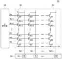
参见图5,示出了示例性存储系统以图示典型的SPOR过程。该存储系统包括DRAM500,DRAM 500包括FTL 510。DRAM 500通常与存储器/NAND 502分离。NAND 502包括多个超级块。为了具有最大的并行度,每个裸片中的具有同一块索引的物理块被分组成超级块。同一超级块的每个物理块中的具有同一页索引的页被分组成超级页。当超级块充满且准备闭合时,超级块中的页的LBA被写入在其最后作为元页(例如,图5中的MP)。当突然断电发生时,NAND 502具有两个开放块(一个用于主机写入的开放块530和一个用于垃圾收集(GC)的开放块540)以及很多其他闭合块(例如,闭合超级块)。Referring to Figure 5, an exemplary storage system is shown to illustrate a typical SPOR process. The memory system includes
在SPOR期间,对于开放块530和540,需要读出所有的用户页,且需要为它们中的每个恢复LBA。对于闭合块,可以读取元页MP,以及按照时间次序(意味着最旧的元页最先)对表FTL更新(或重放)映射信息。这样,对于特定的LBA,有效映射信息将覆盖无效映射信息。当重放/更新完成时,整个表被重建了,且主机命令可以开始起作用。During SPOR, for
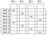
接下来参见图6A和图6B,示出了超级块的示图60和62。超级块可以指一起来分配、写入和擦除的一组块/页,且超级块利用每个芯片/平面/裸片中的一个块来保存元数据。如所示,超级块100包括裸片0的页100、裸片1的页100、裸片2的页100和裸片3的页100。元数据用来描述页中的数据,也可以表示超级块的类型(例如,闭合超级块、主机写入开放超级块、垃圾收集开放超级块等)。Referring next to Figures 6A and 6B, diagrams 60 and 62 of superblocks are shown. A superblock can refer to a group of blocks/pages that are allocated, written, and erased together, and utilizes one block in each chip/plane/die to hold metadata. As shown,
如图6B中所述,对超级块的先前布置和设计意在包括沿同一裸片的元块(例如,用于储存元数据的块或元页等)。例如,超级块100至超级块107中的每个包括他们在裸片3上的对应元块。As described in Figure 6B, the previous arrangement and design of superblocks is intended to include metablocks (eg, blocks or metapages, etc.) along the same die. For example, each of
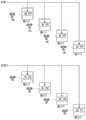
在图7中,示图示出了对诸如图6A和图6B中所示的超级块的超级块配置执行的读取。一旦SPOR过程启动,就执行读取命令以重建LBA表。读取命令用来判断哪些超级块是开放的、哪些超级块是闭合的、超级块闭合的次序等,这通常通过从元块读取元数据或元页来判断。In Figure 7, a diagram shows a read performed on a superblock configuration such as that shown in Figures 6A and 6B. Once the SPOR process starts, a read command is executed to rebuild the LBA table. The read command is used to determine which superblocks are open, which superblocks are closed, the order in which the superblocks are closed, etc. This is usually determined by reading metadata or metapages from metablocks.
在图6A和图6B所示的元块在每个超级块的同一裸片上的示例中,当发送了读取命令时,将访问多个裸片之中的同一页。例如,如果读取命令是针对页100的,则其从裸片0至裸片3中的每个读取页100(例如,图7中的Read1),其中,裸片0至裸片3中的每个的页100包含针对单个超级块(超级块100)的超级块信息。对于SPOR过程,所需的关键信息是包含在元块/元页/元数据中的信息。因此,读取命令将最终读取裸片3处的元块,此外其还将必须读取裸片0、裸片1和裸片2处的非元块,这增加了重建时间,因为对于LBA表重建来说这些读取通常是不必要的。当考虑在所示示例中以类似方式执行8个读取操作(例如,Read1-Read8)时,对LBA表重建执行了24个额外且不必要的读取。In the example shown in FIGS. 6A and 6B where the metablock is on the same die for each superblock, when a read command is sent, the same page among multiple dies is accessed. For example, if the read command is for
因此,这里公开的本发明的示例试图减少突然断电之后完成LBA表重建所必需的读取的数量。Accordingly, the examples of the invention disclosed herein seek to reduce the number of reads necessary to complete the LBA table rebuild after a sudden power outage.
图8是根据本发明若干方面的用于储存元数据以及重建LBA表的步骤的流程图80。图9是根据本发明若干方面的包括元块的超级块布局的示图。图10是根据本发明若干方面的SPOR过程期间执行的示例性读取的示图。8 is a
虽然本文中使用术语元块、元页和元数据来描述本发明,但本领域技术人员将认识到这些术语指用来在SPOR过程期间重建LBA表的信息。该信息可以为元数据的形式,可以储存在元页中,可以位于元块中等。Although the terms metablock, metapage, and metadata are used herein to describe the present invention, those skilled in the art will recognize that these terms refer to the information used to reconstruct the LBA table during the SPOR process. This information can be in the form of metadata, can be stored in a metapage, can be located in a metablock, or the like.
参见图8,在步骤800处,闭合第一超级块,以及产生与第一超级块相对应的第一元页。如上所述,当超级块要闭合时,包括用于SPOR过程的信息的元页或元数据被产生,且其与其所对应的超级块关联地储存。8, at
在步骤802处,将第一元页储存在第一超级块的裸片处。例如,参见图9,当超级块100闭合时,元页(例如,可以储存在元块上)可以储存和位于裸片0处(如示例所示为4NAND配置)。At
在步骤804处,闭合第二超级块,以及产生与第二超级块相对应的第二元页。At
在步骤806处,将第二元页储存在第二超级块的裸片处,使得第二元页的储存位置与第一元页的储存位置错开。例如,参见图9,超级块100的元块储存和位于裸片0处,而超级块101的元块储存和位于裸片1处。超级块100的元块的位置与超级块101的元块的位置错开,意味着它们储存在彼此不同的裸片上。At
如图9中所示,由于此示例描述了4NAND配置,因此多达4个元块的位置可以彼此错开(例如,意味着储存和位于不同的裸片上)。虽然本文中公开的示例示出了4NAND配置,但这是示例性的而非排他性的。NAND配置的其他大小适用于实践本发明,这将改变可以彼此错开的元块的数量。因此,超级块100、101、102和103的元块中的每个彼此错开,且元块104、105、106和107中的每个彼此错开。As shown in Figure 9, since this example describes a 4NAND configuration, the locations of up to 4 metablocks can be staggered from each other (eg, meaning storage and on different dies). Although the examples disclosed herein show a 4NAND configuration, this is exemplary and not exclusive. Other sizes of NAND configurations suitable for practicing the present invention will vary the number of metablocks that can be staggered from each other. Thus, each of the metablocks of
在步骤808处,启动SPOR过程,以及执行读取操作。该读取操作被执行,使得在同一读取操作期间访问第一元页和第二元页。At
如上关于现有技术的存储器配置所讨论的,单个读取将仅访问单个元页。然而,参见图10,在单个读取操作期间,本文中公开的本发明允许单个读取来访问多个元页。在图10中,读取操作Read1可以访问裸片0上的页100、裸片1上的页101、裸片2上的页102和裸片3上的页103(其中,每个页对应于不同的超级块),而不是读取全部4个裸片上的第100页。注意,这些页彼此错开。结果,超级块100、101、102和103可以被配置为使得超级块100的元块被储存在裸片0的页100处、超级块101的元块被储存在裸片1的页101处等(如图9中所示)。因此,读取操作可以在单个读取操作期间访问全部4个超级块(超级块100-103)的元页(例如,用来重建LBA表所必需的信息,诸如判断超级块是开放的还是闭合的),导致读取减少四倍。As discussed above with respect to prior art memory configurations, a single read will only access a single metapage. However, referring to Figure 10, the invention disclosed herein allows a single read to access multiple metapages during a single read operation. In Figure 10, a read operation Read1 may access
这种系统将通过减少如在SPOR中所进行的读取多个超级块所需的时间来改善存储器件(例如,SSD)的性能。Such a system would improve the performance of storage devices (eg, SSDs) by reducing the time required to read multiple superblocks as done in SPOR.
虽然已经为了清楚理解的目的而相当详细地描述了前述实施例,但本发明不局限于所提供的细节。存在很多实施本发明的替代方法。所公开的实施例是说明性的而非限制性的。Although the foregoing embodiments have been described in considerable detail for purposes of clarity of understanding, the invention is not limited to the details provided. There are many alternative ways of implementing the present invention. The disclosed embodiments are illustrative and not restrictive.
Claims (16)
Applications Claiming Priority (3)
| Application Number | Priority Date | Filing Date | Title |
|---|---|---|---|
| US201562138278P | 2015-03-25 | 2015-03-25 | |
| US15/081,644US10180805B2 (en) | 2015-03-25 | 2016-03-25 | Memory system and operating method thereof |
| US15/081,644 | 2016-03-25 |
Publications (2)
| Publication Number | Publication Date |
|---|---|
| CN107229577A CN107229577A (en) | 2017-10-03 |
| CN107229577Btrue CN107229577B (en) | 2020-12-25 |
Family
ID=56974148
Family Applications (1)
| Application Number | Title | Priority Date | Filing Date |
|---|---|---|---|
| CN201610269575.2AActiveCN107229577B (en) | 2015-03-25 | 2016-04-27 | Storage system and operation method thereof |
Country Status (2)
| Country | Link |
|---|---|
| US (1) | US10180805B2 (en) |
| CN (1) | CN107229577B (en) |
Families Citing this family (20)
| Publication number | Priority date | Publication date | Assignee | Title |
|---|---|---|---|---|
| US10540274B2 (en)* | 2016-03-29 | 2020-01-21 | Micron Technology, Inc. | Memory devices including dynamic superblocks, and related methods and electronic systems |
| KR102769764B1 (en)* | 2016-10-14 | 2025-02-20 | 에스케이하이닉스 주식회사 | Controller, memory system and operating method thereof |
| TWI613652B (en)* | 2017-03-27 | 2018-02-01 | 慧榮科技股份有限公司 | Data storage device and operating method therefor |
| TWI646554B (en)* | 2017-03-28 | 2019-01-01 | 慧榮科技股份有限公司 | Data storage device and operating method therefor |
| KR102234725B1 (en)* | 2017-05-30 | 2021-04-02 | 에스케이하이닉스 주식회사 | Controller and memory system and operating method of memory system |
| US10802727B2 (en)* | 2017-06-07 | 2020-10-13 | ScaleFlux, Inc. | Solid-state storage power failure protection using distributed metadata checkpointing |
| US10446197B2 (en) | 2017-08-31 | 2019-10-15 | Micron Technology, Inc. | Optimized scan interval |
| JP7074453B2 (en)* | 2017-10-30 | 2022-05-24 | キオクシア株式会社 | Memory system and control method |
| US10445230B2 (en) | 2017-12-08 | 2019-10-15 | Macronix International Co., Ltd. | Managing block arrangement of super blocks |
| US10387243B2 (en) | 2017-12-08 | 2019-08-20 | Macronix International Co., Ltd. | Managing data arrangement in a super block |
| KR102492729B1 (en)* | 2017-12-13 | 2023-01-27 | 마이크론 테크놀로지, 인크. | Variable width superblock addressing |
| KR102504765B1 (en)* | 2017-12-22 | 2023-03-03 | 에스케이하이닉스 주식회사 | Memory system and operating method thereof |
| US10949113B2 (en)* | 2018-01-10 | 2021-03-16 | SK Hynix Inc. | Retention aware block mapping in flash-based solid state drives |
| US10365854B1 (en)* | 2018-03-19 | 2019-07-30 | Micron Technology, Inc. | Tracking data temperatures of logical block addresses |
| KR102559528B1 (en)* | 2018-03-20 | 2023-07-26 | 에스케이하이닉스 주식회사 | Memory system and operation method thereof |
| TWI687811B (en)* | 2018-05-14 | 2020-03-11 | 慧榮科技股份有限公司 | Data storage apparatus and system information programming mehtod |
| CN110489051A (en)* | 2018-05-14 | 2019-11-22 | 慧荣科技股份有限公司 | The programmed method of data memory device and system information |
| KR102583810B1 (en)* | 2018-05-15 | 2023-10-05 | 에스케이하이닉스 주식회사 | Memory system and operation method thereof |
| KR102787268B1 (en)* | 2019-05-15 | 2025-03-26 | 에스케이하이닉스 주식회사 | Memory system, memory controller and memory device |
| US11809748B2 (en)* | 2022-03-10 | 2023-11-07 | Silicon Motion, Inc. | Control method of flash memory controller and associated flash memory controller and electronic device |
Citations (4)
| Publication number | Priority date | Publication date | Assignee | Title |
|---|---|---|---|---|
| US20070086260A1 (en)* | 2005-10-13 | 2007-04-19 | Sinclair Alan W | Method of storing transformed units of data in a memory system having fixed sized storage blocks |
| US20110302365A1 (en)* | 2009-02-13 | 2011-12-08 | Indilinx Co., Ltd. | Storage system using a rapid storage device as a cache |
| CN102314321A (en)* | 2010-07-07 | 2012-01-11 | 深圳市朗科科技股份有限公司 | Storage system and method and device for accessing data by using same |
| CN103150275A (en)* | 2007-12-27 | 2013-06-12 | 桑迪士克企业知识产权有限责任公司 | Flash memory controller having reduced pinout |
Family Cites Families (3)
| Publication number | Priority date | Publication date | Assignee | Title |
|---|---|---|---|---|
| US9164686B2 (en)* | 2007-06-29 | 2015-10-20 | Seagate Technology, Llc | Virtual storage space with cyclical wrapping grid function |
| US9645763B2 (en) | 2014-01-13 | 2017-05-09 | Seagate Technology Llc | Framework for balancing robustness and latency during collection of statistics from soft reads |
| US9823863B1 (en)* | 2014-06-30 | 2017-11-21 | Sk Hynix Memory Solutions Inc. | Sub-blocks and meta pages for mapping table rebuild |
- 2016
- 2016-03-25USUS15/081,644patent/US10180805B2/enactiveActive
- 2016-04-27CNCN201610269575.2Apatent/CN107229577B/enactiveActive
Patent Citations (4)
| Publication number | Priority date | Publication date | Assignee | Title |
|---|---|---|---|---|
| US20070086260A1 (en)* | 2005-10-13 | 2007-04-19 | Sinclair Alan W | Method of storing transformed units of data in a memory system having fixed sized storage blocks |
| CN103150275A (en)* | 2007-12-27 | 2013-06-12 | 桑迪士克企业知识产权有限责任公司 | Flash memory controller having reduced pinout |
| US20110302365A1 (en)* | 2009-02-13 | 2011-12-08 | Indilinx Co., Ltd. | Storage system using a rapid storage device as a cache |
| CN102314321A (en)* | 2010-07-07 | 2012-01-11 | 深圳市朗科科技股份有限公司 | Storage system and method and device for accessing data by using same |
Also Published As
| Publication number | Publication date |
|---|---|
| US10180805B2 (en) | 2019-01-15 |
| US20160283138A1 (en) | 2016-09-29 |
| CN107229577A (en) | 2017-10-03 |
Similar Documents
| Publication | Publication Date | Title |
|---|---|---|
| CN107229577B (en) | Storage system and operation method thereof | |
| CN107239228B (en) | Memory system and method of operation to improve rebuild efficiency | |
| US10460774B2 (en) | Apparatus and method capable of removing duplication write of data in memory | |
| US10318414B2 (en) | Memory system and memory management method thereof | |
| CN106095699B (en) | Scalable SPOR Algorithm for Flash Memory | |
| US10296452B2 (en) | Data separation by delaying hot block garbage collection | |
| CN108108308B (en) | Memory system and method of operation | |
| CN109032501B (en) | Memory system and operating method thereof | |
| CN106372004B (en) | Programmable protocol independent BAR memory for SSD controller | |
| CN107957959B (en) | Memory system with file-level secure erase and method of operation | |
| CN106372011B (en) | High-performance host queue monitor for PCIE SSD controllers | |
| CN109800178B (en) | Garbage collection method and memory system for hybrid address mapping | |
| US9946644B2 (en) | Memory system and operating method thereof | |
| US20160334999A1 (en) | Reduction of maximum latency using dynamic self-tuning for redundant array of independent disks | |
| CN110825316A (en) | Controller and operation method of the controller | |
| KR20180008966A (en) | Memory system and operating method of memory system | |
| CN112216328B (en) | Memory system with low complexity decoding and method of operation thereof | |
| CN110275844A (en) | Memory system and method of operation using adaptive threshold decoding | |
| CN110047554B (en) | Memory system with superchip deletion recovery and method of operation thereof | |
| CN109947661B (en) | Memory system and method of operating the same | |
| US10141072B2 (en) | Efficient encoder based on modified RU algorithm | |
| US11520507B1 (en) | System and method for test precondition generation based on factory-formatted state of memory device | |
| CN110069428B (en) | System data compression and reconstruction method and system | |
| CN110058798B (en) | Data processing system and method of operation | |
| CN108073469B (en) | Data Mapping Scheme for Universal Product Codes |
Legal Events
| Date | Code | Title | Description |
|---|---|---|---|
| PB01 | Publication | ||
| PB01 | Publication | ||
| SE01 | Entry into force of request for substantive examination | ||
| SE01 | Entry into force of request for substantive examination | ||
| GR01 | Patent grant | ||
| GR01 | Patent grant |