CN107112394B - Light emitting diode and light emitting diode array comprising the same - Google Patents
Light emitting diode and light emitting diode array comprising the sameDownload PDFInfo
- Publication number
- CN107112394B CN107112394BCN201580071060.5ACN201580071060ACN107112394BCN 107112394 BCN107112394 BCN 107112394BCN 201580071060 ACN201580071060 ACN 201580071060ACN 107112394 BCN107112394 BCN 107112394B
- Authority
- CN
- China
- Prior art keywords
- light emitting
- conductive semiconductor
- layer
- electrode
- semiconductor layer
- Prior art date
- Legal status (The legal status is an assumption and is not a legal conclusion. Google has not performed a legal analysis and makes no representation as to the accuracy of the status listed.)
- Active
Links
Images


Classifications
- H—ELECTRICITY
- H10—SEMICONDUCTOR DEVICES; ELECTRIC SOLID-STATE DEVICES NOT OTHERWISE PROVIDED FOR
- H10H—INORGANIC LIGHT-EMITTING SEMICONDUCTOR DEVICES HAVING POTENTIAL BARRIERS
- H10H20/00—Individual inorganic light-emitting semiconductor devices having potential barriers, e.g. light-emitting diodes [LED]
- H10H20/80—Constructional details
- H10H20/81—Bodies
- H10H20/814—Bodies having reflecting means, e.g. semiconductor Bragg reflectors
- H—ELECTRICITY
- H10—SEMICONDUCTOR DEVICES; ELECTRIC SOLID-STATE DEVICES NOT OTHERWISE PROVIDED FOR
- H10H—INORGANIC LIGHT-EMITTING SEMICONDUCTOR DEVICES HAVING POTENTIAL BARRIERS
- H10H20/00—Individual inorganic light-emitting semiconductor devices having potential barriers, e.g. light-emitting diodes [LED]
- H10H20/80—Constructional details
- H10H20/84—Coatings, e.g. passivation layers or antireflective coatings
- H10H20/841—Reflective coatings, e.g. dielectric Bragg reflectors
- H—ELECTRICITY
- H01—ELECTRIC ELEMENTS
- H01L—SEMICONDUCTOR DEVICES NOT COVERED BY CLASS H10
- H01L25/00—Assemblies consisting of a plurality of semiconductor or other solid state devices
- H01L25/03—Assemblies consisting of a plurality of semiconductor or other solid state devices all the devices being of a type provided for in a single subclass of subclasses H10B, H10D, H10F, H10H, H10K or H10N, e.g. assemblies of rectifier diodes
- H01L25/04—Assemblies consisting of a plurality of semiconductor or other solid state devices all the devices being of a type provided for in a single subclass of subclasses H10B, H10D, H10F, H10H, H10K or H10N, e.g. assemblies of rectifier diodes the devices not having separate containers
- H01L25/075—Assemblies consisting of a plurality of semiconductor or other solid state devices all the devices being of a type provided for in a single subclass of subclasses H10B, H10D, H10F, H10H, H10K or H10N, e.g. assemblies of rectifier diodes the devices not having separate containers the devices being of a type provided for in group H10H20/00
- H01L25/0753—Assemblies consisting of a plurality of semiconductor or other solid state devices all the devices being of a type provided for in a single subclass of subclasses H10B, H10D, H10F, H10H, H10K or H10N, e.g. assemblies of rectifier diodes the devices not having separate containers the devices being of a type provided for in group H10H20/00 the devices being arranged next to each other
- H—ELECTRICITY
- H10—SEMICONDUCTOR DEVICES; ELECTRIC SOLID-STATE DEVICES NOT OTHERWISE PROVIDED FOR
- H10H—INORGANIC LIGHT-EMITTING SEMICONDUCTOR DEVICES HAVING POTENTIAL BARRIERS
- H10H20/00—Individual inorganic light-emitting semiconductor devices having potential barriers, e.g. light-emitting diodes [LED]
- H10H20/01—Manufacture or treatment
- H10H20/011—Manufacture or treatment of bodies, e.g. forming semiconductor layers
- H10H20/018—Bonding of wafers
- H—ELECTRICITY
- H10—SEMICONDUCTOR DEVICES; ELECTRIC SOLID-STATE DEVICES NOT OTHERWISE PROVIDED FOR
- H10H—INORGANIC LIGHT-EMITTING SEMICONDUCTOR DEVICES HAVING POTENTIAL BARRIERS
- H10H20/00—Individual inorganic light-emitting semiconductor devices having potential barriers, e.g. light-emitting diodes [LED]
- H10H20/80—Constructional details
- H10H20/81—Bodies
- H10H20/814—Bodies having reflecting means, e.g. semiconductor Bragg reflectors
- H10H20/8142—Bodies having reflecting means, e.g. semiconductor Bragg reflectors forming resonant cavity structures
- H—ELECTRICITY
- H10—SEMICONDUCTOR DEVICES; ELECTRIC SOLID-STATE DEVICES NOT OTHERWISE PROVIDED FOR
- H10H—INORGANIC LIGHT-EMITTING SEMICONDUCTOR DEVICES HAVING POTENTIAL BARRIERS
- H10H20/00—Individual inorganic light-emitting semiconductor devices having potential barriers, e.g. light-emitting diodes [LED]
- H10H20/80—Constructional details
- H10H20/81—Bodies
- H10H20/819—Bodies characterised by their shape, e.g. curved or truncated substrates
- H—ELECTRICITY
- H10—SEMICONDUCTOR DEVICES; ELECTRIC SOLID-STATE DEVICES NOT OTHERWISE PROVIDED FOR
- H10H—INORGANIC LIGHT-EMITTING SEMICONDUCTOR DEVICES HAVING POTENTIAL BARRIERS
- H10H20/00—Individual inorganic light-emitting semiconductor devices having potential barriers, e.g. light-emitting diodes [LED]
- H10H20/80—Constructional details
- H10H20/83—Electrodes
- H10H20/831—Electrodes characterised by their shape
- H10H20/8314—Electrodes characterised by their shape extending at least partially onto an outer side surface of the bodies
- H—ELECTRICITY
- H10—SEMICONDUCTOR DEVICES; ELECTRIC SOLID-STATE DEVICES NOT OTHERWISE PROVIDED FOR
- H10H—INORGANIC LIGHT-EMITTING SEMICONDUCTOR DEVICES HAVING POTENTIAL BARRIERS
- H10H20/00—Individual inorganic light-emitting semiconductor devices having potential barriers, e.g. light-emitting diodes [LED]
- H10H20/80—Constructional details
- H10H20/83—Electrodes
- H10H20/832—Electrodes characterised by their material
- H10H20/835—Reflective materials
- H—ELECTRICITY
- H10—SEMICONDUCTOR DEVICES; ELECTRIC SOLID-STATE DEVICES NOT OTHERWISE PROVIDED FOR
- H10H—INORGANIC LIGHT-EMITTING SEMICONDUCTOR DEVICES HAVING POTENTIAL BARRIERS
- H10H20/00—Individual inorganic light-emitting semiconductor devices having potential barriers, e.g. light-emitting diodes [LED]
- H10H20/80—Constructional details
- H10H20/85—Packages
- H10H20/857—Interconnections, e.g. lead-frames, bond wires or solder balls
- H—ELECTRICITY
- H10—SEMICONDUCTOR DEVICES; ELECTRIC SOLID-STATE DEVICES NOT OTHERWISE PROVIDED FOR
- H10H—INORGANIC LIGHT-EMITTING SEMICONDUCTOR DEVICES HAVING POTENTIAL BARRIERS
- H10H20/00—Individual inorganic light-emitting semiconductor devices having potential barriers, e.g. light-emitting diodes [LED]
- H10H20/01—Manufacture or treatment
- H10H20/032—Manufacture or treatment of electrodes
- H—ELECTRICITY
- H10—SEMICONDUCTOR DEVICES; ELECTRIC SOLID-STATE DEVICES NOT OTHERWISE PROVIDED FOR
- H10H—INORGANIC LIGHT-EMITTING SEMICONDUCTOR DEVICES HAVING POTENTIAL BARRIERS
- H10H20/00—Individual inorganic light-emitting semiconductor devices having potential barriers, e.g. light-emitting diodes [LED]
- H10H20/01—Manufacture or treatment
- H10H20/034—Manufacture or treatment of coatings
- H—ELECTRICITY
- H10—SEMICONDUCTOR DEVICES; ELECTRIC SOLID-STATE DEVICES NOT OTHERWISE PROVIDED FOR
- H10H—INORGANIC LIGHT-EMITTING SEMICONDUCTOR DEVICES HAVING POTENTIAL BARRIERS
- H10H20/00—Individual inorganic light-emitting semiconductor devices having potential barriers, e.g. light-emitting diodes [LED]
- H10H20/01—Manufacture or treatment
- H10H20/036—Manufacture or treatment of packages
- H10H20/0364—Manufacture or treatment of packages of interconnections
- Y—GENERAL TAGGING OF NEW TECHNOLOGICAL DEVELOPMENTS; GENERAL TAGGING OF CROSS-SECTIONAL TECHNOLOGIES SPANNING OVER SEVERAL SECTIONS OF THE IPC; TECHNICAL SUBJECTS COVERED BY FORMER USPC CROSS-REFERENCE ART COLLECTIONS [XRACs] AND DIGESTS
- Y10—TECHNICAL SUBJECTS COVERED BY FORMER USPC
- Y10S—TECHNICAL SUBJECTS COVERED BY FORMER USPC CROSS-REFERENCE ART COLLECTIONS [XRACs] AND DIGESTS
- Y10S362/00—Illumination
- Y10S362/80—Light emitting diode
Landscapes
- Engineering & Computer Science (AREA)
- Power Engineering (AREA)
- Microelectronics & Electronic Packaging (AREA)
- Physics & Mathematics (AREA)
- Condensed Matter Physics & Semiconductors (AREA)
- General Physics & Mathematics (AREA)
- Computer Hardware Design (AREA)
- Led Devices (AREA)
- Led Device Packages (AREA)
Abstract
Description
Translated fromChinese技术领域technical field
实施例涉及一种发光二极管和包括该发光二极管的发光二极管阵列。Embodiments relate to a light emitting diode and a light emitting diode array including the same.
背景技术Background technique
诸如GaN和AlGaN等第III-V族化合物半导体由于其许多优点(例如,宽且容易调节的带隙能量)而广泛用于光电子学以及电子设备。Group III-V compound semiconductors such as GaN and AlGaN are widely used in optoelectronics as well as electronic devices due to their many advantages (eg, wide and easily tunable bandgap energy).
特别地,使用第III-V族或第II-VI族化合物半导体材料的发光器件(诸如发光二极管和激光二极管)能够凭借薄膜生长技术和器件材料的发展呈现诸如红色、绿色、蓝色和紫外等各种颜色,能够使用荧光材料或通过混色产生高效率的白光,并且与诸如荧光灯和白炽灯等常规光源相比,具有诸如低功耗、半永久寿命、快速响应速度、安全以及环保等优点。In particular, light-emitting devices (such as light-emitting diodes and laser diodes) using Group III-V or Group II-VI compound semiconductor materials can exhibit colors such as red, green, blue, and ultraviolet due to the development of thin film growth technology and device materials. Various colors can be produced using fluorescent materials or through color mixing to generate high-efficiency white light, and compared with conventional light sources such as fluorescent lamps and incandescent lamps, it has advantages such as low power consumption, semi-permanent life, fast response speed, safety, and environmental protection.
因此,这样的发光器件越来越多地应用于光通信单元的发送模块、作为构成液晶显示(LCD)器件背光的冷阴极荧光灯(CCFL)的替代的发光二极管背光、使用白色发光二极管作为荧光灯或白炽灯的替代的照明装置、车前灯、以及红绿灯。Therefore, such light-emitting devices are increasingly applied to transmission modules of optical communication units, light-emitting diode backlights as an alternative to cold cathode fluorescent lamps (CCFLs) constituting the backlights of liquid crystal display (LCD) devices, use of white light-emitting diodes as fluorescent lamps or Alternative lighting devices for incandescent lamps, headlights, and traffic lights.
在传统的发光器件中,形成包括n型半导体层、有源层和p型半导体层的发光结构,并且当经由n型半导体层注入有源层的电子与经由p型半导体层注入有源层的空穴结合时,传统发光器件发射的光具有的能量是由有源层的材料的本征能带决定的。In a conventional light-emitting device, a light-emitting structure including an n-type semiconductor layer, an active layer, and a p-type semiconductor layer is formed, and when electrons injected into the active layer via the n-type semiconductor layer and electrons injected into the active layer via the p-type semiconductor layer When holes are combined, the energy of light emitted by a conventional light-emitting device is determined by the intrinsic energy band of the material of the active layer.
已经作出了形成像素同时减小发光结构的横截面积的许多尝试,但是因为每个发光结构的厚度太大,所以难以实现超薄单位像素。Many attempts have been made to form pixels while reducing the cross-sectional area of light emitting structures, but it is difficult to realize ultrathin unit pixels because the thickness of each light emitting structure is too large.
也就是说,上述发光结构生长在由蓝宝石等形成的衬底上,然而,在生长发光结构之后将衬底保持原样的水平型发光二极管中,或者在将金属支撑件耦合到发光结构的一部分之后去除衬底的垂直型发光二极管中,因为衬底或金属支撑件具有的厚度大,所以难以实现超薄像素。That is, the above-mentioned light emitting structure is grown on a substrate formed of sapphire or the like, however, in a horizontal type light emitting diode in which the substrate is left as it is after growing the light emitting structure, or after a metal support is coupled to a part of the light emitting structure In the vertical type light emitting diode in which the substrate is removed, since the substrate or the metal support has a large thickness, it is difficult to realize an ultra-thin pixel.
发明内容SUMMARY OF THE INVENTION
【技术问题】【technical problem】
实施例提供一种省略了生长衬底或金属支撑件的超薄发光二极管。Embodiments provide an ultra-thin light emitting diode that omits a growth substrate or metal support.
【技术方案】【Technical solutions】
在一个实施例中,一种发光二极管包括:发光结构,包括:第一导电半导体层;有源层,布置在第一导电半导体层上;以及第二导电半导体层,布置在有源层上;第一电极,布置在第一导电半导体层的一部分上;绝缘层,布置在第一电极、第一导电半导体层、有源层、以及第二导电半导体层的一部分上,绝缘层具有DBR结构;以及第二电极,布置在第二导电半导体层上,其中第一电极包括第一表面和第二表面,第一表面与布置在第一电极上的绝缘层接触,第二表面与第一表面相对并被暴露。In one embodiment, a light emitting diode includes: a light emitting structure including: a first conductive semiconductor layer; an active layer disposed on the first conductive semiconductor layer; and a second conductive semiconductor layer disposed on the active layer; The first electrode is arranged on a part of the first conductive semiconductor layer; the insulating layer is arranged on the first electrode, the first conductive semiconductor layer, the active layer, and a part of the second conductive semiconductor layer, and the insulating layer has a DBR structure; and a second electrode disposed on the second conductive semiconductor layer, wherein the first electrode includes a first surface and a second surface, the first surface is in contact with the insulating layer disposed on the first electrode, and the second surface is opposite the first surface and exposed.
发光结构可以包括第一台面(mesa)区域,第一导电半导体层可以包括第二台面区域,并且第一电极可以布置在第二台面区域中的第一导电半导体层上。The light emitting structure may include a first mesa region, the first conductive semiconductor layer may include a second mesa region, and the first electrode may be disposed on the first conductive semiconductor layer in the second mesa region.
第一电极可以布置在第二台面区域中的第一导电半导体层的侧表面上。The first electrode may be arranged on a side surface of the first conductive semiconductor layer in the second mesa region.
第一电极可以延伸到第二台面区域的周边。The first electrode may extend to the periphery of the second mesa region.
使第二导电半导体层暴露的开放(open)区域可以布置在第一台面区域上,并且第二电极的至少一部分可以布置在开放区域上。An open area exposing the second conductive semiconductor layer may be disposed on the first mesa area, and at least a portion of the second electrode may be disposed on the open area.
第二导电半导体层、绝缘层和第二电极的至少一部分在第一台面蚀刻区域的开放区域的周边彼此重叠。At least a portion of the second conductive semiconductor layer, the insulating layer, and the second electrode overlap each other at the periphery of the open region of the first mesa-etched region.
DBR结构可以形成为使得TiO2和SiO2的配置或Ta2O5和SiO2的配置重复至少两次。The DBR structure may be formed such that the configuration of TiO2 and SiO2 or the configuration of Ta2 O5 and SiO2 is repeated at least twice.
第一电极可以包括欧姆层、反射层、以及布置在反射层上的耦合层。The first electrode may include an ohmic layer, a reflective layer, and a coupling layer disposed on the reflective layer.
耦合层可以包括钛(Ti)。The coupling layer may include titanium (Ti).
第二电极可以包括欧姆层和反射层。The second electrode may include an ohmic layer and a reflective layer.
第二电极的欧姆层可以包括铬(Cr)、银(Ag)或钛(Ti)。The ohmic layer of the second electrode may include chromium (Cr), silver (Ag), or titanium (Ti).
第二电极的欧姆层可以具有1nm或更小的厚度。The ohmic layer of the second electrode may have a thickness of 1 nm or less.
反射层可以包括:铂(Pt)和金(Au)的合金,镍(Ni)和金(Au)的合金,铝(Al)、铂(Au)和金(Au)的合金,或铝(Al)、镍(Ni)和金(Au)的合金。The reflective layer may include: an alloy of platinum (Pt) and gold (Au), an alloy of nickel (Ni) and gold (Au), an alloy of aluminum (Al), platinum (Au) and gold (Au), or an alloy of aluminum (Al) ), an alloy of nickel (Ni) and gold (Au).
在另一个实施例中,一种发光二极管阵列包括电路板和多个发光二极管,每个发光二极管包括:发光结构,布置在电路板上且包括:第一导电半导体层;有源层,布置在第一导电半导体层上;以及第二导电半导体层,布置在有源层上;第一电极,布置在第一导电半导体层的一部分上;绝缘层,布置在第一电极、第一导电半导体层、有源层、以及第二导电半导体层的一部分上,绝缘层具有DBR结构;以及第二电极,布置在第二导电半导体层上,其中第一电极包括第一表面和第二表面,第一表面与布置在第一电极上的绝缘层接触,第二表面与第一表面相对并被暴露;以及各向异性导电膜(ACF),布置在电路板与发光二极管之间,其中ACF包括:基材;以及多个导电球,设置在基材中,并且导电球与电路板和第二电极接触。In another embodiment, a light emitting diode array includes a circuit board and a plurality of light emitting diodes, each light emitting diode including: a light emitting structure arranged on the circuit board and comprising: a first conductive semiconductor layer; an active layer arranged on the on the first conductive semiconductor layer; and a second conductive semiconductor layer, arranged on the active layer; a first electrode, arranged on a part of the first conductive semiconductor layer; an insulating layer, arranged on the first electrode, the first conductive semiconductor layer , the active layer, and a part of the second conductive semiconductor layer, the insulating layer has a DBR structure; and a second electrode, arranged on the second conductive semiconductor layer, wherein the first electrode includes a first surface and a second surface, the first a surface is in contact with an insulating layer disposed on the first electrode, the second surface is opposite to the first surface and is exposed; and an anisotropic conductive film (ACF) disposed between the circuit board and the light emitting diode, wherein the ACF includes: a base material; and a plurality of conductive balls disposed in the base material, and the conductive balls are in contact with the circuit board and the second electrode.
绝缘层可以布置在第一电极的第一表面、第一导电半导体层、有源层、以及第二导电半导体层的一部分上。An insulating layer may be disposed on the first surface of the first electrode, the first conductive semiconductor layer, the active layer, and a portion of the second conductive semiconductor layer.
第一电极的第二表面可以与第二台面区域中的第一导电半导体层的上表面和侧表面接触。The second surface of the first electrode may be in contact with upper and side surfaces of the first conductive semiconductor layer in the second mesa region.
在再一个实施例中,一种发光二极管阵列包括电路板和多个发光二极管,每个发光二极管包括:发光结构,布置在电路板上且包括:第一导电半导体层;有源层,布置在第一导电半导体层上;以及第二导电半导体层,布置在有源层上;第一电极,布置在第一导电半导体层的一部分上;绝缘层,布置在第一电极、第一导电半导体层、有源层、以及第二导电半导体层的一部分上,绝缘层具有DBR结构;及第二电极,布置在第二导电半导体层上,其中第一电极包括第一表面和第二表面,第一表面与布置在第一电极上的绝缘层接触,第二表面与第一表面相对并被暴露;以及各向异性导电膜(ACF),布置在电路板与发光二极管之间,其中ACF包括:基材;以及多个导电球,设置在基材中,并且导电球与电路板和第二电极接触。In yet another embodiment, a light emitting diode array includes a circuit board and a plurality of light emitting diodes, each light emitting diode including: a light emitting structure arranged on the circuit board and comprising: a first conductive semiconductor layer; an active layer arranged on the on the first conductive semiconductor layer; and a second conductive semiconductor layer, arranged on the active layer; a first electrode, arranged on a part of the first conductive semiconductor layer; an insulating layer, arranged on the first electrode, the first conductive semiconductor layer , the active layer, and a part of the second conductive semiconductor layer, the insulating layer has a DBR structure; and a second electrode, arranged on the second conductive semiconductor layer, wherein the first electrode includes a first surface and a second surface, the first a surface is in contact with an insulating layer disposed on the first electrode, the second surface is opposite to the first surface and is exposed; and an anisotropic conductive film (ACF) disposed between the circuit board and the light emitting diode, wherein the ACF includes: a base material; and a plurality of conductive balls disposed in the base material, and the conductive balls are in contact with the circuit board and the second electrode.
每个发光二极管的第一电极可以在与电路板相对定向的区域中使用单个布线结构连接到其他发光二极管的第一电极。The first electrode of each light emitting diode may be connected to the first electrodes of other light emitting diodes using a single wiring structure in an area oriented opposite the circuit board.
【有益效果】【Beneficial effects】
根据实施例的发光二极管和包括该发光二极管的发光二极管阵列,具有DBR结构的绝缘层布置在发光结构的上表面、第二电极的上表面的一部分以及第一电极的上表面上,由此,从有源层发射的光可以被反射到发光二极管的下表面。According to the light emitting diode and the light emitting diode array including the light emitting diode of the embodiment, the insulating layer having the DBR structure is arranged on the upper surface of the light emitting structure, a part of the upper surface of the second electrode, and the upper surface of the first electrode, whereby, Light emitted from the active layer may be reflected to the lower surface of the light emitting diode.
此外,除了第一电极和第二电极之外,通过具有DBR结构的绝缘层的反射,可以提高发光效率。In addition, the luminous efficiency can be improved by the reflection of the insulating layer having the DBR structure in addition to the first electrode and the second electrode.
而且,在形成第二电极的过程中,可以通过将第二电极形成得比透射导电层的开放区域宽,来防止光泄漏。Also, in the process of forming the second electrode, light leakage can be prevented by forming the second electrode wider than the open area of the transmissive conductive layer.
附图说明Description of drawings
图1是发光二极管的实施例的截面图;1 is a cross-sectional view of an embodiment of a light emitting diode;
图2是示出第一电极的结构的详细视图;FIG. 2 is a detailed view showing the structure of the first electrode;
图3是示出第二电极的结构的详细视图;3 is a detailed view showing the structure of the second electrode;
图4是示出钝化层的结构的详细视图;4 is a detailed view showing the structure of the passivation layer;
图5a至图5j是示出发光二极管的制造工艺的视图;5a to 5j are views illustrating a manufacturing process of the light emitting diode;
图6是图1所示的发光二极管的俯视图;FIG. 6 is a top view of the light-emitting diode shown in FIG. 1;
图7a和图7b是图1所示的发光二极管的立体图和侧视图;以及Figures 7a and 7b are perspective and side views of the light emitting diode shown in Figure 1; and
图8是示出包括发光二极管阵列的智能手表的实施例的视图。FIG. 8 is a view illustrating an embodiment of a smart watch including a light emitting diode array.
具体实施方式Detailed ways
下文将参考附图详细描述实施例。Hereinafter, the embodiments will be described in detail with reference to the accompanying drawings.
应当理解,当一个元件被称为位于另一个元件“上”或“下”时,其可以直接位于该元件上/下,或者也可以存在一个或多个介于中间的元件。当一个元件被称为位于“上”或“下”时,基于该元件,可以包括“位于该元件下”以及“位于该元件上”。It will be understood that when an element is referred to as being "on" or "under" another element, it can be directly on/under the element, or one or more intervening elements may also be present. When an element is referred to as being "on" or "under", "under the element" as well as "on the element" can be included based on the element.
图1是发光二极管的一个实施例的截面图。1 is a cross-sectional view of one embodiment of a light emitting diode.
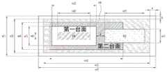
根据该实施例的发光二极管100包括:发光结构120,该发光结构包括第一导电半导体层122、有源层124以及第二导电半导体层126;透射导电层130,布置在第二导电半导体层126上;第一电极142,布置在第一导电半导体层122上;第二电极146,布置在第二导电半导体层126上;以及绝缘层150。The
发光结构120包括第一台面区域和第二台面区域,其中第一台面区域可以布置在第一导电半导体层122、有源层124和第二导电半导体层126上,第二台面区域可以仅布置在第一导电半导体层122上。这是因为第一台面区域在暴露第一导电半导体层122的上表面以形成布置第一电极142的区域的第一蚀刻工艺中形成,第二台面区域在蚀刻所暴露的第一导电半导体层122的边缘以增大布置第一电极142的区域的第二蚀刻工艺中形成,这将在后文进行描述。The
虽然图1示出了第一台面区域和第二台面区域的侧表面大致垂直定向,但是实际上它们也可以倾斜预定角度。Although FIG. 1 shows that the side surfaces of the first mesa region and the second mesa region are oriented substantially vertically, in practice they may also be inclined at a predetermined angle.
第一导电半导体层122可以由第III-V族或第II-VI族化合物半导体制成,并且可以掺杂有第一导电掺杂剂。第一导电半导体层122可以包括分子式为AlxInyGa(1-x-y)N(0≤x≤1,0≤y≤1,以及0≤x+y≤1)的半导体材料,并且可以由例如AlGaN、GaN、InAlGaN、AlGaAs、GaP、GaAs、GaAsP和AlGaInP中的至少之一制成。The first
当第一导电半导体层122是n型半导体层时,第一导电掺杂剂可以包括诸如Si、Ge、Sn、Se或Te等n型掺杂剂。第一导电半导体层122可以形成为具有单层结构或多层结构,但本公开不限于此。When the first
在第一导电半导体层122中,第二台面区域形成在第一台面区域的一侧(图1中的右侧),并且在第二台面区域的右侧形成高度差。In the first
有源层124布置在第一台面区域上的第一导电半导体层122的上表面上,并且可以包括单阱结构、多阱结构、单量子阱结构、多量子阱(MQW)结构、量子点结构以及量子线结构中的一种。The
有源层124可以具有使用第III-V族元素的化合物半导体材料的阱层和阻挡层,例如,可以具有由AlGaN/AlGaN、InGaN/GaN、InGaN/InGaN、AlGaN/GaN、InAlGaN/GaN、GaAs(InGaAs)/AlGaAs和GaP(InGaP)/AlGaP中的至少之一制成的对结构,但本公开不限于此。阱层可以由能带隙比阻挡层的能带隙低的材料制成。The
第二导电半导体层126可以使用半导体化合物形成在有源层124的表面上。第二导电半导体层126可以由第III-V族或第II-VI族化合物半导体制成,并且可以掺杂有第二导电掺杂剂。第二导电半导体层126可以由分子式例如为InxAlyGa1-x-yN(0≤x≤1,0≤y≤1,0≤x+y≤1)的半导体材料制成,并且可以由AlGaN、GaN、AlInN、AlGaAs、GaP、GaAs、GaAsP和AlGaInP中的至少之一制成。The second
第二导电半导体层126可以掺杂有第二导电掺杂剂,并且当第二导电半导体层126是p型半导体层时,第二导电掺杂剂可以是诸如Mg、Zn、Ca、Sr或Ba等p型掺杂剂。第二导电半导体层126可以形成为具有单层结构或多层结构,但是本公开不限于此。The second
由氧化铟锡(ITO)制成的透射导电层130形成在第二导电半导体层126上,从而促进电流从第二电极146传到第二导电半导体层126。A transmissive
第二导电半导体层126、有源层124和第一导电半导体层122被台面蚀刻,使得蚀刻从第二导电半导体层126进行到第一导电半导体层122的一部分,从而暴露第一导电半导体层122以确保形成第一电极146的区域。The second
第一电极142和第二电极146可以分别布置在第一导电半导体层122和第二导电半导体层126上。The
绝缘层150形成在发光结构120上以及第一电极142的暴露表面上,绝缘层150的一部分在透射导电层130上是开放的,以暴露透射导电层130,并且绝缘层150可以形成为具有带有至少两个层的结构,后文对其进行详细描述。The insulating
在上述透射导电层130的暴露区域中,第二电极146可以与透射导电层直接接触。In the exposed region of the above-mentioned transmissive
在图1中,使第二电极146与透射导电层130紧密接触的区域的宽度w0与使透射导电层130和绝缘层150彼此接触的开放区域的两个相对侧部分的宽度w1和w2之和的比的范围可以为1比1至3比5,其中w0可以大于w1或w2,w1和w2可以彼此相等。具体地,使第二电极146与透射导电层130直接接触的区域的宽度w0可以处于10μm至30μm的范围,更具体地为22μm,而使透射导电层130和绝缘层150彼此接触的开放区域的两个相对侧部分的宽度w1和w2之和可以处于10μm至50μm的范围,更具体地为30μm。In FIG. 1 , the sum of the width w0 of the area where the
随着使第二电极146与透射导电层130直接接触的区域的宽度w0增加,到第二导电半导体层126的电流注入增加,但是DBR结构(后文进行描述)的反射率可能降低。随着使透射导电层130和绝缘层150彼此接触的开放区域的两个相对侧部分的宽度w1和w2之和增大,DBR结构的反射率增加,但是到第二导电半导体层126的电流注入可能减少。As the width w0 of the region where the
下文参考图6详细描述透射导电层130、第二电极146和绝缘层150之间的配置关系。The configurational relationship among the transmissive
第一电极142可以布置在形成第二台面区域的第一导电半导体层122的上表面和侧表面的一部分上,并且还可以从第一导电半导体层122的侧表面向外延伸。The
第一电极142还可以布置在第一导电半导体层122的与第二台面区域具有高度差的一部分上。The
图2是示出第一电极的结构的详细视图。FIG. 2 is a detailed view showing the structure of the first electrode.
第一电极142可以包括欧姆层142a、反射层142b和耦合层142c。欧姆层142a可以包括铬(Cr)或银(Ag),反射层142b可以包括铂(Pt)和金的合金、镍(Ni)和金的合金、铝(Al)、铂(Au)和金(Au)的合金、以及铝(Al)、镍(Ni)和金(Au)的合金之一或其组合,并且耦合层142c可以包括钛(Ti)。The
欧姆层142a是用于在第一导电半导体层122与反射层142b之间进行耦合的薄膜,并且可以具有厚度t1,其范围为0.5nm至3nm,具体为1nm。如果欧姆层142a的厚度t1小于0.5nm,则可能不能平滑地实现第一导电半导体层122与反射层142b之间的欧姆接触,而如果欧姆层142a的厚度t1大于3nm,则发生光吸收,因此第一电极142的光反射率可能降低。The ohmic layer 142a is a thin film for coupling between the first
用于在反射层142b与绝缘层150之间进行耦合的耦合层142c可以具有厚度t2,其范围为10nm至200nm,具体为50nm。如果耦合层142c的厚度t2小于10nm,则可能不能平滑地实现绝缘层150与反射层142b之间的耦合,而如果耦合层142c的厚度t2大于200nm,则耦合层142c的应力增加,因此产品的质量可能会下降。The coupling layer 142c for coupling between the reflective layer 142b and the insulating
第一电极142可以具有大约1μm的总厚度t3。The
图3是示出第二电极的结构的详细视图。FIG. 3 is a detailed view showing the structure of the second electrode.
第二电极146可以包括欧姆层146a和反射层146b。欧姆层146a可以由铬、银或钛制成,并且是在透射导电层130与反射层146b之间进行耦合的薄膜,具有厚度t4,其范围为0.5nm至3nm,具体为1nm。如果欧姆层146a的厚度t4小于0.5nm,则可能无法平滑地实现第一导电半导体层122与反射层146b之间的欧姆接触,而如果欧姆层146a的厚度t4大于3nm,则发生光吸收,因此第二电极146的光反射率可能降低。The
反射层146b可以包括铂(Pt)和金的合金、镍(Ni)和金的合金、铝(Al)、铂(Au)和金(Au)的合金、以及铝(Al)、镍(Ni)和金(Au)的合金之一、或其组合。The
第二电极146具有总厚度t5,其可以等于第一电极142的总厚度t3。The
第二电极146布置在透射导电层130的开放区域上,如图1所示,第二电极146可以在透射导电层130的一部分区域中与绝缘层150重叠。在形成第二电极146的过程中,当第二电极146形成为比透射导电层130的开放区域宽时,可以防止光泄漏。The
此外,在图1所示的发光二极管中,绝缘层150布置在发光二极管的上侧,并且由金属制成的第二电极146布置在透射导电层130的开放区域上。绝缘层150和第二电极146都用作反射膜,并沿图1中的向下方向反射光。Furthermore, in the light emitting diode shown in FIG. 1 , the insulating
图4是示出绝缘层的结构的详细视图。FIG. 4 is a detailed view showing the structure of the insulating layer.
在图1的发光二极管100中,绝缘层150布置为覆盖第一台面蚀刻区域和第二台面蚀刻区域,并且在其中形成有开放区域,通过该开放区域暴露透射导电层130的一部分。具有这种结构的绝缘层150可以布置在表1中的区域A、区域B、区域C和区域D中,这将在后文进行描述。In the
为了防止第一导电半导体层122与第二导电半导体层126之间的电接触,绝缘层150可以由绝缘材料制成,特别是由具有高反射率的材料制成,用于反射从有源层124发出的光,并且例如可以形成DBR结构。In order to prevent electrical contact between the first
也就是说,DBR结构可以形成为使得具有不同折射率的两种材料交替布置几次至几十次,图4示出了第一层150a和第二层150b交替布置。That is, the DBR structure may be formed such that two materials having different refractive indices are alternately arranged several times to dozens of times, and FIG. 4 shows that the
第一层150a和第二层150b可以由例如TiO2和SiO2或Ta2O5和SiO2制成。The
在第一层150a和第二层150b由例如TiO2和SiO2制成的情况下,三个第一层150a和三个第二层150b可以被交替布置,其中第一层150a的厚度可以处于0.70nm至0.90nm的范围,分别具体为0.75nm、0.82nm和0.75nm,而第二层150b的厚度可以处于0.35nm至0.55nm的范围,分别具体为0.50nm、0.43nm和0.50nm。In the case where the
绝缘层150布置在第一电极142上和发光结构120的暴露表面上,并且可以是开放的,使得透射导电层130的仅一部分通过其暴露。因此,在图1的第一台面蚀刻区域中,第二导电半导体层126、绝缘层150和第二电极146的至少一部分在透射导电层130的开放区域的周边彼此重叠。The insulating
在具有上述结构的发光二极管100中,沿图1中的向上方向和横向方向从有源层124发射的光被第一电极142、第二电极146和绝缘层150反射,因此被沿图1中的向下方向引导。In the
图5a至图5j是示出发光二极管的制造工艺的视图。在单个工艺中在晶片级衬底上制造多个发光二极管;然而,为了便于理解,在一些附图中仅示出了一个发光二极管。5a to 5j are views illustrating a manufacturing process of a light emitting diode. Multiple light emitting diodes are fabricated on a wafer-scale substrate in a single process; however, for ease of understanding, only one light emitting diode is shown in some figures.
如图5a所示,发光结构120和透射导电层130在衬底110上生长。As shown in FIG. 5 a , the
衬底110可以是导电衬底或绝缘衬底,例如,可以由蓝宝石(Al2O3)、SiO2、SiC、Si、GaAs、GaN、ZnO、GaP、InP、Ge和Ga2O3中的至少之一形成。The
当发光结构120在由蓝宝石形成的衬底110上生长时,因为由氮化镓基材料形成的发光结构120与衬底110之间的晶格失配较大,并且它们之间的热膨胀系数之差较大,所以可能发生位错、回熔、裂纹、凹坑、表面形态缺陷以及其它原因的结晶度恶化,因而可以形成由AlN形成的缓冲层(未示出)。When the
包括第一导电半导体层、有源层和第二导电半导体层的发光结构120可以通过例如金属有机化学气相沉积(MOCVD)、化学气相沉积(CVD)、等离子体增强化学气相沉积(PECVD)、分子束外延(MBE)、氢化物气相外延(HVPE)等形成,但是本公开不限于此。The
由ITO形成的透射导电层130可以生长到例如40nm的厚度。衬底110的厚度可以是发光结构120和透射导电层130的厚度的几倍到几百倍,但是为了便于说明,以减小的厚度示出衬底110。The transmissive
随后,如图5b所示,通过对发光结构120的一部分进行第一蚀刻,暴露第一导电半导体层122的上表面的一部分。在这种情况下,发光结构120的第一蚀刻部分的厚度t6可以为大约1μm,并且有源层124和第二导电半导体层126可以从除了第一台面区域之外的区域去除。Subsequently, as shown in FIG. 5b , a part of the upper surface of the first
随后,如图5c所示,对通过第一蚀刻工艺暴露的第一导电半导体层122的一部分执行第二蚀刻工艺,并且通过第二蚀刻工艺去除的第一导电半导体层122的区域的厚度t7可以是大约2μm。此外,第一导电半导体层122可以沿第二台面区域的向上方向暴露。Subsequently, as shown in FIG. 5c, a second etching process is performed on a portion of the first
随后,如图5d所示,第一电极142可以形成在第一导电半导体层122的形成第二台面区域的上表面和侧表面的一部分上以及第一导电半导体层122的与第二台面区域具有高度差的一部分上。Subsequently, as shown in FIG. 5d, the
第一电极142具有上述结构,并且与第一台面区域中发光结构120的侧表面间隔开,同时在其间形成预定区域,在该预定区域中布置有绝缘层150。例如,第一电极142可以形成为使得欧姆层由生长到50nm厚度的Ti形成,反射层由分别生长到50nm、900nm厚度的Ni和Au形成,耦合层由生长到50nm厚度的Ti形成。The
随后,如图5e所示,绝缘层150可以通过沉积工艺生长在第一电极142、透射导电层130上和发光结构120的暴露表面上,并且绝缘层150可以形成为具有上述DBR结构,并且可以具有例如300nm的厚度。Subsequently, as shown in FIG. 5e, an insulating
如上所述,在第二台面区域中,第一电极142仅布置在第一导电半导体层122的上表面的一部分上,因此绝缘层150可以在第二台面区域上形成为具有台阶区域s。As described above, in the second mesa region, the
此外,绝缘层150可以布置在第一台面区域上透射导电层130的周边区域上,以暴露透射导电层130的中心区域。In addition, the insulating
随后,如图5f所示,第二电极146可以生长在透射导电层130的暴露的中心区域上。例如,第二电极146可以形成为使得欧姆层由生长到50nm厚度的Ti形成,反射层由分别生长到50nm和900nm厚度的Ni和Au形成。Subsequently, as shown in FIG. 5f , a
随后,如图5g所示,通过将电路板200接合到发光二极管阵列,将第二电极146连接到电路板200。后文描述的各向异性导电膜(ACF)可以用于第二电极146与电路板之间的电耦合。尽管图5g中未示出,但第一电极可以布置在绝缘层150下方。Subsequently, as shown in Figure 5g, the
如图5h所示,ACF 210形成为使得多个导电球212设置在基材211中,其中,如果热和压力施加到此,则基材211会受到压缩,使得发光二极管100和电路板200彼此耦合,此时,导电球212可以将发光二极管100的第二电极146电连接到电路板200。As shown in FIG. 5h, the
随后,如图5i所示,衬底110和一部分的第一导电半导体层122被去除。此时,激光剥离(LLO)方法可以用于去除衬底;然而,可以可替代地使用干蚀刻方法或湿式蚀刻方法。Subsequently, as shown in FIG. 5i, the
例如,在激光剥离方法的情况下,当沿衬底110的方向聚焦并照射具有指定波长的准分子激光束时,热能可以聚集到衬底110与发光结构120之间的界面,并且该界面可以分离成镓和氮分子,因此可以从激光束穿过的区域的发光结构瞬间去除衬底110。For example, in the case of the laser lift-off method, when an excimer laser beam having a specified wavelength is focused and irradiated in the direction of the
随后,如图5j所示,第一导电半导体层122的一部分可以通过蚀刻方法去除,直到第一电极142暴露为止,并且第一导电半导体层122的被去除部分的厚度t8的范围可以为例如2μm至3μm。Subsequently, as shown in FIG. 5j, a portion of the first
随后,当每个发光二极管的第一电极142连接到电路板200时,就完成了使多个发光二极管100连接到电路板的发光二极管阵列的形成。在发光二极管阵列中,多个发光二极管100的第一电极142和第二电极146可以分别连接到电路板200。Subsequently, when the
虽然图5j示出了发光二极管100的第二电极146通过ACF 210连接到上部电路板200,并且第一电极142沿向下方向暴露,但是相邻的发光二极管100的第一电极142可以使用发光二极管100下侧的单独的单个布线结构彼此连接,然后可以连接到电路板200。Although FIG. 5j shows that the
发光二极管阵列的高度(不包括电路板)可以是几微米,一个发光二极管的水平长度和垂直长度可以小于100μm,并且多个发光二极管、例如400个发光二极管和1080个发光二极管可以分别布置在水平方向和垂直方向上,从而形成各种显示装置中的像素。The height of the LED array (excluding the circuit board) may be several microns, the horizontal and vertical lengths of one LED may be less than 100 μm, and a plurality of LEDs, such as 400 LEDs and 1080 LEDs, may be arranged horizontally, respectively. direction and vertical direction to form pixels in various display devices.
此外,当电路板被具体实施为柔性印刷电路板(FPCB)时,可以实现能够凭借支撑整个发光二极管阵列的FPCB的柔性来弯曲的发光二极管阵列。Furthermore, when the circuit board is embodied as a flexible printed circuit board (FPCB), a light emitting diode array that can be bent by virtue of the flexibility of the FPCB supporting the entire light emitting diode array can be realized.
图6是图1所示的发光二极管的俯视图。FIG. 6 is a plan view of the light emitting diode shown in FIG. 1 .
该图示出了图1所示的发光二极管的各个部件的尺寸。The figure shows the dimensions of the various components of the light emitting diode shown in FIG. 1 .
绝缘层150的垂直长度W21可以处于10μm至40μm的范围,具体为26μm,并且绝缘层150的水平长度W22可以处于10μm至90μm的范围,具体为73μm。示出了垂直边(margin)a和水平边b存在于绝缘层150的周边,其中a可以为例如4.5μm,b可以为例如2.0μm。包括边a和b的整个区域的垂直长度W11可以处于10μm至50μm的范围,具体为30μm,并且其水平长度W12可以处于10μm至100μm的范围,具体为82μm。The vertical length W21 of the insulating
在用于形成各个单位发光二极管的切割工艺之后,垂直长度可以处于10μm至30μm的范围,具体为20μm,水平长度可以处于10μm至70μm的范围,具体为50μm,并且可以从图6所示的结构去除包括绝缘层150的周边区域的一部分。After the dicing process for forming each unit light emitting diode, the vertical length may be in the range of 10 μm to 30 μm, specifically 20 μm, and the horizontal length may be in the range of 10 μm to 70 μm, specifically 50 μm, and can be obtained from the structure shown in FIG. 6 A portion of the peripheral region including the insulating
第一台面区域的垂直长度W31可以处于10μm至20μm的范围,具体为14μm,第一台面区域的水平长度W32可以处于10μm至50μm的范围,具体为30μm,并且第一台面区域的形状或尺寸可以与第二电极的形状或尺寸相同。The vertical length W31 of the first mesa region may be in the range of 10 μm to 20 μm, specifically 14 μm, the horizontal length W32 of the first mesa region may be in the range of 10 μm to 50 μm, specifically 30 μm, and the shape or size of the first mesa region may be The same shape or size as the second electrode.
第二台面区域的垂直长度W41和水平长度W42可以大于第一台面区域的垂直长度和水平长度,其中第二台面区域的垂直长度W41可以处于10μm至30μm的范围,具体为20μm,第二台面区域的水平长度W42可以处于10μm至70μm的范围,具体为50μm。The vertical length W41 and the horizontal length W42 of the second mesa region may be greater than those of the first mesa region, wherein the vertical length W41 of the second mesa region may be in the range of 10 μm to 30 μm, specifically 20 μm, the second mesa region The horizontal length W42 of W42 may be in the range of 10 μm to 70 μm, specifically 50 μm.
第一台面区域中被界定为具有垂直长度W61和水平长度W62的区域可以是使透射导电层130与第二电极146接触的区域,因为绝缘层150没有布置在该区域上,其中上述区域的垂直长度W61可以处于2μm至10μm的范围,具体为6μm,而上述区域的水平长度W62可以处于10μm至30μm的范围,具体为22μm。A region defined to have a vertical length W61 and a horizontal length W62 in the first mesa region may be a region where the transmissive
第一电极142的垂直长度W51可以处于5μm至20μm的范围,具体为10μm,第一电极142的水平长度W52可以处于10μm至40μm的范围,具体为27μm。第一电极142与第一台面区域之间的距离d可以处于2μm至10μm的范围,具体为大约7μm。The vertical length W51 of the
因为第一电极142实际上布置在第二台面区域中布置的绝缘层150的下方,所以在图6的俯视图中可能看不见第一电极142。在上述切割工艺之后,第二台面区域的周边可以被完全去除,因此,第一电极142可以沿绝缘层150的向下方向暴露。Because the
图7a和图7b是图1所示的发光二极管的立体图和侧视图。7a and 7b are a perspective view and a side view of the light emitting diode shown in FIG. 1 .
图7a和图7b是示出根据绝缘层的上述成分的发光二极管的发光效率的视图。7a and 7b are views showing the luminous efficiency of the light emitting diode according to the above-described composition of the insulating layer.
A表示第一台面区域的周边,其中绝缘层和第二电极依次布置在发光结构上。B表示第一台面区域的侧表面,其中绝缘层布置在发光结构上,C表示第二台面区域的上表面,其中绝缘层布置在发光结构上,D表示第二台面区域的侧表面,其中绝缘层布置在发光结构上,E表示发光二极管的上部区域,其中如图5h所示布置有ACF,F表示发光结构的下部区域,其中布置有空气。A represents the periphery of the first mesa region, in which the insulating layer and the second electrode are sequentially arranged on the light emitting structure. B represents the side surface of the first mesa region, where the insulating layer is arranged on the light emitting structure, C represents the upper surface of the second mesa region, where the insulating layer is arranged on the light emitting structure, D represents the side surface of the second mesa region, where the insulating layer The layers are arranged on the light emitting structure, E represents the upper region of the light emitting diode, where the ACF is arranged as shown in Fig. 5h, and F represents the lower region of the light emitting structure, where the air is arranged.
表1示出根据图7a和图7b所示的A至F的成分变化的发光效率(LEE)。Table 1 shows the luminous efficacy (LEE) according to the compositional changes of A to F shown in Figs. 7a and 7b.
[表1][Table 1]
从表1可以看出,根据实施例的包括具有上述成分的A至F的发光二极管具有优异的发光效率(LEE),并且值得注意的是,根据比较示例4的发光二极管的发光效率是在使用ACF将发光二极管接合至电路板之前测量的。As can be seen from Table 1, the light emitting diodes including A to F having the above-mentioned compositions according to the embodiment have excellent luminous efficiency (LEE), and it is worth noting that the light emitting efficiency of the light emitting diode according to ACF is measured before bonding the LEDs to the circuit board.
如上所述,发光二极管阵列可以形成各种显示装置中的像素,并且可以用作照明装置的光源。具体地说,当FPCB用作电路板时,可以实现能够凭借FPCB的柔性而弯曲的发光二极管阵列,因此,发光二极管阵列可以用作可穿戴装置(例如,智能手表)的光源。As described above, light emitting diode arrays can form pixels in various display devices and can be used as light sources for lighting devices. Specifically, when the FPCB is used as a circuit board, a light emitting diode array capable of being bent by virtue of the flexibility of the FPCB can be realized, and thus, the light emitting diode array can be used as a light source of a wearable device such as a smart watch.
图8是示出包括发光二极管阵列的智能手表的实施例的视图。FIG. 8 is a view illustrating an embodiment of a smart watch including a light emitting diode array.
智能手表300可以与外部数字设备执行配对,并且外部数字设备可以是可以连接到智能手表300从而与其进行通信的数字设备,例如,智能手机400、膝上型电脑410、互联网协议电视(IPTV)420等。The
上述发光二极管阵列310可以用作智能手表300的光源,智能手表300可以凭借FPCB的柔性佩戴在用户的手腕上,并且发光二极管阵列310由于发光二极管的细小尺寸可以实现精细像素。The above LED array 310 can be used as the light source of the
尽管已经参考许多说明性实施例描述了实施例,但是应当理解,本领域技术人员可以设计出落入本公开文本的原理的精神和范围内的许多其它修改和实施例。更具体地,在公开内容、附图和所附权利要求的范围内,主题组合排列的组成部分和/或排列的各种变型和修改是可行的。除了组成部分和/或排列的变型和修改之外,替代使用对于本领域技术人员来说也是显而易见的。Although embodiments have been described with reference to a number of illustrative embodiments thereof, it should be understood that numerous other modifications and embodiments can be devised by those skilled in the art that will fall within the spirit and scope of the principles of this disclosure. More particularly, various variations and modifications are possible in the component parts and/or arrangements of the subject combination arrangement within the scope of the disclosure, the drawings and the appended claims. In addition to variations and modifications in the component parts and/or arrangements, alternative uses will also be apparent to those skilled in the art.
【工业实用性】【Industrial Applicability】
根据实施例的发光二极管和包括该发光二极管的发光二极管阵列可以应用于显示装置,具体地,可以应用于诸如智能手表等柔性可穿戴装置。The light emitting diode and the light emitting diode array including the light emitting diode according to the embodiment may be applied to a display device, in particular, a flexible wearable device such as a smart watch.
Claims (19)
Translated fromChineseApplications Claiming Priority (3)
| Application Number | Priority Date | Filing Date | Title |
|---|---|---|---|
| KR1020140187884AKR102322841B1 (en) | 2014-12-24 | 2014-12-24 | Light emittng device and light emitting device array including the same |
| KR10-2014-0187884 | 2014-12-24 | ||
| PCT/KR2015/014236WO2016105146A1 (en) | 2014-12-24 | 2015-12-24 | Light emitting diode and light emitting diode array comprising same |
Publications (2)
| Publication Number | Publication Date |
|---|---|
| CN107112394A CN107112394A (en) | 2017-08-29 |
| CN107112394Btrue CN107112394B (en) | 2020-02-14 |
Family
ID=56151069
Family Applications (1)
| Application Number | Title | Priority Date | Filing Date |
|---|---|---|---|
| CN201580071060.5AActiveCN107112394B (en) | 2014-12-24 | 2015-12-24 | Light emitting diode and light emitting diode array comprising the same |
Country Status (6)
| Country | Link |
|---|---|
| US (1) | US10186640B2 (en) |
| EP (1) | EP3240050B1 (en) |
| JP (1) | JP6934812B2 (en) |
| KR (1) | KR102322841B1 (en) |
| CN (1) | CN107112394B (en) |
| WO (1) | WO2016105146A1 (en) |
Families Citing this family (17)
| Publication number | Priority date | Publication date | Assignee | Title |
|---|---|---|---|---|
| WO2018137139A1 (en)* | 2017-01-24 | 2018-08-02 | Goertek. Inc | Micro-led device, display apparatus and method for manufacturing a micro-led device |
| JP7233859B2 (en)* | 2017-06-20 | 2023-03-07 | 旭化成エレクトロニクス株式会社 | infrared light emitting diode |
| TWI630729B (en)* | 2017-08-28 | 2018-07-21 | 友達光電股份有限公司 | Illuminating device |
| US10515998B2 (en)* | 2017-09-29 | 2019-12-24 | Taiwan Semiconductor Manufacturing Co., Ltd. | Metal-insulator-semiconductor-insulator-metal (MISIM) device, method of operation, and memory device including the same |
| US12100696B2 (en)* | 2017-11-27 | 2024-09-24 | Seoul Viosys Co., Ltd. | Light emitting diode for display and display apparatus having the same |
| CN108511569B (en)* | 2018-03-28 | 2019-12-06 | 厦门乾照光电股份有限公司 | A kind of LED chip and manufacturing method |
| CN111933771B (en)* | 2018-07-28 | 2023-02-17 | 厦门三安光电有限公司 | Micro light emitting diode and display device thereof |
| JP7425618B2 (en)* | 2020-02-10 | 2024-01-31 | アオイ電子株式会社 | Method for manufacturing a light emitting device, and light emitting device |
| CN113066915B (en)* | 2021-04-27 | 2022-10-11 | 厦门三安光电有限公司 | An LED chip and a semiconductor light-emitting device |
| CN113659050B (en)* | 2021-08-17 | 2023-07-04 | 天津三安光电有限公司 | Light-emitting diode and preparation method thereof |
| WO2023102913A1 (en)* | 2021-12-10 | 2023-06-15 | 天津三安光电有限公司 | Light emitting diode and light emitting device |
| CN114551675B (en)* | 2021-12-30 | 2025-04-04 | 京东方华灿光电(浙江)有限公司 | Red light micro light emitting diode chip and preparation method thereof |
| WO2024005341A1 (en)* | 2022-06-29 | 2024-01-04 | 삼성전자주식회사 | Connection structure between light emitting diode and substrate, and display module including same |
| KR102664236B1 (en)* | 2022-07-21 | 2024-05-08 | 주식회사 엘포톤 | Semiconductor light emitting device |
| WO2024063479A1 (en)* | 2022-09-19 | 2024-03-28 | 웨이브로드 주식회사 | Epitaxial die enabling easy detection of electrical defects, semiconductor light-emitting device using same, and manufacturing methods thereof |
| KR102566048B1 (en)* | 2022-09-19 | 2023-08-14 | 웨이브로드 주식회사 | Epitaxy die for semiconductor light emitting devices, semiconductor light emitting devices including the same and manufacturing method thereof |
| KR102545077B1 (en)* | 2022-09-19 | 2023-06-21 | 웨이브로드 주식회사 | Epitaxy die for semiconductor light emitting devices, semiconductor light emitting devices including the same and manufacturing method thereof |
Citations (3)
| Publication number | Priority date | Publication date | Assignee | Title |
|---|---|---|---|---|
| CN101645482A (en)* | 2008-08-05 | 2010-02-10 | 夏普株式会社 | Nitride semiconductor light emitting device and method of manufacturing the same |
| KR20130063076A (en)* | 2011-12-06 | 2013-06-14 | 주식회사 루멘스 | Light emitting diode array and lighting device including the same |
| CN103811597A (en)* | 2012-11-05 | 2014-05-21 | Lg伊诺特有限公司 | Light emitting device and light emitting device array |
Family Cites Families (25)
| Publication number | Priority date | Publication date | Assignee | Title |
|---|---|---|---|---|
| JP3129384B2 (en)* | 1995-02-08 | 2001-01-29 | 日亜化学工業株式会社 | Nitride semiconductor laser device |
| JP4644947B2 (en)* | 2001-02-05 | 2011-03-09 | 日亜化学工業株式会社 | Nitride semiconductor device and manufacturing method thereof |
| US6967981B2 (en)* | 2002-05-30 | 2005-11-22 | Xerox Corporation | Nitride based semiconductor structures with highly reflective mirrors |
| JP3993475B2 (en)* | 2002-06-20 | 2007-10-17 | ローム株式会社 | LED chip mounting structure and image reading apparatus having the same |
| WO2004013916A1 (en)* | 2002-08-01 | 2004-02-12 | Nichia Corporation | Semiconductor light-emitting device, method for manufacturing same and light-emitting apparatus using same |
| JP2005175212A (en)* | 2003-12-11 | 2005-06-30 | Lite-On Technology Corp | Method for securing crystal grain of light emitting diode |
| JP4632697B2 (en)* | 2004-06-18 | 2011-02-16 | スタンレー電気株式会社 | Semiconductor light emitting device and manufacturing method thereof |
| JP2008172040A (en)* | 2007-01-12 | 2008-07-24 | Sony Corp | Semiconductor light emitting element, method of manufacturing semiconductor light emitting element, backlight, display and electronic equipment |
| CN101226981B (en)* | 2008-01-29 | 2011-05-04 | 中山大学 | Semiconductor light emitting device and method for manufacturing the same |
| KR100991939B1 (en)* | 2008-05-26 | 2010-11-04 | 한국광기술원 | Light emitting diode and manufacturing method |
| JP5286045B2 (en)* | 2008-11-19 | 2013-09-11 | スタンレー電気株式会社 | Manufacturing method of semiconductor light emitting device |
| US8384114B2 (en) | 2009-06-27 | 2013-02-26 | Cooledge Lighting Inc. | High efficiency LEDs and LED lamps |
| JP5101645B2 (en)* | 2010-02-24 | 2012-12-19 | 株式会社東芝 | Semiconductor light emitting device |
| JP5356312B2 (en)* | 2010-05-24 | 2013-12-04 | 株式会社東芝 | Semiconductor light emitting device |
| KR20110139445A (en)* | 2010-06-23 | 2011-12-29 | 엘지이노텍 주식회사 | Light emitting device, light emitting device manufacturing method, light emitting device package and lighting system |
| KR101169036B1 (en)* | 2010-10-21 | 2012-07-26 | 갤럭시아포토닉스 주식회사 | Light emitting diode including current blocking layer and light emitting diode package |
| KR101707532B1 (en)* | 2010-10-29 | 2017-02-16 | 엘지이노텍 주식회사 | Light Emitting Device |
| US9478719B2 (en)* | 2010-11-08 | 2016-10-25 | Bridgelux, Inc. | LED-based light source utilizing asymmetric conductors |
| US8834114B2 (en) | 2011-09-29 | 2014-09-16 | General Electric Company | Turbine drum rotor retrofit |
| TW201347141A (en)* | 2012-05-04 | 2013-11-16 | Chi Mei Lighting Tech Corp | Light-emitting diode structure and manufacturing method thereof |
| US20140091330A1 (en) | 2012-10-02 | 2014-04-03 | Helio Optoelectronics Corporation | Led package structure with transparent electrodes |
| KR101992366B1 (en)* | 2012-12-27 | 2019-06-24 | 엘지이노텍 주식회사 | Light emitting device |
| JP6133076B2 (en)* | 2013-02-16 | 2017-05-24 | 星和電機株式会社 | Semiconductor light emitting element and light emitting device |
| CN108389946B (en)* | 2013-10-11 | 2022-04-08 | 世迈克琉明有限公司 | Semiconductor light-emitting element |
| CN103956419B (en)* | 2014-04-28 | 2018-01-16 | 深圳大学 | A kind of LED chip and preparation method thereof |
- 2014
- 2014-12-24KRKR1020140187884Apatent/KR102322841B1/enactiveActive
- 2015
- 2015-12-24WOPCT/KR2015/014236patent/WO2016105146A1/enactiveApplication Filing
- 2015-12-24EPEP15873673.6Apatent/EP3240050B1/enactiveActive
- 2015-12-24CNCN201580071060.5Apatent/CN107112394B/enactiveActive
- 2015-12-24JPJP2017529607Apatent/JP6934812B2/enactiveActive
- 2015-12-24USUS15/532,349patent/US10186640B2/enactiveActive
Patent Citations (3)
| Publication number | Priority date | Publication date | Assignee | Title |
|---|---|---|---|---|
| CN101645482A (en)* | 2008-08-05 | 2010-02-10 | 夏普株式会社 | Nitride semiconductor light emitting device and method of manufacturing the same |
| KR20130063076A (en)* | 2011-12-06 | 2013-06-14 | 주식회사 루멘스 | Light emitting diode array and lighting device including the same |
| CN103811597A (en)* | 2012-11-05 | 2014-05-21 | Lg伊诺特有限公司 | Light emitting device and light emitting device array |
Also Published As
| Publication number | Publication date |
|---|---|
| EP3240050B1 (en) | 2021-05-19 |
| CN107112394A (en) | 2017-08-29 |
| KR102322841B1 (en) | 2021-11-08 |
| US10186640B2 (en) | 2019-01-22 |
| JP6934812B2 (en) | 2021-09-15 |
| KR20160077686A (en) | 2016-07-04 |
| US20170338380A1 (en) | 2017-11-23 |
| JP2018501650A (en) | 2018-01-18 |
| WO2016105146A1 (en) | 2016-06-30 |
| EP3240050A1 (en) | 2017-11-01 |
| EP3240050A4 (en) | 2017-11-01 |
Similar Documents
| Publication | Publication Date | Title |
|---|---|---|
| CN107112394B (en) | Light emitting diode and light emitting diode array comprising the same | |
| KR102322842B1 (en) | Light emitting device array | |
| KR102007402B1 (en) | Light emitting device | |
| CN102097561A (en) | Semi-conductor light emitting device and method for manufacturing thereof | |
| US11329204B2 (en) | Micro light emitting diode and manufacturing method of micro light emitting diode | |
| CN107810563A (en) | Ultraviolet light-emitting diodes, LED package and lighting device | |
| KR101081129B1 (en) | Light emitting device and fabrication method thereof | |
| KR20120111364A (en) | Light emitting device and light emitting device package | |
| KR20130005961A (en) | Light emitting device and method for fabricating the same | |
| KR102294318B1 (en) | Light emitting device and light emitting device array including the same | |
| CN101840968A (en) | A semiconductor optoelectronic element capable of improving light extraction rate and its manufacturing method | |
| US10971648B2 (en) | Ultraviolet light-emitting element and light-emitting element package | |
| KR102007401B1 (en) | Light emitting device | |
| KR102427280B1 (en) | Light emitting device and light emitting device module including the same | |
| KR20160118787A (en) | light emitting device | |
| KR100631970B1 (en) | Nitride semiconductor light emitting device for flip chip | |
| KR20140019521A (en) | Light emitting device | |
| KR20120133834A (en) | Light emitting device and Manufacturing method for light emitting device | |
| TWI845841B (en) | Light-emitting device | |
| US10707375B2 (en) | Light emitting device | |
| KR102175329B1 (en) | Light emitting device and lighting system having the same | |
| KR20130071061A (en) | Light emitting device package and method for manufacturing the same | |
| KR20130058234A (en) | Light emitting device amd light emitting device package including the same | |
| KR20130061342A (en) | Light emitting device | |
| KR20120087034A (en) | Light emitting device and light emitting device package |
Legal Events
| Date | Code | Title | Description |
|---|---|---|---|
| PB01 | Publication | ||
| PB01 | Publication | ||
| SE01 | Entry into force of request for substantive examination | ||
| SE01 | Entry into force of request for substantive examination | ||
| GR01 | Patent grant | ||
| GR01 | Patent grant |