CN107037866B - Terminal reset circuit and terminal - Google Patents
Terminal reset circuit and terminalDownload PDFInfo
- Publication number
- CN107037866B CN107037866BCN201710202739.4ACN201710202739ACN107037866BCN 107037866 BCN107037866 BCN 107037866BCN 201710202739 ACN201710202739 ACN 201710202739ACN 107037866 BCN107037866 BCN 107037866B
- Authority
- CN
- China
- Prior art keywords
- circuit
- reset
- terminal
- processor
- resistor
- Prior art date
- Legal status (The legal status is an assumption and is not a legal conclusion. Google has not performed a legal analysis and makes no representation as to the accuracy of the status listed.)
- Expired - Fee Related
Links
Images


Classifications
- G—PHYSICS
- G06—COMPUTING OR CALCULATING; COUNTING
- G06F—ELECTRIC DIGITAL DATA PROCESSING
- G06F1/00—Details not covered by groups G06F3/00 - G06F13/00 and G06F21/00
- G06F1/24—Resetting means
Landscapes
- Engineering & Computer Science (AREA)
- Theoretical Computer Science (AREA)
- Physics & Mathematics (AREA)
- General Engineering & Computer Science (AREA)
- General Physics & Mathematics (AREA)
- Charge And Discharge Circuits For Batteries Or The Like (AREA)
Abstract
Description
Translated fromChinese技术领域technical field
本发明涉及通信领域,尤其涉及一种终端复位电路及终端。The invention relates to the field of communications, in particular to a terminal reset circuit and a terminal.
背景技术Background technique
随着手机轻薄化设计的需求,目前内置电池也是越来越普遍了,但由于android系统和手机芯片自身设计的复杂性,系统性问题一直都是无法避免的,比如系统死机、重启等,对于这个问题,目前有软件方案也有硬件方案,软件方案由于可靠性不好,所以硬件方案会更加稳定。但目前硬件方案是根据复位触发信号将供电路径上的开关断开的方式进行复位,但这种设计方式存在一个缺陷,即在充电的时候由于路径管理的设计,导致系统无法复位。With the demand for thin and light design of mobile phones, built-in batteries are becoming more and more common. However, due to the complexity of the android system and the design of mobile phone chips, systemic problems have always been unavoidable, such as system crashes, restarts, etc. For this problem, there are currently software solutions and hardware solutions. Due to the poor reliability of the software solutions, the hardware solutions will be more stable. However, the current hardware solution is to reset the switch on the power supply path according to the reset trigger signal. However, this design method has a defect, that is, the system cannot be reset due to the design of the path management during charging.
发明内容SUMMARY OF THE INVENTION
本发明的目的之一是提供一种终端的复位电路,其主要解决现有复位电路在充电时无法进行系统复位的缺点。One of the objectives of the present invention is to provide a terminal reset circuit, which mainly solves the disadvantage that the existing reset circuit cannot perform system reset during charging.
第一方面,提供一种终端复位电路,所述终端复位电路包括:复位输入、充电集成电路、充电插座、电池和系统电源,所述终端复位电路还包括:处理器、控制开关和过压保护电路;其中,A first aspect provides a terminal reset circuit, the terminal reset circuit includes: a reset input, a charging integrated circuit, a charging socket, a battery and a system power supply, and the terminal reset circuit further includes: a processor, a control switch and an overvoltage protection circuit; where,
所述复位输入与所述处理器的一个输入引脚连接,所述处理器的另一输出引脚与所述控制开关的控制端口连接,所述处理器的另一输出引脚还与所述过压保护电路的使能端连接,所述控制开关的两个连接端分别连接所述充电集成电路与所述电池;The reset input is connected to one input pin of the processor, the other output pin of the processor is connected to the control port of the control switch, and the other output pin of the processor is also connected to the The enabling end of the overvoltage protection circuit is connected, and the two connecting ends of the control switch are respectively connected to the charging integrated circuit and the battery;
所述处理器用于在接收到所述复位输入的复位信号后,将所述复位信号通过另一输出引脚输出;The processor is configured to output the reset signal through another output pin after receiving the reset signal input by the reset;
所述控制开关用于在接收到所述复位信号后关断所述两个连接端的连接;The control switch is used to turn off the connection of the two connection terminals after receiving the reset signal;
所述过压保护电路,用于在所述使能端接收到所述复位信号后关断。The overvoltage protection circuit is configured to turn off after the enable terminal receives the reset signal.
可选的,所述控制开关为PMOS管或PNP三极管。Optionally, the control switch is a PMOS transistor or a PNP transistor.
可选的,所述过压保护电路包括:输入端、输出端和使能端,所述输入端所述充电插座连接,所述输出端与所述充电集成电路的充电端口连接,所述充电集成电路与所述系统电源连接,所述使能端与所述处理器的所述另一输出引脚连接。Optionally, the overvoltage protection circuit includes: an input end, an output end and an enabling end, the input end is connected to the charging socket, the output end is connected to a charging port of the charging integrated circuit, and the charging The integrated circuit is connected to the system power supply, and the enable terminal is connected to the other output pin of the processor.
可选的,所述终端复位电路还包括:保护电阻,所述保护电阻的一端与所述使能端连接,所述保护电阻的另一端接地。Optionally, the terminal reset circuit further includes: a protection resistor, one end of the protection resistor is connected to the enabling terminal, and the other end of the protection resistor is grounded.
可选的,所述终端复位电路还包括:第一电容和第二电容,所述第一电容的一端连接所述过压保护电路的输入端,所述第一电容的另一端接地。Optionally, the terminal reset circuit further includes: a first capacitor and a second capacitor, one end of the first capacitor is connected to the input end of the overvoltage protection circuit, and the other end of the first capacitor is grounded.
可选的,所述终端复位电路还包括:,第二电容,所述第二电容的一端连接所述过压保护电路的输出端,所述第二电容的另一端接地。Optionally, the terminal reset circuit further includes: a second capacitor, one end of the second capacitor is connected to the output end of the overvoltage protection circuit, and the other end of the second capacitor is grounded.
可选的,所述终端复位电路还包括:分压电路,所述分压电路包括:第二电阻和第三电阻,所述第二电阻的一端与所述处理器的另一输出引脚连接,所述第二电阻的另一端连接所述第三电阻的一端,所述第三电阻的另一端接地,所述第二电阻的另一端还与所述使能端连接。Optionally, the terminal reset circuit further includes: a voltage divider circuit, the voltage divider circuit includes: a second resistor and a third resistor, and one end of the second resistor is connected to another output pin of the processor , the other end of the second resistor is connected to one end of the third resistor, the other end of the third resistor is grounded, and the other end of the second resistor is also connected to the enabling end.
可选的,所述第二电阻与第三电阻的比值小于设定值。Optionally, the ratio of the second resistance to the third resistance is less than a set value.
可选的,所述设定值的范围为【0,0.01】。Optionally, the range of the set value is [0, 0.01].
第二方面,提供一种终端,所述终端包括第一方面提供的终端复位电路。A second aspect provides a terminal, where the terminal includes the terminal reset circuit provided in the first aspect.
本领域普通技术人员将了解,虽然下面的详细说明将参考图示实施例、附图进行,但本发明并不仅限于这些实施例。而是,本发明的范围是广泛的,且意在仅通过后附的权利要求限定本发明的范围。Those of ordinary skill in the art will appreciate that although the following detailed description will be made with reference to the illustrated embodiments and the accompanying drawings, the invention is not limited to these embodiments only. Rather, the scope of the invention is broad and is intended to be limited only by the appended claims.
附图说明Description of drawings
通过阅读参照以下附图所作的对非限制性实施例所作的详细描述,本发明的其它特征、目的和优点将会变得更明显:Other features, objects and advantages of the present invention will become more apparent by reading the detailed description of non-limiting embodiments made with reference to the following drawings:
图1为根据本发明一个优选实施例提供的终端复位电路的示意图。FIG. 1 is a schematic diagram of a terminal reset circuit provided according to a preferred embodiment of the present invention.
图2为根据本发明一个优选实施例提供的终端复位电路的状态1的流程示意图。FIG. 2 is a schematic flowchart of state 1 of the terminal reset circuit provided according to a preferred embodiment of the present invention.
图3为根据本发明一个优选实施例提供的终端复位电路的状态2的流程示意图。FIG. 3 is a schematic flowchart of state 2 of the terminal reset circuit provided according to a preferred embodiment of the present invention.
图4为根据本发明另一个优选实施例提供的终端复位电路的示意图。FIG. 4 is a schematic diagram of a terminal reset circuit provided according to another preferred embodiment of the present invention.
图5为本发明实施例提供的终端的结构示意图。FIG. 5 is a schematic structural diagram of a terminal according to an embodiment of the present invention.
具体实施方式Detailed ways
在更加详细地讨论示例性实施例之前应当提到的是,一些示例性实施例被描述成作为流程图描绘的处理或方法。虽然流程图将各项操作描述成顺序的处理,但是其中的许多操作可以被并行地、并发地或者同时实施。此外,各项操作的顺序可以被重新安排。当其操作完成时所述处理可以被终止,但是还可以具有未包括在附图中的附加步骤。所述处理可以对应于方法、函数、规程、子例程、子程序等等。Before discussing the exemplary embodiments in greater detail, it should be mentioned that some exemplary embodiments are described as processes or methods depicted as flowcharts. Although the flowchart depicts the operations as a sequential process, many of the operations may be performed in parallel, concurrently, or concurrently. Additionally, the order of operations can be rearranged. The process may be terminated when its operation is complete, but may also have additional steps not included in the figures. The processes may correspond to methods, functions, procedures, subroutines, subroutines, and the like.
在上下文中所称“计算机设备”,也称为“电脑”,是指可以通过运行预定程序或指令来执行数值计算和/或逻辑计算等预定处理过程的智能电子设备,其可以包括处理器与存储器,由处理器执行在存储器中预存的存续指令来执行预定处理过程,或是由ASIC、FPGA、DSP等硬件执行预定处理过程,或是由上述二者组合来实现。计算机设备包括但不限于服务器、个人电脑、笔记本电脑、平板电脑、智能手机等。In this context, "computer equipment", also referred to as "computer", refers to an intelligent electronic device that can execute predetermined processing procedures such as numerical calculations and/or logical calculations by running predetermined programs or instructions. It may include a processor and In the memory, the processor executes the surviving instructions pre-stored in the memory to execute the predetermined processing procedure, or the predetermined processing procedure is executed by hardware such as ASIC, FPGA, and DSP, or is realized by a combination of the above two. Computer equipment includes, but is not limited to, servers, personal computers, laptops, tablets, smartphones, etc.
后面所讨论的方法(其中一些通过流程图示出)可以通过硬件、软件、固件、中间件、微代码、硬件描述语言或者其任意组合来实施。当用软件、固件、中间件或微代码来实施时,用以实施必要任务的程序代码或代码段可以被存储在机器或计算机可读介质(比如存储介质)中。(一个或多个)处理器可以实施必要的任务。The methods discussed below, some of which are illustrated by flowcharts, may be implemented by hardware, software, firmware, middleware, microcode, hardware description languages, or any combination thereof. When implemented in software, firmware, middleware, or microcode, the program code or code segments to perform the necessary tasks may be stored in a machine- or computer-readable medium, such as a storage medium. The processor(s) may perform the necessary tasks.
这里所公开的具体结构和功能细节仅仅是代表性的,并且是用于描述本发明的示例性实施例的目的。但是本发明可以通过许多替换形式来具体实现,并且不应当被解释成仅仅受限于这里所阐述的实施例。Specific structural and functional details disclosed herein are merely representative and for purposes of describing exemplary embodiments of the present invention. However, the present invention may be embodied in many alternative forms and should not be construed as limited only to the embodiments set forth herein.
应当理解的是,虽然在这里可能使用了术语“第一”、“第二”等等来描述各个单元,但是这些单元不应当受这些术语限制。使用这些术语仅仅是为了将一个单元与另一个单元进行区分。举例来说,在不背离示例性实施例的范围的情况下,第一单元可以被称为第二单元,并且类似地第二单元可以被称为第一单元。这里所使用的术语“和/或”包括其中一个或更多所列出的相关联项目的任意和所有组合。It will be understood that, although the terms "first," "second," etc. may be used herein to describe various elements, these elements should not be limited by these terms. These terms are used only to distinguish one unit from another. For example, a first element could be termed a second element, and, similarly, a second element could be termed a first element, without departing from the scope of example embodiments. As used herein, the term "and/or" includes any and all combinations of one or more of the associated listed items.
这里所使用的术语仅仅是为了描述具体实施例而不意图限制示例性实施例。除非上下文明确地另有所指,否则这里所使用的单数形式“一个”、“一项”还意图包括复数。还应当理解的是,这里所使用的术语“包括”和/或“包含”规定所陈述的特征、整数、步骤、操作、单元和/或组件的存在,而不排除存在或添加一个或更多其他特征、整数、步骤、操作、单元、组件和/或其组合。The terminology used herein is for the purpose of describing specific embodiments only and is not intended to limit the exemplary embodiments. As used herein, the singular forms "a", "an" and "an" are intended to include the plural unless the context clearly dictates otherwise. It should also be understood that the terms "comprising" and/or "comprising" as used herein specify the presence of stated features, integers, steps, operations, units and/or components, but do not preclude the presence or addition of one or more Other features, integers, steps, operations, units, components and/or combinations thereof.
还应当提到的是,在一些替换实现方式中,所提到的功能/动作可以按照不同于附图中标示的顺序发生。举例来说,取决于所涉及的功能/动作,相继示出的两幅图实际上可以基本上同时执行或者有时可以按照相反的顺序来执行。It should also be noted that, in some alternative implementations, the functions/acts noted may occur out of the order noted in the figures. For example, two figures shown in succession may, in fact, be executed substantially concurrently or may sometimes be executed in the reverse order, depending upon the functionality/acts involved.
本发明发现在现有的终端的复位电路是为为了解决系统死机、重启,现在用户使用终端的频率越来越高,并且现在终端内置电池使用的机型也越来越多,用户对终端使用的频率也很高,甚至很多用户在工作位置,手机一直处于充电状态,现有的复位电路仅仅考虑了在非充电状态下的复位,对于充电状态下的复位电路仅仅智能切断电池的供电,而无法切断充电端的供电,导致终端复位不成功,鉴于此问题,本发明人提供一种全新的复位电路,在复位启动时,不仅切断电池的供电,也切断充电端的供电,从而实现复位。The present invention finds that the reset circuit in the existing terminal is to solve the system crash and restart. Now the user uses the terminal more and more frequently, and more and more models are used with the built-in battery of the terminal. The frequency of the battery is also very high, even many users are in the working position, the mobile phone is always in the charging state, the existing reset circuit only considers the reset in the non-charging state, and the reset circuit in the charging state only intelligently cuts off the power supply of the battery, while The power supply of the charging terminal cannot be cut off, resulting in an unsuccessful reset of the terminal. In view of this problem, the inventor provides a brand-new reset circuit. When the reset starts, not only the power supply of the battery is cut off, but also the power supply of the charging terminal is cut off, thereby realizing the reset.
下面结合附图对本发明作进一步详细描述。The present invention will be described in further detail below with reference to the accompanying drawings.
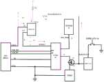
根据本发明的一个方面,提供了一种终端复位电路,该电路如图1所示,包括:复位输入10、处理器11、控制开关12、充电IC 13,充电插座14、电池15、系统电源16和过压保护电路OVP 17;According to one aspect of the present invention, a terminal reset circuit is provided. As shown in FIG. 1 , the circuit includes: a reset input 10, a
其中,复位输入10与处理器11的一个输入引脚连接,处理器11的另一输出引脚与控制开关12的控制端口连接,该处理器11的另一输出引脚还连接在OVP17的使能端连接,;Among them, the reset input 10 is connected to an input pin of the
处理器11用于在接收到复位输入10的复位信号后,将该复位信号通过另一输出引脚输出;The
所述控制开关12用于在接收到输入信号后关断(即关断两个连接端的电连接);The
所述OVP17,用于在使能端接收到输入信号后关断。The OVP17 is used to turn off after the enable terminal receives the input signal.
可选的,上述控制开关12为PMOS管或PNP三极管。Optionally, the above-mentioned
需要说明的是,上述输入引脚与另一输出引脚均可以为处理器的通用输入输出引脚,上述处理器根据不同型号的终端,可能有所不同,例如A10、A9等等处理芯片。It should be noted that both the above-mentioned input pin and another output pin can be general-purpose input and output pins of the processor, and the above-mentioned processor may be different according to different types of terminals, such as A10, A9 and other processing chips.
可选的,上述OVP17包括:输入端(IN)、输出端(OUT)和使能端(OVLO),该输入端(IN)充电插座14连接(具体可以为VBUS接口),该输出端(OUT)与充电IC 13的充电端口连接,充电IC13与系统电源16连接,使能端OVLO与处理器11的复位输入10连接。Optionally, the above OVP17 includes: an input end (IN), an output end (OUT) and an enable end (OVLO), the input end (IN) is connected to the charging socket 14 (specifically, it may be a VBUS interface), the output end (OUT) ) is connected to the charging port of the charging
其工作原理可以为,对于OVP来说,如果手机处于正常充电的状态,即使能端(OVLO)输入电压为低电平(例如零),此时OVP导通,充电插座14的VBUS端口通过OVP17以及充电IC13为所述系统电源16供电,当接收到用户的复位信号后,复位信号输出一高电平,该高电平具体可以为1.2V,高电平输入到使能端(OVLO),OVP关断切断充电插座14的供电,达到复位。Its working principle can be, for OVP, if the mobile phone is in a normal charging state, even if the input voltage of the enable terminal (OVLO) is low level (for example, zero), the OVP is turned on at this time, and the VBUS port of the charging socket 14 passes through the OVP17. And the charging
可选的,上述复位电路还可以包括:保护电阻R10,该保护电阻R10的一端连接使能端(OVLO),另一端接地,设置保护电阻R10的目的是为了避免复位信号的电压过高对OVP损坏,具有提高电路安全性的优点。Optionally, the above reset circuit may also include: a protection resistor R10, one end of the protection resistor R10 is connected to the enable terminal (OVLO), and the other end is grounded. The purpose of setting the protection resistor R10 is to prevent the reset signal from being too high to OVP. damage, has the advantage of improving circuit safety.
可选的,上述复位电路还可以包括:第一电容C1和第二电容C2,第一电容C1的一端连接OVP的输入端(IN),第一电容C1的另一端接地,第二电容C2的一端连接OVP的输出端(OUT),C2的另一端接地。在OVP的输入和输出设置电容是为了让输入电压或输出电压保持稳定,具有稳压和滤波的作用。Optionally, the above reset circuit may further include: a first capacitor C1 and a second capacitor C2, one end of the first capacitor C1 is connected to the input terminal (IN) of the OVP, the other end of the first capacitor C1 is grounded, and the second capacitor C2 is connected to the ground. One end is connected to the output end (OUT) of OVP, and the other end of C2 is grounded. Capacitors are set at the input and output of OVP to keep the input voltage or output voltage stable, and have the functions of voltage regulation and filtering.
下面通过图2来说明两种状态下的复位实现方式。The reset implementation manners in the two states are described below with reference to FIG. 2 .
状态1、仅电池供电。当用户执行复位需求时,如图2箭头所示,电源是由电池供电,因此只要PMOS关断即可实现复位操作。由于处理器在接收到复位指令后,将输出一个高电平,该电平只要满足PMOS关断条件即可,一般为电池电压,因此PMOS由于栅源电压或者栅漏电压低于门槛电压而关断,及系统电源VPH_PWR与电池断开也就实现了复位操作。State 1. Battery powered only. When the user performs the reset request, as shown by the arrow in Figure 2, the power supply is powered by the battery, so as long as the PMOS is turned off, the reset operation can be realized. Since the processor will output a high level after receiving the reset command, the level only needs to meet the PMOS turn-off condition, which is generally the battery voltage. Therefore, the PMOS is turned off because the gate-source voltage or gate-drain voltage is lower than the threshold voltage. , and the system power supply VPH_PWR is disconnected from the battery to realize the reset operation.
状态2(参阅图3)、供电状态时,此时供电为充电供电以及电池供电2个,电池供电的切断可以参见状态1的描述,这里不再赘述,这里仅说明充电供电的切断,由于处理器在接收到复位指令后,将输出一个高电平,该高电平会输入到过压保护电路(具体的电路原理图如图5所示)17,过压保护电路启动过压保护,切断充电(即VBUS)供电从而达到切断电源的达到电源复位的作用。In state 2 (refer to Figure 3) and the power supply state, the power supply is charging power supply and battery power supply at this time. For the cutoff of battery power supply, please refer to the description of state 1, which will not be repeated here. Only the cutoff of charging power supply will be described here. After receiving the reset command, the device will output a high level, which will be input to the overvoltage protection circuit (the specific circuit schematic diagram is shown in Figure 5) 17. The overvoltage protection circuit starts the overvoltage protection and cuts off the Charging (ie VBUS) to supply power so as to cut off the power and achieve the function of power reset.
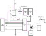
参阅图4,可选的,所述终端复位电路还包括:分压电路,所述分压电路包括:第二电阻和第三电阻,所述第二电阻的一端与所述处理器的另一输出引脚连接,所述第二电阻的另一端连接所述第三电阻的一端,所述第三电阻的另一端接地,所述第二电阻的另一端还与所述使能端连接。Referring to FIG. 4 , optionally, the terminal reset circuit further includes: a voltage divider circuit, the voltage divider circuit includes: a second resistor and a third resistor, one end of the second resistor is connected to the other end of the processor The output pin is connected, the other end of the second resistor is connected to one end of the third resistor, the other end of the third resistor is grounded, and the other end of the second resistor is also connected to the enabling end.
可选的,所述第二电阻与第三电阻的比值小于设定值。Optionally, the ratio of the second resistance to the third resistance is less than a set value.
可选的,所述设定值的范围为【0,0.01】。Optionally, the range of the set value is [0, 0.01].
本发明具体实施方式还提供一种终端,该终端包括如图1所示实施例中的终端复位电路。A specific embodiment of the present invention also provides a terminal, which includes the terminal reset circuit in the embodiment shown in FIG. 1 .
参见图5,本发明实施例还提供一种终端500,该终端500包括但不限于:智能手机、智能手表、平板电脑、个人计算机、笔记本电脑或计算机群组,如图5所示,该终端500包括:处理器501、存储器502、收发器503。收发器503用于与外部设备之间收发数据。终端500中的处理器501的数量可以是一个或多个。本申请的一些实施例中,处理器501、存储器502和收发器503可通过总线系统或其他方式连接。该终端还包括:复位输入10、控制开关12、充电IC13,充电插座14、电池15、处理器501和过压保护电路OVP 17。Referring to FIG. 5, an embodiment of the present invention further provides a terminal 500. The terminal 500 includes but is not limited to: a smart phone, a smart watch, a tablet computer, a personal computer, a notebook computer, or a computer group. As shown in FIG. 5, the terminal 500 includes: a processor 501 , a
其中,复位输入10与微处理器11的一个输入引脚连接,微处理器11的另一输出引脚与控制开关12的控制端口连接,该微处理器11的另一输出引脚还连接在OVP17的使能端连接,;The reset input 10 is connected to an input pin of the
微处理器11用于在接收到复位输入10的复位信号后,将该复位信号通过另一输出引脚输出;The
所述控制开关12用于在接收到输入信号后关断(即关断两个连接端的电连接);The
所述OVP17,用于在使能端接收到输入信号后关断。The OVP17 is used to turn off after the enable terminal receives the input signal.
可选的,上述控制开关12为PMOS管或PNP三极管。Optionally, the above-mentioned
需要说明的是,上述输入引脚与另一输出引脚均可以为微处理器11的通用输入输出引脚,上述微处理器11根据不同型号的终端。It should be noted that, the above-mentioned input pin and another output pin can both be general-purpose input and output pins of the
可选的,上述OVP17包括:输入端(IN)、输出端(OUT)和使能端(OVLO),该输入端(IN)充电插座14连接(具体可以为VBUS接口),该输出端(OUT)与充电IC 13的充电端口连接,充电IC13与处理器501连接,使能端OVLO与微处理器11的复位输入10连接。Optionally, the above OVP17 includes: an input end (IN), an output end (OUT) and an enable end (OVLO), the input end (IN) is connected to the charging socket 14 (specifically, it may be a VBUS interface), the output end (OUT) ) is connected to the charging port of the charging
其工作原理可以为,对于OVP来说,如果手机处于正常充电的状态,即使能端(OVLO)输入电压为低电平(例如零),此时OVP导通,充电插座14的VBUS端口通过OVP17以及充电IC13为所述处理器501供电,当接收到用户的复位信号后,复位信号输出一高电平,该高电平具体可以为1.2V,高电平输入到使能端(OVLO),OVP关断切断充电插座14的供电,达到复位。Its working principle can be, for OVP, if the mobile phone is in a normal charging state, even if the input voltage of the enable terminal (OVLO) is low level (for example, zero), the OVP is turned on at this time, and the VBUS port of the charging socket 14 passes through the OVP17. And the charging
可选的,上述复位电路还可以包括:保护电阻R10,该保护电阻R10的一端连接使能端(OVLO),另一端接地,设置保护电阻R10的目的是为了避免复位信号的电压过高对OVP损坏,具有提高电路安全性的优点。Optionally, the above reset circuit may also include: a protection resistor R10, one end of the protection resistor R10 is connected to the enable terminal (OVLO), and the other end is grounded. The purpose of setting the protection resistor R10 is to prevent the reset signal from being too high to OVP. damage, has the advantage of improving circuit safety.
可选的,上述复位电路还可以包括:第一电容C1和第二电容C2,第一电容C1的一端连接OVP的输入端(IN),第一电容C1的另一端接地,第二电容C2的一端连接OVP的输出端(OUT),C2的另一端接地。在OVP的输入和输出设置电容是为了让输入电压或输出电压保持稳定,具有稳压和滤波的作用。Optionally, the above reset circuit may further include: a first capacitor C1 and a second capacitor C2, one end of the first capacitor C1 is connected to the input terminal (IN) of the OVP, the other end of the first capacitor C1 is grounded, and the second capacitor C2 is connected to the ground. One end is connected to the output end (OUT) of OVP, and the other end of C2 is grounded. Capacitors are set at the input and output of OVP to keep the input voltage or output voltage stable, and have the functions of voltage regulation and filtering.
需要说明的是,这里的处理器501可以是中央处理器(Central Processing Unit,CPU),也可以是特定集成电路(Application Specific Integrated Circuit,ASIC),或者是被配置成实施本申请实施例的一个或多个集成电路,例如:一个或多个微处理器(digital signal processor,DSP),或,一个或者多个现场可编程门阵列(FieldProgrammable Gate Array,FPGA)。It should be noted that the processor 501 here may be a central processing unit (Central Processing Unit, CPU), may also be a specific integrated circuit (Application Specific Integrated Circuit, ASIC), or is configured to implement one of the embodiments of the present application or more integrated circuits, for example: one or more microprocessors (digital signal processors, DSP), or one or more field programmable gate arrays (Field Programmable Gate Array, FPGA).
存储器502可以是一个存储装置,也可以是多个存储元件的统称,且用于存储可执行程序代码或应用程序运行装置运行所需要参数、数据等。且存储器403可以包括随机存储器(RAM),也可以包括非易失性存储器(non-volatile memory),例如磁盘存储器,闪存(Flash)等。The
所属领域的技术人员可以清楚地了解到,为描述的方便和简洁,上述描述的系统、装置和单元的具体工作过程,可以参考前述方法实施例中的对应过程,在此不再赘述。Those skilled in the art can clearly understand that, for the convenience and brevity of description, the specific working process of the above-described systems, devices and units may refer to the corresponding processes in the foregoing method embodiments, which will not be repeated here.
在本申请所提供的几个实施例中,应该理解到,所揭露的系统、装置和方法,可以通过其它的方式实现。以上所描述的装置实施例仅仅是示意性的,例如,所述单元的划分,仅仅为一种逻辑功能划分,实际实现时可以有另外的划分方式,又例如,多个单元或组件可以结合或者可以集成到另一个系统,或一些特征可以忽略,或不执行。另一点,所显示或讨论的相互之间的耦合或直接耦合或通信连接可以是通过一些通信接口,装置或单元的间接耦合或通信连接,可以是电性,机械或其它的形式。In the several embodiments provided in this application, it should be understood that the disclosed system, apparatus and method may be implemented in other manners. The apparatus embodiments described above are only illustrative. For example, the division of the units is only a logical function division. In actual implementation, there may be other division methods. For example, multiple units or components may be combined or Can be integrated into another system, or some features can be ignored, or not implemented. On the other hand, the shown or discussed mutual coupling or direct coupling or communication connection may be through some communication interfaces, indirect coupling or communication connection of devices or units, which may be in electrical, mechanical or other forms.
所述作为分离部件说明的单元可以是或者也可以不是物理上分开的,作为单元显示的部件可以是或者也可以不是物理单元,即可以位于一个地方,或者也可以分布到多个网络单元上。可以根据实际的需要选择其中的部分或者全部单元来实现本实施例方案的目的。The units described as separate components may or may not be physically separated, and components displayed as units may or may not be physical units, that is, may be located in one place, or may be distributed to multiple network units. Some or all of the units may be selected according to actual needs to achieve the purpose of the solution in this embodiment.
另外,在本发明各个实施例中的各功能单元可以集成在一个处理单元中,也可以是各个单元单独物理存在,也可以两个或两个以上单元集成在一个单元中。In addition, each functional unit in each embodiment of the present invention may be integrated into one processing unit, or each unit may exist physically alone, or two or more units may be integrated into one unit.
所述功能如果以软件功能单元的形式实现并作为独立的产品销售或使用时,可以存储在一个计算机可读取存储介质中。基于这样的理解,本发明的技术方案本质上或者说对现有技术做出贡献的部分或者该技术方案的部分可以以软件产品的形式体现出来,该计算机软件产品存储在一个存储介质中,包括若干指令用以使得一台计算机设备(可以是个人计算机,服务器,或者网络设备等)执行本发明各个实施例所述方法的全部或部分步骤。而前述的存储介质包括:U盘、移动硬盘、只读存储器(ROM,Read-Only Memory)、随机存取存储器(RAM,Random Access Memory)、磁碟或者光盘等各种可以存储程序代码的介质。The functions, if implemented in the form of software functional units and sold or used as independent products, may be stored in a computer-readable storage medium. Based on this understanding, the technical solution of the present invention can be embodied in the form of a software product in essence, or the part that contributes to the prior art or the part of the technical solution. The computer software product is stored in a storage medium, including Several instructions are used to cause a computer device (which may be a personal computer, a server, or a network device, etc.) to execute all or part of the steps of the methods described in the various embodiments of the present invention. The aforementioned storage medium includes: U disk, mobile hard disk, Read-Only Memory (ROM, Read-Only Memory), Random Access Memory (RAM, Random Access Memory), magnetic disk or optical disk and other media that can store program codes .
最后应说明的是:以上各实施例仅用以说明本发明的技术方案,而非对其限制;尽管参照前述各实施例对本发明进行了详细的说明,本领域的普通技术人员应当理解:其依然可以对前述各实施例所记载的技术方案进行修改,或者对其中部分或者全部技术特征进行等同替换;而这些修改或者替换,并不使相应技术方案的本质脱离本发明各实施例技术方案的范围,其均应涵盖在本发明的权利要求和说明书的范围当中。Finally, it should be noted that the above embodiments are only used to illustrate the technical solutions of the present invention, but not to limit them; although the present invention has been described in detail with reference to the foregoing embodiments, those of ordinary skill in the art should understand that: The technical solutions described in the foregoing embodiments can still be modified, or some or all of the technical features thereof can be equivalently replaced; and these modifications or replacements do not make the essence of the corresponding technical solutions deviate from the technical solutions of the embodiments of the present invention. The scope of the invention should be included in the scope of the claims and description of the present invention.
Claims (10)
Priority Applications (1)
| Application Number | Priority Date | Filing Date | Title |
|---|---|---|---|
| CN201710202739.4ACN107037866B (en) | 2017-03-30 | 2017-03-30 | Terminal reset circuit and terminal |
Applications Claiming Priority (1)
| Application Number | Priority Date | Filing Date | Title |
|---|---|---|---|
| CN201710202739.4ACN107037866B (en) | 2017-03-30 | 2017-03-30 | Terminal reset circuit and terminal |
Publications (2)
| Publication Number | Publication Date |
|---|---|
| CN107037866A CN107037866A (en) | 2017-08-11 |
| CN107037866Btrue CN107037866B (en) | 2020-01-10 |
Family
ID=59533390
Family Applications (1)
| Application Number | Title | Priority Date | Filing Date |
|---|---|---|---|
| CN201710202739.4AExpired - Fee RelatedCN107037866B (en) | 2017-03-30 | 2017-03-30 | Terminal reset circuit and terminal |
Country Status (1)
| Country | Link |
|---|---|
| CN (1) | CN107037866B (en) |
Families Citing this family (2)
| Publication number | Priority date | Publication date | Assignee | Title |
|---|---|---|---|---|
| CN111585555B (en)* | 2020-05-22 | 2023-11-28 | 广东电网有限责任公司 | Anti-vibration circuit, method and intelligent terminal |
| CN112711318A (en)* | 2020-12-26 | 2021-04-27 | 广东湾区智能终端工业设计研究院有限公司 | Reset control circuit and method and terminal |
Citations (4)
| Publication number | Priority date | Publication date | Assignee | Title |
|---|---|---|---|---|
| CN104682337A (en)* | 2013-11-27 | 2015-06-03 | 成都优游信息技术有限公司 | Overvoltage protection circuit for mobile phone game testing |
| CN205104922U (en)* | 2015-07-22 | 2016-03-23 | 嘉善谦信和电子科技有限公司 | Lithium cell intelligent charging circuit with multiple protect function |
| CN106160094A (en)* | 2016-02-05 | 2016-11-23 | 广东欧珀移动通信有限公司 | Charging system, charging method and power adapter for terminal |
| CN106484061A (en)* | 2015-08-28 | 2017-03-08 | 中兴通讯股份有限公司 | Terminal resets control method, controller and system |
Family Cites Families (1)
| Publication number | Priority date | Publication date | Assignee | Title |
|---|---|---|---|---|
| US8675328B2 (en)* | 2011-02-07 | 2014-03-18 | Aeroflex Plainview, Inc. | Battery charge protection system |
- 2017
- 2017-03-30CNCN201710202739.4Apatent/CN107037866B/ennot_activeExpired - Fee Related
Patent Citations (4)
| Publication number | Priority date | Publication date | Assignee | Title |
|---|---|---|---|---|
| CN104682337A (en)* | 2013-11-27 | 2015-06-03 | 成都优游信息技术有限公司 | Overvoltage protection circuit for mobile phone game testing |
| CN205104922U (en)* | 2015-07-22 | 2016-03-23 | 嘉善谦信和电子科技有限公司 | Lithium cell intelligent charging circuit with multiple protect function |
| CN106484061A (en)* | 2015-08-28 | 2017-03-08 | 中兴通讯股份有限公司 | Terminal resets control method, controller and system |
| CN106160094A (en)* | 2016-02-05 | 2016-11-23 | 广东欧珀移动通信有限公司 | Charging system, charging method and power adapter for terminal |
Also Published As
| Publication number | Publication date |
|---|---|
| CN107037866A (en) | 2017-08-11 |
Similar Documents
| Publication | Publication Date | Title |
|---|---|---|
| CN111697663B (en) | Charging circuit and charging cable | |
| US20200412139A1 (en) | Charge Control Method and Device, and Electronic Device | |
| CN108132401A (en) | Charging abnormity detection method and device, storage medium and mobile terminal | |
| CN107332208B (en) | A protection circuit, a main board protection method and a terminal | |
| CN104505888B (en) | A kind of mobile terminal and charging device | |
| CN104505890A (en) | Mobile terminal | |
| CN109245199A (en) | Charging method, charging unit, power supply provide equipment and terminal to be charged | |
| CN103066969B (en) | A kind of electronic equipment with crash reset function | |
| CN106155258A (en) | The circuit of a kind of power down protection and correlation technique | |
| CN104765466A (en) | Key control method and device for mobile terminal | |
| US11742684B2 (en) | Charging control circuit, charging circuit and charging control method | |
| CN104777891A (en) | A kind of OTG connection control method and connection control device applied to intelligent terminal | |
| CN106786960A (en) | Charge control method, device and terminal | |
| CN107508354A (en) | A kind of charging method and mobile terminal | |
| CN107037866B (en) | Terminal reset circuit and terminal | |
| CN115549232B (en) | Charging method, device, electronic device and keyboard for electronic equipment | |
| CN204376457U (en) | A kind of mobile terminal | |
| JP6537085B2 (en) | Self-loop detection method and apparatus for charging device | |
| CN104461659B (en) | A kind of computer starting method of high reliability | |
| CN105429246A (en) | Circuit and method for automatically disconnecting terminal after full charge | |
| WO2024041427A1 (en) | Battery metering system, electronic device and control method | |
| US11816002B2 (en) | Method for a data backup unit to intelligently charge a mobile device | |
| US20190313339A1 (en) | Wifi power supply switching method, circuit and apparatus, and storage medium | |
| US20130061030A1 (en) | System capable of booting through a universal serial bus device and method thereof | |
| US20200117468A1 (en) | Shutdown sequence of thin clients |
Legal Events
| Date | Code | Title | Description |
|---|---|---|---|
| PB01 | Publication | ||
| PB01 | Publication | ||
| SE01 | Entry into force of request for substantive examination | ||
| SE01 | Entry into force of request for substantive examination | ||
| CB02 | Change of applicant information | Address after:523860 No. 18, Wu Sha Beach Road, Changan Town, Dongguan, Guangdong Applicant after:GUANGDONG OPPO MOBILE TELECOMMUNICATIONS Corp.,Ltd. Address before:523860 No. 18, Wu Sha Beach Road, Changan Town, Dongguan, Guangdong Applicant before:GUANGDONG OPPO MOBILE TELECOMMUNICATIONS Corp.,Ltd. | |
| CB02 | Change of applicant information | ||
| GR01 | Patent grant | ||
| GR01 | Patent grant | ||
| CF01 | Termination of patent right due to non-payment of annual fee | Granted publication date:20200110 | |
| CF01 | Termination of patent right due to non-payment of annual fee |