CN107016964B - Pixel circuit, method of driving the same, and display device - Google Patents
Pixel circuit, method of driving the same, and display deviceDownload PDFInfo
- Publication number
- CN107016964B CN107016964BCN201710278367.3ACN201710278367ACN107016964BCN 107016964 BCN107016964 BCN 107016964BCN 201710278367 ACN201710278367 ACN 201710278367ACN 107016964 BCN107016964 BCN 107016964B
- Authority
- CN
- China
- Prior art keywords
- transistor
- sub
- pixel
- scan
- line
- Prior art date
- Legal status (The legal status is an assumption and is not a legal conclusion. Google has not performed a legal analysis and makes no representation as to the accuracy of the status listed.)
- Active
Links
Images


Classifications
- G—PHYSICS
- G09—EDUCATION; CRYPTOGRAPHY; DISPLAY; ADVERTISING; SEALS
- G09G—ARRANGEMENTS OR CIRCUITS FOR CONTROL OF INDICATING DEVICES USING STATIC MEANS TO PRESENT VARIABLE INFORMATION
- G09G3/00—Control arrangements or circuits, of interest only in connection with visual indicators other than cathode-ray tubes
- G09G3/20—Control arrangements or circuits, of interest only in connection with visual indicators other than cathode-ray tubes for presentation of an assembly of a number of characters, e.g. a page, by composing the assembly by combination of individual elements arranged in a matrix no fixed position being assigned to or needed to be assigned to the individual characters or partial characters
- G09G3/22—Control arrangements or circuits, of interest only in connection with visual indicators other than cathode-ray tubes for presentation of an assembly of a number of characters, e.g. a page, by composing the assembly by combination of individual elements arranged in a matrix no fixed position being assigned to or needed to be assigned to the individual characters or partial characters using controlled light sources
- G09G3/30—Control arrangements or circuits, of interest only in connection with visual indicators other than cathode-ray tubes for presentation of an assembly of a number of characters, e.g. a page, by composing the assembly by combination of individual elements arranged in a matrix no fixed position being assigned to or needed to be assigned to the individual characters or partial characters using controlled light sources using electroluminescent panels
- G09G3/32—Control arrangements or circuits, of interest only in connection with visual indicators other than cathode-ray tubes for presentation of an assembly of a number of characters, e.g. a page, by composing the assembly by combination of individual elements arranged in a matrix no fixed position being assigned to or needed to be assigned to the individual characters or partial characters using controlled light sources using electroluminescent panels semiconductive, e.g. using light-emitting diodes [LED]
- G09G3/3208—Control arrangements or circuits, of interest only in connection with visual indicators other than cathode-ray tubes for presentation of an assembly of a number of characters, e.g. a page, by composing the assembly by combination of individual elements arranged in a matrix no fixed position being assigned to or needed to be assigned to the individual characters or partial characters using controlled light sources using electroluminescent panels semiconductive, e.g. using light-emitting diodes [LED] organic, e.g. using organic light-emitting diodes [OLED]
- G09G3/3225—Control arrangements or circuits, of interest only in connection with visual indicators other than cathode-ray tubes for presentation of an assembly of a number of characters, e.g. a page, by composing the assembly by combination of individual elements arranged in a matrix no fixed position being assigned to or needed to be assigned to the individual characters or partial characters using controlled light sources using electroluminescent panels semiconductive, e.g. using light-emitting diodes [LED] organic, e.g. using organic light-emitting diodes [OLED] using an active matrix
- G09G3/3258—Control arrangements or circuits, of interest only in connection with visual indicators other than cathode-ray tubes for presentation of an assembly of a number of characters, e.g. a page, by composing the assembly by combination of individual elements arranged in a matrix no fixed position being assigned to or needed to be assigned to the individual characters or partial characters using controlled light sources using electroluminescent panels semiconductive, e.g. using light-emitting diodes [LED] organic, e.g. using organic light-emitting diodes [OLED] using an active matrix with pixel circuitry controlling the voltage across the light-emitting element
- G—PHYSICS
- G09—EDUCATION; CRYPTOGRAPHY; DISPLAY; ADVERTISING; SEALS
- G09G—ARRANGEMENTS OR CIRCUITS FOR CONTROL OF INDICATING DEVICES USING STATIC MEANS TO PRESENT VARIABLE INFORMATION
- G09G3/00—Control arrangements or circuits, of interest only in connection with visual indicators other than cathode-ray tubes
- G09G3/20—Control arrangements or circuits, of interest only in connection with visual indicators other than cathode-ray tubes for presentation of an assembly of a number of characters, e.g. a page, by composing the assembly by combination of individual elements arranged in a matrix no fixed position being assigned to or needed to be assigned to the individual characters or partial characters
- G09G3/22—Control arrangements or circuits, of interest only in connection with visual indicators other than cathode-ray tubes for presentation of an assembly of a number of characters, e.g. a page, by composing the assembly by combination of individual elements arranged in a matrix no fixed position being assigned to or needed to be assigned to the individual characters or partial characters using controlled light sources
- G09G3/30—Control arrangements or circuits, of interest only in connection with visual indicators other than cathode-ray tubes for presentation of an assembly of a number of characters, e.g. a page, by composing the assembly by combination of individual elements arranged in a matrix no fixed position being assigned to or needed to be assigned to the individual characters or partial characters using controlled light sources using electroluminescent panels
- G09G3/32—Control arrangements or circuits, of interest only in connection with visual indicators other than cathode-ray tubes for presentation of an assembly of a number of characters, e.g. a page, by composing the assembly by combination of individual elements arranged in a matrix no fixed position being assigned to or needed to be assigned to the individual characters or partial characters using controlled light sources using electroluminescent panels semiconductive, e.g. using light-emitting diodes [LED]
- G09G3/3208—Control arrangements or circuits, of interest only in connection with visual indicators other than cathode-ray tubes for presentation of an assembly of a number of characters, e.g. a page, by composing the assembly by combination of individual elements arranged in a matrix no fixed position being assigned to or needed to be assigned to the individual characters or partial characters using controlled light sources using electroluminescent panels semiconductive, e.g. using light-emitting diodes [LED] organic, e.g. using organic light-emitting diodes [OLED]
- G09G3/3225—Control arrangements or circuits, of interest only in connection with visual indicators other than cathode-ray tubes for presentation of an assembly of a number of characters, e.g. a page, by composing the assembly by combination of individual elements arranged in a matrix no fixed position being assigned to or needed to be assigned to the individual characters or partial characters using controlled light sources using electroluminescent panels semiconductive, e.g. using light-emitting diodes [LED] organic, e.g. using organic light-emitting diodes [OLED] using an active matrix
- G09G3/3233—Control arrangements or circuits, of interest only in connection with visual indicators other than cathode-ray tubes for presentation of an assembly of a number of characters, e.g. a page, by composing the assembly by combination of individual elements arranged in a matrix no fixed position being assigned to or needed to be assigned to the individual characters or partial characters using controlled light sources using electroluminescent panels semiconductive, e.g. using light-emitting diodes [LED] organic, e.g. using organic light-emitting diodes [OLED] using an active matrix with pixel circuitry controlling the current through the light-emitting element
- G—PHYSICS
- G09—EDUCATION; CRYPTOGRAPHY; DISPLAY; ADVERTISING; SEALS
- G09G—ARRANGEMENTS OR CIRCUITS FOR CONTROL OF INDICATING DEVICES USING STATIC MEANS TO PRESENT VARIABLE INFORMATION
- G09G2300/00—Aspects of the constitution of display devices
- G09G2300/08—Active matrix structure, i.e. with use of active elements, inclusive of non-linear two terminal elements, in the pixels together with light emitting or modulating elements
- G09G2300/0809—Several active elements per pixel in active matrix panels
- G09G2300/0819—Several active elements per pixel in active matrix panels used for counteracting undesired variations, e.g. feedback or autozeroing
- G—PHYSICS
- G09—EDUCATION; CRYPTOGRAPHY; DISPLAY; ADVERTISING; SEALS
- G09G—ARRANGEMENTS OR CIRCUITS FOR CONTROL OF INDICATING DEVICES USING STATIC MEANS TO PRESENT VARIABLE INFORMATION
- G09G2310/00—Command of the display device
- G09G2310/02—Addressing, scanning or driving the display screen or processing steps related thereto
- G09G2310/0264—Details of driving circuits
- G09G2310/0281—Arrangement of scan or data electrode driver circuits at the periphery of a panel not inherent to a split matrix structure
- G—PHYSICS
- G09—EDUCATION; CRYPTOGRAPHY; DISPLAY; ADVERTISING; SEALS
- G09G—ARRANGEMENTS OR CIRCUITS FOR CONTROL OF INDICATING DEVICES USING STATIC MEANS TO PRESENT VARIABLE INFORMATION
- G09G2320/00—Control of display operating conditions
- G09G2320/02—Improving the quality of display appearance
- G09G2320/0233—Improving the luminance or brightness uniformity across the screen
- G—PHYSICS
- G09—EDUCATION; CRYPTOGRAPHY; DISPLAY; ADVERTISING; SEALS
- G09G—ARRANGEMENTS OR CIRCUITS FOR CONTROL OF INDICATING DEVICES USING STATIC MEANS TO PRESENT VARIABLE INFORMATION
- G09G2320/00—Control of display operating conditions
- G09G2320/02—Improving the quality of display appearance
- G09G2320/029—Improving the quality of display appearance by monitoring one or more pixels in the display panel, e.g. by monitoring a fixed reference pixel
- G09G2320/0295—Improving the quality of display appearance by monitoring one or more pixels in the display panel, e.g. by monitoring a fixed reference pixel by monitoring each display pixel
Landscapes
- Engineering & Computer Science (AREA)
- Physics & Mathematics (AREA)
- Computer Hardware Design (AREA)
- General Physics & Mathematics (AREA)
- Theoretical Computer Science (AREA)
- Electroluminescent Light Sources (AREA)
- Control Of El Displays (AREA)
- Control Of Indicators Other Than Cathode Ray Tubes (AREA)
Abstract
Translated fromChinese
Description
Translated fromChinese技术领域technical field
本发明涉及显示技术领域,具体来说涉及一种像素电路、其驱动方法和显示装置。The present invention relates to the field of display technology, and in particular, to a pixel circuit, a driving method thereof and a display device.
背景技术Background technique
在有源矩阵有机发光二极管(AMOLED)显示器中,各像素中的相应驱动晶体管可能具有不同的特性(例如,不同的迁移率或阈值电压),使得各像素在相同的灰阶电压下呈现不同的亮度。这种亮度的不均匀性被称为“mura”。补偿技术可以用来缓解mura效果,其中外部电学补偿是一种常用的技术,尤其是在大尺寸OLED显示器中。外部电学补偿可以涉及使用感测线将驱动晶体管生成的饱和电流(下文中也称为“像素电流”)汲取到外部补偿电路,该外部补偿电路然后基于像素电流的量值与目标值的差异确定补偿数据,并向驱动电路提供对应于目标亮度的经补偿的显示数据。In an active-matrix organic light-emitting diode (AMOLED) display, the corresponding drive transistors in each pixel may have different characteristics (eg, different mobilities or threshold voltages), so that each pixel appears different at the same grayscale voltage brightness. This unevenness in brightness is called "mura". Compensation techniques can be used to mitigate the mura effect, of which external electrical compensation is a commonly used technique, especially in large-size OLED displays. External electrical compensation may involve using sense lines to draw the saturation current generated by the drive transistor (hereinafter also referred to as "pixel current") to an external compensation circuit, which then determines based on the difference in magnitude of the pixel current from a target value The compensation data is provided, and the compensated display data corresponding to the target luminance is provided to the driving circuit.
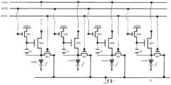
图1示出了一种其中可以实现外部电学补偿的现有OLED 像素电路的示意图。如所示的,该像素电路包括四个子像素,其包括相应的开关晶体管 SW1,SW2,SW3,SW4、相应的驱动晶体管DR1,DR2,DR3,DR4、相应的感测晶体管SE1,SE2,SE3,SE4、相应的存储电容器Cst、以及相应的有机发光二极管OLED1,OLED2,OLED3,OLED4。开关晶体管 SW1,SW2,SW3和SW4分别连接到数据线DATA1,DATA2,DATA3和DATA4,并且在来自第二扫描线GATE2的扫描信号的控制下操作。驱动晶体管DR1,DR2,DR3和DR4连接到电源线ELVDD。感测晶体管SE1,SE2,SE3和SE4在来自第一扫描线GATE1的扫描信号的控制下操作。为了提高开口率,这四个感测晶体管SE1,SE2,SE3和SE4(以及潜在地更多像素电路的感测晶体管)连接到一条公共的感测线SL。在这种情况下,感测线SL上呈现的电容Cap至少包括1)由于感测线SL与其他金属导线或金属块的交叠而形成的电容,以及2)连接到感测线SL的感测晶体管SE1,SE2,SE3和SE4的寄生电容(栅源/栅漏电容)。尤其是,在感测晶体管SE1,SE2,SE3和SE4具有底栅结构的情况下,寄生的栅源电容和栅漏电容会比较大(与其中各感测晶体管具有顶栅结构的情况相比)。Figure 1 shows a schematic diagram of a conventional OLED pixel circuit in which external electrical compensation can be implemented. As shown, the pixel circuit includes four sub-pixels including corresponding switch transistors SW1, SW2, SW3, SW4, corresponding drive transistors DR1, DR2, DR3, DR4, corresponding sense transistors SE1, SE2, SE3, SE4, the corresponding storage capacitor Cst, and the corresponding organic light emitting diodes OLED1, OLED2, OLED3, OLED4. The switching transistors SW1, SW2, SW3 and SW4 are connected to the data lines DATA1, DATA2, DATA3 and DATA4, respectively, and operate under the control of the scan signal from the second scan line GATE2. The drive transistors DR1, DR2, DR3 and DR4 are connected to the power supply line ELVDD. The sensing transistors SE1, SE2, SE3 and SE4 operate under the control of the scan signal from the first scan line GATE1. To increase the aperture ratio, the four sense transistors SE1 , SE2 , SE3 and SE4 (and potentially the sense transistors of more pixel circuits) are connected to a common sense line SL. In this case, the capacitance Cap presented on the sensing line SL includes at least 1) the capacitance formed by the overlapping of the sensing line SL with other metal wires or metal blocks, and 2) the capacitance connected to the sensing line SL Measure the parasitic capacitance (gate-source/gate-drain capacitance) of transistors SE1, SE2, SE3 and SE4. In particular, in the case where the sense transistors SE1, SE2, SE3 and SE4 have a bottom gate structure, the parasitic gate-source capacitance and gate-drain capacitance will be relatively large (compared to the case where each sense transistor has a top gate structure) .
感测线SL从像素汲取的像素电流可以由通过该像素电流对感测线SL上呈现的电容Cap充电而生成的电压来指示。因此,感测线SL上呈现的总电容Cap是影响补偿准确性的因素之一。总电容Cap越大,要求充电电流越大并且充电时间越长。大的充电电流意味着大的数据电压,其可能超出正常的显示电压范围。而且,长的充电时间在其中要求实时补偿的场景下可能不能得以满足,导致对电容Cap的充电不足并且因此降低的补偿精度。The pixel current drawn by the sense line SL from the pixel may be indicated by the voltage generated by charging the capacitance Cap present on the sense line SL with this pixel current. Therefore, the total capacitance Cap presented on the sense line SL is one of the factors affecting the compensation accuracy. The larger the total capacitance Cap, the larger the required charging current and the longer the charging time. A large charging current means a large data voltage, which may exceed the normal display voltage range. Also, long charging times may not be satisfied in scenarios where real-time compensation is required, resulting in insufficient charging of the capacitor Cap and thus reduced compensation accuracy.
发明内容SUMMARY OF THE INVENTION
有利的是提供一种可以缓解或减轻上述问题中的至少一个的像素电路。同样期望的是提供一种包括这样的像素电路的显示装置和驱动这样的像素电路的方法。It would be advantageous to provide a pixel circuit that alleviates or mitigates at least one of the above problems. It is also desirable to provide a display device including such a pixel circuit and a method of driving such a pixel circuit.
根据本发明的第一方面,提供了一种像素电路,包括:多个子像素,每个包括:有机发光二极管,具有阳极;驱动晶体管,经由所述阳极与所述有机发光二极管串联;以及感测晶体管,具有连接到所述阳极的第一电极、连接到第一扫描线的栅极、以及第二电极。该像素电路还包括公共晶体管,具有连接到所述多个子像素的各感测晶体管的第二电极的第一电极、连接到所述第一扫描线的栅极、以及连接到感测线的第二电极。According to a first aspect of the present invention, there is provided a pixel circuit comprising: a plurality of sub-pixels, each comprising: an organic light emitting diode having an anode; a driving transistor connected in series with the organic light emitting diode via the anode; and a sensing A transistor has a first electrode connected to the anode, a gate connected to the first scan line, and a second electrode. The pixel circuit further includes a common transistor having a first electrode connected to the second electrode of each sensing transistor of the plurality of sub-pixels, a gate connected to the first scan line, and a first electrode connected to the sense line Two electrodes.
在一些实施例中,所述多个子像素被配置成使得当在补偿模式下所述多个子像素之一被供应有数据电压时该子像素的驱动晶体管基于所述数据电压生成饱和电流。所述被供应有数据电压的子像素的感测晶体管和所述公共晶体管被配置成在所述补偿模式下响应于来自所述第一扫描线的第一扫描信号将所生成的饱和电流传送给所述感测线以供检测。In some embodiments, the plurality of subpixels are configured such that when one of the plurality of subpixels is supplied with a data voltage in a compensation mode, a drive transistor of the subpixel generates a saturation current based on the data voltage. The sensing transistor of the sub-pixel supplied with the data voltage and the common transistor are configured to transmit the generated saturation current to the compensation mode in response to the first scan signal from the first scan line. the sense lines for detection.
在一些实施例中,所述多个子像素中的每个还包括:存储电容器,具有连接到所述驱动晶体管的栅极的第一端和连接到所述驱动晶体管的源极的第二端;以及开关晶体管,具有连接到数据线的第一电极、连接到第二扫描线的栅极、以及连接到所述存储电容器的第一端的第二电极。In some embodiments, each of the plurality of subpixels further includes: a storage capacitor having a first end connected to the gate of the drive transistor and a second end connected to the source of the drive transistor; and a switching transistor having a first electrode connected to a data line, a gate connected to a second scan line, and a second electrode connected to a first end of the storage capacitor.
在一些实施例中,所述驱动晶体管为N型晶体管,并且所述驱动晶体管的所述源极和所述存储电容器的第二端连接到所述有机发光二极管的阳极。In some embodiments, the drive transistor is an N-type transistor, and the source of the drive transistor and the second end of the storage capacitor are connected to the anode of the organic light emitting diode.
在一些实施例中,所述多个子像素的各感测晶体管和所述公共晶体管被配置成当参考电压被施加到所述感测线时响应于所述第一扫描信号将所述参考电压传送到所述多个子像素的各存储电容器的第二端。In some embodiments, the respective sense transistors and the common transistor of the plurality of sub-pixels are configured to transmit the reference voltage in response to the first scan signal when the reference voltage is applied to the sense line to the second ends of the respective storage capacitors of the plurality of sub-pixels.
在一些实施例中,所述驱动晶体管为P型晶体管,并且所述驱动晶体管的漏极连接到所述有机发光二极管的阳极。In some embodiments, the drive transistor is a P-type transistor, and the drain of the drive transistor is connected to the anode of the organic light emitting diode.
在一些实施例中,所述公共晶体管为底栅型晶体管。In some embodiments, the common transistor is a bottom gate transistor.
在一些实施例中,所述像素电路包括用于RGBW像素图案的四个子像素或者用于RGB像素图案的三个子像素。In some embodiments, the pixel circuit includes four sub-pixels for an RGBW pixel pattern or three sub-pixels for an RGB pixel pattern.
根据本发明的第二方面,提供了一种显示装置,包括:第一扫描驱动器,用于向多条第一扫描线顺序地供应第一扫描信号;第二扫描驱动器,用于向多条第二扫描线顺序地供应第二扫描信号;数据驱动器,用于基于图像数据生成数据信号并且向多条数据线供应所生成的数据信号;多个像素电路,每个包括多个子像素,所述多个像素电路呈阵列布置使得所述多个像素电路的各子像素呈行和列布置,每行子像素连接到所述多条第一扫描线中的相应一条和所述多条第二扫描线中的相应一条,每列子像素连接到所述多条数据线中的相应一条,每个子像素包括:有机发光二极管,具有阳极;驱动晶体管,经由所述阳极与所述有机发光二极管串联;以及感测晶体管,具有连接到所述阳极的第一电极、连接到该行子像素所连接的该第一扫描线的栅极、以及第二电极,每列像素电路连接到多条感测线中的相应一条,每个像素电路还包括公共晶体管,其具有连接到所述多个子像素的各感测晶体管的第二电极的第一电极、连接到该行子像素所连接的该第一扫描线的栅极、以及连接到该列像素电路所连接的该感测线的第二电极。所述显示装置还包括多个采样电路,每个连接到所述多条感测线中的相应一条,每个采样电路被配置成对通过由所述相应的感测线传送的像素电流对该感测线上呈现的电容充电而生成的电压进行采样;以及时序控制器,用于控制所述第一扫描驱动器、所述第二扫描驱动器、所述数据驱动器和所述多个采样电路的操作并且基于所述多个采样电路的采样对提供给所述数据驱动器的所述图像数据进行补偿。According to a second aspect of the present invention, there is provided a display device, comprising: a first scan driver for sequentially supplying a first scan signal to a plurality of first scan lines; a second scan driver for supplying a plurality of first scan lines Two scan lines sequentially supply second scan signals; a data driver for generating data signals based on image data and supplying the generated data signals to a plurality of data lines; a plurality of pixel circuits each including a plurality of sub-pixels, the plurality of The pixel circuits are arranged in an array such that sub-pixels of the plurality of pixel circuits are arranged in rows and columns, and each row of sub-pixels is connected to a corresponding one of the plurality of first scan lines and the plurality of second scan lines A corresponding one of the sub-pixels, each column of sub-pixels is connected to a corresponding one of the plurality of data lines, and each sub-pixel includes: an organic light emitting diode having an anode; a driving transistor connected in series with the organic light emitting diode via the anode; a sensing transistor, having a first electrode connected to the anode, a gate connected to the first scan line to which the row of sub-pixels is connected, and a second electrode, each column of pixel circuits is connected to one of the plurality of sensing lines Correspondingly, each pixel circuit further includes a common transistor having a first electrode connected to the second electrode of each sensing transistor of the plurality of sub-pixels, a first electrode connected to the first scan line to which the row of sub-pixels is connected a gate, and a second electrode connected to the sensing line to which the column of pixel circuits is connected. The display device also includes a plurality of sampling circuits, each connected to a corresponding one of the plurality of sense lines, each sampling circuit configured to pair a pixel current transmitted by the corresponding sense line to the corresponding one. sampling a voltage generated by charging a capacitor present on a sensing line; and a timing controller for controlling operations of the first scan driver, the second scan driver, the data driver and the plurality of sampling circuits And the image data supplied to the data driver is compensated based on the sampling of the plurality of sampling circuits.
在一些实施例中,所述多个采样电路中的每个包括第一受控开关和模数转换器。所述第一受控开关被配置成响应于第一开关控制信号将所述生成的电压耦合到所述模数转换器,并且所述模数转换器被配置成将所述生成的电压转换成数字值并将该数字值提供给所述时序控制器。In some embodiments, each of the plurality of sampling circuits includes a first controlled switch and an analog-to-digital converter. The first controlled switch is configured to couple the generated voltage to the analog-to-digital converter in response to a first switch control signal, and the analog-to-digital converter is configured to convert the generated voltage into digital value and provide the digital value to the timing controller.
在一些实施例中,所述驱动晶体管为N型晶体管,并且所述多个采样电路中的每个还包括第二受控开关,其被配置成响应于第二开关控制信号将参考电压源供应的参考电压施加到所述感测线。In some embodiments, the drive transistor is an N-type transistor, and each of the plurality of sampling circuits further includes a second controlled switch configured to supply the reference voltage source in response to the second switch control signal The reference voltage is applied to the sense line.
在一些实施例中,每个像素电路的所述多个子像素的各感测晶体管和所述公共晶体管被配置成当所述参考电压被施加到所述感测线时响应于来自所述第一扫描线的第一扫描信号将所述参考电压传送到各所述感测晶体管的第一电极。In some embodiments, the respective sense transistors and the common transistors of the plurality of sub-pixels of each pixel circuit are configured to respond to signals from the first when the reference voltage is applied to the sense line The first scan signal of the scan line transmits the reference voltage to the first electrodes of each of the sensing transistors.
在一些实施例中,每个像素电路的所述多个子像素中的每个还包括:存储电容器,具有连接到所述驱动晶体管的栅极的第一端和连接到所述驱动晶体管的源极的第二端;以及开关晶体管,具有连接到该列子像素所连接的该数据线的第一电极、连接到该行子像素所连接的该第二扫描线的栅极、以及连接到所述存储电容器的第一端的第二电极。In some embodiments, each of the plurality of subpixels of each pixel circuit further includes a storage capacitor having a first end connected to the gate of the drive transistor and a source connected to the drive transistor and a switching transistor having a first electrode connected to the data line connected to the column of subpixels, a gate connected to the second scan line connected to the row of subpixels, and connected to the storage the second electrode of the first end of the capacitor.
在一些实施例中,所述驱动晶体管为N型晶体管,并且所述驱动晶体管的所述源极和所述存储电容器的第二端连接到所述有机发光二极管的阳极。In some embodiments, the drive transistor is an N-type transistor, and the source of the drive transistor and the second end of the storage capacitor are connected to the anode of the organic light emitting diode.
在一些实施例中,所述驱动晶体管为P型晶体管,并且所述驱动晶体管的漏极连接到所述有机发光二极管的阳极。In some embodiments, the drive transistor is a P-type transistor, and the drain of the drive transistor is connected to the anode of the organic light emitting diode.
在一些实施例中,所述公共晶体管为底栅型晶体管。In some embodiments, the common transistor is a bottom gate transistor.
在一些实施例中,每个像素电路包括用于RGBW像素图案的四个子像素或者用于RGB像素图案的三个子像素。In some embodiments, each pixel circuit includes four sub-pixels for an RGBW pixel pattern or three sub-pixels for an RGB pixel pattern.
根据本发明的第三方面,提供了一种驱动像素电路的方法。所述像素电路包括多个子像素,每个包括:有机发光二极管,具有阳极;驱动晶体管,经由所述阳极与所述有机发光二极管串联;以及感测晶体管,具有连接到所述阳极的第一电极、连接到第一扫描线的栅极、以及第二电极;公共晶体管,具有连接到所述多个子像素的各感测晶体管的第二电极的第一电极、连接到所述第一扫描线的栅极、以及连接到感测线的第二电极;存储电容器,具有连接到所述驱动晶体管的栅极的第一端和连接到所述驱动晶体管的源极的第二端;以及开关晶体管,具有连接到数据线的第一电极、连接到第二扫描线的栅极、以及连接到所述存储电容器的第一端的第二电极。所述方法包括:在向连接到所述多个子像素的相应数据线之一供应数据信号的同时将来自所述第二扫描线的第二扫描信号施加到所述多个子像素的各开关晶体管的栅极,以将来自该数据线的数据信号传送到该数据线所连接的子像素的所述存储电容器的第一端;通过将来自所述第一扫描线的第一扫描信号施加到所述多个子像素的各感测晶体管的栅极和所述公共晶体管的栅极,将由该子像素的所述驱动晶体管基于所述数据信号生成的饱和电流传送到所述感测线,所述饱和电流对所述感测线上呈现的电容充电;以及经由所述感测线将通过所述饱和电流对所述电容充电而生成的电压传送到外部电路以供检测。According to a third aspect of the present invention, a method of driving a pixel circuit is provided. The pixel circuit includes a plurality of sub-pixels, each including: an organic light emitting diode having an anode; a drive transistor connected in series with the organic light emitting diode via the anode; and a sense transistor having a first electrode connected to the anode , a gate connected to the first scan line, and a second electrode; a common transistor having a first electrode connected to the second electrode of each sensing transistor of the plurality of sub-pixels, a gate connected to the first scan line a gate, and a second electrode connected to the sense line; a storage capacitor having a first end connected to the gate of the drive transistor and a second end connected to the source of the drive transistor; and a switch transistor, There is a first electrode connected to a data line, a gate connected to a second scan line, and a second electrode connected to a first end of the storage capacitor. The method includes applying a second scan signal from the second scan line to each switching transistor of the plurality of subpixels while supplying a data signal to one of the corresponding data lines connected to the plurality of subpixels. gate to transmit the data signal from the data line to the first end of the storage capacitor of the sub-pixel connected to the data line; by applying the first scan signal from the first scan line to the a gate of each sensing transistor of a plurality of sub-pixels and a gate of the common transistor transmit a saturation current generated by the driving transistor of the sub-pixel based on the data signal to the sensing line, the saturation current charging a capacitance present on the sense line; and transmitting a voltage generated by charging the capacitance with the saturation current via the sense line to an external circuit for detection.
在一些实施例中,所述驱动晶体管为N型晶体管,所述驱动晶体管的所述源极和所述存储电容器的第二端连接到所述有机发光二极管的阳极,并且所述方法还包括:与将所述第二扫描信号施加到各所述开关晶体管的栅极同时地,通过将所述第一扫描信号施加到所述多个子像素的各感测晶体管的栅极和所述公共晶体管的栅极,将施加到所述感测线的参考电压传送到该子像素的所述存储电容器的第二端。In some embodiments, the drive transistor is an N-type transistor, the source of the drive transistor and the second end of the storage capacitor are connected to the anode of the organic light emitting diode, and the method further includes: Simultaneously with applying the second scan signal to the gate of each of the switching transistors, by applying the first scan signal to the gate of each of the sensing transistors of the plurality of sub-pixels and the gate of the common transistor a gate that transmits the reference voltage applied to the sense line to the second end of the storage capacitor of the sub-pixel.
在一些实施例中,所述方法还包括:在将所述像素电流传送到所述感测线的同时,使所述第二扫描信号无效以关断所述开关晶体管。In some embodiments, the method further includes deasserting the second scan signal to turn off the switching transistor while delivering the pixel current to the sense line.
在一些实施例中,所述方法,还包括:在将所述像素电流传送到所述感测线的同时,使所述第二扫描信号保持有效以将所述数据信号持续施加到所述存储电容器的第一端。In some embodiments, the method further includes maintaining the second scan signal active to continuously apply the data signal to the memory while delivering the pixel current to the sense line the first end of the capacitor.
根据在下文中所描述的实施例,本发明的这些和其它方面将是清楚明白的,并且将参考在下文中所描述的实施例而被阐明。These and other aspects of the invention will be apparent from and elucidated with reference to the embodiments described hereinafter.
附图说明Description of drawings
图1示出了一种其中可以实现外部电学补偿的现有OLED 像素电路的示意图;FIG. 1 shows a schematic diagram of a conventional OLED pixel circuit in which external electrical compensation can be implemented;
图2示出了根据本发明实施例的显示装置的框图;FIG. 2 shows a block diagram of a display device according to an embodiment of the present invention;
图3示出了图2的显示装置中包括的时序控制器的框图;3 shows a block diagram of a timing controller included in the display device of FIG. 2;
图4示出了根据本发明实施例的像素电路的电路图;FIG. 4 shows a circuit diagram of a pixel circuit according to an embodiment of the present invention;
图5是图4的像素电路在发光模式下的时序图;5 is a timing diagram of the pixel circuit of FIG. 4 in a light-emitting mode;
图6是图4的像素电路在补偿模式下的时序图;6 is a timing diagram of the pixel circuit of FIG. 4 in a compensation mode;
图7是图4的像素电路在另一补偿模式下的时序图;并且FIG. 7 is a timing diagram of the pixel circuit of FIG. 4 in another compensation mode; and
图8示出了根据本发明另一实施例的像素电路的电路图。FIG. 8 shows a circuit diagram of a pixel circuit according to another embodiment of the present invention.
具体实施方式Detailed ways
将理解的是,尽管术语第一、第二、第三等等在本文中可以用来描述各种元件、部件和/或部分,但是这些元件、部件和/或部分不应当由这些术语限制。这些术语仅用来将一个元件、部件或部分与另一个元件、部件或部分相区分。因此,下面讨论的第一元件、部件或部分可以被称为第二元件、部件或部分而不偏离本发明的教导。It will be understood that, although the terms first, second, third, etc. may be used herein to describe various elements, components and/or sections, these elements, components and/or sections should not be limited by these terms. These terms are only used to distinguish one element, component or section from another element, component or section. Thus, a first element, component or section discussed below could be termed a second element, component or section without departing from the teachings of the present invention.
本文中使用的术语仅出于描述特定实施例的目的并且不意图限制本发明。如本文中使用的,单数形式“一个”、“一”和“该”意图也包括复数形式,除非上下文清楚地另有指示。将进一步理解的是,术语“包括”和/或“包含”当在本说明书中使用时指定所述及特征、整体、步骤、操作、元件和/或部件的存在,但不排除一个或多个其他特征、整体、步骤、操作、元件、部件和/或其群组的存在或添加一个或多个其他特征、整体、步骤、操作、元件、部件和/或其群组。如本文中使用的,术语“和/或”包括相关联的列出项目中的一个或多个的任意和全部组合。The terminology used herein is for the purpose of describing particular embodiments only and is not intended to limit the invention. As used herein, the singular forms "a," "an," and "the" are intended to include the plural forms as well, unless the context clearly dictates otherwise. It will be further understood that the terms "comprising" and/or "comprising" when used in this specification designate the presence of stated features, integers, steps, operations, elements and/or parts, but do not exclude one or more The presence or addition of one or more other features, integers, steps, operations, elements, components, and/or groups thereof, of other features, integers, steps, operations, elements, components, and/or groups thereof. As used herein, the term "and/or" includes any and all combinations of one or more of the associated listed items.
将理解的是,当元件被称为“连接到另一个元件”或“耦合到另一个元件”时,其可以直接连接到另一个元件或直接耦合到另一个元件,或者可以存在中间元件。相反,当元件被称为“直接连接到另一个元件”、“直接耦合到另一个元件”时,没有中间元件存在。此外,短语“基于”意图被解释为“至少部分地基于”,除非明确地另有说明。It will be understood that when an element is referred to as being "connected to" or "coupled to" another element, it can be directly connected or coupled to the other element or intervening elements may be present. In contrast, when an element is referred to as being "directly connected to" or "directly coupled to" another element, there are no intervening elements present. Further, the phrase "based on" is intended to be construed as "based at least in part on" unless expressly stated otherwise.
除非另有定义,本文中使用的所有术语(包括技术术语和科学术语)具有与本发明所属领域的普通技术人员所通常理解的相同含义。将进一步理解的是,诸如那些在通常使用的字典中定义的之类的术语应当被解释为具有与其在相关领域和/或本说明书上下文中的含义相一致的含义,并且将不在理想化或过于正式的意义上进行解释,除非本文中明确地如此定义。Unless otherwise defined, all terms (including technical and scientific terms) used herein have the same meaning as commonly understood by one of ordinary skill in the art to which this invention belongs. It will be further understood that terms such as those defined in commonly used dictionaries should be construed to have meanings consistent with their meanings in the relevant art and/or the context of this specification, and will not be idealized or overly interpreted in a formal sense, unless expressly defined as such herein.
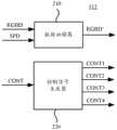
图2示出了根据本发明实施例的显示装置100的框图。参见图2,显示装置100包括像素阵列110、第一扫描驱动器102、第二扫描驱动器 104、数据驱动器106、多个采样电路SP1,SP2,…,SPm、电源108和时序控制器112。FIG. 2 shows a block diagram of a
像素阵列110包括n×m个像素电路P。每个像素电路P包括OLED和多个子像素(图2中未示出)。像素阵列110包括在行方向上布置以传送第一扫描信号的n条第一扫描线GATE1[1],GATE1[2],...,GATE1[n];在行方向上布置以传送第二扫描信号的n条第二扫描线GATE2[1],GATE2[2],...,GATE2[n];在列方向上布置以传送数据信号的m组数据线D[1],D[2],...,D[m];在列方向上布置以从各像素电路P汲取像素电流的m条感测线SL[1],SL[2],...,SL[m];以及用于施加电源电压ELVDD的电线(未示出)。n和m是自然数。取决于每个像素电路P包括的子像素的数目,数据线组D[1],D[2],...,D[m]中的每个可以包括与子像素的数目相同的数目的数据线以用于向各个子像素供应相应的数据信号。n×m个像素电路P呈阵列布置使得各像素电路P的各子像素呈行和列布置。每行子像素连接到n条第一扫描线中的相应一条和n条第二扫描线中的相应一条,并且每列子像素连接到各数据线中的相应一条。另外,每列像素电路P连接到感测线SL[1],SL[2],...,SL[m]中的相应一条。The
第一扫描驱动器102连接至第一扫描线GATE1[1],GATE1[2],...,GATE1[n],以将第一扫描信号施加至像素阵列110。第二扫描驱动器104连接至第二扫描线GATE2[1],GATE2[2],...,GATE2[n],以将第二扫描信号施加至像素阵列110。数据驱动器106连接至数据线组D[1],D[2],...,D[m],以将数据信号施加至像素阵列110。采样电路SP1,SP2,…,SPm分别连接到感测线SL[1],SL[2],...,SL[m],以对通过从各像素电路P汲取的像素电流对感测线SL[1],SL[2],...,SL[m]上呈现的电容充电而生成的电压进行采样。电源108供应的电源电压ELVDD(图2中未示出)被施加至像素阵列110中的每个像素电路P。The
时序控制器112用于控制第一扫描驱动器102、第二扫描驱动器104、数据驱动器106和采样电路SP1,SP2,…,SPm的操作。时序控制器112从外部设备(例如,主机)接收输入图像数据RGBD和输入控制信号CONT,并且从采样电路SP1,SP2,…,SPm接收采样数据SPD。输入图像数据RGBD可包括用于多个像素的多个输入像素数据。每个输入像素数据可包括用于多个像素中的相应一个的红色灰度数据R、绿色灰度数据G和蓝色灰度数据B。输入控制信号CONT可包括主时钟信号、数据使能信号、垂直同步信号、水平同步信号等。时序控制器112还从采样电路SP1,SP2,…,SPm接收采样数据SPD。时序控制器112基于输入图像数据RGBD、采样数据SPD和输入控制信号CONT 生成输出图像数据RGBD’、第一控制信号CONT1、第二控制信号 CONT2、第三控制信号CONT3和第四控制信号 CONT4。The
具体地,时序控制器112可基于输入图像数据RGBD和采样数据SPD生成输出图像数据RGBD’。输出图像数据RGBD’可以是通过使用补偿算法补偿输入图像数据RGBD 而生成的补偿图像数据。具体的补偿算法超出了本文中讨论的范围,并且可以是本领域中任何已知或将来的技术。输出图像数据RGBD’可包括用于多个像素的多个输出像素数据,并且被提供给数据驱动器106。时序控制器112可基于输入控制信号CONT生成第一控制信号 CONT1和第二控制信号CONT2。第一控制信号CONT1和第二控制信号CONT2可被分别提供给第一扫描驱动器102和第二扫描驱动器104,并且第一扫描驱动器102和第二扫描驱动器104的驱动时序可分别基于第一控制信号CONT1和第二控制信号CONT2被控制。第一控制信号CONT1和第二控制信号CONT2可包括垂直启动信号、栅极时钟信号等。时序控制器112还可基于输入控制信号CONT生成第三控制信号CONT3和第四控制信号CONT4。第三控制信号CONT3可被提供给数据驱动器106,并且数据驱动器106的驱动时序可基于第三控制信号CONT3被控制。第三控制信号CONT3 可包括水平启动信号、数据时钟信号、数据负载信号、极性控制信号等。第四控制信号CONT4可被提供给各采样电路SP1,SP2,…,SPm,并且采样电路SP1,SP2,…,SPm的驱动时序可基于第四控制信号CONT4被控制。例如,采样电路SP1,SP2,…,SPm可被控制使得在补偿模式下在像素电流对感测线SL[1],SL[2],...,SL[m]上呈现的电容充电完成后对所述电容上的电压进行采样。Specifically, the
第一扫描驱动器102和第二扫描驱动器104从时序控制器112分别接收第一控制信号CONT1和第二控制信号CONT2。第一扫描驱动器102基于第一控制信号CONT1生成顺序地施加到第一扫描线GATE1[1],GATE1[2],...,GATE1[n]的多个栅极信号。第二扫描驱动器104基于第二控制信号CONT2生成顺序地施加到第二扫描线GATE2[1],GATE2[2],...,GATE2[n]的多个栅极信号。The
数据驱动器106从时序控制器112接收第三控制信号CONT3和输出图像数据RGBD’。数据驱动器106基于第三控制信号CONT3和输出图像数据RGBD’(例如,数字图像数据)生成多个数据信号(例如,模拟灰阶电压)。数据驱动器106可将多个数据信号施加至数据线组D[1],D[2],...,D[m]的各数据线。The data driver 106 receives the third control signal CONT3 from the
采样电路SP1,SP2,…,SPm连接到相应的感测线SL[1],SL[2],...,SL[m]并且从时序控制器112接收第四控制信号CONT4。采样电路SP1,SP2,…,SPm中的每个基于第四控制信号CONT4对通过由相应的感测线传送的像素电流对所述感测线上呈现的电容充电而生成的电压进行采样。给定所述电容的值和充电时间,所生成的电压可以指示像素电流的量值。The sampling circuits SP1, SP2, . . . , SPm are connected to the corresponding sensing lines SL[1], SL[2], . . . , SL[m] and receive the fourth control signal CONT4 from the
图3示出了图2的显示装置100中包括的时序控制器112的框图。FIG. 3 shows a block diagram of the
参考图3,时序控制器112可包括数据补偿器210和控制信号生成器220。为了方便描述,时序控制器112在图3中示出为被划分成两个元件,尽管时序控制器112可不被物理划分。Referring to FIG. 3 , the
数据补偿器210可基于来自所述多个采样电路SP1,SP2,…,SPm的采样数据SPD对输入图像数据RGBD进行补偿以便生成经补偿的输出图像数据RGBD’。The data compensator 210 may compensate the input image data RGBD based on the sampled data SPD from the plurality of sampling circuits SP1, SP2, . . . , SPm to generate compensated output image data RGBD'.
控制信号生成器220可从外部设备接收输入控制信号CONT,并且可基于输入控制信号CONT生成用于图2中的各控制信号CONT1,CONT2,CONT3和CONT4。控制信号生成器220可将第一控制信号CONT1输出至图2中的第一扫描驱动器102,将第二控制信号CONT2输出至图2中的第二扫描驱动器104,将第三控制信号CONT3输出至图2中的数据驱动器106,并且将第四控制信号CONT4输出至图2中的采样电路SP1,SP2,…,SPm。The
作为示例而非限制,在上面的实施例中,显示装置100可以为手机、平板电脑、电视机、显示器、笔记本电脑、数码相框、导航仪等任何具有显示功能的产品或部件。As an example and not a limitation, in the above embodiments, the
图4示出了根据本发明实施例的像素电路的电路图。为了便于描述,示出了连接到第n条第一扫描线GATE1[n]、第n条第二扫描线GATE2[n]、第m组数据线D[m]和第m条感测线SL[m]的像素电路。FIG. 4 shows a circuit diagram of a pixel circuit according to an embodiment of the present invention. For convenience of description, connections to the n-th first scan line GATE1[n], the n-th second scan line GATE2[n], the m-th group of data lines D[m], and the m-th sensing line SL are shown. [m] pixel circuit.
在图4的示例中,像素电路包括四个子像素,其包括相应的有机发光二极管OLED1,OLED2,OLED3,OLED4、相应的驱动晶体管DR1,DR2,DR3,DR4和相应的感测晶体管SE1,SE2,SE3,SE4。连接到该像素电路的数据线组包括四条数据线DATA1,DATA2,DATA3和DATA4,其分别向四个子像素供应数据信号。这四个子像素可以被设计成具有相同的结构并且显示不同的颜色分量(例如用于RGBW像素图案)。以第一个子像素为例,驱动晶体管DR1经由有机发光二极管OLED1的阳极与有机发光二极管OLED1串联,并且感测晶体管SE1具有连接到所述阳极的第一电极、连接到第一扫描线GATE1[n]的栅极、以及第二电极。该子像素还包括存储电容器Cst和开关晶体管SW1。存储电容器Cst具有连接到驱动晶体管DR1的栅极的第一端和连接到驱动晶体管DR1的源极的第二端。开关晶体管SW1具有连接到数据线DATA1的第一电极、连接到第二扫描线GATE2[n]的栅极、以及连接到存储电容器Cst的第一端的第二电极。开关晶体管SW1可以响应于来自第二扫描线GATE2[n]的第二扫描信号将来自数据线DATA1的数据信号传送到存储电容器Cst的第一端。In the example of FIG. 4, the pixel circuit includes four sub-pixels including corresponding organic light emitting diodes OLED1, OLED2, OLED3, OLED4, corresponding driving transistors DR1, DR2, DR3, DR4 and corresponding sensing transistors SE1, SE2, SE3, SE4. The data line group connected to the pixel circuit includes four data lines DATA1, DATA2, DATA3, and DATA4, which supply data signals to four sub-pixels, respectively. The four sub-pixels can be designed to have the same structure and display different color components (eg for RGBW pixel patterns). Taking the first sub-pixel as an example, the driving transistor DR1 is connected in series with the organic light emitting diode OLED1 via the anode of the organic light emitting diode OLED1, and the sensing transistor SE1 has a first electrode connected to the anode, connected to the first scan line GATE1[ n] gate, and the second electrode. The subpixel also includes a storage capacitor Cst and a switching transistor SW1. The storage capacitor Cst has a first terminal connected to the gate of the driving transistor DR1 and a second terminal connected to the source of the driving transistor DR1. The switching transistor SW1 has a first electrode connected to the data line DATA1, a gate electrode connected to the second scan line GATE2[n], and a second electrode connected to the first end of the storage capacitor Cst. The switching transistor SW1 may transfer the data signal from the data line DATA1 to the first end of the storage capacitor Cst in response to the second scan signal from the second scan line GATE2[n].
像素电路还包括公共晶体管COM,其具有连接到各子像素的感测晶体管SE1,SE2,SE3,SE4的第二电极的第一电极、连接到第一扫描线GATE1[n]的栅极、以及连接到感测线SL[m]的第二电极。各子像素被配置成使得当在补偿模式下所述各子像素之一被供应有数据电压时该子像素的驱动晶体管基于所述数据电压生成饱和电流。被供应有数据电压的该子像素的感测晶体管和公共晶体管COM被配置成在所述补偿模式下响应于来自第一扫描线GATE1[n]的第一扫描信号将所生成的饱和电流传送给感测线SL[m]以供检测。The pixel circuit also includes a common transistor COM having a first electrode connected to the second electrode of the sensing transistors SE1, SE2, SE3, SE4 of each sub-pixel, a gate connected to the first scan line GATE1[n], and Connected to the second electrode of the sense line SL[m]. Each sub-pixel is configured such that when one of the sub-pixels is supplied with the data voltage in the compensation mode, the drive transistor of the sub-pixel generates a saturation current based on the data voltage. The sensing transistor of the sub-pixel supplied with the data voltage and the common transistor COM are configured to transmit the generated saturation current to the compensation mode in response to the first scan signal from the first scan line GATE1[n]. Sense line SL[m] for detection.
如图4所示,代替直接连接到各子像素的感测晶体管SE1,SE2,SE3,SE4,感测线SL[m]经由公共晶体管COM连接到各子像素。因此,感测线SL[m]上呈现的电容Cap包括1)由于感测线SL[m]与其他金属导线或金属块的交叠而形成的电容,以及2)公共晶体管COM的寄生电容。就寄生电容而言,将连接到感测线SL[m]的一列像素的所有公共晶体管COM的寄生电容考虑在内,总的寄生电容可以简单地计算为1×Cp×Nr,其中Cp为单个晶体管的寄生电容(栅源电容或栅漏电容),并且Nr为像素阵列中像素的行数。相比之下,在如图1所示的像素电路的情况下,感测线SL上呈现的总的寄生电容为4×Cp×Nr,因为感测线SL被连接到四个感测晶体管SE1,SE2,SE3和SE4。由于在根据本发明实施例的像素电路中连接到感测线的晶体管的数目大大减少,感测线上呈现的电容可以被大大减小。这对于提高外部电学补偿的准确性是有利的。另外,用于驱动公共晶体管COM的栅极信号可以与用于驱动感测晶体管SE1,SE2,SE3,SE4的栅极信号(即, 来自第一扫描线GATE1[n]的第一扫描信号)相同,所以无需增加新的控制逻辑。这可以导致电路的低的复杂度。As shown in FIG. 4 , instead of the sensing transistors SE1 , SE2 , SE3 , SE4 directly connected to the respective sub-pixels, the sensing line SL[m] is connected to the respective sub-pixels via a common transistor COM. Therefore, the capacitance Cap presented on the sensing line SL[m] includes 1) the capacitance formed by the overlapping of the sensing line SL[m] and other metal wires or metal blocks, and 2) the parasitic capacitance of the common transistor COM. In terms of parasitic capacitance, taking into account the parasitic capacitances of all common transistors COM of a column of pixels connected to the sense line SL[m], the total parasitic capacitance can be simply calculated as 1 × Cp × Nr, where Cp is a single The parasitic capacitance of the transistor (gate-source capacitance or gate-drain capacitance), and Nr is the number of rows of pixels in the pixel array. In contrast, in the case of the pixel circuit as shown in FIG. 1 , the total parasitic capacitance presented on the sense line SL is 4×Cp×Nr because the sense line SL is connected to the four sense transistors SE1 , SE2, SE3 and SE4. Since the number of transistors connected to the sensing line is greatly reduced in the pixel circuit according to the embodiment of the present invention, the capacitance present on the sensing line can be greatly reduced. This is advantageous for improving the accuracy of external electrical compensation. In addition, the gate signal for driving the common transistor COM may be the same as the gate signal for driving the sensing transistors SE1, SE2, SE3, SE4 (ie, the first scan signal from the first scan line GATE1[n]) , so there is no need to add new control logic. This can lead to a low complexity of the circuit.
在各实施例中,像素电路中的公共晶体管COM(以及潜在地其他晶体管)可以是底栅型晶体管。尽管底栅型晶体管具有比顶栅型晶体管更大的寄生电容,但是在根据本发明实施例的像素电路中感测线上呈现的电容仍然可以较小,因为感测线经由单个公共晶体管连接到各子像素,而不是直接连接到各子像素的多个感测晶体管。还设想了其他实施例。例如,像素电路中的公共晶体管COM(以及潜在地其他晶体管)可以是顶栅型晶体管。In various embodiments, the common transistor COM (and potentially other transistors) in the pixel circuit may be a bottom gate type transistor. Although bottom-gate transistors have larger parasitic capacitances than top-gate transistors, the capacitances present on the sense lines can still be smaller in pixel circuits according to embodiments of the present invention, because the sense lines are connected via a single common transistor to each sub-pixel, rather than the multiple sense transistors directly connected to each sub-pixel. Other embodiments are also contemplated. For example, the common transistor COM (and potentially other transistors) in the pixel circuit may be a top-gate transistor.
继续图4的示例,感测线SL[m]连接到采样电路SPm,其对通过经由感测晶体管SE1,SE2,SE3或SE4以及公共晶体管COM传送的饱和电流对电容Cap充电而生成的电压进行采样。采样电路SPm包括第一受控开关SA和模数转换器ADC。第一受控开关SA可以响应于第一开关控制信号将所述生成的电压耦合到模数转换器ADC。模数转换器ADC可以将所述生成的电压转换成数字值并将该数字值提供给图2中的时序控制器112。Continuing with the example of FIG. 4 , the sense line SL[m] is connected to the sampling circuit SPm, which performs a voltage generated by charging the capacitor Cap by the saturation current delivered through the sense transistors SE1 , SE2 , SE3 or SE4 and the common transistor COM sampling. The sampling circuit SPm includes a first controlled switch SA and an analog-to-digital converter ADC. The first controlled switch SA may couple the generated voltage to the analog-to-digital converter ADC in response to the first switch control signal. An analog-to-digital converter ADC may convert the generated voltage to a digital value and provide the digital value to the
在图4的示例中,像素电路中的各驱动晶体管DR1,DR2,DR3,DR4被示出为N型晶体管。在这种情况下,驱动晶体管DR1,DR2,DR3,DR4的源极和相应的存储电容器Cst的第二端连接到相应的有机发光二极管OLED1,OLED2,OLED3,OLED4的阳极,并且采样电路SPm还包括第二受控开关EN,其可以响应于第二开关控制信号将参考电压源Vref供应的参考电压施加到感测线SL[m]。如下面描述的,当数据电压要被写入子像素时,该参考电压可以通过公共晶体管COM和相应的感测晶体管SE1,SE2,SE3,SE4耦合到相应的存储电容器Cst的第二端。耦合到存储电容器Cst的第二端的该参考电压连同耦合到该存储电容器Cst的第一端的数据信号一起确定由该存储电容器Cst存储的数据电压(即跨驱动晶体管DR1,DR2,DR3或DR4的栅极和源极的电压)。In the example of FIG. 4, the respective drive transistors DR1, DR2, DR3, DR4 in the pixel circuit are shown as N-type transistors. In this case, the sources of the driving transistors DR1, DR2, DR3, DR4 and the second terminals of the corresponding storage capacitors Cst are connected to the anodes of the corresponding organic light emitting diodes OLED1, OLED2, OLED3, OLED4, and the sampling circuit SPm is also A second controlled switch EN is included, which can apply a reference voltage supplied by the reference voltage source Vref to the sense line SL[m] in response to a second switch control signal. As described below, when the data voltage is to be written into the sub-pixel, the reference voltage may be coupled to the second terminal of the corresponding storage capacitor Cst through the common transistor COM and the corresponding sensing transistors SE1, SE2, SE3, SE4. The reference voltage coupled to the second terminal of the storage capacitor Cst, along with the data signal coupled to the first terminal of the storage capacitor Cst, determines the data voltage stored by the storage capacitor Cst (ie, the voltage across the drive transistor DR1, DR2, DR3 or DR4). gate and source voltages).
下面结合图5-7描述图4的像素电路的操作,其中图5涉及该像素电路在发光模式下的操作,并且图6和7涉及该像素电路在补偿模式下的操作。The operation of the pixel circuit of Fig. 4 is described below in conjunction with Figs. 5-7, wherein Fig. 5 relates to the operation of the pixel circuit in the light emission mode, and Figs. 6 and 7 relate to the operation of the pixel circuit in the compensation mode.
图5是图4的像素电路在发光模式下的时序图。FIG. 5 is a timing diagram of the pixel circuit of FIG. 4 in a light-emitting mode.
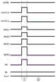
在阶段①中,相应的数据电压被写入各存储电容器Cst。来自第二扫描线GATE2[n]的第二扫描信号(图5中为高电平电压)被施加到开关晶体管SW1,SW2,SW3和SW4的栅极,使得数据线DATA1,DATA2,DATA3和DATA4上的数据信号被传送到各存储电容器Cst的第一端。来自第一扫描线GATE1[n]的第一扫描信号(图5中为高电平电压)被施加到感测晶体管SE1,SE2,SE3,SE4和公共晶体管COM的栅极,并且第二开关控制信号(图5中为高电平电压)被施加到第二受控开关EN,使得参考电压源Vref供应的参考电压被施加到感测线SL[m],并且进而通过公共晶体管COM和相应的感测晶体管SE1,SE2,SE3,SE4被传送到相应的存储电容器Cst的第二端。由此,各存储电容器Cst存储相应的数据电压。In
在阶段②中,各驱动晶体管DR1,DR2,DR3,DR4驱动相应的有机发光二极管OLED1,OLED2,OLED3,OLED4发光。根据晶体管的饱和电流公式,驱动晶体管生成的像素电流可以计算为:In
I = 1/2*u*Cox*(W/L)(Vgs-Vth)2(1)I = 1/2*u*Cox*(W/L)(Vgs-Vth)2 (1)
其中u为电子的迁移率,Cox为单位面积栅氧化层电容,W/L是驱动晶体管的沟道宽长比,Vgs为跨驱动晶体管的栅极和源极的电压,并且Vth为驱动晶体管的阈值电压。由于第一扫描线GATE1[n]上的第一扫描信号在阶段②中被无效(deactivated)(其跳变至低电平,如图5中所示),所以各感测晶体管SE1,SE2,SE3,SE4和公共晶体管COM被关断。因此,各驱动晶体管DR1,DR2,DR3,DR4生成的像素电流流过相应的有机发光二极管OLED1,OLED2,OLED3,OLED4,而不会被汲取到感测线SL[m]。where u is the mobility of electrons, Cox is the gate oxide capacitance per unit area, W/L is the channel width to length ratio of the drive transistor, Vgs is the voltage across the gate and source of the drive transistor, and Vth is the drive transistor’s threshold voltage. Since the first scan signal on the first scan line GATE1[n] is deactivated in phase ② (it jumps to a low level, as shown in FIG. 5 ), the respective sensing transistors SE1 , SE2 , SE3, SE4 and the common transistor COM are turned off. Therefore, the pixel current generated by each of the driving transistors DR1, DR2, DR3, DR4 flows through the corresponding organic light emitting diodes OLED1, OLED2, OLED3, OLED4 without being drawn to the sensing line SL[m].
图6是图4的像素电路在补偿模式下的时序图。FIG. 6 is a timing diagram of the pixel circuit of FIG. 4 in a compensation mode.
在阶段①中,一个数据电压被写入该像素电路的多个子像素之一。如图6所示,向连接到该多个子像素的相应数据线之一(图6中为DATA1)供应数据信号,并且同时将来自第二扫描线GATE2[n]的第二扫描信号施加到多个子像素的各开关晶体管SW1,SW2,SW3,SW4的栅极。因此,来自数据线DATA1的数据信号被传送到与该数据线DATA1连接的子像素的存储电容器Cst的第一端。In
在其中驱动晶体管DR1为N型晶体管并且因此驱动晶体管DR1的源极和存储电容器Cst的第二端连接到有机发光二极管OLED1的阳极的情况下,在阶段①中还可以向各存储电容器Cst的第二端提供参考电压(例如,低电平电压)。如图6所示,在阶段①中第二开关控制信号被施加到第二受控开关EN,使得参考电压源Vref供应的参考电压被施加到感测线SL[m]。与将第二扫描信号施加到各开关晶体管SW1,SW2,SW3,SW4的栅极同时地,通过将来自第一扫描线GATE1[n]的第一扫描信号施加到各感测晶体管SE1,SE2,SE3,SE4的栅极和所述公共晶体管COM的栅极,施加到感测线SL[m]的参考电压被传送到各存储电容器Cst的第二端。在图6的示例中,来自数据线DATA1的数据信号和由参考电压源Vref供应的该参考电压一起确定第一个子像素的存储电容器Cst所存储的数据电压(即,跨驱动晶体管DR1的栅极和源极的电压)。补偿模式下的参考电压可以不等于发光模式下的参考电压。In the case where the drive transistor DR1 is an N-type transistor and thus the source of the drive transistor DR1 and the second end of the storage capacitor Cst are connected to the anode of the organic light emitting diode OLED1, it is also possible in
在阶段②中,由在阶段①中被写入有数据电压的子像素生成像素电流,并且该像素电流被汲取到感测线SL[m],从而对感测线SL[m]上呈现的电容Cap充电。在图6的示例中,驱动晶体管DR1按照上面的等式(1)生成像素电流。来自第一扫描线GATE1[n]的第一扫描信号被施加到各感测晶体管SE1,SE2,SE3,SE4的栅极和公共晶体管COM的栅极,使得各感测晶体管SE1,SE2,SE3,SE4和公共晶体管COM被导通。因此,驱动晶体管DR1生成的像素电流通过感测晶体管SE1和公共晶体管COM被传送到感测线SL[m],对感测线SL[m]上呈现的电容Cap充电。在充电期间,电容Cap上的电压Vsense逐渐升高。In
在图6的示例中,第二扫描线GATE2[n]上的第二扫描信号在阶段②中被无效,使得开关晶体管SW1被关断。因此,存储电容器Cst的第一端被悬浮。在这种情况下,由于存储电容器Cst的自举(self-boosting)效应,即使电容Cap上的电压Vsense(并且因此存储电容器Cst的第二端处的电压)逐渐升高,跨存储电容器Cst的电压也保持为在阶段①中写入的数据电压。In the example of FIG. 6 , the second scan signal on the second scan line GATE2[n] is deactivated in
将理解的是,在阶段②中驱动晶体管DR1生成的像素电流不会流过有机发光二极管OLED1,而是通过(导通的)感测晶体管SE1和公共晶体管COM被传送到感测线SL[m]。这是因为1)有机发光二极管OLED1的等效电阻远大于导通的感测晶体管SE1和公共晶体管COM的等效电阻,并且2)电压Vsense一般小于有机发光二极管OLED1的阈值电压。因此,像素电流沿着“驱动晶体管DR1-感测晶体管SE1-公共晶体管COM-感测线SL[m]”的路径流动,而不流过有机发光二极管OLED1。It will be understood that the pixel current generated by the drive transistor DR1 in
在阶段③中,对电容Cap的充电完成,并且得到的电压Vsense被采样并传送到外部电路以供检测。具体地,如图6所示,第一扫描线GATE1[n]上的第一扫描信号在阶段③中被无效,使得各感测晶体管SE1,SE2,SE3,SE4和公共晶体管COM被关断。同时,第一开关控制信号(图6中为高电平电压)被施加到采样电路SPm中的第一受控开关SA,使得电压Vsense被耦合到采样电路SPm中的模数转换器ADC以供采样,并且所采样的数字值被传送到诸如图2中的时序控制器112之类的外部电路。如上面描述的,电压Vsense可以指示像素电流的量值。时序控制器112然后可以基于像素电流的量值与目标值的差异确定补偿数据,并向图2中的数据驱动器106提供对应于目标亮度的经补偿的图像数据。具体的补偿机制超出了本文中讨论的范围。In
在阶段④中,可以经由相应的数据线DATA1,DATA2,DATA3和DATA4向各子像素写入数据信号。在图6的示例中,施加到每个子像素的数据电压(即,跨驱动晶体管DR1,DR2,DR3或DR4的栅极和源极)被置零。还设想了其他实施例。例如,图6中所示的操作可以在帧周期的空白(Blank)时段中执行,并且因此可以在显示装置的正常操作期间实时地发生。具体地,在当前帧周期的空白时段中获取的采样数据被用于对下一帧周期中的图像数据进行补偿。在这种情况下,可以在阶段④中将当前帧周期中用于各子像素的数据电压写回到各子像素中,以便防止显示画面的闪烁。In stage ④, data signals may be written to each sub-pixel via the corresponding data lines DATA1, DATA2, DATA3 and DATA4. In the example of Figure 6, the data voltage applied to each sub-pixel (ie, across the gate and source of the drive transistor DR1, DR2, DR3 or DR4) is zeroed. Other embodiments are also contemplated. For example, the operations shown in FIG. 6 may be performed in blank periods of the frame period, and thus may occur in real time during normal operation of the display device. Specifically, the sampling data acquired in the blank period of the current frame period is used to compensate the image data in the next frame period. In this case, the data voltage for each sub-pixel in the current frame period can be written back to each sub-pixel in phase ④, in order to prevent flickering of the display screen.
图7是图4的像素电路在另一补偿模式下的时序图。FIG. 7 is a timing diagram of the pixel circuit of FIG. 4 in another compensation mode.
与图6中所示的操作相比,在其中像素电流被传送到感测线SL[m]的阶段②中,第二扫描线GATE2[n]上的第二扫描信号被保持有效以将数据线DATA1上的数据信号持续施加到存储电容器Cst的第一端。随着电容Cap上的电压Vsense(并且因此存储电容器Cst的第二端处的电压)逐渐升高,跨存储电容器Cst的电压(即,跨驱动晶体管DR1的栅极和源极的电压)逐渐减小,使得驱动晶体管DR1生成的像素电流也逐渐减小。这导致对电容Cap的充电的速率的下降。正因为如此,如图7所示,电容Cap上的电压Vsense以逐渐减小的斜率缓慢升高,直到跨存储电容器Cst的电压减小到驱动晶体管DR1的阈值电压为止。此时,驱动晶体管DR1处于介于截止和饱和的临界状态,并且生成的像素电流可以被认为等于零。对电容Cap的充电然后得以完成。Compared with the operation shown in FIG. 6, in the
在图7的示例中,花费如此长的时间来对电容Cap充电,使得图7中所示的操作可能无法在显示装置的正常操作期间实时地执行。因此,在一些实施例中,图7中所示的操作可以在其中显示装置未处于正常操作的状态(例如,待机状态)下执行,尽管这不是必须的。在这种情况下,通过执行图7中所示的操作而获取的采样数据可以用于当显示装置处于正常操作时对每个帧周期中的图像数据进行补偿。In the example of FIG. 7 , it takes so long to charge the capacitor Cap that the operations shown in FIG. 7 may not be performed in real time during normal operation of the display device. Accordingly, in some embodiments, the operations shown in FIG. 7 may be performed in a state in which the display device is not in normal operation (eg, a standby state), although this is not required. In this case, the sampling data acquired by performing the operations shown in FIG. 7 can be used to compensate the image data in each frame period when the display apparatus is in normal operation.
在像素电路的以上各实施例中,各驱动晶体管、各开关晶体管、各感测晶体管以及公共晶体管被示出为N型晶体管。然而,本发明不限于此。在其他实施例中,这些晶体管中的至少一个可以是P型晶体管。In the above embodiments of the pixel circuit, the drive transistors, the switch transistors, the sense transistors, and the common transistor are shown as N-type transistors. However, the present invention is not limited to this. In other embodiments, at least one of these transistors may be a P-type transistor.
图8示出了根据本发明另一实施例的像素电路的电路图。FIG. 8 shows a circuit diagram of a pixel circuit according to another embodiment of the present invention.
如图8所示,在该像素电路中,各驱动晶体管DR1,DR2,DR3和DR4为P型晶体管。各驱动晶体管DR1,DR2,DR3,DR4的漏极连接到相应的有机发光二极管OLED1,OLED2,OLED3,OLED4的阳极,并且各驱动晶体管DR1,DR2,DR3,DR4的源极和各存储电容器Cst的第二端连接到电源电压ELVDD。由于各存储电容器Cst的第二端连接到固定的电源电压ELVDD,在数据写入阶段①中无需向各存储电容器Cst提供参考电压。在这种情况下,采样电路SPm可以未被提供有用于将参考电压源Vref供应的参考电压耦合到感测线SL[m]的第二受控开关EN。As shown in FIG. 8, in this pixel circuit, each of the driving transistors DR1, DR2, DR3 and DR4 is a P-type transistor. The drain of each driving transistor DR1, DR2, DR3, DR4 is connected to the anode of the corresponding organic light emitting diode OLED1, OLED2, OLED3, OLED4, and the source of each driving transistor DR1, DR2, DR3, DR4 and each storage capacitor Cst The second terminal is connected to the power supply voltage ELVDD. Since the second terminal of each storage capacitor Cst is connected to the fixed power supply voltage ELVDD, it is not necessary to supply a reference voltage to each storage capacitor Cst in the
将理解的是,图8的像素电路是示例性的,并且在其他实施例中开关晶体管SW1,SW2,SW3,SW4、感测晶体管SE1,SE2,SE3,SE4和公共晶体管COM也可以是P型晶体管。用于这样的像素电路的操作时序需要根据各晶体管的类型进行适配,这是已知的并且因此在此不作详细描述。It will be appreciated that the pixel circuit of FIG. 8 is exemplary and that in other embodiments the switching transistors SW1, SW2, SW3, SW4, the sensing transistors SE1, SE2, SE3, SE4 and the common transistor COM may also be P-type transistor. The operational timing for such a pixel circuit needs to be adapted according to the type of each transistor, which is known and therefore will not be described in detail here.
还将理解的是,在以上各实施例中,虽然像素电路被示出为包括四个子像素,但是本发明不限于此。例如,像素电路可以包括用于RGB像素图案的三个子像素。It will also be appreciated that in the above embodiments, although the pixel circuit is shown as including four sub-pixels, the invention is not limited thereto. For example, a pixel circuit may include three sub-pixels for an RGB pixel pattern.
通过研究附图、公开内容和所附的权利要求书,本领域技术人员在实践所要求保护的主题时,能够理解和实现对于所公开的实施例的变型。在权利要求书中,词语“包括”不排除其他元件或步骤,并且不定冠词“一”或“一个”不排除多个。在相互不同的从属权利要求中记载了某些措施的仅有事实并不表明这些措施的组合不能用来获利。Variations to the disclosed embodiments can be understood and effected by those skilled in the art in practicing the claimed subject matter, from a study of the drawings, the disclosure, and the appended claims. In the claims, the word "comprising" does not exclude other elements or steps, and the indefinite article "a" or "an" does not exclude a plurality. The mere fact that certain measures are recited in mutually different dependent claims does not indicate that a combination of these measures cannot be used to advantage.
Claims (16)
Translated fromChinesePriority Applications (2)
| Application Number | Priority Date | Filing Date | Title |
|---|---|---|---|
| CN201710278367.3ACN107016964B (en) | 2017-04-25 | 2017-04-25 | Pixel circuit, method of driving the same, and display device |
| US15/842,927US10930215B2 (en) | 2017-04-25 | 2017-12-15 | Pixel circuit, driving method thereof, and display apparatus |
Applications Claiming Priority (1)
| Application Number | Priority Date | Filing Date | Title |
|---|---|---|---|
| CN201710278367.3ACN107016964B (en) | 2017-04-25 | 2017-04-25 | Pixel circuit, method of driving the same, and display device |
Publications (2)
| Publication Number | Publication Date |
|---|---|
| CN107016964A CN107016964A (en) | 2017-08-04 |
| CN107016964Btrue CN107016964B (en) | 2020-07-07 |
Family
ID=59448236
Family Applications (1)
| Application Number | Title | Priority Date | Filing Date |
|---|---|---|---|
| CN201710278367.3AActiveCN107016964B (en) | 2017-04-25 | 2017-04-25 | Pixel circuit, method of driving the same, and display device |
Country Status (2)
| Country | Link |
|---|---|
| US (1) | US10930215B2 (en) |
| CN (1) | CN107016964B (en) |
Families Citing this family (25)
| Publication number | Priority date | Publication date | Assignee | Title |
|---|---|---|---|---|
| US11233096B2 (en) | 2016-02-18 | 2022-01-25 | Boe Technology Group Co., Ltd. | Pixel arrangement structure and driving method thereof, display substrate and display device |
| CN108064446B (en)* | 2017-10-20 | 2020-11-20 | 深圳市汇顶科技股份有限公司 | Analog reading circuit and image sensor module |
| CN107831945A (en)* | 2017-11-30 | 2018-03-23 | 北京集创北方科技股份有限公司 | Electronic equipment, display system and its integrated control device, safe verification method |
| CN108091301B (en)* | 2017-12-14 | 2020-06-09 | 京东方科技集团股份有限公司 | Voltage sampling circuit and method and display device |
| CN108198527B (en) | 2017-12-15 | 2020-06-09 | 京东方科技集团股份有限公司 | Sampling method, sampling control method, sampling device and sampling control system |
| CN108520716B (en)* | 2018-04-12 | 2019-10-01 | 京东方科技集团股份有限公司 | Pixel circuit unit and driving method, display panel, and display device |
| CN108597446B (en)* | 2018-05-09 | 2020-03-24 | 京东方科技集团股份有限公司 | Pixel structure, driving method thereof, display panel and display device |
| KR102610424B1 (en)* | 2018-08-30 | 2023-12-07 | 삼성디스플레이 주식회사 | Pixel and display device including the pixel |
| CN109147660B (en)* | 2018-09-19 | 2021-01-29 | 武汉天马微电子有限公司 | Display panel and display device |
| TWI708230B (en)* | 2018-11-20 | 2020-10-21 | 友達光電股份有限公司 | Display panel |
| CN109817134B (en)* | 2019-03-19 | 2022-03-18 | 京东方科技集团股份有限公司 | Organic light emitting diode display substrate and driving method thereof |
| KR102719414B1 (en)* | 2019-03-19 | 2024-10-22 | 삼성디스플레이 주식회사 | Display panel having touch sensing fuction and display device having the same |
| CN109872697B (en)* | 2019-03-26 | 2023-12-15 | 合肥鑫晟光电科技有限公司 | Array substrate, display panel and display device |
| CN110060633B (en)* | 2019-05-23 | 2021-10-15 | 合肥鑫晟光电科技有限公司 | A display panel, its driving method and display device |
| CN111063302A (en)* | 2019-12-17 | 2020-04-24 | 深圳市华星光电半导体显示技术有限公司 | Pixel hybrid compensation circuit and pixel hybrid compensation method |
| CN110969989B (en)* | 2019-12-20 | 2021-03-30 | 京东方科技集团股份有限公司 | Driving method and control driving method for pixel circuit |
| KR102631136B1 (en)* | 2019-12-26 | 2024-01-29 | 엘지디스플레이 주식회사 | Organic light emitting display device and driving method thereof |
| CN111341814A (en)* | 2020-03-11 | 2020-06-26 | 深圳市华星光电半导体显示技术有限公司 | Display panel and manufacturing method thereof |
| KR102783555B1 (en)* | 2020-03-17 | 2025-03-18 | 삼성디스플레이 주식회사 | Display device and driving method thereof |
| KR102834103B1 (en)* | 2020-10-26 | 2025-07-16 | 삼성디스플레이 주식회사 | Pixel circuit, display apparatus having the same and method of operating a pixel circuit |
| KR102831593B1 (en)* | 2020-12-31 | 2025-07-07 | 엘지디스플레이 주식회사 | Light emitting display panel and light emitting display apparatus using the same |
| CN113112958B (en)* | 2021-04-02 | 2022-04-26 | 深圳市华星光电半导体显示技术有限公司 | Pixel driving circuit and display panel |
| US12073792B2 (en)* | 2021-05-26 | 2024-08-27 | Boe Technology Group Co., Ltd. | Data driving integrated circuit, display apparatus, and pixel compensation method |
| KR20230034742A (en)* | 2021-09-03 | 2023-03-10 | 엘지디스플레이 주식회사 | Display device, driving circuit and display driving method |
| CN118982960A (en)* | 2024-09-09 | 2024-11-19 | 福州大学 | A color Micro-LED device structure with shared data lead and a driving method thereof |
Family Cites Families (12)
| Publication number | Priority date | Publication date | Assignee | Title |
|---|---|---|---|---|
| KR100902238B1 (en)* | 2008-01-18 | 2009-06-11 | 삼성모바일디스플레이주식회사 | Organic light emitting display device and driving method thereof |
| KR20110024099A (en)* | 2009-09-01 | 2011-03-09 | 삼성모바일디스플레이주식회사 | Image compensating method of organic light emitting display device and organic light emitting display device |
| KR101147427B1 (en)* | 2010-03-02 | 2012-05-22 | 삼성모바일디스플레이주식회사 | Organic light emitting display and driving method thereof |
| KR102025120B1 (en) | 2013-05-24 | 2019-09-26 | 삼성디스플레이 주식회사 | A compensation unit and organic light emitting display device including the same |
| KR102098743B1 (en)* | 2013-10-02 | 2020-04-09 | 삼성디스플레이 주식회사 | Organic Light Emitting Display Panel |
| KR101603300B1 (en)* | 2013-11-25 | 2016-03-14 | 엘지디스플레이 주식회사 | Organic light emitting display device and display panel |
| KR102173218B1 (en)* | 2013-12-13 | 2020-11-03 | 엘지디스플레이 주식회사 | Organic light emitting display device |
| US9607549B2 (en)* | 2014-12-24 | 2017-03-28 | Lg Display Co., Ltd. | Organic light emitting diode display panel and organic light emitting diode display device |
| KR102262858B1 (en) | 2015-05-29 | 2021-06-09 | 엘지디스플레이 주식회사 | Data driver, organic light emitting display panel, organic light emitting display device, and method for driving the organic light emitting display device |
| KR102120467B1 (en)* | 2015-06-30 | 2020-06-09 | 엘지디스플레이 주식회사 | Timing controller of operating selective sensing and organic light emitting display device comprising thereof |
| CN106023893B (en)* | 2016-08-08 | 2018-09-14 | 京东方科技集团股份有限公司 | array substrate, display panel, display device and current measuring method |
| CN106486064A (en) | 2016-12-28 | 2017-03-08 | 武汉华星光电技术有限公司 | OLED drive and OLED display |
- 2017
- 2017-04-25CNCN201710278367.3Apatent/CN107016964B/enactiveActive
- 2017-12-15USUS15/842,927patent/US10930215B2/enactiveActive
Also Published As
| Publication number | Publication date |
|---|---|
| US10930215B2 (en) | 2021-02-23 |
| CN107016964A (en) | 2017-08-04 |
| US20180308430A1 (en) | 2018-10-25 |
Similar Documents
| Publication | Publication Date | Title |
|---|---|---|
| CN107016964B (en) | Pixel circuit, method of driving the same, and display device | |
| CN109872692B (en) | Pixel circuit, driving method thereof and display device | |
| US11881164B2 (en) | Pixel circuit and driving method thereof, and display panel | |
| CN112313732B (en) | Display Devices | |
| CN107564476B (en) | Organic light emitting display device | |
| CN108091302B (en) | display device | |
| US9842546B2 (en) | Organic light emitting display device for improving a contrast ratio | |
| US9640109B2 (en) | Pixel driving circuit, pixel driving method, display panel and display device | |
| CN108520716B (en) | Pixel circuit unit and driving method, display panel, and display device | |
| CN104751781B (en) | Organic light emitting display device and driving method thereof | |
| KR102074718B1 (en) | Orglanic light emitting display device | |
| TW202125483A (en) | Electroluminescent display device | |
| WO2019052394A1 (en) | Pixel circuit and driving method therefor, and display apparatus | |
| WO2020001554A1 (en) | Pixel circuit and method for driving same, and display panel | |
| US20160098961A1 (en) | Organic light emitting display device | |
| WO2015188532A1 (en) | Pixel-driving circuit, driving method, array substrate, and display device | |
| WO2016086626A1 (en) | Pixel driving circuit, pixel driving method and display device | |
| WO2015188533A1 (en) | Pixel-driving circuit, driving method, array substrate, and display device | |
| KR102686300B1 (en) | Method for compensating degradation of display device | |
| WO2016145693A1 (en) | Amoled pixel drive circuit and pixel drive method | |
| US9165508B2 (en) | Display apparatus using reference voltage line for parasitic capacitance, electronic apparatus using the display apparatus and driving method of the display apparatus | |
| CN108154834B (en) | Electroluminescent display panel and cross-voltage detection method of light emitting device | |
| WO2016086627A1 (en) | Pixel driving circuit, pixel driving method and display device | |
| CN104318899B (en) | Pixel unit driving circuit and method, pixel unit and display device | |
| TW201417073A (en) | AMOLED pixel driving circuit and its method |
Legal Events
| Date | Code | Title | Description |
|---|---|---|---|
| PB01 | Publication | ||
| PB01 | Publication | ||
| SE01 | Entry into force of request for substantive examination | ||
| SE01 | Entry into force of request for substantive examination | ||
| GR01 | Patent grant | ||
| GR01 | Patent grant |