CN107004130B - Optical sensor module under screen for sensing fingerprint on screen - Google Patents
Optical sensor module under screen for sensing fingerprint on screenDownload PDFInfo
- Publication number
- CN107004130B CN107004130BCN201780000132.6ACN201780000132ACN107004130BCN 107004130 BCN107004130 BCN 107004130BCN 201780000132 ACN201780000132 ACN 201780000132ACN 107004130 BCN107004130 BCN 107004130B
- Authority
- CN
- China
- Prior art keywords
- light
- optical
- fingerprint
- optical sensor
- sensing
- Prior art date
- Legal status (The legal status is an assumption and is not a legal conclusion. Google has not performed a legal analysis and makes no representation as to the accuracy of the status listed.)
- Active
Links
Images


Classifications
- G—PHYSICS
- G06—COMPUTING OR CALCULATING; COUNTING
- G06F—ELECTRIC DIGITAL DATA PROCESSING
- G06F3/00—Input arrangements for transferring data to be processed into a form capable of being handled by the computer; Output arrangements for transferring data from processing unit to output unit, e.g. interface arrangements
- G06F3/01—Input arrangements or combined input and output arrangements for interaction between user and computer
- G06F3/03—Arrangements for converting the position or the displacement of a member into a coded form
- G06F3/041—Digitisers, e.g. for touch screens or touch pads, characterised by the transducing means
- G06F3/0416—Control or interface arrangements specially adapted for digitisers
- G06F3/0418—Control or interface arrangements specially adapted for digitisers for error correction or compensation, e.g. based on parallax, calibration or alignment
- G—PHYSICS
- G06—COMPUTING OR CALCULATING; COUNTING
- G06V—IMAGE OR VIDEO RECOGNITION OR UNDERSTANDING
- G06V40/00—Recognition of biometric, human-related or animal-related patterns in image or video data
- G06V40/10—Human or animal bodies, e.g. vehicle occupants or pedestrians; Body parts, e.g. hands
- G06V40/12—Fingerprints or palmprints
- G06V40/13—Sensors therefor
- G06V40/1318—Sensors therefor using electro-optical elements or layers, e.g. electroluminescent sensing
- G—PHYSICS
- G06—COMPUTING OR CALCULATING; COUNTING
- G06F—ELECTRIC DIGITAL DATA PROCESSING
- G06F21/00—Security arrangements for protecting computers, components thereof, programs or data against unauthorised activity
- G06F21/30—Authentication, i.e. establishing the identity or authorisation of security principals
- G06F21/31—User authentication
- G06F21/32—User authentication using biometric data, e.g. fingerprints, iris scans or voiceprints
- G—PHYSICS
- G06—COMPUTING OR CALCULATING; COUNTING
- G06F—ELECTRIC DIGITAL DATA PROCESSING
- G06F3/00—Input arrangements for transferring data to be processed into a form capable of being handled by the computer; Output arrangements for transferring data from processing unit to output unit, e.g. interface arrangements
- G06F3/01—Input arrangements or combined input and output arrangements for interaction between user and computer
- G06F3/03—Arrangements for converting the position or the displacement of a member into a coded form
- G06F3/041—Digitisers, e.g. for touch screens or touch pads, characterised by the transducing means
- G06F3/0412—Digitisers structurally integrated in a display
- G—PHYSICS
- G06—COMPUTING OR CALCULATING; COUNTING
- G06F—ELECTRIC DIGITAL DATA PROCESSING
- G06F3/00—Input arrangements for transferring data to be processed into a form capable of being handled by the computer; Output arrangements for transferring data from processing unit to output unit, e.g. interface arrangements
- G06F3/01—Input arrangements or combined input and output arrangements for interaction between user and computer
- G06F3/03—Arrangements for converting the position or the displacement of a member into a coded form
- G06F3/041—Digitisers, e.g. for touch screens or touch pads, characterised by the transducing means
- G06F3/042—Digitisers, e.g. for touch screens or touch pads, characterised by the transducing means by opto-electronic means
- G—PHYSICS
- G06—COMPUTING OR CALCULATING; COUNTING
- G06F—ELECTRIC DIGITAL DATA PROCESSING
- G06F3/00—Input arrangements for transferring data to be processed into a form capable of being handled by the computer; Output arrangements for transferring data from processing unit to output unit, e.g. interface arrangements
- G06F3/01—Input arrangements or combined input and output arrangements for interaction between user and computer
- G06F3/03—Arrangements for converting the position or the displacement of a member into a coded form
- G06F3/041—Digitisers, e.g. for touch screens or touch pads, characterised by the transducing means
- G06F3/044—Digitisers, e.g. for touch screens or touch pads, characterised by the transducing means by capacitive means
- G06F3/0443—Digitisers, e.g. for touch screens or touch pads, characterised by the transducing means by capacitive means using a single layer of sensing electrodes
- G—PHYSICS
- G06—COMPUTING OR CALCULATING; COUNTING
- G06V—IMAGE OR VIDEO RECOGNITION OR UNDERSTANDING
- G06V40/00—Recognition of biometric, human-related or animal-related patterns in image or video data
- G06V40/10—Human or animal bodies, e.g. vehicle occupants or pedestrians; Body parts, e.g. hands
- G06V40/12—Fingerprints or palmprints
- G06V40/1365—Matching; Classification
- G—PHYSICS
- G06—COMPUTING OR CALCULATING; COUNTING
- G06F—ELECTRIC DIGITAL DATA PROCESSING
- G06F2203/00—Indexing scheme relating to G06F3/00 - G06F3/048
- G06F2203/041—Indexing scheme relating to G06F3/041 - G06F3/045
- G06F2203/04106—Multi-sensing digitiser, i.e. digitiser using at least two different sensing technologies simultaneously or alternatively, e.g. for detecting pen and finger, for saving power or for improving position detection
- G—PHYSICS
- G06—COMPUTING OR CALCULATING; COUNTING
- G06V—IMAGE OR VIDEO RECOGNITION OR UNDERSTANDING
- G06V10/00—Arrangements for image or video recognition or understanding
- G06V10/10—Image acquisition
- G06V10/12—Details of acquisition arrangements; Constructional details thereof
- G06V10/14—Optical characteristics of the device performing the acquisition or on the illumination arrangements
- G06V10/141—Control of illumination
- G—PHYSICS
- G06—COMPUTING OR CALCULATING; COUNTING
- G06V—IMAGE OR VIDEO RECOGNITION OR UNDERSTANDING
- G06V40/00—Recognition of biometric, human-related or animal-related patterns in image or video data
- G06V40/10—Human or animal bodies, e.g. vehicle occupants or pedestrians; Body parts, e.g. hands
- G06V40/12—Fingerprints or palmprints
- G06V40/1341—Sensing with light passing through the finger
- G—PHYSICS
- G06—COMPUTING OR CALCULATING; COUNTING
- G06V—IMAGE OR VIDEO RECOGNITION OR UNDERSTANDING
- G06V40/00—Recognition of biometric, human-related or animal-related patterns in image or video data
- G06V40/10—Human or animal bodies, e.g. vehicle occupants or pedestrians; Body parts, e.g. hands
- G06V40/12—Fingerprints or palmprints
- G06V40/1382—Detecting the live character of the finger, i.e. distinguishing from a fake or cadaver finger
- G06V40/1394—Detecting the live character of the finger, i.e. distinguishing from a fake or cadaver finger using acquisition arrangements
Landscapes
- Engineering & Computer Science (AREA)
- Theoretical Computer Science (AREA)
- General Engineering & Computer Science (AREA)
- Physics & Mathematics (AREA)
- General Physics & Mathematics (AREA)
- Human Computer Interaction (AREA)
- Multimedia (AREA)
- Computer Security & Cryptography (AREA)
- Computer Hardware Design (AREA)
- Software Systems (AREA)
- Image Input (AREA)
- Measurement Of The Respiration, Hearing Ability, Form, And Blood Characteristics Of Living Organisms (AREA)
- Electroluminescent Light Sources (AREA)
- Devices For Indicating Variable Information By Combining Individual Elements (AREA)
Abstract
Description
Translated fromChinese优先权要求和相关专利申请Priority Claims and Related Patent Applications
本专利文件要求申请人深圳汇顶科技有限公司的以下在先专利申请的优先权和权益:This patent document claims the priority and rights of the applicant Shenzhen Huiding Technology Co., Ltd. to the following prior patent applications:
(1)2016年1月31日提交的申请号为62/289,328、发明名称为“用于屏幕上指纹感应的屏幕下光学传感器模块”的美国临时专利申请;(1) U.S. Provisional Patent Application No. 62/289,328 filed on January 31, 2016 and entitled "Under-Screen Optical Sensor Module for On-Screen Fingerprint Sensing";
(2)2016年5月2日提交的申请号为62/330,833、发明名称为“用于屏幕上指纹感应的屏幕下光学传感器模块”的美国临时专利申请;以及(2) U.S. Provisional Patent Application No. 62/330,833, filed May 2, 2016, entitled "Under-Screen Optical Sensor Module for On-Screen Fingerprint Sensing"; and
(3)2016年6月7日提交的申请号为62/347,073、发明名称为“用于屏幕上指纹感应的屏幕下光学传感器模块”的美国临时专利申请。(3) U.S. Provisional Patent Application No. 62/347,073, filed on June 7, 2016, entitled "Under-Screen Optical Sensor Module for On-Screen Fingerprint Sensing".
此外,本专利文件要求申请人深圳汇顶科技有限公司于2016年6月20日在USPTO提交的国际专利申请号为PCT/US2016/038445、名称为“具有光学感应性能的多功能指纹传感器”的优先权,其于2016年12月22日公开,公开号为WO2016/205832,本专利文件还要求于2015年6月18日提交的申请号为62/181,718的美国临时专利申请的优先权。In addition, this patent document requires the international patent application number PCT/US2016/038445, titled "Multifunctional Fingerprint Sensor with Optical Sensing Performance" filed by the applicant Shenzhen Huiding Technology Co., Ltd. in the USPTO on June 20, 2016. Priority, which was published on December 22, 2016, publication number WO2016/205832, and this patent document also claims priority to US Provisional Patent Application No. 62/181,718, filed on June 18, 2015.
上述专利申请的全部公开内容通过引用并入本专利文件的一部分。The entire disclosures of the aforementioned patent applications are incorporated by reference into a part of this patent document.
技术领域technical field
本专利文件涉及在电子设备或系统中指纹的感应以及执行其他参数测量的一个或多个感应操作,所述电子设备或系统包括移动设备或可穿戴设备等便携式设备和更大的系统。This patent document relates to the sensing of fingerprints and one or more sensing operations to perform other parameter measurements in electronic devices or systems, including portable devices such as mobile or wearable devices and larger systems.
背景技术Background technique
各种传感器在电子设备或系统中的实现可以提供某些期望的功能。对只有授权用户才能被识别并且与未授权用户区分开的计算机和计算机控制的设备或系统的安全访问的需求不断增长。The implementation of various sensors in electronic devices or systems can provide certain desired functions. There is a growing need for secure access to computers and computer-controlled devices or systems where only authorized users can be identified and differentiated from unauthorized users.
例如,移动电话、数码相机、平板PC、笔记本电脑和其他便携式电子设备在个人、商业和政府的使用中越来越普及。供个人使用的便携式电子设备可以配备有一个或多个安全机制以保护用户的隐私。For example, mobile phones, digital cameras, tablet PCs, notebook computers, and other portable electronic devices are increasingly common in personal, business, and government use. Portable electronic devices for personal use may be equipped with one or more security mechanisms to protect the user's privacy.
又如,用于组织或企业的计算机或计算机控制的设备或系统可以被保护于仅允许授权人员访问,以保护该组织或企业的设备或系统的信息或使用。As another example, a computer or computer-controlled device or system used in an organization or enterprise may be secured to allow access only to authorized personnel to protect information or use of the organization or enterprise's device or system.
存储在便携式设备和计算机控制的数据库、设备或系统中的信息可以具有应当被保护的某些特性。例如,存储的信息可以实质上是个人信息,如个人联系人或电话簿、个人照片、个人健康信息或其他个人信息,或是由组织或企业专有地使用的机密信息,如商业财务信息、雇员数据、商业秘密以及其他专有信息。如果访问电子设备或系统的安全性受到损害,则数据可能被未被授权获得访问的其他人访问,造成个人隐私的丧失或有价值机密信息的丢失。除了信息的安全性之外,保护对计算机和计算机控制的设备或系统的访问还允许保障由计算机或计算机处理器控制的设备或系统的使用,例如计算机控制的汽车以及ATM等其他系统。Information stored in portable devices and computer-controlled databases, devices or systems may have certain characteristics that should be protected. For example, stored information may be personal in nature, such as personal contacts or phone books, personal photos, personal health information, or other personal information, or confidential information used exclusively by an organization or business, such as business financial information, Employee data, trade secrets, and other proprietary information. If the security of accessing an electronic device or system is compromised, data may be accessed by others who are not authorized to gain access, resulting in loss of personal privacy or loss of valuable confidential information. In addition to the security of information, protecting access to computers and computer-controlled devices or systems also allows safeguarding the use of devices or systems controlled by computers or computer processors, such as computer-controlled automobiles and other systems such as ATMs.
对移动设备等设备或电子数据库、计算机控制的系统等系统的安全访问可以以使用用户密码等不同方式实现。然而,密码可以容易地被传播或获得,并且密码的这种性质可以降低安全水平。而且,用户需要记住密码以使用受密码保护的电子设备或系统,并且如果用户忘记该密码,则用户需要采取某些密码恢复流程来获得认证或以其他方式重新获得对设备的访问。遗憾的是,在各种情况下,这些密码恢复流程可能对用户来说是负担,并且具有各种实际的限制和不便。Secure access to devices such as mobile devices or systems such as electronic databases, computer-controlled systems can be achieved in different ways, such as using user passwords. However, passwords can be easily spread or obtained, and this nature of passwords can reduce the level of security. Also, the user needs to remember the password to use the password-protected electronic device or system, and if the user forgets the password, the user needs to take some password recovery process to gain authentication or otherwise regain access to the device. Unfortunately, in various situations, these password recovery processes can be burdensome for the user and have various practical limitations and inconveniences.
个人指纹识别可以被利用于实现用户认证,以在增强数据安全性的同时减轻与密码相关联的某些不期望的效果。Personal fingerprinting can be utilized to implement user authentication to mitigate some of the undesirable effects associated with passwords while enhancing data security.
包括便携式或移动计算设备的电子设备或系统可以使用用户认证机制来保护个人或其他机密数据,并且防止未被授权的访问。电子设备或系统上的用户认证可以通过生物度量标识符的一种或多种形式来执行,这种生物度量标识符可以单独使用或在常规密码认证方法的基础上使用。生物度量标识符的一种形式就是人的指纹图案。指纹传感器可以内置在电子设备或系统中,以作为认证过程的一部分来读取用户的指纹图案,使得该设备或系统只能由授权用户通过认证该授权用户的指纹图案来解锁。Electronic devices or systems, including portable or mobile computing devices, can use user authentication mechanisms to protect personal or other confidential data and prevent unauthorized access. User authentication on an electronic device or system may be performed by one or more forms of biometric identifiers, which may be used alone or in addition to conventional password authentication methods. One form of biometric identifier is a person's fingerprint pattern. A fingerprint sensor can be built into an electronic device or system to read a user's fingerprint pattern as part of an authentication process so that the device or system can only be unlocked by an authorized user by authenticating the authorized user's fingerprint pattern.
发明内容SUMMARY OF THE INVENTION
传感器技术和本专利文件中描述的传感器技术的实现示例提供了一种光学传感器模块,该光学传感器模块使用来自显示屏幕的光进行基于此光的光学感应的一个或多个感应操作。一种用于实现所公开的光学传感器技术的适当的显示屏幕可以基于各种显示技术或配置,包括具有发光显示像素而不使用背光的显示屏幕,其中每个单独的像素生成用于在有机发光电二极管(OLED)显示屏幕或电致发光显示屏幕等屏幕上形成显示图像的一部分的光。所公开的光学传感器技术还可以适用于其他显示屏幕,如LCD显示屏幕。The sensor technology and implementation examples of the sensor technology described in this patent document provide an optical sensor module that uses light from a display screen to perform one or more sensing operations based on optical sensing of this light. A suitable display screen for implementing the disclosed optical sensor technology can be based on a variety of display technologies or configurations, including display screens with light-emitting display pixels without the use of a backlight, where each individual pixel is generated for use in organic development. The light that forms part of a displayed image on a screen such as a photodiode (OLED) display screen or an electroluminescent display screen. The disclosed optical sensor technology can also be applied to other display screens, such as LCD display screens.
一方面,所公开的技术的实施可以提供通过使用屏幕下光学传感器模块进行屏幕上的指纹的光学感应,该屏幕下光学传感器模块捕获并检测返回的光,该返回的光是由显示屏幕发出的用于显示图像的光,并且该返回的光是由屏幕组件的顶面反射回来的。In one aspect, implementations of the disclosed technology may provide for optical sensing of on-screen fingerprints through the use of an under-screen optical sensor module that captures and detects returned light emitted by the display screen The light used to display the image, and this returned light is reflected back by the top surface of the screen assembly.
另一方面,所公开的技术的实施可以提供能够通过光学感应检测指纹的电子设备,该电子设备包括:设备屏幕,该设备屏幕提供触摸感应操作并且包括具有发光显示像素的显示面板结构,每个像素可操作以发光,以形成显示图像的一部分;顶部透明层,形成于该设备屏幕之上,作为用于该触摸感应操作的用户触摸界面并且作为用于传输来自该显示面板结构的该光以将图像显示给用户的界面;以及光学传感器模块,位于该显示面板结构的下方,以接收由该显示面板结构的该发光显示像素中的至少一部分发出的并从该顶部透明层返回的光来检测指纹。In another aspect, implementations of the disclosed technology can provide an electronic device capable of detecting fingerprints by optical sensing, the electronic device including a device screen that provides touch-sensing operation and includes a display panel structure having light-emitting display pixels, each the pixels are operable to emit light to form part of the displayed image; the top transparent layer, formed over the device screen, serves as a user touch interface for the touch-sensing operations and serves as a user touch interface for transmitting the light from the display panel structure to an interface for displaying an image to a user; and an optical sensor module positioned below the display panel structure to detect light emitted by at least a portion of the light-emitting display pixels of the display panel structure and returned from the top transparent layer fingerprint.
另一方面,提供了一种用于为显示屏幕添加指纹感应的方法,包括在不改变设备屏幕的设计的条件下,将光学传感器模块放置在显示面板结构的下方,以接收由该显示面板结构的发光显示像素的至少一部分发出的并从顶部透明层返回的光,来检测指纹,其中,该设备屏幕提供触摸感应操作并且包括该显示面板结构,该显示面板结构具有用于发光以形成显示图像的该发光显示像素。In another aspect, there is provided a method for adding fingerprint sensing to a display screen, comprising, without changing the design of the device screen, placing an optical sensor module under a display panel structure to receive information from the display panel structure fingerprints are detected by light emitted by at least a portion of the light-emitting display pixels and returned from the top transparent layer, wherein the device screen provides touch-sensing operation and includes the display panel structure having means for emitting light to form a display image of the light-emitting display pixels.
另一方面,提供了一种能够通过光学感应检测指纹的电子设备,该电子设备包括设备屏幕,提供触摸感应操作并且包括具有发光显示像素的显示面板结构,每个像素可操作以发光,以形成显示图像;顶部透明层,形成于该设备屏幕之上,作为用于该触摸感应操作的用户触摸界面并且作为用于传输来自该显示面板结构的该光以将图像显示给用户的界面;以及光学传感器模块,位于该显示面板结构下方,以接收由该显示面板结构的该发光显示像素中的至少一部分发出的并从该顶部透明层返回的光来检测指纹。该光学传感器模块包括光楔,位于该显示面板结构下方,以修改与该光楔接合的该显示面板结构的底面上的全反射条件,来允许从该显示面板结构提取出通过该底面的光;光学传感器阵列,接收来自该光楔的、从该显示面板结构提取的该光;以及光学成像模块,位于该光楔和该光学传感器阵列之间,以将来自该光楔的该光成像到该光学传感器阵列上。In another aspect, there is provided an electronic device capable of detecting fingerprints by optical sensing, the electronic device comprising a device screen, providing touch sensing operation and comprising a display panel structure having light emitting display pixels, each pixel operable to emit light to form a displaying an image; a top transparent layer formed over the device screen as a user touch interface for the touch sensing operation and as an interface for transmitting the light from the display panel structure to display an image to a user; and optics A sensor module positioned below the display panel structure to detect fingerprints by receiving light emitted by at least a portion of the light-emitting display pixels of the display panel structure and returned from the top transparent layer. The optical sensor module includes an optical wedge located below the display panel structure to modify total reflection conditions on a bottom surface of the display panel structure engaged with the optical wedge to allow light to be extracted from the display panel structure through the bottom surface; an optical sensor array receiving the light from the optical wedge extracted from the display panel structure; and an optical imaging module positioned between the optical wedge and the optical sensor array to image the light from the optical wedge to the optical sensor array on the optical sensor array.
另一方面,提供了一种能够通过光学感应检测指纹的电子设备,该电子设备包括设备屏幕,提供触摸感应操作并且包括具有发光显示像素的显示面板结构,每个像素可操作以发光,以形成显示图像的一部分;顶部透明层,形成于该设备屏幕之上,作为用于该触摸感应操作的用户触摸界面并且作为用于传输来自显示面板结构的该光以将图像显示给用户的界面;以及光学传感器模块,位于该显示面板结构下方,以接收由该显示面板结构的该发光显示像素中的至少一部分发出的并从该顶部透明层返回的光来检测指纹,该光学传感器模块包括光学传感器阵列。该显示面板结构包括在该显示面板结构的该发光显示像素之间的开口或孔,以允许返回的该光穿过该显示面板结构到达该光学传感器模块。该光学传感器模块包括光学准直器阵列,以收集来自该显示面板结构的该返回的光,并且分离来自该顶部透明层中的不同位置的光,同时将收集到的该返回的光指向光学传感器阵列。In another aspect, there is provided an electronic device capable of detecting fingerprints by optical sensing, the electronic device comprising a device screen, providing touch sensing operation and comprising a display panel structure having light emitting display pixels, each pixel operable to emit light to form a a portion that displays an image; a top transparent layer formed over the device screen as a user touch interface for the touch sensing operation and as an interface for transmitting the light from the display panel structure to display the image to the user; and an optical sensor module positioned below the display panel structure to receive light emitted by at least a portion of the light emitting display pixels of the display panel structure and returned from the top transparent layer to detect fingerprints, the optical sensor module comprising an optical sensor array . The display panel structure includes openings or holes between the light-emitting display pixels of the display panel structure to allow the returning light to pass through the display panel structure to the optical sensor module. The optical sensor module includes an array of optical collimators to collect the returned light from the display panel structure and to separate the light from different locations in the top transparent layer while directing the collected returned light to the optical sensor array.
再一方面,提供了一种能够通过光学感应检测指纹的电子设备,该电子设备包括设备屏幕,提供触摸感应操作并且包括具有发光显示像素的显示面板结构,每个像素可操作以发光,以形成显示图像的一部分;顶部透明层,形成于该设备屏幕之上,作为用于该触摸感应操作的用户触摸界面并且作为用于传输来自显示面板结构的该光以将图像显示给用户的界面;以及光学传感器模块,位于该显示面板结构下方,以接收由该显示面板结构的该发光显示像素中的至少一部分发出的并从该顶部透明层返回的光来检测指纹。该光学传感器模块包括光学传感器阵列,该光学传感器阵列包括光学检测器阵列以接收返回的该光,该光学传感器模块还包括光学针孔阵列,以收集来自该显示面板结构的返回的该光,并且分离来自该顶部透明层中不同位置的光。每个针孔被构造成将收集到的返回的光指向该光学传感器阵列的相邻的光学检测器的贴片,并且不同的针孔收集来自该顶部透明层中的不同位置的返回的光,用于在该光学传感器阵列的光学检测器的不同贴片处成像。In yet another aspect, there is provided an electronic device capable of detecting fingerprints by optical sensing, the electronic device comprising a device screen, providing touch sensing operation and comprising a display panel structure having light emitting display pixels, each pixel operable to emit light to form a a portion that displays an image; a top transparent layer formed over the device screen as a user touch interface for the touch sensing operation and as an interface for transmitting the light from the display panel structure to display the image to the user; and An optical sensor module positioned below the display panel structure to detect fingerprints by receiving light emitted by at least a portion of the light-emitting display pixels of the display panel structure and returned from the top transparent layer. The optical sensor module includes an optical sensor array including an optical detector array to receive the returned light, the optical sensor module further includes an optical pinhole array to collect the returned light from the display panel structure, and Light from different locations in the top transparent layer is separated. Each pinhole is configured to direct the collected returning light towards an adjacent optical detector patch of the optical sensor array, and different pinholes collect returning light from different locations in the top transparent layer, For imaging at different patches of the optical detectors of the optical sensor array.
这些和其他方面及其实现在附图、说明书和权利要求书中被更详细地描述。These and other aspects and implementations thereof are described in greater detail in the drawings, specification and claims.
附图说明Description of drawings
图1是具有指纹感应模块的系统的示例的框图,该系统的实现可以包括本文件中公开的光学指纹传感器。1 is a block diagram of an example of a system with a fingerprint sensing module, the implementation of which may include the optical fingerprint sensor disclosed in this document.
图2A和2B示出了电子设备200的一个示例性实现,该电子设备200具有触摸感应显示屏幕组件和位于该触摸感应显示屏幕组件下方的光学传感器模块。2A and 2B illustrate an exemplary implementation of an electronic device 200 having a touch-sensitive display screen assembly and an optical sensor module positioned below the touch-sensitive display screen assembly.
图2C和2D示出了实现图2A和2B中的光学传感器模块的设备的示例。Figures 2C and 2D show examples of devices implementing the optical sensor module of Figures 2A and 2B.
图3示出了适于实现所公开的光学指纹感应技术的OLED显示和触摸感应组件的一个示例。3 illustrates one example of an OLED display and touch sensing assembly suitable for implementing the disclosed optical fingerprint sensing technology.
图4包括图4A和图4B,并且示出了用于实现图2A和图2B中的设计的、且在显示屏幕组件下方的光学传感器模块的一个实现的示例。4 includes FIGS. 4A and 4B, and illustrates an example of one implementation of an optical sensor module below the display screen assembly for implementing the designs in FIGS. 2A and 2B.
图5A和5B示出了对于来自两种不同的光学条件下的顶部感应表面上的感应区的返回的光的信号生成,以便于理解屏幕下光学传感器模块的操作。Figures 5A and 5B illustrate signal generation for returned light from the sensing area on the top sensing surface under two different optical conditions to facilitate understanding of the operation of the under-screen optical sensor module.
图6、7、8、9和10示出了屏幕下光学传感器模块的示例设计。6, 7, 8, 9 and 10 illustrate example designs of under-screen optical sensor modules.
图11示出了在不同的铺设条件下通过成像模块在顶部透明层上的指纹感应区域的成像,其中成像设备将该指纹感应区域成像到光学传感器阵列上,并且该成像设备可以是光学透射的或光学反射的。Figure 11 shows the imaging of the fingerprint sensing area on the top transparent layer by the imaging module under different layup conditions, where the imaging device images the fingerprint sensing area onto the optical sensor array, and the imaging device may be optically transmissive or optically reflective.
图12示出了指纹传感器的操作的示例,该操作用于在指纹感应中减少或消除来自背景光的不期望的贡献。Figure 12 shows an example of the operation of the fingerprint sensor for reducing or eliminating undesired contributions from background light in fingerprint sensing.
图13示出了操作用于捕获指纹图案的屏幕下光学传感器模块的过程。Figure 13 illustrates the process of operating the under-screen optical sensor module for capturing fingerprint patterns.
图14A、14B和图15示出了用于确定与OLED显示屏幕接触的物体是否是活着的人的手指的一部分的操作过程的示例,该操作过程通过操作OLED像素以用两种不同光颜色照亮手指。Figures 14A, 14B and 15 show an example of an operational procedure for determining whether an object in contact with an OLED display screen is part of a finger of a living person by manipulating OLED pixels to illuminate with two different light colours Bright fingers.
图16示出了由OLED显示器生成的标准校准图案的示例,用于校准由用于指纹感应的光学传感器阵列输出的成像感应信号。Figure 16 shows an example of a standard calibration pattern generated by an OLED display for calibrating imaging sensing signals output by an optical sensor array for fingerprint sensing.
图17、18和19示出了用于光学指纹感应的光学准直器设计,适于实现所公开的屏幕下光学传感器模块技术。Figures 17, 18 and 19 illustrate optical collimator designs for optical fingerprint sensing suitable for implementing the disclosed under-screen optical sensor module technology.
图20、21和22示出了使用屏幕下光学传感器模块进行指纹感应的各种设计的示例,其中,该屏幕下光学传感器模块使用光学准直器阵列或针孔阵列将携带指纹信息的信号光指向光学传感器阵列。Figures 20, 21 and 22 show examples of various designs for fingerprint sensing using an under-screen optical sensor module that uses an array of optical collimators or pinhole arrays to signal light carrying fingerprint information Point to the optical sensor array.
图23和24示出了具有光学准直器的屏幕下光学传感器模块的示例。23 and 24 show examples of under-screen optical sensor modules with optical collimators.
图25示出了光学准直器阵列的示例,该光学准直器阵列利用光学过滤减少到达屏幕下光学传感器模块中的光电探测器阵列的背景光。Figure 25 shows an example of an optical collimator array that utilizes optical filtering to reduce background light reaching the photodetector array in the under-screen optical sensor module.
具体实施方式Detailed ways
电子设备或系统可以配备指纹认证机制,以提高访问设备的安全性。这种电子设备或系统可以包括便携式或移动计算设备,例如智能手机、平板计算机、腕戴式设备和其他可穿戴或便携式设备,还包括更大的电子设备或系统,例如便携形式或桌面形式的个人计算机、ATM、用于商业或政府用途的各种终端到各种电子系统、数据库或信息系统、以及包括汽车、船、火车、飞机和其他的机动交通系统。An electronic device or system can be equipped with a fingerprint authentication mechanism to increase the security of accessing the device. Such electronic devices or systems may include portable or mobile computing devices, such as smartphones, tablet computers, wrist-worn devices, and other wearable or portable devices, as well as larger electronic devices or systems, such as portable or desktop form factors Personal computers, ATMs, various terminals for commercial or government use to various electronic systems, databases or information systems, and motorized transportation systems including automobiles, ships, trains, airplanes, and others.
指纹感应在使用或需要安全访问的移动应用和其他应用中是有用的。例如,指纹感应可以用于提供对移动设备的安全访问和包括在线购买的安全金融交易。所期望的是,包括适于移动设备和其他应用的鲁棒且可靠的指纹感应。在移动、便携式或可穿戴设备中,由于这些设备上的空间有限,尤其考虑到对给定设备上的最大显示区域的需求,期望指纹传感器将指纹感应的占用最小化或消除。Fingerprint sensing is useful in mobile applications and other applications that use or require secure access. For example, fingerprint sensing can be used to provide secure access to mobile devices and secure financial transactions including online purchases. It is desirable to include robust and reliable fingerprint sensing suitable for mobile devices and other applications. In mobile, portable or wearable devices, due to the limited space on these devices, especially given the need for maximum display area on a given device, fingerprint sensors are expected to minimize or eliminate the footprint of fingerprint sensing.
为了被用户看到,由显示屏幕生成的用于显示图像的光可以穿过该显示屏幕的顶面。手指可以触摸该顶面,从而与该顶面处的光交互,使得在该触摸的表面区域处的反射或散射的光携带该手指的空间图像信息,并且返回至该顶面下方的显示面板。在触摸感应显示设备中,顶面是与用户接合的触摸感应界面,并且在用于显示图像的光和用户手指或手之间的这种交互不断地发生,但是这种返回至显示面板的携带信息的光被大量浪费,并且在大多触摸感应设备中未被使用。在具有触摸感应显示和指纹感应功能的各种移动或便携式设备中,指纹传感器倾向于是与显示屏幕分离的设备,要么被设置在显示屏幕的相同表面上的除显示屏幕区域之外的位置处,例如在受欢迎的苹果iphone和最近的三星Galaxy智能手机中,要么被设置在智能手机的背面,例如华为、联想、小米或谷歌的一些新模型的智能手机,以避免占用用于在正面设置大的显示屏幕的宝贵空间。这些指纹传感器是与显示屏幕分离的设备,从而需要很紧凑以节省空间用来显示和其他功能,同时仍然提供具有高于某一可接受水平的空间图像分辨率的可靠且快速的指纹感应。然而,因为在基于各种合适的指纹感应技术(例如电容式触摸感应或光学成像)的捕获指纹图像中的高空间图像分辨率需要具有大量感应像素的大传感器区域,所以对是紧凑和小的需求与在捕获指纹图案时提供高空间图像分辨率的需求在许多指纹传感器中彼此直接冲突。The light generated by the display screen for displaying the image may pass through the top surface of the display screen in order to be seen by the user. A finger can touch the top surface to interact with light at the top surface such that reflected or scattered light at the touched surface area carries the finger's aerial image information and returns to the display panel below the top surface. In a touch-sensitive display device, the top surface is the touch-sensitive interface that engages the user, and this interaction between the light used to display the image and the user's finger or hand occurs continuously, but this return to the carry of the display panel The light of information is largely wasted and unused in most touch sensing devices. In various mobile or portable devices with touch-sensitive displays and fingerprint-sensing capabilities, the fingerprint sensor tends to be a separate device from the display screen, or is located on the same surface of the display screen at a location other than the display screen area, For example in the popular Apple iPhones and recent Samsung Galaxy smartphones, it is either set on the back of the smartphone, such as some newer models from Huawei, Lenovo, Xiaomi or Google, to avoid taking up space for setting a large size on the front. valuable space on the display screen. These fingerprint sensors are separate devices from the display screen and thus need to be compact to save space for display and other functions, while still providing reliable and fast fingerprint sensing with spatial image resolution above a certain acceptable level. However, since high spatial image resolution in capturing fingerprint images based on various suitable fingerprint sensing technologies (eg capacitive touch sensing or optical imaging) requires a large sensor area with a large number of sensing pixels, the pair is compact and small The need and the need to provide high spatial image resolution when capturing fingerprint patterns directly conflict with each other in many fingerprint sensors.
本文公开的光学传感器技术使用在显示屏幕中用于显示图像的从设备显示组件的顶面返回的光来进行指纹感应和其他感应操作。该返回的光携带与该顶面接触的物体(例如手指)的信息,并且捕获和检测该返回的光构成了在实现位于显示屏幕下方的特定光学传感器模块时设计考虑的一部分。因为触摸屏幕组件的顶面用作指纹感应区域,所以该被触摸区域的光学图像应该由光学传感器模块内的光学成像传感器阵列捕获,该光学成像传感器阵列具有对原始指纹的高图像保真度以用于鲁棒的指纹感应。光学传感器模块可以设计为通过恰当地配置用于捕获和检测返回的光的光学元件来实现这种期望的光学成像。The optical sensor technology disclosed herein uses light returned from the top surface of a device display assembly for displaying images in a display screen for fingerprint sensing and other sensing operations. This returned light carries information about objects in contact with the top surface (eg, a finger), and capturing and detecting this returned light forms part of the design considerations when implementing certain optical sensor modules located below the display screen. Because the top surface of the touch screen assembly serves as the fingerprint sensing area, the optical image of this touched area should be captured by the optical imaging sensor array within the optical sensor module, which has high image fidelity to the original fingerprint to For robust fingerprint sensing. The optical sensor module can be designed to achieve this desired optical imaging by properly configuring the optical elements for capturing and detecting the returned light.
所公开的技术的实施可以提供执行人类指纹的光学感应和用于认证对移动设备或计算机控制的系统等锁定的计算机控制的设备的访问尝试的设备、系统和技术,该锁定的计算机控制的设备配备有指纹检测模块。所公开的技术可以用于保护对各种电子设备和系统的访问,包括笔记本电脑、平板电脑、智能手机和游戏设备等便携式或移动计算设备,以及电子数据库、汽车、银行ATM等其他电子设备或系统。Implementations of the disclosed technology may provide devices, systems, and techniques for performing optical sensing of human fingerprints and for authenticating access attempts to locked computer-controlled devices, such as mobile devices or computer-controlled systems Equipped with fingerprint detection module. The disclosed technology can be used to protect access to a wide variety of electronic devices and systems, including portable or mobile computing devices such as laptops, tablets, smartphones, and gaming devices, as well as other electronic devices such as electronic databases, automobiles, bank ATMs, or system.
本文所公开的光学传感器技术的实施可以检测用于在显示屏幕中显示图像的光的一部分,其中,用于显示屏幕的光的这部分可以是散射光、反射光或一些杂散光。例如,在所公开的用于具有发光显示像素而不使用背光的OLED显示屏幕或另一显示屏幕的光学传感器技术的一些实现中,由OLED显示屏幕产生的图像光在OLED显示屏幕的顶面处或附近遇到用户手指或手掌、或像触笔的用户指针设备等物体时,可以作为返回的光反射或散射回OLED显示屏中。这种返回的光可以被捕获以用于使用所公开的光学传感器技术来执行一个或多个光学感应操作。由于在光学感应时对来自OLED显示屏幕自己的OLED像素的光的使用,基于所公开的光学传感器技术的光学传感器模块在一些实现中可以特殊地设计为集成到OLED显示屏幕,其中,该集成的方式维持OLED显示屏幕的显示操作和功能而没有干扰,同时提供光学感应操作和功能,以增强智能手机或其他移动/可穿戴式设备等电子设备或其他形式的电子设备或系统的整体功能、设备集成和用户体验。Implementations of the optical sensor technology disclosed herein may detect a portion of the light used to display an image in a display screen, where the portion of the light used for the display screen may be scattered light, reflected light, or some stray light. For example, in some implementations of the disclosed optical sensor technology for an OLED display screen with light-emitting display pixels without the use of a backlight or another display screen, the image light produced by the OLED display screen is at the top surface of the OLED display screen Objects such as a user's finger or palm, or a user's pointing device like a stylus, can be reflected or scattered back into the OLED display as returned light when encountered nearby. This returned light can be captured for performing one or more optical sensing operations using the disclosed optical sensor technology. Due to the use of light from the OLED display screen's own OLED pixels in optical sensing, optical sensor modules based on the disclosed optical sensor technology may in some implementations be specially designed to be integrated into the OLED display screen, wherein the integrated Ways to maintain the display operation and function of the OLED display screen without interference, while providing optical sensing operation and function to enhance the overall function of electronic devices such as smartphones or other mobile/wearable devices or other forms of electronic equipment or systems, equipment Integration and User Experience.
例如,基于所公开的光学传感器技术的光学传感器模块可以耦合到具有发光显示像素而不使用背光的显示屏幕(如OLED显示屏幕),以通过使用上述由OLED显示屏幕产生的光的返回的光来感应人的指纹。操作中,与OLED显示屏幕直接接触或在OLED显示屏幕附近的人的手指能够使得返回的光在回到OLED显示屏幕中的同时携带被OLED显示屏幕输出的光照射到的一部分手指的信息。这种信息可以包括手指的被照射到的部分的脊和谷的空间图案和位置等。因此,光学传感器模块的集成可以捕获这种返回的光中的至少一部分,以通过光学成像和光学检测操作来检测手指的被照射到的部分的脊和谷的空间图案和位置。该检测到的手指的被照射到的部分的脊和谷的空间图案和位置随后可以被处理,以构造指纹图案并进行指纹识别,例如,作为用户认证和设备访问过程的一部分,与储存的授权用户指纹图案进行比较,以确定检测到的指纹是否为匹配指纹。通过使用所公开的光学传感器技术的这种基于光学感应的指纹检测使用OLED显示屏幕作为光学感应平台,并且可以用于替代现有的电容式指纹传感器或其他指纹传感器,这些传感器基本上是作为“附加”部件的独立传感器,不使用来自显示屏幕的光或使用用于手机、平板电脑和其他电子设备的指纹感应的显示屏幕。For example, an optical sensor module based on the disclosed optical sensor technology can be coupled to a display screen (such as an OLED display screen) having light emitting display pixels without the use of a backlight, to use the returned light of the light generated by the OLED display screen as described above. Sensing human fingerprints. In operation, a person's finger in direct contact with the OLED display screen or near the OLED display screen can cause the returned light to carry the information of a part of the finger irradiated by the light output by the OLED display screen while returning to the OLED display screen. Such information may include the spatial pattern and location of the ridges and valleys of the illuminated portion of the finger, and the like. Thus, integration of optical sensor modules can capture at least a portion of this returned light to detect the spatial pattern and location of the ridges and valleys of the illuminated portion of the finger through optical imaging and optical detection operations. The detected spatial pattern and location of the ridges and valleys of the illuminated portion of the finger can then be processed to construct a fingerprint pattern and fingerprint identification, for example, as part of a user authentication and device access process, with stored authorizations User fingerprint patterns are compared to determine whether the detected fingerprints are matching fingerprints. This optical sensing-based fingerprint detection by using the disclosed optical sensor technology uses an OLED display screen as an optical sensing platform, and can be used to replace existing capacitive fingerprint sensors or other fingerprint sensors, which basically act as " Standalone sensors for "add-on" parts that do not use light from the display screen or use the display screen for fingerprint sensing on mobile phones, tablets and other electronic devices.
所公开的光学传感器技术可以以以下方式实现:将具有发光显示像素的显示屏幕(如OLED显示屏幕)用作光学感应平台,在OLED显示屏幕的显示像素发射的光与手指触摸的顶部触摸表面上的区域交互后,使用这种发射的光进行指纹感应或其他光学感应功能。所公开的光学传感器技术和OLED显示屏幕之间的这种密切关系为使用基于所公开的光学传感器技术的光学传感器模块提供了独特的机会,以提供与OLED显示屏幕的触摸感应方面相关的(1)附加的光学感应功能和(2)有用的操作或控制特征。The disclosed optical sensor technology can be implemented by using a display screen with light-emitting display pixels, such as an OLED display screen, as an optical sensing platform, on the top touch surface of the OLED display screen where the light emitted by the display pixels and the finger touches After the area interacts, use this emitted light for fingerprint sensing or other optical sensing functions. This close relationship between the disclosed optical sensor technology and OLED display screens provides a unique opportunity to use optical sensor modules based on the disclosed optical sensor technology to provide touch-sensing aspects related to OLED display screens (1 ) additional optical sensing capabilities and (2) useful operating or control features.
需要注意的是,在一些实现中,基于所公开的光学传感器技术的光学传感器模块可以耦合到OLED显示屏幕的背面而不需要在OLED的显示屏幕的显示表面侧的指定区域,在一些外部表面区域受限的智能手机、平板电脑或可穿戴设备等电子设备中,该指定区域会占用宝贵的设备表面空间。这种光学传感器模块可以设置在OLED显示屏幕之下,与显示屏幕区域垂直重叠,并且,从用户的角度来看,该光学传感器模块隐藏在显示屏幕区域的后面。此外,由于这种光学传感器模块的光学感应是通过检测由OLED显示屏幕发出的并从显示区域的顶面返回的光而进行的,所公开的光学传感器模块不需要与显示屏幕区域分离的特殊感应端口或感应区域。因此,在包括苹果的iPhone/iPad设备或三星Galaxy智能手机模型等的其他设计中,指纹传感器位于显示屏幕的相同表面上的特定指纹传感器区域或端口(如主页按钮)处,但位于显示屏幕区域外的指定的非显示区域中,不同于该其他设计中的指纹传感器,基于所公开的光学传感器技术的光学传感器模块可以以以下方式实现:通过使用独特的光学感应设计将从手指返回的光路由到光学传感器中,并且通过提供合适的光学成像机制实现高分辨率光学成像感应,允许在OLED显示屏幕上的位置处进行指纹感应。就这点而言,所公开的光学传感器技术的实施能够通过使用与显示图像相同的顶部触摸感应表面,来提供独特的屏幕上指纹感应配置,并且提供触摸感应操作,而在显示屏幕区域外没有分离的指纹感应区域或接口。Note that in some implementations, an optical sensor module based on the disclosed optical sensor technology can be coupled to the back of an OLED display screen without requiring a designated area on the display surface side of the OLED display screen, in some external surface areas In confined electronic devices such as smartphones, tablets or wearables, this designated area can take up valuable device surface space. Such an optical sensor module may be arranged under the OLED display screen, vertically overlapping the display screen area, and, from the user's point of view, the optical sensor module is hidden behind the display screen area. Furthermore, since the optical sensing of this optical sensor module is performed by detecting light emitted by the OLED display screen and returned from the top surface of the display area, the disclosed optical sensor module does not require special sensing separate from the display screen area port or sensing area. Therefore, in other designs including Apple's iPhone/iPad devices or Samsung Galaxy smartphone models, etc., the fingerprint sensor is located in a specific fingerprint sensor area or port (like the home button) on the same surface of the display screen, but in the display screen area In a designated non-display area outside, unlike fingerprint sensors in this other design, an optical sensor module based on the disclosed optical sensor technology can be implemented by using a unique optical sensing design to route light back from the finger into the optical sensor, and high-resolution optical imaging sensing is achieved by providing a suitable optical imaging mechanism, allowing fingerprint sensing at locations on the OLED display screen. In this regard, implementations of the disclosed optical sensor technology can provide a unique on-screen fingerprint sensing configuration by using the same top touch-sensitive surface as the display image, and provide touch-sensitive operation without the outside of the display screen area. Separate fingerprint sensing area or interface.
关于除指纹检测以外的附加的光学感应功能,光学感应可以用于测量其他参数。例如,所公开的光学传感器技术能够测量在整个OLED显示屏幕上可用的大触摸面积的人的手掌的图案(相反,一些指定的指纹传感器,如苹果iPhone/iPad设备的主页按钮中的指纹传感器,具有相当小且指定的屏幕外指纹感应区域,其在感应区域的大小上受到高度限制,可能不适合感应大图案)。再如,所公开的光学传感器技术不但可以用于使用光学感应来捕获和检测与人相关联的手指或手掌的图案,还可以用于使用光学感应或其他感应机制来检测通过“活体手指”检测机制所捕获的或检测到的指纹或手掌的图案是否来自活着的人的手,该检测机制可以基于例如不同光学波长下血液的不同光吸收行为,事实上,由于活着的人的自然移动或运动(有意或无意的)或当血液流过与心跳相连的人体时的脉动,这个人的手指通常是移动着或伸展着的。在一个实现中,由于心跳/血流变化,光学传感器模块可以检测来自手指或手掌的返回的光的变化,从而检测在表现为手指或手掌的物体中是否存在活着的心跳。用户认证可以基于指纹/手掌图案的光学感应和对存在活着的人的正面确定的结合来增强访问控制。再如,光学传感器模块可以包括感应功能,用于基于来自手指或手掌的返回的光的光学感应来测量葡萄糖水平或氧饱和度。再如,当人触摸OLED显示屏幕时,触摸力的变化能够以一种或多种方式反映,包括指纹图案变形、手指和屏幕表面之间的接触面积的变化、指纹脊变宽或血流的动态变化。这些和其他变化能够通过基于所公开的光学传感器技术的光学感应来测量,并且可以用于计算触摸力。这种触摸力感应能够用于为光学传感器模块添加除指纹感应之外的更多的功能。With regard to the additional optical sensing functions other than fingerprint detection, optical sensing can be used to measure other parameters. For example, the disclosed optical sensor technology is capable of measuring the pattern of a person's palm with a large touch area available on the entire OLED display screen (in contrast, some designated fingerprint sensors, such as those found in the home button of Apple's iPhone/iPad devices, Has a fairly small and designated off-screen fingerprint sensing area, which is highly limited in the size of the sensing area and may not be suitable for sensing large patterns). As another example, the disclosed optical sensor technology can be used not only to capture and detect patterns of a finger or palm associated with a person using optical sensing, but also to use optical sensing or other sensing mechanisms to detect through "live finger" detection. Whether the fingerprint or palm pattern captured or detected by the mechanism is from the hand of a living person, which detection mechanism can be based on, for example, the different light absorption behavior of blood at different optical wavelengths, in fact, due to the natural movement or motion of the living person (intentional or unintentional) or the pulsation of blood as it flows through the body connected to the heartbeat, the person's fingers are usually moved or stretched. In one implementation, the optical sensor module can detect changes in returned light from a finger or palm due to heartbeat/blood flow changes to detect the presence of a live heartbeat in an object that appears as a finger or palm. User authentication can enhance access control based on a combination of optical sensing of fingerprint/palm patterns and positive determination of the presence of a living person. As another example, the optical sensor module may include sensing functionality for measuring glucose levels or oxygen saturation based on optical sensing of returned light from a finger or palm. For another example, when a person touches an OLED display screen, the change in the touch force can be reflected in one or more ways, including the deformation of the fingerprint pattern, the change in the contact area between the finger and the screen surface, the widening of the fingerprint ridge, or the increase in blood flow. Dynamic changes. These and other changes can be measured by optical sensing based on the disclosed optical sensor technology and can be used to calculate touch force. This touch force sensing can be used to add more functionality to the optical sensor module than fingerprint sensing.
针对与OLED显示屏幕的触摸感应方面相关的有用操作或控制特征,所公开的光学传感器技术可以基于来自光学传感器模块的一个或多个结果提供触发功能或附加功能,以进行与OLED显示屏幕的触摸感应控制相关的某些操作。例如,手指皮肤的光学特性(如折射率)通常与其他人造物体不同。光学传感器模块可以据此设计为选择性地接收和检测由与OLED显示屏幕的表面接触的手指造成的返回的光,而由其他物体造成的返回的光不会被光学传感器模块检测到。这种物体选择性光学检测可以用于提供通过触摸感应的有用的用户控制,如只有经由人的手指或手掌的触摸才能唤醒智能手机或设备,而其他物体的触摸不会引起设备的苏醒,以进行节能操作并且延长电池的使用。这种操作可以通过基于光学传感器模块的输出的控制来实现,以控制OLED显示屏幕的唤醒电路操作,其中,通过关闭大多数OLED像素使其处于“睡眠”模式而不发光,而打开OLED显示屏幕中的部分OLED像素使其处于闪光模式,以向屏幕表面间歇性地发出闪光来感应人的手指或手掌的任何触摸。另一种“睡眠”模式配置可以通过使用内置于光学传感器模块的一个或多个额外的LED光源来实现,以产生“睡眠”模式唤醒感应的闪烁光,其中,在睡眠模式期间关闭所有的OLED像素,使得光学传感器模块能够检测由手指在OLED显示屏幕上触摸造成的这种唤醒感应光的返回的光,并且响应于正面检测,OLED显示屏幕上的OLED像素被打开或“唤醒”。在一些实现中,唤醒感应光可以在红外线不可见的光谱范围中,所以用户不会经历任何视觉上的光的闪烁。又如,由光学传感器模块进行的指纹感应是基于在正常OLED显示屏幕操作的过程中对来自OLED显示屏幕的表面的返回的光的感应,可以控制OLED显示屏幕操作以通过消除用于指纹的光学感应的背景光来提供改进的指纹感应。例如,在一个实现中,每个显示扫描帧生成一帧指纹信号。如果生成两帧与屏幕显示相关的指纹信号,其中当OLED显示屏幕打开时生成一帧指纹信号,而当OLED显示屏幕关闭时生成另一帧指纹信号,则这两帧指纹信号的差值可以用于减少周围的背景光的影响。在一些实现中,通过操作指纹感应帧速率为显示帧速率的一半,能够减少指纹感应中的背景光噪声。For useful operational or control features related to touch-sensing aspects of OLED display screens, the disclosed optical sensor technology can provide triggering or additional functionality based on one or more results from an optical sensor module to make a touch with an OLED display screen Some operations related to induction control. For example, the optical properties of finger skin, such as refractive index, are often different from other man-made objects. The optical sensor module can accordingly be designed to selectively receive and detect returned light caused by a finger in contact with the surface of the OLED display screen, while returned light caused by other objects is not detected by the optical sensor module. This selective optical detection of objects can be used to provide useful user control through touch sensing, such as only a touch of a person's finger or palm can wake a smartphone or device, while touches of other objects do not wake up the device, so that Perform energy-saving operation and extend battery life. This operation can be achieved by control based on the output of the optical sensor module to control the wake-up circuit operation of the OLED display screen, wherein the OLED display screen is turned on by turning off most of the OLED pixels in a "sleep" mode and not emitting light Some of the OLED pixels in the device are put in flash mode to intermittently send flashes of light to the screen surface to sense any touch from a person's finger or palm. Another "sleep" mode configuration can be achieved by using one or more additional LED light sources built into the optical sensor module to generate a "sleep" mode wake-up induced blinking light, where all OLEDs are turned off during sleep mode Pixels, enabling the optical sensor module to detect the return light of this wake-sensing light caused by a finger touching on the OLED display screen, and in response to the frontal detection, the OLED pixels on the OLED display screen are turned on or "wake up". In some implementations, the wake-up sensing light may be in the infrared invisible spectral range, so the user does not experience any visual flicker of light. As another example, the fingerprint sensing by the optical sensor module is based on the sensing of the returned light from the surface of the OLED display screen during normal OLED display screen operation, and the OLED display screen operation can be controlled to eliminate the optics for fingerprints. Sensing backlight for improved fingerprint sensing. For example, in one implementation, one frame of fingerprint signal is generated per display scan frame. If two frames of fingerprint signals related to screen display are generated, one frame of fingerprint signal is generated when the OLED display screen is turned on, and another frame of fingerprint signal is generated when the OLED display screen is turned off, then the difference between the two frames of fingerprint signals can be used as to reduce the effect of ambient background light. In some implementations, background light noise in fingerprint sensing can be reduced by operating the fingerprint sensing frame rate to be half the display frame rate.
如上所述,基于所公开的光学传感器技术的光学传感器模块可以耦合到OLED显示屏幕的背面,而不需要在OLED显示屏幕的表面侧上创建指定的区域,该区域在一些智能手机、平板电脑或可穿戴设备等电子设备中会占用宝贵的设备表面空间。所公开的技术的这个方面可以用于在设备设计和产品集成或制造中提供某些优点或益处。As mentioned above, an optical sensor module based on the disclosed optical sensor technology can be coupled to the back of an OLED display screen without the need to create a designated area on the surface side of the OLED display screen, which is found in some smartphones, tablets or Electronic devices such as wearables take up valuable device surface space. This aspect of the disclosed technology may be used to provide certain advantages or benefits in device design and product integration or manufacturing.
在一些实现中,基于所公开的光学传感器技术的光学传感器模块可以被配置为非入侵式模块,其可以容易地集成到具有发光显示像素的显示屏幕(如OLED显示屏幕),而不需要改变OLED显示屏幕的设计以提供指纹感应等期望的光学感应功能。就这点而言,基于所公开的光学传感器技术的光学传感器模块可以独立于特定的OLED显示屏幕设计的设计,这是由于光学传感器模块的以下性质:这种光学传感器模块的光学感应是通过检测由OLED显示屏幕发出的并从显示区域的顶面返回的光进行的,并且所公开的光学传感器模块作为屏幕下光学传感器模块耦合到OLED显示屏幕的背面,用于接收来自显示区域的顶面的返回的光,从而不需要与显示屏幕区域分离的特定感应端口或感应区域。因此,这种屏幕下光学传感器模块可以用于与OLED显示屏幕组合,以在OLED显示屏幕上提供光学指纹感应和其他传感器功能,而不使用具有专门设计用于提供这种光学感应的硬件的特殊设计的OLED显示屏幕。所公开的光学传感器技术的这方面可以使OLED显示屏幕在智能手机、平板电脑或其他具有来自所公开的光学传感器技术的光学感应的增强功能的电子设备中的范围更加广泛。In some implementations, optical sensor modules based on the disclosed optical sensor technology can be configured as non-intrusive modules that can be easily integrated into display screens (eg, OLED display screens) with light-emitting display pixels without requiring changes to the OLED The display screen is designed to provide desired optical sensing functions such as fingerprint sensing. In this regard, optical sensor modules based on the disclosed optical sensor technology can be designed independently of a particular OLED display screen design due to the nature of optical sensor modules: the optical sensing of such optical sensor modules is achieved by detecting by light emitted by the OLED display screen and returned from the top surface of the display area, and the disclosed optical sensor module is coupled to the back of the OLED display screen as an under-screen optical sensor module for receiving light from the top surface of the display area. returned light, thereby eliminating the need for a specific sensing port or sensing area separate from the display screen area. Therefore, this under-screen optical sensor module can be used in combination with an OLED display to provide optical fingerprint sensing and other sensor functions on the OLED display without the use of special hardware with hardware specifically designed to provide such optical sensing Designed OLED display screen. This aspect of the disclosed optical sensor technology may enable a wider range of OLED display screens in smartphones, tablets, or other electronic devices with enhanced functionality from optical sensing of the disclosed optical sensor technology.
例如,对于不提供分离的指纹传感器的现有电话组件设计,像某些苹果iPhone或三星Galaxy模型,这种现有电话组件设计可以不改变触摸感应显示屏幕组件而集成如本文所述的屏幕下光学传感器模块,以提供增加的屏幕上指纹感应功能。因为所公开的光学感应不需要分离的指定感应区域或端口,像某些苹果iPhone/三星Galaxy手机具有在显示屏幕区域外的前指纹传感器,或像华为、小米、谷歌或联想的一些模型的一些智能手机在背面具有指定的后指纹传感器,本文所公开的屏幕上指纹感应的集成不需要对具有触摸感应层和显示层的现有电话组件设计或触摸感应显示模块进行实质的改变。基于本文件中所公开的光学感应技术,在设备的外部不需要外部感应端口和外部硬件,该设备需要添加所公开的光学传感器模块来进行指纹感应。添加的光学传感器模块和相关电路在电话外壳内的显示屏幕下,并且可以在触摸屏幕的相同触摸感应表面上方便地进行指纹感应。For example, for existing phone assembly designs that do not provide a separate fingerprint sensor, like some Apple iPhone or Samsung Galaxy models, such existing phone assembly designs can integrate the under-screen as described herein without changing the touch-sensitive display screen assembly. Optical sensor module to provide increased on-screen fingerprint sensing capabilities. Because the disclosed optical sensing does not require a separate designated sensing area or port, like some Apple iPhone/Samsung Galaxy phones have a front fingerprint sensor outside the display screen area, or some models like some models from Huawei, Xiaomi, Google or Lenovo Smartphones have a designated rear fingerprint sensor on the back, and the integration of on-screen fingerprint sensing disclosed herein does not require substantial changes to existing phone component designs or touch-sensitive display modules with touch-sensing layers and display layers. Based on the optical sensing technology disclosed in this document, no external sensing ports and external hardware are required outside the device, which needs to add the disclosed optical sensor module for fingerprint sensing. The added optical sensor module and associated circuitry is under the display screen inside the phone housing and allows for convenient fingerprint sensing on the same touch-sensitive surface that touches the screen.
又如,由于用于指纹感应的光学传感器模块的上述性质,集成这种光学传感器模块的智能手机能够随着改进的设计、功能和集成机制来更新,而不影响OLED显示屏幕的设计或制造或加重OLED显示屏幕的设计或制造负担,以在产品周期中为设备制造和改进/升级提供期望的灵活性,同时维持使用OLED显示屏幕的智能手机、平板电脑或其他电子设备中光学指纹传感器的更新版本的可用性。具体地,可以在下一产品发布时更新触摸感应层或OLED显示层,而无需为利用所公开的屏幕下光学传感器模块实现的指纹感应功能做任何显著的硬件改变。并且,基于这种光学传感器模块实现的屏幕上光学感应,以用于指纹感应或其他光学感应功能的改进——也包括增加额外的光学感应功能,可以通过在新产品中使用新版本的屏幕下光学传感器模块来实现,而不需要对电话组件设计做显著改变。As another example, due to the above-mentioned properties of optical sensor modules for fingerprint sensing, smartphones integrating such optical sensor modules can be updated with improved designs, functions and integration mechanisms without affecting the design or manufacture of OLED display screens or Increase the design or manufacturing burden of OLED displays to provide the desired flexibility in device manufacturing and improvements/upgrades during the product cycle, while maintaining updates to optical fingerprint sensors in smartphones, tablets or other electronic devices using OLED displays version availability. Specifically, the touch sensing layer or the OLED display layer can be updated at the time of the next product release without any significant hardware changes for the fingerprint sensing function implemented with the disclosed under-screen optical sensor module. And, the on-screen optical sensing based on this optical sensor module can be used for fingerprint sensing or other improvements in optical sensing functions - including adding additional optical sensing functions, which can be achieved by using a new version of the under-screen in new products. optical sensor modules without requiring significant changes to the phone component design.
所公开的光学传感器技术的以上或其他特征的实现可以向新一代的电子设备提供改进的指纹感应和其他感应功能,尤其是对于具有显示屏幕的智能手机、平板电脑和其他电子设备,该显示屏幕具有发光显示像素而不使用背光(如OLED显示屏幕),以提供各种触摸感应操作和功能,并增强这种设备的用户体验。Implementation of the above or other features of the disclosed optical sensor technology may provide improved fingerprint sensing and other sensing capabilities to a new generation of electronic devices, particularly smartphones, tablets, and other electronic devices that have a display screen that Having light-emitting display pixels without the use of a backlight (such as an OLED display screen) to provide a variety of touch-sensitive operations and functions and enhance the user experience of such devices.
在所公开的技术特征的实现中,可以提供生物医学传感器等附加的感应功能或感应模块,例如在像腕带设备或手表的可穿戴设备中的心跳传感器。总之,可以在电子设备或系统中提供不同的传感器以实现不同的感应操作和功能。In the implementation of the disclosed technical features, additional sensing functions or sensing modules such as biomedical sensors can be provided, eg heartbeat sensors in wearable devices like wristband devices or watches. In summary, different sensors may be provided in an electronic device or system to achieve different sensing operations and functions.
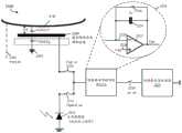
图1是具有包括指纹传感器181的指纹感应模块180的系统的示例的框图,该系统的实现可以包括基于本文件中所公开的指纹的光学感应的光学指纹传感器。系统180包括指纹传感器控制电路184和数字处理器186,该数字处理器186可以包括一个或多个处理器,用于处理指纹图案,并确定输入的指纹图案是否是授权用户的指纹图案。指纹感应系统180使用指纹传感器181来得到指纹并将得到的指纹与储存的指纹进行比较,以启用或禁用由指纹感应系统180保护的设备或系统188中的功能。操作中,指纹处理处理器186基于捕获的用户指纹是否来自授权用户,控制对设备188的访问。如图所示,指纹传感器181可以包括多个指纹感应像素,如统一表示指纹中的至少一部分的像素182A-182E。例如,指纹感应系统180可以在作为系统188的ATM处实现,以确定请求访问资金或其他交易的客户的指纹。基于对从指纹传感器181得到的用户的指纹与一个或多个储存的指纹的比较,响应于正面识别,指纹感应系统180可以使得ATM系统188准许请求的对用户账户的访问,或者响应于否定识别,可以拒绝访问。再如,设备或系统188可以是智能手机或便携式设备,并且指纹感应系统180是集成到设备188的模块。再如,设备或系统188可以是使用指纹传感器181来准许或拒绝进入的设施或家庭的门或安全入口。又如,设备或系统188可以是汽车或其他交通工具,其使用指纹传感器181链接到发动机的启动,并识别人是否被授权操作该汽车或交通工具。1 is a block diagram of an example of a system having a
作为具体的示例,图2A和2B示出了电子设备200的一个示例性实现,该电子设备200具有触摸感应显示屏幕组件和位于触摸感应显示屏幕组件下方的光学传感器模块。在该特定的示例中,显示技术可以通过具有发光显示像素而不使用背光的OLED显示屏幕或另一种显示屏幕来实现。电子设备200可以为智能手机或平板电脑等便携式设备,并且电子设备200可以为如图1所示的设备188。As a specific example, FIGS. 2A and 2B illustrate an exemplary implementation of an electronic device 200 having a touch-sensitive display screen assembly and an optical sensor module positioned below the touch-sensitive display screen assembly. In this particular example, the display technology may be implemented by an OLED display screen or another display screen with light-emitting display pixels without the use of a backlight. The electronic device 200 may be a portable device such as a smartphone or a tablet, and the electronic device 200 may be the
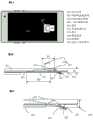
图2A示出了设备200的前侧,其类似于一些现有智能手机或平板电脑中的一些特征。设备屏幕在设备200的前侧,占据前侧空间的全部、大部分或显著部分,并且在设备屏幕上提供指纹感应功能,如用于在设备屏幕上接纳手指的一个或多个感应区域。作为示例,图2A示出了设备屏幕中用于手指触摸的指纹感应区,该指纹感应区可以被照亮为明显可识别的地区或区域,用户放置手指以进行指纹感应。这种指纹感应区可以像设备屏幕的其余部分一样用于显示图像。如图所示,在各种实现中,设备200的设备外壳可以具有侧面,该侧面支持当前市场上各种智能手机中常见的侧控制按钮。并且,如图2A中设备外壳的左上角的一个示例所示,在设备屏幕外的设备200的前侧上可以设置一个或多个可选的传感器。Figure 2A shows the front side of device 200, which is similar to some features in some existing smartphones or tablets. The device screen is on the front side of the device 200, occupies all, most or a significant portion of the front side space, and provides fingerprint sensing functions on the device screen, such as one or more sensing areas for receiving fingers on the device screen. As an example, FIG. 2A shows a fingerprint sensing area for finger touch in a device screen, which can be illuminated as a clearly recognizable area or area where a user places a finger for fingerprint sensing. This fingerprint sensing area can be used to display images like the rest of the device's screen. As shown, in various implementations, the device housing of device 200 may have sides that support side control buttons commonly found in various smartphones currently on the market. Also, as shown in one example in the upper left corner of the device housing in Figure 2A, one or more optional sensors may be provided on the front side of the device 200 outside the device screen.
图2B示出了设备200中与本文件中公开的光学指纹感应相关的模块的结构构造的示例。图2B中所示的设备屏幕组件包括:例如,在顶部具有触摸感应层的触摸感应屏幕模块、以及位于触摸感应模块下的具有显示层的显示屏幕模块。光学传感器模块耦合到显示屏幕组件模块并位于其下方,以接收和捕获来自触摸感应屏幕模块的顶面的返回的光,并且将该返回的光引导且成像到光学感应像素或光电探测器的光学传感器阵列上,该光学传感器阵列将该返回的光中的光学图像转换成像素信号以用于进一步处理。光学传感器模块之下是设备电子结构,该设备电子结构包含用于设备200中的光学传感器模块和其他部件的某些电子电路。该设备电子器件可以布置在设备外壳内部,并且可以包括如图2B所示的光学传感器模块的下面的一部分。FIG. 2B shows an example of the structural configuration of the modules in the device 200 related to the optical fingerprint sensing disclosed in this document. The device screen assembly shown in FIG. 2B includes, for example, a touch-sensitive screen module with a touch-sensitive layer on top, and a display screen module with a display layer below the touch-sensitive module. An optical sensor module is coupled to and positioned below the display screen assembly module to receive and capture returning light from the top surface of the touch-sensitive screen module, and to direct and image the returned light to optical sensing pixels or photodetectors On the sensor array, the optical sensor array converts the optical image in this returned light into pixel signals for further processing. Beneath the optical sensor module is the device electronics structure, which contains certain electronic circuits for the optical sensor module and other components in device 200 . The device electronics may be arranged inside the device housing and may include a lower portion of the optical sensor module as shown in Figure 2B.
在实现中,设备屏幕组件的顶面可以为光学透明层的表面,该光学透明层表面作为用户触摸感应表面以提供多种功能,例如(1)显示输出表面,携带显示图像的光穿过该显示输出表面到达观看者的眼睛,(2)触摸感应界面,接收用于触摸感应模块的触摸感应操作的用户触摸,以及(3)光学界面,用于屏幕上指纹感应(以及可能的一个或多个其他光学感应功能)。这种光学透明层可以为玻璃或晶体层或柔性层等刚性层。In implementations, the top surface of the device screen assembly may be the surface of an optically transparent layer that acts as a user touch-sensitive surface to provide multiple functions, such as (1) a display output surface through which light carrying a display image passes. The display output surface reaches the viewer's eye, (2) a touch-sensing interface that receives user touches for touch-sensing operation of the touch-sensing module, and (3) an optical interface that is used for on-screen fingerprint sensing (and possibly one or more other optical sensing functions). Such optically transparent layers may be rigid layers such as glass or crystalline layers or flexible layers.
具有发光显示像素而不使用背光的显示屏幕的一个示例是具有单独的发射像素的阵列以及薄膜晶体管(TFT)结构或基板的OLED显示器,其中,该薄膜晶体管结构或基板可以包括小孔阵列,并且可以是光学透明的,并且可以是覆盖基板以保护OLED像素。参见图2B,本示例中的光学传感器模块位于OLED显示面板的下面,以捕获来自该顶部触摸感应表面的返回的光,并且获取当用户的手指与该顶面上的感应区域接触时的指纹图案的高分辨率图像。在其他实现中,所公开的用于指纹感应的屏幕下光学传感器模块可以在没有触摸感应特征的设备上实现。此外,合适的显示面板可以有不同于OLED显示器的各种屏幕设计。An example of a display screen with emissive display pixels without the use of a backlight is an OLED display with an array of individual emissive pixels and a thin film transistor (TFT) structure or substrate, wherein the thin film transistor structure or substrate may include an array of pinholes, and Can be optically transparent and can be a cover substrate to protect the OLED pixels. Referring to FIG. 2B, the optical sensor module in this example is located under the OLED display panel to capture the returning light from the top touch-sensing surface and acquire the fingerprint pattern when the user's finger is in contact with the sensing area on the top surface high-resolution images. In other implementations, the disclosed under-screen optical sensor modules for fingerprint sensing may be implemented on devices without touch-sensing features. Furthermore, suitable display panels can have various screen designs other than OLED displays.
图2C和2D示出了实现图2A和2B中的光学传感器模块的设备的示例。图2C示出了包含屏幕下光学传感器模块的设备的一部分的横截面视图。图2D在左侧示出了具有触摸感应显示器的设备的前侧的视图,表示显示屏幕下部上的指纹感应区域,并且在右侧示出了包含位于设备显示屏幕组件下面的光学传感器模块的设备的一部分的透视图。图2D还示出了具有电路元件的柔性带的布局的示例。Figures 2C and 2D show examples of devices implementing the optical sensor module of Figures 2A and 2B. Figure 2C shows a cross-sectional view of a portion of a device containing an under-screen optical sensor module. Figure 2D shows a view of the front side of a device with a touch-sensitive display on the left, representing the fingerprint sensing area on the lower portion of the display screen, and on the right, a device containing an optical sensor module located under the device's display screen assembly Perspective view of part of. Figure 2D also shows an example of the layout of the flexible tape with circuit elements.
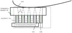
在图2A、2B、2C和2D的设计示例中,光学指纹传感器设计不同于一些其他的指纹传感器设计,这些设计使用独立于显示屏幕的指纹传感器结构,并且在移动设备的表面上,显示屏幕和指纹传感器之间具有物理分界(例如,一些移动电话设计中在顶部玻璃盖板的开口中的按钮状结构)。在本文所示的设计中,用于检测指纹感应和其他光学信号的光学指纹传感器位于顶部盖板玻璃或层的下面(例如图2C),使得盖板玻璃的顶面用作移动设备的顶面,作为横跨垂直堆叠并垂直重叠的显示屏幕层和光学检测器传感器的连续且均匀的玻璃表面。用于将光学指纹感应和对触摸灵敏的显示屏幕集成在共同且均匀的表面下的这种设计提供了益处,包括提高了设备一体化,增强了设备封装,增强了设备对外部元件、故障、磨损和撕裂的抵抗力,并且增强了设备的所有权期间的用户体验。In the design examples of Figures 2A, 2B, 2C, and 2D, the optical fingerprint sensor design differs from some other fingerprint sensor designs that use a fingerprint sensor structure independent of the display screen, and on the surface of the mobile device, the display screen and There is a physical demarcation between the fingerprint sensors (eg, a button-like structure in the opening of the top glass cover in some mobile phone designs). In the design shown here, the optical fingerprint sensor used to detect fingerprint sensing and other optical signals is located under the top cover glass or layer (eg, Figure 2C), so that the top surface of the cover glass acts as the top surface of the mobile device , as a continuous and uniform glass surface across the vertically stacked and vertically overlapping display screen layers and optical detector sensors. This design for integrating optical fingerprint sensing and a touch-sensitive display screen under a common and uniform surface provides benefits including improved device integration, enhanced device packaging, enhanced device immunity to external components, faults, Wear and tear resistance, and enhances the user experience during device ownership.
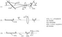
各种OLED显示设计和触摸感应设计可以用于图2A、2B、2C和2D中的光学传感器模块之上的设备屏幕组件。图3示出了OLED显示和触摸感应组件的一个示例,该示例是苹果公司的名称为“集成的硅-OLED显示和触摸传感器面板”、2015年11月19日公开的公开号为US2015/0331508A1的美国专利申请的图7B,该申请通过引用并入本专利文件的一部分。OLED可以以各种类型或配置来实现,包括但不限于无源矩阵OLED(PMOLED)、有源矩阵OLED(AMOLED)、透明OLED、阴极共用OLED、阳极共用OLED、白光OLED(WOLED)和三原色OLED。不同类型的OLED可以有不同的用途、配置和优点。在具有集成的硅-OLED显示和触摸传感器面板的系统的示例中,该系统可以包括硅基板、晶体管阵列、一个或多个金属化层、一个或多个通孔、OLED叠层、滤色器、触摸传感器以及附加的部件和电路。附加的部件和电路可以包括静电放电设备、光屏蔽、开关矩阵、一个或多个光电二极管、近红外检测器和近红外滤色器。集成的硅-OLED显示和触摸传感器面板还可以配置用于近场成像、光学辅助触摸和指纹检测。在一些示例中,多个触摸传感器和/或显示像素可以被分组成集群,并且该集群可以耦合到开关矩阵以用于触摸和/或显示粒度的动态变化。在图3的OLED示例和其他实现中,触摸传感器和触摸感应电路可以包括,例如,驱动线和感应线等触摸信号线、接地区域和其他电路。减少集成的触摸屏幕的尺寸的一种方式可以是包括多功能电路元件,该多功能电路元件可以形成设计为以显示系统的电路运行的显示线路的一部分,以在显示器上生成图像。该多功能电路元件还可以形成可以感应在显示器上或显示器附近的一个或多个触摸的触摸感应系统的触摸感应电路中的一部分。该多功能电路元件可以是,例如,LCD的显示像素中的电容器,该电容器可以用于以显示系统中显示电路的存储电容器/电极、公共电极、导线/路径等运行,并且还可以用于以触摸感应电路的电路元件运行。图3中OLED显示器示例可以实现为将多点触摸功能包括到OLED显示器,而不需要覆盖OLED显示器的分离的多点触摸面板或层。OLED显示器、显示电路、触摸传感器和触摸电路可以在硅基板上形成。通过在硅基板上制造集成的OLED显示器和触摸传感器面板,可以实现极高的每英寸像素(PPI)。针对OLED和触摸感应结构的不同于图3的其他布置也是可能的。例如,触摸感应层可以是位于OLED显示组件的顶部的组件。Various OLED display designs and touch-sensing designs can be used for the device screen assembly over the optical sensor modules in Figures 2A, 2B, 2C, and 2D. Figure 3 shows an example of an OLED display and touch sensing assembly, which is Apple's name "Integrated Silicon-OLED Display and Touch Sensor Panel", publication number US2015/0331508A1 published on November 19, 2015 7B of the US Patent Application, which is incorporated by reference in a part of this patent document. OLEDs can be implemented in various types or configurations, including but not limited to passive matrix OLEDs (PMOLEDs), active matrix OLEDs (AMOLEDs), transparent OLEDs, shared cathode OLEDs, shared anode OLEDs, white light OLEDs (WOLEDs), and trichromatic OLEDs . Different types of OLEDs can have different uses, configurations and advantages. In an example of a system with an integrated silicon-OLED display and touch sensor panel, the system may include a silicon substrate, a transistor array, one or more metallization layers, one or more vias, OLED stacks, color filters , touch sensors, and additional components and circuits. Additional components and circuits may include electrostatic discharge devices, light shields, switch matrices, one or more photodiodes, near-infrared detectors, and near-infrared color filters. The integrated silicon-OLED display and touch sensor panel can also be configured for near-field imaging, optically assisted touch and fingerprint detection. In some examples, multiple touch sensors and/or display pixels may be grouped into clusters, and the clusters may be coupled to a switch matrix for dynamic changes in touch and/or display granularity. In the OLED example of FIG. 3 and other implementations, the touch sensor and touch sensing circuitry may include, for example, touch signal lines such as drive and sense lines, ground regions, and other circuitry. One way to reduce the size of an integrated touch screen may be to include multifunctional circuit elements that may form part of a display circuit designed to operate with the circuitry of the display system to generate an image on the display. The multifunctional circuit element can also form part of a touch sensing circuit of a touch sensing system that can sense one or more touches on or near the display. The multifunctional circuit element can be, for example, a capacitor in a display pixel of an LCD that can be used to operate as a storage capacitor/electrode, common electrode, wire/path, etc. of a display circuit in a display system, and can also be used to The circuit elements of the touch sensing circuit operate. The OLED display example of Figure 3 can be implemented to incorporate multi-touch functionality into the OLED display without requiring a separate multi-touch panel or layer covering the OLED display. OLED displays, display circuits, touch sensors, and touch circuits can be formed on silicon substrates. Very high pixels per inch (PPI) can be achieved by fabricating an integrated OLED display and touch sensor panel on a silicon substrate. Other arrangements than Figure 3 are also possible for the OLED and touch-sensing structures. For example, the touch sensing layer may be an assembly on top of an OLED display assembly.
返回参考图2A和2B,所示的用于屏幕上指纹感应的屏幕下光学传感器模块可以以各种配置来实现。Referring back to Figures 2A and 2B, the illustrated under-screen optical sensor module for on-screen fingerprint sensing can be implemented in various configurations.
在一个实现中,基于上述设计的设备可以被构造为包括设备屏幕,该设备屏幕提供触摸感应操作并且包括具有发光显示像素的显示面板结构,每个像素可操作以发光,用于形成显示图像,该设备还包括顶部透明层,形成于设备屏幕之上,作为用于触摸感应操作的用户触摸界面并且作为用于传输来自显示面板结构的光以将图像显示给用户的界面,该设备还包括光学传感器模块,位于显示面板结构的下方,以接收由显示面板结构的发光显示像素中的至少一部分发出的并从顶部透明层返回的光来检测指纹。In one implementation, a device based on the above design may be constructed to include a device screen that provides touch-sensitive operation and includes a display panel structure having light-emitting display pixels, each pixel operable to emit light for forming a display image, The device also includes a top transparent layer formed over the device screen as a user touch interface for touch sensing operations and as an interface for transmitting light from the display panel structure to display images to the user, the device further includes optics A sensor module is positioned below the display panel structure to detect fingerprints by receiving light emitted by at least a portion of the light-emitting display pixels of the display panel structure and returned from the top transparent layer.
该设备还可以配置有各种特征。The device can also be configured with various features.
例如,设备电子控制模块可以包括在该设备中,以在检测到的指纹与授权用户的指纹匹配时授权用户对该设备的访问。此外,光学传感器模块除了用于检测指纹外,还用于通过光学感应检测不同于指纹的生物表征参数,以指示在顶部透明层处与检测到的指纹相关联的触摸是否来自活着的人,如果(1)检测到的指纹与授权用户的指纹匹配,并且(2)检测到的生物表征参数指示检测到的指纹来自活着的人,则设备电子控制模块用于授权用户对该设备的访问。该生物表征参数可以包括,例如,手指是否包含人的血流或心跳。For example, a device electronic control module may be included in the device to authorize user access to the device when a detected fingerprint matches that of an authorized user. In addition, the optical sensor module is used to detect biometric parameters other than fingerprints through optical sensing, in addition to the detection of fingerprints, to indicate whether the touch associated with the detected fingerprint at the top transparent layer is from a living person, if (1) The detected fingerprint matches the authorized user's fingerprint, and (2) the detected biometric parameter indicates that the detected fingerprint is from a living person, then the device electronic control module is used to authorize the user's access to the device. The biometric parameter may include, for example, whether the finger contains a person's blood flow or heartbeat.
例如,该设备可以包括耦合到显示面板结构的设备电子控制模块,以向发光显示像素提供电源,并控制显示面板结构的图像显示,以及在指纹感应操作中,设备电子控制模块操作关闭一帧中的发光显示像素并打开下一帧中的发光显示像素,以允许光学传感器阵列捕获具有发光显示像素照明和不具有发光显示像素照明的两个指纹图像,来减少指纹感应中背景光的影响。For example, the device may include a device electronic control module coupled to the display panel structure to provide power to the light emitting display pixels and to control the display of images on the display panel structure, and in fingerprint sensing operation, the device electronic control module operates off for a frame and turn on the illuminated display pixels in the next frame to allow the optical sensor array to capture both fingerprint images with and without illuminated display pixels to reduce the effects of background light in fingerprint sensing.
再如,设备电子控制模块可以耦合到显示面板结构,以向发光显示像素提供电源,并在睡眠模式下关闭发光显示像素的电源,并且当光学传感器模块在顶部透明层的指定的指纹感应区域处检测到人的皮肤的存在时,设备电子控制模块可以用于将显示面板结构从睡眠模式唤醒。更具体地,在一些实现中,当显示面板结构处于睡眠模式时,设备电子控制模块可以用于操作一个或多个选择的发光显示像素间歇性地发光,同时关闭其他发光显示像素的电源,将间歇发出的光指向顶部透明层的指定的指纹感应区域,以监控是否存在与指定的指纹感应区域接触的人的皮肤,用于将设备从睡眠模式唤醒。并且,显示面板结构可以被设计除了包括发光显示像素外,还包括一个或多个LED灯,以及当显示面板结构处于睡眠模式时,设备电子控制模块用于操作一个或多个LED灯间歇性地发光,同时关闭发光显示像素的电源,将间歇发出的光指向顶部透明层的指定的指纹感应区域,以监控是否存在与指定的指纹感应区域接触的、用于将设备从睡眠模式唤醒的人的皮肤。As another example, the device electronic control module can be coupled to the display panel structure to provide power to the light-emitting display pixels and power off the light-emitting display pixels in sleep mode, and when the optical sensor module is at the designated fingerprint sensing area of the top transparent layer When the presence of human skin is detected, the device electronic control module can be used to wake the display panel structure from sleep mode. More specifically, in some implementations, when the display panel configuration is in a sleep mode, the device electronic control module can be used to operate one or more selected light-emitting display pixels to emit light intermittently, while powering off other light-emitting display pixels, turning the Intermittent light is directed to the designated fingerprint sensing area of the top transparent layer to monitor the presence of human skin in contact with the designated fingerprint sensing area, used to wake the device from sleep mode. Also, the display panel structure may be designed to include one or more LED lights in addition to the light-emitting display pixels, and the device electronic control module for operating the one or more LED lights intermittently when the display panel structure is in a sleep mode Lights up while powering off the illuminated display pixels, directing intermittent light to the designated fingerprint sensing area of the top transparent layer to monitor the presence of a person in contact with the designated fingerprint sensing area used to wake the device from sleep mode skin.
再如,该设备可以包括设备电子控制模块,该设备电子控制模块耦合到光学传感器模块,以接收通过感应手指的触摸获得的多个检测到的指纹的信息,并且该设备电子控制模块被操作来测量该多个检测到的指纹的变化并确定造成测量到的该变化的触摸力。例如,该变化可以包括由于触摸力引起的指纹图像的变化、由于触摸力引起的触摸区域的变化或指纹脊的间距的变化。As another example, the device may include a device electronic control module coupled to the optical sensor module to receive information of a plurality of detected fingerprints obtained by sensing a touch of a finger, and the device electronic control module is operated to A change in the plurality of detected fingerprints is measured and the touch force causing the measured change is determined. For example, the change may include a change in the fingerprint image due to the touch force, a change in the touch area due to the touch force, or a change in the spacing of the fingerprint ridges.
再如,顶部透明层可以包括用于用户用手指触摸以进行指纹感应的指定的指纹感应区域,并且显示面板结构下方的光学传感器模块可以包括与显示面板基板接触的透明块,以接收从该显示面板结构发出的并从该顶部透明层返回的光,该光学传感器模块还可以包括接收该光的光学传感器阵列以及光学成像模块,该光学成像模块将该透明块中接收到的该光成像到该光学传感器阵列上。该光学传感器模块可以相对于指定的指纹感应区域设置,并且被构造成:当与人的皮肤接触时,在顶部透明层的顶面处通过全内反射选择性地接收返回的光,而在没有人的皮肤的接触时,不接收来自指定的指纹感应区域的返回的光。For another example, the top transparent layer may include a designated fingerprint sensing area for the user to touch with a finger for fingerprint sensing, and the optical sensor module under the display panel structure may include a transparent block in contact with the display panel substrate to receive the display from the display panel. the light emitted by the panel structure and returned from the top transparent layer, the optical sensor module may further include an optical sensor array that receives the light and an optical imaging module that images the light received in the transparent block to the on the optical sensor array. The optical sensor module may be positioned relative to a designated fingerprint sensing area, and is configured to selectively receive returned light by total internal reflection at the top surface of the top transparent layer when in contact with human skin, and to receive returned light at the top surface of the top transparent layer without When the human skin is in contact, it does not receive the returned light from the designated fingerprint sensing area.
又如,光学传感器模块可以被构造成包括位于显示面板结构下方的光楔,以修改与该光楔接合的显示面板结构的底面上的全反射条件,来允许从该显示面板结构提取出穿过该底面的光,该光学传感器模块还可以包括光学传感器阵列,接收来自该光楔的从该显示面板结构提取出的光,还可以包括光学成像模块,位于该光楔和该光学传感器阵列之间,以将来自该光楔的光成像到该光学传感器阵列上。As another example, an optical sensor module may be configured to include an optical wedge beneath a display panel structure to modify total reflection conditions on the bottom surface of the display panel structure to which the optical wedge engages to allow extraction of through-passage from the display panel structure For the light from the bottom surface, the optical sensor module may further include an optical sensor array for receiving the light extracted from the display panel structure from the optical wedge, and may also include an optical imaging module located between the optical wedge and the optical sensor array , to image the light from the wedge onto the optical sensor array.
下面提供了用于屏幕上指纹感应的屏幕下光学传感器模块的具体示例。Specific examples of under-screen optical sensor modules for on-screen fingerprint sensing are provided below.
图4包括图4A和图4B,并且示出了显示屏幕组件下面的光学传感器模块的一个实现的示例,该光学传感器模块用于实现图2A和图2B中的设计。图4中的设备包括具有顶部透明层431的显示组件423,该顶部透明层431形成于设备屏幕组件432之上,作为用于触摸感应操作的用户触摸界面并且作为用于传输来自显示面板结构的光以将图像显示给用户的界面。在一些实现中,该顶部透明层431可以是盖板玻璃或晶体材料。设备屏幕组件423可以包括顶部透明层431下面的OLED显示模块433。OLED显示模块433包括OLED层及其他,该OLED层包括发出用于显示图像的光的OLED像素阵列。OLED层具有光学地用作孔和光散物体的阵列的电极和布线结构。OLED层中的孔阵列允许来自顶部透明层431的光的传输通过该OLED层到达该OLED层下面的该光学传感器模块,并且由OLED层造成的光散射影响屏幕下光学传感器模块的用于指纹感应的光学检测。设备电路模块435可以设置在该OLED显示面板的下面,以控制该设备的操作,并且为用户执行功能以操作该设备。Figure 4 includes Figures 4A and 4B and shows an example of one implementation of an optical sensor module below the display screen assembly used to implement the designs in Figures 2A and 2B. The device in FIG. 4 includes a
本特定实现示例中的该光学传感器模块位于OLED显示模块433下。可以控制指纹照明区613中的OLED像素发光,以照亮设备屏幕区域内的顶部透明层431上的指纹感应区615,使用户将手指放入其中来进行指纹识别。如图所示,手指445被放置在照亮的指纹感应区615中,该指纹感应区615作为用于指纹感应的有效感应区。指纹照明区613中被OLED像素照亮的区615中的反射或散射的光中的一部分被指向OLED显示模块433下的光学传感器模块中,并且光学传感器模块内的光电探测器感应阵列接收这种光,并且捕获由接收的该光所携带的指纹图案信息。The optical sensor module in this particular implementation example is located under the
在这种设计中,使用OLED显示面板内的指纹照明区613中的OLED像素来为光学指纹感应提供照明光,可以控制指纹照明区613中的OLED像素以较低的周期间歇性地开启,以减少用于光学感应操作的光学功率。例如,当OLED面板中剩余的OLED像素被关闭(如处于睡眠模式)时,指纹照明区613中的OLED像素可以间歇性地开启,以发出用于光学感应操作的照明光,该光学感应操作包括执行光学指纹感应和唤醒OLED面板。在一些实现中,该指纹感应操作可以以两步骤的过程实现:首先,以闪光模式开启OLED显示面板内指纹照明区613中的数个OLED像素,而不开启该指纹照明区613中其他的OLED像素,以使用闪光来感应手指是否触摸感应区615,并且一旦检测到区615中的触摸,开启指纹照明区613中OLED像素,以激活光学感应模块进行指纹感应。并且,响应于激活该光学感应模块以进行指纹感应,指纹照明区613中的OLED像素可以在明亮水平下操作,以提高指纹感应的光学检测性能,例如,在比显示图像中的亮度水平更高的亮度水平下操作。In this design, the OLED pixels in the
在图4B的示例中,屏幕下光学传感器模块包括耦合到该显示面板的透明块701,该透明块701接收来自设备组件的顶面的返回的光,该返回的光最初是由指纹感应区613中的OLED像素发出的,该屏幕下光学传感器模块还包括执行光学成像和成像捕获的光学成像块702。来自指纹照明区613中的OLED像素的光在到达盖板顶表面后,例如,用户手指触摸的感应区域615处的盖板顶表面,从该盖板顶表面反射或散射回来。当感应区域615中的盖板顶表面紧密接触指纹脊时,由于在该位置处接触的手指的皮肤或组织的存在,指纹脊下的光反射不同于另一位置处的指纹谷下的光反射,该另一位置处的指纹谷下没有手指的皮肤或组织。该盖板顶表面上的手指触摸的区域中脊和谷的位置处的光反射条件的这种不同形成了图像,该图像表示该手指的被触摸部分的脊和谷的图像或空间分布。该反射光被指向返回OLED像素,并且在穿过OLED显示模块433的小孔后,到达该光学传感器模块的低指数光学透明块701的界面。该低指数光学透明块701的折射率被构造成小于OLED显示面板的折射率,使得可以将返回的光从OLED显示面板提取到该光学透明块701中。一旦该返回的光在该光学透明块701内被接收,这种接收到的光进入作为成像感应块702的一部分的光学成像单元,并且被成像到块702内的光电探测器感应阵列或光学感应整列上。指纹脊和谷之间的光反射差异造成了指纹图像的对比。图4B所示的是控制电路704(例如微控制器或MCU),其耦合到成像感应块702和主电路板上的设备主处理器705等其他电路。In the example of FIG. 4B , the under-screen optical sensor module includes a
在该特定的例子中,光学光路设计是:光线在基板和空气界面之间的顶面上的总反射角内进入盖板顶表面,并会被块702中的成像光学器件和成像传感器阵列最有效地收集。在这种设计中,指纹脊/谷区域的图像呈现最大的对比。这种成像系统可能具有会对指纹感应有不利影响的不期望的光学失真。因此,基于光学传感器阵列处的,沿返回光线的光路的光学失真情况,在处理块702中的光学传感器阵列的输出信号时,获取的图像还可以在成像重建期间通过失真校正来校正。通过在X方向线和Y方向线的整个感应区域,每次扫描一行像素的测试图像图案,失真校正系数可以由每个光电探测器像素处捕获的图案生成。这种校正过程还可以使用来自于每次调谐一个单独的像素且扫描光电探测器阵列的整个图像区域产生的图像。这种校正系数只需要在组装传感器之后生成一次。In this particular example, the optical path design is such that light rays enter the top surface of the cover plate within the total angle of reflection on the top surface between the substrate and air interface, and will be maximized by the imaging optics and imaging sensor array in
来自环境的背景光(如太阳光或室内光)可以通过OLED显示组件433中的TFT基板孔穿过OLED面板顶面进入图像传感器。这种背景光可以在来自手指的有价值的图像中产生背景基线,并且这种背景基线是不期望的。可以使用不同的方法来减少这种基线强度。一个示例是以一定的频率F调谐接通和断开指纹照明区613中的OLED像素,通过对像素驱动脉冲和图像传感器帧进行相位同步,图像传感器得以相同频率获取接收到的图像。在这种操作下,不同相位的图像中只有一个包含从OLED像素发射的光。通过减去奇数和偶数帧,可能得到大部分由指纹照明区613中调制的OLED像素发射的光所组成的图像。基于该设计,每个显示扫描帧生成指纹信号的帧。如果通过在一帧中谐调接通指纹照明区613中的OLED像素并在另一帧中调谐断开指纹照明区613中的OLED像素,去除两个连续的信号帧,则可以将环境的背景光影响最小化或大量消除。在实现中,指纹感应帧速率可以是显示帧速率的一半。Background light from the environment (eg, sunlight or room light) can enter the image sensor through the TFT substrate hole in the
来自指纹照明区613中OLED像素的光中的一部分还可以穿过盖板顶面,并进入手指组织。这部分的光功率被散在周围,并且该散射光中的一部分可以穿过OLED面板基板上的小孔,并最终被光学传感器模块中的成像传感器阵列收集。该散射光的光强度取决于手指的肤色和手指组织中的血液浓度,并且手指上的该散射光携带的这种信息对指纹感应是有用的,并且可以作为指纹感应操作的一部分被检测。例如,通过集成用户手指图像的区域的强度,可能会观察到,血液浓度的增加/减少取决于用户心跳的相位。这种特征可以用于确定用户的心跳速率,确定用户的手指是活体手指,还是具备伪造的指纹图案的欺骗设备。A portion of the light from the OLED pixels in the
返回至图3中的OLED显示器示例,OLED显示器通常具有不同的颜色像素,如相邻的红色、绿色和蓝色像素形成一个彩色OLED像素。通过控制开启每个彩色像素内的哪种颜色的像素并记录相应的测量强度,可以确定用户的肤色。例如,当用户注册了用于指纹认证操作的手指时,光学指纹传感器还测量来自手指的颜色A和B的散射光的强度,作为强度Ia和Ib。可以记录Ia/Ib的比率,以与当用户的手指放在感应区域上时测量指纹的晚些的测量结果作比较。该方法可以帮助拒绝可能与用户肤色不匹配的欺骗设备。Returning to the OLED display example in Figure 3, OLED displays typically have pixels of different colors, such as adjacent red, green, and blue pixels forming one color OLED pixel. By controlling which color pixel within each color pixel is turned on and recording the corresponding measured intensities, the user's skin tone can be determined. For example, when a user registers a finger for a fingerprint authentication operation, the optical fingerprint sensor also measures the intensities of scattered light of colors A and B from the finger as intensities Ia and Ib. The Ia/Ib ratio can be recorded for comparison with later measurements of the fingerprint when the user's finger is placed on the sensing area. This method can help reject spoofed devices that may not match the user's skin tone.
在一些实现中,为了在OLED显示面板为不开启时使用上述光学传感器模块提供指纹感应操作,如图4所示,可以将为提供指纹感应照明指定的一个或多个额外的LED灯源703设置在透明块701的侧面上。这种指定的LED灯703可以由用于控制块702中的图像传感器阵列的相同的电子器件704(如MCU)控制。该指定的LED灯703可以以低的占空比短时间地脉冲,以间歇性地发光并提供用于图像感应的脉冲光。图像传感器阵列可以被操作为以相同的脉冲占空比监控从OLED面板盖板基板反射的光图案。如果存在触摸屏幕上的感应区域615的人类手指,则在块702中的成像感应阵列处捕获的图像可以用于检测触摸事件。连接到块702中的图像传感器阵列的控制电子器件或MCU 704可以被操作为确定该触摸是否为人类手指触摸。如果确定是人类手指触摸事件,MCU704可以被操作为唤醒智能手机系统,开启OLED显示面板(或至少关闭指纹照明区613中的用于光学指纹感应的OLED像素),并使用正常模式获取完整的指纹图像。块702中的图像传感器阵列会向智能手机主处理器705发送获取的该指纹图像,该智能手机主处理器705可以被操作为将捕获的该指纹图像与注册的指纹数据库进行匹配。如果存在匹配的,智能手机会解锁手机,并启动正常操作。如果获取的该图像没有被匹配到,智能手机会向用户反馈该认证失败。用户可以再次尝试,或输入密码。In some implementations, in order to provide fingerprint sensing operation using the above-described optical sensor module when the OLED display panel is not turned on, as shown in FIG. 4, one or more additional LED
在图4(尤其是图4B)的示例中,屏幕下光学传感器模块使用光学透明块701和具有光电探测器感应阵列的成像感应块702,将与显示屏幕的顶面接触的触摸手指的指纹图案光学地成像在光电探测器感应阵列上。图4B中示出了从感应区615至块702中光电探测器阵列的光学成像轴或检测轴625。光学透明块701和光电探测器感应阵列之前的成像感应块702的前端形成了体成像模块,以实现用于光学指纹感应的合适的成像。由于该成像过程中的光学失真,如上所释,失真校正可以用于实现期望的成像操作。In the example of FIG. 4 (especially FIG. 4B ), the under-screen optical sensor module uses an optically
在本文公开的由图4中的屏幕下光学传感器模块和其他设计进行的光学感应中,从顶部透明层431上的感应区615到屏幕下光学传感器模块的光学信号包括不同的光组分。图5A和5B示出了用于两种不同的光学条件下从感应区615返回的光的信号生成,以便于理解屏幕下光学传感器模块的操作。In the optical sensing by the under-screen optical sensor module in FIG. 4 and other designs disclosed herein, the optical signal from the
图5A示出了来自OLED显示模块433的OLED发射的光如何在穿过顶部透明层431后生成到屏幕下光学传感器模块的不同的返回的光信号,该返回的光信号包括携带指纹图案信息的光信号。示出了两个不同位置处的两个OLED像素71和73,以发射OLED输出光束80和82,该OLED输出光束80和82被指向顶部透明层431,而在顶部透明层431的界面处不经历全反射。手指60与顶部透明层431上的感应区615接触。如图所示,OLED光束80在穿过顶部透明层431后,到达与顶部透明层431接触的手指脊,以在手指组织中生成光束183和向OLED显示模块433返回的另一光束181。OLED光束82在穿过顶部透明层431后,到达位于顶部透明层上方的手指谷,以生成从顶部透明层431的界面向OLED显示模块433返回的光束、进入手指组织的第二光束189以及由该手指谷反射的第三光束187。Figure 5A shows how the light emitted from the OLEDs of the
在图5A的示例中,假设手指皮肤在550nm处的等效折射率约为1.44,并且顶部透明层431的盖板玻璃折射率约为1.51。在这些假设下,在手指皮肤脊位置61处开启显示OLED像素71以产生光束80。手指脊-盖板玻璃的界面反射光束80的部分光,作为到OLED显示模块433下的底层524的反射的光181。其反射率低,约为0.1%。光束80中的大部分光变为传输至手指组织60中的光束183,手指组织60造成光183的散射,产生向OLED显示模块433和底层524返回的散射光191。来自OLED像素73的透射光束189在手指组织中的散射也对返回的散射光191有贡献。In the example of FIG. 5A , it is assumed that the equivalent refractive index of the finger skin at 550 nm is about 1.44, and the refractive index of the cover glass of the top
对于来自显示OLED组73的手指皮肤谷位置63处的光束82,盖板玻璃表面将入射光82功率的约3.5%(光185)反射到底层524,并且手指谷表面将该入射光功率的3.3%(光187)反射至底层524。总反射率约为6.8%。大部分光189被传输至手指组织60中。手指组织中的透射光189中的光功率中的一部分被手指组织散射,贡献到朝向并进入底层524中的散射光191中。For
因此,来自在触摸手指的手指谷和手指脊处的各种界面或表面的光反射是不同的,反射比差携带指纹地图信息,并且可以测量该反射比差以提取与顶部透明层431接触且被OLED光照射到的部分的指纹图案。Therefore, the light reflection from various interfaces or surfaces at the finger valleys and finger ridges of the touching finger is different, the reflectance difference carries the fingerprint map information, and this reflectance difference can be measured to extract the contact with the top
图5B示出了来自OLED显示模块433的OLED发射的光在与顶部透明层431的界面处的全反射条件下,如何生成到屏幕下光学传感器模块的不同的返回的光信号,该返回的光信号包括携带指纹图案信息的光信号。假设盖板玻璃431和OLED显示模块433被粘合在一起,两者之间没有任何气隙,使得由OLED像素73发出的、对盖板玻璃431具有大的入射角的OLED光束,会在盖板玻璃-空气界面处被全反射。当显示OLED像素73被开启时,发散光束可以被分成以下三组:(1)中心光束82,对盖板玻璃431具有小的入射角且没有全反射,(2)高对比度光束201、202、211和212,当盖板玻璃表面没有被触摸时,在盖板玻璃431处被全反射,并且当手指触摸盖板玻璃431时,可以耦合到手指组织中,以及(3)具有很大入射角的逃离光束,即使在手指组织触摸的位置处,也在盖板玻璃431处被全反射。5B shows how the light emitted from the OLED of the
对于中心光束82,盖板玻璃表面对着光束185反射约为0.1%~3.5%的光,这部分光被传输到底层524中,手指皮肤对光束187反射约为0.1%~3.3%的光,这部分光也被传输到底层524中。反射差取决于光束82是否与手指皮肤脊61或谷63相遇。剩余的光束189被耦合到指组织60中。For the
对于高对比度光束201和202,如果盖板玻璃表面没有被触摸,盖板玻璃表面分别对光束205和206反射几乎100%的光。当手指皮肤脊在光束201和202的位置处触摸盖板玻璃表面时,光功率中的大部分通过光束203和204耦合到手指组织60中。For high contrast beams 201 and 202, if the cover glass surface is not touched, the cover glass surface reflects almost 100% of the light for
对于高对比度光束211和212,如果盖板玻璃表面没有被触摸,盖板玻璃表面分别对光束213和214反射几乎100%的光。当手指触摸盖板玻璃表面且手指皮肤谷恰好处于光束211和212的位置时,没有光功率耦合到手指组织60中。For high contrast beams 211 and 212, if the cover glass surface is not touched, the cover glass surface reflects almost 100% of the light for
与图5A中的情况相似,耦合到手指组织60中的光束会经历手指组织的随机散射,以形成低对比度光191。Similar to the situation in FIG. 5A , the light beam coupled into
因此,在高对比光束照射的区域中,手指皮肤脊和谷引起不同的光学反射,并且反射差异图案携带指纹图案信息。高对比指纹信号可以通过比较这种差异来实现。Therefore, in the area illuminated by the high-contrast beam, the finger skin ridges and valleys cause different optical reflections, and the reflection difference pattern carries the fingerprint pattern information. High contrast fingerprint signals can be achieved by comparing this difference.
基于图2A和2B中的设计,所公开的屏幕下光学感应技术可以以各种配置来光学地捕获指纹。Based on the designs in Figures 2A and 2B, the disclosed under-screen optical sensing technology can optically capture fingerprints in various configurations.
例如,可以以各种配置来实现图4B中的具体实现,该实现是基于通过使用光学感应模块中的大块成像模块的光学成像。图6、7、8、9、10、11和12示出了用于光学指纹感应的屏幕下光学传感器模块设计的各种实现、附加特征和操作的示例。For example, the specific implementation in Figure 4B, which is based on optical imaging through the use of a bulk imaging module in an optical sensing module, can be implemented in various configurations. Figures 6, 7, 8, 9, 10, 11, and 12 illustrate examples of various implementations, additional features, and operations of an under-screen optical sensor module design for optical fingerprint sensing.
图6包括图6A、6B和6C,示出了基于通过透镜进行光学成像的屏幕下光学传感器模块的示例,用于从按压显示盖板玻璃423的手指445捕获指纹。图6C是图6B所示的光学传感器模块部分的放大视图。如图6B所示的屏幕下光学传感器模块位于OLED显示模块433下,该屏幕下光学传感器模块包括与OLED显示模块433的底面接触的光学透明垫片617,以接收来自顶部透明层上431的顶面上的感应区615返回的光,该屏幕下光学传感器模块还包括位于垫片617和光电探测器阵列623之间的成像透镜621,成像透镜621将接收到的来自感应区615的返回的光成像在光电探测器阵列623上。类似于图4B示例中的成像系统,图6B中用于光学传感器模块的成像系统可能经历图像失真,并且可以使用合适的光学校正校准来减少这种失真,例如,对图4B中系统所描述的失真校正方法。FIG. 6 , which includes FIGS. 6A , 6B, and 6C, shows an example of an under-screen optical sensor module based on optical imaging through a lens for capturing a fingerprint from a
与图5A和5B中的假设相似,假设手指皮肤在550nm处的等效折射率约为1.44,并且对于盖板玻璃423,裸的盖板玻璃的折射率约为1.51。当OLED显示模块433粘合在盖板玻璃431上且没有任何气隙时,全内反射在等于或大于界面的临界入射角的大角度发生。如果盖板玻璃顶面没有被接触,则全反射入射角约为41.8°,并且如果手指皮肤触摸盖板玻璃顶面,则全反射角约为73.7°。对应的全反射角差约为31.9°。Similar to the assumptions in Figures 5A and 5B, it is assumed that the equivalent refractive index of the finger skin at 550 nm is about 1.44, and for
在这种设计中,微透镜621和光电二极管阵列623限定了捕获感应区615中接触手指的图像的视角θ。为了检测感应区615中盖板玻璃表面中的期望的部分,可以通过控制物理参数或配置来适当地对准该视角。例如,可以对准视角以检测OLED显示组件的全内反射。具体地,对准观看视角θ来感应盖板玻璃表面上的有效感应区615。有效的感应盖板玻璃表面615可以被视为镜子,使得光电探测器阵列有效地检测视区或OLED显示中指纹照明区613的,由感应盖板玻璃表面615投射到光电探测器阵列上的图像。如果开启视区/指纹照明区613中的OLED像素来发光,光电二极管/光电探测器阵列623可以接收由感应盖板玻璃表面615反射的区613的图像。当手指触摸感应区615时,光中的一部分可以耦合到指纹的脊中,这会引起光电探测器阵列接收来自脊位置的光,以呈现为更暗的指纹图像。由于光学的检测路径的几何形状是已知的,所以可以校正在光学传感器模块中的光学路径中引起的指纹图像失真。In this design, the
作为具体的示例,考虑到图6B中从检测模块中心轴到盖板玻璃顶面的距离H为2mm,这种设计可以直接覆盖5mm的有效感应区615,该有效感应区615在盖板玻璃上具有宽度Wc。调整垫片617的厚度可以调整检测器位置参数H,并且可以优化有效感应区宽度Wc。由于H包括盖板玻璃431和显示模块433的厚度,所以该申请设计应当考虑这些层。垫片617、微透镜621和光电二极管阵列623可以集成在顶部透明层431的底面上的彩色涂层619的下方。As a specific example, considering that the distance H from the central axis of the detection module to the top surface of the cover glass in FIG. 6B is 2 mm, this design can directly cover the
图7示出了用于图6中示出的光学传感器模块的光学成像设计的另一设计考虑的示例,通过使用特殊的垫片618代替的图6中的垫片617,以增加感应区域615的尺寸。垫片618被设计为具有宽度Ws,厚度为Hs,具有低折射率(RI)ns,并且,垫片618位于OLED显示模块433下,例如,被附接(如粘合)到OLED显示模块433的底面。垫片618的端面是与微透镜621接合的成角度的或倾斜的面。垫片和透镜的这种相对位置不同于图6中透镜位于垫片617的下方。微透镜621和光电二极管阵列623被组装到具有检测角度大小为θ的光学检测模块中。由于在垫片618和显示模块433之间的界面处的光学折射以及在盖板玻璃431和空气之间的界面处的光学折射,检测轴625弯曲。局部入射角

如果nc大于ns,则


当特殊垫片618的折射率设计为足够低(如,使用MgF2、CaF2或甚至空气来形成垫片)时,有效感应区域615的宽度Wc不再受限于盖板玻璃431和显示模块433的厚度。这种性质使设计者具有想要的灵活性。原则上,如果检测模块具有足够的分辨率,甚至可以将有效感应区域到覆盖所有的显示屏幕。When the refractive index of the
因为所公开的光学传感器技术可以用于提供大的感应区域来捕获图案,所以所公开的屏幕下光学传感器模块不仅可以用于捕获和检测手指的图案,还可以用于捕获和检测更大尺寸的图案,例如与人相关联的人的手掌,来进行用户认证。Because the disclosed optical sensor technology can be used to provide a large sensing area to capture patterns, the disclosed under-screen optical sensor module can be used not only to capture and detect patterns of fingers, but also to capture and detect larger size Patterns, such as a person's palm associated with the person, for user authentication.
图8示出了用于图7中示出的光学传感器模块的光学成像设计的另一设计的示例,在该设计中,设置光电探测器阵列在显示屏幕表面中相对的检测角θ′以及透镜621和垫片618之间的距离L。图8A示出了沿着垂直于显示屏幕表面的方向的横截面视图,图8B示出了从显示屏幕底部或顶部看到的设备的视图。填充材料618c可以用于填充透镜621和光电探测器阵列623之间的间隔。例如,填充材料618c可以是与特殊垫片618相同的材料或者是另一种不同的材料。在一些设计中,填充材料618c可以是空气间隔。FIG. 8 shows an example of another design for the optical imaging design of the optical sensor module shown in FIG. 7 in which the relative detection angle θ′ of the photodetector array in the display screen surface and the lens are set Distance L between 621 and
图9示出了基于图7的设计中的屏幕下光学传感器模块的另一示例,其中OLED显示模块433中的视区或指纹照明区613设计为包括一个或多个额外的光源614,该额外的光源附着或粘合于与视区613相同的位置或区域中,以对感应区615提供附加的照明,从而增加了光学感应操作中的光强度。这是用来提高光学感应灵敏度的方法之一。额外的光源614可以是扩展类型或是准直类型的光源,以使得有效感应区615内所有的点被照亮。额外的光源614可以是单元件光源或光源阵列。如上所述,OLED显示模块433中的视区或指纹照明区613中的OLED像素可以在光学指纹感应操作期间操作于比用于在OLED显示器中显示图像的亮度水平更高的亮度水平。FIG. 9 shows another example of an under-screen optical sensor module in the design based on FIG. 7, wherein the viewing area or
图10示出了使用形状为薄楔的光学耦合器628的屏幕下光学传感器模块的示例,以提高在光学传感器阵列623处的光学检测。图10的图10A示出了具有用于指纹感应的屏幕下光学传感器模块的设备结构的横截面,图10B示出了设备屏幕的顶视图。光楔628(具有折射率ns)位于显示面板结构的下方,以修改与光楔628接合的显示面板结构的底面上的全反射条件,来允许从显示面板结构提取出穿过底面的光。光学传感器阵列623接收来自光楔628的从显示面板结构提取出的光,光学成像模块621位于光楔628和光学传感器阵列623之间,以将来自光楔628的光成像到光学传感器阵列623上。在所示的示例中,光楔628包括面对着光学成像模块和光学感应阵列623的倾斜光楔面。并且,如图所示,在光楔628和光学成像模块621之间存在自由间隔。FIG. 10 shows an example of an under-screen optical sensor module using an
如果光在盖板玻璃431的感应表面处被全反射,则反射率为100%,具有最高的效率。然而,如果光与盖板玻璃表面平行,则光还会在OLED底面433b处被全反射。楔形耦合器628用于修改局部表面角,以使得光可以耦合输出以用于在光学传感器阵列623处的检测。OLED显示模块431的TFT层中的微孔提供使得光穿过OLED显示模块431以进行屏幕下光学感应的期望的光传播路径。如果光透射角变得太大或当TFT层变得太厚时,实际的光透射效率可能逐渐减少。当该角度接近于全反射角时,即约为41.8°,且盖板玻璃折射率为1.5时,指纹图像看起来是好的。因此,楔形耦合器628的楔角可以被调整为数度,以使得检测效率可以提高或优化。如果选择更高的盖板玻璃的折射率,则全反射角变小。例如,如果盖板玻璃由折射率约为1.76的蓝宝石制成,则全反射角约为34.62°。显示器中的检测光透射效率也提高了。因此,这种设计使用薄楔将检测角设置为高于全反射角,和/或使用高折射率的盖板玻璃材料,来提高检测效率。If the light is totally reflected at the sensing surface of the
在图6至10中的屏幕下光学传感器模块中,顶部透明表面上的感应区域615不是竖直的或者不垂直于光学传感器模块的检测轴625,使得感应区域的图像平面也不是竖直的或不垂直于检测轴625。因此,光电探测器阵列523的平面相对于检测轴625可以是倾斜的,以实现在光检测阵列623处的高质量成像。In the under-screen optical sensor modules in Figures 6 to 10, the
图11示出了这种倾斜的三个示例配置。图11(1)示出了感应区域615a倾斜且不垂直于检测轴625。在(2)中所示的特定情况下,感应区域615b对准在检测轴625上,其图像平面也会位于检测轴625上。实践中,可以部分地切掉透镜621以简化封装。在各种实现中,微透镜621也可以是透射型或反射型透镜。例如,(3)中示出了特定的途径。感应区域615c由成像镜621a成像。光电二极管阵列623b对齐以检测信号。Figure 11 shows three example configurations of this tilt. FIG. 11(1) shows that the
在使用透镜621的上述设计中,透镜621的有效孔径可以被设计为大于OLED显示层中的孔的孔径,后者允许光透射穿过OLED显示器来进行光学指纹感应。这种设计可以减少OLED显示模块中的布线结构和其他散射物体的所造成不期望的影响。In the above designs using the
在所公开的指纹技术的一些实现中,光学传感器阵列623处的指纹感应对比度可以通过控制显示屏幕的OLED像素(613)来提高,该OLED像素在指纹触摸感应中提供用于捕获指纹图案的照明。当指纹传感器被激活时,例如,由于触摸的存在,局部视区613中的OLED像素可以被开启且具有高亮度,以提高指纹感应对比度。例如,局部视区613中的OLED像素的亮度可以被控制为高于当该局部视区613中相同的OLED像素用作常规显示时的最大亮度。In some implementations of the disclosed fingerprint technology, fingerprint sensing contrast at the
图12示出了指纹传感器的用于在指纹感应中减少或消除来自背景光的影响的操作的示例。光学传感器阵列可以用于捕获各种帧,并且捕获到的帧可以用于进行多个帧之间的差分和平均操作,以减少背景光的影响。例如,在帧A中,OLED显示器被开启,以照亮手指触摸的区域,在帧B中,改变或关闭OLED显示器的照明。从帧A的信号减去帧B的信号可以使用在图像处理中,以减少不期望的背景光影响。Figure 12 shows an example of the operation of the fingerprint sensor to reduce or eliminate the effects from background light in fingerprint sensing. An array of optical sensors can be used to capture various frames, and the captured frames can be used to perform differentiating and averaging operations between multiple frames to reduce the effects of background light. For example, in frame A, the OLED display is turned on to illuminate the area touched by the finger, and in frame B, the illumination of the OLED display is changed or turned off. Subtracting the signal of frame B from the signal of frame A can be used in image processing to reduce unwanted background light effects.
还可以通过在光路中提供合适的光学过滤来减少指纹感应中的不期望的背景光。一个或多个光学过滤器可以用于过滤掉环境光波长,例如,近红外光和部分的红光等。在一些实现中,这种光学过滤涂层可以制作在光学部件的表面上,包括显示器底面、棱镜表面或传感器表面等。例如,人类手指吸收波长低于~580nm的光的能量中的大部分,如果一个或多个光学过滤器或光学过滤涂层可以设计为过滤波长从580nm至红外的光,则可以大大减少环境光对指纹感应中的光学检测的影响。Undesirable background light in fingerprint sensing can also be reduced by providing suitable optical filtering in the light path. One or more optical filters may be used to filter out ambient light wavelengths, eg, near-infrared light, some red light, and the like. In some implementations, such optical filter coatings can be fabricated on surfaces of optical components, including display bottom surfaces, prism surfaces, or sensor surfaces, among others. For example, human fingers absorb most of the energy of light with wavelengths below ~580nm, and ambient light can be greatly reduced if one or more optical filters or optical filter coatings can be designed to filter light with wavelengths from 580nm to the infrared Impact on optical detection in fingerprint sensing.
图13示出了用于校正光学传感器模块中的图像失真的操作过程的示例。在步骤1301处,某些显示像素被控制和操作于在特定区域中发光,并且这种像素的光发射由频率F调制。在步骤1302处,显示面板下的成像传感器的帧速率被操作为和频率F相同,以捕获图像。在光学指纹感应操作中,手指放置在显示面板盖板基板的顶部上,并且手指的存在调制该显示面板盖板基板顶面的光反射强度。该显示器下的成像传感器捕获指纹调制的反射光图案。在步骤1303处,对来自图像传感器的信号的解调制以频率F同步,并且进行背景过滤。所得的图像减少了背景光的影响,并且包括来自像素发射的光产生的图像。在步骤1304处,处理并校准捕获到的图像,以校正图像系统失真。在步骤1305处,将校正了的图像用作用于用户认证的人类指纹图像。FIG. 13 shows an example of an operational procedure for correcting image distortion in an optical sensor module. At
用于捕获用户的指纹而使用的相同的光学传感器还可以用于捕获来自被照亮手指的散射光,如图5A和5B中的散射到底层中的光191所示。可以集成来自图5A和5B中的散射到底层中的光191的感兴趣区域中的检测器信号,以产生强度信号。评估该强度信号的强度变化以确定用户的心率。The same optical sensor used to capture the user's fingerprint can also be used to capture scattered light from the illuminated finger, as shown by scattered light 191 into the bottom layer in Figures 5A and 5B. The detector signal in the region of interest from the light 191 scattered into the bottom layer in Figures 5A and 5B can be integrated to generate an intensity signal. The change in intensity of this intensity signal is evaluated to determine the user's heart rate.
上述指纹传感器可以被能够得到授权用户的指纹并且将被偷盗的指纹图案复制在类似于人类手指的载体上的恶意的个体黑客攻击。这种未授权的指纹图案可以用在指纹传感器上,以解锁目标设备。因此,指纹图案,尽管是唯一的生物表征标识符,其本身可能不是完全可靠或安全的标识。屏幕下光学传感器模块还可以用作光学反欺骗传感器,用于感应具有指纹图案的输入物体是否是来自活着的人的手指,并且用于确定指纹输入是否为指纹欺骗攻击。无需使用单独的光学传感器来提供这种光学反欺骗感应功能。光学反欺骗能够提供高速响应,而不损害指纹感应操作的整体响应速度。The above fingerprint sensor can be hacked by malicious individuals who can obtain the fingerprint of an authorized user and reproduce the stolen fingerprint pattern on a carrier similar to a human finger. This unauthorized fingerprint pattern can be used on the fingerprint sensor to unlock the target device. Therefore, a fingerprint pattern, although a unique biometric identifier, may not by itself be a completely reliable or secure identification. The under-screen optical sensor module can also be used as an optical anti-spoofing sensor for sensing whether an input object with a fingerprint pattern is a finger from a living person, and for determining whether the fingerprint input is a fingerprint spoofing attack. There is no need to use a separate optical sensor to provide this optical anti-spoofing sensing capability. Optical anti-spoofing provides high-speed response without compromising the overall responsiveness of fingerprint sensing operations.
图14A示出了在血液中监控的材料的示例性消光系数,血液中的光学吸收在如660nm的红光的可见光谱范围和如940nm的红外光的红外范围之间是不同的。通过使用探测光以在第一可视波长(颜色A)和红外波长(颜色B)等第二不同波长来照亮手指,可以捕获输入物体的光学吸收的不同,以确定触摸的物体是否为来自活着的人的手指。因为OLED像素包括发出不同颜色的光的OLED像素,发出至少两种不同的光学波长的探测光,以使用血液的不同光学吸收行为来进行活体手指检测。当人的心脏跳动时,脉搏压力泵送血液在动脉中流动,因此在血液中监控的材料的消光比随着脉搏而变化。接收到的信号携带脉搏信号。血液的这些性质可以用于检测被监控的材料是活体指纹还是假指纹。Figure 14A shows exemplary extinction coefficients of materials monitored in blood, where the optical absorption differs between the visible spectral range of red light, such as 660 nm, and the infrared range of infrared light, such as 940 nm. By using probe light to illuminate the finger at a second different wavelength, such as a first visible wavelength (color A) and an infrared wavelength (color B), the difference in optical absorption of the input object can be captured to determine whether the touched object is from Fingers of the living man. Because OLED pixels include OLED pixels that emit light of different colors, at least two different optical wavelengths of probe light are emitted to use the different optical absorption behavior of blood for live finger detection. When a person's heart beats, the pulse pressure pumps blood through the arteries, so the extinction ratio of the material monitored in the blood changes with the pulse. The received signal carries the pulse signal. These properties of blood can be used to detect whether the material being monitored is a live fingerprint or a fake fingerprint.
图14B示出了来自无生命材料(如假手指)和活体手指的反射光中的光学信号行为之间的比较。光学指纹传感器也可以用作心跳传感器运行,来监控活着的生物。当检测到探测光的两个或多个波长时,消光比差可以用于快速地确定被监控的材料是否是活着的生物,例如活体指纹。在图14B所示的示例中,使用了不同波长的探测光,如图14A所示,一个是可视波长,另一个为红外波长。Figure 14B shows a comparison between optical signal behavior in reflected light from inanimate material (eg, a fake finger) and a living finger. Optical fingerprint sensors can also function as heartbeat sensors to monitor living creatures. When two or more wavelengths of probe light are detected, the difference in extinction ratio can be used to quickly determine whether the material being monitored is a living organism, such as a living fingerprint. In the example shown in Fig. 14B, different wavelengths of probe light are used, as shown in Fig. 14A, one is a visible wavelength and the other is an infrared wavelength.
当无生命材料触摸指纹传感器模块上方的顶部盖板玻璃时,接收到的信号揭示了与该无生命材料的表面图案相关的强度水平,并且该接收到的信号不包含与活着的人的手指相关联的信号分量。然而,当活着的人的手指触摸顶部盖板玻璃时,该接收到的信号揭示了与活着的人相关联的信号特征,由于不同波长的消光比不同,所以该接收到的信号包括明显不同的强度水平。这种方法不需要花很长时间来确定触摸材料是否是活着的人的一部分。图14B中,脉冲状信号反应了多次触摸的情形,而不是血液脉冲。无生命材料的相似的多次触摸不显示由活体手指引起的差异。When the inanimate material touches the top cover glass above the fingerprint sensor module, the received signal reveals an intensity level associated with the surface pattern of the inanimate material, and the received signal does not contain associations with a living human finger connected signal components. However, when a living person's finger touches the top cover glass, the received signal reveals signal characteristics associated with a living person, including significantly different extinction ratios for different wavelengths intensity level. This method doesn't take long to determine if the touching material is part of a living person. In Figure 14B, the pulse-like signal reflects multiple touch conditions, rather than blood pulses. Similar multiple touches of inanimate material did not show differences caused by living fingers.
血液在不同光学波长处的不同光学吸收行为的这种光学感应可以在短周期内进行,以用于活体手指检测,并且可以比使用相同光学传感器的人的心跳的光学检测更快。This optical sensing of the different optical absorption behavior of blood at different optical wavelengths can be performed in short periods for in vivo finger detection, and can be faster than the optical detection of a human heartbeat using the same optical sensor.
图15示出了通过操作OLED像素以用两种不同颜色的光照亮手指来确定与OLED显示屏幕接触的物体是否是活着的人的手指的一部分的操作过程的示例。FIG. 15 shows an example of an operation process for determining whether an object in contact with an OLED display screen is part of a living person's finger by manipulating OLED pixels to illuminate the finger with two different colors of light.
又如,所公开的光学传感器技术可以用于通过除上述血液在不同光学波长处的不同光学吸收之外的其他机制,通过“活体手指”检测机制检测捕获到的或检测到的指纹或手掌的图案是否来自活着的人的手。例如,由于人的自然移动或运动(有意或无意地)或当血液流过人体时的与心跳相关的脉搏,活着的人的手指通常是移动着或伸展着的。在一个实现中,光学传感器模块可以检测来自手指或手掌的返回的光的由于心跳/血流变化而导致的变化,从而检测在表现为手指或手掌的物体中是否存在活着的心跳。用户认证可以基于指纹/手掌图案的光学感应和对存在活着的人的正面确定的结合来增强访问控制。作为另一个例子,当人触摸OLED显示屏幕时,触摸力的变化可以以一种或多种方式反映,包括指纹图案变形,手指和屏幕表面之间的接触区域的变化,指纹脊变宽,或血流的动态变化。这些或其他变化可以通过基于所公开的光学传感器技术的光学感应来测量,并且可以用于计算触摸力。这种触摸力感应可以用于为光学传感器模块添加除指纹感应之外的更多的功能。As another example, the disclosed optical sensor technology can be used to detect captured or detected fingerprints or palms through other mechanisms than the different optical absorption of blood at different optical wavelengths described above through a "living finger" detection mechanism. Whether the pattern comes from the hand of a living person. For example, the fingers of a living person are often moved or stretched due to the natural movement or motion of the person (intentionally or not) or the pulse associated with the heartbeat as blood flows through the body. In one implementation, the optical sensor module can detect changes in returned light from a finger or palm due to heartbeat/blood flow changes to detect the presence of a live heartbeat in an object that appears as a finger or palm. User authentication can enhance access control based on a combination of optical sensing of fingerprint/palm patterns and positive determination of the presence of a living person. As another example, when a person touches an OLED display screen, changes in the touch force can be reflected in one or more ways, including deformation of the fingerprint pattern, changes in the contact area between the finger and the screen surface, widening of the fingerprint ridges, or Dynamic changes in blood flow. These or other changes can be measured by optical sensing based on the disclosed optical sensor technology, and can be used to calculate touch force. This touch force sensing can be used to add more functionality to the optical sensor module than fingerprint sensing.
在上述示例中,如图4B和图6B所示,指纹图案经由成像模块被捕获在光学传感器整列上,光学失真通常降低了图像感应保真度。这种图像失真可以以各种方式来校正。图16示出了由OLED显示器产生的标准校准图案的示例,用于校准由光学传感器阵列输出的用于指纹感应的成像感应信号。指纹感应模块参考标准图案的图像校准输出坐标。In the above examples, as shown in Figures 4B and 6B, the fingerprint pattern is captured on the entire array of optical sensors via the imaging module, and optical distortion generally reduces image sensing fidelity. This image distortion can be corrected in various ways. Figure 16 shows an example of a standard calibration pattern produced by an OLED display for calibrating the imaging sensing signal output by the optical sensor array for fingerprint sensing. The fingerprint sensing module refers to the image calibration output coordinates of the standard pattern.
根据本专利文件中所公开的内容,可以对所公开的光学传感器模块进行各种实现。Various implementations of the disclosed optical sensor modules are possible in accordance with what is disclosed in this patent document.
例如,显示面板可以构造成:其中的每个发光像素可以被单独控制;显示面板包括至少部分透明的基板以及实质透明的盖板基板。光学传感器模块位于显示面板下,以感应在显示面板表面的顶部上形成的图像。光学传感器模块可以用于感应从显示面板像素发射的光所形成的图像。光学传感器模块可以包括折射率低于显示面板基板的折射率的透明块,还包括具有成像传感器阵列的成像传感器块以及光学成像透镜。在一些实现中,低折射率块的折射率在1.35至1.46或1至1.35的范围内。For example, a display panel may be constructed such that each light-emitting pixel therein may be individually controlled; the display panel includes an at least partially transparent substrate and a substantially transparent cover substrate. An optical sensor module is located under the display panel to sense an image formed on top of the display panel surface. Optical sensor modules may be used to sense images formed by light emitted from display panel pixels. The optical sensor module may include a transparent block having a refractive index lower than that of the display panel substrate, an imaging sensor block having an imaging sensor array, and an optical imaging lens. In some implementations, the index of refraction of the low index block is in the range of 1.35 to 1.46 or 1 to 1.35.
再如,可以提供一种用于指纹感应的方法,其中从显示面板发射的光被盖板基板反射,位于盖板基板顶部上的手指与光交互,以通过指纹调制光反射图案。显示面板下的成像感应模块用于感应反射的光图案图像,并且重建指纹图像。在一个实现中,在时域中调制来自显示面板的发射光,并且成像传感器与发射像素的调制同步,基于此种设置的解调制过程会拒绝背景光(不是来自目标像素的光)中的大部分光。As another example, a method for fingerprint sensing may be provided in which light emitted from a display panel is reflected by a cover substrate, and a finger on top of the cover substrate interacts with the light to modulate the light reflection pattern by the fingerprint. The imaging sensing module under the display panel is used to sense the reflected light pattern image and reconstruct the fingerprint image. In one implementation, where the emitted light from the display panel is modulated in the time domain, and the imaging sensor is synchronized with the modulation of the emitting pixels, the demodulation process based on this setup rejects large amounts of background light (light not from the target pixel) Partial light.
对所公开的用于光学指纹感应的屏幕下光学传感器模块的各种设计考虑在作为申请号为62/289,328的美国临时申请和申请号为62/330,833的美国临时申请的一部分的发明名称为“多功能指纹传感器和封装”(41页文本和26页附图)的附件3、以及2016年6月20日在USPTO提交的、申请号为PCT/US2016/038445、发明名称为“具有光学感应能力的多功能指纹传感器”的国际专利申请(要求于2015年6月18日提交的、申请号为62/181,718的美国临时专利申请的优先权,并于2016年12月22日以WO2016/205832公开)中和2016年11月2日在SIPO提交的、发明名称为“具有防御指纹欺骗的光学感应的多功能指纹传感器”的国际专利申请(要求于2015年11月2日提交的、申请号为62/249,832的美国临时专利申请的优先权)中被进一步描述。上述专利申请的全部公开内容通过引用并入本专利文件公开内容的一部分。Various design considerations for the disclosed under-screen optical sensor module for optical fingerprint sensing are described in the inventions titled " Multifunctional Fingerprint Sensors and Packages" (41 pages of text and 26 pages of drawings), Annex 3, and USPTO application number PCT/US2016/038445, filed on June 20, 2016, under the title "Having Optical Sensing Capability" "Multifunctional Fingerprint Sensor" (claims priority to US Provisional Patent Application No. 62/181,718, filed on June 18, 2015, and published as WO2016/205832 on December 22, 2016 ) and the international patent application titled "Multifunctional Fingerprint Sensor with Optical Sensing with Defense Against Fingerprint Spoofing" filed at SIPO on November 2, 2016 (required to be filed on November 2, 2015 with application number of Priority of US Provisional Patent Application 62/249,832) is further described. The entire disclosure of the aforementioned patent application is incorporated by reference into a part of the disclosure of this patent document.
在本文公开的用于指纹感应的屏幕下光学传感器模块技术的各种实现中,可以实现手指的被照亮的触摸部分光学成像到屏幕下光学传感器模块中的光学传感器阵列,而不使用通过在光学照明下对从手指的触摸部分返回的光成像的透镜等成像模块。没有成像模块的光学指纹感应的一个技术挑战是如何控制返回的光的传播,这种传播可能在空间上扰乱光学传感器阵列处的从手指的触摸部分上的不同位置返回的光,使得当这种返回的光到达光学传感器阵列时,不同位置的空间信息可能丢失。这个挑战可以通过使用光学准直器或针孔阵列替代屏幕下光学传感器模块中的光学成像模块通过光学感应检测指纹来解决。一种用于实现这种光学指纹发送的设备可以包括:设备屏幕,提供触摸感测操作并且包括具有发光显示像素的显示面板结构,每个像素可操作以发光,以形成显示图像的一部分;顶部透明层,形成于设备屏幕之上,作为用于触摸感应操作的用户触摸界面并且用于传输来自显示面板结构的光以将图像显示给用户的界面;以及光学传感器模块,位于显示面板结构下方,以接收由显示面板结构的发光显示像素中的至少一部分发出的并从顶部透明层返回的光来检测指纹,该光学传感器模块包括光学传感器阵列,该光学传感器阵列接收返回的光,该光学传感器模块还包括位于该返回的光的到光学传感器阵列的路径中的光学准直器阵列或针孔阵列。光学准直器阵列用于收集来自显示面板结构的返回的光,并且分离来自顶部透明层中的不同位置的光,同时将收集到的返回的光指向光学传感器阵列。In various implementations of the under-screen optical sensor module technology for fingerprint sensing disclosed herein, optical imaging of the illuminated touch portion of the finger into the optical sensor array in the under-screen optical sensor module can be achieved without using Imaging modules such as lenses that image the light returned from the touch portion of the finger under optical illumination. One technical challenge of optical fingerprint sensing without an imaging module is how to control the propagation of the returning light, which can spatially perturb the light returning from different locations on the touched part of the finger at the optical sensor array, so that when this When the returned light reaches the optical sensor array, spatial information at different locations may be lost. This challenge can be solved by using an optical collimator or pinhole array to replace the optical imaging module in the under-screen optical sensor module to detect fingerprints through optical sensing. A device for enabling such optical fingerprint transmission may include: a device screen providing touch sensing operation and including a display panel structure having light emitting display pixels, each pixel operable to emit light to form part of a displayed image; top a transparent layer formed over the device screen as a user touch interface for touch sensing operations and an interface for transmitting light from the display panel structure to display an image to the user; and an optical sensor module located below the display panel structure, Detecting a fingerprint by receiving light emitted by at least a portion of the light emitting display pixels of the display panel structure and returned from the top transparent layer, the optical sensor module includes an optical sensor array that receives the returned light, the optical sensor module Also included is an array of optical collimators or pinholes in the path of the returned light to the optical sensor array. An array of optical collimators is used to collect the returned light from the display panel structure and to separate the light from different locations in the top transparent layer while directing the collected returned light to the optical sensor array.
使用准直器的成像依赖于在不同位置使用不同的准直器,以将来自指纹的不同区域的光在空间上分离到光学检测器阵列中的不同的光学检测器。每个准直器沿着该准直器的厚度或长度可以设计为控制每个准直器的光学视图的窄场,比如,仅来自被照亮的手指上的小区域的光被每个准直器捕获,并被投影到光学检测器阵列中数个相邻的光学检测器上。例如,可以将每个准直器沿着该准直器的厚度或长度设计的很大,如几百微米,使得每个准直器的光学视图的场可以允许准直器向光学检测器阵列上的小区域传送成像光,比如,光学检测器阵列中的一个光学检测器或几个相邻的光学检测器(比如,在一些情况下,在光学检测器阵列的每一侧上的十几微米的区域)。Imaging using collimators relies on using different collimators at different locations to spatially separate light from different regions of the fingerprint to different optical detectors in the optical detector array. The thickness or length of each collimator along the collimator can be designed to control a narrow field of optical view for each collimator, eg, only light from a small area on the illuminated finger is captured by each collimator The straight detector is captured and projected onto several adjacent optical detectors in the optical detector array. For example, each collimator can be designed to be large, such as several hundred microns, along the thickness or length of the collimator, so that the field of optical view of each collimator can allow the collimator to respond to the optical detector array The imaging light is transmitted over a small area on the optical detector array, such as one optical detector in an optical detector array or several adjacent optical detectors (e.g., in some cases more than a dozen on each side of the optical detector array micrometer area).
以下部分通过示例解释了光学准直器阵列或针孔阵列如何用于进行屏幕下光学指纹感应,该示例在光学指纹感应时在混合感应像素中使用光学准直器,每个混合感应像素具有用于捕获指纹信息的电容式传感器和用于捕获指纹信息的光学传感器。The following section explains how an array of optical collimators or pinhole arrays can be used for off-screen optical fingerprint sensing using an example that uses an optical collimator in hybrid sensing pixels, each with a useful Capacitive sensors for capturing fingerprint information and optical sensors for capturing fingerprint information.
图17A和17B示出了将电容感应和光学感应结合在同一感应像素中的混合感应像素设计的两个示例。17A and 17B show two examples of hybrid sensing pixel designs that combine capacitive sensing and optical sensing in the same sensing pixel.
图17A示出了指纹传感器设备2100的示例,该指纹传感器设备2100在捕获指纹信息时,为传感器像素阵列的每个传感器像素在光学传感器的基础上并入电容式传感器。通过结合电容式传感器和光学传感器,使用光学传感器得到的指纹图像可以用于更好地分解使用电容式传感器得到的3D指纹结构。为了说明的目的,图17A示出的结构表示传感器像素阵列中的一个传感器像素,并且每个传感器像素包括在同一像素内彼此相邻布置的光学传感器2102和电容式传感器2114。17A shows an example of a
光学传感器2102包括光电探测器2108和置于光电探测器2108上方的准直器2106,以使从手指2102反射的光2124向着光电探测器2108变窄或聚焦。LED等一个或多个光源(未示出)可以放置在准直器2106的周围来发光,该光被手指反射为反射光2124,并被指向相应的光电探测器2108或向着相应的光电探测器2108聚焦,以捕获手指2102的指纹图像中的一部分。准直器2106可以使用光纤束或具有孔或开口的一个或多个金属层层来实现。这种在光学检测器阵列上方使用多个光学准直器可以用作捕获具有期望的空间分辨率的指纹图形的无透镜光学设计,以进行可靠的光学指纹感应。图17A示出了使用具有孔或开口2112的一个或多个金属层2110实现的准直器2106。图17A中在顶部结构或层2104和光电探测器2108之间的层中的准直器2106包括由光纤或一层或多层(如硅或金属)中的孔或开口形成的多个单独的光学准直器,这种单独的光学准直器中的每一个接收沿着每个光学准直器的纵向或在小角范围内的光线2124,如图所示,光线2124可以被每个开口或孔的顶部开口以及管状结构捕获,使得来自每个光学准直器纵向的以大角度入射的光线被每个准直器拒绝到达该光学准直器的另一端上的光学光电二极管。
在每个感应像素的电容式感应部分中,电容式传感器2114包括电容式传感器板2116,该电容式传感器板2116电磁耦合到与感应像素接近或接触的手指的一部分,以进行电容式感应。更具体地,当手指2102与可选盖板2104或实现手指传感器设备2100的移动设备上的盖板接触或离得很近时,电容式传感器板2116和手指2102作为一个或多个电容式元件2122的两个板相互作用。电容式传感器板2116的数量可以基于电容式传感器2114的设计而变化。电容式传感器板2116可以使用一个或多个金属层来实现。电容式传感器板2116通信地耦合到电容式传感器电路2120,使得电容式传感器电路2120可以处理来自电容式传感器板2116的信号,以得到表示3D指纹结构的信号。可以在电容式传感器板2116和电容式传感器电路之间设置路由或屏蔽材料,以电屏蔽金属板2116。电容式传感器电路2120可以通信地耦合到电容式传感器板2116和光电探测器2108,以处理来自电容式传感器板2116的信号和来自光电探测器2108的信号。在图17A中,每个混合感应像素内的电容式传感器和光学传感器彼此相邻且相互存在位移,而不在空间上重叠。In the capacitive sensing portion of each sensing pixel, the
在实现中,图17A中的混合传感器设计中的光学准直器设计等光学感应特征,可以用于屏幕下光学传感器模块中。因此,图17A中具有光学准直器特征的光学感应可以在能够通过光学感应检测指纹的移动设备或电子设备中实现,该移动设备或电子设备包括:显示屏幕结构;形成于设备屏幕结构之上的顶部透明层,作为用户触摸界面并且作为用于传输来自显示屏幕结构的光以将图像显示给用户的界面;以及光学传感器模块,位于显示屏幕结构的下方,以接收从顶部透明层返回的光来检测指纹。光学传感器模块包括接收返回的光的光电探测器的光学传感器阵列,还包括光学准直器阵列,以通过显示屏幕结构收集来自顶部透明层的返回的光,并且分离来自顶部透明层中的不同位置的光,同时将收集到的返回的光穿过光学准直器指向光学传感器阵列中的光电探测器。In implementation, the optical sensing features such as the optical collimator design in the hybrid sensor design in FIG. 17A can be used in the under-screen optical sensor module. Therefore, the optical sensing with the optical collimator feature in FIG. 17A can be implemented in a mobile device or electronic device capable of detecting fingerprints by optical sensing, the mobile device or electronic device comprising: a display screen structure; formed on the device screen structure the top transparent layer, which acts as a user touch interface and as an interface for transmitting light from the display screen structure to display an image to the user; and an optical sensor module located below the display screen structure to receive light returned from the top transparent layer to detect fingerprints. The optical sensor module includes an optical sensor array of photodetectors that receive the returned light, and also includes an array of optical collimators to collect the returned light from the top transparent layer through the display screen structure and to separate from different locations in the top transparent layer while directing the collected returning light through an optical collimator to a photodetector in an optical sensor array.
图17B示出了指纹传感器设备2130的另一个示例,该指纹传感器设备2130在感应器像素阵列中以空间上重叠的配置将光学传感器和电容式传感器结构性地集成在每个混合传感器像素中,以减少每个混合感应像素占用的空间。指纹传感器设备2130包括硅等半导体基板2131。在基板2131上设置多个感应元件或感应像素2139。每个感应元件或感应像素2139包括有源电子电路区域2132,该有源电子电路区域2132包括CMOS开关、放大器、电阻器和电容器,来处理传感器信号。每个感应像素或感应元件2139包括设置或嵌在有源电子电路区域2132中的光电探测器2133。用于电容式感应的电容式传感器的电容式传感器板或顶部电极2134设置在光电探测器2133上,并且包括传感器板2134上的孔或开口2138,还起到将光指向光电探测器2133上的光的准直器的作用。设置填充有导电材料的通孔2135,以将顶部电极2134电连接到有源电路元件2132。通过调整开口或孔以及顶部电极2134与光电探测器2133的距离,可以调整光电探测器(如光电二极管)2133的光收集角2137。指纹传感器设备2130由保护盖板2136覆盖,该保护盖板2136包括硬质材料,例如蓝宝石、玻璃等。光电探测器2133的光收集角2137可以设计为保存由光电二极管阵列收集的图像的空间分辨率。LED等光源2140位于盖板的下面,在指纹传感器设备2130的侧面以发光,该光被手指反射并指向光电探测器2133,以捕获指纹图像。当手指触摸保护盖板或与保护盖板非常近时,手指和感应顶部电极2134的组合形成人体和感应顶部电极2134之间的电容耦合(如电容器2142)。包括光学传感器和电容式传感器的指纹传感器设备2130可以获得指纹的光反射图像和电容耦合图像这两种图像。感应顶部电极2134用于双重目的:1)用于电容式感应,以及2)作为准直器(通过在感应顶部电极2134上制造一个或多个孔)将从手指发射的光指向光电探测器2133或向着光电探测器2133变窄或聚焦。感应顶部电极2134的再利用消除了对附加金属层或光纤束的需要,从而减小了每个像素的尺寸,并因此减小了指纹传感器设备2130的整体尺寸。Figure 17B shows another example of a
图17B中,光学感应设计使用在顶层2136和光电探测器的底部阵列2133之间形成的孔或开口2138作为光学准直器,以仅选择在某些角度2137内的光线,以保持如图所示的光电探测器阵列中的光电探测器2133收集的图像的空间分辨率。类似于图17A中的光纤或其他管状光学准直器,在顶层2136和光电探测器2133的底部阵列之间形成的孔或开口2138构成了光学准直器,经由显示屏幕结构收集来自顶部透明层的返回的光,并且分离来自顶部透明层中的不同位置的光,同时将收集到的返回的光穿过光学准直器指向光电探测器2133。In Fig. 17B, the optical sensing design uses holes or
图18是将光学传感器和电容式传感器并入每个混合感应像素中的示例性混合指纹传感器设备2200的俯视图。指纹传感器设备2200实现为CMOS硅芯片2221,该CMOS硅芯片2221包括混合(并入光学传感器和电容式传感器)感应元件阵列或像素阵列2222。可替换地,图22中的布局还可以用于本文件中公开的所有光学感应设计,其中开口或孔2223表示图17A和17B中的光学准直器。例如,感应元件的大小或尺寸可以在25μm至250μm的范围内。混合传感器设备2220可以包括支持电路阵列,该支持电路阵列包括侧面区域2224中的放大器、模数转换器和缓冲存储器。此外,混合传感器设备2200可以包括用于引线接合或凸起接合的区域2225。混合传感器元件2222的顶层2226可以包括用于电容感应的金属电极。可以在每个顶部金属电极23上制造一个或多个开口或孔2223,以在结构上用作准直器来将光以垂直方向引导照射在顶部电极下面的光电探测器上。因此,顶层2226结构可以用于光学感应和电容感应的双重目的。可以提供一种传感器设备处理器,以处理来自混合感应像素的像素输出信号,来提取指纹信息。18 is a top view of an exemplary hybrid
除作为准直器共享用于电容感应和用于在垂直方向聚焦光的相同结构以外,可以在光学传感器和电容式传感器之间共享传感器信号检测电路的一个实例,以检测来自光电探测器和电容式传感器板的传感器信号。In addition to sharing the same structure for capacitive sensing and for focusing light in the vertical direction as a collimator, an instance of a sensor signal detection circuit can be shared between the optical sensor and capacitive sensor to detect signals from photodetectors and capacitive sensors sensor signal from the sensor board.
图19A示出了具有用于指纹的电容感应和光学感应功能的示例性混合指纹感应元件或像素2300。该示例性传感器像素2300包括传感器信号检测电路2316,以在检测或获取基于电容感应的来自感应顶部电极(如顶部金属层)2308的传感器信号和基于光学感应的来自光电探测器(如光电二极管)2314的感应信号之间选择性地切换,以获取手指的来自光电探测器2314的反射光学图像和来自电容式传感器电极2308的电容耦合图像。在一些实现中,每个混合感应像素中的来自两种感应机制的两个图像可以串行地被传感器信号检测电路处理。在所示的示例中,开关2310和2312具有:分别电耦合到感应顶部电极2308和光电探测器2314的第一端,以及耦合到传感器信号检测电路2316的共用输入端的第二端,以向传感器信号检测电路2316提供对应的来自光电探测器2314的光学检测器信号和对应的来自感应顶部电极2308的电容感应信号。当开关2310断开(CAP_EN=0)且开关2312闭合(Optical_en=1)时,传感器信号检测电路2316获取表示在特定混合感应像素处接收到的扫描指纹的光学图像的光学检测器信号。当开关2310的CAP_EN=1且光学_en=0时,传感器信号检测电路2316可以获取表示扫描指纹的电容图像的电容感应信号。在光学图像和电容图像均被获取到之后,两个图像可以在下游电路中单独地或组合地处理,以识别指纹特征。FIG. 19A shows an exemplary hybrid fingerprint sensing element or
利用上述混合感应像素的两种成像模态,可以通过以不同方式利用两种类型的图像来增强指纹识别的性能。这种增强的指纹识别可以通过传感器设备处理器2321等传感器设备处理器来实现,用于处理来自混合感应像素的像素输出信号,以提取指纹信息。例如,电容图像可以提供关于指纹特征的脊和谷的深度的3D图像。作为3D电容图像的补充,光学图像可以提供关于指纹特征的高分辨率2D信息。因为两种图像信息都关于指纹的相同的脊,所以具有更高空间分辨率的光学2D图像可以用于恢复电容感应图像分辨率。在一些实现中,与光学感应方法相比,电容感应方法可以更加灵敏和准确地识别指纹的谷,使用电容感应方法获取的图像的空间分辨率可以基于盖板的厚度而劣化。电容感应的这个方面可以通过光学感应来弥补。操作中,传感器响应可以是固定的,并且电容式传感器的点扩散函数对于所有的传感器位置可以是固定的。更高分辨率的光学感应可以用作分辨率恢复方法,并且可以应用在电容感应图像上以增强3D图像。来自光学感应的部分高分辨率图像可以用于帮助该恢复方法。因此,可以通过基于高分辨率2D图像的内插或恢复来增强3D电容图像,以提供关于谷和脊的更多信息。Using the two imaging modalities of the hybrid sensing pixel described above, the performance of fingerprint recognition can be enhanced by utilizing the two types of images in different ways. This enhanced fingerprint recognition can be implemented by a sensor device processor such as the
增强的3D图像可以提供改进的指纹识别和匹配。在另一示例中,可以一同存储光学图像和电容图像,以在每次进行指纹识别或匹配时提供两种比较。使用两种类型的图像进行比较增强了指纹感应系统的准确性和安全性。Enhanced 3D images can provide improved fingerprint recognition and matching. In another example, the optical and capacitive images may be stored together to provide both comparisons each time a fingerprint or match is performed. Using two types of images for comparison enhances the accuracy and security of the fingerprint sensing system.
传感器信号检测电路2316可以使用多种不同的电路设计以各种方式实现。在一个示例中,积分感应电路2318可以实现为存储由脊或谷的触摸引起的电荷或离移动设备的盖板非常近的指纹传感器设备的盖板引起的电荷。对积分电路2318的包含增强了信噪比(SNR)。集成器感应电路包括运算放大器2322,以放大由示例性传感器像素2300的感应顶部电极2308或光电探测器2314检测到的传感器信号,如电容相关信号或光学相关信号(例如,电压信号)。包括多种金属中的一种等导电材料的感应顶部电极2308通过开关2310电连接到放大器2322的负端或反相输入端2328。感应顶部电极2108和手指的局部表面2302起到电容器Cf 2302的相对板的作用。电容器Cf 2302的电容基于手指的局部表面和感应顶部电极2308之间的距离‘d’变化,该距离‘d’即电容器Cf 2302的两个板之间的距离。电容器Cf2302的电容与电容器Cf 2302的两个板之间的距离‘d’成反比。当感应顶部电极2308与手指的脊相对时电容器Cf 2302的电容大于当感应顶部电极2308与手指的谷相对时电容Cf2302的电容。The sensor
此外,在示例性传感器像素2300中,可以在不同导电元件之间形成各种寄生电容器或其他电容器。例如,可以在感应顶部电极2308和设备接地端2305之间形成寄生电容器CP 2304。设备接地紧密地耦合到大地。另一电容器Cr 2324可以在放大器2322的输出导体和放大器2322的负端或反相输入端2328之间形成,并且起到放大器2322的反馈电容的作用。并且,开关2326可以耦合在放大器2322的输出端和放大器2322的负端或反相输入端2328之间,以复位积分电路2318。Furthermore, in the
放大器2322的正端电连接至激励信号Vref。在每个传感器像素中,可以直接向专用放大器的正端提供激励信号Verf。通过直接向放大器2322的正端提供激励信号Verf,示例性传感器像素2100变为有源传感器像素。此外,直接向放大器2322的正端提供激励信号Verf消除了包括所有传感器像素共有的激励电极的需要,这样减少了来自传感器芯片的半导体结构的导电(如金属)层。在一些实现中,基于传感器像素的设计,可选的,激励电极2306的实施可以增强SNR。此外,通过直接向放大器2322提供激励信号Verf,激励信号Vref不直接应用于手指,以避免对手指的潜在的刺激或伤害。而且,当直接将激励信号应用于手指的激励电极未被使用时,指纹传感器设备的所有部件可以被集成到单个封装设备中,并且整个指纹传感器设备可以设置在保护盖板玻璃之下。由于整个指纹传感器设备设置在保护盖板玻璃下,保护指纹传感器设备免受可能损坏指纹传感器的手指和其他外部元件的影响。The positive terminal of the
图19A中,传感器像素2300中的传感器信号检测电路2316的输出信号(光学输出信号和电容输出信号)(如放大器2322的Vpo)电耦合到开关2320,以选择性地将输出信号Vpo从传感器像素2300输出到包括过滤器的信号处理电路。开关2320可以使用晶体管或其他切换机制来实现,并且可以电耦合到控制器,以控制开关2320的切换。通过控制开关2320、2310和2312,传感器像素阵列中的传感器像素可以选择性地在获取光学信号和获取电容信号之间切换。在一个实现中,可以获取阵列中每一行、排或列的传感器像素的光学信号或电容信号,然后切换该光学信号或电容信号以获取该行、排或列的其他类型信号。可以逐行进行光学信号获取和电容信号获取之间的切换。在另一实现中,可以获取阵列中所有传感器像素或元件的一种类型的信号(电容信号或光学信号),然后切换该种类型的信号以获取该所有传感器像素或元件的其他类型的信号。因此,不同的信号类型的获取之间的切换可以发生在整个阵列。两种类型的传感器信号的获取之间的切换的其他变形可以实现。In Figure 19A, the output signals (optical output signal and capacitive output signal) of sensor
图19B示出了另一示例性混合指纹感应元件或像素2340的电路图。针对具有相同附图标记的部件,混合指纹感应元件或像素2340与混合指纹感应元件或像素2300实质相同。对于具有相同附图标记的共同部件的描述,参见图19A的描述。FIG. 19B shows a circuit diagram of another exemplary hybrid fingerprint sensing element or
混合指纹感应元件或像素2340利用感应顶部电极2308,以在其上包括起到准直器作用的孔或开口2342,以将反射的光2344向着光电探测器2314(如光电二极管)聚焦或窄化。光电探测器2314可以位于或设置在使用感应顶部电极2308实现的准直器的下方,以捕获由准直器2308聚焦的反射的光2344。The hybrid fingerprint sensing element or
在一些实现中,可以包括光学传感器和电容式传感器的传感器信号检测电路的单独实例,以并行地检测来自光电探测器和电容式传感器板的传感器信号。In some implementations, separate instances of sensor signal detection circuitry for optical sensors and capacitive sensors may be included to detect sensor signals from the photodetector and capacitive sensor pad in parallel.
图19C示出了示例性混合指纹感应元件或像素2350的电路图,用于对来自光电探测器和电容式传感器板的传感器信号进行并行检测。针对具有相同附图标记的部件,混合指纹感应元件或像素2350与混合指纹感应元件或像素2340实质相同。对于具有相同附图标记的共同部件的描述,参见图19A的描述。Figure 19C shows a circuit diagram of an exemplary hybrid fingerprint sensing element or
为了对来自电容板和光电探测器的传感器信号进行并行检测,混合指纹感应元件或像素2350包括分别与感应顶部电极2308和光电探测器2324通信耦合的单独的传感器信号检测电路2316和2317。传感器信号检测电路2317可以实现为基本上类似于传感器信号检测电路2316。在一些实现中,开关2310和2312可以设置为具有分别电耦合到感应顶部电极2308和光电探测器2314的第一端,和分别耦合到传感器信号检测电路2316和2317的第二端,以向传感器信号检测电路2316和2317分别提供来自光电探测器2314的光学检测器信号和来自感应顶部电极2308的电容感应信号。当开关2310和2312一同闭合和断开时,传感器信号检测电路2316和2317可以并行地对来自电容板2308和光电探测器2314的传感器信号进行检测。当开关2310和2312彼此异相地闭合和断开时,传感器信号检测电路2316和2317可以串行地对来自电容板2308和光电探测器2314的传感器信号进行检测。此外,传感器设备处理器2321可以通过开关2320A和2320B直接或间接地通信耦合到传感器信号检测电路2316和2317,以并行或串行地处理检测到的来自电容板2308和光电探测器2314的传感器信号。For parallel detection of sensor signals from capacitive plates and photodetectors, hybrid fingerprint sensing element or
在所公开的技术的另一方面,由于心脏的心跳和泵送动作,针对图17A、17B、18、19A和19B描述的光学传感器可以用于通过测量手指中由血流变化引起的随时间变化的反射光强度,来测量人的心跳。该信息包含在由手指反射、散射或漫射的接收到的光中,并且由光学检测器信号携带。因此,光学传感器可以用于多种功能,包括获取指纹的光学图像和测量人的心跳。在实现中,传感器设备处理器用于处理一个或多个光学检测器信号,以提取心跳信息。这种传感器设备处理器可以与处理来自光学感应像素或混合感应像素的像素输出信号以提取指纹信息的传感器设备处理器相同。In another aspect of the disclosed technology, the optical sensors described with respect to Figures 17A, 17B, 18, 19A, and 19B can be used to measure changes over time in fingers caused by changes in blood flow due to the heartbeat and pumping action The reflected light intensity is used to measure the human heartbeat. This information is contained in the received light reflected, scattered or diffused by the finger and carried by the optical detector signal. As such, optical sensors can be used for a variety of functions, including taking an optical image of a fingerprint and measuring a person's heartbeat. In an implementation, the sensor device processor is used to process one or more optical detector signals to extract heartbeat information. Such a sensor device processor may be the same sensor device processor that processes pixel output signals from optical sensing pixels or hybrid sensing pixels to extract fingerprint information.
图20、21和22示出了使用屏幕下光学传感器模块进行指纹感应的各种设计的示例,该屏幕下光学传感器模块使用光学准直器阵列或针孔阵列将携带指纹信息的信号光指向光学传感器阵列。Figures 20, 21 and 22 show examples of various designs for fingerprint sensing using an under-screen optical sensor module that uses an array of optical collimators or pinhole arrays to direct signal light carrying fingerprint information towards an optical sensor array.
图20示出了包括光学准直器的光学准直器阵列2001的屏幕下光学传感器模块,光学准直器阵列2001位于光电探测器阵列2002的顶部,用于将携带指纹信息的信号光指向光电探测器阵列2002上不同的光电探测器中。电路模块2003耦合到光电探测器阵列2002,以操作光电探测器阵列2002,并且接收来自光电探测器阵列2002上的光电探测器的输出信号。OLED显示模块433包括小透光孔82D,如OLED显示模块的TFT层中的孔,以允许来自顶部透明层431的顶面的光穿过OLED显示模块433到达屏幕下光学传感器模块。准直器阵列2001可以在各种设计中使用准直器,如基于波导的图像发射器、光纤阵列(有芯或无芯)、微透镜阵列、针孔阵列和其他。阵列2001中的准直器设计为限制采样图像的数值孔径。准直器阵列2001中的每个像素可以看作光学检测针。光电二极管阵列2002可以是CMOS传感器阵列、CDD传感器阵列、光电二极管阵列或其他光感应阵列。Figure 20 shows an under-screen optical sensor module including an
在操作中,OLED像素照亮盖板玻璃431。从盖板玻璃431反射的光被OLED显示模块433中的TFT结构的孔衍射。准直器阵列2001对衍射的光的有用部分进行采样,并将光传递到光电二极管阵列2002,以形成感应区域的图像。In operation, the OLED pixels illuminate the
图21示出了图20中的光学传感器模块的操作。OLED显示模块433中的照明区613中的OLED像素将光束82P照射到与盖板玻璃431上的感应区615接触的手指。手指和盖板玻璃431反射光束82R。TFT基板中的小孔衍射光束82R以形成光束82D。准直器阵列2001中合适的准直器单元从光束82D中选择光束82S并将其引导至光电探测器阵列2002的合适的光电探测器元件中。在一些OLED显示器中,部分光可以被直接朝向传感器模块照射,并且可以通过校准消除。FIG. 21 shows the operation of the optical sensor module of FIG. 20 . The OLED pixels in the
图22示出了图20和图21中设计的示例性实现。本示例中的光学准直器阵列2001包括光学准直器阵列903和填充在光学准直器903之间的光学吸收材料,以吸收光来减少不同光学准直器之间的串扰。准直器阵列2001中的每个准直器903仅允许光以低损耗沿其轴传输,并且准直器阵列2001设计为减少不同光学准直器之间的光学串扰,并且维持光学感应中的期望的空间分辨率。在一些实现中,一个光学准直器可以仅对应于光电探测器阵列2002中的一个光电探测器。在其他实现中,一个光学准直器可以对应于光电探测器阵列2002中的一个或多个光电探测器。如图22所示,在一些设计中,每个准直器单元的轴可以垂直于显示屏幕表面,并且可以相对于显示表面倾斜。在操作中,仅沿准直器轴传播的光携带图像信息。例如,适当的入射光82P被反射以形成光82R。光82R随后被TFT的小孔衍射,并且扩展到光82D。光部分82S被传输到光电二极管阵列2002中。远离轴的光部分82E被填充材料吸收。盖板玻璃表面431上的反射光携带指纹信息。其他OLED像素发射相对于准直器单元轴成角度的光901,因此该光可以被阻挡。反射光的一部分,如901E,传输到对应的光学准直器中,以到达光电探测器阵列2002。FIG. 22 shows an exemplary implementation of the designs in FIGS. 20 and 21 . The
光学准直器阵列可以通过不同的技术制造,包括通过平面基板蚀刻孔、形成光波导阵列、形成与光学过滤器匹配的微透镜阵列、使用无芯光纤束,或在透明片上印刷准直器等。这种准直器阵列的期望特征包括:(1)沿轴传播的光分量和从轴传播出去的分量之间的足够的透射对比度,使得准直器保证了在光电探测器阵列处指纹图案的光学感应中期望的空间分辨率;(2)允许的传输数值孔径足够小,以实现光学感应的期望的高空间分辨率。Optical collimator arrays can be fabricated by different techniques, including etching holes through a planar substrate, forming optical waveguide arrays, forming microlens arrays matched to optical filters, using coreless fiber bundles, or printing collimators on transparent sheets, etc. . Desirable features of such a collimator array include: (1) Sufficient transmission contrast between the light component propagating along the axis and the component propagating off the axis, such that the collimator ensures that the fingerprint pattern is identifiable at the photodetector array The desired spatial resolution in optical sensing; (2) the allowed transmission numerical aperture is small enough to achieve the desired high spatial resolution for optical sensing.
可以使用各种光学准直器阵列设计。光学准直器阵列中的每个光学准直器被构造成通过在沿着或接近光学准直器的轴的方向传输光,同时阻挡其他方向的光,来进行空间过滤,并且具有小的传输数值孔径以通过光学准直器阵列实现高空间分辨率。准直器元件孔径和间距(如两个临近的准直器元件之间的距离)可以设计为实现光学指纹感应的期望的空间分辨率。Various optical collimator array designs can be used. Each optical collimator in the optical collimator array is configured to spatially filter and have a small transmission by transmitting light in a direction along or near the axis of the optical collimator, while blocking light in other directions Numerical aperture to achieve high spatial resolution through the optical collimator array. The collimator element aperture and spacing (eg, the distance between two adjacent collimator elements) can be designed to achieve the desired spatial resolution for optical fingerprint sensing.
图23示出了准直器设计的示例,该通过使用CMOS结构中两个不同金属层中的对齐的孔的准直器设计是CMOS结构的一部分。Figure 23 shows an example of a collimator design that is part of a CMOS structure by using aligned holes in two different metal layers in the CMOS structure.
图24示出了位于OLED显示面板结构下的光学指纹传感器模块的示例,在捕获指纹信息中,该光学指纹传感器模块为每个光学传感器像素合并光学传感器阵列和集成的准直器阵列。如图所示,光学传感器阵列包括光电探测器阵列和设置在光电探测器阵列之上的准直器阵列,以包括作为光学准直器的光学透明通孔和的通孔之间的光学不透明金属结构。OLED显示像素发光以照亮手指的触摸部分,从手指反射的光穿过准直器阵列被导向捕获手指的一部分指纹图像的光电探测器阵列。该准直器阵列可以使用具有通过CMOS工艺集成的孔或开口的一个或多个金属层来实现。Figure 24 shows an example of an optical fingerprint sensor module under an OLED display panel structure that combines an optical sensor array and an integrated collimator array for each optical sensor pixel in capturing fingerprint information. As shown, the optical sensor array includes a photodetector array and a collimator array disposed over the photodetector array to include an optically transparent through hole as an optical collimator and an optically opaque metal between the through holes structure. The OLED display pixels emit light to illuminate the touched portion of the finger, and the light reflected from the finger passes through the collimator array and is directed to an array of photodetectors that capture an image of a portion of the finger's fingerprint. The collimator array can be implemented using one or more metal layers with holes or openings integrated by a CMOS process.
屏幕下光学传感器模块中的这种光学准直器可以构造为提供直接的点对点成像。例如,光学准直器阵列的尺寸和单个准直器的尺寸可以设计为分别紧密匹配光电探测器阵列的尺寸和单个光电探测器的尺寸,以实现光学准直器和光电探测器之间的一对一成像。由光学传感器模块接收到的光携带的整个图像可以由单个光电探测器处的光电探测器阵列同时捕获而不进行接拼。Such an optical collimator in an under-screen optical sensor module can be configured to provide direct point-to-point imaging. For example, the size of the optical collimator array and the size of a single collimator can be designed to closely match the size of the photodetector array and the size of a single photodetector, respectively, to achieve a consistent relationship between the optical collimator and the photodetector. One-to-one imaging. The entire image carried by the light received by the optical sensor module can be captured simultaneously by the photodetector array at a single photodetector without stitching.
光学准直器阵列的空间过滤操作可以有利地减少进入光学传感器模块中的光电探测器阵列的背景光的量。此外,由于从OLED像素发射的光的照明,可以在光学传感器模块中设置一个或多个光学过滤器,以滤掉背景光,并减少在光电探测器阵列处的背景光的量,以提高来自指纹感应区域的返回的光的光学感应。例如,该一个或多个光学过滤器可以配置为例如带通过滤器,以允许OLED像素发射的光的传输,同时阻挡太阳光中的红外光等其他光组分。当在室外使用该设备时,这种光学过滤可以有效地减少由太阳光造成的背景光。该一个或多个光学过滤器可以实现为例如光学过滤涂层,该光学过滤涂层形成在沿着到光学传感器模块中的光电探测器阵列的光学路径的一个或多个界面上,或可以实现为一个或多个离散的光学过滤器。The spatial filtering operation of the optical collimator array can advantageously reduce the amount of background light entering the photodetector array in the optical sensor module. Furthermore, due to the illumination of the light emitted from the OLED pixels, one or more optical filters can be provided in the optical sensor module to filter out background light and reduce the amount of background light at the photodetector array to improve the Optical sensing of returned light from the fingerprint sensing area. For example, the one or more optical filters can be configured, eg, as band-pass filters, to allow transmission of light emitted by the OLED pixels, while blocking other light components such as infrared light in sunlight. This optical filtering effectively reduces background light caused by sunlight when the device is used outdoors. The one or more optical filters may be implemented, for example, as optical filter coatings formed on one or more interfaces along the optical path to the photodetector array in the optical sensor module, or may be implemented as for one or more discrete optical filters.
图25示出了利用光学过滤减少到达屏幕下光学传感器模块中光电探测器阵列的背景光的光学准直器阵列的示例。该示例使用光学波导阵列作为光学准直器,并且一个或多个光学过滤器膜耦合到该光学波导阵列,以减少到达耦合到光学波导阵列的光电探测器阵列的不期望的背景光。Figure 25 shows an example of an optical collimator array that utilizes optical filtering to reduce background light reaching the photodetector array in the under-screen optical sensor module. This example uses an optical waveguide array as an optical collimator, and one or more optical filter films are coupled to the optical waveguide array to reduce unwanted background light reaching the photodetector array coupled to the optical waveguide array.
在上面的基于准直器的光学传感器模块设计中,每个准直器沿着该准直器的厚度或长度可以设计为大到将成像光输送到光学检测器阵列上的小区域,或可以设计为小到将成像光输送到光学检测器阵列上的大区域。当准直器阵列中的每个准直器沿着该准直器的厚度或长度减小到某一点时,例如几十微米时,每个准直器的光学视区的场可以相对较大,以覆盖光学检测器阵列上一部分相邻光学检测器,如1mm×1mm的区域。在一些设备设计中,光学指纹感应可以通过使用针孔阵列来实现,该针孔阵列中的每个针孔具有足够大的光学视区场,以覆盖光学检测器阵列中的一部分相邻光学检测器,来在感应指纹时实现光学检测器阵列处的高图像分辨率。与使用准直器的设计相比,针孔阵列可以具有更薄的尺寸和更少数量的针孔,以在没有成像透镜时实现期望的高成像分辨率。并且,不同于经由光学准直器的成像,具有针孔阵列的成像使用每个针孔作为针孔照相机,以捕获图像,基于针孔照相机操作的图像重建过程不同于通过使用光学准直器阵列的图像重建过程,即:每个针孔建立子图像区,并且针孔阵列中不同的针孔的子图像区被拼接在一起,以构成整个图像。具有针孔阵列的光学传感器模块的图像分辨率与检测器阵列的灵敏元件的大小有关,从而可以通过调整检测器尺寸来调整或优化感应分辨率。In the collimator-based optical sensor module designs above, the thickness or length of each collimator along the collimator can be designed to be large enough to deliver the imaging light to a small area on the optical detector array, or it can be Designed to be small enough to deliver imaging light to a large area on the optical detector array. When each collimator in the collimator array is reduced to a certain point along the thickness or length of that collimator, such as tens of microns, the field of the optical viewing area of each collimator can be relatively large , to cover a part of the adjacent optical detectors on the optical detector array, such as an area of 1 mm × 1 mm. In some device designs, optical fingerprint sensing can be achieved by using an array of pinholes, each pinhole in the array having an optical field of view large enough to cover a portion of adjacent optical detections in the array of optical detectors detector to achieve high image resolution at the optical detector array when sensing fingerprints. Compared to designs using collimators, pinhole arrays can have thinner dimensions and a smaller number of pinholes to achieve the desired high imaging resolution without an imaging lens. And, unlike imaging via an optical collimator, imaging with an array of pinholes uses each pinhole as a pinhole camera to capture images, the image reconstruction process based on pinhole camera operation differs from that by using an array of optical collimators The image reconstruction process is: each pinhole establishes a sub-image area, and the sub-image areas of different pinholes in the pinhole array are stitched together to form the whole image. The image resolution of an optical sensor module with a pinhole array is related to the size of the sensitive elements of the detector array, so that the sensing resolution can be adjusted or optimized by adjusting the detector size.
可以基于各种半导体图样技术或工艺或其他制造方法,以较低的成本相对简单地制造针孔阵列。Pinhole arrays may be relatively simple to manufacture at low cost based on various semiconductor patterning techniques or processes or other fabrication methods.
针孔阵列还可以提供空间过滤操作,以有利地减少进入光学传感器模块中的光电探测器阵列的背景光的量。与设计具有光学准直器的光学传感器模块相似,由于OLED像素发射的光的照明,可以在具有针孔阵列的光学传感器模块中设置一个或多个光学过滤器,以滤掉背景光,并减少在光电探测器阵列处的背景光的量,以提高来自指纹感应区域的返回的光的光学感应。例如,该一个或多个光学过滤器可以配置为例如带通过滤器,以允许OLED像素发射的光的传输,同时阻挡太阳光中的红外光等其他光组分。当在室外使用该设备时,这种光学过滤可以有效地减少由太阳光造成的背景光。该一个或多个光学过滤器可以实现为例如光学过滤涂层,该光学过滤涂层形成在沿着到光学传感器模块中的光电探测器阵列的光学路径的一个或多个界面上,或可以实现为一个或多个离散的光学过滤器。The pinhole array can also provide a spatial filtering operation to advantageously reduce the amount of background light entering the photodetector array in the optical sensor module. Similar to designing an optical sensor module with an optical collimator, due to the illumination of the light emitted by the OLED pixels, one or more optical filters can be placed in an optical sensor module with an array of pinholes to filter out background light and reduce The amount of background light at the photodetector array to enhance the optical sensing of returning light from the fingerprint sensing area. For example, the one or more optical filters can be configured, eg, as band-pass filters, to allow transmission of light emitted by the OLED pixels, while blocking other light components such as infrared light in sunlight. This optical filtering effectively reduces background light caused by sunlight when the device is used outdoors. The one or more optical filters may be implemented, for example, as optical filter coatings formed on one or more interfaces along the optical path to the photodetector array in the optical sensor module, or may be implemented as for one or more discrete optical filters.
虽然本专利文件包含许多细节,但是这些不应被解释为对任何发明或要求保护的范围的限制,而是被解释为可以是对特定发明的特定实施例所特有的特征的描述。本专利文件中描述的某些特征在单独实施例的上下文中还可以在单个实施例中组合实现。相反,在单个实施例的上下文中描述的各种特征还可以在多个实施例中单独实现或以任何合适的子组合形式实现。而且,虽然特征可以在上面描述为在某些组合中起作用,并且甚至最初如此要求保护,但是来自要求保护的组合的一个或多个特征在一些情况下可以从组合中删除,并且要求保护的组合可以涉及子组合或子组合的变形。While this patent document contains many details, these should not be construed as limitations on the scope of any invention or claimed, but rather as descriptions of features that may be characteristic of particular embodiments of particular inventions. Certain features that are described in this patent document in the context of separate embodiments can also be implemented in combination in a single embodiment. Conversely, various features that are described in the context of a single embodiment can also be implemented in multiple embodiments separately or in any suitable subcombination. Furthermore, although features may be described above as functioning in certain combinations, and even originally claimed as such, one or more features from a claimed combination may in some cases be deleted from the combination and the claimed combination Combinations may involve subcombinations or variations of subcombinations.
类似地,虽然在附图中以特定顺序描述了操作,但是这不应理解为要求这些操作以所示的特定顺序或按照顺序依次执行,或者要求执行所有所示的操作,以实现期望的结果。而且,在本专利文件中描述的实施例中的各种单独的系统部件不应理解为在所有实施例中需要这种分离。Similarly, although operations are depicted in the figures in a particular order, this should not be construed as requiring that the operations be performed in the particular order shown, or sequentially in that order, or that all operations shown be performed, to achieve desirable results . Furthermore, the various individual system components in the embodiments described in this patent document should not be construed as requiring such separation in all embodiments.
本专利文件仅描述了几个实现和示例,并且可以基于本专利文件中描述和示出的内容来做出其他实现、增强和变化。This patent document describes only a few implementations and examples, and other implementations, enhancements and variations can be made based on what is described and illustrated in this patent document.
Claims (24)
Translated fromChinesePriority Applications (1)
| Application Number | Priority Date | Filing Date | Title |
|---|---|---|---|
| CN201911236353.0ACN110991351B (en) | 2016-01-31 | 2017-01-25 | Optical sensor module under screen for sensing fingerprint on screen |
Applications Claiming Priority (10)
| Application Number | Priority Date | Filing Date | Title |
|---|---|---|---|
| US201562181718P | 2015-06-18 | 2015-06-18 | |
| US201662289328P | 2016-01-31 | 2016-01-31 | |
| US62/289,328 | 2016-01-31 | ||
| US201662330833P | 2016-05-02 | 2016-05-02 | |
| US62/330,833 | 2016-05-02 | ||
| US201662347073P | 2016-06-07 | 2016-06-07 | |
| US62/347,073 | 2016-06-07 | ||
| PCT/US2016/038445WO2016205832A1 (en) | 2015-06-18 | 2016-06-20 | Multifunction fingerprint sensor having optical sensing capability |
| USPCT/US2016/038445 | 2016-06-20 | ||
| PCT/CN2017/072575WO2017129126A1 (en) | 2016-01-31 | 2017-01-25 | Under-screen optical sensor module for on-screen fingerprint sensing |
Related Child Applications (1)
| Application Number | Title | Priority Date | Filing Date |
|---|---|---|---|
| CN201911236353.0ADivisionCN110991351B (en) | 2016-01-31 | 2017-01-25 | Optical sensor module under screen for sensing fingerprint on screen |
Publications (2)
| Publication Number | Publication Date |
|---|---|
| CN107004130A CN107004130A (en) | 2017-08-01 |
| CN107004130Btrue CN107004130B (en) | 2020-08-28 |
Family
ID=59386894
Family Applications (1)
| Application Number | Title | Priority Date | Filing Date |
|---|---|---|---|
| CN201780000132.6AActiveCN107004130B (en) | 2015-06-18 | 2017-01-25 | Optical sensor module under screen for sensing fingerprint on screen |
Country Status (2)
| Country | Link |
|---|---|
| US (1) | US10410036B2 (en) |
| CN (1) | CN107004130B (en) |
Cited By (2)
| Publication number | Priority date | Publication date | Assignee | Title |
|---|---|---|---|---|
| US11417143B2 (en) | 2019-08-23 | 2022-08-16 | Shenzhen GOODIX Technology Co., Ltd. | Fingerprint detection apparatus and method and electronic device |
| US11804509B2 (en) | 2019-10-18 | 2023-10-31 | Shenzhen GOODIX Technology Co., Ltd. | Fingerprint detection apparatus and electronic device |
Families Citing this family (217)
| Publication number | Priority date | Publication date | Assignee | Title |
|---|---|---|---|---|
| CN104281841A (en)* | 2014-09-30 | 2015-01-14 | 深圳市汇顶科技股份有限公司 | Fingerprint identification system and fingerprint processing method and device thereof |
| US10732771B2 (en) | 2014-11-12 | 2020-08-04 | Shenzhen GOODIX Technology Co., Ltd. | Fingerprint sensors having in-pixel optical sensors |
| US10181070B2 (en)* | 2015-02-02 | 2019-01-15 | Synaptics Incorporated | Low profile illumination in an optical fingerprint sensor |
| US9829614B2 (en) | 2015-02-02 | 2017-11-28 | Synaptics Incorporated | Optical sensor using collimator |
| KR20170028411A (en) | 2015-04-23 | 2017-03-13 | 선전 후이딩 테크놀로지 컴퍼니 리미티드 | Multifunction fingerprint sensor |
| KR102348486B1 (en)* | 2015-04-29 | 2022-01-07 | 삼성전자 주식회사 | Electronic device |
| CN107580709B (en) | 2015-06-18 | 2021-02-12 | 深圳市汇顶科技股份有限公司 | Multifunctional fingerprint sensor with optical sensing capability |
| US10437974B2 (en) | 2015-06-18 | 2019-10-08 | Shenzhen GOODIX Technology Co., Ltd. | Optical sensing performance of under-screen optical sensor module for on-screen fingerprint sensing |
| CN107004130B (en) | 2015-06-18 | 2020-08-28 | 深圳市汇顶科技股份有限公司 | Optical sensor module under screen for sensing fingerprint on screen |
| US10410037B2 (en) | 2015-06-18 | 2019-09-10 | Shenzhen GOODIX Technology Co., Ltd. | Under-screen optical sensor module for on-screen fingerprint sensing implementing imaging lens, extra illumination or optical collimator array |
| US10410033B2 (en) | 2015-06-18 | 2019-09-10 | Shenzhen GOODIX Technology Co., Ltd. | Under-LCD screen optical sensor module for on-screen fingerprint sensing |
| US10489631B2 (en)* | 2015-07-09 | 2019-11-26 | Gingy Technology Inc. | Biometric identification module |
| DE102015115484C5 (en)* | 2015-09-14 | 2019-11-21 | JENETRIC GmbH | Device and method for optical direct recording of living skin areas |
| JP6060240B1 (en)* | 2015-10-27 | 2017-01-11 | 京セラ株式会社 | Electronic device, authentication method and authentication program for electronic device |
| CN107004126A (en) | 2015-11-02 | 2017-08-01 | 深圳市汇顶科技股份有限公司 | Multifunctional fingerprint sensor with anti-fingerprint spoofing optical sensing |
| US10325134B2 (en)* | 2015-11-13 | 2019-06-18 | Fingerprint Cards Ab | Method and system for calibration of an optical fingerprint sensing device |
| US10176355B2 (en)* | 2015-12-03 | 2019-01-08 | Synaptics Incorporated | Optical sensor for integration in a display |
| US9934418B2 (en) | 2015-12-03 | 2018-04-03 | Synaptics Incorporated | Display integrated optical fingerprint sensor with angle limiting reflector |
| US10169630B2 (en) | 2015-12-03 | 2019-01-01 | Synaptics Incorporated | Optical sensor for integration over a display backplane |
| TW201721492A (en)* | 2015-12-10 | 2017-06-16 | 台瀚科技股份有限公司 | Sandwich type fingerprint recognition device |
| CN107203737A (en)* | 2016-03-17 | 2017-09-26 | 台瀚科技股份有限公司 | Thin fingerprint identification device with optical film |
| CN108008778B (en)* | 2016-04-19 | 2020-01-17 | 三星电子株式会社 | Electronic device supporting fingerprint verification and operation method thereof |
| KR101796660B1 (en) | 2016-04-19 | 2017-11-10 | 삼성전자주식회사 | Electronic device for supporting the fingerprint verification and operating method thereof |
| US11239275B2 (en)* | 2016-05-23 | 2022-02-01 | Apple Inc. | Electronic device including processing circuitry for sensing images from spaced apart sub-arrays and related methods |
| CN109074475B (en) | 2016-05-23 | 2022-03-01 | 苹果公司 | Electronic device including pinhole array mask and related methods |
| KR102493607B1 (en)* | 2016-06-15 | 2023-02-01 | 삼성전자주식회사 | Electronic device for supporting the fingerprint verification and operating method thereof |
| ITUA20164438A1 (en)* | 2016-06-16 | 2017-12-16 | Green Bit S P A | APPARATUS FOR DETECTION OF SKIN IMPRESSIONS |
| US10580068B2 (en)* | 2016-07-11 | 2020-03-03 | Bank Of America Corporation | OLED-based secure monitoring of valuables |
| CN106128361B (en)* | 2016-09-09 | 2018-10-19 | 京东方科技集团股份有限公司 | Optical signal modulation circuit and its modulator approach, array substrate, display panel, display device |
| US20180074627A1 (en)* | 2016-09-13 | 2018-03-15 | Samsung Electronics Co., Ltd. | Electronic device including display emitting light to provide optics-based fingerprint detection |
| CN109791599B (en)* | 2016-09-17 | 2023-11-14 | 深圳市汇顶科技股份有限公司 | Under-screen optical sensor module for on-screen fingerprint sensing |
| US10073305B2 (en)* | 2016-10-07 | 2018-09-11 | Keycore Technology Corp. | Liquid crystal device with fingerprint identification function |
| US10073288B2 (en)* | 2016-10-07 | 2018-09-11 | Keycore Technology Corp. | Liquid crystal module with fingerprint identification function |
| EP3545461A4 (en)* | 2016-11-24 | 2020-07-22 | Boe Technology Group Co. Ltd. | FLEXIBLE TOUCH PANEL, FLEXIBLE DISPLAY PANEL AND FLEXIBLE DISPLAY DEVICE AND METHOD FOR PRODUCING THE SAME |
| US10055637B2 (en)* | 2016-12-07 | 2018-08-21 | Synaptics Incorporated | Optical sensor with substrate light filter |
| CN108242453B (en)* | 2016-12-23 | 2020-07-28 | 京东方科技集团股份有限公司 | O L ED display panel and display device |
| KR102684881B1 (en)* | 2017-01-06 | 2024-07-16 | 삼성전자주식회사 | Method for processing distortion of fingerprint image and apparatus thereof |
| JP2018116108A (en)* | 2017-01-17 | 2018-07-26 | 株式会社ジャパンディスプレイ | Display device |
| KR102070407B1 (en)* | 2017-01-31 | 2020-01-28 | 삼성전자주식회사 | Electronic device and a method for controlling a biometric sensor associated with a display using the same |
| KR102676211B1 (en)* | 2017-02-08 | 2024-06-19 | 삼성전자주식회사 | electronic device including biometric sensor |
| KR102681212B1 (en)* | 2017-02-08 | 2024-07-04 | 삼성전자주식회사 | Display for detecting input and electronic device including the same |
| US20180239445A1 (en)* | 2017-02-20 | 2018-08-23 | Microsoft Technology Licensing, Llc | Device and method for communicating with a stylus |
| CN106886767B (en)* | 2017-02-23 | 2019-07-05 | 京东方科技集团股份有限公司 | A kind of optical fingerprint identification device and display panel |
| US10614283B2 (en) | 2017-03-07 | 2020-04-07 | Shenzhen GOODIX Technology Co., Ltd. | Devices with peripheral task bar display zone and under-LCD screen optical sensor module for on-screen fingerprint sensing |
| KR101910518B1 (en) | 2017-04-11 | 2018-10-22 | 삼성전자주식회사 | Biometric sensor and device comprising the same |
| KR102350605B1 (en) | 2017-04-17 | 2022-01-14 | 삼성전자주식회사 | Image sensor |
| KR102331464B1 (en)* | 2017-04-18 | 2021-11-29 | 삼성전자주식회사 | Method for acquiring biometric information using a biometric information sensing area formed in a display area and electronic device supporting the same |
| KR102385731B1 (en)* | 2017-04-21 | 2022-04-13 | 삼성디스플레이 주식회사 | Display device |
| CN107193412B (en)* | 2017-04-27 | 2020-04-14 | Oppo广东移动通信有限公司 | Display screen, display device and mobile terminal |
| CN107180179B (en)* | 2017-04-28 | 2020-07-10 | Oppo广东移动通信有限公司 | Unlock control method and related products |
| CN107145856B (en)* | 2017-04-28 | 2021-04-02 | 北京小米移动软件有限公司 | Organic light-emitting diode display module and control method thereof |
| US10162462B2 (en)* | 2017-05-01 | 2018-12-25 | Synaptics Incorporated | Integrating capacitive sensing with an optical sensor |
| CN107223251A (en)* | 2017-05-03 | 2017-09-29 | 深圳市汇顶科技股份有限公司 | Determination method, identity identifying method and the device of vital sign information |
| CN107256067B (en)* | 2017-05-12 | 2021-03-09 | Oppo广东移动通信有限公司 | Display device and mobile terminal |
| KR102406943B1 (en)* | 2017-06-14 | 2022-06-10 | 엘지디스플레이 주식회사 | Optical Image Sensor and Display Device having the Same |
| WO2018227514A1 (en)* | 2017-06-16 | 2018-12-20 | 深圳市汇顶科技股份有限公司 | Fingerprint image processing method, optical fingerprint recognition system, and electronic device |
| KR102364678B1 (en)* | 2017-06-20 | 2022-02-18 | 엘지전자 주식회사 | Mobile terminal |
| US10353243B2 (en)* | 2017-08-01 | 2019-07-16 | Innolux Corporation | Display device |
| US11734944B2 (en)* | 2017-08-03 | 2023-08-22 | Himax Technologies Limited | Display device with embedded biometric detection function in active region |
| KR102400628B1 (en)* | 2017-08-17 | 2022-05-23 | 삼성전자주식회사 | Electronic device and display for reducing leakage current |
| US10503954B2 (en)* | 2017-08-23 | 2019-12-10 | Boe Technology Group Co., Ltd. | Photosensitive module, photosensitive device and display panel |
| EP3679518B1 (en)* | 2017-09-07 | 2024-07-24 | Fingerprint Cards Anacatum IP AB | Method and fingerprint sensing system for determining that a finger covers a sensor area of a fingerprint sensor |
| KR102620077B1 (en)* | 2017-09-07 | 2024-01-03 | 삼성전자주식회사 | Electronic apparatus and method for recognizing fingerprint in electronic apparatus |
| TWI652806B (en)* | 2017-09-08 | 2019-03-01 | 奇景光電股份有限公司 | Flat panel display with fingerprint sensor embedded therein and method of forming same |
| CN107515435B (en)* | 2017-09-11 | 2020-12-29 | 京东方科技集团股份有限公司 | Display panels and display devices |
| KR102462246B1 (en)* | 2017-09-11 | 2022-11-02 | 엘지디스플레이 주식회사 | Display device and mobile informaion terminal including the display device |
| CN109508614A (en)* | 2017-09-15 | 2019-03-22 | 南昌欧菲生物识别技术有限公司 | The manufacturing method of optical finger print recognizer component |
| CN107680988B (en)* | 2017-09-15 | 2020-03-13 | 上海天马微电子有限公司 | Display panel and electronic equipment |
| KR20190033235A (en)* | 2017-09-21 | 2019-03-29 | 삼성전자주식회사 | Gamma circuit supporting optical fingerprint recognition, electronic device including the same and method of performing optical fingerprint recognition |
| CN107819981A (en)* | 2017-09-27 | 2018-03-20 | 京东方科技集团股份有限公司 | It is imaged backboard, imaging device and electronic equipment |
| KR102400868B1 (en)* | 2017-09-28 | 2022-05-25 | 삼성디스플레이 주식회사 | Display device |
| CN107819011B (en)* | 2017-09-28 | 2019-12-17 | 维沃移动通信有限公司 | Display screen, mobile terminal and display method |
| WO2019061535A1 (en)* | 2017-09-30 | 2019-04-04 | 深圳市汇顶科技股份有限公司 | Fingerprint recognition method, fingerprint recognition device and terminal equipment |
| CN207517341U (en) | 2017-09-30 | 2018-06-19 | 昆山国显光电有限公司 | Display device |
| CN107609538B (en)* | 2017-10-12 | 2020-08-04 | 京东方科技集团股份有限公司 | Fingerprint identification device, fingerprint identification method and touch display device |
| CN109670368B (en)* | 2017-10-13 | 2021-09-28 | 深圳芯启航科技有限公司 | Biological characteristic image acquisition system |
| KR102400840B1 (en) | 2017-10-13 | 2022-05-24 | 삼성전자주식회사 | Method for obtaining biometric information using a display as a light source and electronic device thereof |
| CN109697402B (en)* | 2017-10-20 | 2020-10-16 | 华为技术有限公司 | A kind of fingerprint information acquisition method and fingerprint identification device |
| KR102560800B1 (en) | 2017-10-30 | 2023-07-31 | 삼성전자주식회사 | Electronic device for recognizing fingerprint using display |
| US20190150839A1 (en)* | 2017-11-17 | 2019-05-23 | Analog Devices, Inc. | Material characteristic signal detection method and apparatus |
| KR102534712B1 (en)* | 2017-11-30 | 2023-05-22 | 삼성전자주식회사 | Wearable electronic device having a fingerprint sensor |
| US10914976B2 (en)* | 2017-12-01 | 2021-02-09 | Innolux Corporation | Electronic device |
| WO2019109251A1 (en)* | 2017-12-05 | 2019-06-13 | 深圳市为通博科技有限责任公司 | Optical path modulator and manufacturing method thereof, fingerprint recognition device, and terminal device |
| KR20210020860A (en)* | 2017-12-12 | 2021-02-24 | 커넥텍 재팬 가부시키가이샤 | Information processing system |
| CN109918880A (en)* | 2017-12-13 | 2019-06-21 | 华为终端有限公司 | The method, apparatus and terminal device of data encryption or decryption |
| CN113434051B (en)* | 2017-12-13 | 2024-01-19 | 上海耕岩智能科技有限公司 | Physiological characteristic detection and identification method and light detection device |
| KR102510460B1 (en)* | 2017-12-18 | 2023-03-17 | 삼성디스플레이 주식회사 | Display device and driving method thereof |
| CN109959981A (en)* | 2017-12-23 | 2019-07-02 | 苏州迈瑞微电子有限公司 | Optical sensor slide glass |
| CN109962085B (en)* | 2017-12-25 | 2023-08-01 | 上海耕岩智能科技有限公司 | Method and device for monitoring luminous intensity of display pixel |
| CN209044631U (en)* | 2017-12-30 | 2019-06-28 | 深圳信炜科技有限公司 | Photosensitive device, photosensitive mould group, display module and electronic equipment |
| KR102591789B1 (en)* | 2018-01-02 | 2023-10-23 | 삼성디스플레이 주식회사 | Display device and electronic device having the same |
| CN108229394B (en)* | 2018-01-03 | 2020-08-25 | 上海天马微电子有限公司 | Display panel and display device |
| CN108054190B (en)* | 2018-01-10 | 2024-03-19 | 京东方科技集团股份有限公司 | OLED unit and manufacturing method thereof, display panel and display device |
| KR20190085660A (en)* | 2018-01-11 | 2019-07-19 | 삼성전자주식회사 | Fingerprint sensor package and display apparatus including the same |
| CN108171199B (en)* | 2018-01-12 | 2021-01-22 | 京东方科技集团股份有限公司 | Touch Panels and Touch Devices |
| KR102470004B1 (en)* | 2018-01-23 | 2022-11-24 | 삼성전자주식회사 | Infrared element mounted display and electronic device including thereof |
| CN111767892B (en)* | 2018-02-06 | 2021-10-22 | 深圳市汇顶科技股份有限公司 | Under-screen biometric identification device, biometric identification component and terminal equipment |
| CN110366730A (en)* | 2018-02-09 | 2019-10-22 | 深圳市为通博科技有限责任公司 | Optical path modulator and manufacturing method thereof, fingerprint identification device and terminal equipment |
| CN109725378B (en)* | 2018-02-13 | 2020-03-10 | 华为技术有限公司 | Protective film, method and device for cutting protective film |
| US11393257B2 (en) | 2018-02-15 | 2022-07-19 | Sony Corporation | Information processor, information processing method, program, and wearable device |
| KR102448501B1 (en)* | 2018-02-23 | 2022-09-29 | 삼성디스플레이 주식회사 | display device |
| CN109196524B (en)* | 2018-02-23 | 2020-05-05 | 深圳市汇顶科技股份有限公司 | Electronic device for detecting fingerprint by optical sensing and operation method thereof |
| US10216975B1 (en)* | 2018-02-23 | 2019-02-26 | Shenzhen GOODIX Technology Co., Ltd. | Optical imaging via imaging lens and imaging pinhole in under-screen optical sensor module for on-screen fingerprint sensing in devices having organic light emitting diode (OLED) screens or other screens |
| US10303921B1 (en)* | 2018-02-26 | 2019-05-28 | Shenzhen GOODIX Technology Co., Ltd. | On-LCD screen optical fingerprint sensing based on optical imaging with lens-pinhole module and other optical designs |
| KR102504565B1 (en) | 2018-03-08 | 2023-03-02 | 삼성디스플레이 주식회사 | Display device |
| EP3766003A4 (en)* | 2018-03-15 | 2021-05-12 | Fingerprint Cards AB | Biometric imaging device and method for manufacturing a biometric imaging device |
| CN108513666B (en)* | 2018-03-22 | 2022-05-17 | 深圳市汇顶科技股份有限公司 | Under-screen biological feature recognition device and electronic equipment |
| US10984213B2 (en)* | 2018-03-27 | 2021-04-20 | Shenzhen GOODIX Technology Co., Ltd. | 3-dimensional optical topographical sensing of fingerprints using under-screen optical sensor module |
| KR102643112B1 (en)* | 2018-03-30 | 2024-02-29 | 삼성전자주식회사 | Electronic device and method for controlling the same |
| US11073712B2 (en)* | 2018-04-10 | 2021-07-27 | Apple Inc. | Electronic device display for through-display imaging |
| CN108762379A (en)* | 2018-04-10 | 2018-11-06 | 珠海市魅族科技有限公司 | Display methods and device, computer installation and computer readable storage medium |
| US10558838B2 (en)* | 2018-05-11 | 2020-02-11 | Synaptics Incorporated | Optimized scan sequence for biometric sensor |
| CN110502960B (en)* | 2018-05-17 | 2022-04-08 | 京东方科技集团股份有限公司 | Display substrate, fingerprint identification panel, fingerprint identification method and display device |
| CN110502957B (en)* | 2018-05-17 | 2023-03-10 | 上海耕岩智能科技有限公司 | Touch control assembly operation method and device for synchronously verifying fingerprint information |
| CN108493185A (en)* | 2018-05-25 | 2018-09-04 | 矽力杰半导体技术(杭州)有限公司 | Optical sensing system and electronic display system |
| CN108646949B (en)* | 2018-06-04 | 2024-03-19 | 京东方科技集团股份有限公司 | Photoelectric detection circuit and method, array substrate, display panel, fingerprint identification method |
| WO2019237353A1 (en)* | 2018-06-15 | 2019-12-19 | 深圳市汇顶科技股份有限公司 | In-screen biological feature recognition apparatus and electronic device |
| CN110717364B (en)* | 2018-07-13 | 2023-09-22 | 中兴通讯股份有限公司 | Glass cover plate, terminal, fingerprint identification method, fingerprint identification device and storage medium |
| CN110161692A (en)* | 2018-07-16 | 2019-08-23 | 上海视涯信息科技有限公司 | A kind of virtual reality display device |
| US10853619B2 (en) | 2018-07-25 | 2020-12-01 | Shenzhen GOODIX Technology Co., Ltd. | Optical fingerprint sensor with folded light path |
| US10824838B2 (en) | 2018-07-25 | 2020-11-03 | Shenzhen GOODIX Technology Co., Ltd. | Under-screen optical fingerprint sensor based on lens-pinhole imaging with an off-axis pinhole |
| CN110546647B (en)* | 2018-07-25 | 2021-01-01 | 深圳市汇顶科技股份有限公司 | Optical fingerprint sensor under screen based on utilize off-axis pinhole to carry out lens-pinhole formation of image |
| CN112154443B (en)* | 2018-07-25 | 2024-04-26 | 深圳市汇顶科技股份有限公司 | Optical fingerprint sensor with folded optical path |
| US10803286B2 (en)* | 2018-07-25 | 2020-10-13 | Shenzhen GOODIX Technology Co., Ltd. | Under-screen optical fingerprint sensor based on optical imaging with an optical axis off-normal to the display screen surface |
| EP3599643B1 (en)* | 2018-07-26 | 2020-08-19 | PA.Cotte Family Holding GmbH | Multifunctional display |
| CN109144311B (en)* | 2018-07-26 | 2022-06-07 | 京东方科技集团股份有限公司 | Display substrate, fingerprint identification method, and touch display device |
| KR102669730B1 (en) | 2018-08-02 | 2024-05-28 | 삼성디스플레이 주식회사 | Display device |
| CN110795968B (en)* | 2018-08-02 | 2025-02-25 | 苏州苏大维格科技集团股份有限公司 | Device for acquiring fingerprint image |
| CN111767890B (en) | 2018-08-02 | 2021-07-23 | 深圳市汇顶科技股份有限公司 | Under-screen biological feature recognition device and electronic equipment |
| EP3627385B1 (en)* | 2018-08-06 | 2023-07-05 | Shenzhen Goodix Technology Co., Ltd. | Under-screen optical fingerprint identification device and electronic device |
| WO2020029867A1 (en) | 2018-08-07 | 2020-02-13 | Shenzhen GOODIX Technology Co., Ltd. | Optical sensing of fingerprints or other patterns on or near display screen using optical detectors integrated to display screen |
| CN110825254B (en)* | 2018-08-13 | 2021-12-07 | 中兴通讯股份有限公司 | Touch device and interaction method thereof |
| CN110858296B (en)* | 2018-08-22 | 2022-12-09 | 广州印芯半导体技术有限公司 | Fingerprint sensing device and fingerprint sensing method |
| KR102495667B1 (en) | 2018-08-23 | 2023-02-03 | 삼성전자주식회사 | The electronic device including the sensor placing under the display |
| US10733413B2 (en) | 2018-08-29 | 2020-08-04 | Fingerprint Cards Ab | Optical in-display fingerprint sensor and method for manufacturing such a sensor |
| CN109214329B (en)* | 2018-08-30 | 2025-04-25 | 京东方科技集团股份有限公司 | A display device and data monitoring method |
| EP3640845A4 (en) | 2018-09-06 | 2020-09-02 | Shenzhen Goodix Technology Co., Ltd. | Optical image collection unit, optical image collection system and electronic device |
| CN109314061A (en)* | 2018-09-11 | 2019-02-05 | 深圳市汇顶科技股份有限公司 | Production method, living things feature recognition mould group and the terminal device of via devices |
| DE112019004882T5 (en) | 2018-09-27 | 2021-08-05 | Apple Inc. | OPTICAL FINGERPRINT SENSOR BELOW THE DISPLAY WITH NFV COLLIMATOR AND TFT / ORGANIC IMAGER |
| US11030434B2 (en) | 2018-10-08 | 2021-06-08 | Shenzhen GOODIX Technology Co., Ltd. | Lens-pinhole array designs in ultra thin under screen optical sensors for on-screen fingerprint sensing |
| CN111045246B (en)* | 2018-10-11 | 2021-02-12 | 华为技术有限公司 | Full-face screen optical assembly and electronic equipment |
| WO2020077506A1 (en)* | 2018-10-15 | 2020-04-23 | 深圳市汇顶科技股份有限公司 | Fingerprint recognition method and apparatus and terminal device with fingerprint recognition function |
| CN110730967A (en)* | 2018-10-15 | 2020-01-24 | 深圳市汇顶科技股份有限公司 | Fingerprint identification device and electronic equipment |
| WO2020077505A1 (en)* | 2018-10-15 | 2020-04-23 | 深圳市汇顶科技股份有限公司 | Under-display fingerprint recognition apparatus and electronic device |
| EP3871144A4 (en)* | 2018-10-26 | 2021-12-15 | Fingerprint Cards Anacatum IP AB | BIOMETRIC IMAGE ARRANGEMENT UNDER A DISPLAY |
| CN109496313B (en)* | 2018-10-26 | 2022-05-17 | 深圳市汇顶科技股份有限公司 | Fingerprint identification device and electronic equipment |
| CN109190606A (en)* | 2018-10-30 | 2019-01-11 | 深圳市车车安信息技术有限公司 | A kind of LCD display that supporting identification and its recognition methods |
| CN109564626B (en)* | 2018-10-30 | 2023-02-17 | 深圳市汇顶科技股份有限公司 | Under-screen optical fingerprint device and handheld device with three-dimensional fingerprint anti-counterfeiting sensing function |
| WO2020087242A1 (en)* | 2018-10-30 | 2020-05-07 | 深圳市汇顶科技股份有限公司 | In-display optical fingerprint device and handheld device having optical fingerprint anti-counterfeiting sensing function |
| CN109472236A (en)* | 2018-11-02 | 2019-03-15 | 成都晶砂科技有限公司 | A kind of full frame fingerprint recognition screen and fingerprint identification method |
| CN111241865B (en) | 2018-11-13 | 2022-05-27 | 上海耕岩智能科技有限公司 | Light detection device and application thereof |
| WO2020102949A1 (en)* | 2018-11-19 | 2020-05-28 | 深圳市汇顶科技股份有限公司 | Fingerprint identification apparatus and electronic device |
| CN111291592A (en)* | 2018-12-07 | 2020-06-16 | 上海耕岩智能科技有限公司 | Fingerprint identification method and device, storage medium and terminal |
| CN210605745U (en) | 2018-12-13 | 2020-05-22 | 深圳市汇顶科技股份有限公司 | Fingerprint identification device and electronic equipment |
| CN111353327A (en)* | 2018-12-20 | 2020-06-30 | 云丁网络技术(北京)有限公司 | Fingerprint identification method, device and fingerprint lock |
| US11488166B2 (en)* | 2019-01-02 | 2022-11-01 | Capital One Services, Llc | System and method for biometric heartrate authentication |
| CN111164610B (en)* | 2019-01-04 | 2023-10-13 | 深圳市汇顶科技股份有限公司 | Anti-spoof real face sensing for enhanced face recognition security |
| CN109829411B (en)* | 2019-01-24 | 2022-02-11 | 江西沃格光电股份有限公司 | Display panel and display device with fingerprint recognition function |
| KR102593829B1 (en)* | 2019-01-25 | 2023-10-27 | 삼성디스플레이 주식회사 | Display device |
| CN109786577B (en)* | 2019-01-30 | 2020-12-11 | 固安翌光科技有限公司 | OLED screen body for fingerprint identification device and fingerprint identification device |
| CN113384255B (en)* | 2019-01-30 | 2024-03-15 | 深圳市汇顶科技股份有限公司 | Method and device for heart rate detection and electronic equipment |
| US20200273401A1 (en)* | 2019-02-21 | 2020-08-27 | Int Tech Co., Ltd. | Displaying apparatus for scanning fingerprint and method thereof |
| CN109934137B (en)* | 2019-02-28 | 2021-01-08 | 维沃移动通信有限公司 | Photoelectric fingerprint identification device, terminal and fingerprint identification method |
| CN109712527B (en)* | 2019-03-06 | 2022-11-15 | 广州国显科技有限公司 | Display device for identifying fingerprints under screen |
| US11682230B2 (en) | 2019-03-07 | 2023-06-20 | Novatek Microelectronics Corp. | Fingerprint signal processing circuit and method for signal compensation in analog front-end |
| US20200327300A1 (en)* | 2019-04-10 | 2020-10-15 | Shenzhen GOODIX Technology Co., Ltd. | Optical id sensing using illumination light sources positioned at a periphery of a display screen |
| KR102743872B1 (en)* | 2019-06-05 | 2024-12-18 | 삼성전자주식회사 | Method of setting light sources in display panel for optical fingerprint recognition and method of performing optical fingerprint recognition using the same |
| US11516374B2 (en) | 2019-06-05 | 2022-11-29 | Synaptics Incorporated | Under-display image sensor |
| US11920919B2 (en)* | 2019-06-20 | 2024-03-05 | Ams Sensors Asia Pte. Ltd | Projecting a structured light pattern from an apparatus having an OLED display screen |
| CN111104939A (en)* | 2019-06-21 | 2020-05-05 | 神盾股份有限公司 | Electronic device |
| CN110166678A (en)* | 2019-06-26 | 2019-08-23 | 京东方科技集团股份有限公司 | Image Acquisition structure and its acquisition method, display device |
| SE1950837A1 (en)* | 2019-07-03 | 2021-01-04 | Fingerprint Cards Ab | Sensor displacement compensation |
| KR102786164B1 (en)* | 2019-07-08 | 2025-03-26 | 삼성전자주식회사 | Method of registering fingerprint based on optical fingerprint recognition and method of performing optical fingerprint recognition using the same |
| CN112201211B (en)* | 2019-07-08 | 2022-04-29 | 北京小米移动软件有限公司 | Ambient light collection method, device, terminal and storage medium |
| CN111183429B (en)* | 2019-07-10 | 2022-08-30 | 深圳市汇顶科技股份有限公司 | Fingerprint identification method and device and electronic equipment |
| CN113239856B (en)* | 2019-07-12 | 2023-08-22 | 深圳市汇顶科技股份有限公司 | Fingerprint detection device and electronic equipment |
| WO2021022425A1 (en)* | 2019-08-02 | 2021-02-11 | 深圳市汇顶科技股份有限公司 | Fingerprint detection apparatus and electronic device |
| CN111353405B (en)* | 2019-07-17 | 2023-08-11 | 上海思立微电子科技有限公司 | Fingerprint identification device, fingerprint identification system and electronic equipment |
| KR102655179B1 (en)* | 2019-07-18 | 2024-04-05 | 삼성전자주식회사 | An electronic device including an optical sensor mounted on the back of display |
| KR102750053B1 (en) | 2019-07-23 | 2025-01-07 | 삼성전자주식회사 | Electronic device incuding glass plate |
| CN114026533B (en) | 2019-08-14 | 2024-10-11 | 谷歌有限责任公司 | Reducing flicker pixels in a display |
| US11153513B2 (en)* | 2019-08-19 | 2021-10-19 | Synaptics Incorporated | Light source for camera |
| WO2021036326A1 (en)* | 2019-08-26 | 2021-03-04 | 神盾股份有限公司 | Fingerprint sensing module and electronic device |
| CN111095283B (en)* | 2019-09-06 | 2023-09-12 | 深圳市汇顶科技股份有限公司 | Fingerprint detection device and electronic equipment |
| CN111222497A (en)* | 2019-09-16 | 2020-06-02 | 神盾股份有限公司 | Electronic device with under-screen infrared biosensor |
| US11611058B2 (en) | 2019-09-24 | 2023-03-21 | Apple Inc. | Devices and systems for under display image sensor |
| US11527582B1 (en) | 2019-09-24 | 2022-12-13 | Apple Inc. | Display stack with integrated photodetectors |
| WO2021056392A1 (en)* | 2019-09-27 | 2021-04-01 | 深圳市汇顶科技股份有限公司 | Optical fingerprint apparatus, electronic device, and method for measuring distance |
| CN110646978B (en)* | 2019-09-29 | 2022-04-29 | 厦门天马微电子有限公司 | Display device and electronic apparatus |
| CN112599028A (en)* | 2019-10-02 | 2021-04-02 | 北京易美新创科技有限公司 | Screen for LED and LED display screen |
| KR102611843B1 (en)* | 2019-10-21 | 2023-12-07 | 선전 구딕스 테크놀로지 컴퍼니, 리미티드 | Fingerprint recognition devices and electronic devices |
| CN110751113B (en)* | 2019-10-24 | 2023-01-13 | 维沃移动通信有限公司 | Scanning method and electronic equipment |
| WO2021077406A1 (en)* | 2019-10-25 | 2021-04-29 | 深圳市汇顶科技股份有限公司 | Fingerprint recognition apparatus and electronic device |
| KR20210061572A (en) | 2019-11-20 | 2021-05-28 | 삼성전자주식회사 | Method of obtaining reference image for optical object recognition, method of performing optical object recognition using the same and electronic device performing the same |
| CN111095288B (en)* | 2019-12-02 | 2023-09-05 | 深圳市汇顶科技股份有限公司 | Under-screen optical fingerprint identification device and system and liquid crystal display screen |
| US11076080B2 (en) | 2019-12-05 | 2021-07-27 | Synaptics Incorporated | Under-display image sensor for eye tracking |
| KR102855229B1 (en) | 2019-12-05 | 2025-09-05 | 삼성전자주식회사 | Method of performing half-shutter function using optical object recognition and method of capturing image using the same |
| TWI739431B (en)* | 2019-12-09 | 2021-09-11 | 大陸商廣州印芯半導體技術有限公司 | Data transmission system and data transmission method thereof |
| CN212411210U (en) | 2019-12-11 | 2021-01-26 | 神盾股份有限公司 | Fingerprint Sensing System |
| KR102792643B1 (en)* | 2020-01-08 | 2025-04-09 | 삼성디스플레이 주식회사 | Display device and manufacturing method thereof |
| TWI793448B (en)* | 2020-01-21 | 2023-02-21 | 神盾股份有限公司 | Electronic device and operating method thereof |
| CN112287736B (en)* | 2020-02-24 | 2025-04-18 | 深圳芯启航科技有限公司 | Fingerprint device wake-up circuit and fingerprint device |
| KR20210113525A (en) | 2020-03-06 | 2021-09-16 | 삼성디스플레이 주식회사 | Display device and method of manufacturing the same |
| WO2021184233A1 (en) | 2020-03-18 | 2021-09-23 | 上海思立微电子科技有限公司 | Under-screen optical fingerprint identification apparatus and fingerprint identification method |
| KR20210132372A (en) | 2020-04-27 | 2021-11-04 | 삼성전자주식회사 | Method of obtaining reference image for optical object recognition and method of performing optical object recognition using the same |
| US11222933B2 (en)* | 2020-04-28 | 2022-01-11 | Himax Technologies Limited | Display panel equipped with function of detecting an object, and method for detecting an object on a display panel |
| EP3958174A1 (en)* | 2020-08-21 | 2022-02-23 | ams International AG | Electronic sensing device and sensing method |
| KR102537076B1 (en)* | 2020-11-27 | 2023-05-30 | 한국전자기술연구원 | An improved ToF Sensor Device |
| US12061681B2 (en)* | 2020-12-07 | 2024-08-13 | Google Llc | Fingerprint-based authentication using touch inputs |
| US11839133B2 (en) | 2021-03-12 | 2023-12-05 | Apple Inc. | Organic photodetectors for in-cell optical sensing |
| US11619857B2 (en) | 2021-05-25 | 2023-04-04 | Apple Inc. | Electrically-tunable optical filter |
| CN114140823A (en)* | 2021-07-27 | 2022-03-04 | 支付宝(杭州)信息技术有限公司 | Privacy-preserving biometric identification method and device |
| TWI785714B (en)* | 2021-08-03 | 2022-12-01 | 友達光電股份有限公司 | Display device having fingerprint sensing function |
| US12124002B2 (en) | 2021-09-03 | 2024-10-22 | Apple Inc. | Beam deflector metasurface |
| US11620852B2 (en)* | 2021-09-08 | 2023-04-04 | Omnivision Technologies, Inc. | Method for detecting spoof fingerprints with an under-display fingerprint sensor |
| KR20230047274A (en)* | 2021-09-30 | 2023-04-07 | 삼성디스플레이 주식회사 | Display device |
| US12114089B2 (en) | 2022-08-19 | 2024-10-08 | Apple Inc. | Pixel output parasitic capacitance reduction and predictive settling assist |
Citations (9)
| Publication number | Priority date | Publication date | Assignee | Title |
|---|---|---|---|---|
| US5726443A (en)* | 1996-01-18 | 1998-03-10 | Chapman Glenn H | Vision system and proximity detector |
| JPH11120324A (en)* | 1997-10-16 | 1999-04-30 | Tokai Rika Co Ltd | 2D pattern recognition sensor |
| WO2001069520A2 (en)* | 2000-03-10 | 2001-09-20 | Ethentica, Inc. | Biometric sensor |
| CN1451205A (en)* | 1999-12-18 | 2003-10-22 | 株式会社利真 | Information terminal with buil t-in fingerprint recognizer |
| CN101361095A (en)* | 2006-10-12 | 2009-02-04 | 株式会社理光 | Image input device, image input method, personal authentication device, and electronic device |
| CN102411878A (en)* | 2010-09-21 | 2012-04-11 | 索尼爱立信移动通信日本株式会社 | Sensor-equipped display apparatus and electronic apparatus |
| TW201426563A (en)* | 2012-12-19 | 2014-07-01 | Bruce Zheng-San Chou | Stray-light-coupled biometrics sensing module and electronic apparatus using the same |
| CN104318205A (en)* | 2014-09-29 | 2015-01-28 | 上海箩箕技术有限公司 | Information detection display device, detection method and display method of information detection display device |
| WO2015140600A1 (en)* | 2014-03-21 | 2015-09-24 | Sony Corporation | Electronic device with display-based fingerprint reader |
Family Cites Families (81)
| Publication number | Priority date | Publication date | Assignee | Title |
|---|---|---|---|---|
| EP0593386A3 (en) | 1992-10-16 | 1996-07-31 | Ibm | Method and apparatus for accessing touch screen desktop objects via fingerprint recognition |
| US5953441A (en)* | 1997-05-16 | 1999-09-14 | Harris Corporation | Fingerprint sensor having spoof reduction features and related methods |
| GB9725571D0 (en) | 1997-12-04 | 1998-02-04 | Philips Electronics Nv | Electronic apparatus comprising fingerprint sensing devices |
| US20040252867A1 (en)* | 2000-01-05 | 2004-12-16 | Je-Hsiung Lan | Biometric sensor |
| US6292576B1 (en) | 2000-02-29 | 2001-09-18 | Digital Persona, Inc. | Method and apparatus for distinguishing a human finger from a reproduction of a fingerprint |
| US20030115490A1 (en) | 2001-07-12 | 2003-06-19 | Russo Anthony P. | Secure network and networked devices using biometrics |
| JP2003075135A (en) | 2001-08-31 | 2003-03-12 | Nec Corp | Fingerprint image input device and organism discrimination method by fingerprint image |
| JP3858263B2 (en) | 2001-11-09 | 2006-12-13 | 日本電気株式会社 | Fingerprint image input device and electronic device using the same |
| FR2850190B1 (en) | 2003-01-21 | 2006-04-28 | Atmel Grenoble Sa | METHOD AND DEVICE FOR RECOGNIZING PERSON |
| US7728959B2 (en) | 2003-06-21 | 2010-06-01 | Aprilis, Inc. | Acquisition of high resolution biometric images |
| WO2005069212A1 (en) | 2004-01-13 | 2005-07-28 | Fujitsu Limited | Authenticator using organism information |
| DE102004003013B3 (en)* | 2004-01-20 | 2005-06-02 | Fraunhofer-Gesellschaft zur Förderung der angewandten Forschung e.V. | Optical imaging system for timepiece, portable computer, mobile telephone, spectacles, clothing item, chip card or sticker using array of optical channels with relatively angled optical axes |
| US7535468B2 (en) | 2004-06-21 | 2009-05-19 | Apple Inc. | Integrated sensing display |
| US7964926B2 (en) | 2005-02-02 | 2011-06-21 | Samsung Electronics Co., Ltd. | Image sensing devices including image sensor chips, image sensor package modules employing the image sensing devices, electronic products employing the image sensor package modules, and methods of fabricating the same |
| JP2007167471A (en) | 2005-12-26 | 2007-07-05 | Sharp Corp | Biological information processing apparatus and biological information processing method |
| US7545569B2 (en) | 2006-01-13 | 2009-06-09 | Avery Dennison Corporation | Optical apparatus with flipped compound prism structures |
| JP4599320B2 (en) | 2006-03-13 | 2010-12-15 | 富士通株式会社 | Fingerprint authentication device, biometric finger determination device, and biometric finger determination method |
| RU2412460C2 (en) | 2006-04-10 | 2011-02-20 | Электролюкс Хоум Продактс Корпорейшн Н.В. | Household electric appliance incorporating fingerprint identification sensor |
| CN102592111B (en)* | 2006-04-26 | 2016-07-06 | 阿瓦尔有限公司 | Fingerprint preview quality and segmentation |
| US8144271B2 (en) | 2006-08-03 | 2012-03-27 | Perceptive Pixel Inc. | Multi-touch sensing through frustrated total internal reflection |
| US7924272B2 (en) | 2006-11-27 | 2011-04-12 | Microsoft Corporation | Infrared sensor integrated in a touch panel |
| US8094129B2 (en) | 2006-11-27 | 2012-01-10 | Microsoft Corporation | Touch sensing using shadow and reflective modes |
| TWI370399B (en)* | 2007-07-18 | 2012-08-11 | Quanta Comp Inc | Electronic apparatus equipped with touch panel capable of identifying fingerprint |
| US8073204B2 (en) | 2007-12-31 | 2011-12-06 | Authentec, Inc. | Hybrid multi-sensor biometric identification device |
| KR101080643B1 (en) | 2008-07-14 | 2011-11-08 | 주식회사 유니온커뮤니티 | Apparatus for Distinguishing Living Body Fingerprint and Method therof |
| EP2364484A4 (en) | 2008-11-03 | 2012-05-09 | Cross Match Technologies Inc | Apparatus and method for the identification of fake fingerprints |
| WO2011110821A1 (en) | 2010-03-12 | 2011-09-15 | Milan Momcilo Popovich | Biometric sensor |
| JP2011203792A (en) | 2010-03-24 | 2011-10-13 | Hitachi Displays Ltd | Imaging device |
| US9632344B2 (en)* | 2010-07-09 | 2017-04-25 | Lester F. Ludwig | Use of LED or OLED array to implement integrated combinations of touch screen tactile, touch gesture sensor, color image display, hand-image gesture sensor, document scanner, secure optical data exchange, and fingerprint processing capabilities |
| KR101222996B1 (en) | 2010-07-23 | 2013-01-18 | 엘지디스플레이 주식회사 | Liquid Crystal Display Device and Method for Manufacturing the Same |
| KR200462271Y1 (en) | 2010-10-28 | 2012-09-03 | 징이 테크놀러지 아이엔씨. | Optical fingerprint recognition system |
| JP5865994B2 (en) | 2011-03-28 | 2016-02-17 | エルジー・ケム・リミテッド | Conductive substrate and touch screen including the same |
| TWI456510B (en) | 2011-08-24 | 2014-10-11 | Gingy Technology Inc | Fingerprint touch panel |
| US10024655B2 (en) | 2011-11-11 | 2018-07-17 | Cross Match Technologies, Inc. | Ambient light rejection for non-imaging contact sensors |
| TWI475574B (en) | 2012-02-29 | 2015-03-01 | Far Eastern New Century Coprration | Coating type transparent conductive film structure and application thereof |
| US8994690B2 (en)* | 2012-04-29 | 2015-03-31 | Weidong Shi | Method and apparatuses of transparent fingerprint imager integrated with touch display device |
| US20130287272A1 (en) | 2012-04-29 | 2013-10-31 | Yang Lu | Methods and Apparatus of Integrating Fingerprint Imagers with Touch Panels and Displays |
| US20130314377A1 (en)* | 2012-05-25 | 2013-11-28 | Oleg Los | Optical touch sensor apparatus |
| US9208371B2 (en)* | 2012-09-28 | 2015-12-08 | Synaptics Incorporated | Low power navigation devices, systems and methods |
| TWI609334B (en) | 2012-11-02 | 2017-12-21 | 金佶科技股份有限公司 | Fingerprint image capturing device |
| US9798372B2 (en) | 2013-06-03 | 2017-10-24 | Qualcomm Incorporated | Devices and methods of sensing combined ultrasonic and infrared signal |
| KR20140146829A (en) | 2013-06-18 | 2014-12-29 | 삼성전자주식회사 | Liquid crystal display apparatus |
| US9218522B2 (en) | 2013-09-17 | 2015-12-22 | Gingy Technology Inc. | Method for determining fingerprint authenticity and device for the same |
| US20150109214A1 (en)* | 2013-10-22 | 2015-04-23 | Weidong Shi | Methods and Apparatuses of touch-fingerprinting Display |
| CN103699884A (en)* | 2013-12-18 | 2014-04-02 | 格科微电子(上海)有限公司 | Optical fingerprint collecting method, optical fingerprint collecting device and portable type electronic device |
| KR102171082B1 (en) | 2014-02-06 | 2020-10-28 | 삼성전자주식회사 | Method for processing fingerprint and an electronic device thereof |
| CN103942537A (en) | 2014-04-04 | 2014-07-23 | 王曙光 | Liquid crystal terminal device, fingerprint image collection method and fingerprint collector |
| CN107040621A (en) | 2014-06-16 | 2017-08-11 | 深圳市汇顶科技股份有限公司 | A kind of mobile terminal |
| KR20160129874A (en) | 2014-07-07 | 2016-11-09 | 선전 후이딩 테크놀로지 컴퍼니 리미티드 | Integration of touch screen and fingerprint sensor assembly |
| US10180740B2 (en)* | 2014-07-25 | 2019-01-15 | Lg Innotek Co., Ltd. | Fingerprint sensor and touch device including the same |
| CN104155785B (en) | 2014-08-07 | 2016-10-05 | 京东方科技集团股份有限公司 | Array base palte and driving method, display device |
| US10043847B2 (en) | 2014-08-26 | 2018-08-07 | Gingy Technology Inc. | Image capturing module and electrical apparatus |
| EP3127044A4 (en) | 2014-10-06 | 2018-04-25 | Shenzhen Goodix Technology Co., Ltd. | Self-capacitive fingerprint sensor with active amplified pixels |
| US10732771B2 (en) | 2014-11-12 | 2020-08-04 | Shenzhen GOODIX Technology Co., Ltd. | Fingerprint sensors having in-pixel optical sensors |
| TWI592854B (en) | 2014-12-18 | 2017-07-21 | 指紋卡公司 | Fingerprint authentication using touch sensor data |
| US9829614B2 (en)* | 2015-02-02 | 2017-11-28 | Synaptics Incorporated | Optical sensor using collimator |
| US10147757B2 (en) | 2015-02-02 | 2018-12-04 | Synaptics Incorporated | Image sensor structures for fingerprint sensing |
| US10181070B2 (en) | 2015-02-02 | 2019-01-15 | Synaptics Incorporated | Low profile illumination in an optical fingerprint sensor |
| US9811711B2 (en) | 2015-02-22 | 2017-11-07 | Microsoft Technology Licensing, Llc | Fingerprint detection with transparent cover |
| WO2016144108A1 (en) | 2015-03-10 | 2016-09-15 | 크루셜텍 (주) | Display device capable of scanning images |
| DE112015006196T5 (en) | 2015-03-24 | 2017-11-02 | Olympus Corporation | Control device for a flexible manipulator and medical manipulator system |
| CN107580709B (en) | 2015-06-18 | 2021-02-12 | 深圳市汇顶科技股份有限公司 | Multifunctional fingerprint sensor with optical sensing capability |
| CN107004130B (en) | 2015-06-18 | 2020-08-28 | 深圳市汇顶科技股份有限公司 | Optical sensor module under screen for sensing fingerprint on screen |
| US10410037B2 (en) | 2015-06-18 | 2019-09-10 | Shenzhen GOODIX Technology Co., Ltd. | Under-screen optical sensor module for on-screen fingerprint sensing implementing imaging lens, extra illumination or optical collimator array |
| US9946375B2 (en) | 2015-06-30 | 2018-04-17 | Synaptics Incorporated | Active matrix capacitive fingerprint sensor with 2-TFT pixel architecture for display integration |
| JP2017022200A (en)* | 2015-07-08 | 2017-01-26 | ソニーセミコンダクタソリューションズ株式会社 | Image sensor and electronic device |
| CN105094443A (en) | 2015-08-21 | 2015-11-25 | 深圳市汇顶科技股份有限公司 | Touch pressure detecting device and method |
| CN105138171B (en)* | 2015-08-28 | 2018-05-08 | 小米科技有限责任公司 | Touch key-press and fingerprint identification method |
| KR102459731B1 (en) | 2015-09-18 | 2022-10-28 | 베이징 지오브이 테크놀로지 컴퍼니 리미티드 | Optical Fingerprint Sensor Package |
| CN105184282B (en) | 2015-10-14 | 2019-04-23 | 京东方科技集团股份有限公司 | Optical fingerprint detection device and display device |
| CN107004126A (en) | 2015-11-02 | 2017-08-01 | 深圳市汇顶科技股份有限公司 | Multifunctional fingerprint sensor with anti-fingerprint spoofing optical sensing |
| US10282579B2 (en)* | 2016-01-29 | 2019-05-07 | Synaptics Incorporated | Initiating fingerprint capture with a touch screen |
| US10229316B2 (en) | 2016-01-29 | 2019-03-12 | Synaptics Incorporated | Compound collimating system using apertures and collimators |
| US10042467B2 (en) | 2016-01-29 | 2018-08-07 | Synaptics Incorporated | Integrated capacitive fingerprint sensor |
| US10931859B2 (en) | 2016-05-23 | 2021-02-23 | InSyte Systems | Light emitter and sensors for detecting biologic characteristics |
| US10713458B2 (en) | 2016-05-23 | 2020-07-14 | InSyte Systems | Integrated light emitting display and sensors for detecting biologic characteristics |
| CA2973208A1 (en) | 2016-07-15 | 2018-01-15 | Magna Seating Inc. | Flexible heat sink for thermoelectric device |
| CN109791599B (en) | 2016-09-17 | 2023-11-14 | 深圳市汇顶科技股份有限公司 | Under-screen optical sensor module for on-screen fingerprint sensing |
| KR102673702B1 (en) | 2016-10-20 | 2024-06-12 | 삼성전자주식회사 | Providing Method for feedback and Electronic device supporting the same |
| KR102578253B1 (en) | 2016-10-21 | 2023-09-12 | 삼성전자 주식회사 | Electronic device and method for acquiring fingerprint information thereof |
| KR20180067226A (en) | 2016-12-12 | 2018-06-20 | 삼성전자주식회사 | touch sensor capable of detecting fingerprint, and display device and electronic apparatus including the same |
- 2017
- 2017-01-25CNCN201780000132.6Apatent/CN107004130B/enactiveActive
- 2017-01-31USUS15/421,249patent/US10410036B2/enactiveActive
Patent Citations (9)
| Publication number | Priority date | Publication date | Assignee | Title |
|---|---|---|---|---|
| US5726443A (en)* | 1996-01-18 | 1998-03-10 | Chapman Glenn H | Vision system and proximity detector |
| JPH11120324A (en)* | 1997-10-16 | 1999-04-30 | Tokai Rika Co Ltd | 2D pattern recognition sensor |
| CN1451205A (en)* | 1999-12-18 | 2003-10-22 | 株式会社利真 | Information terminal with buil t-in fingerprint recognizer |
| WO2001069520A2 (en)* | 2000-03-10 | 2001-09-20 | Ethentica, Inc. | Biometric sensor |
| CN101361095A (en)* | 2006-10-12 | 2009-02-04 | 株式会社理光 | Image input device, image input method, personal authentication device, and electronic device |
| CN102411878A (en)* | 2010-09-21 | 2012-04-11 | 索尼爱立信移动通信日本株式会社 | Sensor-equipped display apparatus and electronic apparatus |
| TW201426563A (en)* | 2012-12-19 | 2014-07-01 | Bruce Zheng-San Chou | Stray-light-coupled biometrics sensing module and electronic apparatus using the same |
| WO2015140600A1 (en)* | 2014-03-21 | 2015-09-24 | Sony Corporation | Electronic device with display-based fingerprint reader |
| CN104318205A (en)* | 2014-09-29 | 2015-01-28 | 上海箩箕技术有限公司 | Information detection display device, detection method and display method of information detection display device |
Cited By (2)
| Publication number | Priority date | Publication date | Assignee | Title |
|---|---|---|---|---|
| US11417143B2 (en) | 2019-08-23 | 2022-08-16 | Shenzhen GOODIX Technology Co., Ltd. | Fingerprint detection apparatus and method and electronic device |
| US11804509B2 (en) | 2019-10-18 | 2023-10-31 | Shenzhen GOODIX Technology Co., Ltd. | Fingerprint detection apparatus and electronic device |
Also Published As
| Publication number | Publication date |
|---|---|
| US10410036B2 (en) | 2019-09-10 |
| US20170220838A1 (en) | 2017-08-03 |
| CN107004130A (en) | 2017-08-01 |
Similar Documents
| Publication | Publication Date | Title |
|---|---|---|
| CN107004130B (en) | Optical sensor module under screen for sensing fingerprint on screen | |
| CN110991351B (en) | Optical sensor module under screen for sensing fingerprint on screen | |
| CN210091189U (en) | Optical sensor devices and electronic equipment | |
| CN109154869B (en) | Optical collimator for off-screen optical sensor module for on-screen fingerprint sensing | |
| US11017068B2 (en) | Optical sensing performance of under-screen optical sensor module for on-screen fingerprint sensing | |
| US10410037B2 (en) | Under-screen optical sensor module for on-screen fingerprint sensing implementing imaging lens, extra illumination or optical collimator array | |
| CN209640882U (en) | Optical sensor arrangement and electronic equipment | |
| US11048903B2 (en) | Under-LCD screen optical sensor module for on-screen fingerprint sensing | |
| CN110520863B (en) | Optical sensor module, electronic device and method for detecting fingerprint | |
| CN111316287B (en) | Lens-pinhole array design in ultra-thin underscreen optical sensors for on-screen fingerprint sensing | |
| CN109196525B (en) | Anti-spoof sensing to reject false fingerprint patterns in an off-screen optical sensor module for on-screen fingerprint sensing | |
| US10318791B2 (en) | Anti-spoofing sensing for rejecting fake fingerprint patterns in under-screen optical sensor module for on-screen fingerprint sensing | |
| CN109791325B (en) | Device with peripheral taskbar display and LCD underscreen optical sensor module for on-screen fingerprint sensing | |
| WO2018049944A1 (en) | Under-screen optical sensor module for on-screen fingerprint sensing | |
| US11210491B2 (en) | Fingerprint sensor under a display module with tilted receiving optics | |
| EP3440594A1 (en) | Improving optical sensing performance of under-screen optical sensor module for on-screen fingerprint sensing | |
| CN111788574A (en) | OLED display with TFT with integrated photodetector | |
| CN111868736B (en) | Fingerprint sensor under display module with oblique receiving optical element |
Legal Events
| Date | Code | Title | Description |
|---|---|---|---|
| PB01 | Publication | ||
| PB01 | Publication | ||
| SE01 | Entry into force of request for substantive examination | ||
| SE01 | Entry into force of request for substantive examination | ||
| GR01 | Patent grant | ||
| GR01 | Patent grant |