CN107003785B - Optical detector - Google Patents
Optical detectorDownload PDFInfo
- Publication number
- CN107003785B CN107003785BCN201580067178.0ACN201580067178ACN107003785BCN 107003785 BCN107003785 BCN 107003785BCN 201580067178 ACN201580067178 ACN 201580067178ACN 107003785 BCN107003785 BCN 107003785B
- Authority
- CN
- China
- Prior art keywords
- pixel
- optical
- modulator
- detector
- spatial light
- Prior art date
- Legal status (The legal status is an assumption and is not a legal conclusion. Google has not performed a legal analysis and makes no representation as to the accuracy of the status listed.)
- Active
Links
Images


Classifications
- G—PHYSICS
- G01—MEASURING; TESTING
- G01B—MEASURING LENGTH, THICKNESS OR SIMILAR LINEAR DIMENSIONS; MEASURING ANGLES; MEASURING AREAS; MEASURING IRREGULARITIES OF SURFACES OR CONTOURS
- G01B11/00—Measuring arrangements characterised by the use of optical techniques
- G01B11/14—Measuring arrangements characterised by the use of optical techniques for measuring distance or clearance between spaced objects or spaced apertures
- G—PHYSICS
- G01—MEASURING; TESTING
- G01B—MEASURING LENGTH, THICKNESS OR SIMILAR LINEAR DIMENSIONS; MEASURING ANGLES; MEASURING AREAS; MEASURING IRREGULARITIES OF SURFACES OR CONTOURS
- G01B11/00—Measuring arrangements characterised by the use of optical techniques
- G01B11/24—Measuring arrangements characterised by the use of optical techniques for measuring contours or curvatures
- G01B11/25—Measuring arrangements characterised by the use of optical techniques for measuring contours or curvatures by projecting a pattern, e.g. one or more lines, moiré fringes on the object
- G—PHYSICS
- G01—MEASURING; TESTING
- G01S—RADIO DIRECTION-FINDING; RADIO NAVIGATION; DETERMINING DISTANCE OR VELOCITY BY USE OF RADIO WAVES; LOCATING OR PRESENCE-DETECTING BY USE OF THE REFLECTION OR RERADIATION OF RADIO WAVES; ANALOGOUS ARRANGEMENTS USING OTHER WAVES
- G01S17/00—Systems using the reflection or reradiation of electromagnetic waves other than radio waves, e.g. lidar systems
- G01S17/02—Systems using the reflection of electromagnetic waves other than radio waves
- G01S17/06—Systems determining position data of a target
- G01S17/46—Indirect determination of position data
- G—PHYSICS
- G01—MEASURING; TESTING
- G01S—RADIO DIRECTION-FINDING; RADIO NAVIGATION; DETERMINING DISTANCE OR VELOCITY BY USE OF RADIO WAVES; LOCATING OR PRESENCE-DETECTING BY USE OF THE REFLECTION OR RERADIATION OF RADIO WAVES; ANALOGOUS ARRANGEMENTS USING OTHER WAVES
- G01S3/00—Direction-finders for determining the direction from which infrasonic, sonic, ultrasonic, or electromagnetic waves, or particle emission, not having a directional significance, are being received
- G01S3/78—Direction-finders for determining the direction from which infrasonic, sonic, ultrasonic, or electromagnetic waves, or particle emission, not having a directional significance, are being received using electromagnetic waves other than radio waves
- G01S3/781—Details
- G—PHYSICS
- G01—MEASURING; TESTING
- G01S—RADIO DIRECTION-FINDING; RADIO NAVIGATION; DETERMINING DISTANCE OR VELOCITY BY USE OF RADIO WAVES; LOCATING OR PRESENCE-DETECTING BY USE OF THE REFLECTION OR RERADIATION OF RADIO WAVES; ANALOGOUS ARRANGEMENTS USING OTHER WAVES
- G01S5/00—Position-fixing by co-ordinating two or more direction or position line determinations; Position-fixing by co-ordinating two or more distance determinations
- G01S5/16—Position-fixing by co-ordinating two or more direction or position line determinations; Position-fixing by co-ordinating two or more distance determinations using electromagnetic waves other than radio waves
- G—PHYSICS
- G01—MEASURING; TESTING
- G01S—RADIO DIRECTION-FINDING; RADIO NAVIGATION; DETERMINING DISTANCE OR VELOCITY BY USE OF RADIO WAVES; LOCATING OR PRESENCE-DETECTING BY USE OF THE REFLECTION OR RERADIATION OF RADIO WAVES; ANALOGOUS ARRANGEMENTS USING OTHER WAVES
- G01S7/00—Details of systems according to groups G01S13/00, G01S15/00, G01S17/00
- G01S7/48—Details of systems according to groups G01S13/00, G01S15/00, G01S17/00 of systems according to group G01S17/00
- G01S7/481—Constructional features, e.g. arrangements of optical elements
- G01S7/4816—Constructional features, e.g. arrangements of optical elements of receivers alone
- G—PHYSICS
- G06—COMPUTING OR CALCULATING; COUNTING
- G06F—ELECTRIC DIGITAL DATA PROCESSING
- G06F3/00—Input arrangements for transferring data to be processed into a form capable of being handled by the computer; Output arrangements for transferring data from processing unit to output unit, e.g. interface arrangements
- G06F3/01—Input arrangements or combined input and output arrangements for interaction between user and computer
- G06F3/03—Arrangements for converting the position or the displacement of a member into a coded form
- G06F3/0304—Detection arrangements using opto-electronic means
- H—ELECTRICITY
- H04—ELECTRIC COMMUNICATION TECHNIQUE
- H04N—PICTORIAL COMMUNICATION, e.g. TELEVISION
- H04N23/00—Cameras or camera modules comprising electronic image sensors; Control thereof
- H04N23/70—Circuitry for compensating brightness variation in the scene
- H04N23/74—Circuitry for compensating brightness variation in the scene by influencing the scene brightness using illuminating means
- H—ELECTRICITY
- H04—ELECTRIC COMMUNICATION TECHNIQUE
- H04N—PICTORIAL COMMUNICATION, e.g. TELEVISION
- H04N23/00—Cameras or camera modules comprising electronic image sensors; Control thereof
- H04N23/80—Camera processing pipelines; Components thereof
- H04N23/84—Camera processing pipelines; Components thereof for processing colour signals
- H—ELECTRICITY
- H04—ELECTRIC COMMUNICATION TECHNIQUE
- H04N—PICTORIAL COMMUNICATION, e.g. TELEVISION
- H04N25/00—Circuitry of solid-state image sensors [SSIS]; Control thereof
Landscapes
- Engineering & Computer Science (AREA)
- Physics & Mathematics (AREA)
- General Physics & Mathematics (AREA)
- Radar, Positioning & Navigation (AREA)
- Remote Sensing (AREA)
- Electromagnetism (AREA)
- Signal Processing (AREA)
- Multimedia (AREA)
- Computer Networks & Wireless Communication (AREA)
- General Engineering & Computer Science (AREA)
- Theoretical Computer Science (AREA)
- Human Computer Interaction (AREA)
- Computer Vision & Pattern Recognition (AREA)
- Optical Modulation, Optical Deflection, Nonlinear Optics, Optical Demodulation, Optical Logic Elements (AREA)
- Liquid Crystal (AREA)
- Image Analysis (AREA)
- Length Measuring Devices By Optical Means (AREA)
- Electrochromic Elements, Electrophoresis, Or Variable Reflection Or Absorption Elements (AREA)
- Investigating, Analyzing Materials By Fluorescence Or Luminescence (AREA)
Abstract
Description
Translated fromChinese技术领域technical field
本发明基于如例如在在WO 2012/110924 A1、US 2012/0206336 A1、WO 2014/097181 A1、US 2014/0291480 A1或迄今为止未公开的2013年8月19日的美国临时申请号61/867,180、2013年11月20日的61/906,430和2013年12月11日的61/914,402以及2014年3月6日的未公开的德国专利申请号10 2014 006 279.1、2014年6月10日的欧洲专利申请号14171759.5、2014年8月15日的国际专利申请号PCT/EP2014/067466、2014年8月15日的美国专利申请号14/460,540中所提出的光学检测器的一般想法,所有这些的全部内容通过引用包含在本文中。The present invention is based on, for example, in WO 2012/110924 A1, US 2012/0206336 A1, WO 2014/097181 A1, US 2014/0291480 A1 or the hitherto unpublished US Provisional Application No. 61/867,180 dated August 19, 2013 , 61/906,430 of November 20, 2013 and 61/914,402 of December 11, 2013 and unpublished German Patent Application No. 10 2014 006 279.1 of March 6, 2014, Europe of June 10, 2014 The general idea of optical detectors proposed in Patent Application No. 14171759.5, International Patent Application No. PCT/EP2014/067466 of August 15, 2014, US Patent Application No. 14/460,540 of August 15, 2014, all of these The entire contents are incorporated herein by reference.
本发明涉及一种控制至少一个空间光调制器的像素的方法、一种特别是用于确定至少一个对象的位置的光学检测方法、一种调制器装置、一种调制器组件、一种光学检测器和检测器系统。本发明进一步涉及用于在用户和机器之间交换至少一项信息的人机接口、娱乐装置、跟踪系统、相机以及光学检测器的各种用途。根据本发明的装置、系统、方法和用途具体可以用于例如日常生活、游戏、交通技术、生产技术、安全技术、诸如数字摄影或艺术视频摄影的摄影、文件或技术目的、医疗技术或科学的各种领域。另外或可替代地,应用可以应用于空间测图领域中,诸如用于生成一个或多个房间、一个或多个建筑物或一个或多个街道的地图。然而,其它应用同样是可能的。The invention relates to a method of controlling a pixel of at least one spatial light modulator, an optical detection method in particular for determining the position of at least one object, a modulator arrangement, a modulator assembly, an optical detection detector and detector system. The invention further relates to various uses of human-machine interfaces, entertainment devices, tracking systems, cameras and optical detectors for exchanging at least one item of information between a user and a machine. The devices, systems, methods and uses according to the invention can be used, in particular, for example in everyday life, games, transportation technology, production technology, security technology, photographic, documentation or technical purposes such as digital photography or art video photography, medical technology or scientific various fields. Additionally or alternatively, applications may be applied in the field of spatial mapping, such as for generating maps of one or more rooms, one or more buildings, or one or more streets. However, other applications are equally possible.
背景技术Background technique
从现有技术中已知大量光学检测器、光学传感器和光伏器件。虽然光伏器件通常用于将电磁辐射(例如紫外光、可见光或红外光)转换为电信号或电能,但光学检测器通常用于拾取图像信息和/或用于检测例如亮度的至少一个光学参数。Numerous optical detectors, optical sensors and photovoltaic devices are known from the prior art. While photovoltaic devices are typically used to convert electromagnetic radiation (eg, ultraviolet, visible or infrared light) into electrical signals or electrical energy, optical detectors are typically used to pick up image information and/or to detect at least one optical parameter such as brightness.
通常可以基于使用无机和/或有机传感器材料的大量光学传感器从现有技术中已知。这种传感器的示例在US 2007/0176165 A1、US 6,995,445B2、DE 2501124 A1、DE3225372 A1中公开,或者在许多其它现有技术文献中公开。特别是出于成本原因以及出于大面积加工的原因,越来越多地,正在使用包括至少一种有机传感器材料的传感器,如例如在US 2007/0176165 A1中所描述的。具体地,所谓的染料太阳能电池在这里越来越重要,这通常在例如WO 2009/013282 A1中描述。A large number of optical sensors are generally known from the prior art based on the use of inorganic and/or organic sensor materials. Examples of such sensors are disclosed in US 2007/0176165 A1, US 6,995,445 B2, DE 2501124 A1, DE 3225372 A1, or in many other prior art documents. Especially for cost reasons and for large-area processing reasons, sensors comprising at least one organic sensor material are increasingly being used, as described, for example, in US 2007/0176165 A1. In particular, so-called dye solar cells are of increasing importance here, which are generally described, for example, in WO 2009/013282 A1.
作为进一步的示例,WO 2013/144177 A1公开了具有氟化抗衡阴离子的喹啉染料、包含由通过具有氟化抗衡阴离子的这些种类的喹啉染料敏化的氧化物半导体微粒制成的多孔膜的电极层、包括这种电极层的光电转换装置,以及包括这种光电转换装置的染料敏化太阳能电池。As a further example, WO 2013/144177 A1 discloses quinoline dyes with fluorinated counter anions, porous membranes comprising oxide semiconductor particles sensitized by these kinds of quinoline dyes with fluorinated counter anions An electrode layer, a photoelectric conversion device including the electrode layer, and a dye-sensitized solar cell including the photoelectric conversion device.
基于这种光学传感器,已知用于检测至少一个对象的大量检测器。这种检测器可以以不同的方式体现,这取决于相应的使用目的。这种检测器的示例是成像装置,例如相机和/或显微镜。例如,高分辨率共焦显微镜是已知的,其可以特别用于医学技术和生物学领域中,以便检查具有高光学分辨率的生物样品。用于光学检测至少一个对象的检测器的进一步示例是基于例如对应的光学信号(例如激光脉冲)的传播时间方法的距离测量装置。用于光学检测对象的检测器的进一步示例是三角测量系统,借助于该三角测量系统同样可以进行距离测量。Based on such optical sensors, a large number of detectors are known for detecting at least one object. Such a detector can be embodied in different ways, depending on the respective purpose of use. Examples of such detectors are imaging devices such as cameras and/or microscopes. For example, high-resolution confocal microscopes are known, which can be used in particular in the fields of medical technology and biology in order to examine biological samples with high optical resolution. A further example of a detector for optically detecting at least one object is a distance measuring device based, for example, on the propagation time method of a corresponding optical signal (eg a laser pulse). A further example of a detector for optically detecting objects is a triangulation system, by means of which a distance measurement can likewise be carried out.
在US 2007/0080925 A1中,公开了一种低功耗显示装置。其中,利用光活性层,其响应于电能以允许显示装置显示信息并且响应于入射辐射而生成电能。单个显示装置的显示像素可以被划分为显示像素和生成像素。显示像素可以显示信息,并且生成像素可以生成电能。生成的电能可用于提供驱动图像的电力。In US 2007/0080925 A1, a display device with low power consumption is disclosed. Among others, a photoactive layer is utilized that is responsive to electrical energy to allow the display device to display information and that generates electrical energy in response to incident radiation. Display pixels of a single display device may be divided into display pixels and generation pixels. Display pixels can display information, and generating pixels can generate electrical energy. The generated electrical energy can be used to provide power to drive the image.
在EP 1 667 246 A1中,公开了能够感测具有相同空间位置的多于一个光谱带的电磁辐射的传感器元件。该元件由子元件堆叠组成,每一个子元件能够感测电磁辐射的不同光谱带。子元件每一个包含非硅半导体,其中每一个子元件中的非硅半导体对于电磁辐射的不同光谱带敏感和/或已被敏化为对电磁辐射的不同光谱带敏感。In
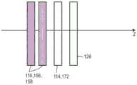
在WO 2012/110924 A1中(其内容通过引用包括在本文中)提出了一种用于光学检测至少一个对象的检测器。检测器包括至少一个光学传感器。光学传感器具有至少一个传感器区域。光学传感器被设计成以取决于传感器区域的照射的方式来生成至少一个传感器信号。给定照射的相同总功率,传感器信号取决于照射的几何形状,特别是取决于传感器区域上的照射的束横截面。此外,检测器具有至少一个评估装置。评估装置被设计成从传感器信号生成至少一项几何信息,特别是关于照射和/或对象的至少一项几何信息。In WO 2012/110924 A1, the content of which is incorporated herein by reference, a detector for optically detecting at least one object is proposed. The detector includes at least one optical sensor. The optical sensor has at least one sensor area. The optical sensor is designed to generate at least one sensor signal in a manner that depends on the illumination of the sensor area. Given the same total power of the illumination, the sensor signal depends on the geometry of the illumination and in particular on the beam cross-section of the illumination over the sensor area. Furthermore, the detector has at least one evaluation device. The evaluation device is designed to generate at least one piece of geometrical information from the sensor signal, in particular at least one piece of geometrical information about the illumination and/or the object.
2012年12月19日提交的美国临时申请61/739,173、2013年1月8日提交的61/749,964和2013年8月19日提交的61/867,169以及2013年12月18日提交的国际专利申请PCT/IB2013/061095(其公开为WO2014/097181A1)的全部内容全部内容通过引用并入本文,其公开了一种通过使用至少一个横向光学传感器和至少一个光学传感器来确定至少一个对象的位置的方法和检测器。具体地,公开了传感器堆叠的使用,以便以高精确度和无不确定性地确定对象的纵向位置。U.S. Provisional Application 61/739,173, filed December 19, 2012, 61/749,964, January 8, 2013, and 61/867,169, August 19, 2013, and International Patent Application, December 18, 2013 PCT/IB2013/061095 (published as WO2014/097181A1), which is incorporated herein by reference in its entirety, discloses a method of determining the position of at least one object by using at least one lateral optical sensor and at least one optical sensor and detector. Specifically, the use of a sensor stack is disclosed to determine the longitudinal position of an object with high accuracy and without uncertainty.
2013年6月13日提交的欧洲专利申请号为EP 13171898.3(其全部内容通过引用包含在本文中)公开了一种光学检测器,其包括具有基板和设置在其上的至少一个光敏层设置的光学传感器。光敏层设置具有至少一个第一电极、至少一个第二电极和夹在第一电极和第二电极之间的至少一种光伏材料。光伏材料包括至少一种有机材料。第一电极包括多个第一电极条,并且第二电极包括多个第二电极条,其中第一电极条和第二电极条以这种方式相交,即像素矩阵形成在第一电极条和第二电极条的交叉点处。光学检测器进一步包括至少一个读出装置,该读出装置包括连接到第二电极条的多个电测量装置和用于随后将第一电极条连接到电测量装置的开关装置。European Patent Application No. EP 13171898.3, filed on June 13, 2013, the entire content of which is incorporated herein by reference, discloses an optical detector comprising an arrangement having a substrate and at least one photosensitive layer disposed thereon. Optical sensor. The photoactive layer is provided with at least one first electrode, at least one second electrode, and at least one photovoltaic material sandwiched between the first electrode and the second electrode. The photovoltaic material includes at least one organic material. The first electrode includes a plurality of first electrode strips, and the second electrode includes a plurality of second electrode strips, wherein the first electrode strips and the second electrode strips intersect in such a way that a pixel matrix is formed between the first electrode strips and the second electrode strips. at the intersection of the two electrode strips. The optical detector further comprises at least one readout device comprising a plurality of electrical measurement devices connected to the second electrode strip and switching means for subsequently connecting the first electrode strip to the electrical measurement device.
同样于2013年6月13日提交的欧洲专利申请号EP 13171900.7(其全部内容通过引用包括在本文中)公开了一种用于确定至少一个对象的取向的检测器装置,包括至少两个信标装置,该至少两个信标装置适配于为附接到对象、由对象保持并且集成到对象中的至少一个,该信标装置每一个适配于将光束引向检测器,并且信标装置在对象的坐标系中具有预定的坐标。检测器装置进一步包括适配于检测从信标装置朝向检测器行进的光束的至少一个检测器以及至少一个评估装置,评估装置适配于确定在检测器的坐标系中的信标装置中的每一个信标装置的纵坐标。评估装置进一步适配于通过使用信标装置的纵坐标来确定检测器的坐标系中对象的取向。European Patent Application No. EP 13171900.7, also filed on June 13, 2013, the entire content of which is incorporated herein by reference, discloses a detector arrangement for determining the orientation of at least one object, comprising at least two beacons means, the at least two beacon means adapted to be attached to, held by, and integrated into at least one of the object, the beacon means each adapted to direct a light beam towards a detector, and the beacon means There are predetermined coordinates in the coordinate system of the object. The detector device further comprises at least one detector adapted to detect light beams travelling from the beacon device towards the detector and at least one evaluation device adapted to determine each of the beacon devices in the coordinate system of the detector. The ordinate of a beacon device. The evaluation device is further adapted to determine the orientation of the object in the coordinate system of the detector by using the ordinate of the beacon device.
于2013年6月13日提交的欧洲专利申请号EP 13171901.5(所有其全部内容通过引用包含在本文中)公开了一种用于确定至少一个对象的位置的检测器。检测器包括至少一个光学传感器,其适配于检测从对象朝向检测器行进的光束,光学传感器具有至少一个像素矩阵。检测器进一步包括至少一个评估装置,评估装置适配于确定由光束照射的光学传感器的像素的数量N。评估装置进一步适配于通过使用由光束照射的像素的数量N来确定对象的至少一个纵坐标。European Patent Application No. EP 13171901.5, filed June 13, 2013, the entire contents of which are incorporated herein by reference, discloses a detector for determining the position of at least one object. The detector comprises at least one optical sensor adapted to detect light beams travelling from the object towards the detector, the optical sensor having at least one matrix of pixels. The detector further comprises at least one evaluation device adapted to determine the number N of pixels of the optical sensor illuminated by the light beam. The evaluation device is further adapted to determine at least one ordinate of the object by using the number N of pixels illuminated by the light beam.
在本发明所引用的2014年8月15日提交的PCT/EP2014/067466中(其全部内容通过引用包含在本文中),提出了一种光学检测器。光学检测器包括至少一个空间光调制器,其适用于以空间分辨的方式修改光束的至少一个性质。空间光调制器具有像素矩阵,每个像素是可控制的以分别修改通过像素的光束的一部分的至少一个光学性质。光学检测器包括至少一个光学传感器,该光学传感器适用于在通过空间光调制器的像素矩阵之后检测光束并且产生至少一个传感器信号。光学检测器包括至少一个调制器装置,该调制器装置适用于周期性地控制具有不同调制频率的至少两个像素。光学检测器包括至少一个评估装置,适用于进行频率分析,以便确定用于调制频率的传感器信号的信号分量。In PCT/EP2014/067466, filed August 15, 2014, which is hereby incorporated by reference in its entirety, an optical detector is proposed. The optical detector includes at least one spatial light modulator adapted to modify at least one property of the light beam in a spatially resolved manner. The spatial light modulator has a matrix of pixels, each pixel controllable to individually modify at least one optical property of a portion of the light beam passing through the pixel. The optical detector includes at least one optical sensor adapted to detect the light beam after passing through the pixel matrix of the spatial light modulator and generate at least one sensor signal. The optical detector comprises at least one modulator device adapted to periodically control at least two pixels having different modulation frequencies. The optical detector comprises at least one evaluation device suitable for performing a frequency analysis in order to determine a signal component of the sensor signal for modulating the frequency.
尽管具有上述装置和检测器所暗指的优点,特别是由PCT/EP2014/067466、WO2012/110924 A1、US 61/739,173、US 61/749,964、EP 13171898.3、EP 13171900.7和EP13171901.5中公开的检测器具体表现出上述装置和检测器所暗示的优点,但是仍然存在若干技术挑战。因此,通常存在对于可靠的并且可以以低成本制造的用于检测对象在空间中的位置的检测器的需要。具体地,对于具有高分辨率的检测器存在强大的需求,以便生成关于对象的位置的图像和/或信息,其可以以高体积和低成本实现,并且仍提供高的分辨率和图像质量。Notwithstanding the advantages implied by the above devices and detectors, in particular the detections disclosed in PCT/EP2014/067466, WO2012/110924 A1, US 61/739,173, US 61/749,964, EP 13171898.3, EP 13171900.7 and EP13171901.5 Detectors specifically exhibit the advantages implied by the devices and detectors described above, but several technical challenges remain. Therefore, there is generally a need for a detector for detecting the position of an object in space that is reliable and can be manufactured at low cost. In particular, there is a strong need for detectors with high resolution in order to generate images and/or information about the position of objects, which can be implemented with high volume and low cost, and still provide high resolution and image quality.
发明内容SUMMARY OF THE INVENTION
因此,本发明的目的是提供面向已知装置和方法的上述技术挑战的装置和方法。具体地,本发明的目的是提供可靠地可确定空间中对象的位置的装置和方法,优选地以低技术努力和在技术资源和成本方面的低要求。Therefore, it is an object of the present invention to provide an apparatus and method that faces the above-mentioned technical challenges of known apparatus and methods. In particular, it is an object of the present invention to provide a device and a method that can reliably determine the position of an object in space, preferably with low technical effort and low requirements in terms of technical resources and costs.
该问题通过控制至少一个空间光调制器的像素的方法、光学检测的方法、用于控制至少一个空间光调制器的像素的调制器装置、用于空间光调制的调制器组件、光学检测器、检测器系统、光学检测方法、人机接口、娱乐装置、跟踪系统、检测系统、相机以及光学检测器的各种用途采用独立权利要求的特征来解决。在从属权利要求中列出了可能以孤立的方式或以任何任意组合实现的优选实施例。The problem is solved by a method of controlling a pixel of at least one spatial light modulator, a method of optical detection, a modulator device for controlling a pixel of at least one spatial light modulator, a modulator assembly for spatial light modulation, an optical detector, The various uses of detector systems, optical detection methods, human-machine interfaces, entertainment devices, tracking systems, detection systems, cameras and optical detectors are solved with the features of the independent claims. Preferred embodiments which may be realized in isolation or in any arbitrary combination are listed in the dependent claims.
如在下面使用的,术语“具有”、“包括”或“包含”或其任何的任意语法变体以非排它方式使用。因此,这些术语可指除了由这些术语引入的特征之外,没有其它特征存在在该上下文中描述的实体中的情况,以及是指存在一个或多个其它特征的情况。作为示例,表述“A具有B”、“A包括B”以及“A包含B”可以都指:即除了B之外,没有其它元件存在于A中的情况(即,A单独和排它地由B组成的情况);以及除了B之外,一个或多个其它元件,诸如元件C、元件C和D,或甚至其它元件,存在于实体A中的情况。As used below, the terms "having", "including" or "comprising" or any arbitrary grammatical variant thereof are used in a non-exclusive manner. Accordingly, these terms may refer to situations where no other feature is present in the entity described in this context, other than the feature introduced by these terms, and to a situation where one or more other features are present. As an example, the expressions "A has B," "A includes B," and "A includes B" may all refer to the fact that no elements other than B are present in A (ie, A alone and exclusively consists of the case where B consists of); and the case where, in addition to B, one or more other elements, such as element C, elements C and D, or even other elements, are present in entity A.
此外,如在下面使用的,术语“优选地”、“更优选地”、“特别地”、“更特别地”、“具体地”、“更具体地”或类似术语可结合可选特征使用,并不限制可替代的可能性。因此,由这些术语中引入的特征是可选的特征,并且不旨在以任何方式限制权利要求的范围。如本领域技术人员将认识的,本发明可以通过使用替代的特征来实施。同样地,由“在本发明的实施例中”或类似表述引入的特征旨在是可选特征,而没有关于本发明替代实施例的任何限制,没有关于本发明的范围的任何限制,并且没有关于将以这种方式引入的特征与本发明的其它可选或非可选特征组合的可能性的任何限制。Furthermore, as used below, the terms "preferably", "more preferably", "in particular", "more particularly", "specifically", "more specifically" or similar terms may be used in conjunction with optional features , without limiting the alternative possibilities. Accordingly, the features introduced by these terms are optional features and are not intended to limit the scope of the claims in any way. As those skilled in the art will recognize, the present invention may be practiced using alternative features. Likewise, features introduced by "in embodiments of the invention" or similar expressions are intended to be optional features without any limitation with respect to alternative embodiments of the invention, without any limitation with regard to the scope of the invention, and without Any limitation on the possibility of combining features introduced in this way with other optional or non-optional features of the invention.
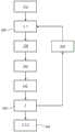
在本发明的第一方面,公开了一种控制至少一个空间光调制器的像素的方法。空间光调制器具有像素矩阵,每个像素可单独控制。该方法包括以下步骤,其可以按照给定的顺序或以不同的顺序进行。此外,两个或多个或甚至全部方法步骤可以同时进行和/或在时间上重叠而进行。此外,可以重复进行一个、两个或更多个或甚至所有的方法步骤。该方法还可以包括额外的方法步骤。该方法包括以下步骤:In a first aspect of the present invention, a method of controlling a pixel of at least one spatial light modulator is disclosed. Spatial light modulators have a matrix of pixels, each of which can be controlled individually. The method includes the following steps, which can be performed in a given order or in a different order. Furthermore, two or more or even all method steps may be performed simultaneously and/or overlapped in time. Furthermore, one, two or more or even all method steps may be repeated. The method may also include additional method steps. The method includes the following steps:
a)接收至少一个图像;a) receiving at least one image;
b)限定在图像内的至少一个图像段;b) at least one image segment defined within the image;
c)至少一个灰阶值分配给每个图像段;c) at least one grayscale value is assigned to each image segment;
d)将像素矩阵的至少一个像素分配给每个图像段;d) assigning at least one pixel of the pixel matrix to each image segment;
e)将独特调制频率分配给被分配给至少一个图像段的每个灰阶值;e) assigning a unique modulation frequency to each grayscale value assigned to at least one image segment;
f)以被分配给各自的图像段的独特调制频率来控制被分配给所述至少一个图像段的像素矩阵的所述至少一个像素。f) controlling the at least one pixel of the pixel matrix assigned to the at least one image segment with a unique modulation frequency assigned to the respective image segment.
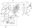
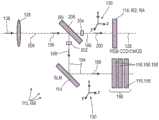
如本文进一步使用的,也称为SLM的“空间光调制器”通常是适用于以空间分辨的方式修改光束的至少一个性质(具体地至少一种光学性质)的装置,具体地,在与光束的传播方向成一角度的至少一个方向,其通常可以是由调制装置的类型确定的任意或合适的角度。该角度可以是90°或不同于90°,后者具体可能优选用于移动应用。例如,空间光调制器可以在垂直于光束的传播方向的至少一个方向上以空间分辨的方式修改光束的至少一个性质,具体地,至少一个光学性质。空间光调制器可以垂直于光束而安装。例如,空间光调制器可以由侧向的光束照射。因此,作为示例,空间光调制器可以适用于以受控的方式在垂直于光束的局部传播方向的平面中修改至少一个光学性质。因此,空间光调制器可以是能够对光束施加某种形式的空间变化调制的任意装置,优选地在垂直于光束的传播方向的至少一个方向上。可以以受控的方式修改至少一个性质的空间变化,使得在与传播方向垂直的平面中的每个可控位置处,空间光调制器可以采取至少两个状态,这些状态可以以不同的方式修改光束。As used further herein, a "spatial light modulator", also referred to as an SLM, is generally a device suitable for modifying in a spatially resolved manner at least one property, in particular at least one optical property, of a light beam, in particular in relation to a light beam The propagation direction of the at least one direction at an angle, which may generally be any or suitable angle determined by the type of modulation device. This angle may be 90° or different from 90°, the latter may in particular be preferred for mobile applications. For example, the spatial light modulator may modify at least one property of the light beam, in particular, at least one optical property, in a spatially resolved manner in at least one direction perpendicular to the direction of propagation of the light beam. The spatial light modulator can be mounted perpendicular to the beam. For example, the spatial light modulator may be illuminated by a sideways beam. Thus, as an example, a spatial light modulator may be adapted to modify at least one optical property in a controlled manner in a plane perpendicular to the local propagation direction of the light beam. Thus, a spatial light modulator may be any device capable of imparting some form of spatially varying modulation to a light beam, preferably in at least one direction perpendicular to the direction of propagation of the light beam. The spatial variation of at least one property can be modified in a controlled manner such that at each controllable location in a plane perpendicular to the direction of propagation, the spatial light modulator can assume at least two states, which can be modified in different ways beam.
空间光调制器在本领域中是众所周知的,例如在全息技术领域和/或投影仪装置领域。本领域通常已知的空间光调制器的简单实例是液晶空间调制器。透射和反射液晶空间光调制器都是已知的,并且可以在本发明中使用。此外,微机械空间光调制器基于可以单独控制的微镜的区域是已知的。因此,可以使用基于德州仪器公司提供的具有单色或多色甚至全色微镜的DLP技术的反射空间光调制器。此外,由V.Viereck等人(PhotonikInternational 2(2009),48-49)和/或US 7,677,742B2(Hillmer等人)公开的空间光调制器的微镜阵列可以用于本发明中。这里示出了能够在相对于光轴的平行和垂直位置之间切换微镜的微镜阵列。这些微镜阵列通常可以用作透明空间光调制器,类似于液晶技术上的透明空间光调制器空间。然而,这种类型的空间光调制器的透明度通常高于普通液晶空间光调制器的透明度。此外,空间光调制器可以基于诸如声光效应和/或诸如所谓的普克尔斯(Pockels)效应和/或所谓的克尔(Kerr)效应之类的电光效应的其它光学效应。此外,可以提供基于使用干涉式调制或IMOD技术的一个或多个空间光调制器。该技术基于每个像素内的可切换干扰效应。作为一个例子,后者由
此外,附加地或替代地,本文使用的至少一个空间光调制器可以是或可以包括可调谐光学元件的至少一个阵列,诸如下列的一个或多个:可调焦透镜阵列、自适应液体微透镜的区(area)、透明微棱镜阵列。可以使用可调谐光学元件的命名(named)阵列的任何组合。作为示例,阵列的光学元件的调谐可以电学地和/或光学地进行。作为示例,一个或多个可调谐光学元件阵列可以被放置在第一图像平面中,例如在诸如DLP、LCD、LCOS或其它SLM的其它空间光调制器中。可以调制诸如微透镜的光学元件的聚焦和/或诸如微棱镜的光学元件的折射。然后可以由至少一个光学传感器监视该调制并由至少一个评估装置进行评估(通过进行诸如解调的频率分析)。Additionally, or alternatively, at least one spatial light modulator as used herein may be or may include at least one array of tunable optical elements, such as one or more of the following: adjustable focus lens arrays, adaptive liquid microlenses area, transparent microprism array. Any combination of named arrays of tunable optical elements can be used. As an example, tuning of the optical elements of the array may be performed electrically and/or optically. As an example, one or more arrays of tunable optical elements may be placed in the first image plane, eg, in other spatial light modulators such as DLP, LCD, LCOS, or other SLMs. The focusing of optical elements such as microlenses and/or the refraction of optical elements such as microprisms can be modulated. The modulation can then be monitored by at least one optical sensor and evaluated by at least one evaluation device (by performing frequency analysis such as demodulation).
可调谐光学元件(例如聚焦可调透镜)提供了能够校正不同距离的对象具有不同焦点的事实的附加优点。作为示例的聚焦可调透镜阵列在US 2014/0132724A1中公开。其中公开的聚焦可调透镜阵列也可以用于根据本发明的光学检测器的SLM中。然而,其他实施例是可行的。此外,对于液体微透镜阵列的潜在示例,可以参考C.U.Murade等人的公开(Optics Express,Vol。20,No.16,18180-18187(2012))。再次,其他实施例是可行的。此外,对于诸如排列的电润湿微棱镜的微棱镜阵列的潜在示例,可以参考J.Heikenfeld等人的公开(Optics&Photonics News,2009年1月,20-26)。再次,可以使用微棱镜的其它实施例。Tunable optics, such as focus tunable lenses, offer the added advantage of being able to correct for the fact that objects at different distances have different focal points. An example focus tunable lens array is disclosed in US 2014/0132724 A1. The focus tunable lens array disclosed therein can also be used in the SLM of the optical detector according to the present invention. However, other embodiments are possible. Furthermore, for potential examples of liquid microlens arrays, reference may be made to the publication of C.U. Murad et al. (Optics Express, Vol. 20, No. 16, 18180-18187 (2012)). Again, other embodiments are possible. Furthermore, for potential examples of microprism arrays such as aligned electrowetting microprisms, reference may be made to the publication of J. Heikenfeld et al. (Optics & Photonics News, Jan 2009, 20-26). Again, other embodiments of microprisms can be used.
因此,作为示例,可以使用从由空间光调制器或反射空间光调制器组成的组中选择的一个或多个空间光调制器。此外,作为示例,可以使用从由以下各项组成的组中选择的一个或多个空间光调制器:基于液晶技术的空间光调制器,诸如一个或多个液晶空间光调制器;基于微机械系统的空间光调制器,例如基于微镜系统的空间光调制器,特别是微镜阵列;基于干涉调制的空间光调制器;基于声光效应的空间光调制器;基于电光效应的空间光调制器,具体地基于普克尔斯(Pockels)效应和/或克尔(Kerr)效应;包括可调谐光学元件的至少一个阵列的空间光调制器,诸如下列的一个或多个:可调焦透镜阵列、自适应液体微透镜的区、透明微棱镜阵列。本领域已知的典型的空间光调制器适用于调制光束强度的空间分布,例如在垂直于光束传播方向的平面中。然而,如下面将进一步详细描述的,另外或替代地,光束的其它光学性质可以是变化的,例如光束的相位和/或光束的颜色。下面将更详细地解释其他潜在的空间光调制器。Thus, as an example, one or more spatial light modulators selected from the group consisting of spatial light modulators or reflective spatial light modulators may be used. Furthermore, as an example, one or more spatial light modulators selected from the group consisting of: liquid crystal technology based spatial light modulators, such as one or more liquid crystal spatial light modulators; micromechanical based spatial light modulators, may be used System spatial light modulators, such as spatial light modulators based on micromirror systems, especially micromirror arrays; spatial light modulators based on interferometric modulation; spatial light modulators based on acousto-optic effects; spatial light modulation based on electro-optic effects a spatial light modulator, in particular based on the Pockels effect and/or the Kerr effect; a spatial light modulator comprising at least one array of tunable optical elements, such as one or more of the following: tunable focus lenses Arrays, zones of adaptive liquid microlenses, transparent microprism arrays. Typical spatial light modulators known in the art are suitable for modulating the spatial distribution of beam intensity, eg in a plane perpendicular to the beam propagation direction. However, as will be described in further detail below, additionally or alternatively, other optical properties of the light beam may be varied, such as the phase of the light beam and/or the color of the light beam. Other potential spatial light modulators will be explained in more detail below.
通常,空间光调制器可以是计算机可控的,使得光束的至少一个性质的变化状态可以由计算机调节。空间光调制器可以是电寻址空间光调制器、光寻址空间光调制器或任何其他类型的空间光调制器。Typically, the spatial light modulator can be computer controllable such that the changing state of at least one property of the light beam can be adjusted by the computer. The spatial light modulator may be an electrically addressed spatial light modulator, an optically addressed spatial light modulator, or any other type of spatial light modulator.
如上所述,空间光调制器包括像素矩阵,每个像素可被控制以单独修改通过像素的光束的一部分的至少一个光学性质,即通过穿过像素与像素相互作用,由像素反映或其他交互方式。如本文所使用的,“像素”因此通常是指适用于修改通过像素的光束的部分的至少一个光学性质的空间光调制器的整体元件。因此,像素可以是空间光调制器的最小单位,其适用于修改通过像素的光束的该部分的至少一个光学性质。作为示例,每个像素可以是液晶单元和/或微镜。每个像素可以单独控制。例如,每个像素可以包括至少一个微镜。As mentioned above, the spatial light modulator comprises a matrix of pixels, each pixel can be controlled to individually modify at least one optical property of a portion of the light beam passing through the pixel, ie by interacting with the pixel through the pixel, reflected by the pixel or otherwise interacting . As used herein, "pixel" thus generally refers to an integral element of a spatial light modulator suitable for modifying at least one optical property of a portion of a light beam passing through the pixel. Thus, a pixel may be the smallest unit of a spatial light modulator suitable for modifying at least one optical property of the portion of the light beam passing through the pixel. As an example, each pixel may be a liquid crystal cell and/or a micromirror. Each pixel can be controlled individually. For example, each pixel may include at least one micromirror.
如本文所使用的,术语“控制”通常是指像素修改至少一个光学性质的方式可被调整为呈现至少两个不同的状态。调整可以通过任何类型的控制进行,优选通过电调节。因此,优选地,每个像素可以单独地电寻址,以便例如通过向像素施加特定电压和/或特定电流来调整各个像素的状态。As used herein, the term "controlling" generally refers to the manner in which a pixel modifies at least one optical property can be adjusted to assume at least two different states. Adjustment can be done by any type of control, preferably by electrical regulation. Thus, each pixel is preferably individually electrically addressable in order to adjust the state of each pixel, eg by applying a specific voltage and/or a specific current to the pixel.
如本文进一步使用的,术语“单独”通常是指矩阵的一个像素可以至少基本上独立于寻址其他像素来寻址,使得像素的状态以及从而各自的像素影响光束的各自部分的方式,可以独立于一个或多个或甚至所有其他像素的实际状态来调整。As further used herein, the term "individually" generally means that one pixel of the matrix can be addressed at least substantially independently of addressing other pixels, such that the state of the pixel, and thus the manner in which the respective pixel affects the respective portion of the light beam, can be independently adjusted to the actual state of one or more or even all other pixels.
如本文所使用的,“接收至少一个图像”通常是指至少一个图像是下列的至少一个的事实:被提供、被记录、被接受、被读入和被获得。因此,例如,可以从数据存储器和/或成像装置等提供至少一个图像,例如,可以由CMOS和/或CCD和/或其他像素化图像传感器提供至少一个图像。至少一个图像可以是场景和/或至少一个对象的至少一个规则的二维图像。至少一个图像可以是或可以包括至少一个单色图像和/或至少一个多色图像和/或至少一个全色图像。此外,至少一个图像可以是或可以包括单个图像,或者可以包括图像的序列(sequence)。As used herein, "receiving at least one image" generally refers to the fact that at least one image is at least one of: provided, recorded, received, read in, and obtained. Thus, for example, the at least one image may be provided from a data store and/or an imaging device or the like, eg, the at least one image may be provided by a CMOS and/or CCD and/or other pixelated image sensor. The at least one image may be at least one regular two-dimensional image of the scene and/or at least one object. The at least one image may be or may include at least one monochrome image and/or at least one polychromatic image and/or at least one panchromatic image. Furthermore, at least one image may be or include a single image, or may include a sequence of images.
如本文所使用的,“至少一个图像段”是指图像的至少一部分和/或至少一个区和/或至少一个部。具体地,至少一个图像段可以对应于场景和/或至少一个对象或其部分。例如,至少一个图像可以包括对应于至少一个场景和/或至少一个对象或其部分的的至少一个区。至少一个图像可以包括两个或更多个图像段。如本文所使用的,“限定至少一个图像段”是指挑选和/或选择和/或识别图像内的至少一部分和/或至少一个区和/或至少一个部。As used herein, "at least one image segment" refers to at least a portion and/or at least one region and/or at least one portion of an image. In particular, at least one image segment may correspond to a scene and/or at least one object or part thereof. For example, at least one image may comprise at least one region corresponding to at least one scene and/or at least one object or part thereof. At least one image may include two or more image segments. As used herein, "defining at least one image segment" refers to picking and/or selecting and/or identifying at least a portion and/or at least one region and/or at least one portion within an image.
如本文所使用的,术语“至少一个灰阶值”是指灰阶值或灰度级(这些术语通常和以下同义地使用),即一种或多种颜色的不同亮度级别。然而,原则上,在这种情况下,术语灰度级或灰阶值应被广泛地解释,,例如,还包括不同的亮度级别。灰阶值可以在黑色(在色彩颜色“黑色”的情况下应相应地被理解为意味着最黑暗的水平)和白色(在色彩颜色“白色”的情况下应相应地被理解为是最轻的水平)之间。灰阶值可以是颜色值和/或灰阶值。As used herein, the term "at least one grayscale value" refers to a grayscale value or grayscale (these terms are often used synonymously below), ie, different brightness levels of one or more colors. In principle, however, in this case the term greyscale or greyscale value should be interpreted broadly, eg also including different brightness levels. The grayscale value can be understood in the case of black (in the case of the chromatic color "black" should correspondingly be understood to mean the darkest level) and white (in the case of the chromatic color "white" should correspondingly be understood as the lightest level) level). Grayscale values may be color values and/or grayscale values.
如本文所使用的,“分配至少一个灰度值”是指对于每个图像段选择和/或确定灰阶值。特别地,至少一个图像可以被编码为灰阶图像。灰度值可以在这些黑色和白色限制值之间的以离散阶梯分配。例如,灰度值可以以灰度级别阶梯分配,其具有从黑色到白色的恒定的预限定的间隔。可预先限定可能的灰阶值的离散数量。因此,例如,在图像包括两个图像段的情况下,对于两个图像段中的每一个,可以分配与另一图像段的灰度值不同的至少一个灰度值。As used herein, "assigning at least one grayscale value" refers to selecting and/or determining a grayscale value for each image segment. In particular, at least one image may be encoded as a grayscale image. Grayscale values can be distributed in discrete steps between these black and white limit values. For example, grayscale values may be assigned in grayscale steps with constant predefined intervals from black to white. The discrete number of possible grayscale values can be predefined. Thus, for example, in the case of an image comprising two image segments, for each of the two image segments, at least one grayscale value may be assigned that differs from the grayscale value of the other image segment.
如本文所使用的,“将至少一个像素分配给每个图像段”是指将空间光调制器的至少一个像素与至少一个图像段进行匹配。每个像素可以单独地匹配于图像段和/或一组像素,例如,至少两个像素可以一起匹配到图像段。因此,可选地,图像和/或图像段被映射到像素矩阵上。优选地,至少一个图像被像素化,使得图像与像素矩阵完全匹配,从而产生像素化图像。As used herein, "assigning at least one pixel to each image segment" refers to matching at least one pixel of the spatial light modulator with at least one image segment. Each pixel may be individually matched to an image segment and/or a group of pixels, eg, at least two pixels may be matched to an image segment together. Thus, optionally, images and/or image segments are mapped onto pixel matrices. Preferably, at least one image is pixelated such that the image exactly matches the pixel matrix, resulting in a pixelated image.
如本文所使用的,“分配独特调制频率”是指将至少一个频率与至少一个灰阶值进行匹配。如本文所使用的,术语“独特调制频率”通常是指调制的频率f和像素的控制的调制的相位
术语“控制”包括选择每个单独的像素和/或一组像素并改变所选择的像素和/或一组像素的状态。控制可以是周期性的,特别是单独的。可以周期性地进行各个像素的至少两个不同状态之间的切换,其中就其与通过像素的光束的部分相互作用的方式而言,各自的像素的至少两个不同状态不相同,从而,就其改变通过像素的光束的部分的程度或方式而言,不相同。独特调制频率通常从由各自的像素的至少两个状态之间的周期性切换的相位和/或频率组成的组中选择。切换通常可以是逐步切换或数字切换,或者可以是其中各个像素的状态在第一状态和第二状态之间连续地改变的连续切换。作为最常见的示例,像素可以在各个调制频率,即在特定频率f和/或特定相位
步骤f)可以包括以下子步骤:Step f) may comprise the following sub-steps:
f1.向独特调制频率分配计数器阈值;f1. Assign counter thresholds to unique modulation frequencies;
f2.以预定的最大频率逐步增加计数器变量,直到达到或超过阈值为止;f2. Increment the counter variable incrementally at a predetermined maximum frequency until the threshold is reached or exceeded;
f3.改变像素的状态。f3. Change the state of the pixel.
子步骤可以以给定的顺序或以不同的顺序进行。此外,两个或更多个或甚至全部子步骤可以同时进行和/或在时间上重叠。此外,可以重复进行一个、两个或更多个或甚至全部子步骤。步骤f)还可以包括额外的方法步骤。The sub-steps can be performed in a given order or in a different order. Furthermore, two or more or even all of the sub-steps may be performed simultaneously and/or overlap in time. Furthermore, one, two or more or even all of the sub-steps may be repeated. Step f) may also comprise additional method steps.
如本文所使用的,术语“计数器变量”是指可以逐步增加的整数。如本文所使用的,术语“计数器阈值”是指计数器变量的指定和/或预定阈值。在计数器变量超过计数器阈值的情况下,可以改变像素的状态。预定的最大频率可以是用于改变像素的状态的最大频率f0,其导致由像素调制的光束的区的最大光频率f0/2。例如,对于像素的亮暗变化,可能需要像素的两个变化,首先是亮的,其次是暗的。可以相对于扫描时间TA=1/f0增加计数器。扫描时间可以是在一个图像缓冲内处理一个图像所需的时间,特别是用于进行方法步骤a)至f)以及可调延迟时间,例如,调整所需的时间。例如,可以以扫描时间的间隔和/或以多个扫描时间的间隔来增加计数器变量。低阈值可能导致改变像素的状态的高频率,并且因此导致短的时间间隔。高阈值可能导致改变像素状态的低频率,并因此导致长时间间隔,而可以通过选择f0来设置实际持续时间。最低阈值可以指扫描时间的单个间隔。As used herein, the term "counter variable" refers to an integer that can be incremented in steps. As used herein, the term "counter threshold" refers to a specified and/or predetermined threshold for a counter variable. In the event that the counter variable exceeds the counter threshold, the state of the pixel can be changed. The predetermined maximum frequency may be the maximum frequency f0 for changing the state of the pixel, which results in the maximum optical frequency f0/2 of the region of the light beam modulated by the pixel. For example, for a light-dark change of a pixel, two changes of the pixel may be required, first light and second dark. The counter can be incremented relative to the scan time TA =1/f0 . The scan time can be the time required to process an image in an image buffer, in particular for carrying out method steps a) to f) and the adjustable delay time, eg the time required for adjustment. For example, the counter variable may be incremented at scan time intervals and/or at multiple scan time intervals. A low threshold may result in a high frequency of changing the state of a pixel, and thus a short time interval. A high threshold can result in a low frequency of changing pixel states and thus long intervals, whereas the actual duration can be set by choosingf0 . The lowest threshold can refer to a single interval of scan time.
用于改变像素状态的可行独特调制频率fn可以由fn=f0/2n确定,其中n是非零整数。例如,f0可以是24kHz。因此,可以以12kHz的最大频率改变像素状态。灰阶值的总数可以取决于可行独特频率的总数。可行频率可能高于最低频率。最小频率可以是高于该频率的两个相邻可行频率是可区分和/或可分辨的频率。可能的频率可能必须具有等于最小距离或超过最小距离的相邻可行频率。Possible unique modulation frequencies fn for changing pixel states can be determined by fn =f0 /2n, where n is a non-zero integer. For example, f0 may be 24kHz. Therefore, the pixel state can be changed with a maximum frequency of 12kHz. The total number of grayscale values may depend on the total number of feasible unique frequencies. The feasible frequency may be higher than the minimum frequency. The minimum frequency may be the frequency above which two adjacent feasible frequencies are distinguishable and/or distinguishable. Possible frequencies may have to have adjacent feasible frequencies equal to or exceeding the minimum distance.
空间光调制器的每个像素可以具有至少两个状态。在步骤f)中,像素可以从第一状态切换到第二状态,反之亦然。像素的实际状态可以以受控的方式可调节,其中对于每个像素,该至少两个状态就其相对于通过各自的像素的光束的部分与各自像素的的相互作用而言是不同的,例如就下面的一者或多者而言是不同的:光束的该部分与像素的吸收、透射、反射、相变或任何其它类型的相互作用而言是不同的。例如,像素的第一状态可以是关闭状态,并且像素的第二状态可以是开启状态。在像素处于关闭状态的情况下,防止光的部分向着例如将在下面详细描述的光学传感器的方向移动。在开启状态下,由像素反射的光可以朝着光学检测器进行。Each pixel of the spatial light modulator can have at least two states. In step f), the pixel can be switched from the first state to the second state and vice versa. The actual state of a pixel can be adjusted in a controlled manner, wherein for each pixel the at least two states are different with respect to its interaction with the respective pixel relative to the portion of the light beam passing through the respective pixel, e.g. Different in terms of one or more of the following: the portion of the light beam is different in terms of absorption, transmission, reflection, phase change, or any other type of interaction with the pixel. For example, the first state of the pixel may be the off state and the second state of the pixel may be the on state. With the pixel in the off state, the portion of the light is prevented from moving in the direction of, for example, the optical sensor, which will be described in detail below. In the on state, the light reflected by the pixel can proceed towards the optical detector.
如上所述,由空间光调制器给出的最大频率可以限制可行独特频率的数量。作为示例,可以通过使用一个、两个、三个或更多个沃尔什函数,特别是沃尔什系统,来确定用于改变像素的状态的可行的独特调制频率。如本文所使用的,并且在https://en.wikipedia.org/wiki/Walsh_function下更详细地描述,术语“沃尔什函数”通常是指单位区间的三角函数的连续模拟系统的离散数字对应物间隔。与三角函数不同,沃尔什函数通常只是分段连续的,实际上是分段常数。函数通常在二进制分数限定的子时间间隔内取值-1和+1。沃尔什函数通常形成一个完整的正交函数集合,在单位区间单位区间上的平方积分函数的希尔伯特空间L2[0,1]中的正交基。两者通常都是有界函数的系统。这三角系统(system)和沃尔什系统二者周期性地承认从单位区间的到实线(real line)的自然延伸(natural extension)。此外,对于单位区间(傅里叶级数)和实线(傅里叶变换)的傅里叶分析通常都通过沃尔什系统限定的数字对应物、类似于傅里叶级数的沃尔什级数和类似于傅立叶变换的哈达玛变换。沃尔什函数、级数和变换在物理和工程领域(特别是数字信号处理)可以寻找到各种应用。As mentioned above, the maximum frequency given by the spatial light modulator can limit the number of feasible unique frequencies. As an example, feasible unique modulation frequencies for changing the state of a pixel can be determined by using one, two, three or more Walsh functions, particularly Walsh systems. As used herein, and described in more detail under https://en.wikipedia.org/wiki/Walsh_function, the term "Walsh function" generally refers to the discrete numerical counterpart of a continuous analog system of trigonometric functions of the unit interval object interval. Unlike trigonometric functions, Walsh functions are usually only piecewise continuous and are actually piecewise constant. The function typically takes values -1 and +1 in subintervals defined by binary fractions. Walsh functions generally form a complete set of orthogonal functions, orthonormal bases in the Hilbert space L2 [0,1] of square integral functions over unit intervals. Both are generally systems of bounded functions. Both the triangular system and the Walsh system periodically admit a natural extension from the unit interval to the real line. In addition, Fourier analysis for both unit interval (Fourier series) and solid line (Fourier transform) is usually done through the numerical counterparts defined by the Walsh system, Walsh analogous to the Fourier series Series and Hadamard Transform similar to Fourier Transform. Walsh functions, series and transformations find various applications in the fields of physics and engineering (especially digital signal processing).
与如上所述的使用整数除法相比,使用沃尔什函数可以获得更多数量的用于改变像素的状态的可行独特调制频率,其具有由空间光调制器给出的相同最大频率。因此,可能使用具有较低的最大频率的空间光调制器,例如,最大频率为2kHz的空间光调制器。Using the Walsh function can obtain a greater number of feasible unique modulation frequencies for changing the state of a pixel, with the same maximum frequency given by the spatial light modulator, than using integer division as described above. Therefore, it is possible to use a spatial light modulator with a lower maximum frequency, eg a spatial light modulator with a maximum frequency of 2 kHz.
在步骤e)中,对于每个灰阶值,一个沃尔什函数可被分配给至少一个图像段。在步骤b)中限定多个段的情况下,可以选择适当的沃尔什函数集合。可以考虑所使用的函数的总数量和使用的沃尔什函数之间的噪声来选择沃尔什函数,其中所需的函数的总数可以对应于所限定的段的数量。优选地,相邻沃尔什函数可以具有尽可能少的噪声。此外,沃尔什变换可以使用整个谱范围,使得与傅里叶变换相比,可以在频率之间发生较少的噪声。为了对抗扰动是可靠的,沃尔什函数可以被选择为具有长的平台(plateau),因此几乎不过零。In step e), for each grayscale value, a Walsh function can be assigned to at least one image segment. Where multiple segments are defined in step b), an appropriate set of Walsh functions can be selected. The Walsh functions may be chosen taking into account the total number of functions used and the noise between the Walsh functions used, wherein the total number of functions required may correspond to the number of defined segments. Preferably, adjacent Walsh functions can have as little noise as possible. Furthermore, the Walsh transform can use the entire spectral range so that less noise can occur between frequencies compared to the Fourier transform. In order to be robust against perturbations, the Walsh function can be chosen to have a long plateau and thus be nearly zero.
在步骤f)中,可以使用沃尔什函数作为独特的调制频率来控制至少一个像素。如上所述,像素可以具有两个状态。在如上所述使用整数除法的情况下,可以将像素的状态从第一状态切换到第二状态,反之亦然,例如从开启状态切换到关闭状态,或从关闭状态切换到开启状态。在使用沃尔什函数的情况下,像素的状态不仅可以在开启或关闭状态之间变化,而且可以根据由某个沃尔什函数给出的模式(pattern)来切换像素的状态。例如,在一段时间内,例如,允许像素状态的五个改变的一定时间间隔,像素的状态可以根据off、off、on、on、on而变化。其他模式当然可行。In step f), at least one pixel can be controlled using the Walsh function as the unique modulation frequency. As mentioned above, a pixel can have two states. Where integer division is used as described above, the state of a pixel can be switched from a first state to a second state and vice versa, eg from an on state to an off state, or from an off state to an on state. In the case of using a Walsh function, the state of a pixel can not only change between on or off states, but also switch the state of the pixel according to a pattern given by some Walsh function. For example, over a period of time, eg, a certain time interval allowing five changes of the pixel state, the state of the pixel may change according to off, off, on, on, on. Other modes are certainly possible.
如上所述,灰阶值可以是颜色值和/或灰度值。As mentioned above, the grayscale values may be color values and/or grayscale values.
步骤a)可以包括提供图像的序列。如本文所使用的,“图像的序列”是指在步骤a)中接收至少两个图像的事实。可以对图像序列的每个图像重复步骤b)-f)。图像序列可以包括视频。Step a) may comprise providing a sequence of images. As used herein, "sequence of images" refers to the fact that at least two images are received in step a). Steps b)-f) can be repeated for each image of the sequence of images. The sequence of images may include video.
步骤a)可以包括将至少一个图像提供给调制器装置,其中步骤b)-f)可以由调制器装置进行。关于调制器装置,可以参考以下给出的调制器装置的描述。Step a) may comprise providing at least one image to the modulator device, wherein steps b)-f) may be performed by the modulator device. Regarding the modulator device, reference can be made to the description of the modulator device given below.
步骤a)可以包括在调制器装置的至少一个图像缓冲器中缓冲至少一个图像。如本文所使用的,术语“图像缓冲器”是指适用于接收至少一个图像的数据存储装置。图像缓冲器可以适用于在一定时间内存储至少一个图像。图像缓冲器可以适用于将至少一个图像提供给调制器装置的其他装置,特别是用于进行方法步骤b)至f)。在步骤a)中,可以使用至少两个图像缓冲器。图像缓冲器可以包括第一图像缓冲器和第二图像缓冲器,其中第一图像缓冲器和第二图像缓冲器可以从由有源(active)图像缓冲器和非有源图像缓冲器组成的组中选择。至少一个图像可以被缓存在非有源图像缓冲器和有源图像缓冲器中的一个或两个中。可以选择非有源图像缓冲器以进一步评估在有源图像缓冲器内缓冲的至少一个图像,其中至少第二图像可以被接收并且可以被缓冲在有源图像缓冲器中,同时评估在有源图像缓冲区内的至少一个图像。因此,通过使用至少两个图像缓冲器,可以在同一时间或短时间内接收多个图像。因此,可以高速地读取多个图像。在多个图像中读取的帧速率可以在20和250Hz之间,优选在50和200Hz之间,更优选在80和120Hz之间,例如100Hz。通常,帧速率可能受到图像缓冲器的存储带宽和/或其他技术因素的限制和/或依赖于图像缓冲器的存储带宽和/或其他技术因素,其他技术因素例如为FPGA的门运行时间等。然而,通过使用具有较高复杂度的硬件,例如专用集成电路(ASIC)和/或VLSI-IC。例如,帧速率可以对应于和/或可以是成像装置(例如摄像机)的图像输出的倍数,从成像装置接收图像。Step a) may comprise buffering the at least one image in at least one image buffer of the modulator device. As used herein, the term "image buffer" refers to a data storage device suitable for receiving at least one image. The image buffer may be adapted to store at least one image within a certain period of time. The image buffer may be adapted to provide at least one image to other devices of the modulator device, in particular for carrying out method steps b) to f). In step a), at least two image buffers can be used. The image buffer may include a first image buffer and a second image buffer, wherein the first image buffer and the second image buffer may be selected from the group consisting of active image buffers and non-active image buffers in the selection. At least one image may be buffered in one or both of the non-active image buffer and the active image buffer. The non-active image buffer may be selected for further evaluation of the at least one image buffered within the active image buffer, wherein at least a second image may be received and may be buffered in the active image buffer while evaluating the active image buffer. At least one image in the buffer. Therefore, by using at least two image buffers, multiple images can be received at the same time or within a short period of time. Therefore, a plurality of images can be read at high speed. The frame rate at which the multiple images are read may be between 20 and 250 Hz, preferably between 50 and 200 Hz, more preferably between 80 and 120 Hz, eg 100 Hz. In general, the frame rate may be limited by and/or depend on the memory bandwidth of the image buffer and/or other technical factors, such as the gate runtime of the FPGA, etc. However, by using hardware with higher complexity, such as application specific integrated circuits (ASICs) and/or VLSI-ICs. For example, the frame rate may correspond to and/or may be a multiple of the image output of the imaging device (eg, camera) from which the image is received.
如上所述,每个像素可以包括至少一个微镜。As described above, each pixel may include at least one micromirror.
在本发明的另一方面,公开了一种光学检测方法,特别是一种用于确定至少一个对象的位置的方法。该方法包括以下步骤,其可以按照给定的顺序或以不同的顺序进行。此外,两个或多个或甚至全部方法步骤可以同时进行和/或在时间上重叠。此外,可以重复进行一个、两个或更多个或甚至所有的方法步骤。该方法还可以包括额外的方法步骤。该方法包括以下方法步骤:In another aspect of the present invention, an optical detection method is disclosed, in particular a method for determining the position of at least one object. The method includes the following steps, which can be performed in a given order or in a different order. Furthermore, two or more or even all method steps may be performed simultaneously and/or overlap in time. Furthermore, one, two or more or even all method steps may be repeated. The method may also include additional method steps. The method includes the following method steps:
-通过使用至少一个空间光调制器以空间分辨的方式修改光束的至少一个性质,所述空间光调制器具有像素矩阵,每个像素可控制以单独地修改通过像素的光束的部分的至少一个光学性质,其中,使用了如上所述的控制像素的方法;- modifying at least one property of the light beam in a spatially resolved manner by using at least one spatial light modulator having a matrix of pixels, each pixel controllable to individually modify at least one optical property of the portion of the light beam passing through the pixel properties, wherein a method of controlling pixels as described above is used;
-通过使用至少一个光学传感器检测通过空间光调制器的像素矩阵的光束并且用于生成至少一个传感器信号;- detection of the light beam passing through the pixel matrix of the spatial light modulator by using at least one optical sensor and for generating at least one sensor signal;
-通过使用至少一个调制器装置以不同频率周期性地控制至少两个像素;和- periodically controlling at least two pixels at different frequencies by using at least one modulator device; and
-通过使用至少一个评估装置进行频率分析和确定控制频率的传感器信号的信号分量。- by using at least one evaluation device to perform a frequency analysis and to determine the signal component of the sensor signal of the control frequency.
该方法优选地可以通过使用根据本发明的光学检测器来进行,例如在以下给出的一个或多个实施例中所公开的。因此,关于该方法的限定和潜在实施例,可以参考光学检测器。仍然,其他实施例是可行的。此外,使用了根据本发明的控制像素的方法。因此,关于光学检测方法的限定和潜在实施例,可以参考下面给出的方法。仍然,其他实施例是可行的。The method can preferably be carried out by using an optical detector according to the present invention, such as disclosed in one or more of the examples given below. Accordingly, reference may be made to optical detectors for definitions and potential embodiments of the method. Still, other embodiments are possible. Furthermore, the method of controlling pixels according to the present invention is used. Therefore, with regard to definitions and potential embodiments of optical detection methods, reference may be made to the methods given below. Still, other embodiments are possible.
在本发明的另一方面,公开了一种用于控制至少一个空间光调制器的像素的调制器装置。空间光调制器具有像素矩阵,每个像素可单独控制。调制器装置包括:In another aspect of the invention, a modulator device for controlling a pixel of at least one spatial light modulator is disclosed. Spatial light modulators have a matrix of pixels, each of which can be controlled individually. The modulator device includes:
a)适用于接收至少一个图像的至少一个接收装置;a) at least one receiving device adapted to receive at least one image;
b)至少一个图像段限定装置,其适用于限定在所述图像内的至少一个图像段;b) at least one image segment defining means adapted to define at least one image segment within said image;
c)至少一个灰阶值分配装置,其适用于将至少一个灰阶值分配给每个图像段(灰阶值;c) at least one grayscale value assigning means adapted to assign at least one grayscale value to each image segment (grayscale value;
d)至少一个像素分配装置,其适用于将所述像素矩阵的至少一个像素分配给每个图像段;d) at least one pixel assignment means adapted to assign at least one pixel of said pixel matrix to each image segment;
e)至少一个频率分配装置,其适用于将独特调制频率分配给被分配给所述至少一个图像段的每个灰阶值;e) at least one frequency assigning means adapted to assign a unique modulation frequency to each grayscale value assigned to said at least one image segment;
f)至少一个控制装置,其适用于以被分配给各自的图像段的所述独特调制频率来控制被分配给所述至少一个图像段的像素矩阵的所述至少一个像素段。f) at least one control device adapted to control said at least one pixel segment of the pixel matrix assigned to said at least one image segment with said unique modulation frequency assigned to said at least one image segment.
调制器装置可以适用于进行根据本发明的控制像素的方法。此外,调制器装置可以用于根据本发明的光学检测方法中。关于定义和实施例,可以参考上面给出的用于控制像素和光学检测方法的方法的定义和实施例,以及下面给出的装置的定义和实施例。The modulator device may be adapted to carry out the method of controlling a pixel according to the invention. Furthermore, the modulator device can be used in the optical detection method according to the invention. With regard to definitions and embodiments, reference may be made to the definitions and embodiments of the method for controlling pixels and optical detection methods given above, and the definitions and embodiments of the apparatus given below.
如在本发明中所使用的,“调制器装置”通常是指适用于控制矩阵的两个或更多个或甚至全部像素的装置,以便调整相应的像素以将对于每个像素的不同状态的至少两个状态中的一个呈现,每个状态具有与通过各自的像素的光束的部分与像素相互作用的特定类型。因此,作为示例,调制器装置可以适用于选择性地将两种不同类型的电压和/或至少两种不同类型的电流施加到由调制器装置控制的每个像素。As used in the present invention, "modulator device" generally refers to a device suitable for controlling two or more, or even all pixels of a matrix, in order to adjust the corresponding pixels to adjust the corresponding pixels to the different states of each pixel. One of at least two states is present, each state having a particular type of interaction with the pixel with the portion of the light beam passing through the respective pixel. Thus, as an example, the modulator device may be adapted to selectively apply two different types of voltages and/or at least two different types of current to each pixel controlled by the modulator device.
至少一个调制器装置适用于周期性地控制至少两个像素,优选具有不同调制频率的矩阵中的更多像素或甚至所有像素。The at least one modulator device is adapted to periodically control at least two pixels, preferably more pixels or even all pixels in the matrix with different modulation frequencies.
如本文所使用的,“至少一个接收装置”通常是适用于接收至少一个图像的装置。特别地,至少一个接收装置适用于进行如上所述的方法步骤a)。如上面关于控制像素的方法所概述的,术语“接收至少一个图像”通常是指至少一个图像是被提供的、记录的、接受的和获得的至少一个图像的事实。用于接收至少一个图像的频率可以在60和120Hz之间。接收装置可以包括用于接收或传送图像的端口,例如,LCD端口。As used herein, "at least one receiving device" is generally a device adapted to receive at least one image. In particular, at least one receiving device is suitable for carrying out method step a) as described above. As outlined above with respect to the method of controlling pixels, the term "receiving at least one image" generally refers to the fact that at least one image is provided, recorded, received and obtained. The frequency for receiving the at least one image may be between 60 and 120 Hz. The receiving device may include a port for receiving or transmitting images, eg, an LCD port.
至少一个接收装置可以被连接或并入至少一个包括至少一个图像的数据存储装置。附加地或替代地,调制器装置可以连接或并入成像装置等,例如,CMOS,其适用于提供至少一个图像。At least one receiving device may be connected or incorporated into at least one data storage device comprising at least one image. Additionally or alternatively, the modulator device may be connected to or incorporated into an imaging device or the like, eg, a CMOS, suitable for providing at least one image.
接收装置可以包括至少一个图像缓冲器。优选地,接收装置可以包括至少两个图像缓冲器。图像缓冲器可以包括第一图像缓冲器和第二图像缓冲器,其中第一图像缓冲器和第二图像缓冲器可以从由有源图像缓冲器和非有源图像缓冲器组成的组中选择。接收装置可以适用于缓冲非有源图像缓冲器和有源图像缓冲器中的一个或两个中的至少一个图像。接收装置可以适用于选择非有源图像缓冲器以进一步评估在有源图像缓冲器内缓冲的至少一个图像,其中接收装置可以适用于接收和缓冲有源图像缓冲器中的至少第二图像,同时评估在有源图像缓冲器内缓冲的至少一个图像。The receiving means may comprise at least one image buffer. Preferably, the receiving means may comprise at least two image buffers. The image buffers may include a first image buffer and a second image buffer, wherein the first image buffer and the second image buffer may be selected from the group consisting of active image buffers and non-active image buffers. The receiving means may be adapted to buffer at least one image in one or both of the non-active image buffer and the active image buffer. The receiving means may be adapted to select the non-active image buffer for further evaluation of the at least one image buffered in the active image buffer, wherein the receiving means may be adapted to receive and buffer the at least second image in the active image buffer, while Evaluate at least one image buffered in the active image buffer.
接收装置可以适用于接收一图像的序列。可以在第一图像缓冲器内缓冲图像序列的第一图像。可以进一步处理第一图像,特别是通过进行如上所述的控制像素的方法的方法步骤b)至f),和/或可以将其转移到调制装置的另一个装置。在处理第一图像的同时,可以在第二图像缓冲器内缓冲第二图像。调制装置可以包括用于缓冲多个图像的附加缓冲器。可以在第一图像被处理之前或之后进行第二图像的处理。用于接收至少一个图像的频率在60和120Hz之间。接收装置、图像段限定装置、灰阶值分配装置、像素分配装置和频率分配装置中的一个或多个可以完全或部分地由以下中的一个或多个包括:存储器装置、处理器、如FPGA、DLPC、CPLD、定制VLSI-IC和/或ASIC的可编程逻辑。The receiving means may be adapted to receive a sequence of images. The first image of the sequence of images may be buffered in the first image buffer. The first image can be further processed, in particular by carrying out method steps b) to f) of the method of controlling pixels as described above, and/or it can be transferred to another device of the modulation device. While the first image is being processed, the second image may be buffered in the second image buffer. The modulation means may comprise additional buffers for buffering the plurality of images. Processing of the second image may occur before or after the first image is processed. The frequency for receiving at least one image is between 60 and 120 Hz. One or more of the receiving means, the image segment defining means, the grey-scale value allocating means, the pixel allocating means and the frequency allocating means may comprise, in whole or in part, one or more of the following: a memory means, a processor such as an FPGA , DLPC, CPLD, custom VLSI-IC and/or ASIC programmable logic.
如本文所使用的,“至少一个图像段限定装置”通常是适用于在图像内限定至少一个图像段的装置。特别地,至少一个接收装置适用于进行如上所述的方法步骤b)。图像段限定装置可以适用于选择和/或挑选和/或标识图像内的至少一个图像段。As used herein, "at least one image segment defining means" is generally a means suitable for defining at least one image segment within an image. In particular, at least one receiving device is suitable for carrying out method step b) as described above. The image segment defining means may be adapted to select and/or pick and/or identify at least one image segment within the image.
如本文所使用的,“至少一个灰阶值分配装置”通常是适用于向每个图像段分配至少一个灰阶值的装置。特别地,至少一个接收装置适用于进行如上所述的方法步骤c)。灰阶值分配装置可以适用于将至少一个灰阶值分配给每个限定的段。灰阶值分配装置可以适用于将图像传送和/或编码成灰阶图像。As used herein, "at least one greyscale value assigning means" is generally a means adapted to assign at least one greyscale value to each image segment. In particular, at least one receiving device is suitable for carrying out method step c) as described above. The grayscale value assigning means may be adapted to assign at least one grayscale value to each defined segment. The grey scale value assigning means may be adapted to transmit and/or encode the image into a grey scale image.
如上所述,术语“灰阶值”是指也诸如是一种颜色的亮度水平。因此,在一个实施例中,可以使用多个调制器装置。多个调制器装置中的每个调制器装置可以适用于以至少一种特定颜色编码所提供的图像。像素分配装置、频率分配装置和控制装置中的一个或多个可以适用于确定和/或识别灰阶图像属于哪个调制器装置。因此,可以控制多个调制器装置,例如,该调制器装置具有像素分配装置、频率分配装置和控制装置中的一个或多个。As mentioned above, the term "grayscale value" refers to a level of brightness, also such as a color. Thus, in one embodiment, multiple modulator devices may be used. Each of the plurality of modulator devices may be adapted to encode the provided image in at least one particular color. One or more of the pixel allocation means, the frequency allocation means and the control means may be adapted to determine and/or identify to which modulator means the greyscale image belongs. Thus, a plurality of modulator devices can be controlled, eg having one or more of a pixel distribution device, a frequency distribution device and a control device.
如本文所使用的,“至少一个像素分配装置”通常是适用于将像素矩阵的至少一个像素分配给每个图像段的装置。特别地,至少一个接收装置适用于进行如上所述的方法步骤d)。至少一个像素分配装置可以适用于进行空间光调制器和至少一个图像的像素的匹配。As used herein, "at least one pixel assignment device" is generally a device adapted to assign at least one pixel of a pixel matrix to each image segment. In particular, at least one receiving device is suitable for carrying out method step d) as described above. The at least one pixel assignment means may be adapted to perform matching of the spatial light modulator and pixels of the at least one image.
如本文所使用的,“至少一个频率分配装置”通常是适用于为被分配给至少一个图像段的每个灰阶值分配独特调制频率的装置。特别地,至少一个接收装置适用于进行如上所述的方法步骤e)。频率分配装置可以适用于基于灰阶值和独特调制频率之间的预定关系来分配独特调制频率。As used herein, "at least one frequency assignment device" is generally a device adapted to assign a unique modulation frequency to each grayscale value assigned to at least one image segment. In particular, at least one receiving device is suitable for carrying out method step e) as described above. The frequency assigning means may be adapted to assign the unique modulation frequency based on a predetermined relationship between the gray scale value and the unique modulation frequency.
将独特调制频率分配给至少一个灰阶值可以基于灰阶值与独特调制频率之间的预定关系。特别地,可以使用查找表。查找表可以包括灰阶值列表和对应的独特调制频率。Assigning the unique modulation frequency to the at least one grayscale value may be based on a predetermined relationship between the grayscale value and the unique modulation frequency. In particular, look-up tables can be used. The look-up table may include a list of grayscale values and corresponding unique modulation frequencies.
控制装置可以包括至少一个振荡器。术语振荡器通常是指适用于相对于独特调制频率控制每个像素的定时源。The control means may comprise at least one oscillator. The term oscillator generally refers to a timing source suitable for controlling each pixel relative to a unique modulation frequency.
调制器装置可以适用于使得每个像素被控制在独特的调制频率。控制装置可以连接到空间光调制器。例如,控制装置和空间光调制器可以电连接,例如以有线方式和/或无线连接。然而,其他连接可能是可行的。具体地,控制装置可以连接到空间光调制器的像素,使得像素由控制装置控制。The modulator arrangement may be adapted such that each pixel is controlled at a unique modulation frequency. The control device may be connected to the spatial light modulator. For example, the control device and the spatial light modulator may be connected electrically, eg wired and/or wirelessly. However, other connections may be possible. In particular, the control means may be connected to the pixels of the spatial light modulator such that the pixels are controlled by the control means.
空间光调制器可能需要特定数据格式,例如数据串,例如,64位或128位字符串。控制装置可以适用于产生可以由空间光调制器进一步读取和/或处理的所需特定数据格式的至少一个信号(例如,数据串)。所需的数据串可能不足以允许控制空间光调制器的所有像素。因此,可以以类似于阴极射线管(CRT)屏幕的较短的串中读出控制装置的信号,例如,该串为可以通过数字微镜装置的像素矩阵的类型来确定线和/或块大小的线或列块(blockwise)。Spatial light modulators may require specific data formats, such as data strings, eg, 64-bit or 128-bit strings. The control means may be adapted to generate at least one signal (eg a data string) in a desired specific data format which may be further read and/or processed by the spatial light modulator. The required data string may not be sufficient to allow control of all pixels of the spatial light modulator. Thus, the control device's signals can be read out in shorter strings similar to a cathode ray tube (CRT) screen, eg of the type that can be determined by the type of pixel matrix of a digital micromirror device, the line and/or block size The line or column block (blockwise).
控制装置可以适用于为独特调制频率分配计数器阈值,其中控制装置还可以适用于以预定的最大频率f0逐步地增加计数器变量,直到达到或超过阈值,并且改变像素的状态。预定的最大频率可以是用于改变产生f0/2的光频率的像素的状态的最大频率f0。用于改变像素状态的可行独特调制频率fn由fn=f0/2n确定,其中n是非零整数。The control means may be adapted to assign a counter threshold to the unique modulation frequency, wherein the control means may also be adapted to incrementally increase the counter variable at a predetermined maximum frequencyf0 until the threshold is reached or exceeded, and change the state of the pixel. The predetermined maximum frequency may be a maximum frequency f0 for changing the state of a pixel generating an optical frequency of f0 /2. Possible unique modulation frequencies fn for changing pixel states are determined by fn =f0 /2n, where n is a non-zero integer.
空间光调制器可以是基于微镜或微腔技术的空间光调制器,例如德州仪器公司提供的微镜
调制器装置可以适用于以不同独特调制频率来周期性地调制至少两个像素。在一个实施例中,空间光调制器可以是双极空间光调制器,其中每个像素具有至少两个状态。控制装置可以适用于将像素从第一状态切换到第二状态,反之亦然。特别地,控制装置可以适用于以独特调制频率周期性地将像素从第一状态切换到第二状态。The modulator means may be adapted to periodically modulate the at least two pixels at different unique modulation frequencies. In one embodiment, the spatial light modulator may be a bipolar spatial light modulator, wherein each pixel has at least two states. The control means may be adapted to switch the pixel from the first state to the second state and vice versa. In particular, the control means may be adapted to periodically switch the pixels from the first state to the second state at a unique modulation frequency.
调制装置可以连接到至少一个评估装置,特别是连接到以下进一步详细描述的评估装置。因此,评估装置可以适用于与调制器装置接收和/或与调制器交换数据,例如关于一组独特调制频率的信息和/或关于由调制器装置接收的至少一个图像的信息等。此外,调制装置可以连接到至少一个光学传感器,例如,包括CMOS芯片的光学传感器和/或空间光调制器和/或一个或多个输出装置。The modulation device can be connected to at least one evaluation device, in particular to the evaluation device described in further detail below. Thus, the evaluation device may be adapted to receive and/or exchange data with the modulator device, eg information about a unique set of modulation frequencies and/or information about the at least one image received by the modulator device, etc. Furthermore, the modulation device may be connected to at least one optical sensor, eg an optical sensor comprising a CMOS chip and/or a spatial light modulator and/or one or more output devices.
在另一方面,公开了一种用于空间光调制的调制器组件。调制器组件包括至少一个空间光调制器和至少一个如上公开和详细描述的调制器装置。关于限定和实施例,可以参考上面给出的方法和装置的限定和实施例,以及下面给出的装置的进一步的限定和实施例。In another aspect, a modulator assembly for spatial light modulation is disclosed. The modulator assembly includes at least one spatial light modulator and at least one modulator device as disclosed and described in detail above. With regard to definitions and examples, reference may be made to the definitions and examples of methods and apparatus given above, and further definitions and examples of apparatus given below.
至少一个空间光调制器可以适用于以空间分辨的方式修改光束的至少一个性质。空间光调制器可以具有像素矩阵,每个像素可被控制以分别修改通过像素的光束的一部分的至少一个光学性质。该至少一个调制器装置可以适用于以不同调制频率周期性地控制至少两个像素。The at least one spatial light modulator may be adapted to modify at least one property of the light beam in a spatially resolved manner. The spatial light modulator may have a matrix of pixels, each pixel controllable to individually modify at least one optical property of a portion of the light beam passing through the pixel. The at least one modulator arrangement may be adapted to periodically control the at least two pixels at different modulation frequencies.
如本文所使用的,“光束”通常是沿或多或少相同方向行进的光量。因此,优选地,光束可以指技术人员已知的高斯光束。然而,其他光束,例如非高斯光束也是可能的。如下面进一步详细描述的,光束可以被对象发射和/或反射。此外,光束可以被至少一个信标装置反射和/或发射,优选地可以是附接到或集成到对象中的一个或多个信标装置。As used herein, a "beam" is generally the amount of light traveling in more or less the same direction. Thus, preferably, the beam may refer to a Gaussian beam known to the skilled person. However, other beams, such as non-Gaussian beams, are also possible. As described in further detail below, the light beam may be emitted and/or reflected by the object. Furthermore, the light beam may be reflected and/or emitted by at least one beacon device, preferably one or more beacon devices attached to or integrated into the object.
如本文进一步使用的,术语“修改光束的至少一个性质”通常是指像素至少在一定程度上能够改变通过像素的光束的部分的光束的至少一个性质的事实。优选地,可以调整性质的变化程度以呈现至少两个不同的值,包括至少两个不同值中的一个意味着光束的该部分的不变的通过的可能性。光束的至少一个性质的修改可以以通过像素与光束的任何可行的相互作用的任何可行的方式来进行,包括吸收、透射、反射、相位变化或其它类型的光学相互作用中的一种或多种。因此,作为示例,每个像素可以采取至少两个不同的状态,其中像素的实际状态可以以受控的方式可调整,其中对于每个像素,就各自的像素与通过各自像素的光束的部分的相互作用而已,该至少两个状态是不同的,,例如就下列的一个或多个而言是不同的:吸收、透射、反射、相位变化或像素与光束的部分的任何其它类型的相互作用。As further used herein, the term "modifying at least one property of a light beam" generally refers to the fact that a pixel is capable of changing at least one property of the light beam of the portion of the light beam passing through the pixel, at least to some extent. Preferably, the degree of change in the property can be adjusted to assume at least two different values, including one of the at least two different values implying a constant probability of passage of the portion of the light beam. The modification of at least one property of the light beam can be done in any feasible way by any feasible interaction of the pixel with the light beam, including one or more of absorption, transmission, reflection, phase change, or other types of optical interactions . Thus, by way of example, each pixel can assume at least two different states, wherein the actual state of the pixel can be adjusted in a controlled manner, wherein for each pixel the difference between the respective pixel and the portion of the light beam passing through the respective pixel Interaction only, the at least two states are different, eg, with respect to one or more of the following: absorption, transmission, reflection, phase change, or any other type of interaction of the pixel with parts of the light beam.
因此,“像素”通常可以指适用于以受控的方式修改光束的部分的至少一个性质的空间光调制器的最小统一单位。作为示例,每个像素可以具有与光束相互作用的面积(也称为像素面积)为1μm2至5000 000μm2,优选为100μm2至4 000 000μm2,优选为1000μm2至1 000000μm2,更优选为2500μm2至50000μm2。仍然,其他实施例是可行的。Thus, a "pixel" may generally refer to the smallest unified unit of a spatial light modulator suitable for modifying at least one property of a portion of a light beam in a controlled manner. As an example, each pixel may have an area (also called pixel area) that interacts with the light beam from 1 μm2 to 5000 000 μm2 , preferably 100 μm2 to 4 000 000 μm2 , preferably 1000 μm2 to 1 000 000 μm2 , more preferably 2500 μm2 to 50000 μm2 . Still, other embodiments are possible.
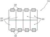
表达“矩阵”通常是指空间中的多个像素的排列,其可以是线性排列或面积排列。因此,通常,矩阵优选地可以选自包括一维矩阵和二维矩阵的组。矩阵的像素可以被布置成形成规则图案,其可以是矩形图案、多边形图案、六边形图案、圆形图案或另一种类型的图案中的至少一者。因此,作为示例,矩阵的像素可以在笛卡尔坐标系的每一个维度和/或极坐标系中等距地排列。作为示例,矩阵可以包括100到100000000个像素,优选地为1000到1000000个像素,更优选为10000到500000个像素。最优选地,矩阵是具有排列成行和列的像素的矩形矩阵。The expression "matrix" generally refers to an arrangement of a plurality of pixels in space, which may be a linear arrangement or an area arrangement. Thus, in general, the matrix may preferably be selected from the group consisting of one-dimensional matrices and two-dimensional matrices. The pixels of the matrix may be arranged to form a regular pattern, which may be at least one of a rectangular pattern, a polygonal pattern, a hexagonal pattern, a circular pattern, or another type of pattern. Thus, by way of example, the pixels of the matrix may be arranged equidistantly in each dimension of the Cartesian coordinate system and/or the polar coordinate system. As an example, the matrix may comprise 100 to 100000000 pixels, preferably 1000 to 1000000 pixels, more preferably 10000 to 500000 pixels. Most preferably, the matrix is a rectangular matrix with pixels arranged in rows and columns.
如下面进一步详细描述的,矩阵的像素可以相同或可以变化。因此,作为示例,矩阵的所有像素可以具有相同的光谱特性和/或可以具有相同的状态。作为示例,每一个像素可以具有导通状态和截止状态,其中处于导通状态的光可以穿过像素,或者可以由像素反射到经过的方向或光学传感器的方向,并且其中,在截止状态中,光由像素阻挡或衰减,或被反射到阻挡方向中,诸如远离光学传感器的束收集器(beam dump)。此外,像素可以具有不同的特性,诸如不同的状态。作为将在下面进一步详细描述的示例,像素可以是包括不同光谱特性(诸如关于光的透射波长和/或反射波长的不同过滤特性)的彩色像素。因此,作为示例,矩阵可以是具有红色、绿色和蓝色像素或具有不同颜色的其它类型的像素的矩阵。作为示例,SLM可以是全色SLM,诸如全色液晶装置和/或具有不同光谱特性的反射镜的微镜装置。As described in further detail below, the pixels of the matrix may be the same or may vary. Thus, by way of example, all pixels of the matrix may have the same spectral properties and/or may have the same state. As an example, each pixel may have an on state and an off state, wherein light in the on state may pass through the pixel, or may be reflected by the pixel to a passing direction or direction of the optical sensor, and wherein, in the off state, Light is blocked or attenuated by the pixel, or reflected into a blocking direction, such as a beam dump away from the optical sensor. Furthermore, pixels can have different characteristics, such as different states. As an example, which will be described in further detail below, a pixel may be a color pixel that includes different spectral properties, such as different filtering properties with respect to transmitted and/or reflected wavelengths of light. Thus, as an example, the matrix may be a matrix with red, green and blue pixels or other types of pixels with different colors. As an example, the SLM may be a panchromatic SLM, such as a panchromatic liquid crystal device and/or a micromirror device with mirrors of different spectral properties.
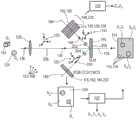
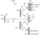
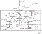
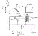
在本发明的另一方面,公开了一种光检测器。光学检测器包括:In another aspect of the invention, a photodetector is disclosed. Optical detectors include:
-根据上述调制器组件的至少一个调制器组件;- at least one modulator assembly according to the above-mentioned modulator assembly;
-至少一个光学传感器,其适用于检测通过所述空间光调制器的所述像素矩阵后的所述光束,并且适用于产生至少一个传感器信号;- at least one optical sensor adapted to detect said light beam after passing through said pixel matrix of said spatial light modulator and adapted to generate at least one sensor signal;
-适用于周期性地控制具有不同调制频率的至少两个像素的至少一个调制器装置;- at least one modulator device adapted to periodically control at least two pixels with different modulation frequencies;
-至少一个评估装置,其适用于进行频率分析,以便确定用于独特调制频率的所述传感器信号的信号分量。- at least one evaluation device adapted to perform a frequency analysis in order to determine the signal components of the sensor signal for unique modulation frequencies.
调制器组件包括根据本发明的调制器装置。关于限定和实施例,可以参考上面给出的方法和装置的限定和实施例,以及下面给出的装置的限定和实施例。The modulator assembly comprises a modulator device according to the present invention. With regard to definitions and examples, reference may be made to the definitions and examples of methods and apparatus given above, and the definitions and examples of apparatus given below.
如本文所使用的,“光学检测器”或在下文中简称为“检测器”通常是指能够产生至少一个检测器信号和/或至少一个图像的装置,其响应于一个或多个光源的照射和/或响应于检测器周围的光学性质。因此,检测器可以是适用于进行光学测量和成像处理中的至少一个的任意装置。As used herein, an "optical detector" or simply "detector" hereinafter generally refers to a device capable of producing at least one detector signal and/or at least one image in response to illumination and/or by one or more light sources. /or in response to optical properties around the detector. Thus, the detector may be any device suitable for performing at least one of optical measurement and imaging processing.
具体地,如下面将进一步详细描述的那样,光学检测器可以是用于确定至少一个对象的位置的检测器。如本文所使用的,术语位置通常是指关于对象和/或空间中对象的至少一部分的位置和/或取向的至少一个信息项。因此,至少一个信息项可以暗示对象的至少一个点与至少一个检测器之间的至少一个距离。如将在下面进一步详细描述的那样,距离可以是纵坐标,或者可以有助于确定对象的点的纵坐标。另外或替代地,可以确定关于对象和/或对象的至少一个部分的位置和/或取向的一个或多个其他信息项。作为示例,可以确定对象和/或对象的至少一个部分的至少一个横向坐标。因此,对象的位置可以暗示对象和/或对象的至少一部分的至少一个纵坐标。附加地或替代地,对象的位置可以暗示对象和/或对象的至少一部分的至少一个横向坐标。附加地或替代地,对象的位置可以暗示对象的指示对象在空间中的取向的至少一个取向信息。In particular, as will be described in further detail below, the optical detector may be a detector for determining the position of at least one object. As used herein, the term position generally refers to at least one item of information about the position and/or orientation of an object and/or at least a portion of an object in space. Thus, the at least one item of information may imply at least one distance between at least one point of the object and at least one detector. As will be described in further detail below, the distance can be an ordinate, or an ordinate of a point that can help determine the object. Additionally or alternatively, one or more other items of information regarding the position and/or orientation of the object and/or at least a portion of the object may be determined. As an example, at least one lateral coordinate of the object and/or at least a part of the object may be determined. Thus, the position of the object may imply at least one ordinate of the object and/or at least part of the object. Additionally or alternatively, the position of the object may imply at least one lateral coordinate of the object and/or at least part of the object. Additionally or alternatively, the position of the object may imply at least one orientation information of the object indicative of the orientation of the object in space.
如本文进一步使用的,术语“光学传感器”通常是指用于检测光束和/或其部分的诸如用于检测由光束产生的照射和/或光斑的光敏装置。结合评估装置的光学传感器可以如下面进一步详细描述的那样适应于确定对象和/或对象的至少一个部分(例如,这样的至少一个部分:至少一个光束从该至少一个部分朝向检测器传播)的至少一个纵坐标。As further used herein, the term "optical sensor" generally refers to a photosensitive device for detecting a light beam and/or a portion thereof, such as for detecting illumination and/or light spots produced by the light beam. The optical sensor in conjunction with the evaluation device may be adapted to determine at least the object and/or at least one part of the object (eg, the at least one part from which at least one light beam propagates towards the detector) as described in further detail below. an ordinate.
光学检测器可以包括一个或多个光学传感器。在包括多个光学传感器的情况下,光学传感器可以相同或可以不同(使得可以包括至少两种不同类型的光学传感器)。如下面进一步详细描述的,至少一个光学传感器可以包括无机光学传感器和有机光学传感器中的至少一个。如本文所用,有机光学传感器通常是指具有其中包含的至少一种有机材料的光学传感器,优选至少一种有机光敏材料。此外,可以使用包括无机和有机材料二者的混合光学传感器。The optical detector may include one or more optical sensors. Where multiple optical sensors are included, the optical sensors may be the same or may be different (so that at least two different types of optical sensors may be included). As described in further detail below, the at least one optical sensor may include at least one of an inorganic optical sensor and an organic optical sensor. As used herein, an organic optical sensor generally refers to an optical sensor having at least one organic material, preferably at least one organic photosensitive material, contained therein. In addition, hybrid optical sensors including both inorganic and organic materials can be used.
该至少一个光学传感器具体可以是或可以包括至少一个纵向光学传感器和/或至少一个横向光学传感器。对于术语“纵向光学传感器”和“横向光学传感器”的潜在限定以及这些传感器的潜在实施例,可以作为示例,参考如WO2014/097181A1所示的至少一个纵向光学传感器和/或至少一个横向光学传感器。其他设置是可行的。The at least one optical sensor may in particular be or may comprise at least one longitudinal optical sensor and/or at least one transverse optical sensor. For potential definitions of the terms "longitudinal optical sensor" and "transverse optical sensor" and potential embodiments of these sensors, reference may be made to at least one longitudinal optical sensor and/or at least one transverse optical sensor as shown in WO2014/097181A1. Other settings are possible.
至少一个光学传感器适用于在光束通过空间光调制器的像素矩阵之后,即在由空间光调制器传输和/或由空间光调制器反射之后检测光束。如本文所使用的,术语“检测”通常是指光学传感器适用于根据光束在光学传感器引导中的光束的至少一个性质产生至少一个传感器信号,优选地取决于光束的强度。然而,如下面将进一步详细描述的那样,传感器信号可以附加地或替代地取决于光束的其他性质,例如光束的宽度。传感器信号优选地可以是电信号,例如电流和/或电压。传感器信号优选地可以是电信号,诸如电流和/或电压。传感器信号可以是连续的或不连续的信号。此外,传感器信号可以是模拟信号或数字信号。此外,光学传感器本身和/或结合光学检测器的其它部件可以适于诸如通过滤波和/或平均来处理或预处理检测器信号,以便提供处理后的检测器信号。因此,作为示例,可以使用带通滤波器,以便仅发送特定频率范围的检测器信号。其它类型的预处理是可行的。在下面,当引用检测器信号时,在使用原始检测器信号的情况与预处理检测器信号用于进一步评估的情况之间将不会有差异。The at least one optical sensor is adapted to detect the light beam after it has passed through the pixel matrix of the spatial light modulator, ie after transmission by the spatial light modulator and/or reflection by the spatial light modulator. As used herein, the term "detection" generally refers to an optical sensor adapted to generate at least one sensor signal according to at least one property of the light beam in the optical sensor guidance, preferably depending on the intensity of the light beam. However, as will be described in further detail below, the sensor signal may additionally or alternatively depend on other properties of the beam, such as the width of the beam. The sensor signal may preferably be an electrical signal, such as current and/or voltage. The sensor signal may preferably be an electrical signal, such as current and/or voltage. The sensor signal can be a continuous or discontinuous signal. Furthermore, the sensor signal may be an analog signal or a digital signal. Furthermore, the optical sensor itself and/or other components in conjunction with the optical detector may be adapted to process or pre-process the detector signal, such as by filtering and/or averaging, to provide a processed detector signal. Thus, as an example, a bandpass filter can be used in order to transmit only detector signals of a certain frequency range. Other types of preprocessing are possible. In the following, when referring to the detector signal, there will be no difference between the case where the original detector signal is used and the case where the detector signal is preprocessed for further evaluation.
如本文进一步使用的,术语“评估装置”通常指适用于进行命名操作的任意装置。评估装置可以包含一个或多个子装置,诸如测量装置、频率分析器(优选相敏频率分析器)、傅里叶分析器、以及解调装置中的一者或多者。因此,作为示例,评估装置可以包括适于将特定调制频率与检测器信号相混合的至少一个频率混合装置。可以通过使用低通滤波器对以这种方式获得的混合信号进行滤波,以便获得解调后的信号。通过使用一组频率,可以由评估装置生成各种频率的解调信号,从而提供频率分析。频率分析可以是在频率或相位范围内的全频率分析,或者可以是用于一个、两个或更多个预定或可调频率和/或相位的选择性频率分析器。As further used herein, the term "evaluation device" generally refers to any device suitable for performing the named operation. The evaluation device may comprise one or more sub-devices, such as one or more of a measurement device, a frequency analyzer (preferably a phase sensitive frequency analyzer), a Fourier analyzer, and a demodulation device. Thus, by way of example, the evaluation device may comprise at least one frequency mixing device adapted to mix a specific modulation frequency with the detector signal. The mixed signal obtained in this way can be filtered by using a low-pass filter in order to obtain a demodulated signal. By using a set of frequencies, demodulated signals of various frequencies can be generated by the evaluation device, thereby providing frequency analysis. The frequency analysis may be a full frequency analysis in the frequency or phase range, or may be a selective frequency analyzer for one, two or more predetermined or tunable frequencies and/or phases.
如在此所使用的,术语“频率分析”通常是指评估装置可以适于以频率选择的方式评估检测器信号,从而将传感器信号的信号分量分离成至少两个不同的频率和/或相位(即根据它们的频率f和/或根据它们的相位

频率分析可以在一个、两个或更多个不同的频率处进行,从而在这些一个、两个或更多个不同的频率处获得传感器信号的信号分量。两个或更多个不同的频率可以是离散频率,或者可以是连续的频率范围,诸如频率间隔中的连续频率范围。频率分析仪通常在高频电子学领域中是已知的。The frequency analysis may be performed at one, two or more different frequencies to obtain signal components of the sensor signal at these one, two or more different frequencies. The two or more different frequencies may be discrete frequencies, or may be a continuous frequency range, such as a continuous frequency range in a frequency interval. Frequency analyzers are generally known in the field of high frequency electronics.
优选地,评估装置适用于对独特调制频率进行频率分析。因此,优选地,评估装置至少适于确定传感器信号的针对调制器装置所使用的不同独特调制频率的频率分量。事实上,调制器装置甚至可以完全地或部分地是评估装置的一部分,反之亦然。因此,作为示例,可以提供一个或多个信号发生器,其提供调制器装置所使用的独特调制频率和用于频率分析的频率。作为示例,所生成的至少一个信号可以用于提供一组独特调制频率,以便周期性地控制至少两个像素,优选更多或甚至所有像素,并且为频率分析提供一组相同的独特调制频率。因此,可以将该组独特调制频率的每一个独特调制频率提供给相应的像素。此外,可以将该组独特调制频率的每一个独特调制频率提供给评估装置的解调装置,以便用相应的独特调制频率解调传感器信号,从而获得相应独特调制频率的信号分量。因此,可以由评估装置生成一组信号分量,该组信号分量的每一个信号分量对应于该组独特调制频率的相应独特调制频率,并且因此对应于矩阵的相应像素。因此,优选地,评估装置可以适于在信号分量中的每一个信号分量和空间光调制器的像素矩阵的像素之间建立明确的相关性。换言之,评估装置可以适于将由至少一个光学传感器提供的传感器信号分离成由经过相应像素的光部分生成的信号分量和/或将信号分量分配给矩阵的特定像素。Preferably, the evaluation device is adapted for frequency analysis of the unique modulation frequency. Thus, preferably, the evaluation device is at least adapted to determine the frequency components of the sensor signal for the different unique modulation frequencies used by the modulator device. In fact, the modulator device may even be part of the evaluation device completely or partially, and vice versa. Thus, as an example, one or more signal generators may be provided that provide the unique modulation frequencies used by the modulator device and frequencies used for frequency analysis. As an example, the generated at least one signal may be used to provide a set of unique modulation frequencies to periodically control at least two pixels, preferably more or even all pixels, and to provide the same set of unique modulation frequencies for frequency analysis. Accordingly, each unique modulation frequency of the set of unique modulation frequencies may be provided to a corresponding pixel. Furthermore, each unique modulation frequency of the set of unique modulation frequencies can be provided to the demodulation means of the evaluation device in order to demodulate the sensor signal with the corresponding unique modulation frequency to obtain the signal component of the corresponding unique modulation frequency. Thus, a set of signal components can be generated by the evaluation device, each signal component of the set of signal components corresponding to a respective unique modulation frequency of the set of unique modulation frequencies, and thus corresponding pixels of the matrix. Thus, preferably, the evaluation means may be adapted to establish an unambiguous correlation between each of the signal components and the pixels of the pixel matrix of the spatial light modulator. In other words, the evaluation device may be adapted to separate the sensor signal provided by the at least one optical sensor into signal components generated by light sections passing through the respective pixels and/or to assign the signal components to specific pixels of the matrix.
在提供多个光学传感器的情况下,评估装置可以适于单独或共同地对光学传感器中的每一个光学传感器执行上述频率分析,或者可以适于仅对一个或多个光学传感器执行上述频率分析。Where a plurality of optical sensors are provided, the evaluation device may be adapted to perform the above-mentioned frequency analysis on each of the optical sensors individually or collectively, or may be adapted to perform the above-mentioned frequency analysis on only one or more optical sensors.
如将在下面进一步详细描述的,评估装置可以包括至少一个数据处理装置,诸如至少一个微控制器或处理器。因此,作为示例,至少一个评估装置可以包括至少一个数据处理装置,至少一个数据处理装置具有存储在其上的包括多个计算机命令的软件代码。另外或备选地,评估装置可以包括一个或多个电子部件,诸如一个或多个频率混合装置和/或一个或多个滤波器,诸如一个或多个带通滤波器和/或一个或多个低通滤波器。因此,作为示例,评估装置可以包括用于执行频率分析的至少一个傅立叶分析器和/或至少一个锁相放大器,或者优选地,一组锁相放大器。因此,作为示例,在提供一组调制频率的情况下,评估装置可以包括用于该组调制频率中的每个独特调制频率的单独的锁相放大器,或者可以包括适于诸如顺序地或同时地对于独特调制频率中的两个或更多个执行频率分析的一个或多个锁相放大器。该种锁相放大器通常在本领域中是已知的。As will be described in further detail below, the evaluation device may comprise at least one data processing device, such as at least one microcontroller or processor. Thus, by way of example, at least one evaluation device may comprise at least one data processing device having stored thereon software code comprising a plurality of computer commands. Additionally or alternatively, the evaluation device may comprise one or more electronic components, such as one or more frequency mixing devices and/or one or more filters, such as one or more bandpass filters and/or one or more a low-pass filter. Thus, as an example, the evaluation device may comprise at least one Fourier analyzer and/or at least one lock-in amplifier, or preferably a set of lock-in amplifiers, for performing frequency analysis. Thus, by way of example, where a set of modulation frequencies is provided, the evaluation means may comprise a separate lock-in amplifier for each unique modulation frequency in the set of modulation frequencies, or may comprise suitable One or more lock-in amplifiers that perform frequency analysis for two or more of the unique modulation frequencies. Such lock-in amplifiers are generally known in the art.
作为示例,评估装置可以包括适用于进行沃尔什分析的至少一个沃尔什分析器。因此,如本文所使用的,术语“沃尔什分析器”通常是指适用于或被配置为进行沃尔什分析的任意装置。作为示例,沃尔什分析器可以完全或部分地在软件和/或硬件中实现。此外,沃尔什分析器可以完全或部分地集成到或可以包括至少一个数据处理装置(诸如至少一个处理器和/或至少一个专用集成电路(ASIC))。沃尔什分析器可以完全或部分地集成到评估装置中和/或完全或部分地被实现到至少一个单独的装置中。As an example, the evaluation device may comprise at least one Walsh analyzer adapted to perform a Walsh analysis. Thus, as used herein, the term "Walsh analyzer" generally refers to any device suitable or configured to perform a Walsh analysis. As an example, a Walsh analyzer may be implemented in whole or in part in software and/or hardware. Furthermore, the Walsh analyzer may be fully or partially integrated into or may include at least one data processing device (such as at least one processor and/or at least one application specific integrated circuit (ASIC)). The Walsh analyzer can be fully or partially integrated into the evaluation device and/or fully or partially implemented into at least one separate device.
鉴于信号处理和信号处理装置,除傅里叶变换之外或者替代傅立叶变换,而使用沃尔什变换是特别有利的。沃尔什变换可以仅使用加法和减法处理来实现,而使用傅里叶变换,数字信号处理器可能需要以适用于处理浮点数。因此,当使用沃尔什变换时,可以使用与进行傅里叶变换所需的数字信号处理器相比较简单的数字信号处理器。因此,使用沃尔什函数和变换具体可能会带来成本效益。In view of signal processing and signal processing means, it is particularly advantageous to use the Walsh transform in addition to or instead of the Fourier transform. The Walsh transform can be implemented using only addition and subtraction processing, whereas using the Fourier transform, a digital signal processor may be required to be suitable for processing floating point numbers. Therefore, when the Walsh transform is used, a simpler digital signal processor can be used than that required to perform the Fourier transform. Therefore, it may be cost-effective to use the Walsh function and transform specifically.
频率分析的性能可能受噪声影响,使得噪声的存在可能导致重建误差,并且噪声可能会限制重建的质量。使用沃尔什变换,与使用傅里叶变换相比,可能会发生较低的重构误差。The performance of frequency analysis can be affected by noise, such that the presence of noise can lead to reconstruction errors, and noise can limit the quality of the reconstruction. Using the Walsh transform, a lower reconstruction error may occur compared to using the Fourier transform.
在进行频率分析之前,可以通过滤波处理来修改信号。因此,评估装置和/或沃尔什分析器可以包括至少一个滤波装置,该滤波装置适用于在进行频率分析之前对信号进行滤波。在信号(特别是由沃尔什函数组成的信号)在频率分析之前被滤波的情况下,沃尔什函数的系数可能受到影响。沃尔什函数可以分布在频域上,使得每个沃尔什函数的效果可能不同。对沃尔什系数的这种影响可以通过校准每个沃尔什系数,特别是通过振幅校准来考虑。校准过程可以在测量之前和/或期间进行。在对于每个沃尔什函数的第一校准步骤中,可以模拟具有和不应用滤波处理的重建,并且可以与原始沃尔什函数进行比较。在进一步的校准步骤中,可以调整沃尔什系数。可以重复进行校准过程,例如以提高重建质量。Before frequency analysis, the signal can be modified by a filtering process. Thus, the evaluation means and/or the Walsh analyser may comprise at least one filtering means adapted to filter the signal before performing the frequency analysis. The coefficients of the Walsh function may be affected in the case where the signal, especially one composed of Walsh functions, is filtered prior to frequency analysis. Walsh functions can be distributed in the frequency domain, so that the effect of each Walsh function may be different. This effect on the Walsh coefficients can be taken into account by calibrating each Walsh coefficient, in particular by amplitude calibration. The calibration process can be performed before and/or during the measurement. In a first calibration step for each Walsh function, the reconstruction with and without applied filtering processing can be simulated and compared to the original Walsh function. In a further calibration step, the Walsh coefficients can be adjusted. The calibration process can be repeated, for example, to improve reconstruction quality.
评估装置可以连接到或可以包括至少一个另外的数据处理装置,其可以用于信息(诸如由光学传感器和/或由评估装置获得的信息)的显示、可视化、分析、分发、通信或进一步处理中的一者或多者。作为示例,数据处理装置可以连接或并入显示器、投影仪、监视器、LCD、TFT、LED图案或另外的可视化装置中的至少一者。它可以进一步连接或并入能够使用电子邮件、文本消息、电话、蓝牙、Wi-Fi、红外线或互联网接口、端口或连接中的一个或多个发送加密或未加密信息的通信装置或通信接口、连接器或端口中的至少一个。作为示例,数据处理装置可以使用协议族或栈的通信协议来与评估装置或另一装置交换信息,其中通信协议具体可以是如下中的一个或多个:TCP、IP、UDP、FTP、HTTP、IMAP、POP3、ICMP、IIOP、RMI、DCOM、SOAP、DDE、NNTP、PPP、TLS、E6、NTP、SSL、SFTP、HTTPs、Telnet、SMTP、RTPS、ACL、SCO、L2CAP、RIP或另一协议。协议族或栈具体可以是TCP/IP、IPX/SPX、X.25、AX.25、OSI、AppleTalk或另一协议族或栈中的一种或多种。数据处理装置可以进一步连接或并入处理器、图形处理器、CPU、开放多媒体应用平台(OMAPTM)、集成电路、片上系统(诸如来自Apple A序列或三星S3C2序列的产品)、微控制器或微处理器、一个或多个存储器块(诸如ROM、RAM、EEPROM或闪存)、定时源(诸如振荡器或锁相环、计数计时器、实时定时器)或上电复位发生器、稳压器、电源管理电路或DMA控制器中的至少一者。各个单元可以进一步通过诸如AMBA总线的总线连接。The evaluation device may be connected to or may comprise at least one further data processing device, which may be used in the display, visualization, analysis, distribution, communication or further processing of information, such as information obtained by the optical sensor and/or by the evaluation device one or more of. As an example, the data processing device may be connected to or incorporated into at least one of a display, projector, monitor, LCD, TFT, LED pattern or further visualization device. It may further connect or incorporate a communication device or communication interface capable of sending encrypted or unencrypted information using one or more of email, text messaging, telephone, Bluetooth, Wi-Fi, infrared or internet interfaces, ports or connections, At least one of a connector or a port. As an example, the data processing device may exchange information with the evaluation device or another device using a communication protocol of a protocol suite or stack, wherein the communication protocol may specifically be one or more of the following: TCP, IP, UDP, FTP, HTTP, IMAP, POP3, ICMP, IIOP, RMI, DCOM, SOAP, DDE, NNTP, PPP, TLS, E6, NTP, SSL, SFTP, HTTPs, Telnet, SMTP, RTPS, ACL, SCO, L2CAP, RIP or another protocol. The protocol suite or stack may specifically be one or more of TCP/IP, IPX/SPX, X.25, AX.25, OSI, AppleTalk or another protocol suite or stack. The data processing device may be further connected to or incorporate a processor, graphics processor, CPU, Open Multimedia Application Platform (OMAP™ ), integrated circuit, system on chip (such as products from Apple A-series or Samsung S3C2-series), microcontrollers or Microprocessor, one or more memory blocks (such as ROM, RAM, EEPROM, or flash memory), timing sources (such as oscillators or phase-locked loops, counting timers, real-time timers) or power-on reset generators, voltage regulators , at least one of a power management circuit or a DMA controller. The individual units may further be connected by a bus such as an AMBA bus.
评估装置和/或数据处理装置可以通过另一外部接口或端口(诸如串行或并行接口或端口、USB、Centronics端口、FireWire、HDMI、以太网、蓝牙、RFID、Wi-Fi、USART或SPI,或诸如ADC或DAC中的一者或多者的模拟接口或端口,或标准化接口或端口中的一者或多者)连接至诸如使用诸如CameraLink的RGB接口的2D相机装置的另一装置,或具有另一外部接口或端口。评估装置和/或数据处理装置可以进一步通过处理器间接口或端口、FPGA-FPGA接口或串行或并行接口端口中的一者或多者来连接。评估装置和数据处理装置可以进一步连接到光盘驱动器、CD-RW驱动器、DVD+RW驱动器、闪存驱动器、存储卡、磁盘驱动器、硬盘驱动器、固态磁盘或固态硬盘中的一者或多者。The evaluation device and/or the data processing device can communicate via another external interface or port such as a serial or parallel interface or port, USB, Centronics port, FireWire, HDMI, Ethernet, Bluetooth, RFID, Wi-Fi, USART or SPI, or an analog interface or port such as one or more of an ADC or DAC, or one or more of a standardized interface or port) to another device such as a 2D camera device using an RGB interface such as CameraLink, or Has another external interface or port. The evaluation device and/or the data processing device may further be connected by one or more of an inter-processor interface or port, an FPGA-FPGA interface, or a serial or parallel interface port. The evaluation device and the data processing device may further be connected to one or more of an optical disk drive, CD-RW drive, DVD+RW drive, flash drive, memory card, magnetic disk drive, hard disk drive, solid state disk or solid state hard disk.
评估装置和/或数据处理装置可以由一个或多个另一外部连接器(诸如电话连接器、RCA连接器、VGA连接器、公母同体连接器、USB连接器、HDMI连接器、8P8C连接器、BCN连接器、IEC 60320 C14连接器、光纤连接器、D超小型连接器、RF连接器、同轴连接器、SCART连接器、XLR连接器中的一者或多者)连接或具有一个或多个另一外部连接器,和/或可以为这些连接器中的一个或多个并入至少一个合适的插座。The evaluation device and/or the data processing device may be connected by one or more other external connectors (such as telephone connectors, RCA connectors, VGA connectors, hermaphroditic connectors, USB connectors, HDMI connectors, 8P8C connectors , BCN connector, IEC 60320 C14 connector, fiber optic connector, D subminiature connector, RF connector, coaxial connector, SCART connector, one or more of XLR connector) connect or have one or A plurality of other external connectors, and/or at least one suitable socket may be incorporated for one or more of these connectors.
评估装置可以通过与调制装置的至少一个接口连接。因此,评估装置可以适用于接收和/或与调制器装置数据,该数据诸如为关于一组独特调制频率的信息和/或关于由调制器装置接收的至少一个图像的信息等。此外,评估装置可以连接到至少一个光学传感器(例如,包括CMOS芯片的光学传感器)和/或空间光调制器和/或一个或多个输出装置。The evaluation device can be connected via at least one interface to the modulation device. Thus, the evaluation device may be adapted to receive and/or communicate with the modulator device data, such as information on a unique set of modulation frequencies and/or information on at least one image received by the modulator device or the like. Furthermore, the evaluation device may be connected to at least one optical sensor (eg, an optical sensor comprising a CMOS chip) and/or a spatial light modulator and/or one or more output devices.
并入根据本发明的一个或多个光学检测器、评估装置或数据处理装置的单个装置(诸如并入光学传感器、光学系统、评估装置、通信装置、数据处理装置、接口、片上系统、显示装置或另一电子装置中的一个或多个)的可能实施例是:移动电话、个人计算机、平板电脑、电视机、游戏机或另一娱乐装置。在另一实施例中,将在下面进一步详细描述的3D相机功能可集成在用传统2D数字相机可获得的装置中,而在装置的壳体或外观上没有明显的差异,其中对于用户的明显的差异可能只是获取和/或处理3D信息的功能。A single device incorporating one or more optical detectors, evaluation devices or data processing devices according to the invention (such as incorporating an optical sensor, optical system, evaluation device, communication device, data processing device, interface, system on chip, display device or one or more of another electronic device) are: a mobile phone, a personal computer, a tablet, a television, a game console or another entertainment device. In another embodiment, the 3D camera functionality, which will be described in further detail below, may be integrated into a device obtainable with a conventional 2D digital camera without significant differences in the housing or appearance of the device, where it is apparent to the user The difference may simply be the function of acquiring and/or processing 3D information.
具体地,并入光学检测器和/或其一部分(诸如评估装置和/或数据处理装置)的实施例可以是:并入显示装置的移动电话、数据处理装置、光学传感器(可选地传感器光学器件)、以及评估装置,用于3D相机的功能。具体地,根据本发明的光学检测器可以适于集成在娱乐装置和/或诸如移动电话的通信装置中。In particular, embodiments incorporating an optical detector and/or a part thereof, such as an evaluation device and/or a data processing device, may be: a mobile phone incorporating a display device, a data processing device, an optical sensor (optionally a sensor optical device) device), and an evaluation device for the functionality of the 3D camera. In particular, the optical detector according to the present invention may be suitable for integration in entertainment devices and/or communication devices such as mobile phones.
本发明的另一实施例可以是光学检测器或其一部分(诸如评估装置和/或数据处理装置)在用于汽车、用于自主驾驶或用于诸如戴姆勒智能驾驶系统(Daimler’sIntelligent Drive system)的汽车安全系统的装置中的并入,其中,作为示例,并入光学传感器、可选地一个或多个光学系统、评估装置、可选地通信装置、可选地数据处理装置、可选地一个或多个接口、可选地片上系统、可选地一个或多个显示装置、或可选地另一电子装置中的一者或多者的装置可以是车辆、汽车、卡车、火车、自行车、飞机、船舶、摩托车的一部分。在汽车应用中,将装置集成到汽车设计中可能需要以从外部或内部看的最小可视性将光学传感器,可选的光学器件或装置集成。光学检测器或其一部分(诸如评估装置和/或数据处理装置)可以特别适用于到汽车设计中的这种集成。Another embodiment of the present invention may be an optical detector or a part thereof (such as an evaluation device and/or a data processing device) in use in automobiles, in autonomous driving or in systems such as Daimler's Intelligent Drive system), wherein, by way of example, an optical sensor, optionally one or more optical systems, an evaluation device, optionally a communication device, optionally a data processing device, an optional The device, optionally one or more of an interface, optionally a system on a chip, optionally one or more display devices, or optionally another electronic device, may be a vehicle, car, truck, train , part of bicycle, plane, ship, motorcycle. In automotive applications, integrating the device into an automotive design may require the integration of optical sensors, optional optics or devices with minimal visibility from the outside or inside. Optical detectors or parts thereof, such as evaluation devices and/or data processing devices, may be particularly suitable for such integration into automotive designs.
本发明基本上可以使用用于将频率分量分配给空间光调制器的特定像素的频率分析。通常,复杂的显示技术和具有高分辨率和/或高质量的合适的复杂空间光调制器以低成本广泛获得,而光学传感器的空间分辨率通常在技术上是具有挑战性的。因此,代替使用像素化光学传感器,本发明提供了可能使用大面积光学传感器或光学传感器的优点,该大面积光学传感器或光学传感器具有低分辨率,与像素化空间光调制器组合,结合经由频率分析分配传感器信号的信号分量给像素化空间光调制器的相应像素。因此,可以使用低成本的光学传感器,或者可以使用可以关于其它参数而不是诸如透明度、低噪声和高信号质量或颜色的分辨率来优化的光学传感器。由此施加的空间分辨率和技术挑战可以从光学传感器转移到空间光调制器。The present invention can basically use frequency analysis for assigning frequency components to specific pixels of a spatial light modulator. In general, sophisticated display technologies and suitable complex spatial light modulators with high resolution and/or high quality are widely available at low cost, while the spatial resolution of optical sensors is often technically challenging. Thus, instead of using a pixelated optical sensor, the present invention offers the advantage of possible use of a large area optical sensor or optical sensor with low resolution, in combination with a pixelated spatial light modulator, in combination with frequency The analysis assigns the signal components of the sensor signal to corresponding pixels of the pixelated spatial light modulator. Thus, low-cost optical sensors can be used, or optical sensors that can be optimized with respect to other parameters than resolution such as transparency, low noise and high signal quality or color can be used. The spatial resolution and technical challenges thus imposed can be transferred from optical sensors to spatial light modulators.
至少一个空间光调制器可进一步适于和/或被控制以提供一个或多个光图案。因此,至少一个空间光调制器可以被控制成使得一个或多个光图案朝向至少一个光学传感器(诸如朝向至少一个纵向光学传感器)反射和/或传输。至少一个光图案通常可以是或可以包括至少一个通用光图案和/或可以是或可以包括至少一个光图案,该至少一个光图案取决于由光学检测器捕获的空间或场景和/或可以取决于由光学检测器捕获的场景的特定分析。通用图案的示例是:基于条纹的图案(参见例如T.Peng:“用于使用数字边缘投影的三维形状测量的算法和模型”,马里兰大学(College Park,Md.),2007年1月16日-可在http://drum.lib.umd.edu//handle/1903/6654处获得)和/或基于灰度码的图案(参见例如http://en.wikipedia.org/wiki/Gray_code)。这些类型的图案通常用于基于结构化光照射的3D识别(参见例如http://en.wikipedia.org/wiki/Structured-light_3D_scanner)或边缘投影)。The at least one spatial light modulator may be further adapted and/or controlled to provide one or more light patterns. Accordingly, the at least one spatial light modulator may be controlled such that one or more light patterns are reflected and/or transmitted towards the at least one optical sensor, such as towards the at least one longitudinal optical sensor. The at least one light pattern generally can be or can include at least one general light pattern and/or can be or can include at least one light pattern that depends on the space or scene captured by the optical detector and/or can depend on Specific analysis of the scene captured by the optical detector. Examples of common patterns are: stripe-based patterns (see e.g. T. Peng: "Algorithms and Models for Three-Dimensional Shape Measurement Using Digital Edge Projection", University of Maryland (College Park, Md.), January 16, 2007 - available at http://drum.lib.umd.edu//handle/1903/6654) and/or gray-code based patterns (see e.g. http://en.wikipedia.org/wiki/Gray_code) . These types of patterns are commonly used for 3D recognition based on structured light illumination (see eg http://en.wikipedia.org/wiki/Structured-light_3D_scanner) or edge projection).
空间光调制器和光学传感器可以在空间上分离,诸如通过将这些部件建立为光学检测器的单独部件。作为示例,沿着光学检测器的光轴,空间光调制器可以与至少一个光学传感器分离至少0.5mm,优选地至少1mm,并且更优选地至少2mm。然而,其它实施例是可行的,诸如通过将空间光调制器完全或部分地集成到光学传感器中。The spatial light modulator and optical sensor can be spatially separated, such as by establishing these components as separate components of the optical detector. As an example, along the optical axis of the optical detector, the spatial light modulator may be separated from the at least one optical sensor by at least 0.5 mm, preferably at least 1 mm, and more preferably at least 2 mm. However, other embodiments are possible, such as by fully or partially integrating the spatial light modulator into the optical sensor.
根据本发明的该基本原理的光学检测器可以通过可以单独或以任何可行的组合使用的各种实施例来进一步开发。Optical detectors according to this basic principle of the invention can be further developed by various embodiments which can be used alone or in any feasible combination.
因此,如上所述,评估装置可以进一步适于根据信号分量的独特调制频率将每一个信号分量分配给相应的像素。对于进一步的细节,可以参考上面给出的实施例。因此,作为示例,可以使用一组独特调制频率,每一个独特调制频率被分配给矩阵的特定像素,其中评估装置可以适于至少针对独特调制频率组的独特调制频率执行传感器信号的频率分析,从而至少针对这些独特调制频率导出信号分量。如上所述,相同的信号发生器可以用于调制器装置和用于频率分析二者。优选地,调制器装置可以适于使得像素中的每一个像素以独特调制频率来控制。因此,通过使用独特调制频率,可以建立调制频率和相应像素之间明确定义的关系,以使得每一个信号分量可以经由独特调制频率分配给相应的像素。其它实施例仍是可行的,诸如通过将光学传感器和/或空间光调制器细分成两个或更多个区域。其中,空间光调制器的每一个区域与光学传感器和/或其一部分相结合可以适于执行上述分配。因此,作为示例,可以将该组调制频率提供给空间光调制器的第一区域和空间光调制器的至少一个第二区域。从第一区域生成的传感器信号和从第二区域生成的传感器信号之间的传感器信号的信号分量中的不确定性可以通过其它手段(诸如通过使用附加调制)来解决。Thus, as described above, the evaluation device may be further adapted to assign each signal component to a corresponding pixel according to its unique modulation frequency. For further details, reference may be made to the examples given above. Thus, as an example, a set of unique modulation frequencies can be used, each unique modulation frequency being assigned to a specific pixel of the matrix, wherein the evaluation means can be adapted to perform a frequency analysis of the sensor signal at least for the unique modulation frequencies of the unique set of modulation frequencies, thereby Signal components are derived for at least these unique modulation frequencies. As mentioned above, the same signal generator can be used for both the modulator device and for the frequency analysis. Preferably, the modulator means may be adapted such that each of the pixels is controlled with a unique modulation frequency. Thus, by using a unique modulation frequency, a well-defined relationship between the modulation frequency and the corresponding pixel can be established such that each signal component can be assigned to the corresponding pixel via the unique modulation frequency. Other embodiments are still possible, such as by subdividing the optical sensor and/or spatial light modulator into two or more regions. Therein, each area of the spatial light modulator in combination with an optical sensor and/or a part thereof may be adapted to perform the above assignment. Thus, as an example, the set of modulation frequencies may be provided to the first region of the spatial light modulator and to at least one second region of the spatial light modulator. The uncertainty in the signal component of the sensor signal between the sensor signal generated from the first region and the sensor signal generated from the second region can be resolved by other means, such as by using additional modulation.
因此,通常,调制器装置可以适于控制至少两个像素,优选更多的像素,甚至是矩阵的所有像素,每一个像素具有精确的一个独特调制频率或者每一个像素具有两个或更多个独特调制频率。因此,可以用一个独特调制频率、两个独特调制频率或更多的独特调制频率来调制单个像素。这些类型的多频调制通常在高频电子学领域中是已知的。Thus, in general, the modulator device may be adapted to control at least two pixels, preferably more pixels, or even all pixels of a matrix, each pixel having exactly one unique modulation frequency or each pixel having two or more Unique modulation frequency. Thus, a single pixel can be modulated with one unique modulation frequency, two unique modulation frequencies, or more. These types of multi-frequency modulations are generally known in the field of high frequency electronics.
如上所述,调制器装置可适于以不同独特调制频率周期性地调制至少两个像素。更优选地,如上所讨论,调制器装置可以提供或可以利用一组独特调制频率,该组独特调制频率的每一个独特调制频率被分配给特定像素。作为示例,该组独特调制频率可以包括至少两个独特调制频率,更优选至少五个独特调制频率,最优选至少10个独特调制频率,至少50个独特调制频率,至少100个独特调制频率,至少500个独特调制频率或至少1000个独特调制频率。其它实施例是可行的。As mentioned above, the modulator means may be adapted to periodically modulate the at least two pixels at different unique modulation frequencies. More preferably, as discussed above, the modulator device may provide or may utilize a set of unique modulation frequencies, each of which is assigned to a particular pixel. As an example, the set of unique modulation frequencies may include at least two unique modulation frequencies, more preferably at least five unique modulation frequencies, most preferably at least 10 unique modulation frequencies, at least 50 unique modulation frequencies, at least 100 unique modulation frequencies, at least 500 unique modulation frequencies or at least 1000 unique modulation frequencies. Other embodiments are possible.
如上面更详细所述的,评估装置优选地可以适于通过用不同的独特调制频率解调传感器信号来执行频率分析。为此,评估装置可以包含一个或多个解调装置,诸如一个或多个频率混合装置、一个或多个频率滤波器,诸如一个或多个低通滤波器或一个或多个锁相放大器和/或傅里叶分析器。评估装置优选地可以适于在预定和/或可调节的频率范围上执行离散或连续的傅里叶分析。此外,评估装置优选地可以包括适用于进行沃尔什分析的至少一个沃尔什分析器。As described in more detail above, the evaluation device may preferably be adapted to perform frequency analysis by demodulating the sensor signal with different unique modulation frequencies. For this purpose, the evaluation device may comprise one or more demodulation devices, such as one or more frequency mixing devices, one or more frequency filters, such as one or more low-pass filters or one or more lock-in amplifiers and / or Fourier analyzer. The evaluation device may preferably be adapted to perform discrete or continuous Fourier analysis over a predetermined and/or adjustable frequency range. Furthermore, the evaluation means may preferably comprise at least one Walsh analyzer adapted to perform a Walsh analysis.
如上所讨论,评估装置优选地可以适于使用同样由调制器装置使用的相同的一组独特调制频率,以使得调制器装置对空间光调制器的调制和评估装置对传感器信号的解调优选地以一组相同的独特调制频率发生。As discussed above, the evaluation device may preferably be adapted to use the same set of unique modulation frequencies also used by the modulator device, so that modulation of the spatial light modulator by the modulator device and demodulation of the sensor signal by the evaluation device preferably Occurs at the same set of unique modulation frequencies.
进一步的优选实施例涉及由空间光调制器以空间分辨的方式修改的光束的至少一个特性,优选至少一个光学特性。因此,优选地,由空间光调制器以空间分辨的方式修改的光束的至少一个特性是选自以下组的至少一个特性:光束部分的强度;光束部分的相位;光束部分的光谱特性,优选为颜色;光束部分的极化;光束部分的传播方向。作为示例,如上所述,对于每一个像素,空间光调制器可以适于导通或截止经过该相应像素的光部分,即适于在第一状态和第二状态之间切换,在第一状态中光的一部分可以朝向光学传感器行进,并且在第二状态中防止光的该部分朝向光学传感器行进。其它选项仍是可行的,诸如在具有像素的第一透射的第一状态和具有不同于第一透射的像素的第二透射的第二状态之间的强度调制。其它选项是可行的。A further preferred embodiment relates to at least one property, preferably at least one optical property, of the light beam being modified by the spatial light modulator in a spatially resolved manner. Thus, preferably, the at least one characteristic of the light beam modified by the spatial light modulator in a spatially resolved manner is at least one characteristic selected from the group consisting of: intensity of the beam portion; phase of the beam portion; spectral characteristic of the beam portion, preferably Color; polarization of the beam part; propagation direction of the beam part. As an example, as described above, for each pixel, the spatial light modulator may be adapted to switch on or off the portion of the light passing through that respective pixel, ie to switch between a first state and a second state, in the first state A portion of the light may travel towards the optical sensor, and the portion of the light is prevented from travelling towards the optical sensor in the second state. Other options are still possible, such as intensity modulation between a first state with a first transmission of the pixel and a second state with a second transmission of the pixel different from the first transmission. Other options are possible.
优选地,至少一个空间光调制器可以包括选自以下组的至少一个空间光调制器:基于液晶技术的空间光调制器,诸如一个或多个液晶空间光调制器;基于微机械系统的空间光调制器,诸如基于微镜系统(具体是微镜阵列)的空间光调制器;基于干涉调制的空间光调制器;基于声光效应的空间光调制器;基于电光效应的空间光调制器,具体地基于普克尔效应和/或克尔效应;透射空间光调制器,其中光束穿过像素矩阵,并且其中像素适于以单独可控的方式修改穿过相应像素的光束的每一个部分的光学特性;反射空间光调制器,其中像素具有独立可控的反射特性,并且适于单独地改变由相应像素反射的光束的每一个部分的传播方向;透射空间光调制器,其中像素具有单独可控的反射特性,并且适于通过控制分配给相应像素的微镜的位置来单独地改变每一个像素的透射;基于干涉式调制的空间光调制器,其中光束穿过像素矩阵,并且其中像素适于通过修改像素的干涉效应来修改穿过相应像素的光束的每一个部分的光学特性;电致变色空间光调制器,其中像素具有由施加到相应像素的电压可单独控制的可控光谱特性;声光空间光调制器,其中像素的双折射可由声波控制;电光空间光调制器,其中像素的双折射可由电场控制,优选地基于普克尔效应和/或克尔效应的空间光调制器;包括可调光学元件的至少一个阵列(诸如可调焦透镜阵列、自适应液体微透镜的区域、透明微棱镜阵列中的一者或多者)的空间光调制器。这些类型的空间光调制器通常是本领域技术人员已知的,并且至少部分地是可商购的。因此,作为示例,至少一个空间光调制器可以包括选自以下组的至少一个空间光调制器:液晶装置,优选有源矩阵液晶器件,其中像素是单独可控的液晶装置单元;微镜装置,其中像素是微镜装置的微镜,其可关于微镜反射表面的取向单独可控;电致变色装置,其中像素是电致变色装置的单元,其具有通过施加到相应单元的电压单独控制的光谱特性;声光装置,其中像素是声光装置的单元,其具有通过施加到单元的声波可单独控制的双折射;电光装置,其中像素是电光装置的单元,其具有通过施加到单元的电场可单独控制的双折射。两种或多种命名技术的组合是可行的。微镜装置通常可商购,诸如实现所谓的
如上所述,像素修改光束的至少一个特性的能力在像素矩阵上可以是均匀的。备选地,像素修改至少一个特性的能力可以在像素之间不同,以使得像素矩阵的至少一个第一像素具有修改特性的第一能力,以及像素矩阵的至少一个第二像素具有修改特性的第二能力。此外,可以通过像素修改光束的多于一个的特性。再次,像素可以能够修改光束的相同特性或光束的不同类型的特性。因此,作为示例,至少一个第一像素可以适于修改光束的第一特性,并且至少一个第二像素可以适于修改不同于光束的第一特性的光束的第二特性。此外,像素修改通过相应像素的光束的一部分的至少一个光学特性的能力可以取决于光束的光谱特性,具体是光束的颜色。因此,作为示例,像素修改光束的至少一个特性的能力可以取决于光束的波长和/或光束的颜色,其中术语“颜色”通常指光束强度的光谱分布。再次,像素可以具有均匀的特性或不同的特性。因此,作为示例,至少一个第一像素或至少一个第一像素组可以具有在蓝色光谱范围中具有高透射率的滤光特性,第二组像素可具有在红色光谱范围中具有高透射率的滤光特性,并且第三组像素可以具有在绿色光谱范围中具有高透射率的滤光特性。通常,可以存在针对具有不同透射范围的光束的滤波特性的至少两组像素,其中每一组内的像素另外可以在至少一个低透射状态和至少一个高透射状态之间切换。其它实施例是可行的。As described above, the ability of the pixels to modify at least one characteristic of the light beam may be uniform across the pixel matrix. Alternatively, the ability of the pixels to modify at least one characteristic may differ from pixel to pixel such that at least one first pixel of the pixel matrix has the first ability to modify the characteristic and at least one second pixel of the pixel matrix has the first ability to modify the characteristic. Second ability. Furthermore, more than one characteristic of the light beam can be modified by the pixel. Again, a pixel may be able to modify the same characteristic of the light beam or a different type of characteristic of the light beam. Thus, by way of example, at least one first pixel may be adapted to modify a first characteristic of the light beam and at least one second pixel may be adapted to modify a second characteristic of the light beam different from the first characteristic of the light beam. Furthermore, the ability of a pixel to modify at least one optical property of a portion of the light beam passing through the corresponding pixel may depend on the spectral properties of the light beam, in particular the color of the light beam. Thus, as an example, the ability of a pixel to modify at least one characteristic of a light beam may depend on the wavelength of the light beam and/or the color of the light beam, where the term "color" generally refers to the spectral distribution of the light beam intensity. Again, pixels can have uniform characteristics or different characteristics. Thus, as an example, at least one first pixel or at least one first group of pixels may have a filter characteristic with high transmittance in the blue spectral range, and the second group of pixels may have a high transmittance in the red spectral range filter characteristics, and the third group of pixels may have filter characteristics with high transmittance in the green spectral range. Typically, there may be at least two groups of pixels with filtering characteristics for beams with different transmission ranges, wherein the pixels within each group may additionally be switchable between at least one low transmission state and at least one high transmission state. Other embodiments are possible.
如上所述,空间光调制器可以是透明的空间光调制器或非透明的空间光调制器。在后者情况下,优选地,空间光调制器是诸如具有多个微镜的微镜装置的反射空间光调制器,每一个微镜形成微镜装置的像素,其中每一个微镜可以在至少两个取向之间单独切换。因此,作为示例,每一个微镜的第一取向可以是其中通过微镜的光束部分(即入射在微镜上)被导向光学传感器的取向,并且第二取向可以是其中通过微镜的光束部分(即入射在微镜上)的取向被导向另一方向并且不到达光学传感器(例如通过被引导到一个束收集器)的取向。As mentioned above, the spatial light modulator may be a transparent spatial light modulator or a non-transparent spatial light modulator. In the latter case, preferably, the spatial light modulator is a reflective spatial light modulator such as a micromirror arrangement with a plurality of micromirrors, each micromirror forming a pixel of the micromirror arrangement, wherein each micromirror can be in at least Toggle between the two orientations individually. Thus, as an example, the first orientation of each micromirror may be the orientation in which the portion of the beam passing through the micromirror (ie incident on the micromirror) is directed towards the optical sensor, and the second orientation may be the portion of the beam passing through the micromirror The orientation (ie incident on the micromirror) is directed in the other direction and does not reach the orientation of the optical sensor (eg by being directed to a beam dump).
另外或备选地,空间光调制器可以是透射空间光调制器,优选地是其中像素的透射率可以切换(优选地,单独切换)的透射空间光调制器。因此,作为示例,空间光调制器可以包括至少一个透明液晶装置,诸如广泛用于投影目的的液晶装置,例如,用于演示目的的投影机。液晶装置可以是具有相同光谱特性的像素的单色液晶装置,或者可以是具有不同光谱特性像素(诸如红绿色和蓝色像素)的多色或甚至全色液晶装置。Additionally or alternatively, the spatial light modulator may be a transmissive spatial light modulator, preferably a transmissive spatial light modulator in which the transmittance of the pixels can be switched (preferably individually switched). Thus, as an example, the spatial light modulator may comprise at least one transparent liquid crystal device, such as liquid crystal devices widely used for projection purposes, eg, projectors for presentation purposes. The liquid crystal device may be a monochromatic liquid crystal device having pixels with the same spectral properties, or a polychromatic or even panchromatic liquid crystal device having pixels with different spectral properties, such as red-green and blue pixels.
如上所述,评估装置优选地适于将信号分量中的每一个信号分量分配给矩阵的像素。评估装置可以进一步适于通过评估信号分量来确定由光束照射矩阵的哪些像素。因此,由于每一个信号分量可以经由唯一的相关性对应于特定像素,所以光谱分量的评估可以导致对像素的照射的评估。作为示例,评估装置可以适于将信号分量与至少一个阈值进行比较,以便确定被照射像素。该至少一个阈值可以是固定阈值或预定阈值,或者可以是可变或可调阈值。作为示例,可以选择高于信号分量的典型噪声的预定阈值,并且在相应像素的信号分量超过阈值的情况下,可以确定像素的照射。至少一个阈值可以是所有信号分量的统一阈值,或者可以是相应信号分量的个体阈值。因此,在不同的信号分量倾向于示出不同程度的噪声的情况下,可以选择个体阈值以便考虑这些个体噪声。As mentioned above, the evaluation device is preferably adapted to assign each of the signal components to the pixels of the matrix. The evaluation device may be further adapted to determine which pixels of the matrix are illuminated by the light beam by evaluating the signal components. Thus, since each signal component can correspond to a particular pixel via a unique correlation, an evaluation of the spectral components can lead to an evaluation of the illumination of the pixel. As an example, the evaluation device may be adapted to compare the signal component with at least one threshold value in order to determine the illuminated pixel. The at least one threshold may be a fixed threshold or a predetermined threshold, or may be a variable or adjustable threshold. As an example, a predetermined threshold value above the typical noise of the signal component may be chosen, and in case the signal component of the corresponding pixel exceeds the threshold value, the illumination of the pixel may be determined. The at least one threshold may be a uniform threshold for all signal components, or may be an individual threshold for the respective signal components. Thus, where different signal components tend to show different degrees of noise, individual thresholds can be chosen to take these individual noises into account.
评估装置可以进一步适于通过识别由光束照明的矩阵像素的横向位置来识别光束的至少一个横向位置和/或光束的取向,诸如相对于检测器的光轴的取向。因此,作为示例,可以通过评估信号分量识别具有最高照明的至少一个像素,来识别像素矩阵上的光束的中心。具有最高照明的至少一个像素可以位于矩阵的特定位置处,然后再次将该特定位置识别为光束的横向位置。在这方面,通常,可以参考欧洲专利申请号EP 13171901.5中公开的确定光束的横向位置的原理,尽管其它选项是可行的。The evaluation device may be further adapted to identify at least one lateral position of the light beam and/or an orientation of the light beam, such as an orientation relative to the optical axis of the detector, by identifying the lateral position of the matrix pixels illuminated by the light beam. Thus, as an example, the center of the light beam on the pixel matrix can be identified by evaluating the signal components to identify at least one pixel with the highest illumination. At least one pixel with the highest illumination can be located at a specific position of the matrix, which is then again identified as a lateral position of the beam. In this regard, in general, reference can be made to the principles of determining the lateral position of the beam disclosed in European Patent Application No. EP 13171901.5, although other options are possible.
通常,如以下将使用的,可以定义检测器的几个方向。因此,可以在坐标系中定义对象的位置和/或取向,该坐标系优选地可以是检测器的坐标系。因此,检测器可以构成如下坐标系,在该坐标系中检测器的光轴形成z轴,并且另外可以提供垂直于z轴并且彼此垂直的x轴和y轴。作为示例,检测器和/或检测器的一部分可以停留在该坐标系中的特定点处,诸如在该坐标系的原点。在该坐标系中,与z轴平行或反平行的方向可以被认为是纵向方向,并且沿z轴的坐标可以被认为是纵坐标。垂直于纵向方向的任意方向可以被认为是横向方向,并且x和/或y坐标可以被认为是横坐标。In general, as will be used below, several orientations of the detector can be defined. Thus, the position and/or orientation of the object may be defined in a coordinate system, which may preferably be the detector's coordinate system. Thus, the detector may constitute a coordinate system in which the optical axis of the detector forms the z-axis, and additionally an x-axis and a y-axis may be provided which are perpendicular to the z-axis and to each other. As an example, a detector and/or a portion of a detector may rest at a particular point in the coordinate system, such as at the origin of the coordinate system. In this coordinate system, a direction parallel or anti-parallel to the z-axis can be considered a longitudinal direction, and a coordinate along the z-axis can be considered an ordinate. Any direction that is perpendicular to the longitudinal direction may be considered to be the transverse direction, and the x and/or y coordinates may be considered the abscissa.
备选地,可以使用其它类型的坐标系。因此,作为示例,可以使用极坐标系,其中光轴形成z轴,并且其中距z轴的距离和极角可用作附加坐标。再次,与z轴平行或反平行的方向可以被认为是纵向方向,并且沿z轴的坐标可以被认为是纵坐标。垂直于z轴的任何方向可以被认为是横向方向,并且极坐标和/或极角可以被认为是横坐标。Alternatively, other types of coordinate systems may be used. Thus, as an example, a polar coordinate system may be used, where the optical axis forms the z-axis, and where the distance from the z-axis and the polar angle may be used as additional coordinates. Again, directions parallel or anti-parallel to the z-axis may be considered longitudinal directions, and coordinates along the z-axis may be considered ordinates. Any direction perpendicular to the z-axis can be considered a transverse direction, and polar coordinates and/or polar angles can be considered abscissas.
可以以各种方式使用像素矩阵上的光束的中心,其可以是光束在像素矩阵上的中心点或中心区。因此,可以确定用于光束中心的至少一个横坐标,其在下面同样将被称为光束中心的xy坐标。The center of the light beam on the pixel matrix can be used in various ways, which can be the central point or central area of the light beam on the pixel matrix. Thus, at least one abscissa for the center of the beam can be determined, which will also be referred to below as the xy coordinate of the center of the beam.
此外,光束中心的位置可以允许获得与朝向检测器传播的光束所源自的对象的横向位置和/或相对方向有关的信息。因此,由光束照明的矩阵的像素的横向位置通过确定具有通过光束的最高照明的一个或多个像素来确定。为此目的,可以使用检测器的已知成像特性。作为示例,从对象向检测器传播的光束可以直接入射在特定区域上,并且从该区域的位置或者特别地从光束的中心的位置,可以导出对象的横向位置和/或方向。可选地,检测器可以包括具有光学特性的至少一个传送装置,诸如至少一个透镜或透镜系统。通常,由于传送装置的光学特性是已知的,诸如通过使用已知的成像方程和/或从射线光学或矩阵光学已知的几何关系,因此在使用一个或多个传送装置的情况下光束在像素矩阵上的中心位置同样可以用于导出关于对象的横向位置的信息。因此,通常,通过评估光束的横向位置和光束的取向中的至少一个,评估装置可以适于识别朝向检测器传播的光束所源自的对象的横向位置以及朝向检测器传播的光束所源自的对象的相对方向中的一个或多个。在这方面,作为示例,同样可以参考一个或多个横向光学传感器,如欧洲专利申请号EP13171901.5、美国临时申请号61/739,173或美国临时申请号61/749964中的一个或多个所公开的。然而,其它选项是可行的。Furthermore, the position of the beam center may allow obtaining information about the lateral position and/or relative orientation of the object from which the beam propagating towards the detector originates. Thus, the lateral position of the pixels of the matrix illuminated by the beam is determined by determining the pixel or pixels with the highest illumination by the beam. For this purpose, known imaging properties of the detector can be used. As an example, a beam propagating from an object to a detector may be directly incident on a certain area, and from the position of this area, or in particular from the position of the center of the beam, the lateral position and/or orientation of the object may be derived. Optionally, the detector may comprise at least one transfer device having optical properties, such as at least one lens or lens system. Typically, where one or more delivery devices are used, the beam is in the The center position on the pixel matrix can also be used to derive information about the lateral position of the object. Thus, in general, by evaluating at least one of the lateral position of the light beam and the orientation of the light beam, the evaluation device may be adapted to identify the lateral position of the object from which the light beam propagating towards the detector originates and from which the light beam propagating towards the detector originates. One or more of the relative orientation of the object. In this regard, by way of example, reference may also be made to one or more lateral optical sensors, as disclosed in one or more of European Patent Application No. EP13171901.5, US Provisional Application No. 61/739,173 or US Provisional Application No. 61/749964 of. However, other options are possible.
通过进一步评估光谱分析的结果,具体地通过评估信号分量,评估装置可以进一步适于导出与光束有关和/或与光束从其朝向检测器传播的对象的位置有关的一项或多项其它信息。因此,作为示例,评估装置可以适于导出选自以下组的一项或多项信息:光束从其朝向检测器传播的对象的位置;光束在空间光调制器的像素矩阵上的横向位置;光束在空间光调制器的像素矩阵的位置处的宽度;光束的颜色和/或光束的光谱特性;光束从其朝向检测器传播的对象的纵坐标。以下将更详细地给出这些信息项的示例和导出这些信息项。By further evaluating the results of the spectral analysis, in particular by evaluating the signal components, the evaluation device may be further adapted to derive one or more other information about the light beam and/or about the position of the object from which the light beam propagates towards the detector. Thus, by way of example, the evaluation device may be adapted to derive one or more pieces of information selected from the group consisting of: the position of the object from which the light beam propagates towards the detector; the lateral position of the light beam on the pixel matrix of the spatial light modulator; the light beam The width at the location of the pixel matrix of the spatial light modulator; the color of the light beam and/or the spectral properties of the light beam; the ordinate of the object from which the light beam propagates towards the detector. Examples of these items of information and derivation of these items of information will be given in more detail below.
因此,作为示例,评估装置可以适于通过评估信号分量来确定光束的宽度。通常,如在本文所使用的,术语“光束的宽度”是指由光束在像素矩阵上生成的照明光斑的(具体地在垂直于光束的传播的局部方向(诸如上面提及的z轴)的平面中的)横向扩展的任意量度。因此,作为示例,光束的宽度可以通过提供光斑的面积、光斑直径、光斑的等效直径、光斑的半径或者光斑的等效半径中的一个或多个来指定。作为示例,可以指定所谓的束腰,以便确定光束在空间光传感器的位置处的宽度,如下面将进一步详细描述的。具体地,评估装置可以适于识别分配给由光束照明的像素的信号分量,并从像素布置的已知几何特性确定在空间光传感器位置处的光束的宽度。因此,具体地,在矩阵的像素位于矩阵的已知位置的情况下,其通常是这种情况,通过频率分析导出的相应像素的信号分量可以变换为由光束对空间光传感器的照明的空间分布,从而能够导出关于在空间光传感器的位置处的光束的宽度的至少一项信息。Thus, as an example, the evaluation device may be adapted to determine the width of the light beam by evaluating the signal components. Generally, as used herein, the term "width of the beam" refers to the width of the illumination spot generated by the beam on the pixel matrix (specifically in a local direction perpendicular to the beam's propagation, such as the above-mentioned z-axis) in a plane) any measure of lateral expansion. Thus, by way of example, the width of the beam may be specified by providing one or more of the area of the spot, the diameter of the spot, the equivalent diameter of the spot, the radius of the spot, or the equivalent radius of the spot. As an example, a so-called beam waist may be specified in order to determine the width of the beam at the location of the spatial light sensor, as will be described in further detail below. In particular, the evaluation device may be adapted to identify the signal components assigned to the pixels illuminated by the light beam and to determine the width of the light beam at the location of the spatial light sensor from known geometrical properties of the pixel arrangement. Thus, in particular, where the pixels of the matrix are located at known positions of the matrix, which is often the case, the signal components of the corresponding pixels, derived by frequency analysis, can be transformed into the spatial distribution of the illumination of the spatial light sensor by the beam of light , so that at least one item of information about the width of the light beam at the location of the spatial light sensor can be derived.
在已知光束的宽度的情况下,该宽度可以用于导出关于光束从其朝向检测器行进的对象的位置的一项或多项信息。因此,使用光束的宽度与光束从其朝向检测器传播的对象和检测器之间的距离之间的已知或可确定的关系,评估装置可以适于确定对象的纵坐标。对于通过评估光束的宽度来导出对象的纵坐标的一般原理,可以参考WO 2012/110924A1、EP 13171901.5、US临时申请号61/739,173或美国临时申请号61/749964中的一个或多个。Where the width of the beam is known, this width can be used to derive one or more pieces of information about the position of the object from which the beam travels towards the detector. Thus, using a known or determinable relationship between the width of the beam and the distance between the object from which the beam propagates towards the detector and the detector, the evaluation device may be adapted to determine the ordinate of the object. For the general principle of deriving the ordinate of an object by evaluating the width of the beam, reference may be made to one or more of WO 2012/110924 A1, EP 13171901.5, US Provisional Application No. 61/739,173 or US Provisional Application No. 61/749964.
因此,作为示例,评估装置可以适于对像素中的每一个将相应像素的信号分量与至少一个阈值比较,以便确定像素是否是被照明像素。该至少一个阈值可以是用于像素中的每一个的个体阈值,或者可以是用于整个矩阵的统一阈值的阈值。如上所述,阈值可以是预定的和/或固定的。备选地,该至少一个阈值可以是可变的。因此,可以对于每一个测量或每一组测量单独确定至少一个阈值。因此,可以提供适于确定阈值的至少一个算法。Thus, by way of example, the evaluation means may be adapted to compare, for each of the pixels, the signal component of the respective pixel with at least one threshold in order to determine whether the pixel is an illuminated pixel. The at least one threshold may be an individual threshold for each of the pixels, or may be a uniform threshold for the entire matrix. As mentioned above, the threshold may be predetermined and/or fixed. Alternatively, the at least one threshold may be variable. Thus, at least one threshold may be determined individually for each measurement or each group of measurements. Accordingly, at least one algorithm suitable for determining the threshold may be provided.
评估装置通常可以适于通过比较像素的信号来确定像素中具有最高照明的至少一个像素。因此,检测器通常可以适于确定具有由光束的最高照明强度的一个或多个像素和/或矩阵的面积或区域。作为示例,以这种方式,可以确定由光束照明的中心。The evaluation device may generally be adapted to determine at least one of the pixels with the highest illumination by comparing the signals of the pixels. Thus, the detector may generally be adapted to determine the area or area of one or more pixels and/or matrices having the highest illumination intensity by the light beam. As an example, in this way the center illuminated by the light beam can be determined.
可以以各种方式使用最高照明和/或关于最高照明的至少一个面积或区域的信息。因此,如上所述,至少一个上述阈值可以是可变阈值。作为示例,评估装置可以适于选择上述至少一个阈值作为具有最高照明的至少一个像素的信号的分数。因此,评估装置可以适于通过将具有最高照明的至少一个像素的信号乘以因子1/e2来选择阈值。如下面将进一步详细描述的,对于至少一个光束,假设高斯传播特性的情况是特别优选的,因为阈值1/e2通常确定在光学传感器上由高斯光束生成的具有束半径或束腰w的光斑的边界。The highest illumination and/or the information about at least one area or area of highest illumination may be used in various ways. Thus, as described above, at least one of the aforementioned thresholds may be a variable threshold. As an example, the evaluation device may be adapted to select the above-mentioned at least one threshold as the fraction of the signal of the at least one pixel with the highest illumination. Thus, the evaluation device may be adapted to select the threshold value by multiplying the signal of the at least one pixel with the highest illumination by a
评估装置可以适于通过使用光束的宽度或者与其相当的由光束照明的像素的数量N与对象的纵坐标之间的预定关系来确定对象的纵坐标。因此,通常,由于传播特性对本领域技术人员通常是已知的,光束的直径随着传播(诸如随着传播的纵坐标)而变化。照明像素的数量与对象的纵坐标之间的关系可以是经验确定的关系和/或可以分析地确定。The evaluation device may be adapted to determine the ordinate of the object by using a predetermined relationship between the width of the light beam, or its equivalent, the number N of pixels illuminated by the light beam, and the ordinate of the object. Thus, generally, the diameter of the beam varies with propagation, such as with the ordinate of the propagation, as the propagation characteristics are generally known to those skilled in the art. The relationship between the number of illuminated pixels and the ordinate of the object may be an empirically determined relationship and/or may be determined analytically.
因此,作为示例,校准处理可用于确定光束的宽度和/或照明像素的数量与纵坐标之间的关系。另外或备选地,如上所述,该预定关系可以基于光束是高斯光束的假设。光束可以是具有精确的一个波长λ的单色光束,或者可以是具有多个波长或一个波长光谱的光束,其中,作为示例,光谱的中心波长和/或光谱的特征峰波长可以被选择为光束的波长λ。Thus, as an example, a calibration process may be used to determine the relationship between the width of the beam and/or the number of illuminated pixels and the ordinate. Additionally or alternatively, as described above, the predetermined relationship may be based on the assumption that the beam is a Gaussian beam. The light beam may be a monochromatic light beam with exactly one wavelength λ, or may be a light beam with multiple wavelengths or a spectrum of wavelengths, wherein, by way of example, the central wavelength of the spectrum and/or the characteristic peak wavelength of the spectrum may be selected as the beam wavelength λ.
作为分析确定的关系的示例,可以通过假设光束的高斯特性导出的预定关系可以是:As an example of an analytically determined relationship, a predetermined relationship that can be derived by assuming Gaussian properties of the beam can be:

其中z是纵坐标,where z is the ordinate,
其中wu是当在空间中传播时光束的最小光束半径,where wu is the minimum beam radius of the beam when propagating in space,
其中z0是光束的瑞利长度,
该关系通常可以从沿着坐标系的z轴行进的高斯光束的强度I的一般方程导出,其中r是垂直于z轴的坐标,并且E是光束的电场:This relationship can generally be derived from the general equation for the intensity I of a Gaussian beam traveling along the z-axis of the coordinate system, where r is the coordinate perpendicular to the z-axis, and E is the electric field of the beam:

对于特定的z值,通常表示高斯曲线的高斯光束的横向轮廓的束半径w被定义为距z轴的特定距离,在该特定距离处,幅度E已经降至为1/e(约36%)的值并且强度I已经降至1/e2。在上述给出的高斯方程中(同样可能出现在其它z值处,例如当执行z坐标变换时)在坐标z=0处出现的最小束半径由w0表示。取决于z坐标,当光束沿着z轴传播时,束半径通常遵循以下方程:For a specific value of z, the beam radius w of the lateral profile of a Gaussian beam, usually representing a Gaussian curve, is defined as the specific distance from the z-axis at which the amplitude E has dropped to 1/e (about 36%) and the intensity I has dropped to 1/e2. In the Gaussian equation given above (which may also occur at other z-values, eg when performing a z-coordinate transformation), the smallest beam radius that occurs at coordinate z=0 is denoted by w0 . Depending on the z-coordinate, when the beam propagates along the z-axis, the beam radius generally follows the equation:

被照射像素的数量N与光学传感器的被照射面积A成比例:The number N of illuminated pixels is proportional to the illuminated area A of the optical sensor:
N~A (4)N~A (4)
或者在使用多个空间光调制器i=1,...,n的情况下,对于每一个光学传感器,被照射像素的数量Ni与相应空间光调制器的被照射面积Ai成比例Or in the case of using multiple spatial light modulators i=1, . . . , n, for each optical sensor, the numberNi of illuminated pixels is proportional to the illuminated area A iof the corresponding spatial light modulator
Ni~Ai (4')Ni ~Ai (4')
并且具有半径w的圆的一般面积:And the general area of a circle with radius w:
A=π·w2, (5)A=π·w2 , (5)
可以导出被照射像素的数量和z坐标之间的以下关系:The following relationship between the number of illuminated pixels and the z-coordinate can be derived:

或
相应地,为
在上面给出的方程中,诸如在方程(1)中,假设光束在位置z=0处具有聚焦。然而,应当注意,z坐标的坐标变换是可能的,诸如通过加上和/或减去特定值。因此,作为示例,聚焦的位置通常取决于对象距检测器的距离和/或光束的其它特性。因此,通过确定聚焦和/或聚焦的位置,诸如通过使用聚焦的位置与对象和/或信标装置的纵坐标之间的经验和/或分析关系,可以确定对象的位置,具体是对象的纵坐标。In the equations given above, such as in equation (1), the beam is assumed to have focus at position z=0. However, it should be noted that a coordinate transformation of the z-coordinate is possible, such as by adding and/or subtracting certain values. Thus, by way of example, the location of focus typically depends on the distance of the object from the detector and/or other characteristics of the beam. Thus, by determining the focus and/or the position of focus, such as by using an empirical and/or analytical relationship between the position of focus and the ordinate of the object and/or beacon device, the position of the object, in particular the longitudinal direction of the object, can be determined coordinate.
此外,可以考虑至少一个可选传送装置(诸如至少一个可选透镜)的成像特性。因此,作为示例,在从对象朝向检测器引导的光束的束特性已知的情况下,诸如在包含在信标装置中的照明装置的发射特性已知的情况下,通过使用表示从对象到传送装置的传播、表示传送装置的成像并且表示从传送装置到至少一个光学传感器的束传播的适当的高斯转换矩阵,束腰与对象和/或信标装置的位置之间的相关性可以很容易地分析确定。另外或可替代地,相关性可以通过适当的校准测量来凭经验地确定。Furthermore, imaging characteristics of at least one optional delivery device, such as at least one optional lens, may be considered. Thus, by way of example, where the beam properties of the light beam directed from the object towards the detector are known, such as where the emission properties of the lighting device contained in the beacon device are known, the transmission from the object to the The propagation of the device, an appropriate Gaussian transformation matrix representing the imaging of the delivery device and representing the beam propagation from the delivery device to the at least one optical sensor, the correlation between the beam waist and the position of the object and/or the beacon device can easily be Analysis confirmed. Additionally or alternatively, the correlation may be determined empirically by appropriate calibration measurements.
如上所述,像素矩阵优选地可以是二维矩阵。然而,其它实施例是可行的,诸如一维矩阵。更优选地,如上所述,像素矩阵是矩形矩阵,特别是方形矩阵。As mentioned above, the pixel matrix may preferably be a two-dimensional matrix. However, other embodiments are possible, such as a one-dimensional matrix. More preferably, as mentioned above, the pixel matrix is a rectangular matrix, in particular a square matrix.
如上所述,通过频率分析导出的信息可以进一步用于导出关于对象和/或光束的其它类型的信息。作为可以另外或备选地导出到横向和/或纵向位置信息的信息的另一示例,可以命名对象和/或光束的颜色和/或光谱特性。As described above, the information derived by the frequency analysis can be further used to derive other types of information about the object and/or the light beam. As another example of information that may additionally or alternatively be derived to lateral and/or longitudinal position information, the color and/or spectral properties of objects and/or light beams may be named.
因此,像素修改通过相应像素的光束部分的至少一个光学特性的能力可以取决于光束的光谱性质,具体地取决于光束的颜色。评估装置具体可以适于将信号分量分配给具有不同光谱特性的光束的分量。因此,作为示例,可以将一个或多个第一信号分量分配给适于在第一光谱范围中发射或反射光束部分的一个或多个像素,一个或多个第二信号分量可分配给适于在第二光谱范围中发射或反射光束部分的一个或多个像素,以及一个或多个第三信号分量可分配给适于在第三光谱范围中发射或反射光束部分的一个或多个像素。因此,像素矩阵可以具有至少两个的具有不同光谱特性的不同的像素组,并且评估装置可以适于区分这些组的信号分量,从而允许光束的完整或部分光谱分析。作为示例,矩阵可以具有红色、绿色和蓝色像素,其每一个可以被个体地控制,并且评估装置可以适于将信号分量分配给所述组中的一个。例如,全色液晶SLM可用于该目的。Thus, the ability of a pixel to modify at least one optical property of the portion of the light beam passing through the corresponding pixel may depend on the spectral properties of the light beam, in particular on the color of the light beam. The evaluation device may in particular be adapted to assign the signal components to the components of the light beam having different spectral properties. Thus, by way of example, one or more first signal components may be assigned to one or more pixels adapted to emit or reflect portions of the beam in the first spectral range, and one or more second signal components may be assigned to One or more pixels emitting or reflecting beam portions in the second spectral range, and one or more third signal components may be assigned to one or more pixels adapted to emit or reflect beam portions in the third spectral range. Thus, the pixel matrix may have at least two different groups of pixels with different spectral properties, and the evaluation device may be adapted to distinguish the signal components of these groups, thereby allowing full or partial spectral analysis of the light beam. As an example, the matrix may have red, green and blue pixels, each of which may be controlled individually, and the evaluation device may be adapted to assign a signal component to one of the groups. For example, full-color liquid crystal SLMs can be used for this purpose.
因此,通常,评估装置可以适于通过比较分配给具有不同光谱特性的光束的分量(具体地分配给具有不同波长的光束的分量)的信号分量来确定光束的颜色。像素矩阵可以包括具有不同光谱特性(优选地具有不同的颜色)的像素,其中评估装置可以适于将信号分量分配给具有不同光谱特性的相应像素。调制器装置可以适于以与具有第二颜色的像素不同的方式来控制具有第一颜色的像素。Thus, in general, the evaluation device may be adapted to determine the colour of the light beam by comparing the signal components of the components assigned to the light beams with different spectral properties, in particular the components assigned to the light beams with different wavelengths. The pixel matrix may comprise pixels with different spectral properties (preferably with different colors), wherein the evaluation means may be adapted to assign signal components to corresponding pixels with different spectral properties. The modulator means may be adapted to control the pixels of the first colour differently than the pixels of the second colour.
如上所述,本发明的优点之一在于可以避免光学传感器的精细像素化的事实。相反,可以使用像素化SLM,从而实际上将像素化从实际光学传感器转移到SLM。具体地,至少一个光学传感器可以是或可以包括至少一个大面积光学传感器,其适于检测穿过多个像素的光束的多个部分。因此,至少一个光学传感器可以提供适于提供整体传感器信号的单个非分段整体传感器区域,其中至少对于进入检测器并通过平行于光轴的SLM或光学传感器中的一个或两个的光束,传感器区域适于检测通穿成像装置的光束的所有部分。作为示例,整体传感器区域可以具有至少25mm2,优选至少100mm2,以及更优选至少400mm2的敏感区。其它实施例仍是可行的,诸如具有两个或更多个传感器区域的实施例。此外,在使用两个或更多个光学传感器的情况下,光学传感器不一定必须相同。因此,一个或多个大面积光学传感器可以与一个或多个像素化光学传感器组合,诸如与一个或多个相机芯片(例如一个或多个CCD或CMOS芯片)组合,如下面将进一步详细描述的。As mentioned above, one of the advantages of the present invention lies in the fact that fine pixelation of the optical sensor can be avoided. Instead, a pixelated SLM can be used, effectively transferring the pixelation from the actual optical sensor to the SLM. In particular, the at least one optical sensor may be or may comprise at least one large area optical sensor adapted to detect portions of a light beam passing through a plurality of pixels. Thus, at least one optical sensor may provide a single non-segmented integral sensor area adapted to provide an integral sensor signal, wherein at least for light beams entering the detector and passing through one or both of the SLM or the optical sensor parallel to the optical axis, the sensor The zone is adapted to detect all parts of the light beam passing through the imaging device. As an example, the overall sensor area may have a sensitive area of at least 25 mm2 , preferably at least 100 mm2 , and more preferably at least 400 mm2 . Other embodiments are still possible, such as embodiments with two or more sensor areas. Furthermore, where two or more optical sensors are used, the optical sensors do not necessarily have to be the same. Thus, one or more large area optical sensors may be combined with one or more pixelated optical sensors, such as with one or more camera chips (eg, one or more CCD or CMOS chips), as will be described in further detail below .
至少一个光学传感器或者(在提供多个光学传感器的情况下)光学传感器中的至少一个优选地可以是完全或部分透明的。因此,通常,至少一个光学传感器可以包括至少一个至少部分透明的光学传感器,以使光束至少部分地可以穿过母体光学传感器。如在本文所使用的,术语“至少部分透明”可以指整个光学传感器是透明的或光学传感器的一部分(诸如敏感区域)是透明的选项,和/或光学传感器或光学传感器的至少透明部分可以以衰减或非衰减的方式透射光束的选项。因此,作为示例,透明光学传感器可以具有至少10%,优选至少20%,至少40%,至少50%或至少70%的透明度。透明度可以取决于光束的波长,并且给定的透明度可以对于在红外光谱范围、可见光谱范围和紫外光谱范围中的至少一个中的至少一个波长是有效的。通常,如在本文所使用的,红外光谱范围是指780nm至1mm的范围,优选为780nm至50μm的范围,更优选为780nm至3.0μm的范围。可见光谱范围是指380nm至780nm的范围。其中,包括紫色光谱范围的蓝色光谱范围可以被限定为380nm至490nm,其中纯蓝色光谱范围可以限定为430nm至490nm。包括黄色光谱范围的绿色光谱范围可以限定为490nm至600nm,其中纯绿色光谱范围可以限定为490nm至470nm。包括橙色光谱范围的红色光谱范围可以限定为600nm至780nm,其中纯红色光谱范围可以限定为640nm至780nm。紫外光谱范围可以限定为1nm至380nm,优选为50nm至380nm,更优选为200nm至380nm。The at least one optical sensor or (where a plurality of optical sensors are provided) at least one of the optical sensors may preferably be fully or partially transparent. Thus, typically, the at least one optical sensor may comprise at least one optical sensor that is at least partially transparent, so that the light beam may pass at least partially through the parent optical sensor. As used herein, the term "at least partially transparent" may refer to the option that the entire optical sensor is transparent or a portion of the optical sensor (such as a sensitive area) is transparent, and/or the optical sensor or at least a transparent portion of the optical sensor may be transparent Option to transmit the beam in an attenuated or non-attenuated manner. Thus, by way of example, the transparent optical sensor may have a transparency of at least 10%, preferably at least 20%, at least 40%, at least 50% or at least 70%. The transparency may depend on the wavelength of the light beam, and a given transparency may be effective for at least one wavelength in at least one of the infrared spectral range, the visible spectral range, and the ultraviolet spectral range. Generally, as used herein, the infrared spectral range refers to the range of 780 nm to 1 mm, preferably the range of 780 nm to 50 μm, more preferably the range of 780 nm to 3.0 μm. The visible spectral range refers to the range from 380 nm to 780 nm. Therein, the blue spectral range including the violet spectral range may be defined as 380 nm to 490 nm, wherein the pure blue spectral range may be defined as 430 nm to 490 nm. The green spectral range, including the yellow spectral range, may be defined as 490 nm to 600 nm, wherein the pure green spectral range may be defined as 490 nm to 470 nm. The red spectral range, including the orange spectral range, may be defined as 600 nm to 780 nm, wherein the pure red spectral range may be defined as 640 nm to 780 nm. The UV spectral range can be defined as 1 nm to 380 nm, preferably 50 nm to 380 nm, more preferably 200 nm to 380 nm.
为了提供感觉效应,通常,光学传感器通常必须在光束和光学传感器之间提供一些种类的相互作用,这通常导致透明度的损失。光学传感器的透明度可以取决于光束的波长,导致光学传感器的灵敏度、吸收或透明度的光谱分布。如上所述,在提供多个光学传感器的情况下,光学传感器的光谱特性不一定必须相同。因此,光学传感器中的一个可以在红色光谱区域中提供强吸收(诸如吸光率峰、吸收率峰或吸收峰中的一个或多个),光学传感器中的另一个可以在绿色光谱区域中提供强吸收,并且另一个可以在蓝色光谱区域中提供强吸收。其它实施例是可行的。In order to provide a sensory effect, the optical sensor typically has to provide some kind of interaction between the light beam and the optical sensor, which often results in a loss of transparency. The transparency of an optical sensor may depend on the wavelength of the light beam, resulting in a spectral distribution of sensitivity, absorption or transparency of the optical sensor. As described above, in the case where a plurality of optical sensors are provided, the spectral characteristics of the optical sensors do not necessarily have to be the same. Thus, one of the optical sensors can provide strong absorption (such as one or more of an absorbance peak, absorptivity peak, or absorption peaks) in the red spectral region, and the other of the optical sensors can provide strong absorption in the green spectral region absorption, and the other can provide strong absorption in the blue spectral region. Other embodiments are possible.
如上所述,在提供多个光学传感器的情况下,光学传感器可以形成堆叠。因此,至少一个光学传感器包括至少两个光学传感器的堆叠。堆叠的光学传感器中的至少一个可以是至少部分透明的光学传感器。因此,优选地,光学传感器的堆叠可以包括至少一个至少部分透明的光学传感器和可以是透明或非透明的至少一个另一光学传感器。优选地,提供至少两个透明光学传感器。具体地,距离空间光调制器最远的一侧的光学传感器同样可以是非透明的光学传感器,诸如非透明传感器,其中可以使用有机或无机光学传感器,诸如像CCD或CMOS芯片的无机半导体传感器。As mentioned above, where a plurality of optical sensors are provided, the optical sensors may form a stack. Thus, the at least one optical sensor comprises a stack of at least two optical sensors. At least one of the stacked optical sensors may be an at least partially transparent optical sensor. Thus, preferably, the stack of optical sensors may comprise at least one optical sensor, which is at least partially transparent, and at least one further optical sensor, which may be transparent or non-transparent. Preferably, at least two transparent optical sensors are provided. In particular, the optical sensor on the side farthest from the spatial light modulator can also be a non-transparent optical sensor, such as a non-transparent sensor, wherein organic or inorganic optical sensors can be used, such as inorganic semiconductor sensors like CCD or CMOS chips.
堆叠可以部分地或完全地浸入油和/或液体中以避免和/或减少接口处的反射。因此,堆叠的至少一个光学传感器可以完全或部分地浸入油和/或液体中。The stack may be partially or fully immersed in oil and/or liquid to avoid and/or reduce reflections at the interface. Thus, the stacked at least one optical sensor can be fully or partially immersed in oil and/or liquid.
如上所述,至少一个光学传感器须是像素化的光学传感器。因此,通过使用执行频率分析的一般思想,可以省略像素化。然而,具体地,在提供多个光学传感器的情况下,可以使用一个或多个像素化的光学传感器。因此,具体地,在使用光学传感器的堆叠的情况下,堆叠的光学传感器中的至少一个可以是具有多个光敏像素的像素化光学传感器。作为示例,像素化光学传感器可以是像素化的有机和/或无机光学传感器。最优选地,特别是由于它们的商业可用性,像素化光学传感器可以是无机像素化光学传感器,优选CCD芯片或CMOS芯片。因此,作为示例,堆叠可以包括一个或多个透明的大面积非像素化光学传感器,诸如一个或多个DSC,且更优选地是sDSC(如将在下面进一步详细描述的);以及至少一个无机像素化光学传感器,诸如CCD芯片或CMOS芯片。作为示例,至少一个无机像素化光学传感器可以位于堆叠的离空间光调制器最远的一侧上。具体地,像素化光学传感器可以是相机芯片,且更优选地是全色相机芯片。通常,像素化光学传感器可以是颜色敏感的,即可以是适于诸如通过提供具有不同的颜色灵敏度的至少两种不同类型的像素,更优选地至少三种不同类型的像素,来区分光束的颜色分量的像素化光学传感器。因此,作为示例,像素化光学传感器可以是全色成像传感器。As mentioned above, at least one optical sensor must be a pixelated optical sensor. Therefore, by using the general idea of performing frequency analysis, pixelation can be omitted. However, in particular where multiple optical sensors are provided, one or more pixelated optical sensors may be used. Thus, in particular, where a stack of optical sensors is used, at least one of the stacked optical sensors may be a pixelated optical sensor having a plurality of photosensitive pixels. As an example, a pixelated optical sensor may be a pixelated organic and/or inorganic optical sensor. Most preferably, especially due to their commercial availability, the pixelated optical sensors may be inorganic pixelated optical sensors, preferably CCD chips or CMOS chips. Thus, by way of example, the stack may include one or more transparent large area non-pixilated optical sensors, such as one or more DSCs, and more preferably sDSCs (as will be described in further detail below); and at least one inorganic Pixelated optical sensors, such as CCD chips or CMOS chips. As an example, at least one inorganic pixelated optical sensor may be located on the side of the stack furthest from the spatial light modulator. In particular, the pixelated optical sensor may be a camera chip, and more preferably a full-color camera chip. Typically, a pixelated optical sensor may be colour sensitive, ie may be adapted to distinguish the colour of a light beam, such as by providing at least two different types of pixels, more preferably at least three different types of pixels with different colour sensitivities Component pixelated optical sensor. Thus, as an example, the pixelated optical sensor may be a full-color imaging sensor.
优选地,至少一个光学传感器包含至少一个纵向光学传感器,即适用于确定至少一个对象的纵向位置(诸如对象的至少一个z坐标)的光学传感器。优选地,光学传感器或者在提供多个光学传感器的情况下至少一个光学传感器,可以具有如WO 2012/110924 A1中所公开的光学传感器的设置和/或功能。因此,优选地,至少一个光学传感器和/或一个或多个光学传感器可以具有至少一个传感器区域(region),其中光学传感器的传感器信号取决于光束对传感器区域的照射,其中给定相同的照射总功率,传感器信号取决于传感器区域中的光束的几何形状(特别是宽度),其中评估装置适用于通过评估传感器信号来确定宽度。在下文中,这种效果通常被称为FiP效应,因为给定相同的照射总功率p,传感器信号i取决于光子的通量F,即每单位面积的光子数。然而,应当注意,基于FiP效应的检测器仅仅是纵向光学传感器的优选实施例。附加地或替代地,可以使用一种或多种其它类型的纵向光学传感器。因此,在下文中,在参考FiP传感器的情况下,应注意,通常可以使用其他类型的纵向光学传感器。然而,由于FiP传感器的优异的性能和由于其优点,优选使用至少一个FiP传感器。Preferably, the at least one optical sensor comprises at least one longitudinal optical sensor, ie an optical sensor suitable for determining a longitudinal position of at least one object, such as at least one z-coordinate of the object. Preferably, the optical sensor, or at least one optical sensor where a plurality of optical sensors are provided, may have the arrangement and/or function of an optical sensor as disclosed in WO 2012/110924 A1. Thus, preferably, at least one optical sensor and/or one or more optical sensors may have at least one sensor region, wherein the sensor signal of the optical sensor depends on the illumination of the sensor region by the light beam, wherein given the same illumination total The power, the sensor signal depends on the geometry (in particular the width) of the beam in the sensor area, wherein the evaluation device is adapted to determine the width by evaluating the sensor signal. In the following, this effect is often referred to as the FiP effect, because given the same total illumination power p, the sensor signal i depends on the flux F of photons, ie the number of photons per unit area. However, it should be noted that detectors based on the FiP effect are only preferred embodiments of longitudinal optical sensors. Additionally or alternatively, one or more other types of longitudinal optical sensors may be used. Therefore, in the following, with reference to the FiP sensor, it should be noted that other types of longitudinal optical sensors can generally be used. However, due to the excellent performance of the FiP sensor and due to its advantages, it is preferred to use at least one FiP sensor.
在美国临时申请61/739173和61/749964中进一步公开的FiP效应可用于确定光束从其朝向检测器行进的对象的纵向位置。因此,由于其在传感器区域(优选地可以是非像素化的传感器区域)上的光束取决于光束的宽度(例如直径或半径,其也取决于检测器和对象之间的距离),传感器信号可以用于确定对象的纵坐标。因此,作为示例,评估装置可以适用于使用对象的纵坐标和传感器信号之间的预定关系,以便确定纵坐标。可以通过使用经验校准测量和/或通过使用已知的波束传播性质(例如高斯波束传播性质)来导出预定关系。详情可参考WO 2012/110924 A1和/或美国临时申请61/739,173和61/749,964。The FiP effect, further disclosed in US Provisional Applications 61/739173 and 61/749964, can be used to determine the longitudinal position of the object from which the beam travels towards the detector. Thus, since its beam on the sensor area (which may preferably be a non-pixelated sensor area) depends on the width of the beam (eg diameter or radius, which also depends on the distance between the detector and the object), the sensor signal can be used with to determine the ordinate of the object. Thus, as an example, the evaluation device may be adapted to use a predetermined relationship between the ordinate of the object and the sensor signal in order to determine the ordinate. The predetermined relationship can be derived by using empirical calibration measurements and/or by using known beam propagation properties (eg Gaussian beam propagation properties). Details can be found in WO 2012/110924 A1 and/or US Provisional Applications 61/739,173 and 61/749,964.
优选地,在提供多个光学传感器的情况下,例如光学传感器的堆叠,至少两个光学传感器可以适用于提供FiP效应。具体地说,可以提供呈现出FiP效应的一个或多个光学传感器,其中优选地,呈现FiP效应的光学传感器是具有均匀的传感器表面的大面积的光学传感器而不是像素化的光学传感器。Preferably, where multiple optical sensors are provided, eg a stack of optical sensors, at least two optical sensors may be adapted to provide the FiP effect. In particular, one or more optical sensors may be provided that exhibit the FiP effect, wherein preferably the optical sensor exhibiting the FiP effect is a large area optical sensor with a uniform sensor surface rather than a pixelated optical sensor.
因此,通过评估随后被光束照射的光学传感器的信号,例如传感器堆叠的后续光学传感器,并且通过使用上述FiP效应,可以解决光束轮廓中的模糊性。因此,高斯光束可以在焦点之前和之后的距离z处提供相同的光束宽度。通过沿着至少两个位置测量波束宽度,可以通过确定光束是否变窄或变宽来解决该模糊性。因此,通过提供具有FiP效应的两个或更多个光学传感器,可以提供更高的精度。评估装置可以适用于确定至少两个光学传感器的传感器区域中的光束的宽度,并且评估装置还可以适用于通过评估宽度在对象的纵向位置上产生至少一个信息项,光束从该对象而向光学检测器传播。Thus, by evaluating the signal of an optical sensor that is subsequently illuminated by the beam, eg a subsequent optical sensor of a sensor stack, and by using the FiP effect described above, the ambiguity in the beam profile can be resolved. Therefore, a Gaussian beam can provide the same beam width at distance z before and after the focus. By measuring the beam width along at least two locations, this ambiguity can be resolved by determining whether the beam narrows or widens. Therefore, by providing two or more optical sensors with FiP effect, higher accuracy can be provided. The evaluation device may be adapted to determine the width of the light beam in the sensor area of the at least two optical sensors, and the evaluation device may also be adapted to generate, by evaluating the width, at least one item of information in the longitudinal position of the object from which the light beam is directed toward the optical detection device spread.
具体地,在至少一个光学传感器或一个或多个光学传感器提供上述FiP效应的情况下,光学传感器的传感器信号可以取决于光束的调制频率。作为示例,FiP效应可以用作0.1Hz至10kHz的调制频率。In particular, where at least one optical sensor or one or more optical sensors provide the above-mentioned FiP effect, the sensor signal of the optical sensor may depend on the modulation frequency of the light beam. As an example, the FiP effect can be used as a modulation frequency of 0.1 Hz to 10 kHz.
因此,通常,光束可以由一个或多个调制装置调制。用于增强和/或实现FiP效应的调制可以是与控制空间光调制器的像素的调制器装置使用的调制相同的调制和/或可以是不同的调制。因此,空间光调制器可以提供使得能够和/或增强FiP效应的调制。附加地或替代地,可以提供附加的调制,例如通过使用一个或多个适用于以调制的方式发射光束的照射源。因此,作为示例,调制器装置使用的调制和空间光调制器的像素可以处于第一频率范围,例如在1Hz至100Hz的范围内,而另外,光束本身可以可选地另外由至少一个第二调制频率调制,例如在100Hz至10kHz的第二频率范围内的频率。第一频率范围的其他示例可以是100至500Hz或100至1000Hz。第二频率范围的其它示例可以是500Hz至10kHz或1000Hz至10kHz。低于100Hz的滤波可能有利于从诸如荧光灯的光源去除噪声。因此,例如,可以使用多于一个的调制,其中由空间光调制器和调制器装置产生的至少一个第一调制可用于将信号分量分配给空间光调制器的一个或多个特定像素,并且其中至少一个进一步的调制可以用于一个或多个不同的目的,例如用于增强和/或实现FiP效应和/或用于识别以特定调制频率发射的一个或多个照射源。后一目的可用于区分发射不同调制频率的调制光束的两种或多种不同类型的信标装置。有关更多详情,请参阅2013年6月13日提交的EP 13171900.7。Thus, in general, the light beam may be modulated by one or more modulation means. The modulation used to enhance and/or achieve the FiP effect may be the same modulation and/or may be a different modulation as used by the modulator device controlling the pixels of the spatial light modulator. Thus, the spatial light modulator can provide modulation that enables and/or enhances the FiP effect. Additionally or alternatively, additional modulation may be provided, for example by using one or more illumination sources adapted to emit the light beam in a modulated manner. Thus, as an example, the modulation used by the modulator device and the pixels of the spatial light modulator may be in a first frequency range, eg in the range of 1 Hz to 100 Hz, while in addition the light beam itself may optionally be additionally modulated by at least one second Frequency modulation, eg frequencies in a second frequency range of 100 Hz to 10 kHz. Other examples of the first frequency range may be 100 to 500 Hz or 100 to 1000 Hz. Other examples of the second frequency range may be 500 Hz to 10 kHz or 1000 Hz to 10 kHz. Filtering below 100 Hz may be beneficial in removing noise from light sources such as fluorescent lamps. Thus, for example, more than one modulation may be used, wherein at least one first modulation produced by the spatial light modulator and the modulator arrangement may be used to assign signal components to one or more specific pixels of the spatial light modulator, and wherein At least one further modulation may be used for one or more different purposes, such as for enhancing and/or achieving the FiP effect and/or for identifying one or more illumination sources emitting at a particular modulation frequency. The latter purpose can be used to differentiate between two or more different types of beacon devices that emit modulated light beams of different modulation frequencies. See EP 13171900.7 filed 13 June 2013 for more details.
如上所述,至少一个光学传感器或者在提供多个光学传感器的情况下的一个或多个光学传感器优选地可以是或可以包括至少一个有机半导体检测器和/或至少一个无机半导体检测器。因此,通常,光学检测器可以包括至少一个半导体检测器。最优选地,半导体检测器或至少一个半导体检测器可以是包括至少一种有机材料的有机半导体检测器。因此,如本文所使用的,有机半导体检测器是包括至少一种有机材料(如有机染料和/或有机半导体材料)的光学检测器。除了至少一种有机材料之外,可以包含一种或多种其它材料,材料可以选自有机材料或无机材料。因此,有机半导体检测器可以被设计为仅包括有机材料的全有机半导体检测器,或者被设计为包含一种或多种有机材料和一种或多种无机材料的混合检测器。仍然,其他实施例是可行的。因此,一个或多个有机半导体检测器和/或一个或多个无机半导体检测器的组合是可行的。As mentioned above, the at least one optical sensor, or one or more optical sensors where a plurality of optical sensors are provided, may preferably be or may comprise at least one organic semiconductor detector and/or at least one inorganic semiconductor detector. Thus, in general, the optical detector may comprise at least one semiconductor detector. Most preferably, the semiconductor detector or at least one semiconductor detector may be an organic semiconductor detector comprising at least one organic material. Thus, as used herein, an organic semiconductor detector is an optical detector that includes at least one organic material, such as an organic dye and/or an organic semiconductor material. In addition to at least one organic material, one or more other materials may be included, which may be selected from organic or inorganic materials. Thus, organic semiconductor detectors can be designed as all-organic semiconductor detectors comprising only organic materials, or as hybrid detectors comprising one or more organic materials and one or more inorganic materials. Still, other embodiments are possible. Thus, combinations of one or more organic semiconductor detectors and/or one or more inorganic semiconductor detectors are possible.
优选地,半导体检测器可以选自有机太阳能电池、染料太阳能电池、染料敏化太阳能电池、固体染料太阳能电池、固体染料敏化太阳能电池所组成的组。Preferably, the semiconductor detector may be selected from the group consisting of organic solar cells, dye solar cells, dye-sensitized solar cells, solid dye solar cells, solid dye-sensitized solar cells.
优选地,特别是在一个或多个光学传感器提供上述FiP效应的情况下,至少一个光学传感器或者在提供多个光学传感器的情况下的一个或多个光学传感器可以是或可以包含染料敏化太阳能电池(DSC)(优选固体染料敏化太阳能电池(sDSC))。如本文所用,DSC通常是指具有至少两个电极的装置,其中至少一个电极至少部分透明,其中至少一个n-半导体金属氧化物、至少一种染料和至少一种电解质或p-半导体材料嵌入在电极之间。在sDSC中,电解质或p-半导体材料是固体材料。通常,对于也可以用于本发明中的一个或多个光学传感器的sDSC的潜在设置,可以参考下列中的中一者或多者:WO 2012/110924 A1、美国临时申请61/739,173和61/749,964、EP 13171898.3、EP 13171900.7或EP 13171901.5。其他实施例是可行的。如WO 2012/110924 A1中所示,上述FiP效应具体可以存在于sDSC中。Preferably, especially where one or more optical sensors provide the FiP effect described above, the at least one optical sensor or, where multiple optical sensors are provided, the one or more optical sensors may be or may comprise dye-sensitized solar energy Cells (DSCs) (preferably solid dye-sensitized solar cells (sDSCs)). As used herein, DSC generally refers to a device having at least two electrodes, wherein at least one electrode is at least partially transparent, wherein at least one n-semiconductor metal oxide, at least one dye, and at least one electrolyte or p-semiconductor material are embedded in between the electrodes. In sDSC, the electrolyte or p-semiconductor material is a solid material. In general, for potential setups of sDSCs that can also be used in one or more of the optical sensors in the present invention, reference may be made to one or more of the following: WO 2012/110924 A1, US Provisional Applications 61/739,173 and 61/ 749,964, EP 13171898.3, EP 13171900.7 or EP 13171901.5. Other embodiments are possible. As shown in WO 2012/110924 A1, the above-mentioned FiP effect may in particular exist in sDSCs.
因此,通常,至少一个光学传感器可以包括至少一个具有这样的层设置的光学传感器:包括至少一个第一电极、至少一个n-半导体金属氧化物、至少一种染料、至少一种p-半导体有机材料(优选固体p-半导体有机材料)和至少一个第二电极。如上所述,第一电极和第二电极中的至少一个可以是透明的。最优选地,特别是在设置透明光学传感器的情况下,第一电极和第二电极都可以是透明的。Thus, in general, at least one optical sensor may comprise at least one optical sensor having a layer arrangement comprising at least one first electrode, at least one n-semiconductor metal oxide, at least one dye, at least one p-semiconductor organic material (preferably a solid p-semiconductor organic material) and at least one second electrode. As described above, at least one of the first electrode and the second electrode may be transparent. Most preferably, especially where a transparent optical sensor is provided, both the first electrode and the second electrode may be transparent.
如上所述,光学检测器可以包含一个或多个另一装置,特别是一个或多个另一光学装置,诸如一个或多个透镜和/或一个或多个反射装置。因此,最优选地,光学检测器可以包括诸如以管状方式布置的设置的设置,该设置具有至少一个空间光调制器和至少一个光学传感器,优选地位于空间光调制器后面的至少两个光学传感器的堆叠,以使得已经通过空间光调制器的光束随后经过一个或多个光学传感器。优选地,在经过空间光调制器之前,光束可以经过一个或多个光学装置,诸如一个或多个透镜,优选地一个或多个光学装置,其适于以明确定义的方式影响束形状和/或束扩大或束变窄。另外或备选地,一个或多个光学装置(诸如一个或多个透镜)可以放置在空间光调制器和至少一个光学传感器之间。As mentioned above, the optical detector may comprise one or more further means, in particular one or more further optical means, such as one or more lenses and/or one or more reflecting means. Therefore, most preferably, the optical detector may comprise an arrangement such as an arrangement arranged in a tubular manner with at least one spatial light modulator and at least one optical sensor, preferably at least two optical sensors located behind the spatial light modulator stacking so that the light beam that has passed through the spatial light modulator then passes through one or more optical sensors. Preferably, before passing through the spatial light modulator, the light beam may pass through one or more optical means, such as one or more lenses, preferably one or more optical means, adapted to influence the beam shape and/or in a well-defined manner Either the bundle widens or the bundle narrows. Additionally or alternatively, one or more optical devices, such as one or more lenses, may be placed between the spatial light modulator and the at least one optical sensor.
一个或多个光学装置通常可以被称为传送装置,因为传送装置的目的之一可以在于将光束定义明确地传送到光学检测器中。因此,如在本文所使用的,术语“传送装置”通常是指适于将光束引导和/或馈送到空间调制器和光学传感器中的一个或多个的任意装置或装置的组合,优选地通过以定义明确的方式影响束形状、束宽度或光束的加宽角中的一个或多个,诸如透镜或曲面镜所进行的。The one or more optical devices may generally be referred to as a delivery device, as one of the purposes of the delivery device may be to deliver a well-defined beam of light into the optical detector. Thus, as used herein, the term "delivery device" generally refers to any device or combination of devices suitable for directing and/or feeding a light beam to one or more of a spatial modulator and an optical sensor, preferably by Influence one or more of the beam shape, beam width, or widening angle of the beam in a well-defined manner, such as is done by lenses or curved mirrors.
因此,通常,光学检测器可以进一步包括适于将光馈送到光学检测器中的至少一个传送装置。传送装置可以适于将光聚焦和/或准直到空间光调制器和光学传感器中的一个或多个上。传送装置具体可以包括选自以下组的一个或多个装置:透镜、聚焦镜、散焦镜、反射器、棱镜、滤光器、光圈。其它实施例是可行的。Thus, typically, the optical detector may further comprise at least one delivery device adapted to feed light into the optical detector. The delivery device may be adapted to focus and/or collimate the light onto one or more of the spatial light modulator and the optical sensor. The transmission device may in particular comprise one or more devices selected from the group consisting of lenses, focusing mirrors, defocusing mirrors, reflectors, prisms, filters, apertures. Other embodiments are possible.
本发明的另一方面可以涉及图像识别、图案识别和单个地确定由光学检测器捕获的图像的不同区域的z坐标的选项。因此,通常,如上所述,光学检测器可以适于捕获至少一个图像,诸如2D图像。为此目的,如上所述,光学检测器可以包括至少一个成像装置,诸如至少一个像素化光学传感器。作为示例,至少一个像素化光学传感器可以包括至少一个CCD传感器和/或至少一个CMOS传感器。通过使用该至少一个成像装置,光学检测器可以适于捕获场景和/或至少一个对象的至少一个常规的二维图像。至少一个图像可以是或可以包括至少一个单色图像和/或至少一个多色图像和/或至少一个全色图像。此外,至少一个图像可以是或可以包括单个图像,或者可以包括一图像的序列。Another aspect of the invention may relate to image recognition, pattern recognition and the option of individually determining the z-coordinates of different regions of the image captured by the optical detector. Thus, in general, as described above, the optical detector may be adapted to capture at least one image, such as a 2D image. For this purpose, as mentioned above, the optical detector may comprise at least one imaging device, such as at least one pixelated optical sensor. As an example, the at least one pixelated optical sensor may include at least one CCD sensor and/or at least one CMOS sensor. Using the at least one imaging device, the optical detector may be adapted to capture at least one conventional two-dimensional image of the scene and/or at least one object. The at least one image may be or may include at least one monochrome image and/or at least one polychromatic image and/or at least one panchromatic image. Furthermore, at least one image may be or include a single image, or may include a sequence of images.
此外,如上所述,光学检测器可以包括适于确定至少一个对象距光学检测器的距离(同样称为z坐标)的至少一个距离传感器。因此,具体地,可以使用所谓的FiP效应,如在WO 2012/110924 A1和/或美国临时申请61/739,173和61/749,964中的一个或多个中所述和所公开的。因此,至少一个光学传感器或者在包括多个光学传感器的情况下的至少一个光学传感器可以被实施为所谓的FiP传感器,即具有至少一个传感器区域的传感器,其中FiP传感器的传感器信号取决于光束对传感器区域的照射,其中给定相同的照射总功率,所述传感器信号取决于传感器区域中的光束的宽度。因此,通常,在FiP传感器中,可以使用传感器信号和光束从其朝向光学检测器行进的对象的z坐标之间的已知关系来确定对象和/或其一部分的z坐标。光学检测器通常可以包括一个或多个FiP传感器,优选地是FiP传感器的堆叠。Furthermore, as mentioned above, the optical detector may comprise at least one distance sensor adapted to determine the distance (also referred to as the z coordinate) of the at least one object from the optical detector. Thus, in particular, the so-called FiP effect can be used, as described and disclosed in WO 2012/110924 A1 and/or one or more of US Provisional Applications 61/739,173 and 61/749,964. Thus, the at least one optical sensor or, in the case of a plurality of optical sensors, can be implemented as a so-called FiP sensor, ie a sensor with at least one sensor area, wherein the sensor signal of the FiP sensor depends on the light beam to the sensor Illumination of an area where, given the same total illumination power, the sensor signal depends on the width of the beam in the sensor area. Thus, typically, in FiP sensors, the z-coordinate of an object and/or a portion thereof can be determined using a known relationship between the sensor signal and the z-coordinate of the object from which the beam travels towards the optical detector. The optical detector may typically comprise one or more FiP sensors, preferably a stack of FiP sensors.
通过使用常规的2D图像的捕获和确定z坐标的可能性的组合,3D成像是可行的。3D imaging is possible using a combination of conventional 2D image capture and the possibility to determine z-coordinates.
为了单个地评估包含在场景内的一个或多个对象和/或部件,其中该场景在至少一个图像内被捕获,至少一个图像可以被细分为两个或更多个区域,其中两个或更多个区域或两个或更多个区域中的至少一个可以单个地评估。为此目的,可以执行与至少两个区域对应的信号的频率选择性分离。In order to individually evaluate one or more objects and/or components contained within a scene, wherein the scene is captured within at least one image, the at least one image may be subdivided into two or more regions, wherein two or More regions or at least one of two or more regions can be evaluated individually. For this purpose, a frequency selective separation of the signals corresponding to the at least two regions can be performed.
因此,光学检测器通常可以适于捕获至少一个图像,优选地捕获2D图像。此外,光学检测器(优选地至少一个评估装置)可以适于在图像中限定至少两个区域,并且将空间光调制器的像素矩阵的相应超像素分配给至少一个区域,优选地分配给区域中的每一个区域。如在此所使用的,区域通常可以是成像装置的图像或像素组的区域,成像装置捕获与该区域对应的图像,其中在该区域内可以存在相同或相似的强度或颜色。因此,通常,区域可以是至少一个对象的图像,至少一个对象的图像形成由光学检测器捕获的图像的部分图像。因此,光学检测器可以获取场景的图像,其中在场景内存在至少一个对象,其中对象被成像到部分图像上。Thus, the optical detector may generally be adapted to capture at least one image, preferably a 2D image. Furthermore, the optical detector (preferably at least one evaluation device) may be adapted to define at least two regions in the image and to assign corresponding superpixels of the pixel matrix of the spatial light modulator to at least one region, preferably to the region of each area. As used herein, a region may generally be a region of an image or group of pixels of an imaging device that captures an image corresponding to the region, where the same or similar intensities or colors may be present within the region. Thus, typically, the area may be an image of at least one object that forms part of the image captured by the optical detector. Thus, the optical detector can acquire an image of a scene in which at least one object is present within the scene, wherein the object is imaged onto part of the image.
因此,在图像内,诸如通过使用适当的算法可以识别至少两个区域,如将在下面进一步详细描述的。因为通常,光学检测器的成像特性是已知的,诸如通过使用已知的成像方程和/或矩阵光学器件,图像的区域可被分配给空间光调制器的相应像素。因此,经过空间光调制器的像素矩阵的特定像素的至少一个光束的分量随后可以入射到成像装置的相应像素。因此,通过将图像细分为两个或更多个区域,空间光调制器的像素矩阵可以被细分为两个或更多个超像素,每一个超像素对应于图像的相应区域。Thus, within the image, at least two regions can be identified, such as by using an appropriate algorithm, as will be described in further detail below. Because generally, the imaging properties of the optical detector are known, such as by using known imaging equations and/or matrix optics, areas of the image can be assigned to corresponding pixels of the spatial light modulator. Thus, a component of at least one light beam passing through a particular pixel of the pixel matrix of the spatial light modulator may then be incident on a corresponding pixel of the imaging device. Thus, by subdividing the image into two or more regions, the pixel matrix of the spatial light modulator can be subdivided into two or more superpixels, each superpixel corresponding to a corresponding region of the image.
如上所述,可以使用一个或多个图像识别算法来确定至少两个区域。因此,通常,光学检测器(优选地至少一个评估装置)可以适于通过使用至少一个图像识别算法来限定图像中的至少两个区域。用于图像识别的手段和算法通常是本领域技术人员已知的。因此,作为示例,至少一个图像识别算法可以适于通过识别以下至少一者的边界来限定至少两个区域:对比度、颜色或强度。如本文所使用的,边界通常是如下的线:当跨越该线时沿其发生至少一个参数的显著变化。因此,作为示例,可以确定一个或多个参数的梯度,并且作为示例可以所述梯度与一个或多个阈值进行比较。具体地,可以从包括以下项的组中选择至少一个图像识别算法:基于Felzenszwalb的有效图的分割;快速图像分割;基于SLIC-K-Means的图像分割;能量驱动采样;边缘检测算法,诸如Canny算法;平均移位算法,诸如Cam移位算法(Cam:连续自适应均值移位算法);轮廓提取算法。另外或备选地,可以使用其它算法,诸如以下项中的一个或多个:用于边缘、脊、角、斑点或特征检测的算法;降维算法;纹理分类算法;纹理分割算法。这些算法通常是本领域技术人员已知的。在本发明的上下文中,这些算法可以被称为图像识别算法、图像分区算法或超像素算法。如上所述,至少一个图像识别算法适于识别图像中的一个或多个对象。因此,作为示例,可以确定感兴趣的一个或多个对象和/或感兴趣的一个或多个区域,以进一步分析,诸如以便确定相应的z坐标。As described above, at least two regions may be determined using one or more image recognition algorithms. Thus, in general, the optical detector (preferably at least one evaluation device) may be adapted to define at least two regions in the image by using at least one image recognition algorithm. Means and algorithms for image recognition are generally known to those skilled in the art. Thus, by way of example, at least one image recognition algorithm may be adapted to define at least two regions by identifying boundaries of at least one of the following: contrast, color or intensity. As used herein, a boundary is generally a line along which a significant change in at least one parameter occurs when crossed. Thus, by way of example, a gradient of one or more parameters may be determined, and by way of example, the gradient may be compared to one or more thresholds. Specifically, at least one image recognition algorithm may be selected from the group consisting of: Felzenszwalb-based segmentation of efficient graphs; fast image segmentation; SLIC-K-Means-based image segmentation; energy-driven sampling; edge detection algorithms such as Canny Algorithms; Mean Shift Algorithms, such as Cam Shift Algorithm (Cam: Continuous Adaptive Mean Shift Algorithm); Contour Extraction Algorithms. Additionally or alternatively, other algorithms may be used, such as one or more of the following: algorithms for edge, ridge, corner, blob or feature detection; dimensionality reduction algorithms; texture classification algorithms; texture segmentation algorithms. These algorithms are generally known to those skilled in the art. In the context of the present invention, these algorithms may be referred to as image recognition algorithms, image partitioning algorithms or superpixel algorithms. As mentioned above, at least one image recognition algorithm is adapted to recognize one or more objects in an image. Thus, as an example, one or more objects of interest and/or one or more regions of interest may be determined for further analysis, such as to determine corresponding z-coordinates.
如上所述,可以选择超像素,以使得超像素及其对应的区域被光束的相同分量照射。因此,光学检测器(优选地至少一个评估装置)可以适于将空间光调制器的像素矩阵的超像素分配给至少一个区域,优选地分配给区域中的每一个区域,以使得经过像素矩阵的特定像素(该特定像素属于特定超像素)的光束的每一个分量随后入射到至少两个区域的特定区域(该特定区域对应于特定超像素)。As described above, superpixels can be selected such that the superpixels and their corresponding regions are illuminated by the same component of the light beam. Accordingly, the optical detector (preferably at least one evaluation device) may be adapted to assign the superpixels of the pixel matrix of the spatial light modulator to at least one region, preferably to each of the regions, such that the passage through the pixel matrix Each component of the light beam of a specific pixel (which belongs to a specific superpixel) is then incident on a specific area of the at least two regions (the specific area corresponds to a specific superpixel).
如上所述,超像素的分配可用于简化调制。因此,通过将超像素分配给图像的相应区域,可以减少调制频率的数量,从而与个体调制频率用于像素中的每一个像素的过程相比,允许使用较少数量的调制频率。因此,作为示例,光学检测器(优选地至少一个评估装置)可以适于将至少一个第一调制频率分配给超像素中的至少第一超像素,并且将至少一个第二调制频率分配给超像素中的至少第二超像素,其中第一调制频率与第二调制频率不同,并且其中至少一个调制器装置适于以至少一个第一调制频率周期性地控制第一超像素的像素,并且适于以至少一个第二调制频率周期性地控制第二超像素的像素。由此,可以通过使用分配给特定超像素的均匀调制频率来调制特定超像素的像素。此外,可选地,超像素可被细分为子像素和/或另外的调制可以施加在超像素内。例如对于与图像内的识别对象对应的超像素,使用均匀的调制频率显著简化了评估,因为作为示例,通过选择性地评估具有分配给对象的超像素的相应调制频率的传感器信号,可以通过以频率选择的方式评估至少一个传感器信号(诸如光学检测器的至少一个FiP传感器或FiP传感器的堆叠的至少一个传感器信号)来执行对象的z坐标的确定。由此,在由光学检测器捕获的场景内,可以在图像内识别对象,可以将至少一个超像素分配给对象,并且通过使用适于确定z坐标的至少一个光学传感器,并且通过以频率选择的方式评估所述光学传感器的至少一个传感器信号,可确定对象的z坐标。As mentioned above, the assignment of superpixels can be used to simplify modulation. Thus, by assigning superpixels to corresponding regions of the image, the number of modulation frequencies can be reduced, allowing the use of a smaller number of modulation frequencies compared to a process where individual modulation frequencies are used for each of the pixels. Thus, by way of example, the optical detector (preferably at least one evaluation device) may be adapted to assign at least one first modulation frequency to at least one of the superpixels and at least one second modulation frequency to the superpixels at least a second superpixel in, wherein the first modulation frequency is different from the second modulation frequency, and wherein the at least one modulator device is adapted to periodically control the pixels of the first superpixel at the at least one first modulation frequency, and is adapted to The pixels of the second superpixel are periodically controlled at at least one second modulation frequency. Thus, the pixels of a particular superpixel can be modulated by using a uniform modulation frequency assigned to the particular superpixel. Also, optionally, the superpixels may be subdivided into subpixels and/or additional modulations may be applied within the superpixels. For example, for superpixels corresponding to identified objects within an image, the use of a uniform modulation frequency significantly simplifies the evaluation, because by way of example, by selectively evaluating the sensor signal with the corresponding modulation frequency assigned to the object's superpixel, it is possible to The determination of the z-coordinate of the object is performed in a frequency-selective manner by evaluating at least one sensor signal, such as at least one FiP sensor of an optical detector or at least one sensor signal of a stack of FiP sensors. Thus, within a scene captured by an optical detector, an object can be identified within the image, at least one superpixel can be assigned to the object, and by using at least one optical sensor adapted to determine the z-coordinate, and by using a frequency-selective By evaluating at least one sensor signal of the optical sensor, the z-coordinate of the object can be determined.
因此,通常,如上所述,光学检测器(优选地至少一个评估装置)可以适于个体地确定对于区域中的每一个区域或者对于区域中的至少一个区域(诸如对于识别为部分图像(诸如对象的图像)的图像内的区域)的z坐标。为了确定至少一个z坐标,可以使用FiP效应,如参考FiP效应的上述现有技术文献中的一个或多个所概述的。因此,光学检测器可以包括至少一个FiP传感器,即具有至少一个传感器区域的至少一个光学传感器,其中光学传感器的传感器信号取决于光束对传感器区域的照射,其中给定相同的总照射功率,传感器信号取决于光束在传感器区域中的宽度。可以使用单独的FiP传感器,或者优选地,FiP传感器的堆叠,即具有命名特性的光学传感器的堆叠。光学检测器的评估装置可以适于通过以频率选择的方式分别评估传感器信号来确定对于区域中的至少一个区域或对于区域中的每一个区域的z坐标。Thus, in general, as described above, an optical detector (preferably at least one evaluation device) may be adapted to determine individually for each of the regions or for at least one of the regions (such as for objects identified as part of an image, such as objects the z-coordinate of the region within the image) of the image). To determine the at least one z-coordinate, the FiP effect may be used, as outlined in one or more of the aforementioned prior art documents with reference to the FiP effect. Thus, the optical detector may comprise at least one FiP sensor, ie at least one optical sensor with at least one sensor area, wherein the sensor signal of the optical sensor depends on the illumination of the sensor area by the light beam, wherein given the same total illumination power, the sensor signal Depends on the width of the beam in the sensor area. Individual FiP sensors may be used, or preferably, a stack of FiP sensors, ie a stack of optical sensors with named properties. The evaluation means of the optical detector may be adapted to determine the z-coordinate for at least one of the regions or for each of the regions by evaluating the sensor signals separately in a frequency-selective manner.
为了利用光学检测器内的至少一个FiP传感器,各种设置可以用于组合空间光调制器、至少一个FiP传感器和至少一个成像装置,诸如至少一个像素化传感器,优选地至少一个CCD或CMOS传感器。因此,通常,命名的元件可以布置在光学检测器的同一束路径中,或者可以分布在两个或更多个部分束路径上。如上所述,可选地,光学检测器可以包含适于将光束的束路径划分成至少两个部分束路径的至少一个分束元件。因此,用于捕获2D图像的至少一个成像装置和至少一个FiP传感器可以被布置在不同的部分光束路径中。因此,具有至少一个传感器区域的至少一个光学传感器(即,至少一个FiP传感器)可以布置在光束路径的第一部分光束路径中,光学传感器的传感器信号取决于光束对传感器区域的照射,给定相同的总照射功率,传感器信号取决于传感器区域中的光束的宽度,并且用于捕获至少一个图像的至少一个像素化光学传感器(即,至少一个成像装置,优选地至少一个无机像素化光学传感器,且更优选地CCD传感器和/或CMOS传感器中的至少一个)可以布置在光束的第二部分束路径中。To utilize the at least one FiP sensor within the optical detector, various arrangements can be used to combine the spatial light modulator, at least one FiP sensor and at least one imaging device, such as at least one pixelated sensor, preferably at least one CCD or CMOS sensor. Thus, in general, the named elements may be arranged in the same beam path of the optical detector, or may be distributed over two or more partial beam paths. As mentioned above, optionally, the optical detector may comprise at least one beam splitting element adapted to divide the beam path of the light beam into at least two partial beam paths. Thus, at least one imaging device and at least one FiP sensor for capturing 2D images may be arranged in different partial beam paths. Thus, at least one optical sensor (ie at least one FiP sensor) with at least one sensor area can be arranged in the first part of the beam path of the beam path, the sensor signal of the optical sensor depending on the illumination of the sensor area by the beam, given the same The total illumination power, the sensor signal depends on the width of the beam in the sensor area, and the at least one pixelated optical sensor used to capture at least one image (ie, at least one imaging device, preferably at least one inorganic pixelated optical sensor, and more Preferably at least one of a CCD sensor and/or a CMOS sensor) may be arranged in the second partial beam path of the light beam.
至少两个区域的上述可选限定和/或至少两个超像素的限定可以被执行一次或多次。因此,具体地,可以以迭代的方式来执行区域中的至少一个区域和/或超像素中的至少一个超像素的限定。光学检测器(优选地至少一个评估装置)可以适于迭代地细化图像中的至少两个区域或图像内的至少两个区域中的至少一个区域,并且因此细化至少一个相应的超像素。通过该迭代过程,作为示例,可以通过识别两个或更多个子像素(诸如与具有不同的z坐标的至少一个对象的不同部分对应的子像素)来细化分配给由检测器捕获的场景内的至少一个对象的至少一个特定超像素。由此,通过该迭代过程,可以生成至少一个对象的细化后的3D图像,因为通常,对象包括具有空间中不同取向和/或位置的多个部分。The above optional definition of at least two regions and/or the definition of at least two superpixels may be performed one or more times. Thus, in particular, the definition of at least one of the regions and/or at least one of the superpixels may be performed in an iterative manner. The optical detector (preferably at least one evaluation device) may be adapted to iteratively refine at least two regions in the image or at least one of the at least two regions within the image, and thus at least one corresponding superpixel. Through this iterative process, assignments within the scene captured by the detector may be refined by identifying two or more sub-pixels, such as sub-pixels corresponding to different parts of at least one object having different z-coordinates, as an example. at least one specific superpixel of at least one object of . Thereby, through this iterative process, a refined 3D image of at least one object can be generated, since in general an object comprises multiple parts with different orientations and/or positions in space.
适于限定两个或更多个超像素的光学传感器的上述实施例提供了许多优点。因此,具体地,在典型的设置中,有限数量的调制频率是可用的。因此,只有有限数量的像素和/或调制频率可以由光学检测器解析并且可用于距离感测。此外,在典型应用中,高对比度的边界区域对于精确的距离感测是必需的。通过定义两个或更多个超像素,并且因此通过将空间光调制器的像素矩阵划分(同样称为细分)成超像素,成像处理可适于待记录的场景。The above-described embodiments of optical sensors adapted to define two or more superpixels provide a number of advantages. Thus, in particular, in a typical setup, a limited number of modulation frequencies are available. Therefore, only a limited number of pixels and/or modulation frequencies can be resolved by the optical detector and available for distance sensing. Furthermore, in typical applications, high-contrast border regions are necessary for accurate distance sensing. By defining two or more superpixels, and thus by dividing (also called subdivision) the pixel matrix of the spatial light modulator into superpixels, the imaging process can be adapted to the scene to be recorded.
空间光调制器具体可以具有矩形的像素矩阵。可以或可以不直接相邻并且可以形成连接区域的几个像素可以形成超像素。诸如CMOS和/或CCD的像素化传感器记录的2D图像可以诸如通过适当的软件(诸如在评估装置上运行的图像识别软件)被分析,并且因此图像可以被分为两个或更多个区域。空间光调制器的曲面细分(tessellation)可以根据将图像划分成两个或更多个区域进行。作为示例,大的或非常大的超像素可以对应于所记录的场景内的特定对象,诸如墙壁、建筑物、天空等。此外,许多小像素或超像素可用于划分脸部等。在足够量的超像素可用的情况下,可以将较大的超像素进一步划分为子像素。至少两个超像素通常可以在属于相应超像素的空间光调制器的像素数量方面不同。因此,两个不同的超像素不一定必须包括相同数量的像素。The spatial light modulator may in particular have a rectangular pixel matrix. Several pixels that may or may not be directly adjacent and that may form a connecting region may form a superpixel. The 2D images recorded by pixelated sensors such as CMOS and/or CCDs can be analyzed, such as by suitable software, such as image recognition software running on the evaluation device, and thus the images can be divided into two or more regions. Tessellation of the spatial light modulator can be performed by dividing the image into two or more regions. As an example, large or very large superpixels may correspond to specific objects within the recorded scene, such as walls, buildings, sky, and the like. Also, many small pixels or superpixels can be used to segment faces etc. Where a sufficient number of superpixels are available, larger superpixels can be further divided into subpixels. The at least two superpixels may generally differ in the number of pixels belonging to the spatial light modulator of the respective superpixels. Therefore, two different superpixels do not necessarily have to include the same number of pixels.
通常,区域或超像素的边界可以通过图像处理和图像识别领域中通常已知的任意方式来设定。因此,作为示例,可以通过对比度、颜色或强度边缘来选择边界。In general, the boundaries of regions or superpixels can be set by any means generally known in the fields of image processing and image recognition. Thus, as examples, borders can be selected by contrast, color or intensity edges.
两个或更多个区域和/或两个或更多个超像素的定义可以稍后同样用于进一步的图像分析,诸如手势分析、身体识别或对象识别。用于分割的示例性算法是基于Felzenszwalb的有效图的分割、快速图像分割,基于SLIC-K-Means的图像分割、经由能量驱动采样提取的超像素、经由一个或多个边缘检测算法(诸如Canny算法)提取的超像素、经由诸如Cam移位算法的平均移位算法提取的超像素、经由轮廓提取算法提取的超像素、经由边缘、脊、角、斑点或特征检测提取的超像素、经由降维提取的超像素、通过纹理分类获得的超像素、以及通过使用纹理分割获得的超像素。命名技术和/或其它技术的组合是可能的。The definition of two or more regions and/or two or more superpixels can also be used later for further image analysis, such as gesture analysis, body recognition or object recognition. Exemplary algorithms for segmentation are Felzenszwalb's efficient graph based segmentation, fast image segmentation, SLIC-K-Means based image segmentation, superpixel extraction via energy driven sampling, via one or more edge detection algorithms such as Canny. algorithm) extracted superpixels, superpixels extracted via an average shift algorithm such as the Cam shift algorithm, superpixels extracted via a contour extraction algorithm, superpixels extracted via edge, ridge, corner, blob or feature detection, Dimensionally extracted superpixels, superpixels obtained by texture classification, and superpixels obtained by using texture segmentation. Combinations of naming techniques and/or other techniques are possible.
在图像记录期间,超像素化同样可以改变。因此,可以选择进入超像素的粗略像素化用于快速距离感测。然后对于更详细的分析和/或在两个相邻超像素之间识别高距离梯度的情况下和/或在两个相邻的超像素之间注意到对比度、颜色、强度等中的一个或多个的高梯度的情况下,可以选择更精细的网格或超像素化。因此,可以以迭代方法记录高分辨率3D图像,其中第一图像具有粗略分辨率,下一图像具有精细分辨率等。During image recording, superpixelation can also be changed. Therefore, coarse pixelation into superpixels can be selected for fast distance sensing. Then for more detailed analysis and/or in the case of identifying high distance gradients between two adjacent superpixels and/or between two adjacent superpixels note one of contrast, color, intensity, etc. or In the case of multiple high gradients, a finer grid or superpixelation can be selected. Thus, high resolution 3D images can be recorded in an iterative method, where the first image has a coarse resolution, the next image has a fine resolution, and so on.
确定一个或多个区域并将一个或多个超像素分配给这些区域的上述选项可以进一步用于眼部跟踪。因此,在诸如安全应用和/或娱乐应用的许多应用中,确定用户的眼睛的位置和/或取向、另一个人或另一生物可能起重要作用。作为示例,在娱乐应用中,观看者的角度发挥重要作用。例如,3D视觉应用,观看者的角度可以改变图像的设置。因此,了解和/或跟踪观看者的观看位置可能是重要的兴趣。在诸如汽车安全应用的安全应用中,动物的检测是重要的,以便避免碰撞。The above options of determining one or more regions and assigning one or more superpixels to these regions can be further used for eye tracking. Thus, in many applications, such as security applications and/or entertainment applications, determining the position and/or orientation of a user's eyes, another person or another creature may play an important role. As an example, in entertainment applications, the viewer's perspective plays an important role. For example, in 3D vision applications, the angle of the viewer can change the settings of the image. Therefore, understanding and/or tracking the viewing position of a viewer may be of significant interest. In safety applications such as automotive safety applications, detection of animals is important in order to avoid collisions.
一个、两个或更多个超像素的上述定义可以进一步用于改善或甚至优化光条件。因此,通常,当使用较高的调制频率(诸如SLM(特别是DLP)的较高的调制频率)时,光学传感器的频率响应通常导致较弱的传感器信号。因此,在图像和/或场景内具有高光强度的区域可以用高频来调制,而具有低光强度的区域可以用低频来调制。The above definition of one, two or more superpixels can further be used to improve or even optimize light conditions. Therefore, in general, the frequency response of an optical sensor generally results in a weaker sensor signal when higher modulation frequencies are used, such as those of SLMs (especially DLPs). Thus, areas within an image and/or scene with high light intensities can be modulated with high frequencies, while areas with low light intensities can be modulated with low frequencies.
为了利用该效应,光学检测器可以适于检测图像内的至少一个第一区域,第一区域具有第一照度,诸如第一平均照度,并且光学检测器可以进一步适于检测图像内的至少一个第二区域,第二区域具有第二照度,诸如第二平均照度,其中第二照度低于第一照度。第一区域可以被分配给至少一个第一超像素,并且第二区域可以被分配给至少一个第二超像素。换言之,光学检测器可以适于根据场景的照度或由光学检测器捕获的场景的图像来选择至少两个超像素。To exploit this effect, the optical detector may be adapted to detect at least one first region within the image, the first region having a first luminance, such as a first average luminance, and the optical detector may be further adapted to detect at least one first region within the image Two areas, the second area has a second illuminance, such as a second average illuminance, wherein the second illuminance is lower than the first illuminance. The first region may be assigned to at least one first superpixel, and the second region may be assigned to at least one second superpixel. In other words, the optical detector may be adapted to select at least two superpixels according to the illuminance of the scene or an image of the scene captured by the optical detector.
光学检测器可以进一步适于根据至少两个超像素的像素的照度调制所述像素。因此,可以在较高的调制频率下调制具有较高照度的超像素,并且可以以较低的调制频率调制具有较低照度的超像素。换言之,光学检测器可以进一步适于用至少一个第一调制频率来调制第一超像素的像素,并且光学检测器可以进一步适于用至少一个第二调制频率来调制第二超像素的像素,其中第一调制频率高于第二调制频率。其它实施例是可行的。The optical detector may be further adapted to modulate the pixels of the at least two superpixels according to their luminance. Therefore, superpixels with higher illumination can be modulated at higher modulation frequencies, and superpixels with lower illumination can be modulated at lower modulation frequencies. In other words, the optical detector may be further adapted to modulate the pixels of the first superpixel with at least one first modulation frequency, and the optical detector may be further adapted to modulate the pixels of the second superpixel with at least one second modulation frequency, wherein The first modulation frequency is higher than the second modulation frequency. Other embodiments are possible.
因此,根据本发明的光学检测器可以适于检测至少一只眼睛并且优选地跟踪至少一只眼睛或多只眼睛的位置和/或取向。Accordingly, the optical detector according to the present invention may be adapted to detect at least one eye and preferably track the position and/or orientation of at least one eye or eyes.
检测观察者的观看位置或动物的位置的简单解决方案是利用调制后的眼睛反射。大量的哺乳动物在视网膜后面具有反射层,即所谓的脉络膜层(tapetum lucidum)。脉络膜层反射对于不同的动物来说具有略微不同的颜色外观,但大多数在绿色可见光范围内反射良好。脉络膜层反射通常允许使用简单的漫射光源使动物在远处的黑暗中可见。A simple solution to detect the viewing position of the observer or the position of the animal is to use the modulated eye reflex. A large number of mammals have a reflective layer behind the retina, the so-called tapetum lucidum. Choroidal reflections have slightly different color appearances for different animals, but most reflect well in the green visible range. Choroidal reflections often allow animals to be visible in the dark at a distance using a simple diffuse light source.
人类通常不具有脉络膜层。然而,在照片中,经常记录由摄影闪光引起的所谓的血红素发射,同样称为“红眼效应”。该效应同样可以用于人的眼睛检测,尽管由于人眼在超过700nm的光谱范围中的低灵敏度,它不是直接对人眼可见。红眼效应可以具体地由调制的红色照射引起并由光学检测器的至少一个光学传感器(诸如至少一个FiP传感器)感测,其中至少一个光学传感器在血红素发射波长处是敏感的。Humans generally do not have a choroid layer. In photographs, however, the so-called heme emission caused by the photographic flash, also known as the "red-eye effect", is often recorded. This effect can also be used for human eye detection, although it is not directly visible to the human eye due to the low sensitivity of the human eye in the spectral range beyond 700 nm. The red eye effect may in particular be caused by modulated red illumination and sensed by at least one optical sensor of the optical detector, such as at least one FiP sensor, wherein the at least one optical sensor is sensitive at the heme emission wavelength.
因此,根据本发明的光学检测器可以包括至少一个照射源(同样称为至少一个光源),其可以适于完全或部分地照射由光学检测器捕获的场景,其中光源适于唤起哺乳动物(诸如哺乳动物的脉络膜层)中的反射,和/或适于在人眼中引起上述红眼效应。具体地,可以使用红外光谱范围、红光谱范围、黄光谱范围、绿光谱范围、蓝光谱范围中的光或纯白光。然而,可以另外地或备选地使用其它光谱范围和/或宽带光源。Accordingly, an optical detector according to the present invention may comprise at least one illumination source (also referred to as at least one light source), which may be adapted to fully or partially illuminate the scene captured by the optical detector, wherein the light source is adapted to evoke mammals such as choroid layer of mammals), and/or are suitable for causing the aforementioned red eye effect in the human eye. Specifically, light in the infrared spectral range, red spectral range, yellow spectral range, green spectral range, blue spectral range or pure white light can be used. However, other spectral range and/or broadband light sources may additionally or alternatively be used.
另外或备选地,眼部检测同样可以在没有专用照射源的情况下进行。作为示例,环境光或来自光源(诸如灯具、路灯或汽车或其它车辆的前灯)的其它光可以被使用并且可以由眼睛反射。Additionally or alternatively, eye detection can also be performed without dedicated illumination sources. As an example, ambient light or other light from light sources such as lamps, street lights, or headlights of a car or other vehicle may be used and may be reflected by the eye.
在使用至少一个照射源的情况下,至少一个照射源可以连续地发光或者可以是调制光源。因此,具体地,可以使用至少一个调制后的有源光源。Where at least one illumination source is used, the at least one illumination source may emit light continuously or may be a modulated light source. Thus, in particular, at least one modulated active light source can be used.
可以具体地使用反射以便诸如通过使用调制后的有源光源,在较大距离上检测哺乳动物和/或人。至少一个光学传感器(特别是至少一个FiP传感器)可以用于诸如通过评估眼睛反射的上述FiP效应来测量眼睛的至少一个纵坐标。该效应具体可用于汽车安全应用中,诸如以便避免与人或哺乳动物碰撞。另一可能的应用是娱乐装置的观察者的定位,特别是如果使用3D视觉,特别是如果3D视觉取决于观察者的视角。Reflection can be used in particular to detect mammals and/or people over larger distances, such as by using a modulated active light source. The at least one optical sensor, in particular the at least one FiP sensor, can be used to measure at least one ordinate of the eye, such as by evaluating the above-mentioned FiP effect of the eye reflection. This effect is particularly useful in automotive safety applications, such as to avoid collisions with humans or mammals. Another possible application is the positioning of the viewer of the entertainment device, especially if 3D vision is used, especially if the 3D vision depends on the viewing angle of the viewer.
如上所述或如以下更详细地概述的,根据本发明的诸如光学检测器的装置可以适于具体地通过将一个或多个超像素分配给至少一个对象,来识别和/或跟踪图像内和/或由光学检测器捕获的场景内的一个或多个对象。此外,可以识别对象的两个或更多个部分,并且通过确定和/或跟踪图像内的这些部分的纵向和/或横向位置(诸如相对纵向和/或横向位置),可以确定和/或跟踪对象的至少一个取向。因此,作为示例,通过确定图像内的车辆的两个或更多个车轮,并且通过确定和/或跟踪这些车轮的位置(具体地,相对位置),车辆的取向和/或车辆取向的改变可被确定(诸如被计算和/或跟踪)。例如,在汽车中,车轮之间的距离通常是已知的,或者已知车轮之间的距离不变。此外,通常已知车轮在矩形上对齐。因此,检测车轮的位置允许计算诸如汽车、飞机等的交通工具的取向。As described above or as outlined in more detail below, devices such as optical detectors according to the present invention may be adapted to identify and/or track intra-image and/or tracking, in particular by assigning one or more superpixels to at least one object. /or one or more objects within the scene captured by the optical detector. Furthermore, two or more parts of the object can be identified and by determining and/or tracking the longitudinal and/or lateral positions (such as relative longitudinal and/or lateral positions) of those parts within the image, can be determined and/or tracked At least one orientation of the object. Thus, by way of example, by determining two or more wheels of the vehicle within the image, and by determining and/or tracking the positions (specifically, relative positions) of those wheels, the orientation of the vehicle and/or changes in the orientation of the vehicle may be be determined (such as calculated and/or tracked). For example, in a car, the distance between the wheels is usually known, or the distance between the wheels is known to be constant. Furthermore, it is generally known that the wheels are aligned on a rectangle. Thus, detecting the position of the wheels allows calculating the orientation of vehicles such as cars, airplanes, and the like.
在另一示例中,如上所述,可以确定和/或跟踪眼睛的位置。因此,眼睛或其部分(诸如瞳孔)和/或其它面部特征的距离和/或位置可以用于眼动仪或用于确定面部取向为哪个方向。In another example, as described above, the position of the eye may be determined and/or tracked. Thus, the distance and/or position of the eye or part thereof (such as the pupil) and/or other facial features may be used in an eye tracker or in determining which direction the face is oriented.
如上所述,至少一个光束可以完全或部分地源自对象本身和/或源自至少一个附加的照明源,诸如人造照明源和/或天然照明源。因此,对象可以用至少一个初级光束照明,并且朝向光学检测器传播的实际光束可以是或可以包括通过初级光束在对象处的反射(诸如弹性和/或非弹性反射)和/或通过散射生成的次级光束。可通过反射检测的对象的非限制性示例是阳光、眼睛中的人造光、表面上的反射等。至少一个光束从其中全部或部分源自对象本身的对象的非限制性示例是汽车或飞机中的发动机排气。如上所述,眼睛反射可能对眼睛跟踪特别有用。As mentioned above, the at least one light beam may originate in whole or in part from the object itself and/or from at least one additional illumination source, such as an artificial illumination source and/or a natural illumination source. Thus, the object may be illuminated with at least one primary beam, and the actual beam propagating towards the optical detector may be or may include reflections (such as elastic and/or inelastic reflections) at the object by the primary beam and/or generated by scattering secondary beam. Non-limiting examples of objects detectable by reflection are sunlight, artificial light in the eye, reflections on surfaces, and the like. A non-limiting example of an object from which at least one light beam originates in whole or in part from the object itself is an engine exhaust in a car or an airplane. As mentioned above, eye reflexes can be particularly useful for eye tracking.
此外,如上所述,光学检测器包括至少一个调制器装置。然而,另外或可替代地,光学检测器可以利用光束的给定调制。因此,在许多情况下,光束已经表现出给定的调制。作为示例,调制可以源自对象的移动,诸如周期性调制,和/或源自生成光束的光源或照明源的调制。因此,用于适于(诸如通过反射和/或散射)生成调制光的移动对象的非限制性示例是由其自身调制的对象,诸如风力涡轮机或飞机的转子。适于生成调制光的照明源的非限制性示例是荧光灯或荧光灯的反射。Furthermore, as mentioned above, the optical detector includes at least one modulator device. However, additionally or alternatively, the optical detector may take advantage of a given modulation of the light beam. Therefore, in many cases the beam already exhibits a given modulation. As an example, the modulation may originate from movement of the object, such as periodic modulation, and/or from modulation of the light source or illumination source that generates the light beam. Thus, a non-limiting example for a moving object adapted to generate modulated light, such as by reflection and/or scattering, is an object modulated by itself, such as a rotor of a wind turbine or an aircraft. Non-limiting examples of illumination sources suitable for generating modulated light are fluorescent lamps or the reflection of fluorescent lamps.
光学检测器可以适于检测至少一个光束的给定调制。作为示例,光学检测器可以适于通过它本身且在没有SLM的任何影响的情况下确定由发射或反射调制光(诸如具有至少一个调制频率的光)的光学检测器捕获的图像或场景内的至少一个对象或对象的至少一个部分。如果是这种情况,则光学检测器可以适于利用该给定的调制,而不需要额外调制已经调制的光。作为示例,光学检测器可以适于确定由光学检测器捕获的图像或场景内的至少一个对象是否发射或反射调制后的光。光学检测器(特别是评估装置)可以进一步适于向所述对象分配至少一个超像素,其中超像素的像素具体可以不被调制,以便避免源自所述对象或由所述对象反射的光的进一步调制。光学检测器(特别是评估装置)可以进一步适于通过使用调制频率来确定和/或跟踪所述对象的位置和/或取向。因此,作为示例,诸如通过将调制装置切换到“打开”位置,检测器可以适于避免对对象的调制。评估装置可以跟踪灯的频率。The optical detector may be adapted to detect a given modulation of the at least one light beam. As an example, the optical detector may be adapted to determine, by itself and without any influence of the SLM, images or images within a scene captured by the optical detector emitting or reflecting modulated light, such as light having at least one modulation frequency. At least one object or at least one part of an object. If this is the case, the optical detector can be adapted to utilize this given modulation without additional modulation of the already modulated light. As an example, the optical detector may be adapted to determine whether at least one object within an image or scene captured by the optical detector emits or reflects modulated light. The optical detector, in particular the evaluation device, may be further adapted to assign at least one superpixel to the object, wherein the pixels of the superpixel may in particular not be modulated, in order to avoid light originating from or reflected by the object. further modulation. The optical detector, in particular the evaluation device, may be further adapted to determine and/or track the position and/or orientation of the object by using the modulation frequency. Thus, as an example, the detector may be adapted to avoid modulation of the object, such as by switching the modulation means to the "on" position. The evaluation unit can track the frequency of the lamps.
空间光调制器可以用于由图像检测器捕获的至少一个图像的简化图像分析和/或用于由光学检测器捕获的场景的分析。因此,通常可以使用至少一个空间光调制器和至少一个纵向光学传感器的组合,诸如至少一个FiP传感器和诸如DLP的至少一个空间光调制器的组合。可以通过使用迭代方案来执行分析。如果引起FiP信号的焦点是纵向光学传感器上较大区域的一部分,则可以检测到FiP信号。空间光调制器可以将由光学检测器捕获的图像或场景分离成两个或更多个区域。如果在至少一个区域中测量FiP效应,则可以进一步细分该区域。可以继续该细分,直到达到最大数量的可能的区域,其可能受到空间光调制器的可用调制频率的最大数量的限制。更复杂的图案同样是可能的。The spatial light modulator may be used for simplified image analysis of at least one image captured by the image detector and/or for analysis of the scene captured by the optical detector. Thus, typically a combination of at least one spatial light modulator and at least one longitudinal optical sensor may be used, such as a combination of at least one FiP sensor and at least one spatial light modulator such as DLP. Analysis can be performed by using an iterative scheme. A FiP signal can be detected if the focal point causing the FiP signal is part of a larger area on the longitudinal optical sensor. A spatial light modulator can separate an image or scene captured by an optical detector into two or more regions. If the FiP effect is measured in at least one area, this area can be further subdivided. This subdivision may continue until the maximum number of possible regions is reached, which may be limited by the maximum number of available modulation frequencies of the spatial light modulator. More complex patterns are also possible.
如上所述,光学检测器通常可以包括至少一个成像装置和/或可以适于捕获至少一个图像,诸如光学检测器的视场内的场景的至少一个图像。通过使用一种或多种图像评估算法,诸如通常已知的图案检测算法和/或本领域技术人员通常已知的软件图像评估方法,光学检测器可以适于检测至少一个图像中的至少一个对象。因此,作为示例,在交通技术中,检测器,且更具体地,评估装置可以适于搜索图像内的特定预定义图案,诸如以下中的一个或多个:汽车的轮廓;另一车辆的轮廓;行人的轮廓;路标;信号;导航地标。检测器同样可以与全球或局部定位系统组合使用。类似地,为了生物学目的,诸如为了识别和/或跟踪人的目的,检测器,且更具体地,评估装置可以适于搜索面部轮廓、眼睛、耳垂、嘴唇、鼻子或其轮廓。其它实施例是可行的。As mentioned above, the optical detector may generally comprise at least one imaging device and/or may be adapted to capture at least one image, such as at least one image of a scene within the field of view of the optical detector. The optical detector may be adapted to detect at least one object in at least one image by using one or more image evaluation algorithms, such as commonly known pattern detection algorithms and/or software image evaluation methods commonly known to those skilled in the art . Thus, by way of example, in traffic technology, the detector, and more particularly the evaluation device, may be adapted to search for a specific predefined pattern within the image, such as one or more of the following: the contour of a car; the contour of another vehicle ; Pedestrian silhouettes; Road signs; Signals; Navigation landmarks. The detector can also be used in combination with global or local positioning systems. Similarly, for biological purposes, such as for identifying and/or tracking people, the detector, and more particularly, the evaluation device, may be adapted to search for facial contours, eyes, earlobes, lips, noses, or contours thereof. Other embodiments are possible.
在检测到一个或多个对象的情况下,光学检测器可以适于在系列图像的(诸如正在进行的电影或场景的影片)中跟踪对象。因此,通常,光学检测器(特别是评估装置)可以适于跟踪和/或跟随一系列图像(诸如一系列后续图像)内的至少一个对象。In the event that one or more objects are detected, the optical detector may be adapted to track the objects in a series of images, such as a movie in progress or a film of a scene. Thus, in general, an optical detector (in particular an evaluation device) may be adapted to track and/or follow at least one object within a series of images, such as a series of subsequent images.
为了对象跟随的目的,光学检测器可以适于将至少一个对象分配给图像或一系列图像内的区域,如上所述。如前所讨论,光学检测器(优选地至少一个评估装置)可以适于将空间光调制器的像素矩阵的至少一个超像素分配给与至少一个对象对应的至少一个区域。通过诸如通过使用特定调制频率以特定方式调制超像素的像素,可以跟踪对象,并且通过使用诸如至少一个FiP检测器的至少一个可选的纵向传感器,以及根据该特定调制频率解调或隔离诸如至少一个FiP检测器的纵向传感器的相应信号,可以跟随至少一个对象的至少一个z坐标。光学检测器可以适于调节用于该系列图像的图像的至少一个超像素的分配。因此,作为示例,成像装置可以连续地获取场景的图像,并且对于每个图像,可以识别至少一个对象。随后,可以将至少一个超像素分配给该对象,并且可以在转向下一图像之前通过使用至少一个纵向光学传感器(具体地至少一个FiP传感器)来确定该对象的z坐标。因此,可以在空间中跟随至少一个对象。For object following purposes, the optical detector may be adapted to assign at least one object to an area within an image or series of images, as described above. As previously discussed, the optical detector (preferably at least one evaluation device) may be adapted to assign at least one superpixel of the pixel matrix of the spatial light modulator to at least one area corresponding to at least one object. Objects can be tracked by modulating the pixels of a superpixel in a specific way, such as by using a specific modulation frequency, and by using at least one optional longitudinal sensor, such as at least one FiP detector, and demodulating or isolating according to the specific modulation frequency, such as at least one The corresponding signal of the longitudinal sensor of a FiP detector may follow at least one z-coordinate of at least one object. The optical detector may be adapted to adjust the assignment of at least one superpixel for images of the series of images. Thus, by way of example, the imaging device may continuously acquire images of the scene and, for each image, may identify at least one object. Subsequently, at least one superpixel can be assigned to the object, and the z-coordinate of the object can be determined by using at least one longitudinal optical sensor, in particular at least one FiP sensor, before turning to the next image. Thus, at least one object can be followed in space.
该实施例允许光学检测器的显著简化的设置。光学检测器可以适于对诸如标准2D-CCD相机的成像装置捕获的场景进行分析。场景的图片分析可用于识别有源和/或无源对象的位置。可以对光学检测器进行训练以识别诸如预定图案或类似图案的特定对象。在识别到一个或多个对象的情况下,空间光调制器可以适于仅调制一个或多个对象所在的区域和/或以特定方式调制这些区域。剩余区域可以保持未调制和/或可以以不同的方式被调制,这通常可以为纵向传感器和/或评估装置所知。This embodiment allows a significantly simplified setup of the optical detector. The optical detector may be adapted to analyze the scene captured by an imaging device such as a standard 2D-CCD camera. A picture analysis of the scene can be used to identify the location of active and/or passive objects. Optical detectors can be trained to recognize specific objects such as predetermined patterns or the like. In the event that one or more objects are identified, the spatial light modulator may be adapted to modulate only the regions where the one or more objects are located and/or to modulate these regions in a particular way. The remaining area may remain unmodulated and/or may be modulated in a different manner, which may generally be known to the longitudinal sensor and/or the evaluation device.
通过使用该效应,空间光调制器使用的调制频率的数量可以显著降低。通常,只有有限数量的调制频率可用于分析整个场景。如果仅跟随重要或被识别的对象,则需要非常少的频率。By using this effect, the number of modulation frequencies used by the spatial light modulator can be significantly reduced. Typically, only a limited number of modulation frequencies are available to analyze the entire scene. Very few frequencies are required if only important or identified objects are to be followed.
然后,纵向光学传感器或距离传感器可以用作非像素化大面积传感器,或者作为仅具有少量像素(诸如与该至少一个对象对应的至少一个超像素和与周围区域对应的剩余超像素)的大面积传感器,其中后者可以保持未调制。因此,与本发明的基本SLM检测器相比,调制频率的数量和因此传感器信号的数据分析的复杂度可以显著降低。The longitudinal optical sensor or distance sensor can then be used as a non-pixelated large area sensor, or as a large area with only a few pixels (such as at least one superpixel corresponding to the at least one object and the remaining superpixels corresponding to surrounding areas) sensor, where the latter can remain unmodulated. Thus, the number of modulation frequencies and thus the complexity of data analysis of the sensor signal can be significantly reduced compared to the basic SLM detector of the present invention.
如上所述,该实施例具体可用于交通技术和/或生物测定目的,诸如身份识别和/或人员和/或用于眼睛追踪的目的。其它应用是可行的。As mentioned above, this embodiment is particularly useful for traffic technology and/or biometric purposes, such as identification and/or people and/or for eye tracking purposes. Other applications are possible.
根据本发明的光学检测器可以进一步被体现为获取三维图像。因此,具体地,可以执行垂直于光轴的不同平面中的图像的同时采集,即在不同焦平面中的图像采集。因此,具体地,光学检测器可以被体现为适于在多个焦平面中诸如同时获取图像的光场相机。如在此所使用的术语光场通常是指相机内的光的空间光传播。相反,在可商购的全光或光场相机中,微透镜可以放置在光学检测器的顶部。这些微透镜允许记录光束的方向,并且因此用于记录其中可以后验改变焦点的图片。然而,与传统相机相比,具有微透镜的相机的分辨率通常减少约十倍。为了计算聚焦于各种距离上的图片,需要对图像进行后处理。目前的光场相机的另一个缺点是需要使用大量的微透镜,通常必须在诸如CMOS芯片的成像芯片的顶部制造这些微透镜。The optical detector according to the present invention may further be embodied to acquire three-dimensional images. Thus, in particular, simultaneous acquisition of images in different planes perpendicular to the optical axis, ie in different focal planes, can be performed. Thus, in particular, the optical detector may be embodied as a light field camera adapted to acquire images in multiple focal planes, such as simultaneously. The term light field as used herein generally refers to the spatial light propagation of light within a camera. Conversely, in commercially available plenoptic or light field cameras, a microlens can be placed on top of the optical detector. These microlenses allow recording the direction of the light beam and are therefore used to record pictures where the focus can be changed a posteriori. However, the resolution of cameras with microlenses is typically reduced by a factor of about ten compared to conventional cameras. In order to compute images focused at various distances, post-processing of the images is required. Another disadvantage of current light field cameras is the need to use a large number of microlenses, which typically have to be fabricated on top of an imaging chip such as a CMOS chip.
通过使用根据本发明的光学检测器,可以产生显著简化的光场相机,而不需要使用微透镜。具体地,可以使用单个透镜或透镜系统。评估装置可以适于内在深度计算,以及在多个级别上或甚至在所有级别上对焦的图片的简单和内在的创建。By using the optical detector according to the invention, a significantly simplified light field camera can be produced without the use of microlenses. Specifically, a single lens or lens system can be used. The evaluation device can be adapted to the intrinsic depth calculation, as well as the simple and intrinsic creation of pictures in focus at multiple levels or even at all levels.
这些优点可以通过使用多个光学传感器来实现。因此,如上所述,光学检测器可以包括至少一个光学传感器堆叠。堆叠的光学传感器或堆叠的光学传感器中的至少几个优选地至少部分透明。因此,作为示例,可以在堆叠内使用像素化光学传感器或大面积光学传感器。作为光学传感器的潜在实施例的示例,可以参考有机光学传感器,具体参考有机太阳能电池,且更具体地,参考如上所公开或如下更详细公开的DSC光学传感器或sDSC光学传感器。因此,作为示例,堆叠可以包括多个FiP传感器,如例如在WO 2012/110924 A1中或在上面讨论的任何其它FiP相关的文献中所公开的,即具有用于深度检测的光子密度相关光电流的多个光学传感器。因此,具体地,堆叠可以是透明的染料敏化有机太阳能电池的堆叠。作为示例,堆叠可以包括至少两个,优选至少三个,更优选至少四个,至少五个,至少六个或甚至更多个光学传感器,诸如2-30个光学传感器,优选4-20个光学传感器。其它实施例是可行的。通过使用光学传感器的堆叠,光学检测器(具体地,至少一个评估装置)可以适于诸如通过优选地同时获取不同的焦点深度处的图像,获取光学检测器的视场内的场景的三维图像,其中不同的焦点深度通常可以由堆叠的光学传感器沿着光学检测器的光轴的位置来限定。尽管光学传感器的像素化通常可能存在,但是由于如上所述使用至少一个空间光调制器允许虚拟像素化的事实,因此通常不需要像素化。因此,作为示例,可以使用诸如sDSC的堆叠的有机太阳能电池的堆叠,而不需要将有机太阳能电池细分成像素。These advantages can be achieved by using multiple optical sensors. Thus, as described above, the optical detector may comprise at least one optical sensor stack. The stacked optical sensors or at least several of the stacked optical sensors are preferably at least partially transparent. Thus, as an example, a pixelated optical sensor or a large area optical sensor may be used within the stack. As examples of potential embodiments of optical sensors, reference may be made to organic optical sensors, in particular to organic solar cells, and more particularly to DSC optical sensors or sDSC optical sensors as disclosed above or in more detail below. Thus, as an example, the stack may comprise a plurality of FiP sensors, as disclosed for example in WO 2012/110924 A1 or in any of the other FiP related documents discussed above, ie with photon density dependent photocurrents for depth detection of multiple optical sensors. Thus, in particular, the stack may be a stack of transparent dye-sensitized organic solar cells. As an example, the stack may comprise at least two, preferably at least three, more preferably at least four, at least five, at least six or even more optical sensors, such as 2-30 optical sensors, preferably 4-20 optical sensors sensor. Other embodiments are possible. By using a stack of optical sensors, the optical detector (in particular the at least one evaluation device) can be adapted to acquire a three-dimensional image of the scene within the field of view of the optical detector, such as by acquiring images at different depths of focus, preferably simultaneously, The different depths of focus may generally be defined by the position of the stacked optical sensors along the optical axis of the optical detector. Although pixelation of optical sensors is generally possible, pixelation is usually not required due to the fact that the use of at least one spatial light modulator allows virtual pixelation as described above. Thus, as an example, stacks of stacked organic solar cells such as sDSCs can be used without the need to subdivide the organic solar cells into pixels.
因此,专门用作光场相机和/或用于获取三维图像,光学检测器可以包括至少一个光学传感器堆叠和至少一个空间光调制器,后者可以是或者可以包括如上所述的至少一个透明空间光调制器和/或至少一个反射空间光调制器。此外,光学检测器可以包括至少一个传送装置,特别是至少一个透镜或透镜系统。因此,作为示例,如在摄影领域中已知的,光学检测器可以包括至少一个相机镜头,具体是用于对场景成像的至少一个相机镜头。Thus, specifically for use as a light field camera and/or for acquiring three-dimensional images, the optical detector may comprise at least one optical sensor stack and at least one spatial light modulator, which may be or may comprise at least one transparent space as described above A light modulator and/or at least one reflective spatial light modulator. Furthermore, the optical detector may comprise at least one transfer device, in particular at least one lens or lens system. Thus, by way of example, the optical detector may comprise at least one camera lens, in particular for imaging a scene, as known in the field of photography.
如上面具体公开的光学检测器的设置可以如下(在朝向要检测的对象或场景的方向中列出)布置和排序:The setup of the optical detectors as specifically disclosed above may be arranged and ordered as follows (listed in the direction towards the object or scene to be detected):
(1)至少一个光学传感器堆叠,诸如透明或半透明光学传感器的堆叠,更具体地,太阳能电池的堆叠,诸如像sDSC的有机太阳能电池,优选地不具有用于深度检测的光子密度相关光电流的像素;(1) At least one optical sensor stack, such as a stack of transparent or semi-transparent optical sensors, more particularly a stack of solar cells, such as organic solar cells like sDSCs, preferably without photon density dependent photocurrents for depth detection pixels;
(2)至少一个空间光调制器,优选具有高分辨率像素和用于切换像素的高频,诸如透明或反射空间光调制器;(2) at least one spatial light modulator, preferably with high resolution pixels and high frequency for switching the pixels, such as a transparent or reflective spatial light modulator;
(3)至少一个传送装置,诸如至少一个透镜或透镜系统,更优选至少一个合适的相机透镜系统。(3) At least one transfer device, such as at least one lens or lens system, more preferably at least one suitable camera lens system.
可以包括附加的装置,诸如一个或多个分束器。此外,如上所述,在本实施例或其它实施例中,光学检测器可以包括体现为成像装置的一个或多个光学传感器,其中可以使用单色、多色或全色成像装置。因此,作为示例,光学检测器可以进一步包括至少一个成像装置,诸如至少一个CCD芯片和/或至少一个CMOS芯片。如上所述,至少一个成像装置具体可用于获取二维图像和/或用于识别由光学检测器捕获的场景内的对象。Additional devices may be included, such as one or more beam splitters. Furthermore, as described above, in this or other embodiments, the optical detector may include one or more optical sensors embodied as an imaging device, wherein monochromatic, polychromatic, or panchromatic imaging devices may be used. Thus, as an example, the optical detector may further comprise at least one imaging device, such as at least one CCD chip and/or at least one CMOS chip. As mentioned above, at least one imaging device may in particular be used for acquiring two-dimensional images and/or for identifying objects within a scene captured by an optical detector.
如上面更详细地概述的,空间光调制器的像素可以被调制。其中,可以以不同的频率调制像素,和/或将像素分组成与场景对应的至少两组像素,诸如用于形成超像素的目的。在该方面,可以参考上面公开的可能性。可以通过使用不同的调制频率来获得像素的信息。对于细节,可参考上述讨论的可能性。As outlined in more detail above, the pixels of the spatial light modulator can be modulated. Therein, the pixels may be modulated at different frequencies and/or grouped into at least two groups of pixels corresponding to the scene, such as for the purpose of forming superpixels. In this regard, reference may be made to the possibilities disclosed above. Pixel information can be obtained by using different modulation frequencies. For details, reference is made to the possibilities discussed above.
通常,可以通过使用由光学传感器的堆叠产生的信号并且另外通过使用至少一个可选的成像装置记录二维图像来记录深度图。可以记录距传送装置(诸如距透镜)不同距离处的多个二维图像。因此,可以通过诸如有机太阳能电池的堆叠的太阳能电池的堆叠,并且通过使用诸如至少一个可选的CCD芯片和/或CMOS芯片的成像装置进一步记录二维图像来记录深度图。然后可以将二维图像与堆叠的信号匹配,以便获得三维图像。然而,另外或备选地,三维图像的记录同样可以在不使用诸如CCD芯片和/或CMOS芯片的成像装置的情况下进行。因此,通过使用指示空间光调制器的上述处理,每个光学传感器或光学传感器堆叠的两个或更多个光学传感器可用于记录二维图像。这是可能的,因为通过SLM调制,可以知道关于像素位置、大小和亮度的信息。通过诸如通过解调传感器信号和/或通过执行如上所讨论的频率分析来评估光学传感器的传感器信号,可以从每一个光学传感器信号导出二维图片。由此,可以重构光学传感器中的每一个光学传感器的二维图像。使用诸如透明太阳能电池的堆叠的光学传感器的堆叠,因此允许记录沿着光学检测器的光轴在诸如不同焦点位置处的不同位置处获取的二维图像。可以同时和/或即时地执行对多个二维光学图像的采集。因此,通过使用与空间光调制器组合的光学传感器的堆叠,可以获得光学情况的同时“断层摄影”。由此,可以实现没有微透镜的光场相机。Typically, depth maps can be recorded by using the signals generated by the stack of optical sensors and additionally by recording a two-dimensional image using at least one optional imaging device. Multiple two-dimensional images can be recorded at different distances from the conveying device, such as from the lens. Thus, depth maps can be recorded by stacking of stacked solar cells, such as organic solar cells, and by further recording two-dimensional images using imaging means, such as at least one optional CCD chip and/or CMOS chip. The two-dimensional image can then be matched to the stacked signal in order to obtain a three-dimensional image. However, in addition or alternatively, the recording of the three-dimensional image can also be performed without the use of imaging devices such as CCD chips and/or CMOS chips. Thus, by using the above-described process indicative of a spatial light modulator, two or more optical sensors per optical sensor or optical sensor stack can be used to record two-dimensional images. This is possible because through SLM modulation, information about pixel position, size and brightness is known. A two-dimensional picture can be derived from each optical sensor signal by evaluating the sensor signals of the optical sensors, such as by demodulating the sensor signals and/or by performing a frequency analysis as discussed above. Thereby, a two-dimensional image of each of the optical sensors can be reconstructed. The use of stacks of optical sensors, such as stacks of transparent solar cells, thus allows recording of two-dimensional images acquired at different positions, such as at different focal positions, along the optical axis of the optical detector. The acquisition of multiple two-dimensional optical images can be performed simultaneously and/or simultaneously. Thus, by using a stack of optical sensors combined with spatial light modulators, simultaneous "tomography" of the optical situation can be obtained. Thereby, a light field camera without microlenses can be realized.
光学检测器甚至允许对通过使用空间光调制器和光学传感器的堆叠获取的信息的进一步后处理。然而,与其它传感器相比,为了获得场景的三维图像,可能需要很少的后处理或甚至不需要后处理。仍然能够获得完全聚焦的图片。Optical detectors even allow for further post-processing of information acquired by using stacks of spatial light modulators and optical sensors. However, compared to other sensors, little or no post-processing may be required in order to obtain a three-dimensional image of the scene. Still able to get a fully focused picture.
此外,可以使用下列的可能性:光学传感器堆叠中的一个、多于一个或甚至全部的光学传感器可以是FiP传感器,即具有光子密度依赖传感器信号的光学传感器,即,提供取决于光束对传感器区域的照射的传感器信号的光学传感器,其中给定相同的照射总功率,传感器信号取决于传感器区域中的光束的宽度。当改变照射传感器区域的光束的焦点时,被设计为FiP传感器的相应光学传感器的传感器信号(例如光电流)对于照射光斑的最小直径达到最大值,即,一旦光束聚焦在传感器区域中。因此,光学传感器堆叠的光学传感器的传感器信号可以指示光束的焦点位置,因为通常具有最大传感器信号的光学传感器可以指示用于光束的焦平面。在由光学检测器捕获的场景内的由对象发射光束的情况下,光束可选地将由诸如至少一个透镜或透镜系统的至少一个可选传输装置成像,并且最终可以被聚焦到在光学传感器堆叠内的位置。通过评估和比较传感器信号,例如通过检测最大传感器信号,可以确定焦点位置。通常,如果根据传感器信号中具有最大值(对应于FIP曲线的最大值)的像素信息构成图像,可以将所重构的图像聚焦在所有图像平面中。Furthermore, the following possibilities may be used: one, more than one or even all of the optical sensors in the optical sensor stack may be FiP sensors, ie optical sensors with photon density dependent sensor signals, ie providing a beam dependent sensor area The illuminated sensor signal of an optical sensor, where given the same total illumination power, the sensor signal depends on the width of the beam in the sensor area. When changing the focus of the beam illuminating the sensor area, the sensor signal (eg photocurrent) of the corresponding optical sensor designed as a FiP sensor reaches a maximum value for the smallest diameter of the illuminating spot, ie once the beam is focused in the sensor area. Thus, the sensor signals of the optical sensors of the optical sensor stack can indicate the focal position of the light beam, as the optical sensor with the largest sensor signal in general can indicate the focal plane for the light beam. In the case of a light beam emitted by an object within a scene captured by an optical detector, the light beam will optionally be imaged by at least one optional transmission means, such as at least one lens or lens system, and may ultimately be focused within the optical sensor stack s position. By evaluating and comparing the sensor signals, eg by detecting the maximum sensor signal, the focus position can be determined. In general, if the image is constructed from the pixel information with the maximum value (corresponding to the maximum value of the FIP curve) in the sensor signal, the reconstructed image can be focused in all image planes.
此外,根据本发明的光学检测器可以避免或至少部分地规避校正诸如镜头误差的成像误差的典型问题。因此,在诸如显微镜或望远镜的许多光学装置中,透镜误差可能引起显著的问题。作为示例,在显微镜中,常见透镜误差是众所周知的球面像差误差,这导致光线的折射可能取决于距光轴的距离的现象。此外,可能发生温度效应,诸如望远镜中焦点位置的温度依赖性。通常可以通过确定误差一次并使用一组固定的SLM像素/太阳能电池组合构建聚焦图像来校正静态误差。在光学系统保持相同的情况下,在许多情况下,软件调节可能是足够的。然而,特别是在误差随时间变化的情况下,这些常规校正可能不再是足够的。在该情况下,通过使用具有至少一个空间光调制器的本发明的光学检测器,至少一个光学传感器堆叠可用于本质上校正误差(具体地,通过在正确焦平面中获取图像来自动校正)。Furthermore, an optical detector according to the present invention can avoid, or at least partially circumvent, the typical problems of correcting imaging errors such as lens errors. Therefore, in many optical devices such as microscopes or telescopes, lens errors can cause significant problems. As an example, in microscopy, a common lens error is the well-known spherical aberration error, which results in the phenomenon that the refraction of light rays may depend on the distance from the optical axis. Furthermore, temperature effects may occur, such as the temperature dependence of the focus position in the telescope. Static errors can usually be corrected by determining the error once and building a focused image using a fixed set of SLM pixel/solar cell combinations. With the optics remaining the same, software adjustments may be sufficient in many cases. However, especially in the case of time-varying errors, these conventional corrections may no longer be sufficient. In this case, by using the optical detector of the present invention with at least one spatial light modulator, at least one optical sensor stack can be used to essentially correct errors (specifically, automatically by acquiring images in the correct focal plane).
在不同z位置具有光学传感器堆叠的光学检测器的上述概念提供了优于目前的光场相机的进一步优点。因此,典型的光场相机是基于图片或基于像素的,因为在距透镜的一定距离处重建图像。要存储的信息通常线性地取决于像素的数量和图片的数量。相反,根据本发明的具有与至少一个空间光调制器组合的光学传感器的堆叠的光学检测器可以具有直接在光学检测器或相机内(诸如在透镜后面)记录光场的能力。因此,光学检测器通常可以适于记录一个或多个束参数,所述参数用于进入光学检测器的一个或多个光束。作为示例,对于每个光束,可以记录一个或多个束参数,诸如高斯束参数,诸如焦点、方向和扩展函数宽度。其中,焦点可以是束被聚焦于的点或坐标,并且该方向可以提供关于光束的扩展或传播的信息。可以备选地或另外使用其它束参数。扩展函数宽度可以是描述在其焦点之外的束的函数的宽度。扩展函数在简单情况下可以是高斯函数,并且宽度参数可以是高斯函数的指数或指数的一部分。The above concept of optical detectors with optical sensor stacks at different z-positions provides further advantages over current light field cameras. Therefore, typical light field cameras are picture-based or pixel-based, as the image is reconstructed at a certain distance from the lens. The information to be stored usually depends linearly on the number of pixels and the number of pictures. In contrast, an optical detector according to the present invention having a stack of optical sensors combined with at least one spatial light modulator may have the ability to record the light field directly within the optical detector or camera, such as behind a lens. Thus, the optical detector may generally be adapted to record one or more beam parameters for the one or more beams entering the optical detector. As an example, for each beam, one or more beam parameters, such as Gaussian beam parameters, such as focus, direction, and spread function width, may be recorded. Therein, the focal point may be the point or coordinate at which the beam is focused, and the direction may provide information about the expansion or propagation of the beam. Other beam parameters may alternatively or additionally be used. The spread function width may be the width of the function describing the beam outside its focus. The spread function can be a Gaussian function in the simple case, and the width parameter can be the exponent or part of the exponent of the Gaussian function.
因此,通常,根据本发明的光学检测器可以允许直接记录至少一个光束的一个或多个束参数,诸如光束的至少一个焦点、它们的传播方向及其扩展参数。这些束参数可以直接从对光学传感器堆叠的光学传感器的一个或多个传感器信号的分析(诸如从FiP信号的分析)导出。具体可以被设计为相机的光学检测器因此可以记录光场的矢量表示,其可以是紧凑的和可缩放的,并且因此可以包括与二维图像和深度图相比更多的信息。Thus, in general, an optical detector according to the present invention may allow direct recording of one or more beam parameters of at least one light beam, such as at least one focal point of the light beams, their propagation directions and their spreading parameters. These beam parameters may be derived directly from analysis of one or more sensor signals of the optical sensors of the optical sensor stack, such as from analysis of FiP signals. An optical detector, which can be specifically designed as a camera, can thus record a vector representation of the light field, which can be compact and scalable, and can therefore contain more information than two-dimensional images and depth maps.
因此,焦点堆叠相机和/或焦点扫描相机可以记录光场的不同剖面处的图片。该信息可以被存储为图片数乘以像素数。相反,根据本发明的光学检测器(具体地,包括光学传感器的堆叠和至少一个空间光调制器的光学检测器,更具体地,FiP传感器的堆叠和空间光调制器)可以适于将所述信息存储为每个光束的多个束参数,诸如上述至少一个扩展参数、焦点、以及传播方向。因此,通常,可以从矢量表示来计算光学传感器之间的图片。因此,通常可以避免内插或外推。与例如基于像素表示的已知光场相机所需的存储空间相比,矢量表示通常对数据存储空间的需求非常低。此外,矢量表示可以与本领域技术人员已知的图像压缩方法组合。与图像压缩方法的这种组合可以进一步降低记录光场的存储要求。压缩方法可以是颜色空间变换、下采样、链码、傅里叶相关变换、块分割、离散余弦变换、分形压缩、色度子采样、量化、紧缩、DPCM、LZW、熵编码、小波变换、jpeg压缩或其他无损或有损压缩方法中的一者或多者。Thus, focus stacking cameras and/or focus scanning cameras can record pictures at different sections of the light field. This information can be stored as the number of pictures times the number of pixels. Rather, an optical detector according to the present invention (in particular an optical detector comprising a stack of optical sensors and at least one spatial light modulator, more particularly a stack of FiP sensors and a spatial light modulator) may be adapted to convert the The information is stored as a plurality of beam parameters for each beam, such as the at least one spreading parameter, focus, and direction of propagation described above. Therefore, in general, the picture between the optical sensors can be calculated from the vector representation. Therefore, interpolation or extrapolation can usually be avoided. Vector representations typically have very low data storage space requirements compared to, for example, the storage space required by known light field cameras based on pixel representations. Furthermore, the vector representation can be combined with image compression methods known to those skilled in the art. This combination with image compression methods can further reduce the storage requirements for recording light fields. Compression methods can be color space transform, downsampling, chain code, Fourier correlation transform, block segmentation, discrete cosine transform, fractal compression, chroma subsampling, quantization, compression, DPCM, LZW, entropy coding, wavelet transform, jpeg Compression or one or more of other lossless or lossy compression methods.
因此,包括至少一个空间光调制器和光学传感器的堆叠的光学检测器可以适于确定用于至少一个光束(优选地用于两个光束或多于两个的光束)的至少一个(优选至少两个或更多个)束参数,并且可以适于存储这些束参数以供进一步使用。此外,光学检测器(具体地,评估装置)可以适于通过使用这些束参数(诸如通过使用上述向量表示)来计算由光学检测器捕获的场景的图像或部分图像。由于矢量表示,设计为光场相机的光学检测器同样可以检测和/或计算由光学传感器限定的图片平面之间的场。Thus, an optical detector comprising a stack of at least one spatial light modulator and an optical sensor may be adapted to determine at least one (preferably at least two) for at least one light beam (preferably for two light beams or more than two light beams). one or more) bundle parameters and may be adapted to store these bundle parameters for further use. Furthermore, the optical detector (in particular, the evaluation device) may be adapted to calculate an image or part of an image of the scene captured by the optical detector by using these beam parameters, such as by using the above-mentioned vector representation. Due to the vector representation, an optical detector designed as a light field camera can likewise detect and/or calculate the field between the picture planes defined by the optical sensor.
此外,光学检测器(具体地,评估装置)可以被设计成考虑观察者的位置和/或光学检测器本身的位置。这是由于通过传送装置(诸如通过至少一个透镜)进入检测器的所有信息或几乎所有信息可以由诸如光场相机的光学检测器检测的事实。类似于全息图(其提供对对象后面的空间的一部分的洞察),具体给出上述束参数或矢量表示,由具有光学传感器的堆叠和至少一个空间光调制器的光学检测器检测或可检测到的光场可以包含附加信息,诸如关于观察者相对于固定相机透镜移动的情况的信息。因此,由于光场的已知特性,通过光场的横截面可以移动和/或倾斜。另外或备选地,可以生成通过光场的甚至非平面的横截面。后者具体地可以有利于校正透镜误差。当观察者的位置(诸如观察者在光学检测器的坐标系中的位置)移动时,诸如在第二对象在第一对象后面变得可见的情况下,一个或多个对象的可见性可改变。Furthermore, the optical detector (in particular, the evaluation device) can be designed to take into account the position of the observer and/or the position of the optical detector itself. This is due to the fact that all or almost all information entering the detector by means of a conveying means, such as through at least one lens, can be detected by an optical detector such as a light field camera. Similar to a hologram (which provides insight into a portion of the space behind an object), specifically given the above beam parameters or vector representations, detected or detectable by an optical detector having a stack of optical sensors and at least one spatial light modulator The light field of can contain additional information, such as information about the movement of the observer relative to the fixed camera lens. Thus, due to known properties of the light field, the cross-section through the light field may move and/or tilt. Additionally or alternatively, even non-planar cross-sections through the light field can be generated. The latter may in particular be beneficial for correcting lens errors. The visibility of one or more objects may change when the observer's position (such as the observer's position in the optical detector's coordinate system) moves, such as where a second object becomes visible behind the first object .
如上所述,光学检测器可以是单色、多色或甚至全色光学检测器。因此,如上所述,可以通过使用至少一个多色或全色空间光调制器来生成颜色灵敏度。另外或备选地,在包括两个或更多个光学传感器的情况下,两个或更多个光学传感器可以提供不同的光谱灵敏度。具体地,在使用光学传感器堆叠的情况下(具体地,选自包括太阳能电池、有机太阳能电池、染料敏化太阳能电池、固体染料敏化太阳能电池或通常为FiP传感器的组的一个或多个光学传感器的堆叠),可以通过使用具有不同光谱灵敏度的光学传感器来生成颜色灵敏度。具体地,在使用包括两个或更多个光学传感器的光学传感器堆叠的情况下,光学传感器可具有不同的光谱灵敏度,诸如不同的吸收光谱。As mentioned above, the optical detectors may be monochromatic, polychromatic or even panchromatic optical detectors. Thus, as described above, color sensitivity can be generated by using at least one polychromatic or panchromatic spatial light modulator. Additionally or alternatively, where two or more optical sensors are included, the two or more optical sensors may provide different spectral sensitivities. In particular, where an optical sensor stack is used (specifically, one or more optical sensors selected from the group comprising solar cells, organic solar cells, dye-sensitized solar cells, solid dye-sensitized solar cells, or generally FiP sensors stack of sensors), color sensitivity can be generated by using optical sensors with different spectral sensitivities. In particular, where an optical sensor stack comprising two or more optical sensors is used, the optical sensors may have different spectral sensitivities, such as different absorption spectra.
因此,通常,光学检测器可以包括光学传感器的堆叠,其中堆叠的光学传感器具有不同的光谱特性。具体地,堆叠可以包括具有第一光谱灵敏度的至少一个第一光学传感器和具有第二光谱灵敏度的至少一个第二光学传感器,其中第一光谱灵敏度和第二光谱灵敏度是不同的。作为示例,堆叠可以包括交替序列的具有不同光谱特性的光学传感器。光学检测器可以适于通过评估具有不同光谱特性的光学传感器的传感器信号来获取多色三维图像,优选全色三维图像。Thus, in general, an optical detector may comprise a stack of optical sensors, wherein the stacked optical sensors have different spectral properties. Specifically, the stack may include at least one first optical sensor having a first spectral sensitivity and at least one second optical sensor having a second spectral sensitivity, wherein the first spectral sensitivity and the second spectral sensitivity are different. As an example, the stack may include alternating sequences of optical sensors with different spectral properties. The optical detector may be adapted to acquire a polychromatic three-dimensional image, preferably a panchromatic three-dimensional image, by evaluating the sensor signals of the optical sensors with different spectral properties.
颜色分辨率的该选择提供了优于已知的彩色感光相机设置的大量优点。因此,通过在堆叠中使用光学传感器(光学传感器具有不同的光谱灵敏度),与诸如全色CCD或CMOS芯片的像素化全色相机相比,每一个传感器的全传感器区域可以用于检测。因此,图像的分辨率可显著增加,因为典型的像素化全彩色相机芯片可能仅使用芯片表面的三分之一或四分之一或甚至更少用于成像(由于必须在邻近布置中提供彩色像素的事实)。This choice of color resolution offers a number of advantages over known color sensitive camera setups. Thus, by using optical sensors in the stack (optical sensors have different spectral sensitivities), the full sensor area of each sensor can be used for detection compared to pixelated panchromatic cameras such as panchromatic CCD or CMOS chips. As a result, the resolution of the image can be significantly increased, as a typical pixelated full-color camera chip may only use a third or a quarter or even less of the chip surface for imaging (due to the necessity to provide color in adjacent arrangements pixel facts).
具有不同光谱灵敏度的至少两个光学传感器可以包含不同类型的染料,具体是当使用有机太阳能电池时,更具体地是sDSC。其中,可以使用包含两种或更多种类型的光学传感器的堆叠,每一种类型具有均匀的光谱灵敏度。因此,堆叠可以包含具有第一光谱灵敏度的第一类型的至少一个光学传感器和具有第二光谱灵敏度的第二类型的至少一个光学传感器。此外,堆叠可以可选地包含分别具有第三和第四光谱灵敏度的第三类型和可选地甚至第四类型的光学传感器。堆叠可以包含交替方式的第一和第二类型的光学传感器,交替方式的第一、第二和第三类型的光学传感器,或者甚至交替方式的第一、第二、第三和第四类型的传感器。The at least two optical sensors with different spectral sensitivities may contain different types of dyes, particularly when using organic solar cells, more particularly sDSCs. Among other things, stacks containing two or more types of optical sensors can be used, each type having a uniform spectral sensitivity. Thus, the stack may comprise at least one optical sensor of a first type having a first spectral sensitivity and at least one optical sensor of a second type having a second spectral sensitivity. Furthermore, the stack may optionally contain a third and optionally even a fourth type of optical sensor having a third and fourth spectral sensitivity, respectively. The stack may contain alternating patterns of first and second types of optical sensors, alternating patterns of first, second and third types of optical sensors, or even alternating patterns of first, second, third and fourth types of optical sensors sensor.
结果,诸如以交替方式,仅第一类型和第二类型的光学传感器的彩色检测或甚至全彩色图像的采集可以是可能的。因此,作为示例,堆叠可以包含具有第一吸收染料的第一类型的有机太阳能电池(具体地sDSC),以及具有第二吸收染料的第二类型的有机太阳能电池(具体地sDSC)。第一和第二类型的有机太阳能电池可以以交替方式布置在堆叠内。具体地,染料可以是宽吸收的,诸如通过提供具有至少一个吸收峰和宽吸收的吸收光谱,该宽吸收覆盖至少30nm,优选至少100nm,至少200nm或至少300nm的范围,诸如具有30-200nm的宽度和/或60-300nm的宽度和/或100-400nm的宽度。As a result, color detection or even acquisition of full color images may be possible with only the optical sensors of the first and second types, such as in an alternating manner. Thus, as an example, the stack may comprise a first type of organic solar cell (specifically sDSC) with a first absorbing dye, and a second type of organic solar cell (specifically sDSC) with a second absorbing dye. Organic solar cells of the first and second types may be arranged in an alternating manner within the stack. In particular, the dye may be broadly absorbing, such as by providing an absorption spectrum with at least one absorption peak and a broad absorption covering the range of at least 30 nm, preferably at least 100 nm, at least 200 nm or at least 300 nm, such as with 30-200 nm Width and/or a width of 60-300 nm and/or a width of 100-400 nm.
因此,两种宽吸收的染料可足以进行颜色检测。可以在透明或半透明太阳能电池中使用具有不同吸收曲线的两种宽吸收染料,由于光电流效率(PCE)的复杂波长依赖性,不同波长将导致不同的传感器信号,诸如不同的电流。可以通过比较具有不同染料的两种太阳能电池的电流来确定颜色。Therefore, two broad absorbing dyes may be sufficient for color detection. Two broad absorbing dyes with different absorption curves can be used in transparent or semi-transparent solar cells, which will result in different sensor signals, such as different currents, due to the complex wavelength dependence of photocurrent efficiency (PCE). Color can be determined by comparing the currents of two solar cells with different dyes.
因此,通常,具有不同光谱灵敏度的至少两个光学传感器的光学传感器的堆叠的光学检测器可以适于通过比较具有不同光谱灵敏度的至少两个光学传感器的传感器信号来确定至少一个颜色和/或至少一项颜色信息。作为示例,算法可用于确定来自传感器信号的颜色信息的颜色。另外或备选地,可以使用评估传感器信号的其它方式,诸如查找表。作为示例,可以创建查找表,其中对于每对传感器信号(诸如对于每对电流),列出唯一的颜色。另外或备选地,诸如通过形成光学传感器信号的商并且导出颜色、颜色信息或其颜色坐标,可以使用其它评估方案。Thus, in general, an optical detector of a stack of optical sensors having at least two optical sensors having different spectral sensitivities may be adapted to determine at least one color and/or at least one color by comparing the sensor signals of at least two optical sensors having different spectral sensitivities A color information. As an example, an algorithm may be used to determine the color of color information from sensor signals. Additionally or alternatively, other means of evaluating sensor signals may be used, such as look-up tables. As an example, a look-up table can be created where for each pair of sensor signals (such as for each pair of currents) a unique color is listed. Additionally or alternatively, other evaluation schemes may be used, such as by forming a quotient of the optical sensor signal and deriving the color, color information or its color coordinates.
通过使用具有不同光谱灵敏度的光学传感器的堆叠(诸如具有两个不同光谱灵敏度的一对光学传感器的堆叠),可以进行各种测量。因此,作为示例,通过使用堆叠,三维多色甚至全色图像的记录和/或在几个焦平面中的图像记录是可行的。此外,可以使用散焦深度算法计算深度图像。Various measurements can be made by using a stack of optical sensors with different spectral sensitivities, such as a stack of a pair of optical sensors with two different spectral sensitivities. Thus, as an example, by using stacking, the recording of three-dimensional polychromatic or even panchromatic images and/or the recording of images in several focal planes is possible. Additionally, the depth image can be calculated using the defocus depth algorithm.
通过使用具有不同光谱灵敏度的两种类型的光学传感器,可以在周围的色点之间外推缺失的颜色信息。考虑到更多的周围点可以获得更平滑的函数。这同样可以用于减少测量误差,而后处理的计算成本增加。By using two types of optical sensors with different spectral sensitivities, the missing color information can be extrapolated between the surrounding color points. A smoother function can be obtained by taking into account more surrounding points. This can also be used to reduce measurement errors, while the computational cost of post-processing increases.
通常,根据本发明的光学检测器可以因此被设计为多色或全色或彩色检测光场相机。可以使用交替着色的光学传感器(诸如透明或半透明太阳能电池,具体是有机太阳能电池,且更具体地是sDSC)的堆叠。这些光学检测器与至少一个空间光调制器组合使用,诸如用于提供虚拟像素化。因此,光学检测器可以是不具有像素化的大面积光学检测器,其中由空间光调制器实际产生像素化,并且对光学传感器的传感器信号进行评估,具体是频率分析。Generally, the optical detector according to the invention can thus be designed as a polychromatic or panchromatic or color detection light field camera. Stacks of alternately colored optical sensors, such as transparent or translucent solar cells, in particular organic solar cells, and more particularly sDSCs, can be used. These optical detectors are used in combination with at least one spatial light modulator, such as to provide virtual pixelation. Thus, the optical detector may be a large area optical detector without pixelation, wherein the pixelation is actually generated by the spatial light modulator and the sensor signal of the optical sensor is evaluated, in particular frequency analysis.
平面内的颜色信息可以从堆叠的两个相邻光学传感器的传感器信号获得,相邻光学传感器具有不同的光谱灵敏度,诸如不同颜色,更具体地不同类型的染料。如上所述,通过评估具有不同波长灵敏度的光学传感器的传感器信号的评估算法(诸如通过使用一个或多个查找表),可以生成颜色信息。此外,通过比较相邻区域的颜色,诸如在后处理步骤中可执行颜色信息的平滑化。In-plane color information can be obtained from the sensor signals of two adjacent optical sensors in a stack, the adjacent optical sensors having different spectral sensitivities, such as different colors, more specifically different types of dyes. As described above, color information can be generated by an evaluation algorithm that evaluates the sensor signals of optical sensors having different wavelength sensitivities, such as by using one or more look-up tables. Furthermore, by comparing the colors of adjacent regions, smoothing of the color information may be performed, such as in a post-processing step.
z方向中(即沿着光轴)的颜色信息同样可以通过比较相邻的光学传感器和堆叠(诸如堆叠中的相邻太阳能电池)来获得。可以使用来自数个光学传感器的颜色信息来平滑颜色信息。Color information in the z-direction (ie along the optical axis) can also be obtained by comparing adjacent optical sensors and stacks (such as adjacent solar cells in the stack). Color information can be smoothed using color information from several optical sensors.
包括至少一个空间光调制器和至少一个光学传感器的根据本发明的光学检测器可进一步与一种或多种其它类型的传感器或检测器相组合。因此,光学检测器可以进一步包括至少一个附加检测器。至少一个附加检测器可以适于检测至少一个参数,诸如以下至少一个:周围环境的参数,诸如周围环境的温度和/或亮度中;关于检测器的位置和/或取向的参数;指定要检测的对象的状态的参数,诸如对象的位置,诸如对象的绝对位置和/或对象在空间中的取向。因此,通常,本发明的原理可以与其它测量原理相组合以便获得附加信息和/或以便验证测量结果或减少测量误差或噪声。An optical detector according to the present invention comprising at least one spatial light modulator and at least one optical sensor may further be combined with one or more other types of sensors or detectors. Accordingly, the optical detector may further comprise at least one additional detector. The at least one additional detector may be adapted to detect at least one parameter, such as at least one of the following: parameters of the surrounding environment, such as temperature and/or brightness of the surrounding environment; parameters regarding the position and/or orientation of the detector; specifying the Parameters of the state of the object, such as the position of the object, such as the absolute position of the object and/or the orientation of the object in space. Thus, in general, the principles of the present invention may be combined with other measurement principles in order to obtain additional information and/or in order to verify measurement results or to reduce measurement errors or noise.
具体地,根据本发明的光学检测器可以进一步包括至少一个飞行时间(ToF)检测器,其适于通过执行至少一个飞行时间测量来检测至少一个对象和光学检测器之间的至少一个距离。如本文所使用的,飞行时间测量通常是指基于信号在两个对象之间传播或从一个对象传播到第二个对象并返回所需的时间的测量。在这种情况下,该信号具体可以是声信号或诸如光信号的电磁信号中的一者或多者。因此,飞行时间检测器是指适于执行飞行时间测量的检测器。飞行时间测量在各种技术领域(诸如在可商购的距离测量装置或可商购的流量计(诸如超声波流量计)中)是众所周知的。飞行时间检测器甚至可以体现为飞行时间相机。这些类型的相机可作为范围成像相机系统商购,能够基于已知的光速来解析对象之间的距离。In particular, the optical detector according to the present invention may further comprise at least one time-of-flight (ToF) detector adapted to detect at least one distance between at least one object and the optical detector by performing at least one time-of-flight measurement. As used herein, a time-of-flight measurement generally refers to a measurement based on the time it takes for a signal to travel between two objects or from one object to a second object and back. In this case, the signal may in particular be one or more of an acoustic signal or an electromagnetic signal such as an optical signal. Thus, a time-of-flight detector refers to a detector suitable for performing time-of-flight measurements. Time-of-flight measurements are well known in various technical fields, such as in commercially available distance measuring devices or commercially available flow meters such as ultrasonic flow meters. A time-of-flight detector can even be embodied as a time-of-flight camera. These types of cameras are commercially available as range imaging camera systems capable of resolving distances between objects based on the known speed of light.
目前可用的ToF检测器通常基于脉冲信号的使用,可选地与一个或多个光传感器(诸如CMOS传感器)组合。由光传感器产生的传感器信号可以被积分。积分可以从两个不同的时间点开始。可以从两个积分结果之间的相对信号强度计算所述距离。Currently available ToF detectors are generally based on the use of pulsed signals, optionally in combination with one or more light sensors, such as CMOS sensors. The sensor signal generated by the light sensor can be integrated. Integration can start at two different points in time. The distance can be calculated from the relative signal strength between the two integration results.
此外,如上所述,ToF相机是已知的,并且通常同样可以在本发明的上下文中使用。这些ToF相机可包含像素化光传感器。然而,由于每一个像素通常必须允许执行两次积分,所以像素结构通常更复杂,并且商购的ToF相机的分辨率相当低(通常为200×200像素)。低于约40厘米和高于几米的距离通常很难或不可能检测到。此外,脉冲的周期性导致不确定的距离,因为仅测量一个周期内的脉冲的相对移位。Furthermore, as mentioned above, ToF cameras are known and generally likewise can be used in the context of the present invention. These ToF cameras may contain pixelated light sensors. However, since each pixel typically has to allow two integrations to be performed, the pixel structure is usually more complex, and the resolution of commercially available ToF cameras is rather low (typically 200×200 pixels). Distances below about 40 centimeters and above a few meters are often difficult or impossible to detect. Furthermore, the periodicity of the pulses leads to indeterminate distances, since only the relative displacement of the pulses within one cycle is measured.
作为独立装置的ToF检测器通常遭受各种缺点和技术挑战。因此,通常,ToF检测器(且更具体地,ToF相机)在光路中遭受雨水和其它透明对象的问题,因为脉冲可能太早地反射,雨滴后面的对象被隐藏,或者在部分反射中,积分将导致错误的结果。此外,为了避免测量中的误差并且为了允许对脉冲的清楚区分,对于ToF测量,低光条件是优选的。诸如明亮阳光的明亮光可以使ToF测量不可能。此外,典型的ToF相机的能量消耗相当高,因为脉冲必须足够亮以进行回反射并且仍可被相机检测到。然而,脉冲的亮度可能对眼睛或其它传感器有害,或者当两个或更多个ToF测量彼此干扰时可能导致测量误差。总之,目前的ToF检测器,且具体地,目前的ToF相机有诸如低分辨率、距离测量中的不确定性、有限的使用范围、有限的光条件、对光路中的透明对象的灵敏度、对天气条件的敏感度条件和高能耗的几个缺点。这些技术挑战通常降低用于日常应用(诸如用于汽车安全应用)的现有ToF相机、用于日常使用(具体用于游戏应用)或人机接口的相机的能力。ToF detectors as stand-alone devices typically suffer from various drawbacks and technical challenges. Therefore, in general, ToF detectors (and more specifically, ToF cameras) suffer from problems with rain and other transparent objects in the optical path, as the pulse may reflect too early, objects behind the raindrop are hidden, or in partial reflections, the integral will lead to incorrect results. Furthermore, in order to avoid errors in the measurements and to allow clear differentiation of pulses, low light conditions are preferred for ToF measurements. Bright light such as bright sunlight can make ToF measurements impossible. Furthermore, the energy consumption of a typical ToF camera is rather high, as the pulses must be bright enough to be retroreflected and still be detected by the camera. However, the brightness of the pulses can be detrimental to the eye or other sensors, or can cause measurement errors when two or more ToF measurements interfere with each other. In summary, current ToF detectors, and in particular, current ToF cameras, suffer from problems such as low resolution, uncertainty in distance measurement, limited range of use, limited light conditions, sensitivity to transparent objects in the light path, sensitivity to Sensitivity to weather conditions and high energy consumption have several disadvantages. These technical challenges typically reduce the capabilities of existing ToF cameras for everyday applications (such as for automotive safety applications), cameras for everyday use (specifically for gaming applications) or human-machine interfaces.
结合根据本发明的检测器,提供至少一个空间光调制器和至少一个光学传感器,以及诸如通过频率分析评估传感器信号的上述原理,两个系统的优点和功能可以以富有成效的方式组合。因此,SLM检测器(即至少一个空间光调制器和至少一个光学传感器,特别地至少一个光学传感器的堆叠)可以在明亮的光条件下提供优点,而ToF检测器通常在低光条件下提供更好的结果。组合装置(即,进一步包括至少一个ToF检测器的根据本发明的光学检测器)因此与两个单个系统相比,提供了关于光条件的增加的宽容度。这对于诸如在汽车或其它车辆中的安全应用特别重要。In combination with a detector according to the invention, providing at least one spatial light modulator and at least one optical sensor, and the above-mentioned principles of evaluating the sensor signal, such as by frequency analysis, the advantages and functions of the two systems can be combined in a productive manner. Therefore, SLM detectors (ie stacks of at least one spatial light modulator and at least one optical sensor, in particular at least one optical sensor) can provide advantages in bright light conditions, whereas ToF detectors generally provide more advantages in low light conditions good result. The combined device (ie the optical detector according to the invention further comprising at least one ToF detector) thus provides increased latitude with respect to light conditions compared to two single systems. This is particularly important for safety applications such as in automobiles or other vehicles.
具体地,光学检测器可以被设计为使用至少一个ToF测量来校正通过使用本发明的SLM检测器执行的至少一个测量,反之亦然。此外,可以通过使用根据SLM检测器来解决ToF测量的不确定性。每当对ToF测量的分析导致不确定的可能性时,可以具体执行SLM测量。另外或备选地,可以连续执行SLM测量,以便将ToF检测器的工作范围扩展到由于ToF测量的不确定性而通常被排除的区域。另外或备选地,SLM检测器可以覆盖更宽或附加的范围以允许更宽的距离测量区域。SLM检测器(具体地SLM相机)可进一步用于确定用于测量的一个或多个重要区域,以减少能量消耗或保护眼睛。因此,如上所述,SLM检测器可以适于检测一个或多个感兴趣的区域。另外或备选地,SLM检测器可以用于确定由光学检测器捕获的场景内的一个或多个对象的粗略深度图,其中粗略深度图可以通过一个或多个ToF测量在重要区域中被细化。此外,SLM检测器可以用于将ToF检测器(诸如ToF相机)调节到所需的距离区域。因此,可以预先设定ToF测量的脉冲长度和/或频率,以便诸如去除或降低ToF测量中不确定性的可能性。因此,通常,SLM检测器可用于对ToF检测器(诸如对ToF相机)提供自动对焦。In particular, the optical detector may be designed to use at least one ToF measurement to correct at least one measurement performed by using the SLM detector of the present invention, and vice versa. Furthermore, the uncertainty of the ToF measurement can be resolved by using a detector according to the SLM. SLM measurements may be specifically performed whenever analysis of ToF measurements leads to the possibility of uncertainty. Additionally or alternatively, SLM measurements can be performed continuously in order to extend the working range of the ToF detector to areas that would normally be excluded due to the uncertainty of the ToF measurements. Additionally or alternatively, the SLM detector may cover a wider or additional range to allow for a wider distance measurement area. The SLM detector, in particular the SLM camera, may further be used to determine one or more important areas for measurement to reduce energy consumption or protect the eyes. Thus, as described above, the SLM detector may be adapted to detect one or more regions of interest. Additionally or alternatively, the SLM detector may be used to determine a coarse depth map of one or more objects within the scene captured by the optical detector, wherein the coarse depth map may be refined in significant regions by one or more ToF measurements change. Additionally, SLM detectors can be used to tune ToF detectors, such as ToF cameras, to the desired distance region. Thus, the pulse length and/or frequency of the ToF measurement can be preset, such as to remove or reduce the likelihood of uncertainty in the ToF measurement. Therefore, in general, SLM detectors can be used to provide autofocus to ToF detectors, such as to ToF cameras.
如上所述,可以由SLM检测器(诸如SLM相机)记录粗略深度图。此外,可以通过使用一个或多个ToF测量来细化包含与由光学检测器捕获的场景内的一个或多个对象有关的深度信息或z信息的粗略深度图。ToF测量具体地可以仅在重要区域执行。另外或备选地,粗略深度图可以用于调节ToF检测器(具体地,ToF相机)。As mentioned above, a coarse depth map can be recorded by an SLM detector, such as an SLM camera. Furthermore, a coarse depth map containing depth information or z-information about one or more objects within the scene captured by the optical detector can be refined by using one or more ToF measurements. ToF measurements can in particular be performed only in important areas. Additionally or alternatively, a coarse depth map can be used to adjust the ToF detector (specifically, the ToF camera).
此外,SLM检测器与至少一个ToF检测器组合的使用可以解决ToF检测器对要检测对象的性质或对在检测器和要检测对象之间光路内的障碍物或介质的灵敏度(诸如对雨或天气条件的灵敏度)的上述问题。组合后的SLM/ToF测量可用于从ToF信号中提取重要信息,或者测量具有几个透明或半透明层的复杂对象。因此,可以观察由玻璃制成的对象、水晶、液体结构、相变、液体运动等。此外,SLM检测器和至少一个ToF检测器的组合在雨天仍将工作,并且整个光学检测器通常将不太依赖于天气条件。作为示例,由SLM检测器提供的测量结果可用于从ToF测量结果中消除由雨引起的误差,这具体地使得该组合对于诸如汽车或其它车辆中的安全应用是有用的。Furthermore, the use of an SLM detector in combination with at least one ToF detector can address the sensitivity of the ToF detector to properties of the object to be detected or to obstacles or media in the optical path between the detector and the object to be detected (such as to rain or sensitivity to weather conditions). Combined SLM/ToF measurements can be used to extract important information from ToF signals, or to measure complex objects with several transparent or translucent layers. Thus, objects made of glass, crystals, liquid structures, phase transitions, liquid motion, etc. can be observed. Furthermore, the combination of the SLM detector and at least one ToF detector will still work in rainy weather, and the overall optical detector will generally be less dependent on weather conditions. As an example, the measurements provided by the SLM detector can be used to remove errors caused by rain from the ToF measurements, which in particular makes this combination useful for safety applications such as in automobiles or other vehicles.
至少一个ToF检测器在根据本发明的至少一个光学检测器中的实施方式可以以各种方式实现。因此,至少一个SLM检测器和至少一个ToF检测器可以在同一光路内顺序排列。作为示例,至少一个透明SLM检测器可以放置在至少一个ToF检测器的前面。另外或备选地,可以使用用于SLM检测器和ToF检测器的分离的光路或分割的光路。其中,作为示例,光路可以由一个或多个分束元件分离,诸如上面列出并在下面进一步详细列出的一个或多个分束元件。作为示例,可以执行波长选择元件对束路径的分离。因此,例如,ToF检测器可以利用红外光,而SLM检测器可以利用不同波长的光。在该示例中,ToF检测器的红外光可以通过使用诸如热镜的波长选择性分束元件来分离。另外或备选地,用于SLM测量的光束和用于ToF测量的光束可以由一个或多个分束元件(诸如一个或多个半透明镜、分束器立方体、偏振分束器或其组合)分离。此外,使用不同的光学路径,至少一个SLM检测器和至少一个ToF检测器可以在相同装置中彼此相邻放置。各种其它设置是可行的。The implementation of the at least one ToF detector in the at least one optical detector according to the invention can be implemented in various ways. Therefore, at least one SLM detector and at least one ToF detector can be sequentially arranged in the same optical path. As an example, at least one transparent SLM detector may be placed in front of at least one ToF detector. Additionally or alternatively, separate optical paths or split optical paths for the SLM detector and the ToF detector may be used. Therein, by way of example, the optical paths may be separated by one or more beam splitting elements, such as the one or more beam splitting elements listed above and listed in further detail below. As an example, the separation of beam paths by wavelength selective elements may be performed. So, for example, ToF detectors can utilize infrared light, while SLM detectors can utilize light of different wavelengths. In this example, the infrared light of the ToF detector can be split using wavelength selective beam splitting elements such as thermal mirrors. Additionally or alternatively, the beams used for SLM measurements and the beams used for ToF measurements may be composed of one or more beam splitting elements such as one or more semi-transparent mirrors, beam splitter cubes, polarizing beam splitters, or combinations thereof ) separate. Furthermore, using different optical paths, at least one SLM detector and at least one ToF detector can be placed next to each other in the same device. Various other settings are possible.
如上所述,根据本发明的光学检测器以及本发明中提出的一种或多种其它装置可以与一种或多种其它类型的测量装置相组合。因此,根据本发明的包括至少一个空间光调制器和至少一个光学传感器的光学检测器可以与诸如上述ToF检测器的一个或多个其它类型的传感器或检测器相组合。当将根据本发明的光学检测器与一个或多个其它类型的传感器或检测器相组合时,光学检测器和至少一个另外的传感器或检测器可以被设计为独立装置,其中至少一个光学传感器和光学检测器的空间光调制器与所述至少一个另外的传感器或检测器分离。备选地,这些部件中的一个或多个也可以完全或部分地用于另外的传感器或检测器,或者光学传感器以及空间光调制器和至少一个另外的传感器或检测器可以完全或部分地以另一种方式组合。As mentioned above, the optical detector according to the present invention and one or more other devices proposed in the present invention may be combined with one or more other types of measurement devices. Thus, an optical detector comprising at least one spatial light modulator and at least one optical sensor according to the present invention may be combined with one or more other types of sensors or detectors, such as the ToF detectors described above. When combining an optical detector according to the invention with one or more other types of sensors or detectors, the optical detector and the at least one further sensor or detector can be designed as separate devices, wherein the at least one optical sensor and The spatial light modulator of the optical detector is separate from the at least one further sensor or detector. Alternatively, one or more of these components may also be used in whole or in part for further sensors or detectors, or the optical sensor as well as the spatial light modulator and at least one further sensor or detector may be used in whole or in part with Another way to combine.
因此,作为非限制性示例,除了至少一个可选ToF检测器之外或作为至少一个可选ToF检测器的替代,作为示例的光学检测器可以进一步包括除上述ToF检测器之外的至少一个距离传感器。例如,距离传感器可以基于上述FiP效应。因此,光学检测器可以进一步包括至少一个有源距离传感器。如在此所使用的,“有源距离传感器”是具有至少一个有源光学传感器和至少一个有源照射源的传感器,其中有源距离传感器适于确定对象与有源距离传感器之间的距离。有源距离传感器包括至少一个有源光学传感器,其适于在由从对象传播到有源光学传感器的光束照射时生成传感器信号,其中给定相同的总照射功率,传感器信号取决于照射的几何形状,特别取决于在传感器区域上的照射的束横截面。有源距离传感器进一步包括用于照射对象的至少一个有源照射源。因此,有源照射源可以照射对象,并且由照射源生成的照射光或主光束可由对象或其部分反射或散射,从而生成朝向有源距离传感器的光学传感器传播的光束。Thus, by way of non-limiting example, in addition to or instead of the at least one optional ToF detector, the exemplary optical detector may further comprise at least one distance in addition to the above-described ToF detector sensor. For example, the distance sensor may be based on the FiP effect described above. Accordingly, the optical detector may further comprise at least one active distance sensor. As used herein, an "active distance sensor" is a sensor having at least one active optical sensor and at least one active illumination source, wherein the active distance sensor is adapted to determine the distance between an object and the active distance sensor. The active distance sensor comprises at least one active optical sensor adapted to generate a sensor signal when illuminated by a light beam propagating from the object to the active optical sensor, wherein given the same total illumination power, the sensor signal depends on the geometry of the illumination , in particular depending on the beam cross-section of the illumination on the sensor area. The active distance sensor further includes at least one active illumination source for illuminating the object. Thus, an active illumination source may illuminate an object, and the illumination light or main beam generated by the illumination source may be reflected or scattered by the object or parts thereof, thereby generating a beam propagating towards the optical sensor of the active distance sensor.
对于有源距离传感器的至少一个有源光学传感器的可能设置,可以参考WO 2012/110924 A1或WO2014/097181 A1中的一者或多者,它们的全部内容通过引用包含在本文中。在这些文献的一个或二者中公开的至少一个纵向光学传感器同样可以用于可以包括在根据本发明的光学检测器中的可选的有源距离传感器。因此,可以使用单个光学传感器或多个光学传感器的组合,诸如传感器堆叠。For possible arrangements of at least one active optical sensor of an active distance sensor, reference may be made to one or more of WO 2012/110924 A1 or WO 2014/097181 A1, the entire contents of which are incorporated herein by reference. The at least one longitudinal optical sensor disclosed in one or both of these documents may likewise be used for an optional active distance sensor that may be included in an optical detector according to the invention. Thus, a single optical sensor or a combination of multiple optical sensors may be used, such as a sensor stack.
如上所述,有源距离传感器和光学检测器的其余部件可以是单独的部件,或备选地可以完全或部分地集成。因此,有源距离传感器的至少一个有源光学传感器可以完全或部分地与至少一个光学传感器分离,或者可以完全或部分地与光学检测器的至少一个光学传感器相同。类似地,至少一个有源照射源可以完全或部分地与光学检测器的照射源分离,或者可以完全或部分地相同。As mentioned above, the remaining components of the active distance sensor and optical detector may be separate components, or alternatively may be fully or partially integrated. Thus, the at least one active optical sensor of the active distance sensor may be completely or partially separate from the at least one optical sensor, or may be completely or partially identical to the at least one optical sensor of the optical detector. Similarly, the at least one active illumination source may be completely or partially separate from the illumination source of the optical detector, or may be completely or partially the same.
至少一个有源距离传感器可以进一步包括至少一个有源评估装置,其可完全地或部分地与光学检测器的评估装置相同,或者可以是单独的装置。至少一个有源评估装置可以适于评估至少一个有源光学传感器的至少一个传感器信号并且确定对象与有源距离传感器之间的距离。对于该评估,可以使用至少一个传感器信号和距离之间的预定或可确定的关系,诸如通过经验测量确定的预定关系和/或完全或部分地基于传感器信号对距离的理论依赖性的预定关系。对于该评估的潜在实施例,可以参考WO 2012/110924 A1或WO2014/097181 A1中的一个或多个,其全部内容通过引用包含在本文中。The at least one active distance sensor may further comprise at least one active evaluation device, which may be completely or partly the same as the evaluation device of the optical detector, or may be a separate device. The at least one active evaluation device may be adapted to evaluate the at least one sensor signal of the at least one active optical sensor and to determine the distance between the object and the active distance sensor. For this evaluation, a predetermined or determinable relationship between the at least one sensor signal and the distance may be used, such as a predetermined relationship determined by empirical measurements and/or a predetermined relationship based in whole or in part on the theoretical dependence of the sensor signal on the distance. For potential examples of this assessment, reference may be made to one or more of WO 2012/110924 A1 or WO 2014/097181 A1, the entire contents of which are incorporated herein by reference.
至少一个有源照射源可以是调制照射源或连续照射源。对于该有源照射光源的潜在实施例,可以参考上面在照射源的上下文中公开的选项。具体地,至少一个有源光学传感器可以适于使得由该至少一个有源光学传感器生成的传感器信号取决于光束的调制频率。At least one active illumination source may be a modulated illumination source or a continuous illumination source. For potential embodiments of this active illumination light source, reference may be made to the options disclosed above in the context of illumination sources. In particular, the at least one active optical sensor may be adapted such that the sensor signal generated by the at least one active optical sensor depends on the modulation frequency of the light beam.
至少一个有源照射源可以以轴上的方式照射至少一个对象,使得照射源在光学检测器和/或有源距离传感器的光轴上朝向对象传播。另外或备选地,至少一个照射源可以适于以离轴方式照射至少一个对象,以使得朝向对象传播的照射光和从对象传播到有源距离传感器的光束以非平行的方式取向。The at least one active illumination source may illuminate the at least one object in an on-axis manner such that the illumination source propagates towards the object on the optical axis of the optical detector and/or the active distance sensor. Additionally or alternatively, the at least one illumination source may be adapted to illuminate the at least one object in an off-axis manner such that the illumination light propagating towards the object and the light beam propagating from the object to the active distance sensor are oriented in a non-parallel manner.
有源照射源可以是均匀的照射源,或者可以是图案化或结构化的照射源。因此,作为示例,至少一个有源照射源可以适于用均匀的光和/或用图案化的光来照射由光学检测器捕获的场景或场景的一部分。因此,作为示例,可以将一个或多个光图案投影到场景中和/或投影到场景的一部分中,从而可以增加至少一个对象的检测对比度。作为示例,可以将诸如矩形线图案和/或光点的矩形矩阵的线图案或点图案投影到场景或场景的一部分中。为了生成光图案,至少一个有源照射源本身可以适于生成图案化光,和/或可以使用一个或多个光图案化装置,诸如滤光器、光栅、反射镜或其它类型的光图案化装置。此外,另外或备选地,可以使用具有空间光调制器的一个或多个光图案形成装置。有源距离传感器的空间光调制器可以与上述空间光调制器分离并且不同,或者可以完全或部分地相同。因此,为了生成图案化光,可以使用微镜,诸如上述DLP。另外或备选地,可以使用其它类型的图案化装置。The active illumination source may be a uniform illumination source, or it may be a patterned or structured illumination source. Thus, by way of example, at least one active illumination source may be adapted to illuminate a scene or a portion of a scene captured by the optical detector with uniform light and/or with patterned light. Thus, as an example, one or more light patterns may be projected into the scene and/or into a portion of the scene, whereby the detection contrast of at least one object may be increased. As an example, a pattern of lines or dots, such as a rectangular line pattern and/or a rectangular matrix of light spots, may be projected into a scene or a portion of a scene. To generate the light pattern, at least one active illumination source may itself be adapted to generate patterned light, and/or one or more light patterning devices may be used, such as filters, gratings, mirrors or other types of light patterning device. Additionally, or alternatively, one or more light patterning devices with spatial light modulators may be used. The spatial light modulator of the active distance sensor may be separate and distinct from the spatial light modulator described above, or may be completely or partially the same. Thus, to generate patterned light, micromirrors, such as the DLP described above, can be used. Additionally or alternatively, other types of patterning devices may be used.
根据本发明的具有光学传感器和空间光调制器的光学检测器与至少一个可选的有源距离传感器的组合提供了多个优点。因此,与结构化的有源距离传感器(诸如具有至少一个图案化或结构化的有源照射源的有源距离传感器)的组合可使整个系统更可靠。作为示例,当使用光学传感器、空间光调制器和像素的调制的光学检测器的上述原理不能正常工作时(诸如由于由光学检测器捕获的场景的低对比度),可以使用有源距离传感器。相反,当有源距离传感器不能正常工作时(诸如因为由于雾或雨而导致的透明对象上的至少一个有源照射源的反射),使用空间光调制器和像素调制的光学检测器的基本原理仍然可以用正确的对比度解析对象。因此,对于飞行时间检测器,有源距离传感器可以提高由光学检测器生成的测量的可靠性和稳定性。The combination of an optical detector with an optical sensor and a spatial light modulator according to the invention with at least one optional active distance sensor provides several advantages. Therefore, the combination with a structured active distance sensor, such as an active distance sensor with at least one patterned or structured active illumination source, can make the overall system more reliable. As an example, an active distance sensor may be used when the above-described principles of optical detectors using optical sensors, spatial light modulators and modulation of pixels do not work properly (such as due to low contrast of the scene captured by the optical detectors). Conversely, the rationale for using spatial light modulators and pixel-modulated optical detectors when active distance sensors do not work properly (such as due to reflections of at least one active illumination source on transparent objects due to fog or rain) Objects can still be resolved with the correct contrast. Therefore, for time-of-flight detectors, an active distance sensor can improve the reliability and stability of measurements generated by optical detectors.
如上所述,光学检测器可以包括适于将光学检测器的束路径分割成两个或更多个部分束路径的一个或多个分束元件。可以使用各种类型的分束元件,诸如棱镜、光栅、半透明镜、分束器立方体、反射空间光调制器或其组合。其它可能性是可行的。As mentioned above, the optical detector may comprise one or more beam splitting elements adapted to split the beam path of the optical detector into two or more partial beam paths. Various types of beam splitting elements can be used, such as prisms, gratings, semi-transparent mirrors, beam splitter cubes, reflective spatial light modulators, or combinations thereof. Other possibilities are possible.
分束元件可以适于将光束分成具有相同强度或具有不同强度的至少两个部分。在后一种情况下,部分光束及其强度可以适应它们相应的目的。因此,在部分束路径中的每一个束路径中,可以定位一个或多个光学元件,诸如一个或多个光学传感器。通过使用适于将光束分成具有不同强度的至少两个部分的至少一个分束元件,部分光束的强度可以适于至少两个光学传感器的具体要求。The beam splitting element may be adapted to split the light beam into at least two parts with the same intensity or with different intensities. In the latter case, the partial beams and their intensities can be adapted to their respective purposes. Thus, in each of the partial beam paths, one or more optical elements, such as one or more optical sensors, may be positioned. By using at least one beam splitting element adapted to split the light beam into at least two parts with different intensities, the intensities of the partial light beams can be adapted to the specific requirements of the at least two optical sensors.
分束元件具体可以适于将光束分成沿着第一部分束路径行进的第一部分和沿着至少一个第二部分束路径行进的至少一个第二部分,其中第一部分具有比第二部分更低的强度。光学检测器可以包含至少一个成像装置,优选地是无机成像装置,更优选地CCD芯片和/或CMOS芯片。由于与其它光学传感器相比,例如与诸如至少一个FiP传感器的至少一个纵向光学传感器相比,通常,成像装置需要更低的光强度,所以至少一个成像装置具体可以位于第一部分束路径中。作为示例,第一部分可以具有低于第二部分的强度的一半的强度。其它实施例是可行的。The beam splitting element may in particular be adapted to split the light beam into a first part traveling along the first partial beam path and at least one second part traveling along at least one second partial beam path, wherein the first part has a lower intensity than the second part . The optical detector may comprise at least one imaging device, preferably an inorganic imaging device, more preferably a CCD chip and/or a CMOS chip. The at least one imaging device may in particular be located in the first partial beam path since the imaging device generally requires a lower light intensity compared to other optical sensors, eg compared to at least one longitudinal optical sensor such as at least one FiP sensor. As an example, the first portion may have an intensity that is less than half the intensity of the second portion. Other embodiments are possible.
可以以各种方式调节至少两个部分的强度,诸如通过调节分束元件的透射率和/或反射率,通过调节分束元件的表面积或通过其它方式。分束元件通常可以是或可以包括关于光束的潜在偏振无关的分束元件。然而,至少一个分束元件仍然同样可以是或可以包括至少一个偏振选择分束元件。各种类型的偏振选择分束元件在本领域中是公知的。因此,作为示例,偏振选择分束元件可以是或可以包括偏振分束器立方体。偏振选择性分光元件通常是有利的,在于可以通过调节进入偏振选择分束元件的光束的偏振来调节部分光束的强度的比率。The intensity of the at least two portions can be adjusted in various ways, such as by adjusting the transmittance and/or reflectivity of the beam-splitting element, by adjusting the surface area of the beam-splitting element, or by other means. A beam-splitting element may generally be or may comprise a beam-splitting element that is independent of the underlying polarization of the light beam. However, the at least one beam-splitting element may still equally be or may comprise at least one polarization-selective beam-splitting element. Various types of polarization selective beam splitting elements are known in the art. Thus, as an example, the polarization selective beam splitting element may be or may comprise a polarization beam splitter cube. Polarization selective beam splitting elements are generally advantageous in that the ratio of the intensities of the partial beams can be adjusted by adjusting the polarization of the beam entering the polarization selective beam splitting element.
光学检测器可以适于至少部分地将沿着部分束路径行进的一个或多个部分光束朝向分束元件后向反射。因此,作为示例,光学检测器可以包括适于至少部分地将部分光束朝向分束元件后向反射的一个或多个反射元件。至少一个反射元件可以是或可以包括至少一个反射镜。另外或可替代地,可以使用其它类型的反射元件,诸如反射棱镜和/或至少一个空间光调制器,其具体地可以是反射空间光调制器,并且可以被布置为至少部分地将部分光束朝向分束元件后向反射。分束元件可以适于至少部分地重新组合后向反射的部分光束,以便形成至少一个共同的光束。光学检测器可以适于将重新联合的公共光束馈送到至少一个光学传感器中,优选地馈送到至少一个纵向光学传感器中,具体地至少一个FiP传感器,更优选地馈送到光学传感器的堆叠中,诸如FiP传感器的堆叠中。The optical detector may be adapted to at least partially retroreflect one or more partial beams travelling along the partial beam path towards the beam splitting element. Thus, by way of example, the optical detector may comprise one or more reflective elements adapted to at least partially retroreflect part of the light beam towards the beam splitting element. The at least one reflective element may be or may include at least one mirror. Additionally or alternatively, other types of reflective elements may be used, such as reflective prisms and/or at least one spatial light modulator, which may in particular be a reflective spatial light modulator, and may be arranged to at least partially direct part of the light beam towards The beam splitting element is retroreflected. The beam splitting element may be adapted to at least partially recombine the retroreflected partial beams to form at least one common beam. The optical detector may be adapted to feed the recombined common beam into at least one optical sensor, preferably into at least one longitudinal optical sensor, in particular at least one FiP sensor, more preferably into a stack of optical sensors, such as in the stack of FiP sensors.
光学检测器可以包括一个或多个空间光调制器。在包括诸如两个或更多个空间光调制器的多个空间光调制器的情况下,至少两个空间光调制器可以被布置在同一束路径中或者可以被布置在不同的部分束路径中。在空间光调制器被布置在不同的束路径中的情况下,光学检测器(具体地至少一个分束元件)可以适于重新组合经过空间光调制器的部分光束以形成公共光束。The optical detector may include one or more spatial light modulators. In the case of multiple spatial light modulators, such as two or more spatial light modulators, at least two spatial light modulators may be arranged in the same beam path or may be arranged in different partial beam paths . In case the spatial light modulators are arranged in different beam paths, the optical detector, in particular at least one beam splitting element, may be adapted to recombine the partial beams passing through the spatial light modulators to form a common beam.
在本发明的另一方面,公开了一种用于确定至少一个对象的位置的检测器系统。检测器系统包括根据本发明(诸如根据以上公开的或下面进一步详细公开的一个或多个实施例)的至少一个光学检测器。检测器系统进一步包括适于将至少一个光束朝向光学检测器引导的至少一个信标装置,其中信标装置是可附接到对象、可由对象保持和可集成到对象中的至少一种。In another aspect of the invention, a detector system for determining the position of at least one object is disclosed. The detector system includes at least one optical detector in accordance with the present invention, such as in accordance with one or more of the embodiments disclosed above or disclosed in further detail below. The detector system further comprises at least one beacon device adapted to direct the at least one light beam towards the optical detector, wherein the beacon device is at least one of attachable to the object, retainable by the object and integratable to the object.
如在本文所使用的,“检测器系统”通常是指相互作用以提供至少一个检测器功能的装置或装置的布置,至少一个检测器功能优选地是至少一个光学检测器功能,诸如至少一个光学测量功能和/或至少一个镜头之外成像(imaging off-camera)功能。检测器系统可以包括如上所述的至少一个光学检测器,并且可以进一步包括一个或多个附加装置。检测器系统可以集成到单个整体装置中,或者可以体现为多个相互作用的装置的布置,以便提供检测器功能。As used herein, a "detector system" generally refers to a device or arrangement of devices that interact to provide at least one detector function, preferably at least one optical detector function, such as at least one optical detector function A measurement function and/or at least one imaging off-camera function. The detector system may include at least one optical detector as described above, and may further include one or more additional devices. The detector system may be integrated into a single monolithic device, or may be embodied as an arrangement of multiple interacting devices to provide detector functionality.
如上所述,检测器系统进一步包括适于将至少一个光束朝向检测器引导的至少一个信标装置。如在本文所使用的,并且将在下面进一步详细公开,“信标装置”通常是指适于将至少一个光束朝向检测器引导的任意装置。信标装置可以完全或部分地体现为有源信标装置,包括用于生成光束的至少一个照射源。另外或可替代地,信标装置可以完全或部分地体现为包括至少一个反射元件的无源信标装置,所述至少一个反射元件适于朝向检测器反射从信标装置独立地生成的初级光束。As mentioned above, the detector system further comprises at least one beacon device adapted to direct the at least one light beam towards the detector. As used herein, and to be disclosed in further detail below, "beacon device" generally refers to any device suitable for directing at least one light beam towards a detector. The beacon device may be embodied in whole or in part as an active beacon device, comprising at least one illumination source for generating a light beam. Additionally or alternatively, the beacon device may be embodied in whole or in part as a passive beacon device comprising at least one reflective element adapted to reflect a primary beam independently generated from the beacon device towards the detector.
信标装置是可附接到对象、可由对象保持并且可集成到对象中的至少一种。因此,信标装置可以通过诸如一个或多个连接元件的任意附接部件附接到对象。另外或可替代地,对象可以适于诸如通过一个或多个适当的保持部件来保持信标装置。另外或可替代地,再次,信标装置可以完全或部分地集成到对象中,并且因此可以形成对象的一部分,或甚至可以形成对象。The beacon device is at least one of attachable to the object, retainable by the object, and integrateable into the object. Thus, the beacon device may be attached to the object by any attachment means, such as one or more connecting elements. Additionally or alternatively, the object may be adapted to hold the beacon device, such as by one or more suitable holding means. Additionally or alternatively, again, the beacon device may be fully or partially integrated into the object, and thus may form part of the object, or may even form the object.
通常,关于信标装置的潜在实施例,可以参考2012年12月19日提交的美国临时申请61/739,173、2013年1月8日提交的61/749,964和/或欧洲专利申请号EP 13171901.5中的一个或多个。其它实施例仍是可行的。In general, with regard to potential embodiments of beacon devices, reference may be made to US Provisional Application 61/739,173, filed on December 19, 2012, 61/749,964, filed January 8, 2013, and/or European Patent Application No. one or more. Other embodiments are still possible.
如上所述,信标装置可以完全或部分地体现为有源信标装置,并且可以包括至少一个照射源。因此,作为示例,信标装置可以包括大致任意的照射源,诸如从由发光二极管(LED)、灯泡、白炽灯和荧光灯组成的组中选择的照射源。其它实施例是可行的。As mentioned above, the beacon device may be embodied, in whole or in part, as an active beacon device, and may include at least one source of illumination. Thus, by way of example, a beacon device may include substantially any illumination source, such as an illumination source selected from the group consisting of light emitting diodes (LEDs), light bulbs, incandescent lamps, and fluorescent lamps. Other embodiments are possible.
另外或备选地,如上所述,信标装置可以完全或部分地体现为无源信标装置,并且可以包括适于反射由独立于对象的照射源生成的初级光束的至少一个反射装置。因此,除了生成光束之外或可替代地,信标装置可以适于将初级光束朝向检测器反射。Additionally or alternatively, as described above, the beacon device may be embodied in whole or in part as a passive beacon device and may comprise at least one reflecting device adapted to reflect a primary light beam generated by an object-independent illumination source. Thus, in addition to or alternatively to generating the beam, the beacon device may be adapted to reflect the primary beam towards the detector.
在光学检测器使用附加照射源的情况下,至少一个照射源可以是光学检测器的一部分。另外或可替代地,可以使用其它类型的照射源。照射源可以适于完全或部分地照射场景。此外,照射源可以适于提供由至少一个信标装置完全或部分反射的一个或多个初级光束。此外,照射源可以适于提供在空间中固定的一个或多个初级光束和/或提供可移动的一个或多个初级光束,诸如扫描空间中特定区域的一个或多个初级光束。因此,作为示例,可以提供一个或多个照射源,其可移动和/或包括一个或多个可移动镜,以调节或修改空间中的至少一个初级光束的位置和/或取向,诸如通过扫描通过由光学检测器捕获的特定场景的至少一个初级光束。在使用一个或多个可移动镜的情况下,可反射镜同样可以包括一个或多个空间光调制器,诸如一个或多个微镜,具体地,一个或多个基于
检测器系统可以包括一个、两个、三个或更多个信标装置。因此,通常,在对象是至少在显微镜尺度上不改变其形状的刚性对象的情况下,优选地,可以使用至少两个信标装置。在对象是完全或部分地柔性的或适于完全或部分地改变其形状的情况下,优选地,可以使用三个或更多个信标装置。通常,信标装置的数量可以适应对象的灵活性程度。优选地,检测器系统包括至少三个信标装置。The detector system may include one, two, three or more beacon devices. Thus, in general, where the object is a rigid object that does not change its shape, at least at the microscopic scale, preferably at least two beacon devices can be used. Where the object is fully or partially flexible or adapted to fully or partially change its shape, preferably three or more beacon devices may be used. In general, the number of beacon devices can be adapted to the degree of flexibility of the subject. Preferably, the detector system comprises at least three beacon devices.
对象本身可以是检测器系统的一部分,或者可以独立于检测器系统。因此,通常,检测器系统可以进一步包括至少一个对象。可以使用一个或多个对象。对象可以是刚性对象和/或柔性对象。The object itself can be part of the detector system, or it can be independent of the detector system. Thus, generally, the detector system may further comprise at least one object. One or more objects can be used. Objects can be rigid and/or flexible.
对象通常可以是有生命的或无生命的对象。检测器系统甚至可以包括至少一个对象,因此对象形成检测器系统的一部分。然而,优选地,对象可以在至少一个空间维度中独立于检测器移动。Objects can often be animate or inanimate objects. The detector system may even comprise at least one object, whereby the object forms part of the detector system. Preferably, however, the object can move independently of the detector in at least one spatial dimension.
该对象通常可以是任意对象。在一个实施例中,对象可以是刚性对象。其它实施例是可行的,诸如对象是非刚性对象或是可改变其形状的对象的实施例。This object can generally be any object. In one embodiment, the object may be a rigid object. Other embodiments are possible, such as embodiments where the object is a non-rigid object or an object that can change its shape.
如下面将进一步详细描述的,本发明可以具体地用于跟踪人的位置和/或运动,诸如用于控制机器、游戏或模拟运动的目的。在这个或其它实施例中,具体地,该对象可以选自由如下组成的组:运动器材物品,优选选自由球拍、球杆、球棒组成的组的物品;衣服;帽子;鞋子。As will be described in further detail below, the present invention may in particular be used to track the position and/or movement of a person, such as for the purpose of controlling machines, games or simulating movement. In this or other embodiments, in particular, the object may be selected from the group consisting of: items of sports equipment, preferably items selected from the group consisting of rackets, clubs, bats; clothing; hats; shoes.
如上所述,可选的传送装置可以被设计成将从对象传播的光馈送到光学检测器。如上所述,可以可选地借助于传送装置的成像或者非成像特性实现该馈送。特别地,传送装置同样可以设计成在电磁辐射被馈送到空间光调制器和/或光学传感器之前收集电磁辐射。可选的传送装置同样可以全部或部分地是至少一个可选照明源的组成部分,例如通过将照射源设计成提供具有限定的光学特性(例如具有限定或精确已知的束轮廓,例如至少一个高斯束,特别是具有已知束轮廓的至少一个激光束)的光束。As mentioned above, an optional delivery device may be designed to feed light propagating from the object to the optical detector. As mentioned above, this feeding can optionally be achieved by means of the imaging or non-imaging properties of the transport device. In particular, the delivery device can likewise be designed to collect the electromagnetic radiation before it is fed to the spatial light modulator and/or the optical sensor. The optional delivery device may likewise be wholly or partly an integral part of at least one optional illumination source, for example by designing the illumination source to provide a beam profile with defined or precisely known beam profiles, such as at least one Gaussian beams, in particular at least one laser beam with a known beam profile).
对于可选照射源的潜在实施例,可以参考WO 2012/110924 A1。其它实施例仍是可行的。从对象出射的光可以源于对象本身,但是同样可以可选地具有不同的源并且从该源传播到对象并随后朝向空间光调制器和/或光学传感器传播。后一种情况可以例如通过使用至少一个照射源来实现。例如,该照射源可以是或包括环境照射源,和/或可以是或可以包括人造照射源。通过示例的方式,检测器本身可以包括至少一个照射源,例如至少一个激光器和/或至少一个白炽灯和/或至少一个半导体照射源,例如至少一个发光二极管,特别是有机和/或无机发光二极管。由于它们的通常限定的束轮廓和可处理性的其它特性,使用一个或多个激光器作为照射源或其一部分是特别优选的。照射源本身可以是检测器的组成部分,或者独立于光学检测器形成。照射源可以特别地集成到光学检测器中,例如检测器的壳体中。可替代地或另外,至少一个照射源同样可以集成到至少一个信标装置中,或者集成到信标装置中的一个或多个中,和/或集成到对象中,或者连接或空间耦接到该对象。For potential examples of alternative illumination sources, reference may be made to WO 2012/110924 A1. Other embodiments are still possible. The light emerging from the object may originate from the object itself, but may also optionally have a different source and propagate from that source to the object and then towards the spatial light modulator and/or the optical sensor. The latter case can be achieved, for example, by using at least one illumination source. For example, the illumination source may be or include an ambient illumination source, and/or may be or include an artificial illumination source. By way of example, the detector itself may comprise at least one illumination source, such as at least one laser and/or at least one incandescent lamp and/or at least one semiconductor illumination source, such as at least one light-emitting diode, in particular organic and/or inorganic light-emitting diode . The use of one or more lasers as the illumination source or part thereof is particularly preferred due to their generally defined beam profile and other characteristics of processability. The illumination source itself can be an integral part of the detector, or formed independently of the optical detector. The illumination source can in particular be integrated into the optical detector, eg into the housing of the detector. Alternatively or additionally, the at least one illumination source may likewise be integrated into the at least one beacon device, or into one or more of the beacon devices, and/or into the object, or be connected or spatially coupled to the beacon device. the object.
从一个或多个信标装置(可替代地或另外地从所述光源于相应信标装置本身的选项)出射的光可以相应地从照射源出射和/或由照射源激发。通过示例的方式,从信标装置出射的电磁光可以由信标装置本身发射和/或在其被馈送到检测器之前由信标装置反射和/或由信标装置散射。在该情况下,电磁辐射的发射和/或散射可以在没有电磁辐射的光谱影响的情况下或者受到这种影响的情况下进行。因此,通过示例的方式,波长偏移同样可以例如在根据斯托克斯(Stokes)或拉曼(Raman)的散射期间发生。此外,光的发射可以例如通过初级照射源激发,例如通过对象或对象的部分区域被激发以生成发光,特别是磷光和/或荧光。其它发光过程在原则上同样是可能的。如果反射发生,则对象可以具有例如至少一个反射区域,特别是至少一个反射表面。所述反射表面可以是对象本身的一部分,但是同样可以是例如连接或空间耦接到对象的反射器,例如连接到对象的反射板。如果使用至少一个反射器,则其同样可以被认为是连接到对象的检测器的一部分,例如,独立于光学检测器的其它组成部分。Light emitted from one or more beacon devices (alternatively or additionally from the light source in the option of the respective beacon device itself) may be emitted from and/or excited by the illumination source accordingly. By way of example, the electromagnetic light emerging from the beacon device may be emitted by the beacon device itself and/or reflected and/or scattered by the beacon device before it is fed to the detector. In this case, the emission and/or scattering of the electromagnetic radiation can take place without or subject to the spectral influence of the electromagnetic radiation. Thus, by way of example, a wavelength shift can also occur, for example, during scattering according to Stokes or Raman. Furthermore, the emission of light can be excited, for example, by a primary illumination source, for example by the object or sub-regions of the object, to generate luminescence, in particular phosphorescence and/or fluorescence. Other luminescence processes are also possible in principle. If reflection occurs, the object may have, for example, at least one reflective area, in particular at least one reflective surface. The reflective surface may be part of the object itself, but could equally well be eg a reflector attached or spatially coupled to the object, eg a reflective plate attached to the object. If at least one reflector is used, it can likewise be considered part of the detector connected to the object, eg independent of other components of the optical detector.
信标装置和/或至少一个可选的照射源可以彼此独立地体现,并且通常可以发射在以下范围内的光:紫外光谱范围,优选在200nm至380nm的范围内;可见光谱范围(380nm至780nm);红外光谱范围,优选在780nm至3.0微米的范围内。最优选地,至少一个照射源适于发射可见光谱范围内的光,优选在500nm至780nm的范围内,最优选在650nm至750nm或在690nm至700nm。The beacon device and/or the at least one optional illumination source may be embodied independently of each other, and may generally emit light in the following ranges: ultraviolet spectral range, preferably in the range of 200 nm to 380 nm; visible spectral range (380 nm to 780 nm) ); the infrared spectral range, preferably in the range from 780 nm to 3.0 microns. Most preferably, the at least one illumination source is adapted to emit light in the visible spectral range, preferably in the range from 500 nm to 780 nm, most preferably from 650 nm to 750 nm or at 690 nm to 700 nm.
光束到光学传感器的馈送可特别以如下方式实现,即例如具有圆形、椭圆形或不同配置的横截面的光斑在光学传感器的可选传感器区上产生。通过示例的方式,检测器可以具有可以检测到对象的视觉范围,特别是立体角范围和/或空间范围。优选地,可选的传送装置被设计成使得例如在对象布置在检测器的视觉范围内的情况下,光斑完全布置在光学传感器的传感器区域上和/或传感器区上。通过示例的方式,可以选择传感器区以具有相应的尺寸,以便确保该条件。The feeding of the light beam to the optical sensor can be realized in particular in such a way that, for example, a light spot with a circular, elliptical or differently configured cross-section is produced on selectable sensor areas of the optical sensor. By way of example, the detector may have a visual range, in particular a solid angular range and/or a spatial range, over which objects can be detected. Preferably, the optional conveying means are designed such that the light spot is completely arranged on the sensor area and/or on the sensor area of the optical sensor, eg in case the object is arranged within the visual field of the detector. By way of example, the sensor regions can be chosen to have corresponding dimensions in order to ensure this condition.
评估装置可以特别地包括至少一个数据处理装置,特别是电子数据处理装置,其可以被设计成生成关于对象的位置的至少一项信息。因此,评估装置可以被设计为使用以下中的一个或多个:空间光调制器的照射像素的数量;一个或多个光学传感器上(具体是在具有上述FiP效应的一个或多个光学传感器上)的光束的束宽度;诸如CCD或CMOS芯片的像素化光学传感器的多个照射像素。评估装置可以被设计为使用这些类型的信息中的一个或多个作为一个或多个输入变量,并且通过处理这些输入变量来生成关于对象的位置的至少一项信息。该处理可以并行、顺序或甚至以组合的方式进行。评估装置可以使用用于生成这些信息项的任意方法,诸如通过计算和/或使用至少一个存储和/或已知的关系。该关系可以是预定的分析关系,或者可以根据经验、分析或半经验来确定或是可确定的。特别优选地,该关系包括至少一个校准曲线、至少一组校准曲线、至少一个函数或所提到的可能性的组合。一个或多个校准曲线可以例如以一组值的形式及其相关联的函数值的形式存储在例如数据存储装置和/或表中。然而,备选地或另外,至少一个校准曲线同样可以例如以参数化形式和/或作为函数方程来存储。The evaluation device may in particular comprise at least one data processing device, in particular an electronic data processing device, which may be designed to generate at least one piece of information about the position of the object. Therefore, the evaluation device can be designed to use one or more of the following: the number of illuminated pixels of the spatial light modulator; on one or more optical sensors (in particular on one or more optical sensors with the FiP effect described above) ); the multiple illuminated pixels of a pixelated optical sensor such as a CCD or CMOS chip. The evaluation device may be designed to use one or more of these types of information as one or more input variables, and to generate at least one piece of information about the position of the object by processing these input variables. The processing can be performed in parallel, sequentially or even in combination. The evaluation device may use any method for generating these items of information, such as by calculation and/or using at least one stored and/or known relationship. The relationship may be a predetermined analytical relationship, or may be determined or determinable empirically, analytically, or semi-empirically. Particularly preferably, the relationship comprises at least one calibration curve, at least one set of calibration curves, at least one function or a combination of the mentioned possibilities. The one or more calibration curves may be stored, eg, in a data storage device and/or table, eg, in the form of a set of values and their associated function values. Alternatively or additionally, however, the at least one calibration curve can likewise be stored eg in parametric form and/or as a functional equation.
作为示例,评估装置可以根据编程来设计,以便确定信息项。评估装置可特别地包括至少一个计算机,例如至少一个微型计算机。此外,评估装置可以包括一个或多个易失性或非易失性数据存储器。作为数据处理装置(特别是至少一个计算机)的替代或除了数据处理装置之外,评估装置可以包括一个或多个另外的电子部件,其被设计用于确定信息项,例如电子表,且特别是至少一个查找表和/或至少一个专用集成电路(ASIC)。As an example, the evaluation device may be designed according to programming in order to determine the information item. The evaluation device may in particular comprise at least one computer, eg at least one microcomputer. Furthermore, the evaluation device may comprise one or more volatile or non-volatile data memories. As an alternative to or in addition to the data processing device, in particular at least one computer, the evaluation device may comprise one or more further electronic components designed to determine items of information, such as electronic watches, and in particular At least one look-up table and/or at least one application specific integrated circuit (ASIC).
在本发明的另一方面,公开了一种用于在用户和机器之间交换至少一项信息的人机接口。人机接口包括根据本发明、诸如根据上面公开或下面进一步详细公开的一个或多个实施例的至少一个检测器系统。检测器系统的至少一个信标装置可以适于直接或间接地附接到用户和由用户保持中的至少一种。人机接口可以被设计为借助于检测器系统来确定用户的至少一个位置,并且被设计为将至少一项信息分配给该位置。In another aspect of the invention, a human-machine interface for exchanging at least one item of information between a user and a machine is disclosed. The human-machine interface includes at least one detector system according to the present invention, such as according to one or more embodiments disclosed above or disclosed in further detail below. The at least one beacon device of the detector system may be adapted to at least one of be directly or indirectly attached to and maintained by the user. The human-machine interface may be designed to determine at least one position of the user by means of the detector system and to assign at least one piece of information to this position.
如在此所使用的,术语“人机接口”通常是指适于在用户和机器(诸如具有至少一个数据处理装置的机器)之间交换至少一项信息,具体是至少一项电子信息的任意装置或装置的组合。可以以单向方式和/或以双向方式执行信息交换。具体地,人机接口可以适于允许用户以机器可读的方式向机器提供一个或多个命令。As used herein, the term "human-machine interface" generally refers to any device suitable for exchanging at least one piece of information, in particular at least one piece of electronic information, between a user and a machine, such as a machine having at least one data processing device. A device or a combination of devices. The exchange of information can be performed in a unidirectional manner and/or in a bidirectional manner. In particular, the human-machine interface may be adapted to allow a user to provide one or more commands to the machine in a machine-readable manner.
在本发明的另一方面,公开了一种用于执行至少一种娱乐功能的娱乐装置。娱乐装置包括根据本发明的至少一个人机接口,诸如在上面公开或下面进一步详细公开的一个或多个实施例中所公开的。该娱乐装置被设计成使得能够由玩家借助于人机接口输入至少一项信息,其中娱乐装置被设计为根据该信息改变娱乐功能。In another aspect of the present invention, an entertainment device for performing at least one entertainment function is disclosed. An entertainment device includes at least one human-machine interface according to the present invention, such as disclosed in one or more of the embodiments disclosed above or disclosed in further detail below. The entertainment device is designed such that at least one piece of information can be input by the player by means of a human-machine interface, wherein the entertainment device is designed to change the entertainment function according to the information.
如在本文所使用的,“娱乐装置”是可以用于一个或多个用户(在下面同样称为一个或多个玩家)的休闲和/或娱乐的目的的装置。作为示例,娱乐装置可以用于游戏的目的,优选地是计算机游戏。另外或可替代地,娱乐装置同样可以用于其它目的,诸如一般用于锻炼、运动、物理治疗或运动跟踪。因此,娱乐装置可以被实现到计算机、计算机网络或计算机系统中,或者可以包括运行一个或多个游戏软件程序的计算机、计算机网络或计算机系统。As used herein, an "entertainment device" is a device that may be used for recreational and/or entertainment purposes by one or more users (also referred to below as one or more players). As an example, the entertainment device may be used for gaming purposes, preferably computer games. Additionally or alternatively, the entertainment device may also be used for other purposes, such as exercise, sports, physical therapy, or motion tracking in general. Thus, an entertainment device may be implemented into a computer, computer network or computer system, or may include a computer, computer network or computer system running one or more game software programs.
娱乐装置包括根据本发明(诸如根据上面公开的一个或多个实施例和/或根据下面公开的一个或多个实施例)的至少一个人机接口。娱乐装置被设计成使得能够由玩家借助于人机接口来输入至少一项信息。该至少一项信息可以被发送到娱乐装置的控制器和/或计算机和/或可被娱乐装置的控制器和/或计算机使用。The entertainment device includes at least one human-machine interface in accordance with the present invention, such as in accordance with one or more of the embodiments disclosed above and/or in accordance with one or more of the embodiments disclosed below. The entertainment device is designed such that at least one piece of information can be input by the player by means of a human-machine interface. The at least one item of information may be sent to and/or usable by the controller and/or computer of the entertainment device.
该至少一项信息优选地可以包括适于影响游戏过程的至少一个命令。因此,作为示例,至少一项信息可以包括关于玩家和/或玩家的一个或多个身体部位的至少一个取向的至少一项信息,从而允许玩家模拟游戏所需的具体位置和/或取向和/或动作。作为示例,以下运动中的一个或多个可以被模拟并传输到娱乐装置的控制器和/或计算机:跳舞;跑步;跳跃;球拍的挥舞;球杆的挥舞;球棒的挥舞;将对象指向另一对象,诸如将玩具枪指向目标。The at least one item of information may preferably comprise at least one command adapted to affect the course of the game. Thus, by way of example, the at least one item of information may include at least one item of information regarding the player and/or at least one orientation of one or more body parts of the player, thereby allowing the player to simulate a specific position and/or orientation required for the game and/or or action. As an example, one or more of the following motions may be simulated and transmitted to the controller and/or computer of the entertainment device: dancing; running; jumping; swing of a racket; swing of a club; swing of a bat; pointing an object Another object, such as pointing a toy gun at a target.
作为一部分或整体的娱乐装置(优选地娱乐装置的控制器和/或计算机)被设计为根据该信息改变娱乐功能。因此,如上所述,根据至少一项信息可能会影响游戏进程。因此,娱乐装置可包括一个或多个控制器,该一个或多个控制器可与至少一个检测器的评估装置分离和/或可与至少一个评估装置完全或部分相同或者甚至可能包括至少一个评估装置。优选地,至少一个控制器可包括一个或多个数据处理装置,诸如一个或多个计算机和/或微控制器。The entertainment device (preferably the controller and/or the computer of the entertainment device) as a part or as a whole is designed to change the entertainment function according to this information. Therefore, as mentioned above, the progress of the game may be affected according to at least one piece of information. Thus, the entertainment device may comprise one or more controllers that may be separate from the evaluation device of the at least one detector and/or may be completely or partially identical to the at least one evaluation device or may even include the at least one evaluation device device. Preferably, the at least one controller may comprise one or more data processing devices, such as one or more computers and/or microcontrollers.
在本发明的另一方面,公开了一种用于跟踪至少一个可移动对象的位置的跟踪系统。跟踪系统包括根据本发明的至少一个检测器系统,诸如在上面给出或下面进一步详细给出的一个或多个实施例中公开的。跟踪系统进一步包括至少一个轨迹控制器,其中轨迹控制器适于跟踪特定时间点的对象的一系列位置。In another aspect of the invention, a tracking system for tracking the position of at least one movable object is disclosed. The tracking system includes at least one detector system according to the present invention, such as disclosed in one or more of the embodiments given above or given in further detail below. The tracking system further includes at least one trajectory controller, wherein the trajectory controller is adapted to track a series of positions of the object at a particular point in time.
如在本文所使用的,“跟踪系统”是适于收集关于至少一个对象和/或对象的至少一个部分的一系列过去位置的信息的装置。另外,跟踪系统可以适于提供关于至少一个对象或对象的至少一个部分的至少一个预测的未来位置和/或取向的信息。跟踪系统可以具有至少一个轨迹控制器,其可以完全地或部分地被体现为电子装置,优选地体现为至少一个数据处理装置,更优选地体现为至少一个计算机或微控制器。再次,至少一个轨迹控制器可以完全或部分地包括至少一个评估装置和/或可以是至少一个评估装置的一部分,和/或可以完全或部分地与至少一个评估装置相同。As used herein, a "tracking system" is a device adapted to collect information about a series of past positions of at least one object and/or at least a portion of an object. Additionally, the tracking system may be adapted to provide information on at least one predicted future position and/or orientation of at least one object or at least one part of an object. The tracking system may have at least one trajectory controller, which may be embodied in whole or in part as an electronic device, preferably as at least one data processing device, more preferably as at least one computer or microcontroller. Again, the at least one trajectory controller may fully or partially comprise and/or may be part of, and/or may be fully or partially identical to at least one evaluation device.
跟踪系统包括根据本发明的至少一个检测器,诸如如上面列出的一个或多个实施例中所公开和/或如下面一个或多个实施例中所公开的至少一个检测器。跟踪系统进一步包括至少一个轨迹控制器。轨迹控制器适于诸如通过记录数据组或数据对来跟踪特定时间点处对象的一系列位置,每组数据或数据对包括至少一个位置信息和至少一个时间信息。The tracking system includes at least one detector according to the present invention, such as at least one detector as disclosed in one or more of the embodiments listed above and/or as disclosed in one or more of the embodiments below. The tracking system further includes at least one trajectory controller. The trajectory controller is adapted to track a series of positions of an object at a particular point in time, such as by recording sets or pairs of data, each set or pair of data comprising at least one positional information and at least one temporal information.
跟踪系统还可以进一步包括根据本发明的至少一个检测器系统。因此,除了至少一个检测器和至少一个评估装置和可选的至少一个信标装置之外,跟踪系统可以进一步包括对象本身或对象的一部分,诸如包括多个信标装置或至少一个信标装置的至少一个控制元件,其中控制元件直接或间接附接到或可集成到待跟踪的对象中。The tracking system may further comprise at least one detector system according to the present invention. Thus, in addition to the at least one detector and the at least one evaluation device and optionally the at least one beacon device, the tracking system may further comprise the object itself or a part of the object, such as a system including a plurality of beacon devices or at least one beacon device At least one control element, wherein the control element is directly or indirectly attached to or can be integrated into the object to be tracked.
跟踪系统可以适于发起跟踪系统本身和/或一个或多个单独装置的一个或多个动作。为了后一目的,跟踪系统,优选轨迹控制器可以具有用于发起至少一个动作的一个或多个无线和/或有线接口和/或其它类型的控制连接。优选地,至少一个轨迹控制器可以适于根据对象的至少一个实际位置发起至少一个动作。作为示例,动作可以从如下组成的组中选择:对象的未来位置的预测;将至少一个装置指向对象;将至少一个装置指向检测器;照射对象;照射检测器。The tracking system may be adapted to initiate one or more actions of the tracking system itself and/or one or more individual devices. For the latter purpose, the tracking system, preferably the trajectory controller, may have one or more wireless and/or wired interfaces and/or other types of control connections for initiating at least one action. Preferably, the at least one trajectory controller may be adapted to initiate at least one action depending on at least one actual position of the object. As an example, the action may be selected from the group consisting of: prediction of the future location of the object; pointing at least one device at the object; pointing at least one device at the detector; illuminating the object; illuminating the detector.
作为跟踪系统的应用的示例,即使第一对象和/或第二对象可能移动,跟踪系统可以用于将至少一个第一对象连续地指向至少一个第二对象。潜在的示例可以再次在工业应用中找到,诸如机器人技术,和/或即使物品正在移动用于在物品上连续工作,诸如在生产线或装配线中的制造期间。另外或备选地,跟踪系统可能用于照射目的,诸如用于通过将照射源连续地指向对象来连续地照射对象,即使对象可能在移动。进一步的应用可在通信系统中发现,诸如为了通过将发射机指向移动对象来连续地将信息发送到移动对象。As an example of application of the tracking system, the tracking system may be used to continuously point at least one first object at at least one second object even though the first object and/or the second object may move. Potential examples may again be found in industrial applications, such as robotics, and/or for continuous work on the item even when the item is moving, such as during manufacturing in a production or assembly line. Additionally or alternatively, the tracking system may be used for illumination purposes, such as for continuously illuminating an object by continuously pointing an illumination source at the object, even though the object may be moving. Further applications may be found in communication systems, such as for the continuous transmission of information to moving objects by pointing the transmitter at the moving objects.
在本发明的另一方面,提供了一种用于确定至少一个对象的至少一个位置的扫描系统。如本文所使用的,扫描系统是适用于发射至少一个光束的装置,该光束被配置为用于照射位于至少一个对象的至少一个表面上的至少一个点,并且用于产生关于至少一个点与扫描系统之间的距离的至少一个信息项。为了产生关于至少一个点和扫描系统之间的距离的至少一个信息项,扫描系统包括根据本发明的检测器中的至少一个,该检测器诸如如上述一个或多个实施例中所公开的和/或如以下一个或多个实施例中所公开的至少一个检测器。In another aspect of the invention, a scanning system for determining at least one location of at least one object is provided. As used herein, a scanning system is a device adapted to emit at least one light beam configured for illuminating at least one spot on at least one surface of at least one object, and for generating a correlation between the at least one spot and the scan At least one item of information on the distance between systems. In order to generate at least one item of information about the distance between at least one point and the scanning system, the scanning system comprises at least one of the detectors according to the invention, such as disclosed in one or more of the above-mentioned embodiments and /or at least one detector as disclosed in one or more embodiments below.
因此,扫描系统包括至少一个照射源,其适用于发射被配置用于照射位于至少一个对象的至少一个表面上的至少一个点的至少一个光束。如本文所使用的,术语“点”是指可以例如由扫描系统的用户选择的被照射源照射的对象表面的一部分上的区(area),特别是小区。优选地,点可以表现出一方面可以尽可能小的尺寸,以便允许扫描系统确定扫描系统所包括的照射源与点可以尽可能精确地位于其上的对象的表面部分之间的距离的值,另一方面可以尽可能大,以便允许扫描系统的用户或扫描系统本身,特别是通过自动程序来使用检测对象表面相关部分上点的存在。Accordingly, the scanning system comprises at least one illumination source adapted to emit at least one light beam configured to illuminate at least one point located on at least one surface of at least one object. As used herein, the term "point" refers to an area, particularly a small cell, on a portion of an object's surface that is illuminated by an illumination source, which may be selected, eg, by a user of a scanning system. Preferably, the points may exhibit dimensions which on the one hand may be as small as possible in order to allow the scanning system to determine the value of the distance between the illumination source comprised by the scanning system and the surface portion of the object on which the points may lie as precisely as possible, On the other hand it can be as large as possible in order to allow the user of the scanning system or the scanning system itself to detect the presence of a point on the relevant part of the surface of the object using, in particular, automated procedures.
为此,照射源可以包括人造照射源,特别是至少一个激光源和/或至少一个白炽灯和/或至少一个半导体光源,该半导体光源例如为至少一个发光二极管(特别是有机和/或无机发光二极管)。由于其通常限定的光束轮廓和可处理性的其它性质,特别优选使用至少一个激光源作为照射源。这里,单个激光源的使用可能是优选的,特别是在提供可由用户容易地存储和运输的紧凑扫描系统可能是重要的情况下。因此,照射源可以优选地是检测器的组成部分,因此可以特别地集成到检测器中,例如集成到检测器的壳中。在优选实施例中,特别地,扫描系统的壳可以包括被配置为用于向用户提供距离相关信息的至少一个显示器,诸如以易于阅读的方式。在另一优选实施例中,特别地,扫描系统的壳还可以包括至少一个按钮,其可被配置为用于操作与扫描系统相关的至少一个功能,例如用于设置一个或多个操作模式。在另一个优选实施例中,特别地,扫描系统的壳还可以包括至少一个紧固单元,该紧固单元可构造成用于将扫描系统紧固到诸如橡胶脚、基板或壁的另一表面,特别是用于增加距离测量的精度和/或用户对扫描系统的可操作性的磁性材料。For this purpose, the illumination source may comprise an artificial illumination source, in particular at least one laser source and/or at least one incandescent lamp and/or at least one semiconductor light source, for example at least one light emitting diode (in particular organic and/or inorganic light emitting diodes) diode). Due to its generally defined beam profile and other properties of processability, it is particularly preferred to use at least one laser source as illumination source. Here, the use of a single laser source may be preferred, especially where it may be important to provide a compact scanning system that can be easily stored and transported by the user. Therefore, the illumination source can preferably be an integral part of the detector and can therefore be integrated in the detector in particular, for example into the housing of the detector. In a preferred embodiment, in particular, the housing of the scanning system may comprise at least one display configured for providing distance-related information to the user, such as in an easy-to-read manner. In another preferred embodiment, in particular, the housing of the scanning system may further comprise at least one button which may be configured for operating at least one function related to the scanning system, eg for setting one or more operating modes. In another preferred embodiment, in particular, the housing of the scanning system may further comprise at least one fastening unit, which may be configured to fasten the scanning system to another surface such as a rubber foot, a base plate or a wall , especially magnetic materials used to increase the accuracy of distance measurements and/or the operability of the scanning system by the user.
在特别优选的实施例中,扫描系统的照射源可以由此发射单个激光束,该激光束可被配置用于照射位于对象表面的单个点。通过使用根据本发明的至少一个检测器,可以生成关于至少一个点与扫描系统之间的距离的至少一个信息项。因此,优选地,可以例如通过使用由至少一个检测器包括的评估装置来确定由扫描系统包括的照射系统和由照射源产生的单点之间的距离。然而,扫描系统还可以包括附加的评估系统,其可以特别地适用于此目的。备选地或附加地,可以考虑扫描系统的尺寸,特别是扫描系统的壳的尺寸,并且因此备选地,可以确定扫描系统的壳上的特定点(例如前缘或壳的后边缘)和单个点之间的距离。In a particularly preferred embodiment, the illumination source of the scanning system may thereby emit a single laser beam which may be configured to illuminate a single point located on the surface of the object. By using at least one detector according to the invention, at least one item of information about the distance between at least one point and the scanning system can be generated. Thus, preferably, the distance between the illumination system comprised by the scanning system and the single point produced by the illumination source can be determined, eg by using an evaluation device comprised by the at least one detector. However, the scanning system may also comprise additional evaluation systems, which may be particularly suitable for this purpose. Alternatively or additionally, the dimensions of the scanning system, in particular the housing of the scanning system, can be considered, and thus alternatively, specific points on the housing of the scanning system (eg the leading edge or the rear edge of the housing) and distance between individual points.
备选地,扫描系统的照射源可以发射两个单独的激光束,其可以被配置为在光束的发射方向之间提供相应的角度,例如直角,由此位于相同的对象的两个各自的点或在两个不同的对象处的两个不同的表面的的两个各自的点可以被照射。然而,两个单独的激光束之间的相应角度的其它值也是可行的。特别地,该特征可以用于间接测量功能,例如用于导出可能不可直接访问(例如由于扫描系统和点之间存在一个或多个障碍物)的或者很难达到的间接距离,。作为示例,因此可以测量两个单独的距离并通过使用毕达哥拉斯公式(Pythagoras formula)导出高度来确定对象的高度的值。特别是为了能够保持相对于对象的预限定水平,扫描系统还可以包括至少一个调平单元,特别是集成的气泡小瓶,其可以用于保持用户的预限定水平。Alternatively, the illumination source of the scanning system may emit two separate laser beams, which may be configured to provide a corresponding angle, eg a right angle, between the emission directions of the beams, thereby being located at two respective points of the same object Or two respective points of two different surfaces at two different objects can be illuminated. However, other values of the corresponding angle between the two separate laser beams are also feasible. In particular, this feature can be used for indirect measurement functions, eg for deriving indirect distances that may not be directly accessible (eg due to the presence of one or more obstacles between the scanning system and the point) or are difficult to reach. As an example, two separate distances can thus be measured and the value of the height of the object can be determined by deriving the height using the Pythagoras formula. In particular in order to be able to maintain a predefined level relative to the object, the scanning system can also comprise at least one leveling unit, in particular an integrated bubble vial, which can be used to maintain the predefined level for the user.
作为另一替代方案,扫描系统的照射源可以发射多个单独的激光束,例如可以相对于彼此表现相应间距(pitch)(特别是规则间距)的激光束阵列,其可以是以这样一种方式布置:以便产生位于至少一个对象的至少一个表面上的点阵列。为此,可以提供特别适用的光学元件(例如分束装置和镜),其可以允许产生所描述的激光束阵列。特别地,可以通过使用一个或多个可移动镜来定向照射源来扫描区域或体积,以以周期性或非周期性方式重新定向光束。可以使用微镜阵列进一步重新定向照射源,以便以这种方式提供结构化光源。结构化光源可用于投影光学特征,例如点或边缘。As a further alternative, the illumination source of the scanning system may emit a plurality of individual laser beams, eg an array of laser beams that may exhibit corresponding pitches (especially regular pitches) with respect to each other, which may be in such a way Arranging: so as to generate an array of points on at least one surface of at least one object. For this purpose, particularly suitable optical elements (eg beam splitters and mirrors) can be provided, which can make it possible to generate the described laser beam arrays. In particular, an area or volume can be scanned by directing the illumination source using one or more movable mirrors to redirect the beam in a periodic or aperiodic manner. Illumination sources can be further redirected using micromirror arrays to provide structured light sources in this manner. Structured light sources can be used to project optical features such as points or edges.
因此,扫描系统可以提供放置在一个或多个对象的一个或多个表面上的一个或多个点的静态布置。或者,扫描系统的照射源,特别是一个或多个激光束(例如上述激光束阵列),可以被配置用于提供一个或多个光束,该光束可随时间呈现出变化的强度和/或者可以在一段时间内经受交替的发射方向,特别是通过移动一个或多个镜,例如包含在所述微镜阵列内的微反射镜。结果,照射源可以被配置为通过使用由扫描装置的至少一个照射源产生的具有交替特征的一个或多个光束来扫描至少一个对象的至少一个表面的一部分作为图像。特别地,扫描系统因此可以使用至少一行行扫描和/或行扫描,以例如顺序地或同时地扫描一个或多个对象的一个或多个表面。作为非限制性示例,扫描系统可以用于安全激光扫描仪(例如,在生产环境中),和/或在用于确定对象的形状的3D扫描装置中,例如结合3D印刷、身体扫描、质量控制、在施工应用中的应用(作为范围仪表)、在物流应用中(例如用于确定包裹的尺寸或体积)、在家用应用中(例如,机器人真空吸尘器或割草机)或其他可能包括扫描步骤的应用。Thus, the scanning system may provide a static arrangement of one or more points placed on one or more surfaces of one or more objects. Alternatively, the illumination source of the scanning system, in particular one or more laser beams (such as the laser beam arrays described above), may be configured to provide one or more beams that may exhibit varying intensities over time and/or may Alternating emission directions are experienced over a period of time, in particular by moving one or more mirrors, such as micromirrors contained within the micromirror array. As a result, the illumination source may be configured to scan a portion of at least one surface of the at least one object as an image by using one or more beams of alternating characteristics generated by at least one illumination source of the scanning device. In particular, the scanning system may thus use at least one row scan and/or row scan, eg to scan one or more surfaces of one or more objects, eg sequentially or simultaneously. As non-limiting examples, the scanning system may be used in safety laser scanners (eg, in a production environment), and/or in 3D scanning devices for determining the shape of an object, eg, in conjunction with 3D printing, body scanning, quality control , in construction applications (as a range meter), in logistics applications (for example to determine the size or volume of packages), in household applications (for example, robotic vacuum cleaners or lawn mowers), or others that may include a scanning step Applications.
在本发明的另一方面,公开了一种用于对至少一个对象成像的相机。相机包括根据本发明的至少一个光学检测器,诸如在上面给出或下面进一步详细地给出的一个或多个实施例中公开的。In another aspect of the invention, a camera for imaging at least one object is disclosed. The camera comprises at least one optical detector according to the present invention, such as disclosed in one or more of the embodiments given above or given in further detail below.
因此,具体地,本申请可以应用于摄影领域。因此,检测器可以是摄影装置的一部分,具体是数字相机。具体地,检测器可以用于3D摄影,具体是用于数字3D摄影。因此,检测器可以形成数字3D相机,或者可以是数字3D相机的一部分。如在本文所使用的,术语“摄影”通常是指获取至少一个对象的图像信息的技术。如在本文进一步使用的,“相机”通常是适于执行摄影的装置。如在本文进一步使用的,术语“数字摄影”通常是指通过使用多个光敏元件来获取至少一个对象的图像信息的技术,该多个光敏元件适配于生成指示照明的强度和/或颜色的电信号,优选地数字电信号。如在本文进一步使用的,术语“3D摄影”通常是指获取在三个空间维度中的至少一个对象的图像信息的技术。因此,3D相机是适于执行3D摄影的装置。相机通常可以适于获取单个图像,诸如单个3D图像,或者可以适于获取多个图像,诸如图像序列。因此,相机同样可以是适于诸如用于获取数字视频序列的视频应用的摄像机。Therefore, in particular, the present application can be applied to the field of photography. Thus, the detector may be part of a photographic device, in particular a digital camera. In particular, the detector can be used for 3D photography, in particular for digital 3D photography. Thus, the detector may form a digital 3D camera, or may be part of a digital 3D camera. As used herein, the term "photography" generally refers to a technique of acquiring image information of at least one object. As used further herein, a "camera" is generally a device suitable for performing photography. As further used herein, the term "digital photography" generally refers to a technique of acquiring image information of at least one object by using a plurality of light-sensitive elements adapted to generate a signal indicative of the intensity and/or color of illumination An electrical signal, preferably a digital electrical signal. As further used herein, the term "3D photography" generally refers to a technique of acquiring image information of at least one object in three spatial dimensions. Therefore, a 3D camera is a device suitable for performing 3D photography. The camera may generally be adapted to acquire a single image, such as a single 3D image, or may be adapted to acquire multiple images, such as a sequence of images. Thus, the camera may also be a video camera suitable for video applications such as for acquiring digital video sequences.
因此,通常,本发明进一步涉及用于对至少一个对象成像的相机,具体地数字相机,更具体地3D相机或数字3D相机。如上所述,如在本文所使用的术语成像通常是指获取至少一个对象的图像信息。相机包括根据本发明的至少一个光学检测器。如上所述,相机可以适于获取单个图像或用于获取多个图像,诸如图像序列,优选地用于获取数字视频序列。因此,作为示例,相机可以是或可以包括摄像机。在后一种情况下,相机优选地包括用于存储图像序列的数据存储器。Thus, in general, the invention further relates to a camera, in particular a digital camera, more particularly a 3D camera or a digital 3D camera, for imaging at least one object. As mentioned above, the term imaging as used herein generally refers to acquiring image information of at least one object. The camera includes at least one optical detector according to the invention. As mentioned above, the camera may be adapted to acquire a single image or for acquiring a plurality of images, such as a sequence of images, preferably for acquiring a digital video sequence. Thus, by way of example, a camera may be or include a video camera. In the latter case, the camera preferably includes a data memory for storing the sequence of images.
光学检测器或包括具有至少一个光学传感器(具体是上述FiP传感器)的光学检测器的相机可以进一步与一个或多个附加传感器组合。因此,具有至少一个光学传感器,具体是至少一个上述FiP传感器的至少一个相机可以与至少一个另外的相机组合,该另外的相机可以是传统相机和/或例如立体相机。此外,具有至少一个光学传感器,具体是至少一个上述FiP传感器的一个、两个或更多个相机可以与一个、两个或更多个数字相机组合。作为示例,一个或两个或更多个二维数字相机可用于从立体声信息和根据本发明的光学检测器获得的深度信息来计算深度。The optical detector or a camera comprising an optical detector with at least one optical sensor, in particular the aforementioned FiP sensor, may further be combined with one or more additional sensors. Thus, at least one camera with at least one optical sensor, in particular at least one above-mentioned FiP sensor, may be combined with at least one further camera, which may be a conventional camera and/or eg a stereo camera. Furthermore, one, two or more cameras with at least one optical sensor, in particular at least one FiP sensor as described above, can be combined with one, two or more digital cameras. As an example, one or two or more two-dimensional digital cameras may be used to calculate depth from stereo information and depth information obtained by an optical detector according to the present invention.
具体地,在汽车技术领域中,在相机发生故障的情况下,根据本发明的光学检测器仍然可以存在用于测量对象的纵坐标,诸如用于测量在视场中的对象的距离。因此,通过在汽车技术领域中使用根据本发明的光学检测器,可以实现故障保护功能。具体地,对于汽车应用,根据本发明的光学检测器提供数据简化的优点。因此,与传统数字相机的相机数据相比,通过使用根据本发明的光学检测器(即具有至少一个光学传感器,具体是至少一个FiP传感器的光学检测器)获得的数据可以提供显著降低的数据量。具体地在汽车技术领域中,数据量的减少是有利的,因为汽车数据网络通常在数据传输速率方面提供较低的能力。In particular, in the field of automotive technology, in the event of a camera failure, the optical detector according to the invention can still exist for measuring the ordinate of an object, such as for measuring the distance of an object in the field of view. Thus, by using the optical detector according to the invention in the field of automotive technology, a failsafe function can be achieved. Specifically, for automotive applications, the optical detector according to the present invention offers the advantage of data reduction. Thus, the data obtained by using an optical detector according to the invention (ie an optical detector having at least one optical sensor, in particular at least one FiP sensor) can provide a significantly reduced amount of data compared to the camera data of conventional digital cameras . In the field of automotive technology in particular, a reduction in the amount of data is advantageous, since automotive data networks generally offer lower capabilities in terms of data transmission rates.
根据本发明的光学检测器可以进一步包括一个或多个光源。因此,光学检测器可以包括用于照射至少一个对象的一个或多个光源,以使照射光被对象反射。光源可以是连续的光源,或者可能是不连续地发射的光源,诸如脉冲光源。光源可以是均匀的光源,或者可以是不均匀的光源或图案化的光源。因此,作为示例,为了使光学检测器测量至少一个纵坐标,诸如测量至少一个对象的深度,在照射中或在由光学检测器捕获的场景中的对比度是有利的。在通过自然照射不存在对比度的情况下,光学检测器可以适于经由至少一个可选光源(优选地采用图案化的光)完全或部分地照射场景和/或场景中的至少一个对象。因此,作为示例,光源可以将图案投影到场景中,到墙壁上或至少一个对象上,以便在由光学检测器捕获的图像内产生增加的对比度。The optical detector according to the present invention may further comprise one or more light sources. Accordingly, the optical detector may comprise one or more light sources for illuminating the at least one object such that the illuminating light is reflected by the object. The light source may be a continuous light source, or may be a discontinuously emitting light source, such as a pulsed light source. The light source may be a uniform light source, or it may be a non-uniform light source or a patterned light source. Thus, by way of example, in order for the optical detector to measure at least one ordinate, such as to measure the depth of at least one object, contrast in the illumination or in the scene captured by the optical detector is advantageous. In the absence of contrast by natural illumination, the optical detector may be adapted to fully or partially illuminate the scene and/or at least one object in the scene via at least one optional light source, preferably with patterned light. Thus, as an example, the light source may project a pattern into the scene, onto a wall or at least one object, to create increased contrast within the image captured by the optical detector.
至少一个可选光源通常可以发射在可见光谱范围、红外光谱范围或紫外光谱范围中的一个或多个范围内的光。优选地,至少一个光源发射至少在红外光谱范围内的光。The at least one optional light source can generally emit light in one or more of the visible spectral range, the infrared spectral range, or the ultraviolet spectral range. Preferably, the at least one light source emits light at least in the infrared spectral range.
光学检测器同样可以适于自动照射场景。因此,光学检测器(诸如评估装置)可以适于自动控制由光学检测器或其一部分捕获的场景的照射。因此,作为示例,在大面积提供低对比度从而使得难以测量纵坐标(诸如深度)的情况下,光学检测器可以适于在这些区中进行识别。在这些情况下,作为示例,光学检测器可以适于诸如通过将一个或多个图案投影到这些区中来采用图案化的光自动照射这些区。Optical detectors can also be adapted to automatically illuminate the scene. Accordingly, an optical detector, such as an evaluation device, may be adapted to automatically control the illumination of the scene captured by the optical detector or a part thereof. Thus, as an example, where a large area provides low contrast, making it difficult to measure an ordinate, such as depth, an optical detector may be adapted to identify in these regions. In these cases, by way of example, the optical detector may be adapted to automatically illuminate the regions with patterned light, such as by projecting one or more patterns into the regions.
如在本发明中所使用的,表述“位置”通常是指关于对象的一个或多个点的一个或多个绝对位置和取向的至少一项信息。因此,具体地,位置可以在检测器的坐标系中、诸如笛卡尔坐标系中确定。然而,另外或备选地,可以使用其它类型的坐标系,诸如极坐标系和/或球面坐标系。As used in the present invention, the expression "position" generally refers to at least one item of information about one or more absolute positions and orientations of one or more points of an object. Thus, in particular, the position may be determined in a coordinate system of the detector, such as a Cartesian coordinate system. However, additionally or alternatively, other types of coordinate systems may be used, such as polar and/or spherical coordinate systems.
如上所述,光学检测器的至少一个空间光调制器具体地可以是或可以包括至少一个反射空间光调制器,诸如DLP。在使用一个或多个反射空间光调制器的情况下,光学检测器可以进一步适于使用超出上述目的的该至少一个反射空间光调制器。因此,特别地,光学检测器可以适于另外使用至少一个空间光调制器(具体地,至少一个反射空间光调制器)以便将光投射到空间中,诸如透射到场景中和/或到屏幕上。因此,检测器具体可以适于另外提供至少一个投影仪功能。As mentioned above, the at least one spatial light modulator of the optical detector may in particular be or may comprise at least one reflective spatial light modulator, such as a DLP. Where one or more reflective spatial light modulators are used, the optical detector may be further adapted to use the at least one reflective spatial light modulator beyond the above-mentioned purpose. Thus, in particular, the optical detector may be adapted to additionally use at least one spatial light modulator (in particular, at least one reflective spatial light modulator) in order to project light into space, such as transmission into a scene and/or onto a screen . Thus, the detector may in particular be adapted to additionally provide at least one projector function.
因此,作为示例,DLP技术主要针对投影仪(诸如像移动电话的通信装置中的投影仪)开发。因此,可以将集成投影仪实现为各种各样的装置。在本发明中,空间光调制器具体可用于距离感测和/或用于确定对象的至少一个纵坐标。然而,这两个功能可以组合。因此,可以实现一个装置中的投影仪和距离传感器的组合。Thus, as an example, DLP technology has been primarily developed for projectors, such as those in communication devices like mobile phones. Therefore, the integrated projector can be implemented as a wide variety of devices. In the present invention, the spatial light modulator may in particular be used for distance sensing and/or for determining at least one ordinate of an object. However, the two functions can be combined. Thus, a combination of projector and distance sensor in one device can be achieved.
这是由于空间光调制器(具体是反射空间光调制器)与评估装置组合可以实现距离感测或确定对象的至少一个纵坐标的任务和诸如用于将至少一个图像投影到空间中、场景中或屏幕上的投影仪的任务二者的事实。实现两个任务的至少一个空间光调制器可以被间歇地调制,诸如通过使用用于距离感测的调制周期和用于间歇地投影的调制周期。因此,诸如DLP的反射空间光调制器通常能够在大于1kHz的调制频率下被调制。因此,可以与诸如DLP的单个空间光调制器同时达到投影和距离测量的实时视频频率。这允许例如使用移动电话来记录3D场景并且同时投影该3D场景。This is due to the fact that a spatial light modulator, in particular a reflective spatial light modulator, in combination with an evaluation device can realize tasks such as distance sensing or determining at least one ordinate of an object and tasks such as projecting at least one image into space, into a scene or the fact that the projector on the screen is tasked with both. At least one spatial light modulator fulfilling both tasks may be modulated intermittently, such as by using a modulation period for distance sensing and a modulation period for intermittent projection. Therefore, reflective spatial light modulators such as DLPs can typically be modulated at modulation frequencies greater than 1 kHz. Thus, real-time video frequencies for projection and distance measurement can be achieved simultaneously with a single spatial light modulator such as DLP. This allows, for example, to use a mobile phone to record a 3D scene and to project the 3D scene at the same time.
在本发明的另一方面中,公开了根据本发明的光学检测器的用途,诸如在上面讨论的一个或多个实施例中公开的和/或如下面进一步详细给出的一个或多个实施例所公开的,其用于选自以下的使用目的:交通技术中的位置测量;娱乐应用;安全应用;人机接口应用;跟踪应用;摄影应用;用于生成至少一个空间(诸如选自房间、建筑物和街道的至少一个空间)的地图的测图应用;移动应用;网络摄像头;计算机外围装置;游戏应用;摄像或视频应用;安全应用;监视应用;汽车应用;运输应用;医疗应用;运动应用;机器视觉应用;车辆应用;飞机应用;船舶应用;航天器应用;建筑应用;工程应用;制图应用;制造应用;与至少一个飞行时间检测器结合的用途。另外或可替代地,本地和/或全球定位系统中的应用可以被指定,特别是基于地标的定位和/或室内和/或室外导航,具体用于汽车或其它车辆(诸如火车、摩托车、自行车、用于货物运输的卡车)、机器人或用于行人。此外,室内定位系统可以被指定为潜在应用,诸如用于家庭应用和/或在制造技术中使用的机器人。此外,根据本发明的光学检测器可以用于自动开门器中,诸如所谓的智能滑动门,诸如在Jie-Ci Yang等人,传感器2013,13(5)5923-5936;DOI:10.3390/s130505923(Jie-Ci Yang et al.,Sensors 2013,13(5),5923-5936;doi:10.3390/s130505923)中公开的智能滑动门。根据本发明的至少一个光学检测器可用于检测人或对象何时接近门,并且门何时可以自动打开。In another aspect of the invention, the use of an optical detector according to the invention is disclosed, such as one or more implementations disclosed in one or more of the embodiments discussed above and/or as set forth in further detail below Examples are disclosed for use purposes selected from: position measurement in transportation technology; entertainment applications; security applications; human-machine interface applications; tracking applications; photographic applications; , at least one space of buildings and streets) mapping applications; mobile applications; web cameras; computer peripherals; gaming applications; camera or video applications; security applications; surveillance applications; automotive applications; transportation applications; medical applications; Motion Applications; Machine Vision Applications; Vehicle Applications; Aircraft Applications; Marine Applications; Spacecraft Applications; Architectural Applications; Engineering Applications; Mapping Applications; Manufacturing Applications; Additionally or alternatively, applications in local and/or global positioning systems may be specified, in particular landmark-based positioning and/or indoor and/or outdoor navigation, in particular for automobiles or other vehicles (such as trains, motorcycles, bicycles, trucks for the transport of goods), robots or for pedestrians. Furthermore, indoor positioning systems can be specified as potential applications, such as robotics for home applications and/or for use in manufacturing technology. Furthermore, the optical detector according to the present invention can be used in automatic door openers, such as so-called smart sliding doors, such as in Jie-Ci Yang et al., Sensors 2013, 13(5)5923-5936; DOI: 10.3390/s130505923 ( The smart sliding door disclosed in Jie-Ci Yang et al., Sensors 2013, 13(5), 5923-5936; doi: 10.3390/s130505923). At least one optical detector according to the present invention can be used to detect when a person or object is approaching the door and when the door can be opened automatically.
如上所述,其它应用可以是全球定位系统、本地定位系统、室内导航系统等。因此,根据本发明的装置,即光学检测器、检测器系统、人机接口、娱乐装置、跟踪系统或相机中的一个或多个,具体地可以是本地或全球定位系统的一部分。另外或可替代地,装置可以是可见光通信系统的一部分。其它用途是可行的。As mentioned above, other applications may be global positioning systems, local positioning systems, indoor navigation systems, and the like. Thus, a device according to the invention, ie one or more of an optical detector, a detector system, a human-machine interface, an entertainment device, a tracking system or a camera, may in particular be part of a local or global positioning system. Additionally or alternatively, the device may be part of a visible light communication system. Other uses are possible.
根据本发明的装置,即光学检测器、检测器系统、人机接口、娱乐装置、跟踪系统或相机中的一个或多个,进一步具体地可以与诸如用于室内或室外导航的本地或全球定位系统结合使用。作为示例,根据本发明的一个或多个装置可以与诸如Google

因此,对于WO 2012/110924 A1或在在2012年12月19日提交的美国临时申请61/739,173以及2013年1月8日提交的美国临时申请61/749,964中公开的光学检测器和装置,根据本发明的光学检测器、检测器系统、人机接口、娱乐装置、跟踪系统或相机(以下简称为“根据本发明的装置”或不将本发明限制于对FiP效应-“FiP装置”的潜在用途)可以用于多个应用目的,诸如以下进一步详细公开的一个或多个目的。Accordingly, for the optical detectors and devices disclosed in WO 2012/110924 A1 or in US Provisional Application 61/739,173, filed on December 19, 2012, and US Provisional Application 61/749,964, filed on January 8, 2013, according to Optical detectors, detector systems, human-machine interfaces, entertainment devices, tracking systems or cameras of the present invention (hereafter simply referred to as "devices according to the invention" or do not limit the invention to the potential for FiP effects - "FiP devices" use) can be used for a variety of application purposes, such as one or more of the purposes disclosed in further detail below.
因此,首先,FiP装置可以用于移动电话、平板计算机、膝上型计算机、智能面板或其它固定或移动计算机或通信应用中。因此,FiP装置可以与至少一个有源光源(诸如发射可见光范围或红外光谱范围内的光的光源)组合,以便提高性能。因此,作为示例,FiP装置可以用作相机和/或传感器,诸如与用于扫描环境、对象和生物的移动软件组合。FiP装置甚至可以与诸如传统相机的2D相机组合,以便增加成像效果。FiP装置可以进一步用于监视和/或记录目的,或者作为输入装置来控制移动装置,特别是与手势识别相结合。因此,具体地,同样称为FiP输入装置的充当人机接口的FiP装置可以用于移动应用中,诸如用于经由移动装置(诸如移动电话)来控制其它电子装置或部件。作为示例,包括至少一个FiP装置的移动应用可以用于控制电视机、游戏机、音乐播放器或音乐装置或其它娱乐装置。Thus, firstly, FiP devices can be used in mobile phones, tablet computers, laptop computers, smart panels or other fixed or mobile computer or communication applications. Thus, a FiP device may be combined with at least one active light source, such as a light source emitting light in the visible or infrared spectral range, in order to improve performance. Thus, as an example, a FiP device may be used as a camera and/or sensor, such as in combination with mobile software for scanning the environment, objects and creatures. FiP devices can even be combined with 2D cameras such as conventional cameras in order to increase the imaging effect. The FiP device can further be used for monitoring and/or recording purposes, or as an input device to control the mobile device, especially in conjunction with gesture recognition. Thus, in particular, FiP devices, also referred to as FiP input devices, acting as human-machine interfaces, can be used in mobile applications, such as for controlling other electronic devices or components via a mobile device, such as a mobile phone. As an example, a mobile application including at least one FiP device may be used to control a television, game console, music player or music device or other entertainment device.
此外,FiP装置可以用于网络摄像机或用于计算应用的其它外围装置中。因此,作为示例,FiP装置可以与用于成像、记录、监视、扫描或运动检测的软件组合使用。如在人机接口和/或娱乐装置的上下文中所描述的,FiP装置对于通过面部表情和/或身体表达来给出命令特别有用。FiP装置可以与其它输入生成装置组合,像例如鼠标、键盘、触摸板等。此外,FiP装置可以用于游戏的应用中,诸如通过使用网络摄像头。此外,FiP装置可以用于虚拟训练应用和/或视频会议。Furthermore, FiP devices can be used in web cameras or other peripheral devices for computing applications. Thus, as an example, a FiP device may be used in combination with software for imaging, recording, monitoring, scanning, or motion detection. As described in the context of human-machine interfaces and/or entertainment devices, FiP devices are particularly useful for giving commands through facial expressions and/or body expressions. FiP devices can be combined with other input generating devices like, for example, mice, keyboards, touchpads, and the like. Furthermore, FiP devices can be used in gaming applications, such as by using a webcam. Additionally, FiP devices can be used for virtual training applications and/or video conferencing.
此外,如上面部分地解释的,FiP装置可以用于移动音频装置、电视装置和游戏装置中。具体地,FiP装置可以用作用于电子装置、娱乐装置等的控制器或控制装置。此外,FiP装置可以用于诸如2D和3D显示技术中的眼睛检测或眼睛跟踪,特别是具有用于增强现实应用的透明显示。Furthermore, as explained in part above, FiP devices may be used in mobile audio devices, television devices, and gaming devices. Specifically, the FiP device can be used as a controller or control device for electronic devices, entertainment devices, and the like. Furthermore, FiP devices can be used for eye detection or eye tracking, such as in 2D and 3D display technologies, especially with transparent displays for augmented reality applications.
此外,FiP装置可以用于或用作数码相机,诸如DSC相机和/或用于或用作反射式相机,诸如SLR相机中。对于这些应用,可以参考如上所讨论的FiP装置在诸如移动电话的移动应用中的用途。Furthermore, FiP devices may be used or used in digital cameras, such as DSC cameras, and/or in reflex cameras, such as SLR cameras. For these applications, reference may be made to the use of FiP devices in mobile applications such as mobile phones as discussed above.
此外,FiP装置可用于安全和监视应用。因此,作为示例,通常,FiP传感器(具体地,当前基于SLM的光学传感器)可以与一个或多个数字和/或模拟电子装置组合,如果对象在预定区内部或外部(例如,用于银行或博物馆中的监视应用),则其将给出信号。具体地,FiP装置可以用于光学加密。基于FiP的检测可以与其它检测装置(诸如与IR、X射线、UV-VIS、雷达或超声波检测器)组合以补充波长。FiP装置可以进一步与有源红外光源组合以允许在低光环境中的检测。与有源检测器系统相比,诸如基于FIP的传感器的FiP装置通常是有利的,具体地,因为FiP装置避免主动地发送可能被第三方检测到的信号,如例如在雷达应用、超声波应用、LIDAR或类似的有源检测器装置的情况。因此,通常,FiP装置可以用于移动对象的无法识别和不可检测的跟踪。此外,与传统装置相比,FiP装置通常不太容易受到操纵和刺激。Additionally, FiP devices can be used for security and surveillance applications. Thus, as an example, in general, a FiP sensor (specifically, a current SLM-based optical sensor) can be combined with one or more digital and/or analog electronics if the object is inside or outside a predetermined area (eg, for a bank or surveillance applications in museums), it will give a signal. Specifically, FiP devices can be used for optical encryption. FiP-based detection can be combined with other detection devices, such as with IR, X-ray, UV-VIS, radar or ultrasonic detectors, to complement wavelengths. FiP devices can be further combined with active infrared light sources to allow detection in low light environments. FiP devices, such as FIP-based sensors, are often advantageous compared to active detector systems, in particular, because FiP devices avoid actively sending signals that may be detected by third parties, as for example in radar applications, ultrasonic applications, In the case of LIDAR or similar active detector devices. Therefore, in general, FiP devices can be used for unidentifiable and undetectable tracking of moving objects. Furthermore, FiP devices are generally less prone to manipulation and stimulation than conventional devices.
此外,给定通过使用FiP装置的3D检测的简单性和准确性,FiP装置通常可用于面部、身体和人的识别和标识。其中,FiP装置可以与用于识别或个人化目的的其它检测手段组合,诸如密码、指纹、虹膜检测、语音识别或其它手段。因此,通常,FiP装置可以用于安全装置和其它个性化应用中。Furthermore, given the simplicity and accuracy of 3D detection through the use of FiP devices, FiP devices can often be used for face, body and person recognition and identification. Among other things, the FiP device may be combined with other detection means for identification or personalization purposes, such as passwords, fingerprints, iris detection, voice recognition or other means. Therefore, in general, FiP devices can be used in security devices and other personalization applications.
此外,FiP装置可以用作3D条形码读取器,用于产品识别。In addition, FiP devices can be used as 3D barcode readers for product identification.
除了上面提及的安全和监视应用之外,FiP装置通常可以用于监视和监控空间和区域。因此,FiP装置可用于测量和监控空间和区域,并且作为示例,用于在违禁区域被入侵的情况下触发或执行警报。因此,通常,FiP装置可用于建筑物监视或博物馆的监视目的,可选地与其它类型的传感器组合,诸如与运动或热传感器组合,与图像增强器或图像增强装置和/或光电倍增管组合。In addition to the security and surveillance applications mentioned above, FiP devices can generally be used to monitor and monitor spaces and areas. Thus, FiP devices can be used to measure and monitor spaces and areas, and as an example, to trigger or execute alarms in the event of intrusion into prohibited areas. Thus, in general, FiP devices can be used for building surveillance or museum surveillance purposes, optionally in combination with other types of sensors, such as motion or thermal sensors, in combination with image intensifiers or image intensification devices and/or photomultiplier tubes .
此外,FiP装置可以有利地应用于诸如视频和摄像机应用的相机应用中。因此,FiP装置可以用于运动捕捉和3D电影记录。其中,FiP装置通常提供优于传统光学装置的大量优点。因此,FiP装置通常需要在光学部件方面的较低的复杂性。因此,作为示例,与传统光学装置相比,可以减少透镜的数量,诸如通过仅提供具有一个透镜的FiP装置。由于复杂度降低,非常紧凑的装置是可能的,诸如用于移动用途。具有两个或更多个具有高质量的透镜的传统光学系统通常是庞大的,诸如由于普遍需要大量的分束器。此外,FiP装置通常可以用于聚焦/自动聚焦装置,诸如自动聚焦相机。此外,FiP装置同样可用于光学显微镜,特别是共聚焦显微镜。Furthermore, FiP devices may be advantageously employed in camera applications such as video and camera applications. Therefore, FiP devices can be used for motion capture and 3D movie recording. Of these, FiP devices generally offer a number of advantages over conventional optical devices. Therefore, FiP devices generally require less complexity in terms of optical components. Thus, as an example, the number of lenses can be reduced compared to conventional optical devices, such as by providing a FiP device with only one lens. Due to the reduced complexity, very compact devices are possible, such as for mobile use. Conventional optical systems with two or more lenses of high quality are often bulky, such as due to the general need for a large number of beam splitters. Furthermore, FiP devices can often be used in focus/autofocus devices, such as autofocus cameras. In addition, FiP devices can also be used in optical microscopy, especially confocal microscopy.
此外,通常,FiP装置能够应用于汽车技术和运输技术领域中。因此,作为示例,FiP装置可以用作距离和监视传感器,诸如用于自适应巡航控制、紧急制动辅助、车道偏离警告、环绕视野、盲点检测、后交叉交通警报以及其它汽车和交通应用。此外,通常,FiP传感器(更具体地,当前基于SLM的光学传感器)同样可用于速度和/或加速度测量,诸如通过分析通过使用FiP传感器获得的位置信息的第一和第二时间导数。该特征通常可以应用于汽车技术、运输技术或一般交通技术中。在其它技术领域中的应用是可行的。Furthermore, in general, FiP devices can be used in the fields of automotive technology and transport technology. Thus, by way of example, FiP devices may be used as distance and monitoring sensors, such as for adaptive cruise control, emergency brake assist, lane departure warning, surround view, blind spot detection, rear cross-traffic alert, and other automotive and traffic applications. Furthermore, in general, FiP sensors (more specifically, current SLM-based optical sensors) can also be used for velocity and/or acceleration measurements, such as by analyzing the first and second time derivatives of position information obtained by using the FiP sensors. This feature can generally be used in automotive technology, transportation technology or general transportation technology. Applications in other technical fields are possible.
在这些或其它应用中,通常,FiP装置可以用作独立装置,或者与其它传感器装置组合使用,诸如与雷达和/或超声装置组合。具体地,FiP装置可用于自主驾驶和安全问题。此外,在这些应用中,FiP装置可以与红外传感器、为声波传感器的雷达传感器、二维相机或其它类型的传感器组合使用。在这些应用中,典型的FiP装置的普遍无源特性是有利的。因此,由于FiP装置通常不需要发射信号,所以可以避免有源传感器信号与其它信号源的干扰的风险。FiP装置具体地可以与识别软件(诸如标准图像识别软件)结合使用。因此,由FiP装置提供的信号和数据通常易于处理,并且因此通常比建立的立体视觉系统(诸如LIDAR)要求更低的计算功率。鉴于空间需求较低,FiP装置(诸如使用FiP效应的相机)可几乎放置在车辆的任何地方,诸如在窗口屏幕上、在前引擎盖上、在保险杠上、在灯上、在镜子上或其它地方等。可以组合基于FiP效应的各种检测器,诸如以便允许自主驾驶车辆或以便增加主动安全概念的性能。因此,各种基于FiP的传感器可以与其它基于FiP的传感器和/或常规传感器组合,诸如在像后窗、侧窗或前窗的窗户中,在保险杠上或灯上。In these and other applications, typically, FiP devices may be used as stand-alone devices, or in combination with other sensor devices, such as in combination with radar and/or ultrasound devices. Specifically, FiP devices can be used for autonomous driving and safety issues. Furthermore, in these applications, FiP devices can be used in combination with infrared sensors, radar sensors that are acoustic sensors, two-dimensional cameras, or other types of sensors. In these applications, the generally passive nature of typical FiP devices is advantageous. Thus, the risk of interference of active sensor signals with other signal sources can be avoided since FiP devices generally do not need to transmit signals. The FiP device may in particular be used in conjunction with recognition software, such as standard image recognition software. Therefore, the signals and data provided by FiP devices are generally easy to process and therefore generally require less computational power than established stereo vision systems such as LIDAR. Given the low space requirements, FiP devices, such as cameras using the FiP effect, can be placed almost anywhere in the vehicle, such as on the window screen, on the front hood, on the bumper, on the lights, on the mirror or Other places etc. Various detectors based on the FiP effect can be combined, such as to allow autonomous driving of vehicles or to increase the performance of active safety concepts. Thus, various FiP-based sensors can be combined with other FiP-based sensors and/or conventional sensors, such as in windows like rear, side or front windows, on bumpers or lights.
FiP传感器与一个或多个雨水检测传感器的组合同样是可能的。这是因为FiP装置通常比诸如雷达的传统传感器技术更有利,特别是在大雨期间。至少一个FiP装置与诸如雷达的至少一种传统感测技术的组合可以允许软件根据天气条件选择正确的信号组合。Combinations of FiP sensors with one or more rain detection sensors are also possible. This is because FiP devices are often more beneficial than traditional sensor technologies such as radar, especially during heavy rain. The combination of at least one FiP device and at least one conventional sensing technology such as radar may allow software to select the correct signal combination based on weather conditions.
此外,FiP装置通常可以用作中断辅助和/或停车辅助和/或用于速度测量。速度测量可以集成在车辆中,或者可以在车辆外部使用,诸如以便在交通控制中测量其它车辆的速度。此外,FiP装置可用于检测停车场中的免费停车空间。Furthermore, the FiP device can often be used as a break aid and/or a parking aid and/or for speed measurement. The speed measurement may be integrated in the vehicle, or may be used outside the vehicle, such as to measure the speed of other vehicles in traffic control. Furthermore, FiP devices can be used to detect free parking spaces in car parks.
此外,FiP装置可以用于医疗系统和运动的领域中。因此,在医疗技术领域中,可提出例如用于内窥镜的手术机器人,因为如上所述,FiP装置可仅需要较小的体积并且可以集成到其它装置中。具体地,具有最多一个透镜的FiP装置可以用于捕获在诸如内窥镜的医疗装置中的3D信息。此外,FiP装置可以与适当的监控软件组合,以便能够跟踪和分析运动。这些应用例如在医疗治疗和远距离诊断和远程医疗中是特别有价值的。Furthermore, FiP devices can be used in the fields of medical systems and sports. In the field of medical technology, therefore, surgical robots for endoscopy, for example, can be proposed, since, as mentioned above, FiP devices can only require a small volume and can be integrated into other devices. In particular, FiP devices with at most one lens can be used to capture 3D information in medical devices such as endoscopes. Additionally, FiP devices can be combined with appropriate monitoring software to be able to track and analyze movement. These applications are particularly valuable in medical treatment and telediagnosis and telemedicine, for example.
此外,FiP装置可以应用于运动和锻炼领域,诸如训练、远程命令或竞赛目的。具体地,FiP装置可能应用于舞蹈、有氧运动、足球、英式足球、篮球、棒球、板球、曲棍球、田径、游泳、马球、手球、排球、橄榄球、相扑、柔道、击剑、拳击等领域中。FiP装置可用于检测运动和游戏中的球、球棒、剑、运动等的位置,诸如监视游戏、支持裁判或用于判断,具体是体育运动中的具体情况的自动判断,诸如用于判断点或目标是否实际出现。Furthermore, FiP devices can be applied in the field of sports and exercise, such as training, remote command or competition purposes. Specifically, FiP devices may have applications in dance, aerobics, soccer, soccer, basketball, baseball, cricket, hockey, track and field, swimming, polo, handball, volleyball, rugby, sumo, judo, fencing, boxing and other fields. FiP devices can be used to detect the position of balls, bats, swords, sports, etc. in sports and games, such as monitoring games, supporting referees or for judgment, in particular automatic judgment of specific situations in sports, such as for judgment points or whether the target actually occurs.
FiP装置可进一步用于康复和物理治疗,以便鼓励训练和/或为了调查和纠正移动。其中,FiP装置同样可以应用于距离诊断。FiP devices can further be used in rehabilitation and physical therapy to encourage training and/or to investigate and correct movement. Among them, the FiP device can also be applied to distance diagnosis.
此外,FiP装置可以应用于机器视觉领域。因此,一个或多个FiP装置可用作例如自动驾驶和/或机器人工作的无源控制单元。结合移动机器人,FiP装置可以允许用于自动移动和/或部件中的故障的自动检测。FiP装置同样可用于制造和安全监视,诸如以便避免包括但不限于机器人、生产部件和生物之间的碰撞的事故。给定FiP装置的无源特性,FiP装置可以比有源装置更有利,和/或可以用于与现有的解决方案(如雷达、超声波、2D相机、IR检测等)互补。FiP装置的一个特别优点是信号干扰的低可能性。因此,多个传感器可以在同一环境中同时工作,而不会产生信号干扰的风险。因此,FiP装置通常可能在高度自动化的生产环境中是有用的,例如,但不限于汽车、采矿、钢铁等。FiP装置同样可以用于生产中的质量控制,例如与其它传感器(如2D成像、雷达、超声波、IR等)结合使用,诸如用于质量控制或其它目的。此外,FiP装置可以用于表面质量的评估,诸如用于测量产品的表面平整度或从微米范围到米的范围的特定尺寸的粘附。其它质量控制应用是可行的。In addition, the FiP device can be applied in the field of machine vision. Thus, one or more FiP devices can be used, for example, as passive control units for autonomous driving and/or robotic work. In conjunction with mobile robots, FiP devices may allow for automatic movement and/or automatic detection of faults in components. FiP devices can also be used for manufacturing and safety monitoring, such as to avoid accidents including but not limited to collisions between robots, production parts and living things. Given the passive nature of FiP devices, FiP devices can be more advantageous than active devices, and/or can be used to complement existing solutions (eg, radar, ultrasound, 2D cameras, IR detection, etc.). A particular advantage of FiP devices is the low probability of signal interference. Thus, multiple sensors can work simultaneously in the same environment without the risk of signal interference. Thus, FiP devices may generally be useful in highly automated production environments such as, but not limited to, automotive, mining, steel, and the like. FiP devices can also be used for quality control in production, eg in combination with other sensors (eg 2D imaging, radar, ultrasound, IR, etc.), such as for quality control or other purposes. Furthermore, FiP devices can be used for evaluation of surface quality, such as for measuring the surface flatness of a product or the adhesion of specific dimensions in the range from micrometers to meters. Other quality control applications are feasible.
此外,FiP装置可用于民意调查、飞机、船舶、航天器和其它交通应用。因此,除了在交通应用的上下文中提及的应用之外,还可以指定用于飞机、车辆等的无源跟踪系统。基于用于监控移动对象的速度和/或方向的FiP效应的检测装置是可行的。具体地,可以指定陆上、海上和空中(包括太空)的快速移动对象的跟踪。至少一个FiP检测器具体地可以安装在静止的和/或移动的装置上。至少一个FiP装置的输出信号可以例如与用于另一对象的自主或引导运动的引导机构组合。因此,用于避免碰撞或用于实现跟踪和操纵的对象之间的碰撞的应用是可行的。由于所需的计算功率低、即时响应以及由于与有源系统(像例如雷达)相比通常更难以检测和干扰的检测系统的无源特性,所以FiP装置通常是有用和有利的。FiP装置特别有用于但不限于例如速度控制和空中交通管制装置。Additionally, FiP devices can be used in polls, aircraft, ships, spacecraft and other transportation applications. Thus, in addition to the applications mentioned in the context of traffic applications, passive tracking systems for aircraft, vehicles, etc. can also be specified. A detection device based on the FiP effect for monitoring the speed and/or direction of a moving object is feasible. Specifically, tracking of fast-moving objects on land, at sea, and in the air (including space) can be specified. The at least one FiP detector may in particular be mounted on stationary and/or mobile devices. The output signal of the at least one FiP device can eg be combined with a guiding mechanism for autonomous or guided movement of another subject. Thus, applications for collision avoidance or for enabling collisions between objects that are tracked and manipulated are feasible. FiP devices are generally useful and advantageous due to the low computational power required, immediate response, and due to the passive nature of detection systems which are generally more difficult to detect and jam than active systems like eg radar. FiP devices are particularly useful, but not limited to, for example, speed control and air traffic control devices.
FiP装置通常可用于无源应用。无源应用包括对港口或危险区域中的船舶以及对着陆或起飞时的飞机的指导。其中固定的已知的有源目标可以用于精确的指导。同样的情况可用于处于危险而且明确限定的路线上行驶的车辆,诸如采矿车辆。FiP devices are generally available for passive applications. Passive applications include guidance to ships in ports or hazardous areas and aircraft during landing or takeoff. A known active target fixed therein can be used for precise guidance. The same can be used for vehicles that travel on dangerous and well-defined routes, such as mining vehicles.
此外,如上所述,FiP装置可以用于游戏领域中。因此,FiP装置可以是无源的,用于相同或不同尺寸、颜色、形状等的多个对象,诸如与用于将移动结合到其内容中的软件结合的移动检测。特别地,应用在将运动实现为图形输出中是可行的。此外,用于给出命令的FiP装置的应用是可行的,诸如通过使用一个或多个FiP装置来进行手势或面部识别。FiP装置可以与有源系统组合以便在例如低光条件下或在需要增强周围环境条件的其它情况下工作。另外或可替代地,一个或多个FiP装置与一个或多个IR或VIS光源的组合是可能的,诸如与基于FiP效应的检测装置组合。基于FiP的检测器与特殊装置的组合同样是可能的,这可以通过系统及其软件容易地区分,例如但不限于特殊的颜色、形状、距其它装置的相对位置、移动速度、光、用于调制装置上的光源的频率、表面特性、使用的材料、反射特性、透明度、吸收特性等。除了其它可能性之外,该装置可以类似于棒、球拍、球杆、枪、刀、轮、环、方向盘、瓶、球、玻璃、花瓶、汤匙、叉子、立方体、骰子、人物、木偶、玩具、烧杯、踏板、开关、手套、珠宝、乐器或用于演奏乐器的辅助装置,诸如琴拔、鼓槌等。其它选项是可行的。Furthermore, as mentioned above, FiP devices can be used in the gaming field. Thus, a FiP device may be passive for multiple objects of the same or different size, color, shape, etc., such as motion detection in conjunction with software for incorporating motion into its content. In particular, applications are feasible in implementing motion as graphic output. Furthermore, the application of FiP devices for giving commands is possible, such as by using one or more FiP devices for gestures or facial recognition. FiP devices can be combined with active systems to operate, for example, in low light conditions or in other situations where ambient conditions need to be enhanced. Additionally or alternatively, a combination of one or more FiP devices with one or more IR or VIS light sources is possible, such as with a FiP effect based detection device. Combinations of FiP-based detectors with special devices are also possible, which can be easily distinguished by the system and its software, such as, but not limited to, special colors, shapes, relative positions to other devices, speed of movement, light, used for Frequency, surface properties, materials used, reflection properties, transparency, absorption properties, etc. of the light source on the modulation device. The device may resemble a stick, racket, club, gun, knife, wheel, ring, steering wheel, bottle, ball, glass, vase, spoon, fork, cube, dice, figure, puppet, toy, among other possibilities , beakers, pedals, switches, gloves, jewelry, musical instruments or auxiliary devices for playing musical instruments, such as plucks, drumsticks, etc. Other options are possible.
此外,FiP装置通常可用于建筑、建造和绘图领域。因此,通常可以使用基于FiP的装置以便测量和/或监控环境区域,例如,农村或建筑物。其中,一个或多个FiP装置可以与其它方法和装置组合,或者可以单独使用,以便监控建筑项目、变化的对象、房屋等的进度和准确性。FiP装置可以用于生成扫描环境的三维模型,以便从地面或从空中构建房间、街道、房屋、社区或景观的地图。潜在的应用领域可以是建造、绘图、房地产管理、土地测量等。In addition, FiP devices are often used in the fields of architecture, construction and mapping. Therefore, FiP-based devices can often be used in order to measure and/or monitor environmental areas, eg, rural areas or buildings. Among other things, one or more FiP devices may be combined with other methods and devices, or may be used alone to monitor the progress and accuracy of construction projects, changing objects, houses, and the like. FiP devices can be used to generate 3D models of scanned environments to map rooms, streets, houses, neighborhoods or landscapes from the ground or from the air. Potential application areas can be construction, mapping, real estate management, land surveying, etc.
基于FiP的装置可以进一步用于扫描对象,诸如与CAD或类似软件组合,诸如用于增材制造和/或3D打印。其中,可以诸如同时地使用例如在x-、y-或z-方向中或在这些方向的任意组合中FiP装置的高尺寸精度。此外,诸如管道检测仪的FiP装置可用于检查和维护。FiP-based devices may further be used to scan objects, such as in combination with CAD or similar software, such as for additive manufacturing and/or 3D printing. Therein, the high dimensional accuracy of the FiP device, eg in the x-, y- or z-direction or in any combination of these directions, can be used such as simultaneously. In addition, FiP devices such as pipe detectors can be used for inspection and maintenance.
如上所述,FiP装置可以进一步用于制造、质量控制或识别应用中,诸如产品识别或尺寸识别(诸如用于找到最优位置或包装,以减少浪费等)。此外,FiP装置可用于物流应用。因此,FiP装置可用于优化装载或包装容器或车辆。此外,FiP装置可用于制造领域中的表面损坏的监控或控制,用于监控或控制租赁对象(诸如租赁车辆)和/或用于保险应用,诸如用于损坏评估。此外,FiP装置可以用于识别材料、对象或工具的尺寸,诸如用于最优材料处理,特别是与机器人组合。此外,FiP装置可以用于生产中的过程控制,例如用于观察罐的填充液面。此外,FiP装置可用于维护生产资产,例如但不限于罐、管道、反应器、工具等。此外,FiP装置可用于分析3D质量标记。此外,FiP装置可以用于制造定制商品,诸如牙嵌、牙支架、假体、衣服等。FiP装置同样可以与用于快速原型设计、3D复制等的一个或多个3D打印机组合。此外,FiP装置可以用于检测一个或多个物品的形状,诸如用于防盗版和防伪的目的。As mentioned above, FiP devices may further be used in manufacturing, quality control or identification applications, such as product identification or size identification (such as for finding optimal locations or packaging to reduce waste, etc.). In addition, FiP devices can be used in logistics applications. Therefore, FiP devices can be used to optimize the loading or packaging of containers or vehicles. Furthermore, FiP devices can be used for the monitoring or control of surface damage in the manufacturing field, for monitoring or controlling rental objects such as rental vehicles and/or for insurance applications such as for damage assessment. Furthermore, FiP devices can be used to identify the dimensions of materials, objects or tools, such as for optimal material handling, especially in combination with robotics. In addition, FiP devices can be used for process control in production, for example to observe the filling level of tanks. Additionally, FiP units can be used to maintain production assets such as, but not limited to, tanks, pipes, reactors, tools, and the like. Additionally, FiP devices can be used to analyze 3D quality markers. Additionally, FiP devices can be used to manufacture custom merchandise such as dental inlays, dental braces, prostheses, clothing, and the like. The FiP device can likewise be combined with one or more 3D printers for rapid prototyping, 3D replication, etc. Furthermore, FiP devices can be used to detect the shape of one or more items, such as for anti-piracy and anti-counterfeiting purposes.
如上所述,至少一个光学传感器或者(在提供多个光学传感器的情况下)光学传感器中的至少一个光学传感器可以是有机光学传感器,其包括具有至少两个电极和嵌入在这些电极之间的至少一种光伏材料的光敏层设置。在下面,将给出光敏层设置的优选设置的示例,具体地关于可在该光敏层设置中使用的材料。光敏层的设置优选是太阳能电池、更优选有机太阳能电池和/或染料敏化太阳能电池(DSC)、更优选固体染料敏化太阳能电池(sDSC)的光敏层设置。然而,其它实施例是可行的。As mentioned above, the at least one optical sensor or (where a plurality of optical sensors are provided) at least one of the optical sensors may be an organic optical sensor comprising at least two electrodes and at least one sensor embedded between the electrodes. A photoactive layer arrangement of photovoltaic material. In the following, examples of preferred settings of the photosensitive layer arrangement will be given, in particular with regard to the materials that can be used in this photosensitive layer arrangement. The arrangement of the photoactive layer is preferably that of a solar cell, more preferably an organic solar cell and/or a dye-sensitized solar cell (DSC), more preferably a solid dye-sensitized solar cell (sDSC). However, other embodiments are possible.
优选地光敏层设置包括至少一种光伏材料,诸如包括夹在第一电极和第二电极之间的至少两层的至少一个光伏层设置。优选地,光敏层设置和光伏材料包括n半导体金属氧化物、至少一种染料和至少一种p半导体有机材料中的至少一个层。作为示例,光伏材料可包括这样的层设置,该层设置具有诸如二氧化钛的n半导体金属氧化物的至少一个致密层;与n半导体金属氧化物的致密层接触的n半导体金属氧化物的至少一个纳米多孔层,诸如二氧化钛的至少一个纳米多孔层;将n半导体金属氧化物的纳米多孔层敏化的至少一种染料,优选有机染料;以及至少一种p半导体有机材料的至少一个层,其与染料和/或n半导体金属氧化物的纳米多孔层接触。Preferably the photoactive layer arrangement comprises at least one photovoltaic material, such as at least one photovoltaic layer arrangement comprising at least two layers sandwiched between a first electrode and a second electrode. Preferably, the photoactive layer arrangement and the photovoltaic material comprise at least one layer of an n-semiconductor metal oxide, at least one dye, and at least one p-semiconductor organic material. As an example, the photovoltaic material may comprise a layer arrangement having at least one dense layer of an n-semiconductor metal oxide such as titanium dioxide; at least one nanometer of an n-semiconductor metal oxide in contact with the dense layer of n-semiconductor metal oxide a porous layer, such as at least one nanoporous layer of titanium dioxide; at least one dye, preferably an organic dye, sensitizing the nanoporous layer of n-semiconductor metal oxide; and at least one layer of at least one p-semiconductor organic material, which is combined with the dye and/or a nanoporous layer of n-semiconductor metal oxide.
如将在下面进一步详细解释的,n半导体金属氧化物的致密层可形成在第一电极与纳米多孔n半导体金属氧化物的至少一个层之间的至少一个阻挡层。然而,应注意其它实施例是可行的,诸如具有其它类型缓冲层的实施例。As will be explained in further detail below, a dense layer of n-semiconductor metal oxide may form at least one barrier layer between the first electrode and at least one layer of nanoporous n-semiconductor metal oxide. However, it should be noted that other embodiments are possible, such as embodiments with other types of buffer layers.
至少两个电极包括至少一个第一电极和至少一个第二电极。第一电极可以是阳极或阴极中的一个,优选为阳极。第二电极可以是阳极或阴极中的另一个,优选为阴极。第一电极优选与n半导体金属氧化物的至少一个层接触,并且第二电极优选与p半导体有机材料的至少一个层接触。第一电极可以是与基板接触的底电极,而第二电极可以是远离基板面对的顶电极。可替代地,第二电极可以是与基板接触的底电极,而第一电极可以是远离基板面对的顶电极。优选地,第一电极和第二电极中的一者或两者是透明的。The at least two electrodes include at least one first electrode and at least one second electrode. The first electrode may be one of an anode or a cathode, preferably the anode. The second electrode may be the other of the anode or the cathode, preferably the cathode. The first electrode is preferably in contact with at least one layer of n-semiconductor metal oxide, and the second electrode is preferably in contact with at least one layer of p-semiconductor organic material. The first electrode may be a bottom electrode in contact with the substrate, and the second electrode may be a top electrode facing away from the substrate. Alternatively, the second electrode may be a bottom electrode in contact with the substrate, and the first electrode may be a top electrode facing away from the substrate. Preferably, one or both of the first electrode and the second electrode are transparent.
在下面,将公开关于第一电极、第二电极和光伏材料(优选包括两种或更多种光伏材料的层设置)的一些选项。然而,应当指出,其它实施例是可行的。In the following, some options regarding the first electrode, the second electrode and the photovoltaic material (preferably a layer arrangement comprising two or more photovoltaic materials) will be disclosed. However, it should be noted that other embodiments are possible.
a)基板,第一电极和n半导体金属氧化物a) Substrate, first electrode and n-semiconductor metal oxide
通常,对于第一电极和n半导体金属氧化物的优选实施例,可以参考WO 2012/110924 A1、美国临时申请号61/739,173或美国临时申请号61/708,058,它们的全部内容在此引入作为参考。其它实施例是可行的。In general, for preferred embodiments of the first electrode and n-semiconductor metal oxide, reference may be made to WO 2012/110924 A1, US Provisional Application No. 61/739,173 or US Provisional Application No. 61/708,058, the entire contents of which are incorporated herein by reference . Other embodiments are possible.
在下面,应当假设第一电极是与基板直接或间接地接触的底电极。然而,应当指出,其它设置是可行的,其中第一电极是顶电极。In the following, it should be assumed that the first electrode is the bottom electrode in direct or indirect contact with the substrate. However, it should be noted that other arrangements are possible in which the first electrode is the top electrode.
n半导体金属氧化物可以是单一金属氧化物或不同的氧化物的混合物,该n半导体金属氧化物可用在光敏层设置中,诸如在n半导体金属氧化物的至少一个致密膜(也称为固体膜)中,和/或在n半导体金属氧化物的至少一个纳米多孔膜(也称为纳米颗粒膜)中。同样可以使用混合的氧化物。n半导体金属氧化物可以特别地是多孔的和/或以纳米颗粒氧化物的形式使用,在该上下文中纳米颗粒被理解为是指具有小于0.1微米的平均颗粒尺寸的颗粒。纳米颗粒氧化物通常通过烧结过程施加到导电基板(即,具有作为第一电极的导电层的载体)作为具有大的表面面积的薄多孔膜。The n-semiconductor metal oxide, which can be a single metal oxide or a mixture of different oxides, can be used in a photoactive layer arrangement, such as in at least one dense film of n-semiconductor metal oxide (also known as a solid film ), and/or in at least one nanoporous film (also referred to as a nanoparticle film) of an n-semiconductor metal oxide. Mixed oxides can likewise be used. The n-semiconductor metal oxides can in particular be porous and/or used in the form of nanoparticulate oxides, in this context nanoparticles being understood to mean particles having an average particle size of less than 0.1 micrometer. Nanoparticulate oxides are typically applied to a conductive substrate (ie, a support with a conductive layer as the first electrode) by a sintering process as a thin porous membrane with a large surface area.
优选地,光学传感器使用至少一个透明基板。然而,使用一个或多个非透明基板的设置是可行的。Preferably, the optical sensor uses at least one transparent substrate. However, arrangements using one or more non-transparent substrates are possible.
基板可以是刚性的或者柔性的。合适的基板(以下也称为载体)特别地是塑料片或薄膜,并且尤其是玻璃片或玻璃膜,也可以是金属箔。尤其用于根据以上描述的优选结构的第一电极的特别合适的电极材料是导电材料,例如透明导电氧化物(TCO),例如氟和/或铟掺杂的氧化锡(FTO或ITO)和/或铝掺杂的氧化锌(AZO)、碳纳米管或金属膜。然而,可替代地或另外,同样可以使用仍具有足够透明度的薄金属膜。在期望并使用非透明的第一电极的情况下,可以使用厚的金属膜。The substrate can be rigid or flexible. Suitable substrates (hereinafter also referred to as carriers) are in particular plastic sheets or films, and in particular glass sheets or glass films, but also metal foils. Particularly suitable electrode materials especially for the first electrode according to the preferred structure described above are conductive materials, such as transparent conductive oxides (TCO), such as fluorine and/or indium doped tin oxide (FTO or ITO) and/or Or aluminum doped zinc oxide (AZO), carbon nanotubes or metal films. However, alternatively or additionally, thin metal films that still have sufficient transparency can also be used. Where a non-transparent first electrode is desired and used, a thick metal film can be used.
基板可以被覆盖或涂覆有这些导电材料。因为在提出的结构中一般仅需要单个基板,因此柔性单元的形成同样是可能的。这使得能够仅在具有难度的情况下可实现的大量最终用途,如果有的话,用刚性基板,例如用在银行卡、服装等中。The substrate can be covered or coated with these conductive materials. Since generally only a single substrate is required in the proposed structure, the formation of flexible units is likewise possible. This enables a large number of end uses achievable only with difficult, if any, rigid substrates, eg in bank cards, clothing, etc.
第一电极,特别是TCO层,可另外被覆盖或涂覆有固体或致密的金属氧化物缓冲层(例如10nm至200nm的厚度),以便防止p型半导体与TCO层的直接接触(参见Peng et al.,Coord.Chem.Rev.248,1479(2004))。然而,固体p半导体电解质的使用,在与液体或凝胶形式的电解质相比电解质与第一电极的接触显著减少的情况下,使该缓冲层在许多情况下不是必需的,以使在许多情况下可以省掉该层,其同样具有电流限制效果并且同样可以恶化p半导体金属氧化物与第一电极的接触。这增强了部件的效率。另一方面,这种缓冲层可以转而以受控的方式利用,以便将染料太阳能电池的电流分量与有机太阳能电池的电流分量匹配。此外,在缓冲层已经在电池中(特别在固体电池中)省掉的情况下,随着电荷载流子的不期望的再结合而频繁出现问题。在这方面,缓冲层在许多情况下是有利的,特别是在固体单元中。The first electrode, in particular the TCO layer, may additionally be covered or coated with a solid or dense metal oxide buffer layer (eg thickness of 10 nm to 200 nm) in order to prevent direct contact of the p-type semiconductor with the TCO layer (see Peng et al. al., Coord. Chem. Rev. 248, 1479 (2004)). However, the use of a solid p-semiconductor electrolyte, with significantly reduced contact of the electrolyte with the first electrode compared to electrolytes in liquid or gel form, makes this buffer layer unnecessary in many cases In this case, this layer can be omitted, which likewise has a current limiting effect and likewise deteriorates the contact of the p-semiconductor metal oxide with the first electrode. This enhances the efficiency of the component. On the other hand, such a buffer layer can in turn be utilized in a controlled manner in order to match the current component of dye solar cells with that of organic solar cells. In addition, problems frequently arise with undesired recombination of charge carriers, where buffer layers have been dispensed with in cells, especially in solid state cells. In this regard, buffer layers are advantageous in many cases, especially in solid units.
如众所周知的,金属氧化物的薄层或膜通常是便宜的固体半导体材料(n型半导体),但由于大的带隙,其吸收通常不在电磁谱的可见区域内,而是通常在紫外谱区域中。对于太阳能电池的使用,如在染料太阳能电池中的情况,金属氧化物因此通常必须与作为光敏剂的染料组合,该光敏剂在太阳光的波长范围(即在300nm至2000nm处)中吸收,并且在电激发态中,将电子注入半导体的导带。借助于在电池中附加地用作电解质的固体p型半导体,电解质转而在对电极处被还原,电子可以再循环到敏化剂,以使其再生。As is well known, thin layers or films of metal oxides are usually inexpensive solid semiconductor materials (n-type semiconductors), but due to the large band gap their absorption is usually not in the visible region of the electromagnetic spectrum, but usually in the ultraviolet region middle. For use in solar cells, as is the case in dye solar cells, the metal oxide must therefore generally be combined with a dye as a photosensitizer that absorbs in the wavelength range of sunlight (ie at 300 nm to 2000 nm), and In the electrically excited state, electrons are injected into the conduction band of the semiconductor. With the solid p-type semiconductor additionally serving as the electrolyte in the cell, the electrolyte is in turn reduced at the counter electrode, and the electrons can be recycled to the sensitizer to regenerate it.
用于有机太阳能电池的特别关注的是半导体氧化锌、二氧化锡、二氧化钛或这些金属氧化物的混合物。金属氧化物可以以微晶体或纳米晶体多孔层的形式使用。这些层具有涂覆有作为敏化剂的染料的大表面区,以使得实现太阳光的高吸收。结构化的金属氧化物层,例如纳米棒,给出如下优点,诸如更高的电子迁移率或通过染料填充的改善孔隙、通过染料的改进表面敏化或增加的表面面积。Of particular interest for organic solar cells are the semiconductors zinc oxide, tin dioxide, titanium dioxide or mixtures of these metal oxides. Metal oxides can be used in the form of microcrystalline or nanocrystalline porous layers. These layers have large surface areas coated with dyes as sensitizers so that high absorption of sunlight is achieved. Structured metal oxide layers, eg nanorods, give advantages such as higher electron mobility or improved porosity by dye filling, improved surface sensitization by dye or increased surface area.
金属氧化物半导体可以单独或以混合物的形式使用。同样可以采用一种或多种其它金属氧化物涂覆金属氧化物。此外,金属氧化物同样可以作为涂层施加到另一个半导体,例如GaP、ZnP或ZnS。The metal oxide semiconductors can be used alone or in a mixture. The metal oxide may likewise be coated with one or more other metal oxides. Furthermore, metal oxides can likewise be applied as a coating to another semiconductor, eg GaP, ZnP or ZnS.
特别优选的半导体是在锐钛矿多晶型物中的氧化锌和二氧化钛,其优选以纳米晶体形式使用。Particularly preferred semiconductors are zinc oxide and titanium dioxide in the anatase polymorph, which are preferably used in nanocrystalline form.
此外,敏化剂可以有利地与通常发现在这些太阳能电池中使用的所有n型半导体相结合。优选的示例包括:在陶瓷中使用的金属氧化物,诸如二氧化钛、氧化锌、氧化锡(IV)、氧化钨(VI)、氧化钽(V)、氧化铌(V)、氧化铯、钛酸锶、锡酸锌;钙钛矿型复合氧化物,例如钛酸钡;以及二元和三元铁氧化物,它们同样可以以纳米晶体或无定形形式存在。Furthermore, sensitizers can be advantageously combined with all n-type semiconductors commonly found in these solar cells. Preferred examples include: metal oxides used in ceramics, such as titanium dioxide, zinc oxide, tin (IV) oxide, tungsten (VI) oxide, tantalum (V) oxide, niobium (V) oxide, cesium oxide, strontium titanate , zinc stannate; perovskite-type complex oxides, such as barium titanate; and binary and ternary iron oxides, which can likewise exist in nanocrystalline or amorphous form.
由于惯常的有机染料和钌、酞菁和卟啉具有的强吸收,甚至n半导体金属氧化物的薄层或膜足以吸收所需量的染料。薄的金属氧化物膜转而具有如下优点,即不期望的再结合过程的可能性下降,以及染料子单元的内部电阻减小。对于n半导体金属氧化物,可以优先使用100nm至最多20微米,更优选在500nm和约3微米之间的范围中的层厚度。Even thin layers or films of n-semiconductor metal oxides are sufficient to absorb the desired amount of dye due to the strong absorption of conventional organic dyes and of ruthenium, phthalocyanine and porphyrin. A thin metal oxide film in turn has the advantage that the likelihood of undesired recombination processes is reduced, and the internal resistance of the dye subunits is reduced. For n-semiconductor metal oxides, layer thicknesses in the range of 100 nm up to 20 micrometers, more preferably in the range between 500 nm and about 3 micrometers, may preferably be used.
b)染料b) Dyes
在本发明的上下文中,如一般特别地对于DSC,术语“染料”、“敏化剂染料”以及“敏化剂”基本上同义使用,而没有可能的配置的任何限制。在本发明的上下文中可用的许多染料从现有技术中是已知的,并且因此对于可能的材料示例,同样可以参考关于染料太阳能电池的现有技术的以上描述。作为优选实例,可以使用WO 2012/110924 A1、美国临时申请号61/739,173或美国临时申请号61/708,058中公开的一种或多种染料,其全部内容通过引用包括在此。另外地或备选地,可以使用如在WO 2007/054470 A1和/或WO 2013/144177 A1和/或WO 2012/085803 A1中公开的一种或多种染料,其全部内容也通过引用包括在此。In the context of the present invention, as generally and in particular for DSC, the terms "dye", "sensitizer dye" and "sensitizer" are used essentially synonymously without any limitation of possible configurations. Many dyes usable in the context of the present invention are known from the prior art, and therefore for possible material examples, reference can also be made to the above description of the prior art for dye solar cells. As a preferred example, one or more of the dyes disclosed in WO 2012/110924 Al, US Provisional Application No. 61/739,173 or US Provisional Application No. 61/708,058, the entire contents of which are incorporated herein by reference, may be used. Additionally or alternatively, one or more dyes may be used as disclosed in WO 2007/054470 A1 and/or WO 2013/144177 A1 and/or WO 2012/085803 A1, the entire contents of which are also incorporated by reference this.
基于作为半导体材料的二氧化钛的染料敏化太阳能电池例如在“自然”杂志353期第737至740页(1991年)的US-A-4 927 721和同样是“自然”杂志395期第583至585页(1998年)的US-A-5 350 644,以及EP-A-1 176 646中描述。在这些文献中描述的染料原则上也可以有利地在本发明的上下文中使用。这些染料太阳能电池优选包括过渡金属配合物,特别是钌配合物的单分子膜,其经由酸基团键合到二氧化钛层作为敏化剂。Dye-sensitized solar cells based on titanium dioxide as semiconducting material for example in US-A-4 927 721 in Nature 353 pp. 737-740 (1991) and also in Nature 395 pp. 583-585 Page (1998) US-
已经提出的许多敏化剂包括不含金属的有机染料,它们同样在本发明的上下文中是可用的。例如采用二氢吲哚染料(例如参见Schmidt-Mende等人的Adv.Mater.2005,17,813)可以实现超过4%的高效率,特别是在固体染料太阳能电池中。US-A-6 359 211描述了在本发明的上下文中同样可实施的花青、
在所提出的染料太阳能电池中优选的敏化剂染料是在DE 10 2005 053 995 A1或WO 2007/054470 A1中描述的二萘嵌苯衍生物、三萘嵌二苯(terrylene)衍生物和四萘嵌三苯(quaterrylene)衍生物。另外或替代地,可以使用如在WO 2013/144177 A1中公开的一种或多种染料。WO 2013/144177 A1和EP 12162526.3的全部内容通过引用被包含到本文。具体地,可以使用染料D-5和/或染料R-3,其同样称为ID1338:Preferred sensitizer dyes in the proposed dye solar cells are the perylene derivatives, terrylene derivatives and tetrakis described in

染料D-5和染料R-3的制备和性质在WO 2013/144177A1中公开。The preparation and properties of dye D-5 and dye R-3 are disclosed in WO 2013/144177A1.
在本发明的上下文中同样可能的这些染料的使用,导致光伏元件具有高效率和同时具有高稳定性。The use of these dyes, which is likewise possible in the context of the present invention, results in photovoltaic elements with high efficiency and at the same time high stability.
此外,另外或备选地,可以使用以下染料,其同样在WO 2013/144177 A1中公开,其被称为ID1456:Additionally or alternatively, the following dyes can be used, which are also disclosed in WO 2013/144177 A1 and which are called ID1456:

此外,可以在根据本发明的装置中,特别是在至少一个光学传感器中使用以下萘嵌苯(rylene)染料中的一种或两种:Furthermore, one or both of the following rylene dyes can be used in the device according to the invention, in particular in the at least one optical sensor:
ID:1187ID: 1187

ID:1167ID: 1167

这些染料ID1187和ID1167落入WO 2007/054470 A1中公开的萘嵌苯染料的范围,并且可以使用如在其中公开的一般合成路线来合成,如本领域技术人员将认识到的。These dyes ID1187 and ID1167 fall within the scope of the rylene dyes disclosed in WO 2007/054470 A1 and can be synthesized using the general synthetic routes as disclosed therein, as those skilled in the art will recognize.
萘嵌苯在太阳光的波长范围中表现出强吸收,并且取决于共轭系统的长度,可以覆盖从约400nm(来自DE 10 2005 053 995 A1的二萘嵌苯衍生物I)到高至约900nm(来自DE10 2005 053 995 A1的四萘嵌三苯衍生物衍生物I)的范围。基于三萘嵌二苯的萘嵌苯衍生物I根据其组成以吸附到二氧化钛的固态在从约400nm至800nm的范围内吸收。为了实现从可见光到近红外区域的入射太阳光的非常可观的利用率,有利的是使用不同萘嵌苯衍生物I的混合物。有时,同样使用不同萘嵌苯的同系物同样是可取的。Rylenes exhibit strong absorption in the wavelength range of sunlight and, depending on the length of the conjugated system, can cover from about 400 nm (perylene derivatives I from
萘嵌苯衍生物I可以容易地并以永久的方式固定到n半导体金属氧化膜。经由酸酐官能团(×1)或在原位形成的羧基基团-COOH或-COO-,或经由在酰亚胺或缩合基团((×2)或(×3))中存在的酸基团A来实现键合。在DE 10 2005 053 995 A1中描述的萘嵌苯衍生物I具有在本发明上下文中的染料敏化太阳能电池中使用的良好适合性。The rylene derivative I can be easily and permanently fixed to the n-semiconductor metal oxide film. Via anhydride functions (x1) or in situ formed carboxyl groups -COOH or -COO-, or via acid groups present in imide or condensate groups ((x2) or (x3)) A to achieve bonding. The rylene derivatives I described in
当染料在分子的一端具有使得能够将其固定到n型半导体膜的锚定基团时,是特别优选的。在分子的另一端,染料优选地包括电子供体Y,其在电子释放到n型半导体之后便于染料再生,并且还防止与已经释放到半导体的电子的再结合。It is particularly preferred when the dye has an anchoring group at one end of the molecule that enables it to be fixed to the n-type semiconductor film. At the other end of the molecule, the dye preferably includes an electron donor Y, which facilitates regeneration of the dye after electron release to the n-type semiconductor, and also prevents recombination with electrons that have been released to the semiconductor.
对于关于合适染料的可能选择的进一步细节,例如可以再次参考DE 10 2005 053995 A1。通过示例的方式,尤其可以使用钌配合物、卟啉、其它有机敏化剂,以及优选地萘嵌苯。For further details on the possible selection of suitable dyes, reference may again be made to
染料可以以简单的方式固定到n半导体金属氧化膜(诸如纳米多孔n半导体金属氧化物层)上或n半导体金属氧化膜中。例如,n半导体金属氧化物膜以新鲜烧结(仍温热)的状态经过足够的周期(例如约0.5小时至24小时)与在合适有机溶剂中的染料的溶液或悬浮液接触。这可以例如通过将金属氧化物涂覆基板浸渍到染料的溶液中来实现。The dyes can be immobilized in a simple manner on or into an n-semiconductor metal oxide film, such as a nanoporous n-semiconductor metal oxide layer. For example, the n-semiconductor metal oxide film is contacted in a freshly sintered (still warm) state for a sufficient period (eg, about 0.5 hours to 24 hours) with a solution or suspension of the dye in a suitable organic solvent. This can be achieved, for example, by dipping the metal oxide coated substrate into a solution of dye.
如果使用不同染料的组合,则它们例如可以由包括一种或多种染料的一种或多种溶液或悬浮液依次施加。也可以使用由例如CuSCN的层分离的两种染料(关于这个主题,例如参见Tennakone,K.J.,Phys.Chem.B.2003,107,13758)。在个别情况下,可以比较容易确定最方便的方法。If combinations of different dyes are used, they can be applied sequentially, for example, from one or more solutions or suspensions comprising one or more dyes. Two dyes separated by layers such as CuSCN can also be used (see eg Tennakone, K.J., Phys. Chem. B. 2003, 107, 13758 on this subject). In individual cases, it can be relatively easy to determine the most convenient method.
在染料的选择和n半导体金属氧化物的氧化物颗粒的尺寸的选择中,有机太阳能电池应当被配置为使得最大量的光被吸收。氧化物层应结构化为使得固体p型半导体可以有效地填充孔隙。例如,更小的颗粒具有较大的表面积,并且因此能够吸附更大量的染料。另一方面,更大的颗粒一般具有更大的孔隙,其使得能够通过p导体更好地渗透。In the choice of dye and the size of the oxide particles of the n-semiconductor metal oxide, the organic solar cell should be configured such that the maximum amount of light is absorbed. The oxide layer should be structured such that the solid p-type semiconductor can effectively fill the pores. For example, smaller particles have a larger surface area and are therefore capable of adsorbing larger amounts of dye. On the other hand, larger particles generally have larger pores, which enable better penetration through the p-conductor.
c)p半导体有机材料c) p semiconductor organic materials
如以上所述,诸如DSC或sDSC的光敏层设置的至少一个光敏层设置可以特别包括至少一种p半导体有机材料,优选至少一种固体p半导体材料,其在下文也被称为为p型半导体或p型导体。下文中,给定这种有机p型半导体的一序列优选实施例的描述,这种有机p型半导体可单独或以任何所需组合来使用,例如以与相应p型半导体的多个层的组合和/或以与在一个层中的多个p型半导体的组合。As mentioned above, at least one photosensitive layer arrangement such as a DSC or sDSC photosensitive layer arrangement may in particular comprise at least one p-semiconductor organic material, preferably at least one solid p-semiconductor material, which is also referred to hereinafter as p-semiconductor or p-type conductors. In the following, given a description of a sequence of preferred embodiments of such organic p-type semiconductors, such organic p-type semiconductors may be used alone or in any desired combination, for example in combination with layers of corresponding p-type semiconductors and/or in combination with multiple p-type semiconductors in one layer.
为了防止在n半导体金属氧化物的电子与固体p导体的再结合,在n半导体金属氧化物和p型半导体之间可以使用具有钝化材料的至少一个钝化层。该层应当非常薄,并且应当尽可能仅覆盖迄今为止n半导体金属氧化物的尚未覆盖的位点。在某些情况下,钝化材料还可以在染料之前施加到金属氧化物。优选的钝化材料特别是以下物质中的一种或多种:Al2O3;硅烷,例如CH3SiCl3;Al3+;4-叔丁基吡啶(TBP);MgO;GBA(4-胍基丁酸)以及类似的衍生物;烷基酸;十六烷基丙二酸(HDMA)。In order to prevent the recombination of electrons of the n-semiconductor metal oxide with the solid p-conductor, at least one passivation layer with passivation material can be used between the n-semiconductor metal oxide and the p-type semiconductor. This layer should be very thin and should cover as far as possible only the hitherto uncovered sites of the n-semiconductor metal oxide. In some cases, passivation materials can also be applied to the metal oxide prior to the dye. Preferred passivation materials are in particular one or more of the following: Al2 O3 ; silanes, such as CH3 SiCl3 ; Al3+ ; 4-tert-butylpyridine (TBP); MgO; GBA (4- guanidinebutyric acid) and similar derivatives; alkyl acids; hexadecylmalonic acid (HDMA).
如以上所述,优选地一种或多种固体有机p型半导体单独或者与在性质上是有机或无机的一种或多种另外的p型半导体结合使用。在本发明的上下文中,p型半导体一般理解为是指能够传导空穴,也就是说正电荷载流子的材料,特别是有机材料。更具体地,它可以是具有大π电子体系的有机材料,该大π电子体系可以被稳定地氧化至少一次,例如以形成所谓的自由基阳离子。例如,p型半导体可以包括具有所提特性的至少一种有机基体材料。此外,p型半导体可以可选地包括强化p半导体特性的一种或多种掺杂剂。影响p型半导体的选择的显著参数是空穴迁移率,因为这部分地确定了空穴扩散长度(参见Kumara,G.,Langmuir,2002,18,10493-10495)。在不同的螺环化合物中的带电载流子迁移率的比较例如可以在T.Saragi,Adv.Funct.Mater.2006,16,966-974中找到。As mentioned above, preferably one or more solid organic p-type semiconductors are used alone or in combination with one or more further p-type semiconductors that are organic or inorganic in nature. In the context of the present invention, a p-type semiconductor is generally understood to mean a material, in particular an organic material, which is capable of conducting holes, that is to say positive charge carriers. More specifically, it can be an organic material with a large pi-electron system, which can be stably oxidized at least once, for example, to form so-called radical cations. For example, the p-type semiconductor may comprise at least one organic matrix material having the proposed properties. Additionally, the p-type semiconductor may optionally include one or more dopants that enhance the properties of the p-semiconductor. A significant parameter affecting the choice of p-type semiconductor is hole mobility, since this determines in part the hole diffusion length (see Kumara, G., Langmuir, 2002, 18, 10493-10495). A comparison of charged carrier mobilities in different spiro compounds can be found, for example, in T. Saragi, Adv. Funct. Mater. 2006, 16, 966-974.
优选地,在本发明的上下文中,使用有机半导体(即低分子量、低聚或聚合半导体中的一种或多种或这些半导体的混合物)。特别优选的是可由液相加工的p型半导体。在此的示例是p型半导体,其基于诸如聚噻吩和聚芳胺的聚合物或基于无定形的、能可逆氧化的、非聚合的有机化合物,诸如在开始时提到的螺二芴(例如参见US 2006/0049397和在其中公开为p型半导体的螺环化合物,其在本发明的上下文中同样可使用)。优选的是使用低分子量有机半导体,诸如在WO 2012/110924 A1中公开的低分子量的p型半导体材料,优选螺环-MeOTAD,和/或在Leijtens等人在ACS Nano,VOL.6,NO.2,1455-1462(2012)中公开的p型半导体材料的一种或多种。另外或替代地,可以使用如WO 2010/094636 A1(其全部内容通过引用包含在本文中)中公开的p型半导体材料的一种或多种。此外,也可以参考来自现有技术的上述描述中关于p半导体材料和掺杂剂的评论。Preferably, in the context of the present invention, organic semiconductors (ie one or more of low molecular weight, oligomeric or polymeric semiconductors or mixtures of these semiconductors) are used. Particularly preferred are p-type semiconductors processable from the liquid phase. Examples here are p-type semiconductors based on polymers such as polythiophenes and polyarylamines or on amorphous, reversibly oxidizable, non-polymeric organic compounds such as the spirobifluorenes mentioned at the outset (eg See US 2006/0049397 and the spiro compounds disclosed therein as p-type semiconductors, which can also be used in the context of the present invention). It is preferred to use low molecular weight organic semiconductors, such as the low molecular weight p-type semiconductor materials disclosed in WO 2012/110924 A1, preferably spiro-MeOTAD, and/or in Leijtens et al. in ACS Nano, VOL. 6, NO. One or more of the p-type semiconductor materials disclosed in 2, 1455-1462 (2012). Additionally or alternatively, one or more of the p-type semiconductor materials as disclosed in WO 2010/094636 A1, the entire contents of which are incorporated herein by reference, may be used. Furthermore, reference may also be made to the comments on p-semiconductor materials and dopants in the above description from the prior art.
p型半导体优选是可生产的或通过将至少一种p导电有机材料施加到至少一个载体元件来产生,其中该施加例如通过从包括至少一种p导电有机材料的液相沉积来实现。在该情况下,原则上又可通过任何所期望的沉积工艺实现该沉积,例如通过旋涂、刮刀、刮涂、印刷或所述的和/或其它沉积方法的组合。The p-type semiconductor is preferably producible or produced by applying at least one p-conducting organic material to at least one carrier element, wherein the application is effected, for example, by deposition from a liquid phase comprising the at least one p-conducting organic material. In this case, the deposition can in principle again be effected by any desired deposition process, for example by spin coating, doctor blade, doctor blade, printing or a combination of the described and/or other deposition methods.
有机p型半导体可特别包括诸如螺环-MeOTAD的至少一个螺环化合物,和/或具有如下结构式的至少一种化合物:The organic p-type semiconductor may in particular comprise at least one spiro compound such as spiro-MeOTAD, and/or at least one compound having the following structural formula:

其中in
A1、A2、A3是每一个独立地可选地取代的芳基基团或杂芳基基团,A1 , A2 , A3 are each independently optionally substituted aryl or heteroaryl groups,
R1、R2、R3每一个独立地选自由取代基-R、-OR、-NR2、-A4-OR以及-A4-NR2组成的组,R1 , R2 , R3 are each independently selected from the group consisting of substituents -R, -OR, -NR2 , -A4 -OR and -A4 -NR2 ,
其中,R选自由烷基、芳基和杂芳基组成的组,wherein R is selected from the group consisting of alkyl, aryl and heteroaryl,
以及as well as
其中,A4为芳基基团或杂芳基基团,以及whereinA4 is an aryl group or a heteroaryl group, and
其中,n在每一种情况下在式I中独立地为0、1、2或3的值,wherein n is in each case independently a value of 0, 1, 2 or 3 in formula I,
其条件是单独的n值的总和至少为2,并且R1、R2和R3基团中的至少两个是-OR和/或-NR2。This is provided that the sum of the individual n values is at least 2 and that at least two of the R1 , R2 and R3 groups are -OR and/or -NR2 .
优选地,A2和A3是相同的;相应地,式(I)的化合物优选具有以下结构(Ia)Preferably, A2 and A3 are the same; accordingly, the compound of formula (I) preferably has the following structure (Ia)

更特别地,如以上所述,p型半导体因此可以具有至少一种低分子量的有机p型半导体。低分子量材料通常理解为是指以单体、非聚合或非低聚形式存在的材料。如在本发明上下文中使用的术语“低分子量”优选是指p型半导体具有在从100g/mol至25000g/mol范围中的分子量。优选地,低分子量物质具有500g/mol至2000g/mol的分子量。More particularly, as described above, the p-type semiconductor may thus have at least one low molecular weight organic p-type semiconductor. Low molecular weight materials are generally understood to mean materials that exist in monomeric, non-polymeric or non-oligomeric form. The term "low molecular weight" as used in the context of the present invention preferably means that the p-type semiconductor has a molecular weight in the range from 100 g/mol to 25000 g/mol. Preferably, the low molecular weight species has a molecular weight of 500 g/mol to 2000 g/mol.
一般地,在本发明的上下文中,p半导体特性被理解为是指材料的,特别是有机分子的形成空穴并运输这些空穴和/或将它们传递到相邻分子的特性。更具体地,这些分子的稳定氧化应当是可能的。此外,所提及的低分子量的有机p型半导体可以特别具有大π电子体系。更具体地,至少一种低分子量的p型半导体可以是从溶液加工的。低分子量的p型半导体可以特别包括至少一个三苯胺。当低分子量的有机p型半导体包括至少一种螺环化合物时是特别优选的。螺环化合物被理解为是指多环有机化合物,该多环有机化合物的环仅在也被称为螺原子的一个原子处结合。更具体地,螺原子可以是sp3-杂化的,使得经由螺原子彼此连接的螺环化合物的构成部分例如例如相对于彼此被布置在不同平面中。Generally, in the context of the present invention, the p-semiconductor property is understood to mean the property of a material, in particular of organic molecules, to form holes and transport these holes and/or transfer them to neighbouring molecules. More specifically, stable oxidation of these molecules should be possible. Furthermore, the mentioned low molecular weight organic p-type semiconductors can in particular have a large π-electron system. More specifically, the at least one low molecular weight p-type semiconductor may be processed from solution. The low molecular weight p-type semiconductor may in particular comprise at least one triphenylamine. It is particularly preferred when the low molecular weight organic p-type semiconductor comprises at least one spiro compound. Spiro compounds are understood to mean polycyclic organic compounds, the rings of which are bound at only one atom, also referred to as a spiro atom. More specifically, the spiro atoms may be sp3 -hybridized, such that the constituent parts of the spiro compound connected to each other via the spiro atoms are eg arranged in different planes with respect to each other.
更优选地,螺环化合物具有下式的结构:More preferably, the spiro compound has the structure of the following formula:

其中aryl1、aryl2、aryl3、aryl4、aryl5、aryl6、aryl7以及aryl8基团每一个独立地选自取代的芳基和杂芳基,特别是选自被取代的苯基,其中芳基和杂芳基,优选是苯基,每一个独立地被取代,优选地在每种情况下被选自由-O-烷基、-OH、-F、-Cl、-Br以及-I组成的组中的一个或多个取代基取代,其中烷基优选是甲基、乙基、丙基或异丙基。更优选地,在每种情况下,苯基每一个由选自-O-Me、-OH、-F、-Cl、-Br和-I组成的组中的一个或多个取代基独立地取代。wherein the aryl1 , aryl2 , aryl3 , aryl4 , aryl5 , aryl6 , aryl7 and aryl8 groups are each independently selected from substituted aryl and heteroaryl groups, particularly substituted phenyl , wherein aryl and heteroaryl, preferably phenyl, are each independently substituted, preferably selected in each case from -O-alkyl, -OH, -F, -Cl, -Br and - Substitute with one or more substituents from the group consisting of I, wherein alkyl is preferably methyl, ethyl, propyl or isopropyl. More preferably, in each case, the phenyl groups are each independently substituted with one or more substituents selected from the group consisting of -O-Me, -OH, -F, -Cl, -Br and -I .
优选地,螺环化合物是下式的化合物:Preferably, the spiro compound is a compound of the formula:

其中Rr、Rs、Rt、Ru、Rv、Rw、Rx和Ry每一个独立地选自由-O-烷基、-OH、-F、-Cl、-Br和-I组成的组,其中烷基优选是甲基、乙基、丙基或异丙基。更优选地,Rr、Rs、Rt、Ru、Rv、Rw、Rx和Ry每一个独立地选自由-O-Me、-OH、-F、-Cl、-Br和-I组成的组。wherein Rr , Rs , Rt ,Ru , Rv , Rw , Rx and Ry are each independently selected from -O-alkyl, -OH, -F, -Cl, -Br and -I The group consisting of wherein alkyl is preferably methyl, ethyl, propyl or isopropyl. More preferably, Rr , Rs , Rt , Ru , Rv , Rw , Rx and Ry are each independently selected from -O-Me, -OH, -F, -Cl, -Br and -The group consisting of I.
更特别地,p型半导体可以包括螺环-MeOTAD或由螺环-MeOTAD组成,即具有可德国的达姆施塔特市的Merck KGaA商业可得的下式的化合物:More particularly, the p-type semiconductor may comprise or consist of a spiro-MeOTAD, ie a compound having the formula commercially available from Merck KGaA, Darmstadt, Germany:

备选地或另外,同样可以使用其它p半导体化合物,特别是低分子量和/或低聚物和/或聚合的p半导体化合物。Alternatively or additionally, other p-semiconductor compounds, in particular low molecular weight and/or oligomeric and/or polymeric p-semiconductor compounds, can likewise be used.
在一个备选实施例中,低分子量的有机p型半导体包括上述通式I中的一种或多种化合物,其例如可参考PCT申请号PCT/EP2010/051826。对于上述的螺环化合物附加或可替代地,p型半导体可以包括上述通式I中的至少一种化合物。In an alternative embodiment, the low molecular weight organic p-type semiconductor comprises one or more compounds of general formula I above, which may be referred to, for example, in PCT Application No. PCT/EP2010/051826. Additionally or alternatively to the spiro compounds described above, the p-type semiconductor may comprise at least one compound of formula I above.
如在本发明的上下文中使用的术语“烷基(alkyl)”或“烷基基团”或“烷基(alkylradical)”一般应理解为是指被取代的或未被取代的C1-C20-烷基。优选的是C1-至C10-烷基,特别优选的是C1-至C8-烷基。烷基可以是直链或支链的。此外,烷基可选自由C1-C20-烷氧基、卤素(优选地F)以及C6-C30-芳基(可进而被取代或未被取代)组成的组中的一个或多个取代基取代。合适的烷基基团的示例是甲基、乙基、丙基、丁基、戊基、己基、庚基和辛基,以及同样也可以是异丙基、异丁基、异戊基、仲丁基、叔丁基、新戊基、3,3-二甲基丁基、2-乙基己基,以及同样由C6-C30-芳基、C1-C20-烷氧基和/或卤素(特别是F)取代的上述烷基基团的衍生物,例如CF3。The term "alkyl" or "alkyl group" or "alkylradical" as used in the context of the present invention should generally be understood to mean a substituted or unsubstitutedC1 -C20 -Alkyl. Preference is given to C1 - to C10 -alkyl, particular preference to C1 - to C8 -alkyl. Alkyl groups can be straight or branched. Furthermore, the alkyl group may be selected from one or more of the group consisting ofC1 -C20 -alkoxy, halogen (preferably F) andC6 -C30 -aryl (which may in turn be substituted or unsubstituted) Substituents are substituted. Examples of suitable alkyl groups are methyl, ethyl, propyl, butyl, pentyl, hexyl, heptyl and octyl, and likewise isopropyl, isobutyl, isopentyl, sec Butyl, tert-butyl, neopentyl, 3,3-dimethylbutyl, 2-ethylhexyl, and likewise C6 -C30 -aryl, C1 -C20 -alkoxy and/ or halogen (especially F) substituted derivatives of the above alkyl groups, egCF3 .
如在本发明的上下文中使用的,术语“芳基(aryl)”或“芳基基团”或“芳基(arylradical)”应理解为是指源自单环、二环、三环或其它多环芳族环的可选被取代的C6-C30-芳基,其中芳族环不包括任何环杂原子。芳基优选包括五元和/或六元芳族环。当芳基不是单环体系时,在术语“芳基”对于第二环的情况下,假设特定形式是已知的和稳定的,饱和形式(全氢化形式)或部分不饱和形式(例如二氢形式或四氢形式)同样是可能的。在本发明的上下文中的术语“芳基”因此同样包括例如其中两个或所有三个基团是芳族的双环或三环基团;以及也包括其中仅一个环是芳族的双环或三环基团;以及也包括其中两个环都是芳族的三环基团。芳基的示例是:苯基、萘基、茚满基、1,2-二氢萘基、1,4-二氢萘基、芴基、茚基、蒽基、菲基或1,2,3,4-四氢萘基。特别优选的是C6-C10-芳基,例如苯基或萘基,非常特别优选的是C6-芳基,例如苯基。此外,术语“芳基”同样包括含有经由单键或双键彼此结合的至少两个单环、双环或多环芳族环的环体系。一个示例是联苯基团。As used in the context of the present invention, the term "aryl" or "aryl group" or "arylradical" should be understood to mean derived from a monocyclic, bicyclic, tricyclic or other Optionally substitutedC6 -C30 -aryl of a polycyclic aromatic ring, wherein the aromatic ring does not include any ring heteroatoms. Aryl preferably includes five- and/or six-membered aromatic rings. When the aryl group is not a monocyclic ring system, in the case of the term "aryl" for the second ring, it is assumed that the particular form is known and stable, either a saturated form (perhydrogenated form) or a partially unsaturated form (eg dihydrogen form or tetrahydro form) are likewise possible. The term "aryl" in the context of the present invention thus also includes, for example, bicyclic or tricyclic groups in which two or all three groups are aromatic; and also bicyclic or tricyclic groups in which only one ring is aromatic. cyclic groups; and also include tricyclic groups in which both rings are aromatic. Examples of aryl groups are: phenyl, naphthyl, indanyl, 1,2-dihydronaphthyl, 1,4-dihydronaphthyl, fluorenyl, indenyl, anthracenyl, phenanthryl or 1,2, 3,4-Tetrahydronaphthyl. Particular preference is given toC6 -C10 -aryl, for example phenyl or naphthyl, very particular preference toC6 -aryl, for example phenyl. Furthermore, the term "aryl" likewise includes ring systems comprising at least two monocyclic, bicyclic or polycyclic aromatic rings bound to each other via single or double bonds. An example is the biphenyl group.
如在本发明的上下文中使用的,术语“杂芳基(heteroaryl)”或“杂芳基基团”或“杂芳基(heteroaryl radical)”应理解为是指可选取代五元或六元芳族环和多环,例如在至少一个环中具有至少一个杂原子的双环和三环化合物。在本发明的上下文中,杂芳基优选包括5至30个环原子。它们可以是单环、二环或三环,并且一些可以通过用杂原子取代在芳基基础骨架中的至少一个碳原子来从上述芳基得到。优选的杂原子为N、O和S。杂芳基更优选地具有5至13个环原子。杂芳基的基础骨架特别优选地选自诸如吡啶的体系和诸如噻吩、吡咯、咪唑或呋喃的五元杂芳族化合物。这些基础骨架可以可选地稠合到一个或两个六元芳族基团。此外,术语“杂芳基”同样包括含有经由单键或双键彼此结合的至少两个单环、双环或多环芳族环的环体系,其中至少一个环包括杂原子。当杂芳基不是单环体系时,在术语“杂芳基”对于至少一个环的情况下,假设特定形式是已知的和稳定的,饱和形式(全氢化形式)或部分不饱和形式(例如二氢形式或四氢形式)同样是可能的。在本发明的上下文中,术语“杂芳基”因此包括例如同样其中两个或所有的三个自由基是芳族的双环或三环基团;以及也包括其中仅一个环是芳族的双环或三环基团;以及也包括其中两个环都是芳族的三环基团,其中环中的至少一个环,即至少一个芳族或一个非芳香族环具有杂原子。合适的稠合杂芳族类为例如咔唑基、苯并咪唑基、苯并呋喃基、二苯并呋喃基或二苯并噻吩。基础骨架可以在一个、多于一个或所有可取代的位置处被取代,合适的取代基与已经在C6-C10-芳基的定义下指定的相同。然而,杂芳基优选是未取代的。合适的杂芳基是例如吡啶-2-基、吡啶-3-基、吡啶-4-基、噻吩-2-基、噻吩-3-基、吡咯-2-基、吡咯-3-基、呋喃-2-基、呋喃-3-基和咪唑-2-基和对应的苯并稠合基团,特别是咔唑基、苯并咪唑基、苯并呋喃基、二苯并呋喃基或二苯并噻吩基。As used in the context of the present invention, the term "heteroaryl" or "heteroaryl group" or "heteroaryl radical" should be understood to mean an optionally substituted five- or six-membered group Aromatic and polycyclic rings, such as bicyclic and tricyclic compounds having at least one heteroatom in at least one ring. In the context of the present invention, heteroaryl groups preferably comprise from 5 to 30 ring atoms. They may be monocyclic, bicyclic or tricyclic, and some may be derived from the aforementioned aryl groups by substituting at least one carbon atom in the aryl base backbone with a heteroatom. Preferred heteroatoms are N, O and S. Heteroaryl groups more preferably have 5 to 13 ring atoms. The base skeleton of the heteroaryl group is particularly preferably selected from systems such as pyridine and five-membered heteroaromatic compounds such as thiophene, pyrrole, imidazole or furan. These base skeletons can optionally be fused to one or two six-membered aromatic groups. Furthermore, the term "heteroaryl" also includes ring systems comprising at least two monocyclic, bicyclic or polycyclic aromatic rings bound to each other via a single or double bond, wherein at least one of the rings includes a heteroatom. When the heteroaryl group is not a monocyclic ring system, in the case of the term "heteroaryl" for at least one ring, it is assumed that the particular form is known and stable, either a saturated form (perhydrogenated form) or a partially unsaturated form (e.g. Dihydro form or tetrahydro form) are likewise possible. In the context of the present invention, the term "heteroaryl" thus includes, for example, likewise bicyclic or tricyclic groups in which two or all three radicals are aromatic; and also bicyclic groups in which only one ring is aromatic or tricyclic groups; and also include tricyclic groups in which both rings are aromatic, wherein at least one of the rings, ie, at least one aromatic or one non-aromatic ring, has a heteroatom. Suitable fused heteroaromatics are, for example, carbazolyl, benzimidazolyl, benzofuranyl, dibenzofuranyl or dibenzothiophene. The base skeleton may be substituted at one, more than one or all substitutable positions, suitable substituents being the same as already specified under the definition ofC6 -C10 -aryl. However, heteroaryl groups are preferably unsubstituted. Suitable heteroaryl groups are, for example, pyridin-2-yl, pyridin-3-yl, pyridin-4-yl, thiophen-2-yl, thiophen-3-yl, pyrrol-2-yl, pyrrol-3-yl, furan -2-yl, furan-3-yl and imidazol-2-yl and corresponding benzo-fused groups, especially carbazolyl, benzimidazolyl, benzofuranyl, dibenzofuranyl or diphenyl And thienyl.
在本发明的上下文中,术语“可选取代的”是指如下的基团,其中烷基基团、芳基基团或杂芳基基团中的至少一个氢基已被取代基取代。关于该取代基的类型,优选的是烷基,例如甲基、乙基、丙基、丁基、戊基、己基、庚基和辛基,以及异丙基、异丁基、异戊基、仲丁基、叔丁基、新戊基、3,3-二甲基丁基和2-乙基己基;芳基,例如C6-C10-芳基,特别是苯基或萘基,最优选是C6-芳基,例如苯基;以及杂芳基,例如吡啶-2-基、吡啶-3-基、吡啶-4-基、噻吩-2-基、噻吩-3-基、吡咯-2-基、吡咯-3-基、呋喃-2-基、呋喃-3-基和咪唑-2-基,以及还有对应的苯并稠合基团,特别是咔唑基、苯并咪唑基、苯并呋喃基、二苯并呋喃基或二苯并噻吩基。进一步的示例包括以下取代基:链烯基、炔基、卤素、羟基。In the context of the present invention, the term "optionally substituted" refers to groups in which at least one hydrogen group in an alkyl group, an aryl group or a heteroaryl group has been replaced by a substituent. Regarding the type of the substituent, preferred are alkyl groups such as methyl, ethyl, propyl, butyl, pentyl, hexyl, heptyl and octyl, and isopropyl, isobutyl, isoamyl, sec-butyl, tert-butyl, neopentyl, 3,3-dimethylbutyl and 2-ethylhexyl; aryl, for exampleC6 -C10 -aryl, especially phenyl or naphthyl, most Preferred areC6 -aryl groups such as phenyl; and heteroaryl groups such as pyridin-2-yl, pyridin-3-yl, pyridin-4-yl, thiophen-2-yl, thiophen-3-yl, pyrrole- 2-yl, pyrrol-3-yl, furan-2-yl, furan-3-yl and imidazol-2-yl, and also the corresponding benzo-fused groups, especially carbazolyl, benzimidazolyl , benzofuranyl, dibenzofuranyl or dibenzothienyl. Further examples include the following substituents: alkenyl, alkynyl, halogen, hydroxy.
在此取代的程度可从单取代基到高至最大数量的可能取代基而变化。The degree of substitution here can vary from a single substituent up to the maximum number of possible substituents.
用于根据本发明使用的式I的优选化合物是值得注意的,在于R1、R2和R3基团中的至少两个是对位-OR和/或-NR2取代基。此处至少两个基团可以是仅-OR基团、仅-NR2基团,或至少一个-OR和至少一个-NR2基团。Preferred compounds of formula I for use according to the invention are notable in that at leasttwoof the R1, R2 andR3 groups are para-OR and/or-NR2 substituents. The at least two groups here can be only -OR groups, only -NR2 groups, or at least one -OR and at least one -NR2 group.
用于根据本发明使用的式I的特别优选化合物是值得注意的,在于R1、R2和R3基团中的至少四个是对位-OR和/或-NR2取代基。此处该至少四个基团可以是仅-OR基团、仅-NR2基团、或-OR和-NR2基团的混合物。Particularly preferred compounds of formula I for use according to the invention are notable in that at least fourof the R1, R2 andR3 groups are para- OR and/or-NR2 substituents. The at least four groups here can be only -OR groups, only-NR2 groups, or a mixture of -OR and-NR2 groups.
用于根据本发明使用的式I的特别优选化合物是值得注意的,在于R1、R2和R3基团中的全部是对位-OR和/或-NR2取代基。它们可以是仅-OR基团、仅-NR2基团、或-OR和-NR2基团的混合物。Particularly preferred compounds of formula I for use according to the invention are notable in that allof the R1, R2 andR3 groups are para- OR and/or-NR2 substituents. They can be -OR groups only,-NR2 groups only, or a mixture of -OR and-NR2 groups.
在所有情况下,在-NR2基团中的两个R可以彼此不同,但它们优选是相同的。In all cases, the two Rs in the-NR2 group may be different from each other, but they are preferably the same.
优选地,A1、A2和A3每个独立地选自如下组成的组:Preferably, A1 , A2 and A3 are each independently selected from the group consisting of:

其中in
m是从1到18的整数,m is an integer from 1 to 18,
R4是烷基、芳基或杂芳基,其中R4优选是芳基,更优选是苯基,R4 is alkyl, aryl or heteroaryl, whereinR4 is preferably aryl, more preferably phenyl,
R5、R6每个独立地为H、烷基、芳基或杂芳基,R5 , R6 are each independently H, alkyl, aryl or heteroaryl,
其中,所示出结构的芳族环和杂芳环可以可选地具有进一步的取代。在此芳族环和杂芳环的取代度可以从单取代基到高至最大数量的可能取代基而变化。Among them, the aromatic and heteroaromatic rings of the shown structures may optionally have further substitutions. The degree of substitution of the aromatic and heteroaromatic rings here can vary from a single substituent up to the maximum number of possible substituents.
在芳族环和杂芳环的进一步取代的情况下,优选的取代基包括以上已经提到的用于一个、两个或三个可选的取代芳族基团或杂芳族基团的取代基。In the case of further substitution of aromatic and heteroaromatic rings, preferred substituents include those already mentioned above for one, two or three optionally substituted aromatic or heteroaromatic groups base.
优选地,所示出结构的芳族环和杂芳环没有进一步的取代。Preferably, the aromatic and heteroaromatic rings of the structures shown are not further substituted.
更优选地,A1、A2和A3每一个独立地为,More preferably, A1 , A2 and A3 are each independently,

更优选地more preferably

更优选地,式(I)的至少一种化合物具有以下结构中的一个:More preferably, at least one compound of formula (I) has one of the following structures:

在一个备选实施例中,有机p型半导体包括具有以下结构的类型ID322的化合物:In an alternate embodiment, the organic p-type semiconductor comprises a compound of type ID322 having the following structure:

用于根据本发明使用的化合物可通过对本领域的技术人员已知的常规有机合成方法来制备。相关(专利)文献的引用可另外在下面引证的合成示例中找到。The compounds for use according to the present invention can be prepared by conventional organic synthesis methods known to those skilled in the art. Citations of the relevant (patent) literature can additionally be found in the synthesis examples cited below.
d)第二电极d) Second electrode
第二电极可以是面向基板的底电极或另外远离基板面对的顶电极。如以上所述,第二电极可以是完全或部分透明的,或另外可以是非透明的。如在本文所使用的,术语部分透明是指如下事实,即第二电极可以包括透明区域和非透明区域。The second electrode may be a bottom electrode facing the substrate or a top electrode otherwise facing away from the substrate. As mentioned above, the second electrode may be fully or partially transparent, or otherwise may be non-transparent. As used herein, the term partially transparent refers to the fact that the second electrode may include transparent regions and non-transparent regions.
可以使用以下材料组中的一种或多种材料:至少一种金属材料,优选选自由铝、银、铂、金组成的组的金属材料;至少一种非金属无机材料,优选LiF;至少一种有机导电材料,优选至少一种导电聚合物,以及更优选地,至少一种透明导电聚合物。One or more materials from the following group of materials may be used: at least one metallic material, preferably a metallic material selected from the group consisting of aluminum, silver, platinum, gold; at least one non-metallic inorganic material, preferably LiF; at least one an organic conductive material, preferably at least one conductive polymer, and more preferably, at least one transparent conductive polymer.
第二电极可包括至少一个金属电极,其中可使用以纯的形式或作为混合物/合金的一种或多种金属,诸如特别是铝或银。The second electrode may comprise at least one metal electrode, wherein one or more metals, such as in particular aluminium or silver, may be used in pure form or as a mixture/alloy.
另外或备选地,可以单独以及与金属电极组合来使用非金属材料,诸如无机材料和/或有机材料。作为示例,无机/有机混合电极或多层电极的使用是可能的,例如LiF/Al电极的使用。另外或可替代地,可以使用导电聚合物。因此,光学传感器的第二电极优选地可以包括一种或多种导电聚合物。Additionally or alternatively, non-metallic materials, such as inorganic and/or organic materials, may be used alone and in combination with metal electrodes. As an example, the use of inorganic/organic hybrid electrodes or multilayer electrodes is possible, such as the use of LiF/Al electrodes. Additionally or alternatively, conductive polymers may be used. Thus, the second electrode of the optical sensor may preferably comprise one or more conductive polymers.
因此,作为示例,第二电极可包括与一个或多个金属层结合的一种或多种导电聚合物。优选地,至少一种导电聚合物是透明的导电聚合物。该组合允许通过仍提供足够的导电率来提供非常薄且因此透明的金属层,以便使第二电极呈现透明和高度导电。因此,作为示例,该一个或多个金属层(每一个或组合地)可具有小于50nm,优选小于40nm或甚至小于30nm的厚度。Thus, as an example, the second electrode may comprise one or more conductive polymers in combination with one or more metal layers. Preferably, the at least one conductive polymer is a transparent conductive polymer. This combination allows to provide a very thin and thus transparent metal layer by still providing sufficient electrical conductivity in order to render the second electrode transparent and highly conductive. Thus, as an example, the one or more metal layers (each or in combination) may have a thickness of less than 50 nm, preferably less than 40 nm or even less than 30 nm.
作为示例,可以使用选自如下组成的组的一种或多种导电聚合物:聚苯胺(PANI)和/或它的化学相关物;聚噻吩和/或它的化学相关物,诸如聚(3-己基噻吩)(P3HT)和/或PEDOT:PSS(聚(3,4-乙烯二氧噻吩)聚(苯乙烯磺酸))。另外或可替代地,如在EP2507286A2、EP2205657 A1或EP2220141 A1中公开的一种或多种导电聚合物。对于另外的示例性实施例,可以参考美国临时申请号61/739,173或美国临时申请号61/708,058,其全部内容通过引用包括在此。As an example, one or more conductive polymers may be used selected from the group consisting of: polyaniline (PANI) and/or its chemical relatives; polythiophene and/or its chemical relatives, such as poly(3) - hexylthiophene) (P3HT) and/or PEDOT:PSS (poly(3,4-ethylenedioxythiophene)poly(styrenesulfonic acid)). Additionally or alternatively, one or more conductive polymers as disclosed in EP2507286A2, EP2205657 A1 or EP2220141 A1. For additional exemplary embodiments, reference may be made to US Provisional Application No. 61/739,173 or US Provisional Application No. 61/708,058, the entire contents of which are incorporated herein by reference.
另外或备选地,可以使用无机导电材料,诸如无机导电碳材料,诸如选自如下组成的组的碳材料:石墨、石墨烯、碳纳米管、碳纳米线。Additionally or alternatively, inorganic conductive materials, such as inorganic conductive carbon materials, such as carbon materials selected from the group consisting of graphite, graphene, carbon nanotubes, carbon nanowires, may be used.
此外,同样可以使用这样的电极设计,其中部件的量子效率依靠光子借助于适当的反射受迫穿过吸收层至少两次来增加。这种层结构同样被称为“聚光器”,并同样例如在WO 02/101838(特别是23-24页)中描述。Furthermore, it is also possible to use electrode designs in which the quantum efficiency of the component is increased by virtue of the photons being forced through the absorbing layer at least twice by means of suitable reflections. Such layer structures are likewise referred to as "concentrators" and are likewise described, for example, in WO 02/101838 (in particular pages 23-24).
光学传感器的至少一个第二电极可以是单个电极,或者可以包括多个部分电极。因此,可以使用单个第二电极或更复杂的设置,诸如分割电极。The at least one second electrode of the optical sensor may be a single electrode, or may comprise a plurality of partial electrodes. Thus, a single second electrode or more complex arrangements, such as split electrodes, can be used.
此外,至少一个光学传感器的至少一个第二电极优选地可以是完全或部分透明的,至少一个光学传感器具体地可以是或可以包括至少一个纵向光学传感器和/或至少一个横向光学传感器。因此,具体地,至少一个第二电极可以包括一个、两个或更多个电极,诸如一个电极或两个或更多个部分电极,以及可选地与该电极或该两个或更多个部分电极接触的至少一种附加电极材料。Furthermore, the at least one second electrode of the at least one optical sensor may preferably be fully or partially transparent, the at least one optical sensor may in particular be or may comprise at least one longitudinal optical sensor and/or at least one transverse optical sensor. Thus, in particular, the at least one second electrode may comprise one, two or more electrodes, such as one electrode or two or more partial electrodes, and optionally with the electrode or the two or more partial electrodes At least one additional electrode material to which part of the electrode contacts.
此外,第二电极可以完全或部分地是非透明的。具体地,两个或更多部分电极可以是非透明的。特别优选的是使最终的电极非透明,诸如电极远离对象的电极和/或光学传感器堆叠的最后电极。因此,可以进而优化该最后的电极以将所有剩余的光转换成传感器信号。在此,“最终”电极可以是远离对象的至少一个光学传感器的电极。通常,非透明电极比透明电极更有效。Furthermore, the second electrode may be completely or partially opaque. Specifically, two or more partial electrodes may be non-transparent. It is particularly preferred to make the final electrode non-transparent, such as the electrode remote from the object and/or the final electrode of the optical sensor stack. Therefore, this last electrode can be further optimized to convert all remaining light into sensor signals. Here, the "final" electrode may be the electrode of at least one optical sensor remote from the object. Generally, non-transparent electrodes are more efficient than transparent electrodes.
因此,将透明传感器的数量和/或透明电极的数量减少到最小通常是有利的。在本上下文中,作为示例,可以参考如WO2014/097181 A1中所示的至少一个纵向光学传感器的潜在设置和/或至少一个横向光学传感器。然而,其它设置是可行的。Therefore, it is often advantageous to minimize the number of transparent sensors and/or the number of transparent electrodes. In this context, reference may be made as an example to the potential arrangement of at least one longitudinal optical sensor and/or at least one transverse optical sensor as shown in WO 2014/097181 A1. However, other arrangements are possible.
光学检测器、检测器系统、方法、人机接口、娱乐装置、跟踪系统、相机和光学检测器的用途提供了优于已知装置、方法和该类型用途的大量优点。The use of optical detectors, detector systems, methods, human-machine interfaces, entertainment devices, tracking systems, cameras and optical detectors offers numerous advantages over known devices, methods and uses of this type.
因此,通常,通过将一个或多个空间光调制器与一个或多个光学传感器相组合,结合通过频率分析使用调制频率用于分离信号分量的一般思想,可以提供一种光学检测器,其以技术上简单的方式并且在不需要使用像素化光学传感器的情况下,可以提供高分辨率成像(优选高分辨率3D成像)的可能性、确定对象的横向和/或纵坐标的可能性、以简化方式分离颜色的可能性、以及许多其它的可能性。Thus, in general, by combining one or more spatial light modulators with one or more optical sensors, in conjunction with the general idea of using modulation frequencies for separation of signal components by frequency analysis, an optical detector can be provided that In a technically simple manner and without the use of pixelated optical sensors, it is possible to provide the possibility of high-resolution imaging (preferably high-resolution 3D imaging), the possibility to determine the lateral and/or longitudinal coordinates of the object, to Possibility to separate colors in a simplified way, and many others.
因此,目前的相机(具体是3D相机)的设置通常需要复杂的测量设置和复杂的测量算法。在本发明中,可以作为整体使用大面积的光学传感器,诸如太阳能电池,更优选地为DSC或sDSC,而不需要将这些光学传感器细分成像素。对于空间光调制器,作为示例,在显示器和/或投影装置中通常使用的液晶屏可以放置在一个或多个太阳能电池(诸如太阳能电池堆叠,更优选地DSC的堆叠)的上方。DSC可以具有相同的光学特性和/或不同的光学特性。因此,可以使用具有不同吸收特性的至少两个DSC,诸如在红色光谱区域具有吸收的至少一个DSC,在绿色光谱区域中具有吸收的一个DSC,以及在蓝色光谱区域中具有吸收的一个DSC。其它设置是可行的。DSC可以与一个或多个无机传感器(诸如一个或多个CCD芯片,具体地具有高分辨率的一个或多个非透明的CCD芯片,诸如在标准数码相机中使用的)相组合。因此,可以使用堆叠设置,其在最远离空间光调制器的位置处具有CCD芯片,具有一个、两个或更多个至少部分透明的DSC或sDSC的堆叠,优选地不具有像素,具体地用于通过使用FiP效应确定对象的纵坐标的目的。该堆叠之后可以是一个或多个空间光调制器,诸如一个或多个透明或半透明LCD和/或使用所谓的DLP技术的一个或多个装置,如例如在www.dlp.com/de/technology/how-dlp-works中公开的。该堆叠可以与一个或多个传送装置(诸如一个或多个相机镜头系统)相组合。Therefore, the setup of current cameras (specifically 3D cameras) usually requires complex measurement setups and complex measurement algorithms. In the present invention, large area optical sensors, such as solar cells, more preferably DSCs or sDSCs, can be used as a whole without the need to subdivide these optical sensors into pixels. For spatial light modulators, by way of example, liquid crystal screens commonly used in display and/or projection devices may be placed over one or more solar cells, such as a stack of solar cells, more preferably a stack of DSCs. The DSCs can have the same optical properties and/or different optical properties. Thus, at least two DSCs with different absorption properties can be used, such as at least one DSC with absorption in the red spectral region, one DSC with absorption in the green spectral region, and one DSC with absorption in the blue spectral region. Other settings are possible. The DSC may be combined with one or more inorganic sensors, such as one or more CCD chips, in particular one or more non-transparent CCD chips with high resolution, such as used in standard digital cameras. Thus, a stack arrangement can be used with a CCD chip at the position furthest from the spatial light modulator, with a stack of one, two or more at least partially transparent DSCs or sDSCs, preferably without pixels, in particular with For the purpose of determining the ordinate of the object by using the FiP effect. This stack may be followed by one or more spatial light modulators, such as one or more transparent or semi-transparent LCDs and/or one or more devices using so-called DLP technology, as for example at www.dlp.com/de/ Publicly available in technology/how-dlp-works. The stacking may be combined with one or more conveyors, such as one or more camera lens systems.
可以通过使用标准的傅里叶变换算法来执行频率分析。Frequency analysis can be performed by using standard Fourier transform algorithms.
可以以高分辨率使用可选的非透明CCD芯片,以便获得如在常规相机系统中的x-、y-和颜色信息。SLM和一个或多个大面积光学传感器的组合可用于获得纵向信息(z信息)。SLM的像素中的每一个像素可以诸如通过以高频打开和关闭而振荡,并且像素中的每一个像素可以以明确定义的唯一频率振荡。An optional non-transparent CCD chip can be used at high resolution in order to obtain x-, y- and color information as in conventional camera systems. A combination of SLM and one or more large area optical sensors can be used to obtain longitudinal information (z information). Each of the pixels of the SLM can oscillate, such as by turning on and off at high frequencies, and each of the pixels can oscillate at a well-defined unique frequency.
光子密度相关的透明DSC可用于确定深度信息,这被称为上述FiP效应。因此,经过汇聚透镜和两个透明DSC的光束将覆盖DSC的敏感区域的不同表面区域。这可以导致不同的光电流,从中可以推导出深度信息。经过太阳能电池的束可以由诸如LCD和/或微镜装置的SLM的振荡像素进行脉冲化。从DSC获得的电流-电压信息可以通过频率分析来处理,诸如通过傅里叶变换来处理,以便获得每个像素后面的电流-电压信息。频率可唯一地识别每个像素,并因此识别其横向位置(x-y位置)。可以使用每个像素的光电流,以便获得相应的深度信息,如上所讨论的。Photon density-dependent transparent DSCs can be used to determine depth information, which is known as the aforementioned FiP effect. Therefore, the light beam passing through the converging lens and the two transparent DSCs will cover different surface areas of the sensitive area of the DSC. This can lead to different photocurrents, from which depth information can be derived. The beam passing through the solar cell can be pulsed by oscillating pixels of an SLM such as an LCD and/or a micromirror device. The current-voltage information obtained from the DSC can be processed by frequency analysis, such as by Fourier transform, in order to obtain the current-voltage information behind each pixel. The frequency uniquely identifies each pixel, and thus its lateral position (x-y position). The photocurrent of each pixel can be used in order to obtain corresponding depth information, as discussed above.
此外,如上所讨论,光学检测器可以实现为适于识别和/或确定至少一个光束的颜色的多色或全色检测器。因此,通常,光学检测器可以是可以用于照相机中的多色和/或全色光学检测器。因此,可以实现简单的设置,并且可以以技术上简单的方式实现用于成像和/或确定至少一个对象的横向和/或纵向位置的多色检测器。因此,可以使用具有不同颜色的至少两个,优选至少三个不同类型的像素的空间光调制器。Furthermore, as discussed above, the optical detector may be implemented as a polychromatic or panchromatic detector suitable for identifying and/or determining the color of at least one light beam. Thus, in general, the optical detectors may be polychromatic and/or panchromatic optical detectors that may be used in cameras. Thus, a simple setup and a polychromatic detector for imaging and/or determining the lateral and/or longitudinal position of at least one object can be implemented in a technically simple manner. Thus, spatial light modulators with at least two, preferably at least three, different types of pixels of different colors can be used.
作为示例,可以使用诸如薄膜晶体管光谱调制器的液晶空间光调制器,其优选具有至少两个,优选至少三个不同颜色的像素。这些类型的空间光调制器可以用商业上可用的红色、绿色和蓝色通道,其中每一个(优选逐个像素)可以被打开(透明)和闭合(黑色)。另外或备选地,可以使用反射型SLM,诸如通过使用德州仪器公司提供的具有单色或多色或甚至全色微镜的上述DLP技术。再次地,另外地或备选地,可以使用基于声光效应和/或基于电光效应的SLM,诸如例如http://www.leysop.com/integrated_pockels_cell.htm中描述的。因此,作为示例,在液晶技术或微镜中,可以使用滤色器,诸如直接在像素顶部上的滤色器。因此,每个像素可以打开或关闭其中光可以经过SLM并且朝向至少一个光学传感器行进的通道。诸如至少一个DSC或sDSC的至少一个光学传感器可以完全或部分地吸收经过SLM的光束。作为示例,在仅蓝色通道打开的情况下,只有蓝色光可以由光学传感器吸收。当红色、绿色和蓝色光以异相脉冲和/或以不同频率脉冲化时,频率分析可以允许同时检测三种颜色。因此,通常,至少一个光学传感器可以是适于在多色或全色SLM的光谱区域中吸收的宽带光学传感器。因此,可以使用在红色、绿色和蓝色光谱区域中吸收的宽带光学传感器。另外或备选地,不同的光学传感器可以用于不同的光谱区域。通常,上述频率分析可以适于根据信号分量的调制频率和/或相位来识别信号分量。因此,通过识别信号分量的频率和/或相位,可以将信号分量分配给光束的特定颜色分量。因此,评估装置可以适于将光束分离成不同的颜色。As an example, liquid crystal spatial light modulators such as thin film transistor spectral modulators can be used, which preferably have at least two, preferably at least three, pixels of different colors. These types of spatial light modulators are available with commercially available red, green and blue channels, each of which (preferably pixel by pixel) can be turned on (transparent) and off (black). Additionally or alternatively, a reflective SLM can be used, such as by using the DLP technology described above with monochromatic or polychromatic or even panchromatic micromirrors provided by Texas Instruments. Again, additionally or alternatively, acousto-optic effect based and/or electro-optic effect based SLMs may be used, such as for example described in http://www.leysop.com/integrated_pockels_cell.htm. Thus, as examples, in liquid crystal technology or micromirrors, color filters, such as those directly on top of the pixels, may be used. Thus, each pixel can open or close a channel in which light can pass through the SLM and travel towards the at least one optical sensor. At least one optical sensor, such as at least one DSC or sDSC, may fully or partially absorb the light beam passing through the SLM. As an example, with only the blue channel open, only blue light can be absorbed by the optical sensor. When the red, green and blue light are pulsed out of phase and/or at different frequencies, frequency analysis can allow for simultaneous detection of the three colors. Thus, in general, the at least one optical sensor may be a broadband optical sensor suitable for absorption in the spectral region of a polychromatic or panchromatic SLM. Thus, broadband optical sensors that absorb in the red, green and blue spectral regions can be used. Additionally or alternatively, different optical sensors may be used for different spectral regions. In general, the frequency analysis described above may be adapted to identify signal components based on their modulation frequency and/or phase. Thus, by identifying the frequency and/or phase of the signal components, the signal components can be assigned to specific color components of the light beam. Thus, the evaluation device can be adapted to split the light beam into different colors.
当两个或更多个通道在不同的调制频率,即在不同的频率和/或不同的相位被脉冲化时,可以存在每个通道可能是单独打开的、所有通道都打开以及两个不同的通道同时打开的时间。这允许同时检测更多数量的不同颜色,且几乎没有额外的后处理。为了检测多通道信号,当后处理中可以比较单通道和多通道信号时,可以提高精度或颜色选择性。When two or more channels are pulsed at different modulation frequencies, i.e. at different frequencies and/or different phases, there can be the possibility that each channel is individually on, all channels are on, and two different The time the channels are open at the same time. This allows a larger number of different colors to be detected simultaneously with little additional post-processing. To detect multi-channel signals, precision or color selectivity can be improved when single- and multi-channel signals can be compared in post-processing.
如上所述,空间光调制器可以以各种方式实现。因此,作为示例,空间光调制器可以使用液晶技术,优选结合薄膜晶体管(TFT)技术。另外或备选地,可以使用微机械装置,诸如反射微机械装置,诸如根据德州仪器公司提供的
另一的实施例涉及在光学检测器内的光束或其一部分的束路径。如在本文所使用的和如下所使用的,“束路径”通常是光束或其一部分可以沿其传播的路径。因此,通常,光学检测器内的光束可以沿着单个束路径行进。该单个束路径可以是单个直的束路径,或者可以是具有一个或多个偏转的束路径,诸如折叠束路径、分支束路径、矩形束路径或Z形束路径。备选地,光学检测器内可存在两个或更多个束路径。因此,进入光学检测器的光束可以被分成两个或更多个部分光束,部分光束中的每一个遵循一个或多个部分束路径。部分束路径中的每一个可以独立地是直的部分束路径,或者如上所述,具有一个或多个偏转的部分束路径,诸如折叠的部分束路径、矩形部分束路径或Z形部分束路径。通常,如技术人员将会认识到的,各种类型的束路径的任何类型的组合是可行的。因此,可以存在至少两个部分束路径,总体上形成W形设置。Another embodiment relates to the beam path of a light beam or a portion thereof within an optical detector. As used herein and below, a "beam path" is generally a path along which a light beam or a portion thereof may propagate. Thus, in general, the beam within the optical detector can travel along a single beam path. The single beam path may be a single straight beam path, or may be a beam path with one or more deflections, such as a folded beam path, a branched beam path, a rectangular beam path, or a Z-shaped beam path. Alternatively, there may be two or more beam paths within the optical detector. Thus, the light beam entering the optical detector may be split into two or more partial beams, each of which follows one or more partial beam paths. Each of the partial beam paths may independently be a straight partial beam path, or as described above, have one or more deflection partial beam paths, such as a folded partial beam path, a rectangular partial beam path, or a Z-shaped partial beam path . In general, any type of combination of various types of beam paths is possible, as the skilled artisan will recognize. Thus, there may be at least two partial beam paths, forming a W-shaped arrangement overall.
通过将束路径分成两个或更多个部分束路径,光学检测器的元件可以分布在两个或更多个部分束路径上方。因此,至少一个光学传感器,诸如至少一个大面积光学传感器和/或大面积光学传感器的至少一个堆叠(诸如具有上述FiP效应的一个或多个光学传感器)可以位于第一部分束路径中。至少一个附加光学传感器(诸如非透明的光学传感器,例如诸如CCD传感器和/或CMOS传感器的图像传感器)可以位于第二部分束路径中。此外,至少一个空间光调制器可以位于部分束路径的一个或多个中和/或可以在将公共束路径分成两个或更多个部分束路径之前位于公共束路径中。各种设置是可行的。此外,光束和/或部分光束可以以单向方式沿着束路径或部分束路径行进,诸如仅一次或以单次行进方式。备选地,光束或部分光束可以沿着束路径或部分束路径重复地行进,诸如以环形设置,和/或以双向方式,诸如以光束或部分光束由一个或多个反射元件反射以便沿相同的束路径或部分束路径行进返回的设置。至少一个反射器元件可以是或可以包括空间光调制器本身。类似地,为了将束路径分成两个或更多个部分束路径,可以使用空间光调制器本身。另外或备选地,可以使用其它类型的反射元件。By dividing the beam path into two or more partial beam paths, the elements of the optical detector can be distributed over the two or more partial beam paths. Thus, at least one optical sensor, such as at least one large area optical sensor and/or at least one stack of large area optical sensors, such as one or more optical sensors with the aforementioned FiP effect, may be located in the first partial beam path. At least one additional optical sensor, such as a non-transparent optical sensor, eg an image sensor such as a CCD sensor and/or a CMOS sensor, may be located in the second partial beam path. Furthermore, at least one spatial light modulator may be located in one or more of the partial beam paths and/or may be located in the common beam path prior to splitting the common beam path into two or more partial beam paths. Various settings are possible. Furthermore, the beam and/or part of the beam may travel along the beam path or part of the beam path in a unidirectional manner, such as only once or in a single travel manner. Alternatively, the beam or part of the beam may travel repeatedly along the beam path or part of the beam path, such as in a circular arrangement, and/or in a bidirectional manner, such as with the beam or part of the beam reflected by one or more reflective elements so as to follow the same The settings returned by the beam path or part of the beam path traveled. The at least one reflector element may be or may comprise the spatial light modulator itself. Similarly, to split the beam path into two or more partial beam paths, the spatial light modulator itself can be used. Additionally or alternatively, other types of reflective elements may be used.
通过使用在光学检测器内的两个或更多个部分束路径和/或通过使光束或部分光束重复地或以双向方式沿着束路径或部分束路径行进,光学检测器的各种设置是可行的,这允许光学检测器的设置的高灵活性。因此,光学检测器的功能可以在不同的部分束路径上方被分割和/或分布。因此,第一部分束路径可以用于对象的z检测,诸如通过使用具有上述FiP效应的一个或多个光学传感器,并且第二束路径可以用于成像,诸如通过提供一个或多个图像传感器,诸如用于成像的一个或多个CCD芯片或CMOS芯片。因此,在一个、多于一个或所有部分束路径中,可以定义独立或依赖的坐标系,其中可以在这些坐标系内确定对象的一个或多个坐标。由于光学检测器的一般设置是已知的,所以坐标系可以相关,并且可以使用简单的坐标变换来组合在光学检测器的公共坐标系中的坐标。The various arrangements of optical detectors are by using two or more partial beam paths within the optical detector and/or by causing the beam or partial beams to travel along the beam path or partial beam path repeatedly or in a bidirectional manner. Feasible, this allows high flexibility in the setup of the optical detector. Thus, the functionality of the optical detector can be divided and/or distributed over different partial beam paths. Thus, the first partial beam path can be used for z-detection of the object, such as by using one or more optical sensors with the FiP effect described above, and the second beam path can be used for imaging, such as by providing one or more image sensors, such as One or more CCD chips or CMOS chips for imaging. Thus, in one, more than one or all partial beam paths, independent or dependent coordinate systems may be defined within which one or more coordinates of an object may be determined. Since the general setup of the optical detectors is known, the coordinate systems can be related and simple coordinate transformations can be used to combine the coordinates in the common coordinate system of the optical detectors.
上述可能性可以以各种方式实现。因此,通常,如上所述的空间光调制器可以是反射空间光调制器。因此,如上所述,诸如通过使用上述
如上所述,另外或备选地,光学检测器可以包含适于将光束的束路径分成至少两个部分束路径的至少一个分束元件。分束元件可以以各种方式和/或通过使用分束元件的组合来体现。因此,作为示例,分束元件可以包括选自以下的至少一个元件:空间光调制器、分束棱镜、光栅、半透明镜、二向色镜。命名元素和/或其它元素的组合是可行的。因此,通常,至少一个分束元件可以包括至少一个空间光调制器。在该实施例中,具体地,诸如通过使用上述微镜技术,具体地上述的
如上所述,空间光调制器可以是分束元件的一部分。另外地或备选地,至少一个空间光调制器和/或多个空间光调制器中的至少一个本身可以位于一个或多个部分束路径中。因此,作为示例,空间光调制器可以位于部分束路径中的第一部分束路径中,即在具有光学传感器堆叠(诸如具有上述FiP效应的光学传感器堆叠)的部分束路径中。因此,光学传感器堆叠可以包括至少一个大面积光学传感器,诸如具有FiP效应的至少一个大面积光学传感器。As mentioned above, the spatial light modulator may be part of the beam splitting element. Additionally or alternatively, the at least one spatial light modulator and/or at least one of the plurality of spatial light modulators may itself be located in one or more partial beam paths. Thus, as an example, the spatial light modulator may be located in a first partial beam path of the partial beam path, ie in a partial beam path with an optical sensor stack, such as an optical sensor stack with the aforementioned FiP effect. Accordingly, the optical sensor stack may comprise at least one large area optical sensor, such as at least one large area optical sensor with a FiP effect.
在使用一个或多个非透明的光学传感器的情况下,诸如在部分束路径中的一个或多个中,诸如在第二部分束路径中,非透明光学传感器优选地可以是或可以包括像素化光学传感器,优选无机像素化光学传感器,且更优选为相机芯片,且最优选为CCD芯片和CMOS芯片中的至少一种。然而,其它实施例是可行的,并且在一个或多个部分束路径中的像素化和非像素化的非透明光学传感器的组合是可行的。Where one or more non-transparent optical sensors are used, such as in one or more of the partial beam paths, such as in the second partial beam path, the non-transparent optical sensors preferably may be or may include pixelation The optical sensor, preferably an inorganic pixelated optical sensor, and more preferably a camera chip, and most preferably at least one of a CCD chip and a CMOS chip. However, other embodiments are possible, and combinations of pixelated and non-pixelated non-transparent optical sensors in one or more partial beam paths are possible.
通过使用光学传感器和/或光学检测器的更复杂的设置的上述可能性,具体地,可以在空间光调制器的透明度、反射特性或其它特性方面利用空间光调制器的高灵活性。因此,如上所述,空间光调制器本身可以用于反射或偏转光束或部分光束。其中,光学检测器的线性或非线性设置是可行的。因此,如上所述,W形设置、Z形设置或其它设置是可行的。在使用反射空间光调制器的情况下,可以利用以下事实:特别是在微镜系统中,空间光调制器通常适于将光束反射或偏转到多于一个方向中。因此,可以在空间光调制器的偏转或反射的第一方向中建立第一部分束路径,并且可以在空间光调制器的偏转或反射的至少一个第二方向中建立至少一个第二部分束路径。因此,空间光调制器可以形成适于将入射光束分成至少一个第一方向和至少一个第二方向的分束元件。因此,作为示例,空间光调制器的微镜可以被定位成将光束和/或其各部分朝向至少一个第一部分束路径反射或偏转,诸如朝向具有光学传感器的堆叠(诸如FiP传感器的堆叠)的第一部分束路径反射或偏转,或朝向至少一个第二部分束路径(诸如朝向具有非透明的光学传感器(诸如成像传感器,具体是至少一个CCD芯片和/或至少一个CMOS芯片)的至少一个第二部分束路径)反射或偏转。由此,可以增加照射各束路径中的元件的总体光量。此外,该构造可以允许在两个或更多个部分束路径中(诸如在光学传感器和成像传感器的堆叠上,诸如全色CCD或CMOS传感器)获得相同的图片,诸如具有相同焦点的图片。By using the above-described possibilities of more complex arrangements of optical sensors and/or optical detectors, in particular, the high flexibility of the spatial light modulator can be exploited in terms of transparency, reflection properties or other properties of the spatial light modulator. Thus, as mentioned above, the spatial light modulator itself can be used to reflect or deflect the light beam or part of the light beam. Of these, linear or non-linear arrangements of optical detectors are possible. Thus, as mentioned above, a W-shaped arrangement, a Z-shaped arrangement or other arrangements are possible. Where reflective spatial light modulators are used, the fact that spatial light modulators are often adapted to reflect or deflect light beams into more than one direction, especially in micromirror systems, can be exploited. Thus, a first partial beam path can be established in a first direction of deflection or reflection of the spatial light modulator and at least one second partial beam path can be established in at least a second direction of deflection or reflection of the spatial light modulator. Thus, the spatial light modulator may form a beam splitting element adapted to split the incident light beam into at least one first direction and at least one second direction. Thus, as an example, the micromirrors of the spatial light modulator may be positioned to reflect or deflect the light beam and/or parts thereof towards the at least one first partial beam path, such as towards a stack with optical sensors, such as a stack of FiP sensors The first partial beam path is reflected or deflected, or towards at least one second partial beam path, such as towards at least one second partial beam path with a non-transparent optical sensor, such as an imaging sensor, in particular at least one CCD chip and/or at least one CMOS chip part of the beam path) reflected or deflected. Thereby, the overall amount of light illuminating the elements in each beam path can be increased. Furthermore, this configuration may allow obtaining the same picture, such as a picture with the same focus, in two or more partial beam paths, such as on a stack of optical sensors and imaging sensors, such as panchromatic CCD or CMOS sensors.
与线性设置相反,诸如具有两个或更多个部分束路径的设置(诸如分支设置和/或W设置)的非线性设置可以允许个体地优化部分束路径的设置。因此,在通过至少一个成像传感器的成像功能和z检测的功能在单独的部分束路径中被分离的情况下,这些部分束路径和设置在其中的元件的独立优化是可行的。因此,作为示例,可以在适于z检测的部分束路径中使用不同类型的光学传感器,诸如透明太阳能电池,因为如在同一光束必须用于通过成像检测器成像的情况下,透明度不太重要。因此,与各种类型的相机的组合是可行的。作为示例,可以使用更厚的光学检测器堆叠,从而允许更准确的z信息。因此,即使在光学传感器的堆叠应离焦的情况下,也可以检测对象的z位置。In contrast to linear setups, non-linear setups, such as setups with two or more partial beam paths (such as branch setups and/or W setups) may allow the setup of partial beam paths to be individually optimized. Thus, in the case where the imaging function and the z-detection function by the at least one imaging sensor are separated in separate partial beam paths, an independent optimization of these partial beam paths and the elements arranged therein is possible. Thus, as an example, different types of optical sensors, such as transparent solar cells, can be used in the partial beam path suitable for z-detection, since transparency is less important as in the case where the same beam has to be used for imaging by an imaging detector. Therefore, combinations with various types of cameras are possible. As an example, a thicker stack of optical detectors could be used, allowing for more accurate z information. Thus, the z-position of the object can be detected even when the stack of optical sensors should be out of focus.
此外,一个或多个附加元件可以位于部分束路径中的一个或多个中。作为示例,一个或多个光学快门可以设置在部分束路径的一个或多个内。因此,一个或多个快门可以位于反射空间光调制器和光学传感器堆叠(和/或诸如成像传感器的非透明光学传感器)之间。部分束路径的快门可以独立地使用和/或致动。因此,作为示例,一个或多个成像传感器,具体地,一个或多个成像芯片(诸如CCD芯片和/或CMOS芯片)以及大面积光学传感器和/或大面积光学传感器的堆叠通常可以表现出不同类型的最优光响应。在线性布置中,仅一个附加快门是可能的,诸如在大面积光学传感器或大面积光学传感器的堆叠与成像传感器之间。在具有两个或更多个部分束路径的分割设置中,诸如在上述W设置中,一个或多个快门可以放置在光学传感器的堆叠的前面和/或成像传感器的前面。因此,用于两种类型的传感器的最优光强度可以是可行的。Additionally, one or more additional elements may be located in one or more of the partial beam paths. As an example, one or more optical shutters may be disposed within one or more of the partial beam paths. Thus, one or more shutters may be located between the reflective spatial light modulator and the optical sensor stack (and/or a non-transparent optical sensor such as an imaging sensor). The shutters for part of the beam path can be used and/or actuated independently. Thus, by way of example, stacks of one or more imaging sensors, in particular one or more imaging chips (such as CCD chips and/or CMOS chips) and large area optical sensors and/or large area optical sensors, may generally behave differently type of optimal light response. In a linear arrangement, only one additional shutter is possible, such as between the large area optical sensor or stack of large area optical sensors and the imaging sensor. In a split arrangement with two or more partial beam paths, such as in the W arrangement described above, one or more shutters may be placed in front of the stack of optical sensors and/or in front of the imaging sensor. Therefore, optimal light intensities for both types of sensors may be feasible.
另外或备选地,一个或多个透镜可以布置在一个或多个部分束路径内。因此,一个或多个透镜可以位于空间光调制器(具体是反射空间光调制器)和光学传感器堆叠之间和/或空间光调制器和诸如成像传感器的透明光学传感器之间。因此,作为示例,通过在一个或多个或全部部分束路径中使用一个或多个透镜,可以针对包括至少一个透镜的相应一个部分束路径或多个部分束路径进行光束整形。因此,成像传感器(具体是CCD或CMOS传感器)可以适于拍摄2D图片,而诸如光学传感器堆叠的至少一个光学传感器可以适于测量对象的z坐标或深度。这些部分束路径中的聚焦或光束整形(通常可以由这些部分束路径的相应透镜确定)不一定必须相同。因此,可以诸如针对成像、xy检测或z检测而个体地优化沿着部分束路径传播的部分光束的光束特性。Additionally or alternatively, one or more lenses may be arranged within one or more partial beam paths. Thus, one or more lenses may be located between the spatial light modulator, in particular a reflective spatial light modulator, and the optical sensor stack and/or between the spatial light modulator and a transparent optical sensor such as an imaging sensor. Thus, by way of example, by using one or more lenses in one or more or all of the partial beam paths, beam shaping may be performed for a respective partial beam path or partial beam paths comprising at least one lens. Thus, an imaging sensor, in particular a CCD or CMOS sensor, may be adapted to take 2D pictures, while at least one optical sensor, such as a stack of optical sensors, may be adapted to measure the z-coordinate or depth of the object. The focusing or beam shaping in these partial beam paths (which can often be determined by the respective lenses of these partial beam paths) does not necessarily have to be the same. Thus, the beam properties of the partial beams propagating along the partial beam paths can be individually optimized, such as for imaging, xy detection or z detection.
另一实施例通常涉及至少一个光学传感器。通常,对于至少一个光学传感器的潜在实施例,如上所述,可以参考上面列出的一个或多个现有技术文献,诸如参考WO 2012/110924 A1和/或WO 2014/097181 A1。因此,如上所述,至少一个光学传感器可以包括至少一个纵向光学传感器和/或至少一个横向光学传感器,如例如在WO 2014/097181 A1中所描述的。具体地,至少一个光学传感器可以是或可以包括至少一个有机光检测器,诸如至少一个有机太阳能电池,更优选染料敏化太阳能电池,进一步优选固体染料敏化太阳能电池,其具有如下的层设置,该层设置包括至少一个第一电极、至少一个n半导体金属氧化物、至少一种染料、至少一种p半导体有机材料,优选固体p半导体有机材料、以及至少一个第二电极。对于该层设置的潜在实施例,可以参考上面提及的现有技术文献中的一个或多个。Another embodiment generally involves at least one optical sensor. In general, for potential embodiments of at least one optical sensor, as described above, reference may be made to one or more of the prior art documents listed above, such as reference to WO 2012/110924 A1 and/or WO 2014/097181 A1. Thus, as mentioned above, the at least one optical sensor may comprise at least one longitudinal optical sensor and/or at least one transverse optical sensor, as eg described in WO 2014/097181 A1. In particular, the at least one optical sensor may be or may comprise at least one organic photodetector, such as at least one organic solar cell, more preferably a dye-sensitized solar cell, further preferably a solid dye-sensitized solar cell, having the following layer arrangement, The layer arrangement comprises at least one first electrode, at least one n-semiconductor metal oxide, at least one dye, at least one p-semiconductor organic material, preferably a solid p-semiconductor organic material, and at least one second electrode. For potential embodiments of this layer arrangement, reference may be made to one or more of the above-mentioned prior art documents.
至少一个光学传感器可以是或可以包括具有单个可选的光敏传感器区的至少一个大面积光学传感器。仍然,另外或备选地,至少一个光学传感器也可以是或可以包括具有两个或更多个敏感传感器区(即两个或更多个传感器像素)的至少一个像素化光学传感器。因此,至少一个光学传感器可以包括具有两个或更多个传感器像素的传感器矩阵。The at least one optical sensor may be or may include at least one large area optical sensor with a single selectable photosensitive sensor area. Still, additionally or alternatively, the at least one optical sensor may also be or include at least one pixelated optical sensor having two or more sensitive sensor regions (ie, two or more sensor pixels). Thus, the at least one optical sensor may comprise a sensor matrix having two or more sensor pixels.
如上所述,至少一个光学传感器可以是或可以包括至少一个非透明光学传感器。另外或可替代地,至少一个光学传感器可以是或可以包括至少一个透明或半透明光学传感器。然而,通常,在使用一个或多个像素化透明光学传感器的情况下,在本领域已知的许多装置中,透明度和像素化的组合造成了一些技术挑战。因此,通常,本领域已知的光学传感器包含敏感区和适当的驱动电子设备。然而,在这种情况下,生成透明电子设备的问题通常仍然没有解决。As mentioned above, the at least one optical sensor may be or may include at least one non-transparent optical sensor. Additionally or alternatively, the at least one optical sensor may be or may include at least one transparent or translucent optical sensor. Typically, however, where one or more pixelated transparent optical sensors are used, the combination of transparency and pixelation poses some technical challenges in many devices known in the art. Thus, in general, optical sensors known in the art contain a sensitive area and suitable drive electronics. In this case, however, the problem of generating transparent electronics often remains unsolved.
如在本发明的上下文中所表明的,优选的是,可以将至少一个光学传感器的有源区分成2×N个传感器像素的阵列,其中N是整数,其中优选地,N≥1,诸如N=1,N=2,N=3,N=4或大于4的整数。因此,通常,至少一个光学传感器可以包括具有2×N个传感器像素的传感器像素矩阵,其中N为整数。作为示例,矩阵可以形成两行传感器像素,其中,作为示例,第一行的传感器像素从光学传感器的第一侧电接触,并且其中第二行的传感器像素从光学传感器的与第一侧相对的第二侧电接触。在另一实施例中,两行N个像素的第一个和最后一个像素可进一步被分成从传感器的第三和第四侧电接触的像素。作为示例,这将导致2x M+2xN像素的设置。其他实施例是可行的。As indicated in the context of the present invention, it is preferred that the active area of the at least one optical sensor can be divided into an array of 2×N sensor pixels, where N is an integer, where preferably N≧1, such as N =1, N=2, N=3, N=4 or an integer greater than 4. Thus, in general, the at least one optical sensor may comprise a sensor pixel matrix having 2xN sensor pixels, where N is an integer. As an example, the matrix may form two rows of sensor pixels, wherein, as an example, the sensor pixels of the first row are in electrical contact from a first side of the optical sensor, and wherein the sensor pixels of the second row are from the opposite side of the optical sensor. The second side is in electrical contact. In another embodiment, the first and last pixels of the two rows of N pixels may be further divided into pixels that are in electrical contact from the third and fourth sides of the sensor. As an example, this would result in a setup of 2x M+2xN pixels. Other embodiments are possible.
在光学检测器中包括两个或更多个光学传感器的情况下,一个、两个或更多个光学传感器可以包括上述传感器像素阵列。因此,在提供多个光学传感器的情况下,一个光学传感器、多于一个的光学传感器或甚至所有的光学传感器可以是像素化光学传感器。备选地,一个光学传感器、多于一个的光学传感器或甚至所有的光学传感器可以是非像素化的光学传感器,即大面积的光学传感器。Where two or more optical sensors are included in the optical detector, the one, two or more optical sensors may comprise the sensor pixel array described above. Thus, where multiple optical sensors are provided, one optical sensor, more than one optical sensor, or even all optical sensors may be pixelated optical sensors. Alternatively, one optical sensor, more than one optical sensor or even all optical sensors may be non-pixelated optical sensors, ie large area optical sensors.
在使用光学传感器(包括具有层设置的至少一个光学传感器,该层设置包括至少一个第一电极、至少一个n半导体金属氧化物、至少一种染料、至少一种p半导体有机材料(优选固体p半导体有机材料)、以及至少一个第二电极)的上述设置的情况下,使用传感器像素的矩阵是特别有利的。如上所述,这些类型的装置具体可以表现出FiP效应。When using an optical sensor (including at least one optical sensor having a layer arrangement comprising at least one first electrode, at least one n-semiconductor metal oxide, at least one dye, at least one p-semiconductor organic material (preferably a solid p-semiconductor) In the case of the above-described arrangement of organic material), and at least one second electrode), the use of a matrix of sensor pixels is particularly advantageous. As mentioned above, these types of devices may specifically exhibit the FiP effect.
在这些装置(诸如FiP装置)中,特别对于如在此公开的基于SLM的相机,2xN阵列的传感器像素非常适合。因此,通常,将至少一个第一透明电极和至少一个第二电极(一个或多个层夹在其间)像素化成两个或多个传感器像素具体地可以通过将第一电极和第二电极中的一者或二者分割成电极阵列来实现。作为示例,对于优选地设置在透明基板上的透明电极(诸如包含氟化氧化锡和/或其它透明导电氧化物的透明电极),像素化可以通过适当的构图技术容易地实现,诸如通过使用光刻来构图和/或激光构图。由此,电极可以容易地分割成部分电极的区,其中每个部分电极形成传感器像素阵列的传感器像素的像素电极。剩余的层以及可选的第二电极可以保持未构图,或者可以备选地也被构图。在使用分割透明导电氧化物(诸如氟化氧化锡)的情况下,结合未构图的进一步的层,至少对于染料敏化太阳能电池,通常可以忽略剩余层中的交叉电导率。因此,通常,可以忽略传感器像素之间的串扰。每个传感器像素可以包括单个对电极,诸如单个银电极。In these devices, such as FiP devices, especially for SLM-based cameras as disclosed herein, a 2xN array of sensor pixels is well suited. Thus, in general, pixelization of at least one first transparent electrode and at least one second electrode (with one or more layers sandwiched between) into two or more sensor pixels can be specifically achieved by combining the One or both are divided into electrode arrays to achieve this. As an example, for transparent electrodes preferably disposed on transparent substrates (such as those comprising fluorinated tin oxide and/or other transparent conductive oxides), pixelation can be readily achieved by suitable patterning techniques, such as by using light engraved and/or laser patterned. Thereby, the electrodes can be easily divided into regions of partial electrodes, wherein each partial electrode forms a pixel electrode of a sensor pixel of the sensor pixel array. The remaining layers and optionally the second electrode can remain unpatterned, or alternatively can also be patterned. Where split transparent conducting oxides such as fluorinated tin oxide are used, in combination with unpatterned further layers, at least for dye-sensitized solar cells, the cross-conductivity in the remaining layers can generally be ignored. Therefore, in general, crosstalk between sensor pixels can be ignored. Each sensor pixel may include a single counter electrode, such as a single silver electrode.
使用具有传感器像素阵列、具体是2×N阵列的至少一个光学传感器在本发明内(即在本发明公开的一个或多个装置内)提供了一些优点。因此,首先,使用阵列可以提高信号质量。光学检测器的调制器装置可以调制空间光调制器的每个像素,诸如以不同的调制频率进行调制,从而例如以不同的频率调制每个深度区。然而,在高频处,至少一个光学传感器(诸如至少一个FiP传感器)的信号通常会减少,从而导致低的信号强度。因此,通常,在调制器装置中仅使用有限数量的调制频率。然而,如果光学传感器被分割成传感器像素,则可被检测的可能深度点的数量可以与像素数相乘。因此,作为示例,两个像素可导致可以被检测到的调制频率的数量的加倍,并且因此可导致可被调制的像素数量或SLM的超像素的加倍和/或可导致深度点的数量的加倍。The use of at least one optical sensor having an array of sensor pixels, in particular a 2xN array, provides several advantages within the present invention (ie, within one or more of the devices disclosed herein). So, first of all, using an array can improve signal quality. The modulator arrangement of the optical detector may modulate each pixel of the spatial light modulator, such as with a different modulation frequency, eg to modulate each depth zone with a different frequency. However, at high frequencies, the signal of at least one optical sensor, such as at least one FiP sensor, typically decreases, resulting in low signal strength. Therefore, in general, only a limited number of modulation frequencies are used in a modulator arrangement. However, if the optical sensor is divided into sensor pixels, the number of possible depth points that can be detected can be multiplied by the number of pixels. Thus, as an example, two pixels can result in a doubling of the number of modulation frequencies that can be detected, and thus can result in a doubling of the number of pixels that can be modulated or superpixels of an SLM and/or can result in a doubling of the number of depth points .
此外,与传统相机相反,像素的形状与图片的外观无关。因此,通常,传感器像素的形状和/或大小可以没有或很少的约束来选择,从而允许选择传感器像素阵列的适当设计。Also, contrary to traditional cameras, the shape of the pixels has nothing to do with the appearance of the picture. Thus, in general, the shape and/or size of the sensor pixels can be selected with little or no constraints, thereby allowing selection of an appropriate design of the sensor pixel array.
此外,传感器像素通常可以被选择得相当小。通常可以通过传感器像素检测的频率范围通过减小传感器像素的尺寸而增加。当使用较小的传感器或传感器像素时,频率范围通常得到提高。在小的传感器像素中,与大的传感器像素相比,可以检测更多的频率。因此,通过使用较小的传感器像素,与使用大像素相比,可以检测更多数量的深度点。Furthermore, sensor pixels can often be chosen to be rather small. The frequency range that can generally be detected by a sensor pixel is increased by reducing the size of the sensor pixel. The frequency range is usually improved when using smaller sensors or sensor pixels. In small sensor pixels, more frequencies can be detected than in large sensor pixels. Therefore, by using smaller sensor pixels, a larger number of depth points can be detected than by using large pixels.
总结上述发现,下面的实施例在本发明中是优选的:Summarizing the above findings, the following examples are preferred in the present invention:
实施例1:一种控制至少一个空间光调制器的像素的方法,所述空间光调制器具有像素矩阵,每个像素是能够被单独控制的,所述方法包括以下步骤:Embodiment 1: A method of controlling pixels of at least one spatial light modulator, the spatial light modulator having a matrix of pixels, each pixel being individually controllable, the method comprising the steps of:
a)接收至少一张图像;a) receive at least one image;
b)限定在所述图像内的至少一个图像段;b) at least one image segment defined within said image;
c)向每个图像段分配至少一个灰阶值(gray scale value);c) assigning at least one gray scale value to each image segment;
d)将所述像素矩阵的至少一个像素分配给每个图像段;d) assigning at least one pixel of the pixel matrix to each image segment;
e)向被分配给所述至少一个图像段的每个灰阶值分配独特调制频率;e) assigning a unique modulation frequency to each grayscale value assigned to the at least one image segment;
f)以被分配给各自的图像段的所述独特调制频率来控制被分配给所述至少一个图像段的所述像素矩阵的所述至少一个像素。f) controlling the at least one pixel of the pixel matrix assigned to the at least one image segment at the unique modulation frequency assigned to the respective image segment.
实施例2:根据前述实施例的方法,其中至少部分地通过使用沃尔什函数来确定用于改变所述像素的状态的可行独特调制频率。Embodiment 2: The method of the preceding embodiment, wherein feasible unique modulation frequencies for changing the state of the pixel are determined at least in part by using a Walsh function.
实施例3:根据前述实施例的方法,其中在步骤e)中,对于每个灰阶值,一个沃尔什函数被分配给所述至少一个图像段。Embodiment 3: The method according to the preceding embodiment, wherein in step e), for each grayscale value, a Walsh function is assigned to the at least one image segment.
实施例4:根据前述实施例的方法,其中在步骤b)中限定多个段,考虑所需使用的函数的总数和所使用的沃尔什函数之间的噪声来选择一组沃尔什函数,其中所需的函数总数对应于限定的图像段的数目。Embodiment 4: The method according to the previous embodiment, wherein in step b) a number of segments are defined, a set of Walsh functions is selected taking into account the total number of functions needed to be used and the noise between the Walsh functions used , where the total number of functions required corresponds to the number of defined image segments.
实施例5:根据前述实施例中任一项所述的方法,其中在步骤f)中,以沃尔什函数作为独特调制频率来控制所述至少一个像素。Embodiment 5: The method of any of the preceding embodiments, wherein in step f) the at least one pixel is controlled with a Walsh function as the unique modulation frequency.
实施例6:根据前述实施例的方法,其中根据由所述沃尔什函数给出的模式来切换所述像素的状态。Embodiment 6: The method of the preceding embodiment, wherein the states of the pixels are switched according to a pattern given by the Walsh function.
实施例7:根据前述实施例的方法,其中步骤f)包括以下子步骤:Embodiment 7: The method according to the preceding embodiment, wherein step f) comprises the following sub-steps:
f1.向所述独特调制频率分配计数器阈值;f1. Assign a counter threshold to the unique modulation frequency;
f2.以预定的最大频率逐步增加计数器变量,直到达到或超过所述阈值为止;f2. Increment the counter variable incrementally at a predetermined maximum frequency until the threshold is reached or exceeded;
f3.改变所述像素的状态。f3. Change the state of the pixel.
实施例8:根据前述实施例的方法,其中所述预定的最大频率是用于改变所述像素的所述状态的最大频率f0/2。Embodiment 8: The method of the preceding embodiment, wherein the predetermined maximum frequency is a maximum frequency f0 /2 for changing the state of the pixel.
实施例9:根据前述实施例的方法,其中用于改变所述像素的所述状态的可行独特调制频率fn由fn=f0/2n确定,其中n是非零整数。Embodiment 9: The method of the preceding embodiment, wherein a feasible unique modulation frequency fn for changing the state of the pixel is determined by fn =f0 /2n, where n is a non-zero integer.
实施例10:根据前述实施例中任一项的方法,其中灰阶值的总数取决于所述可行独特频率的总数。Embodiment 10: The method of any of the preceding embodiments, wherein the total number of grayscale values depends on the total number of feasible unique frequencies.
实施例11:根据前述实施例中任一项所述的方法,其中所述空间光调制器的每个像素具有至少两个状态。Embodiment 11: The method of any of the preceding Embodiments, wherein each pixel of the spatial light modulator has at least two states.
实施例12:根据前述实施例的方法,其中在步骤f)中,像素从第一状态切换到第二状态,反之亦然。Embodiment 12: The method according to the preceding embodiment, wherein in step f) the pixel is switched from the first state to the second state and vice versa.
实施例13:根据前述实施例中任一项的方法,其中灰阶值是颜色值和/或灰阶值。Embodiment 13: The method of any of the preceding embodiments, wherein the grayscale values are color values and/or grayscale values.
实施例14:根据前述实施例中任一项所述的方法,其中步骤a)包括提供图像的序列。Embodiment 14: The method of any of the preceding embodiments, wherein step a) comprises providing a sequence of images.
实施例15:根据前述实施例的方法,其中重复步骤b)-f)用于所述图像序列的每个图像。Embodiment 15: The method of the preceding embodiments, wherein steps b)-f) are repeated for each image of the sequence of images.
实施例16:根据前述两个实施例中任一项所述的方法,其中所述图像的序列包括视频。Embodiment 16: The method of any one of the preceding two embodiments, wherein the sequence of images comprises video.
实施例17:根据前述实施例中任一项所述的方法,其中步骤a)包括将所述至少一个图像提供给调制器装置,其中步骤b)-f)由所述调制器装置进行。Embodiment 17: The method of any of the preceding Embodiments, wherein step a) comprises providing the at least one image to a modulator device, wherein steps b)-f) are performed by the modulator device.
实施例18:根据前述实施例中任一项所述的方法,其中步骤a)包括缓冲在所述调制器装置的至少一个图像缓冲器中的所述至少一个图像。Embodiment 18: The method of any of the preceding embodiments, wherein step a) comprises buffering the at least one image in at least one image buffer of the modulator device.
实施例19:根据前述实施例的方法,其中使用至少两个图像缓冲器。Embodiment 19: The method of the preceding embodiment, wherein at least two image buffers are used.
实施例20:根据前述实施例的方法,其中所述图像缓冲器包括第一图像缓冲器和第二图像缓冲器,其中所述第一图像缓冲器和所述第二图像缓冲器选自包括有源图像缓冲器和非有源图像缓冲器图像缓冲区的组。Embodiment 20: The method of the preceding embodiment, wherein the image buffer comprises a first image buffer and a second image buffer, wherein the first image buffer and the second image buffer are selected from the group consisting of Group of source image buffers and non-active image buffers image buffers.
实施例21:根据前述实施例的方法,其中所述至少一个图像被缓冲在所述非有源图像缓冲器和所述有源图像缓冲器中的一个或两个中。Embodiment 21: The method of the preceding embodiment, wherein the at least one image is buffered in one or both of the non-active image buffer and the active image buffer.
实施例22:根据前述实施例的方法,其中选择所述非有源图像缓冲器以进一步评估在所述有源图像缓冲器内缓冲的所述至少一个图像,其中至少第二图像被接收并缓冲在所述有源图像缓冲器中,而评估在所述有源图像缓冲器内缓冲的所述至少一个图像。Embodiment 22: The method of the preceding embodiment, wherein the non-active image buffer is selected to further evaluate the at least one image buffered within the active image buffer, wherein at least a second image is received and buffered In the active image buffer, the at least one image buffered in the active image buffer is evaluated.
实施例23:根据前述实施例中任一项所述的方法,其中所述像素中的每一个包括至少一个微镜。Embodiment 23: The method of any of the preceding Embodiments, wherein each of the pixels includes at least one micromirror.
实施例24:一种特别用于确定至少一个对象的位置的光学检测方法,该方法包括以下步骤:Embodiment 24: An optical detection method particularly for determining the position of at least one object, the method comprising the steps of:
-通过使用至少一个空间光调制器以空间分辨的方式修改光束的至少一个性质,所述空间光调制器具有像素矩阵,每个像素可被控制以单独地修改通过所述像素的所述光束的至少一个光学性质,其中使用根据前述实施例中任一项所述的控制像素的方法;- modifying at least one property of the light beam in a spatially resolved manner by using at least one spatial light modulator, said spatial light modulator having a matrix of pixels, each pixel being controllable to individually modify said light beam passing through said pixel at least one optical property, wherein the method of controlling a pixel according to any of the preceding embodiments is used;
-通过使用至少一个光学传感器检测通过所述空间光调制器的所述像素矩阵的所述光束并且用于生成至少一个传感器信号;- detecting the light beam passing through the pixel matrix of the spatial light modulator by using at least one optical sensor and for generating at least one sensor signal;
-通过使用至少一个调制器装置以不同频率来周期性地控制具所述像素中的至少两个;以及- periodically controlling at least two of said pixels at different frequencies by using at least one modulator device; and
-通过使用至少一个评估装置进行频率分析和确定用于所述控制频率的所述传感器信号的信号分量。- a frequency analysis and determination of the signal component of the sensor signal for the control frequency by using at least one evaluation device.
实施例25:一种用于控制至少一个空间光调制器的像素的调制器装置,所述空间光调制器具有像素矩阵,每个像素是能够被单独控制的,所述调制器装置包括:Embodiment 25: A modulator device for controlling pixels of at least one spatial light modulator, the spatial light modulator having a matrix of pixels, each pixel being individually controllable, the modulator device comprising:
a)至少一个接收装置,其适用于接收至少一个图像;a) at least one receiving device adapted to receive at least one image;
b)至少一个图像段限定装置,其适用于限定在所述图像内的至少一个图像段;b) at least one image segment defining means adapted to define at least one image segment within said image;
c)至少一个灰阶值分配装置,其适用于将至少一个灰阶值分配给每个图像段;c) at least one grayscale value assigning means adapted to assign at least one grayscale value to each image segment;
d)至少一个像素分配装置,其适用于将所述像素矩阵的至少一个像素分配给每个图像段;d) at least one pixel assignment means adapted to assign at least one pixel of said pixel matrix to each image segment;
e)至少一个频率分配装置,其适用于将独特调制频率分配给被分配给所述至少一个图像段的每个灰阶值;e) at least one frequency assigning means adapted to assign a unique modulation frequency to each grayscale value assigned to said at least one image segment;
f)至少一个控制装置,其适用于以被分配给各自的图像段的所述独特调制频率来控制被分配给所述至少一个图像段的所述像素矩阵的所述至少一个像素。f) at least one control device adapted to control said at least one pixel of said pixel matrix assigned to said at least one image segment with said unique modulation frequency assigned to the respective image segment.
实施例26:根据前述实施例的调制器装置,其中所述调制器装置适用于进行根据前述实施例中涉及控制像素的方法的任一项的方法。Embodiment 26: The modulator device of the preceding embodiment, wherein the modulator device is adapted to perform a method according to any of the methods of the preceding embodiment directed to controlling a pixel.
实施例27:根据前述实施例中涉及调制器装置的任一项的调制器装置,其中所述接收装置包括至少一个缓冲器。Embodiment 27: The modulator device of any of the preceding embodiments directed to modulator devices, wherein the receiving device comprises at least one buffer.
实施例28:根据前述实施例中涉及调制器装置的任一项的调制器装置,其中所述接收装置包括至少两个图像缓冲器。Embodiment 28: The modulator device of any of the preceding embodiments directed to modulator devices, wherein the receiving device comprises at least two image buffers.
实施例29:根据前述实施例的调制器装置,其中所述图像缓冲器包括第一图像缓冲器和第二图像缓冲器,其中所述第一图像缓冲器和所述第二图像缓冲器选自包括有源图像缓冲器和非有源图像缓冲器的组。Embodiment 29: The modulator device of the preceding embodiment, wherein the image buffer comprises a first image buffer and a second image buffer, wherein the first image buffer and the second image buffer are selected from A group consisting of active image buffers and non-active image buffers.
实施例30:根据前述实施例的调制器装置,其中所述接收装置适用于缓冲所述非有源图像缓冲器和所述有源图像缓冲器中的一个或两个中的所述至少一个图像。Embodiment 30: The modulator device of the preceding embodiment, wherein the receiving device is adapted to buffer the at least one image in one or both of the non-active image buffer and the active image buffer .
实施例31:根据前述实施例的调制器装置,其中所述接收装置适用于选择所述非有源图像缓冲器以进一步评估被缓冲在所述有效图像缓冲器内的所述至少一个图像,其中所述接收装置适用于至少接收和缓冲在有源图像缓冲器中的第二图像,同时评估被缓冲在所述有源图像缓冲器内的所述至少一个图像。Embodiment 31: The modulator device of the preceding embodiment, wherein the receiving device is adapted to select the inactive image buffer for further evaluation of the at least one image buffered within the active image buffer, wherein The receiving means are adapted to receive and buffer at least a second image in an active image buffer while evaluating the at least one image buffered in the active image buffer.
实施例32:根据前述实施例中涉及调制器装置的任一项的调制器装置,其中用于接收所述至少一个图像的频率在60和120Hz之间。Embodiment 32: The modulator device of any of the preceding embodiments directed to the modulator device, wherein the frequency for receiving the at least one image is between 60 and 120 Hz.
实施例33:根据前述实施例中涉及调制器装置的任一项的调制器装置,其中接收装置、图像段限定装置、灰阶值分配装置、像素分配装置和频率分配中的一个或多个完全或部分地包括以下中的一个或多个:存储器装置,处理器,诸如FPGADLPCCPLDASIC或VLSI-IC的可编程逻辑。Embodiment 33: The modulator device according to any of the preceding embodiments directed to modulator devices, wherein one or more of the receiving means, the image segment defining means, the grey scale value allocating means, the pixel allocating means and the frequency allocation completely or in part one or more of the following: memory devices, processors, programmable logic such as FPGA DLPCCPLDASIC or VLSI-IC.
实施例34:根据前述实施例中涉及调制器装置的任一项的调制器装置,其中所述控制装置包括至少一个振荡器。Embodiment 34: The modulator device of any of the preceding embodiments directed to modulator devices, wherein the control device comprises at least one oscillator.
实施例35:根据前述实施例中涉及调制器装置的任一项所述的调制器装置,,其中所述调制装置适用于使每个像素被控制在独特的频率。Embodiment 35: The modulator device of any of the preceding embodiments directed to modulator devices, wherein the modulation device is adapted to cause each pixel to be controlled at a unique frequency.
实施例36:根据前述实施例中涉及调制器装置的任一项的调制器装置,其中该调制器装置适用于以不同独特调制频率来周期地调制该至少两个像素。Embodiment 36: The modulator device of any of the preceding embodiments directed to the modulator device, wherein the modulator device is adapted to periodically modulate the at least two pixels at different unique modulation frequencies.
实施例37:根据前述实施例中涉及调制器装置的任一个实施例的调制器装置,其中所述控制装置适用于向所述独特调制频率分配计数器阈值,其中所述控制装置还适用于以预定的最大频率逐步地增加计数器变量,直到达到或超过所述阈值,且适用于改变所述像素的状态。Embodiment 37: The modulator device of any one of the preceding embodiments directed to a modulator device, wherein the control means is adapted to assign a counter threshold to the unique modulation frequency, wherein the control means is further adapted to set a threshold value at a predetermined frequency. The maximum frequency of the counter variable is incrementally increased until the threshold is reached or exceeded, and is suitable for changing the state of the pixel.
实施例38:根据前述实施例的调制器装置,其中预定的最大频率是导致对于光束中的像素区的f0/2的用于改变所述像素的状态的最大频率f0。Embodiment 38: The modulator device of the preceding embodiment, wherein the predetermined maximum frequency is the maximum frequency f0 for changing the state of a pixel resulting in f0 /2 for a region of pixels in the light beam.
实施例39:根据前述实施例的调制器装置,其中用于改变所述像素的状态的可行独特调制频率fn由fn=f0/2n确定,其中n是非零整数。Embodiment 39: The modulator device of the preceding embodiment, wherein the feasible unique modulation frequency fn for changing the state of the pixel is determined by fn =f0 /2n, where n is a non-zero integer.
实施例40:根据前述实施例中涉及调制器装置的任一项的调制器装置,其中所述空间光调制器是双极空间光调制器,其中每个像素具有至少两个状态。Embodiment 40: The modulator device of any of the preceding embodiments directed to modulator devices, wherein the spatial light modulator is a bipolar spatial light modulator, wherein each pixel has at least two states.
实施例41:根据前述实施例的调制器装置,其中控制装置适用于将像素从第一状态切换到第二状态,反之亦然。Embodiment 41: The modulator device of the preceding embodiment, wherein the control means is adapted to switch the pixel from the first state to the second state and vice versa.
实施例42:根据前述实施例中涉及调制器装置的任一项的调制器装置,其中接收装置适用于接收图像的序列。Embodiment 42: The modulator device of any of the preceding embodiments directed to the modulator device, wherein the receiving device is adapted to receive a sequence of images.
实施例43:一种用于空间光调制的调制器组件,所述调制器组件包括至少一个空间光调制器和根据前述实施例中涉及调制器装置的任一个实施例的至少一个调制器装置。Embodiment 43: A modulator assembly for spatial light modulation, the modulator assembly comprising at least one spatial light modulator and at least one modulator device according to any of the preceding embodiments directed to modulator devices.
实施例44:根据前述实施例的调制器组件,其中所述至少一个空间光调制器适用于以空间分辨的方式修改光束的至少一个性质,所述空间光调制器具有像素矩阵,每个像素可被控制以单独地修改通过像素的光束的部分的至少一个光学性质,其中所述至少一个调制器装置适用于以不同独特调制频率周期性地控制所述像素中的至少两个。Embodiment 44: The modulator assembly of the preceding embodiment, wherein the at least one spatial light modulator is adapted to modify at least one property of a light beam in a spatially resolved manner, the spatial light modulator having a matrix of pixels, each pixel being is controlled to individually modify at least one optical property of the portion of the light beam passing through the pixels, wherein the at least one modulator device is adapted to periodically control at least two of the pixels at different unique modulation frequencies.
实施例45:一种光检测器,包括:Embodiment 45: A light detector comprising:
-根据前述实施例中涉及调制器组件的任一项的至少一个调制器组件;- at least one modulator assembly according to any of the preceding embodiments relating to the modulator assembly;
-至少一个光学传感器,其适用于检测通过所述空间光调制器的所述像素矩阵后的所述光束并且产生至少一个传感器信号;和- at least one optical sensor adapted to detect said light beam after passing through said pixel matrix of said spatial light modulator and generate at least one sensor signal; and
-适用于进行频率分析的至少一个评估装置,以便确定用于独特调制频率的传感器信号的信号分量。- at least one evaluation device suitable for performing a frequency analysis in order to determine the signal components of the sensor signal for the unique modulation frequency.
实施例46:根据前述实施例的光学检测器,其中所述评估装置还适用于根据其调制频率来将每个信号分量分配给各自的像素。Embodiment 46: The optical detector of the preceding embodiment, wherein the evaluation means is further adapted to assign each signal component to a respective pixel according to its modulation frequency.
实施例47:根据前述实施例中任一项所述的光学检测器,其中所述调制器装置适用于使每个像素被控制在独特的调制频率。Embodiment 47: The optical detector of any of the preceding Embodiments, wherein the modulator means is adapted to cause each pixel to be controlled at a unique modulation frequency.
实施例48:根据前述实施例中涉及光检测器的任一项所述的光检测器,其中所述评估装置适用于以通过用不同调制频率解调所述传感器信号来进行所述频率分析。Embodiment 48: The light detector of any of the preceding embodiments directed to light detectors, wherein the evaluation means is adapted to perform the frequency analysis by demodulating the sensor signal with different modulation frequencies.
实施例49:根据前述实施例中涉及光学检测器的任一项的光学检测器,其中由空间光调制器以空间分辨的方式修改的光束的至少一个性质是下列的至少一种:所述光束的所述部分的强度;所述光束的所述部分的相位;所述光束的所述部分的光谱性质,优选为颜色;所述光束的所述部分的偏振;所述光束的所述部分的传播方向。Embodiment 49: The optical detector of any of the preceding embodiments directed to optical detectors, wherein the at least one property of the light beam that is spatially resolved by the spatial light modulator is at least one of: the light beam the intensity of the portion of the light beam; the phase of the portion of the light beam; the spectral property of the portion of the light beam, preferably color; the polarization of the portion of the light beam; propagation direction.
实施例50:根据前述实施例中涉及光学检测器的任一项的光学检测器,其中所述至少一个空间光调制器包括选自以下组的至少一个空间光调制器:透射空间光调制器,其中,所述光束通过所述像素矩阵,并且其中所述像素适用于以单独可控的方式修改通过各自的像素的所述光束的每个部分的光学性质;反射空间光调制器,其中所述像素具有单独可控的反射性质,并且适用于单独地改变被各自的像素反射的所述光束的每个部分的传播方向;电致变色空间光调制器,其中所述像素具有由施加到各自的像素的电压能够分别控制的可控光谱性质;声光空间光调制器,其中像素的双折射能够由声波控制;电光空间光调制器,其中所述像素的双折射能够由电场控制。Embodiment 50: The optical detector of any of the preceding embodiments directed to optical detectors, wherein the at least one spatial light modulator comprises at least one spatial light modulator selected from the group consisting of: a transmissive spatial light modulator, wherein the light beam passes through the pixel matrix, and wherein the pixels are adapted to modify in an individually controllable manner the optical properties of each portion of the light beam passing through the respective pixel; a reflective spatial light modulator, wherein the Pixels having individually controllable reflective properties and adapted to individually alter the propagation direction of each portion of said light beam reflected by the respective pixel; an electrochromic spatial light modulator, wherein said pixels have Controllable spectral properties where the voltage of the pixels can be individually controlled; acousto-optic spatial light modulators, wherein the birefringence of the pixels can be controlled by acoustic waves; electro-optical spatial light modulators, wherein the birefringence of the pixels can be controlled by an electric field.
实施例51:根据前述实施例中涉及光学检测器的任一项所述的光学检测器,其中所述至少一个空间光调制器包括选自以下的空间光调制器的至少一个空间光调制器:液晶装置,优选有源矩阵液晶装置,其中所述像素是所述液晶装置的单独可控单元;微镜装置,其中所述像素是所述微镜装置的相对于其反射表面的取向能够单独控制的微镜;电致变色装置,其中所述像素是所述电致变色装置的具有通过施加到各自的单元的电压而能够单独控制的光谱性质的单元;声光装置,其中所述像素是所述声光装置的具有能够由施加到单元的声波而单独控制的双折射的单元;电光装置,其中所述像素是所述电光装置的具有通过施加到单元的电场而能够单独控制的双折射的单元。Embodiment 51: The optical detector of any of the preceding embodiments directed to optical detectors, wherein the at least one spatial light modulator comprises at least one spatial light modulator selected from the group consisting of: A liquid crystal device, preferably an active matrix liquid crystal device, wherein the pixels are individually controllable units of the liquid crystal device; a micromirror device, wherein the pixel is an orientation of the micromirror device relative to its reflective surface can be individually controlled micromirrors; electrochromic devices, wherein the pixels are cells of the electrochromic device having spectral properties that are individually controllable by voltages applied to the respective cells; acousto-optic devices, wherein the pixels are all A cell of the acousto-optic device having birefringence that is individually controllable by an acoustic wave applied to the cell; an electro-optic device, wherein the pixel is a cell of the electro-optic device having a birefringence that is individually controllable by an electric field applied to the cell unit.
实施例52:根据前述实施例中涉及光学检测器的任一项所述的光学检测器,其中所述评估装置适用于将每个所述信号分量分配给所述矩阵的像素。Embodiment 52: The optical detector of any of the preceding embodiments directed to optical detectors, wherein the evaluation means is adapted to assign each of the signal components to a pixel of the matrix.
实施例53:根据前述实施例中任一项所述的光学检测器,其中所述评估装置适用于将每个所述信号分量分配给所述矩阵的像素。Embodiment 53: The optical detector of any preceding embodiment, wherein the evaluation means is adapted to assign each of the signal components to a pixel of the matrix.
实施例54:根据前述实施例中任一项所述的光学检测器,其中所述评估装置适用于通过评估所述信号分量来确定所述矩阵的哪些像素被所述光束照射。Embodiment 54: The optical detector of any preceding embodiment, wherein the evaluating means is adapted to determine which pixels of the matrix are illuminated by the light beam by evaluating the signal components.
实施例55:根据前述实施例中涉及光学检测器的任一项所述的光学检测器,其中所述评估装置适用于通过识别由所述光束照射的所述矩阵的像素的横向位置,来识别所述光束的横向位置和所述光束的取向的至少一个。Embodiment 55: The optical detector of any of the preceding embodiments directed to optical detectors, wherein the evaluation means is adapted to identify by identifying the lateral positions of pixels of the matrix illuminated by the beam at least one of a lateral position of the beam and an orientation of the beam.
实施例56:根据前述实施例的光学检测器,其中所述评估装置适用通过评估所述光束的所述横向位置和所述光束的所述取向中的至少一个,来识别对象的横向位置和对象的相对方向中的一者或多个,所述光束从所述对象传播朝向所述检测器。Embodiment 56: The optical detector of the preceding embodiment, wherein the evaluating means is adapted to identify the lateral position of the object and the object by evaluating at least one of the lateral position of the light beam and the orientation of the light beam in one or more of the opposite directions, the beam propagates from the object towards the detector.
实施例57:根据前述实施例中涉及光学检测器的任一项所述的光学检测器,其中所述评估装置适用于识别被分配给由所述光束照射的像素的所述信号分量,并且根据在从所述像素排列的已知几何性质来确定所述空间光调制器的位置处的所述光束的宽度。Embodiment 57: The optical detector of any of the preceding embodiments directed to optical detectors, wherein the evaluation means is adapted to identify the signal components assigned to pixels illuminated by the light beam, and according to The width of the beam at the location of the spatial light modulator is determined from known geometric properties of the pixel arrangement.
实施例58:根据前述实施例中涉及光学检测器的任一项所述的光学检测器,其中所述评估装置适用于,使用在对象(所述光束从其朝向所述检测器传播)的纵坐标和由所述光束照射的所述光调制器的像素的数目或在所述空间光调制器的所述位置处的所述光束的宽度中的一者或两者之间的已知或能够确定的关系,来确定所述对象的纵坐标。Embodiment 58: The optical detector of any of the preceding embodiments directed to optical detectors, wherein the evaluation device is adapted for use in a longitudinal direction of an object from which the light beam propagates towards the detector. The coordinates and one or both of the number of pixels of the light modulator illuminated by the light beam or the width of the light beam at the location of the spatial light modulator are known or can be Determine the relationship to determine the ordinate of the object.
实施例59:根据前述实施例中涉及光学检测器的任一项所述的光学检测器,其中像素修改通过各自像素的所述光束的所述部分的所述至少一个光学性质的能力取决于所述光束的光谱性质,特别是光束的颜色。Embodiment 59: The optical detector of any of the preceding embodiments directed to optical detectors, wherein the ability of a pixel to modify the at least one optical property of the portion of the light beam passing through the respective pixel depends on the Describe the spectral properties of the beam, in particular the color of the beam.
实施例60:根据前述实施例中涉及光学检测器的任一项所述的光学检测器,其中所述至少一个光学传感器包括至少一个至少部分透明的光学传感器,使得所述光束至少部分地可以穿过所述透明光学传感器。Embodiment 60: The optical detector of any of the preceding embodiments directed to optical detectors, wherein the at least one optical sensor comprises at least one optical sensor that is at least partially transparent such that the light beam is at least partially penetrable through the transparent optical sensor.
实施例61:根据前述实施例中涉及光学检测器的任一项所述的光学检测器,其中所述至少一个光学传感器包括至少两个光学传感器的堆叠。Embodiment 61: The optical detector of any of the preceding Embodiments directed to optical detectors, wherein the at least one optical sensor comprises a stack of at least two optical sensors.
实施例62:根据前述实施例的光学检测器,其中所述堆叠的所述光学传感器中的至少一个是至少部分透明的光学传感器。Embodiment 62: The optical detector of the preceding embodiment, wherein at least one of the optical sensors of the stack is an at least partially transparent optical sensor.
实施例63:根据前述两个实施例中任一项所述的光学检测器,其中所述堆叠的所述光学传感器中的至少一个是具有多个光敏像素的像素化光学传感器。Embodiment 63: The optical detector of any one of the preceding two embodiments, wherein at least one of the optical sensors of the stack is a pixelated optical sensor having a plurality of photosensitive pixels.
实施例64:根据前述实施例的光学检测器,其中像素化光学传感器是无机像素化光学传感器,优选为CCD芯片或CMOS芯片。Embodiment 64: The optical detector of the preceding embodiment, wherein the pixelated optical sensor is an inorganic pixelated optical sensor, preferably a CCD chip or a CMOS chip.
实施例65:根据前述两个实施例中任一项所述的光学检测器,其中所述像素化光学传感器是相机芯片,优选为全色相机芯片。Embodiment 65: The optical detector of any one of the preceding two embodiments, wherein the pixelated optical sensor is a camera chip, preferably a full-color camera chip.
实施例66:根据前述实施例中涉及光学检测器的任一项所述的光学检测器,其中所述至少一个光学传感器具有至少一个传感器区域,其中所述光学传感器的所述传感器信号取决于所述光束对所述传感器区域的照射,其中给定相同的照射总功率,所述传感器信号取决于在所述传感器区域中的所述光束的宽度,其中所述评估装置优选地适用于通过评估所述传感器信号来确定宽度。Embodiment 66: The optical detector of any of the preceding embodiments directed to optical detectors, wherein the at least one optical sensor has at least one sensor area, wherein the sensor signal of the optical sensor depends on the The illumination of the sensor area by the light beam, wherein given the same total illumination power, the sensor signal depends on the width of the light beam in the sensor area, wherein the evaluation device is preferably adapted to evaluate the The sensor signal is used to determine the width.
实施例67:根据前述实施例的光学检测器,其中所述至少一个光学传感器包含至少两个光学传感器,其中所述评估装置适用于确定所述至少两个光学传感器的传感器区域中的所述光束的宽度,其中所述评估装置还适用于通过评估所述宽度,来生成关于所述对象(所光束从其向所述光学检测器传播)的纵向位置的至少一个信息项。Embodiment 67: The optical detector of the preceding embodiment, wherein the at least one optical sensor comprises at least two optical sensors, wherein the evaluation device is adapted to determine the light beam in a sensor area of the at least two optical sensors , wherein the evaluating means is further adapted to generate at least one item of information about the longitudinal position of the object from which the light beam propagates towards the optical detector by evaluating the width.
实施例68:根据前述两个实施例中任一项所述的光学检测器,其中所述光学传感器的传感器信号还取决于所述光束的调制频率。Embodiment 68: The optical detector of any one of the preceding two embodiments, wherein the sensor signal of the optical sensor further depends on the modulation frequency of the light beam.
实施例69:根据前述实施例中涉及光学检测器的任一项的光学检测器,其中空间光调制器包括不同颜色的像素,其中所述评估装置适用于将所述信号分量分配给不同的颜色。Embodiment 69: The optical detector of any of the preceding embodiments directed to optical detectors, wherein the spatial light modulator comprises pixels of different colors, wherein the evaluation means is adapted to assign the signal components to the different colors .
实施例70:根据前述实施例中涉及光学检测器的任一项所述的光学检测器,其中所述空间光调制器是反射空间光调制器,其中所述光学传感器包括至少一个透明光学传感器,其中所述光学检测器被设置为使得光束在到达空间光调制器之前穿过所述透明光学传感器,其中所述空间光调制器适用于至少部分地将所述光束反射回所述光学传感器。Embodiment 70: The optical detector of any of the preceding embodiments directed to optical detectors, wherein the spatial light modulator is a reflective spatial light modulator, wherein the optical sensor comprises at least one transparent optical sensor, wherein the optical detector is arranged such that the light beam passes through the transparent optical sensor before reaching a spatial light modulator, wherein the spatial light modulator is adapted to at least partially reflect the light beam back to the optical sensor.
实施例71:根据前述实施例中涉及光学检测器的任一项的光学检测器,其中所述光学检测器包含至少一个分束元件,其适用于将所述光束的光束路径分成至少两个部分光束路径。Embodiment 71: The optical detector according to any of the preceding embodiments directed to optical detectors, wherein the optical detector comprises at least one beam splitting element adapted to split the beam path of the light beam into at least two parts beam path.
实施例72:根据前述实施例的光学检测器,其中所述分束元件包括从由以下组成的组中选择的至少一个元件:空间光调制器、分束棱镜、光栅、半透明反射镜、二向色镜。Embodiment 72: The optical detector of the preceding embodiment, wherein the beam-splitting element comprises at least one element selected from the group consisting of: a spatial light modulator, a beam-splitting prism, a grating, a semi-transparent mirror, two Chromatic mirror.
实施例73:根据前述两个实施例中任一项所述的光检测器,其中所述分束元件包括所述空间光调制器。Embodiment 73: The light detector of any one of the preceding two embodiments, wherein the beam splitting element comprises the spatial light modulator.
实施例74:根据前述实施例的光学检测器,其中空间光调制器是反射空间光调制器。Embodiment 74: The optical detector of the preceding embodiment, wherein the spatial light modulator is a reflective spatial light modulator.
实施例75:根据前述四个实施例中任一项所述的光学检测器,其中至少一个光学传感器位于每个所述部分光束路径中。Embodiment 75: The optical detector of any one of the preceding four embodiments, wherein at least one optical sensor is located in each of the partial beam paths.
实施例76:根据前述实施例的光学检测器,其中光学传感器中的至少一个堆叠位于部分光束路径的至少一个中。Embodiment 76: The optical detector of the preceding embodiment, wherein at least one stack of the optical sensors is located in at least one of the partial beam paths.
实施例77:根据前述两个实施例中任一项的光学检测器,其中至少一个非透明的光学传感器位于部分光束路径的至少一个中。Embodiment 77: The optical detector of any of the two preceding embodiments, wherein the at least one non-transparent optical sensor is located in at least one of the partial beam paths.
实施例78:根据前述两个实施例的光学检测器,其中所述光学传感器的堆叠位于所述部分光束路径中的第一个中,并且其中所述非透明光学传感器位于所述部分光束路径中的第二个中。Embodiment 78: The optical detector of the preceding two embodiments, wherein the stack of optical sensors is located in a first of the partial beam paths, and wherein the non-transparent optical sensor is located in the partial beam path in the second.
实施例79:根据前述实施例的光学检测器,其中所述空间光调制器位于所述部分光束路径的第一个中。Embodiment 79: The optical detector of the preceding embodiment, wherein the spatial light modulator is located in a first one of the partial beam paths.
实施例80:根据前述实施例中涉及光学检测器的任一项所述的光学检测器,其中所述光学检测器包括光学传感器的至少一个堆叠,其中所述光学检测器适用于获取所述光学检测器的视场中的场景的三维图像。Embodiment 80: The optical detector of any of the preceding embodiments directed to optical detectors, wherein the optical detector comprises at least one stack of optical sensors, wherein the optical detector is adapted to acquire the optical detector A three-dimensional image of the scene in the detector's field of view.
实施例81:根据前述实施例的光学检测器,其中堆叠的光学传感器具有不同的光谱性质。Embodiment 81: The optical detector of the preceding embodiment, wherein the stacked optical sensors have different spectral properties.
实施例82:根据前述实施例的光学检测器,其中所述堆叠包括具有第一光谱灵敏度的至少一个第一光学传感器和具有第二光谱灵敏度的至少一个第二光学传感器,其中所述第一光谱灵敏度和所述第二光谱灵敏度是不同的。Embodiment 82: The optical detector of the preceding embodiment, wherein the stack comprises at least one first optical sensor having a first spectral sensitivity and at least one second optical sensor having a second spectral sensitivity, wherein the first spectral sensitivity The sensitivity and the second spectral sensitivity are different.
实施例83:根据前述两个实施例中任一项所述的光学检测器,其中所述堆叠包括交以替顺序的具有不同光谱性质的光学传感器。Embodiment 83: The optical detector of any one of the preceding two embodiments, wherein the stack includes an alternating sequence of optical sensors having different spectral properties.
实施例84:根据前述三个实施例中任一项所述的光学检测器,其中所述光学检测器适用于通过评估具有不同的光谱性质的所述光学传感器的传感器信号,来来获取多色三维图像,优选全色三维图像。Embodiment 84: The optical detector of any one of the preceding three embodiments, wherein the optical detector is adapted to acquire polychromatic colors by evaluating sensor signals of the optical sensors having different spectral properties A three-dimensional image, preferably a full-color three-dimensional image.
实施例85:根据前述实施例中任一项所述的光学检测器,其中所述光学检测器还包括至少一个飞行时间检测器,其适用于通过进行至少一次飞行时间测量来检测所述至少一个对象和所述光学检测器之间的至少一个距离。Embodiment 85: The optical detector of any preceding embodiment, wherein the optical detector further comprises at least one time-of-flight detector adapted to detect the at least one time-of-flight measurement by making at least one time-of-flight measurement at least one distance between the object and the optical detector.
实施例86:根据前述实施例中涉及光学检测器的任一项所述的光学检测器,其中所述光学检测器还包括至少一个有源距离传感器,所述至少一个有源距离传感器具有至少一个有源光学传感器,其适用于当由从对象传播到有源光学传感器的光束的照射时生成传感器信号,其中给定相同的照射总功率,所述传感器信号取决于照射的几何形状,有源距离传感器还包括用于照射所述对象的至少一个有源照射源。Embodiment 86: The optical detector of any of the preceding embodiments directed to optical detectors, wherein the optical detector further comprises at least one active distance sensor having at least one active distance sensor Active optical sensor adapted to generate a sensor signal when illuminated by a light beam propagating from an object to the active optical sensor, wherein given the same total power of the illumination, the sensor signal depends on the geometry of the illumination, the active distance The sensor also includes at least one active illumination source for illuminating the object.
实施例87:根据前述实施例中涉及光学检测器的任一项所述的光学检测器,其中所述空间光调制器包括至少一个反射空间光调制器,其中所述光学检测器还适用于另外使用所述反射空间光调制器作为投影机。Embodiment 87: The optical detector of any of the preceding embodiments directed to optical detectors, wherein the spatial light modulator comprises at least one reflective spatial light modulator, wherein the optical detector is further adapted for use in addition The reflective spatial light modulator is used as a projector.
实施例88:根据前述实施例中涉及光学检测器的任一项所述的光学检测器,其中所述光学检测器适用于检测(并优选地跟踪)由所述检测器捕获的场景内的生物的至少一只眼睛。Embodiment 88: The optical detector of any preceding embodiment directed to an optical detector, wherein the optical detector is adapted to detect (and preferably track) living beings within a scene captured by the detector of at least one eye.
实施例89:根据前述实施例的光学检测器,其中所述光学检测器适用于确定所述至少一只眼睛的至少一个纵坐标。Embodiment 89: The optical detector of the preceding embodiment, wherein the optical detector is adapted to determine at least one ordinate of the at least one eye.
实施例90:根据前述实施例中涉及光学检测器的任一项的光学检测器,其中所述至少一个光学传感器包括至少一个传感器像素阵列,优选地是包含2×N个传感器像素的阵列,其中N是整数。Embodiment 90: The optical detector of any of the preceding embodiments directed to optical detectors, wherein the at least one optical sensor comprises at least one array of sensor pixels, preferably an array comprising 2xN sensor pixels, wherein N is an integer.
实施例91:根据前述实施例中涉及光学检测器的任一项所述的光学检测器,其中所述光学检测器,优选地所述评估装置,包括适用于进行沃尔什分析的至少一个沃尔什分析器。Embodiment 91: The optical detector of any of the preceding embodiments directed to optical detectors, wherein the optical detector, preferably the evaluation device, comprises at least one Walsh analysis suitable for performing a Walsh analysis. Ash analyzer.
实施例92:一种用于确定至少一个对象的位置的检测器系统,所述检测器系统包括根据前述实施例中涉及光学检测器的任一项的至少一个光学检测器,所述检测器系统还包括适用于以将至少一个光束引导到所述光学检测器的至少一个信标装置,其中所述信标装置是下列中的至少一个:可附接到所述对象,可被所述对象保持和可整合到所述对象中。Embodiment 92: A detector system for determining the position of at least one object, the detector system comprising at least one optical detector according to any of the preceding embodiments involving optical detectors, the detector system Also comprising at least one beacon device adapted to direct at least one light beam to the optical detector, wherein the beacon device is at least one of: attachable to the object, retainable by the object and can be integrated into the object.
实施例93:根据前述实施例的检测器系统,其中所述信标装置包括至少一个照射源。Embodiment 93: The detector system of the preceding embodiment, wherein the beacon device comprises at least one illumination source.
实施例94:根据前述两个实施例中任一项所述的检测器系统,其中所述信标装置包括适用于反射独立于所述对象的照射源产生的主光束的至少一个反射装置。Embodiment 94: The detector system of any one of the preceding two embodiments, wherein the beacon device comprises at least one reflecting device adapted to reflect a main beam generated independently of an illumination source of the object.
实施例95:根据前述三个实施例中任一项所述的检测器系统,其中所述检测器系统包括至少两个信标装置,优选地至少三个信标装置。Embodiment 95: The detector system of any one of the three preceding embodiments, wherein the detector system comprises at least two beacon devices, preferably at least three beacon devices.
实施例96:根据前述四个实施例中任一项所述的检测器系统,其中所述检测器系统还包括所述至少一个对象。Embodiment 96: The detector system of any one of the preceding four Embodiments, wherein the detector system further comprises the at least one object.
实施例97:根据前述实施例的检测器系统,其中所述对象是刚性对象。Embodiment 97: The detector system of the preceding embodiment, wherein the object is a rigid object.
实施例98:根据前述两个实施例中任一项所述的检测器系统,其中所述对象选自:运动器材物品,优选选自由球拍、球杆、球棒组成的组的物品;衣服;帽子;鞋子。Embodiment 98: The detector system of any one of the preceding two embodiments, wherein the object is selected from: an item of sports equipment, preferably an item selected from the group consisting of a racket, a club, a bat; clothing; hat; shoes.
实施例99:一种用于在用户和机器之间交换至少一个信息项的人机接口,其中所述人机接口包括根据前述实施例中涉及检测器系统的任一个的至少一个检测器系统,其中,所述至少一个信标装置适用于下列的至少一个:直接或间接附接到用户和由用户保持,其中所述人机接口被设计为以通过检测器系统的方式来确定用户的至少一个位置,其中所述人机接口被设计为将所述至少一个信息项分配给所述位置。Embodiment 99: A human-machine interface for exchanging at least one item of information between a user and a machine, wherein the human-machine interface comprises at least one detector system according to any of the preceding embodiments involving detector systems, wherein the at least one beacon device is adapted to be at least one of: directly or indirectly attached to and held by a user, wherein the human-machine interface is designed to determine at least one of the user by means of a detector system a location, wherein the human-machine interface is designed to assign the at least one item of information to the location.
实施例99:一种用于进行至少一种娱乐功能的娱乐装置,其中所述娱乐装置包括根据前述实施例的至少一个人机接口,其中所述娱乐装置被设计为使得能够以玩家通过人机接口的方式来输入至少一个信息项,其中娱乐装置被设计为根据所述信息改变娱乐功能。Embodiment 99: An entertainment device for performing at least one entertainment function, wherein the entertainment device includes at least one human-machine interface according to the preceding embodiment, wherein the entertainment device is designed to The at least one item of information is input by means of an interface, wherein the entertainment device is designed to change the entertainment function according to the information.
实施例100一种用于跟踪至少一个可移动对象的位置的跟踪系统,所述跟踪系统包括根据前述实施例中涉及检测器系统的任一项所述的至少一个检测器系统,所述跟踪系统还包括至少一个轨迹控制器,其中轨迹控制器适用于在特定时间点跟踪对象的一系列位置。Embodiment 100 A tracking system for tracking the position of at least one movable object, the tracking system comprising at least one detector system according to any of the preceding embodiments directed to a detector system, the tracking system Also included is at least one trajectory controller, wherein the trajectory controller is adapted to track a series of positions of the object at a particular point in time.
实施例101:一种用于确定至少一个对象的至少一个位置的扫描系统,所述扫描系统包括根据前述实施例中任一项涉及检测器的所述的至少一个检测器,所述扫描系统还包括至少一个照射源,所述至少一个照射源适用于发射被配置为用于位于所述至少一个对象的至少一个表面上的至少一个点的照射的至少一个光束,其中所述扫描系统被设计成通过使用至少一个检测器生成关于所述至少一个点和所述扫描系统之间的距离的至少一个信息项。Embodiment 101 : A scanning system for determining at least one position of at least one object, the scanning system comprising the at least one detector according to any of the preceding embodiments involving a detector, the scanning system further comprising at least one illumination source adapted to emit at least one light beam configured for illumination of at least one point located on at least one surface of the at least one object, wherein the scanning system is designed to At least one item of information about the distance between the at least one point and the scanning system is generated by using at least one detector.
实施例102:一种用于对至少一个对象进行成像的相机,所述相机包括前述实施例中涉及检测器的任一个的至少一个光学检测器。Embodiment 102: A camera for imaging at least one object, the camera comprising at least one optical detector of any of the preceding embodiments involving detectors.
实施例103:根据前述实施例中涉及光学检测器任一项所述的光学检测器的使用,出于使用目的,所述光学检测器选自由以下各项组成的组:交通技术中的位置测量;娱乐应用;安全应用程序;人机接口应用;跟踪应用;摄影应用;成像应用或相机应用;用于生成至少一个空间的地图的测图应用;移动应用,特别是移动通信应用;网络摄像机;计算机外围装置;游戏应用;相机或视频应用程序;安全应用;监控应用;汽车应用;运输应用;医疗应用;体育运动应用;机器视觉应用;交通工具应用;飞机应用;船舶应用;航天器应用;建筑应用;施工应用;制图应用;制造应用;与至少一个飞行时间检测器组合的用途;在局部定位系统中的应用;全球定位系统中的应用;在基于地标的定位系统中的应用;物流应用;在室内导航系统中的应用;在户外导航系统中的应用;在家庭中的应用;机器人应用;自动开门器中的应用;光通信系统中的应用。Embodiment 103: Use of an optical detector according to any of the preceding embodiments involving an optical detector selected for the purpose of use from the group consisting of: position measurement in traffic technology ; entertainment applications; security applications; human-machine interface applications; tracking applications; photography applications; imaging applications or camera applications; mapping applications for generating maps of at least one space; mobile applications, especially mobile communication applications; network cameras; Computer Peripherals; Gaming Applications; Camera or Video Applications; Security Applications; Surveillance Applications; Automotive Applications; Transportation Applications; Medical Applications; Sports Applications; Machine Vision Applications; Vehicle Applications; Aircraft Applications; Marine Applications; Spacecraft Applications; Architectural applications; construction applications; cartographic applications; manufacturing applications; use in combination with at least one time-of-flight detector; applications in local positioning systems; applications in global positioning systems; applications in landmark-based positioning systems; logistics applications ; Application in indoor navigation system; Application in outdoor navigation system; Application in home; Robot application; Application in automatic door opener; Application in optical communication system.
附图说明Description of drawings
从与从属权利要求相结合的优选示例性实施例的描述中,本发明的进一步的可选细节和特征是显而易见的。在这种情况下,可以单独或以任何合理的组合来实现特定特征。本发明不限于示例性实施例。示例性实施例在附图中示意性地示出。各个附图中相同的附图标记表示具有相同功能的相同元件或元件,或者关于它们的功能彼此对应的元件。Further optional details and features of the invention are apparent from the description of preferred exemplary embodiments in conjunction with the dependent claims. In this case, certain features may be implemented individually or in any reasonable combination. The present invention is not limited to the exemplary embodiments. Exemplary embodiments are shown schematically in the accompanying drawings. The same reference numerals in the various figures denote the same elements or elements having the same function, or elements that correspond to each other with respect to their functions.
在图中:In the picture:
图1示出了根据本发明的光学检测器的示例性实施例;Figure 1 shows an exemplary embodiment of an optical detector according to the present invention;
图2示出了解调器的示例性实施例,其可以是适用于频率分析以便确定信号分量的评估装置的一部分;Figure 2 shows an exemplary embodiment of a demodulator, which may be part of an evaluation device suitable for frequency analysis in order to determine signal components;
图3和图4示出了具有透明空间光调制器(图3)和反射空间光调制器(图4)的光学检测器的替代设置;Figures 3 and 4 show alternative arrangements of optical detectors with a transparent spatial light modulator (Figure 3) and a reflective spatial light modulator (Figure 4);
图5示出适用于3D成像的光学检测器的示例性实施例;Figure 5 shows an exemplary embodiment of an optical detector suitable for 3D imaging;
图6示出了用于颜色识别的光学检测器的示例性实施例;FIG. 6 shows an exemplary embodiment of an optical detector for color recognition;
图7示出了图6的设置中的颜色信号的相位分离的示例性实施例;FIG. 7 shows an exemplary embodiment of phase separation of color signals in the setup of FIG. 6;
图8示出了用于人机接口、检测器系统、娱乐装置和跟踪系统中的光学检测器的示例性实施例;FIG. 8 shows an exemplary embodiment of an optical detector for use in human-machine interfaces, detector systems, entertainment devices, and tracking systems;
图9-11显示了光学检测器的替代设置;Figures 9-11 show alternative setups for optical detectors;
图12示出了光学检测器在车辆中的潜在应用位置;Figure 12 shows potential application locations for optical detectors in vehicles;
图13示出了适用于限定超像素的光学检测器的实施例的设置;Figure 13 illustrates a setup suitable for use in defining an embodiment of an optical detector for superpixels;
图14示出了通过使用图13的光学检测器来检测对象的方法的流程图;Figure 14 shows a flowchart of a method of detecting an object by using the optical detector of Figure 13;
图15和16示出了对象跟随的实施例;Figures 15 and 16 illustrate embodiments of object following;
图17示出了具有分束器的光学检测器的十字形设置的实施例;Figure 17 shows an embodiment of a cross-shaped arrangement of optical detectors with beam splitters;
图18示出了光学检测器的W形设置的替代实施例;Figure 18 shows an alternative embodiment of a W-shaped arrangement of optical detectors;
图19示出了用作光场相机的光学检测器的布置;Figure 19 shows the arrangement of an optical detector used as a light field camera;
图20示出了用于图19的设置中的彩色光学传感器的堆叠的示例性布置;FIG. 20 shows an exemplary arrangement of stacks of color optical sensors for use in the setup of FIG. 19;
图21示出了飞行时间(time-of-flight)检测器在光学检测器中的实现的示例性布置;Figure 21 shows an exemplary arrangement for the implementation of a time-of-flight detector in an optical detector;
图22和23示出了图18的光学检测器的W形设置的替代实施例;Figures 22 and 23 illustrate an alternative embodiment of the W-shaped arrangement of the optical detector of Figure 18;
图24示出了包括2×4传感器像素的阵列的光学传感器的实施例;Figure 24 shows an embodiment of an optical sensor comprising an array of 2x4 sensor pixels;
图25示出了包括至少一个调制器组件的光学检测器的实施例的设置;Figure 25 shows a setup of an embodiment of an optical detector including at least one modulator assembly;
图26A示出了至少一个图像的实施例;Figure 26A shows an embodiment of at least one image;
图26B示出了由空间光调制器产生的闪烁模式的实施例;Figure 26B shows an embodiment of a flicker pattern produced by a spatial light modulator;
图27示出了控制至少一个空间光调制器的像素的方法的示例性实施例;Figure 27 illustrates an exemplary embodiment of a method of controlling a pixel of at least one spatial light modulator;
图28A和B示出了频率发生的示例性实施例;Figures 28A and B illustrate exemplary embodiments of frequency occurrence;
图28C示出了计数器变量的时间依赖性的实施例;Figure 28C shows an embodiment of the time dependence of a counter variable;
图29A至H显示所选的沃尔什(Walsh)函数;Figures 29A-H show selected Walsh functions;
图30A显示了使用沃尔什变换的重建质量;Figure 30A shows the reconstruction quality using the Walsh transform;
图30B示出了沃尔什变换和傅里叶变换的重建质量的比较;和Figure 30B shows a comparison of the reconstruction quality of the Walsh transform and the Fourier transform; and
图31显示了滤波过程对信号重建的影响。Figure 31 shows the effect of the filtering process on signal reconstruction.
具体实施方式Detailed ways
在图1中,公开了光学检测器110和检测器系统112的示例性实施例。光学检测器110包括至少一个空间光调制器114、至少一个光学传感器116、至少一个调制器装置118和至少一个评估装置120。除了至少光学检测器110之外,检测器系统112包括至少一个信标(beacon device)装置122,该信标装置是下列情况的至少一种:可附接到对象124上、可由对象124保持和可整合到对象124中。在该实施例中,光学检测器110还可包括一个或多个传送装置126,例如一个或更多的透镜,优选地一个或多个相机透镜。在图1所示的示例性实施例中,空间光调制器114、光传感器116和传送装置126以堆叠的方式沿光轴128而布置。光轴128限定纵轴或z轴,其中垂直于光轴128的平面限定x-y平面。因此,在图1中,示出了坐标系130,其可以是光学检测器110的坐标系,并且其中完全或部分地至少一个关于对象124的位置和/或取向的信息项可以确定。In FIG. 1, an exemplary embodiment of an
图1所示的示例性实施例中的空间光调制器114可以是透明空间光调制器,如图所示,或者可以是非透明的,例如反射型空间光调制器114。为了进一步的细节,可以参考以上讨论的潜在实施例。空间光调制器包括像素134的矩阵132,其优选地可单独地控制以单独地修改通过相应像素134的光束136的一部分的至少一个光学性质。在图1所示的示例性和示意性实施例中,光束由附图标记136表示,并且可以由一个或多个信标装置122发射和/或反射。作为示例,像素134可以在透明状态或非透明状态之间切换和/或像素的透射可以在两个或多个透明状态之间切换。在使用反射和/或任何其它类型的空间光调制器114的情况下,可以切换其它类型的光学性质。在图1所示的实施例中,四个像素被照射,使得光束136被分成四个部分,每个部分穿过不同的像素134。因此,光束的部分的光学性质可以是通过控制各个像素的状态来单独控制。The spatial
调制器装置118适用于独立地控制矩阵132的像素134,优选地全部像素134。因此,如图1的示例性实施例所示,可以以不同的独特独特(unique)调制频率来控制像素134,为了简单起见,其由矩阵132中的相应像素134的位置表示。因此,提供独特的调制频率f11至fmn用于m×n矩阵132。如上所述,术语“独特调制频率”可指可以控制独特调制的相位和实际频率和中的一个或多个的事实。The modulator means 118 are adapted to independently control the
已经经过空间光调制器114,现在受空间光调制器114影响的光束136到达一个或多个光学传感器116。优选地,至少一个光学传感器116可以是或可以包括具有单个且均匀的传感器区域138的大面积光传感器。由于光束传播性质,当光束136沿着光轴128传播时,光束宽度w将变化。Having passed through the spatial
至少一个光学传感器116产生至少一个传感器信号S,其在图1所示的实施例中由S1和S2表示。传感器信号中的至少一个(在图1所示的实施例中为传感器信号S1)被提供给评估装置120,并且在其中被提供给解调装置140。作为示例,解调装置140可以包含一个或多个频率混频器和/或一个或多个频率滤波器(例如低通滤波器),其可适用于进行频率分析。作为示例,解调装置118可以包含锁定装置和/或傅立叶分析器。调制器装置118和/或公共频率发生器还可以向解调装置140提供独特的调制频率。结果,可以提供包含用于独特调制频率的至少一个传感器信号的信号分量的频率分析。在图1中,频率分析的结果符号地由参考标号142表示。作为示例,频率分析142的结果可以包含两维或更多维的指示对于每个独特调制频率(即对于每个调制的相位和/或频率)的信号分量的直方图。At least one
可以包括一个或多个数据处理装置144和/或一个或多个数据存储器146的评估装置120还可以适用于将频率分析的结果142的信号分量分配给它们各自的像素134,诸如通过相应的独特调制频率和像素134之间的独特关系。因此,对于每个信号分量,可以确定各个像素134,并且可以导出通过相应像素134的光束136的部分。The
因此,尽管可以使用大面积光学传感器116,但是可以使用像素134的调制和信号分量之间的优选的独特关系,从频率分析中导出各种类型的信息。Thus, although large area
因此,作为第一示例,可以确定空间光调制器114上的照射区域或光斑148的横向位置的信息(x-y位置)。因此,如图1所示,对于独特的调制频率f23,f14,f13和f24产生显著的信号分量。该示例性实施例允许确定照射像素的位置和照射度。在该实施例中,像素13,14,23和24被照射。由于矩阵132中的像素134的位置通常是已知的,因此可以推导出照射中心位于这些像素之间的某处,主要在像素13内。可以进行对照射的更彻底的分析,具体地,如果(通常是这种情况),较大数量的像素134被照射。因此,通过识别具有最高幅度的信号分量,可以确定光斑148的光斑尺寸或光斑形状和/或照射的中心和/或照射的半径。确定横向坐标的选择通常由图1中的x,y表示。确定空间光调制器114上的光斑148的宽度的选择由w0表示。Thus, as a first example, information (xy position) of the lateral position of the illuminated area or spot 148 on the spatial
通过使用传送装置126的已知成像性质来确定空间光调制器114上的光斑148的横向或横向位置,可以确定对象124和/或至少一个信标装置122的横向坐标。因此,可以生成关于对象124的横向位置的至少一个信息项。By determining the lateral or lateral position of the
此外,由于光束宽度w0通常至少如果光束136的光束性质是已知的或者可以被确定(例如通过使用发射具有良好限定的传播性质的光束136的一个或多个信标装置122),则光束宽度w0可以单独使用或与通过使用光学传感器116确定的束腰w1和/或w2一起使用,以便确定对象124的纵坐标(z坐标)和/或至少一个信标装置122,例如公开的在WO 2012/110924A1中。Furthermore, since the beam width w is generallyat least if the beam properties of the
对于确定至少一个横向坐标x,y的一个或两个和/或确定至少一个纵坐标z的选择,另外地或替代地,通过频率分析导出的信息可以进一步用于导出颜色信息。因此,如下面将进一步详细描述的那样,像素134可以具有不同的光谱性质,特别是不同的颜色。因此,作为示例,空间光调制器114可以是多色或甚至全色空间光调制器114。因此,作为示例,可以提供至少两种(优选至少三种)不同类型的像素134,其中每种类型的像素134具有特定的滤波器性质,具有高传输(例如在红色,绿色或蓝色光谱范围内)。如本文所用,术语红色光谱范围是指600至780nm的光谱范围,绿色光谱范围指的是490至600nm的范围,蓝色光谱范围是指380nm至490nm的范围。其他实施例,例如使用不同光谱范围的实施例是可行的。For the choice of determining one or both of the at least one lateral coordinate x, y and/or determining the at least one ordinate z, the information derived by the frequency analysis can be further used to derive color information, additionally or alternatively. Accordingly, as will be described in further detail below, the
通过识别各个像素134并将每个信号分量分配给特定像素134,可以确定光束136的颜色分量。因此,具体地,通过分析具有不同透射光谱的相邻像素134的信号分量,假设这些相邻像素上的光束136的强度或多或少相同,则可以确定光束136的颜色分量。因此,通常,在该实施例或其他实施例中,评估装置120可以适用于导出关于光束136的颜色信息至少一项,例如通过通过提供光束136的的颜色坐标(例如CIE坐标)和/或提供至少一个波长。By identifying
如上所述,为了确定对象124和/或至少一个信标装置122的至少一个纵坐标,可以使用光束的宽度w和纵坐标之间的关系,例如如上述式(3)所公开的高斯光束的关系。该公式假定光束136在位置z=0处的焦点。从焦点的移动,即沿着z轴的坐标变换,可以导出对象128的纵向位置。As mentioned above, in order to determine at least one ordinate of the
除在空间光调制器114的位置处使用波束宽度w0之外或者替代地,在至少一个光学传感器116的位置处的波束宽度w可被导出和/或用于确定信标装置122和/或对象124的纵向位置。因此,如上面更详细地概述的,至少一个光学传感器116中的一个或多个可以是像素化光学传感器116,其允许像素计数,并且因此与前述等式类似,以允许确定多个照射像素,并因此导出其光束宽度。附加地或替代地,一个或多个光学传感器116中的至少一个可以是FiP传感器,如上所述所公开的和在如WO 2012/110924 A1中更详细地讨论的那样。因此,给定相同的照射总功率,信号S可以取决于光学传感器116上的相应光斑148的光束宽度w。这种效果可以通过由空间光调制器114和/或任何其它调制装置来调制光束136而显现。调制可以是由调制器装置118提供的相同的调制和/或可以是不同的调制(例如在较高频率的调制)。因此,作为示例,至少一个信标装置122的至少一个光束136的发射和/或反射可以以调制的方式进行。因此,作为示例,至少一个信标装置122可以包括可以单独调制的至少一个照射源。In addition to or alternatively to using the beamwidth w0at the location of the spatial
由于FiP效应,信号S1和/或S2可以分别取决于波束宽度w1或w2。因此,例如,通过使用上述等式(3),可以导出光束136的光束参数,诸如z0和/或z轴(z=0)的原点。根据这些参数,如图1所示,可以导出对象124和/或一个或多个信标装置122的纵坐标z。Due to the FiP effect, the signals S1 and/or S2 may depend on the beamwidth w1 or w2 , respectively. Thus, for example, by using equation (3) above, beam parameters of
在图2中,符号地,以符号方式公开了调制器装置118和解调装置140的设置,该设置允许将m×n矩阵132的像素134的信号分量(由S11至Smn表示)分离。因此,调制器装置118可以适用于为整个矩阵132和/或其一部分产生一组独特的调制频率f11至fmn。如上所述,独特调制频率f11至fmn中的每一个可以包括由索引i,j指示的像素134的相应频率和/或相应的相位,其中i=1...m且j=1...n。频率f11至fmn的组都被提供给空间光调制器114,用于调制像素134且被提供到解调装置140。在解调装置140中,同时或随后将独特的调制频率f11至fmn与要分析的相应信号S(例如通过使用一个或多个混频器150)混合。混合信号随后可以被一个或多个频率滤波器(例如一个或多个低通滤波器152,优选地具有明确的截止频率)来滤波。包括一个或多个混频器150和一个或多个低通滤波器152的设置通常用于锁相分析器,并且是本领域技术人员所熟知的。In FIG. 2 , the arrangement of the modulator means 118 and the demodulation means 140 is disclosed symbolically, which arrangement allows to separate the signal components (denoted by S11 to Smn ) of the
通过使用解调装置140,可以导出信号分量S11至Smn,其中根据其索引将每个信号分量分配给特定像素134。然而,应当注意,可以使用其他类型的频率分析器,例如可以组合傅里叶分析器和/或图2中所示的一个或多个组件,例如通过随后使用一个和相同的频率混频器150和/或用于不同通道的同一低通滤波器152。Using the demodulation means 140, the signal components S11 to Smn can be derived, wherein each signal component is assigned to a
如上所述,光检测器110的各种设置是可能的。因此,作为示例,如图1所示的光学检测器110可以包括一个或多个光学传感器116。这些光学传感器116可以相同或不同。因此,作为示例,可以使用一个或多个提供单个敏感区域138的大面积光学传感器116。另外或替代地,可以使用一个或多个像素化光学传感器116。此外,在提供多个光学传感器116的情况下,光学传感器116可以提供相同或不同的光谱性质,例如相同或不同的吸收光谱。此外,在设置有多个光学传感器116的情况下,一个或多个光学传感器116可以是有机的、和/或一个或多个光学传感器116可以是无机的。可以使用有机和无机光学传感器116的组合。As mentioned above, various arrangements of
因此,作为示例,在图3中,给出了类似于图1所示的设置的光学检测器110和检测器系统112的示意性设置。虽然图1以简化的透视图示出了设置,但是图3示出了检测器110的横截面视图的设置。对于检测器110的大部分细节,可以参考上面讨论的潜在实施例。光学检测器110的部件可以完全地或部分地被体现在一个或多个壳154中。因此,传送装置126、空间光调制器114、至少一个光学传感器116和评估装置120可以被完全或部分地封装在相同的壳154内和/或可以完全或部分地封装在分离的壳154内。Thus, by way of example, in FIG. 3 a schematic setup of an
在图3所示的设置中,空间光调制器114也可以是透明空间光调制器114,其可以位于传送装置126(例如透镜)后面。此外,光学检测器110可以包括体现为大面积光学传感器156的一个或多个光学传感器116。此外,至少一个光学传感器116可以完全地或部分地被实现为透明光学传感器158。此外,至少一个光学传感器116可以完全或部分地被实现为有机光学传感器160,优选为DSC或sDSC。另外或替代地,可以提供至少一个无机光学传感器162,优选地是像素化的无机光学传感器,更优选地,是CCD芯片和/或CMOS芯片。此外,可以提供至少一个非透明的光学传感器164。In the arrangement shown in FIG. 3, the spatial
因此,在设置多个光学传感器116的情况下,光学传感器116可以形成光学传感器116的堆叠166,其中至少一个光学传感器116完全或部分地实现为至少部分透明的光学传感器158并且其中至少一个光学传感器116完全或部分地实现为非透明的光学传感器164。在图3所示的堆叠166的设置中,作为示例,在堆叠166的离光调制器114和/或对象124空间最远的一侧,定位有透明的光学传感器164,而在透明光学传感器164和空间光调制器114之间,定位有一个或多个透明光学传感器158。通过使用一个或多个有机光学传感器160作为透明光学传感器158,例如通过使用一个或多个大面积透明DSC或sDSC,并且通过使用无机相机芯片作为透明光学传感器164(优选CCD和/或CMOS芯片,优选全色相机芯片)可以容易地实现堆叠166的这种设置。因此,如图3所示的光学检测器110的设置可以是照相机168的实施例,其可以用于通过)在堆叠166的远端处的像素化光学传感器116(优选无机的像素化相机芯片拍摄2D图像堆叠,并且另外通过评估信号分量和/或光束宽度来提供纵向信息(z信息),如上面关于图1所讨论的。由此,可以实现3D照相机168、全彩3D相机。Thus, where a plurality of
在图4中,示出了检测器110、检测器系统112和相机168的替代设置。因此,如上所述,空间光调制器114可以是透明或非透明的空间光调制器。因此,作为示例,基于液晶技术的空间光调制器114可以用作透明空间光调制器114。或者,如图4所示,微镜装置可以用作反射空间光调制器114,从而使光轴128和/或光路偏转。作为示例,图14所示的反射空间光调制器114可以具有形状为微镜的像素矩阵,其适用于将光束136的相应部分朝向光学传感器116的堆叠166传播和/或阻挡各个部分,例如通过将这些部分引导到图4所示的束流收集器(beam dump)170。除了这些修改之外,图4的检测器110和相机168的设置(包括其可选的变化)可以与图3公开的设置相同。In Fig. 4, an alternative arrangement of
在图5至图7中,重复了可以隔离或任意组合实现的图1至图4的设置的各种功能。因此,图5示出了例如在图3中给出的光学检测器110的设置,其显示了堆叠166中的透明光学传感器164与多个透明光学传感器158的组合。因此,透明光学传感器164可以用于成像、生成对象124(未示出)的高分辨率图像。可以使用堆叠166的透明光学传感器158,如上所述,用于产生附加纵向位置信息(z-信息)。In Figures 5-7, various functions of the arrangements of Figures 1-4, which may be implemented in isolation or in any combination, are repeated. Thus, FIG. 5 shows an arrangement of
在图6所示的设置中,结合图7所示的脉冲方案,更详细地公开了颜色识别。因此,可以使用实施为全色空间光调制器172的空间光调制器114,例如具有像素的透明RGB TFT显示器。此外,可以使用一个或多个透明、半透明或非透明的光学传感器116,优选地可以是能够提供信号分量的大面积光学传感器156。评估装置120(未示出)可以适用于通过它们的独特调制频率,即它们的频率和/或其相位,将信号分量分配给具有不同颜色的像素134。相位分离的选择在图7中象征性地示出。如其中可以看出的,信号分量S可以根据它们的相位被在不同的时间t发射的红色、绿色和蓝色(r,g,b)(即具有不同的相位

如上所述,光学检测器110,检测器系统112和相机168可用于各种其它装置和系统中。因此,相机168可以用于成像,特别是用于3D成像,并且可以用于获取静止图像和/或诸如数字视频剪辑的图像序列。作为示例性实施例的图8示出了检测器系统112,其包括至少一个光学检测器110,例如如图1至图6所示的一个或多个实施例中所公开的光学检测器110。在这方面,具体地,关于潜在的实施例,可以参考上面给出的公开。图8还示出了包括至少一个检测器系统112的人机接口(interface)174的示例性实施例,并且图8还示出了包括人机接口174的娱乐装置装置176的示例性实施例。该图还示出了包括检测器系统112的跟踪系统178的实施例,其适用于跟踪至少一个对象124的位置。As mentioned above,
该图进一步示出了用于确定至少一个对象124的至少一个位置的扫描系统177的示例性实施例。扫描系统177包括至少一个光学检测器110,并且还包括适用于发射至少一个光束136的光源179,该光束136被配置为用于照射位于至少一个对象124的至少一个表面上的至少一个点(例如,位于信标装置122的一个或多个位置上的点)。扫描系统177被设计成通过使用至少一个光学检测器来产生关于至少一个点与扫描系统(特别是检测器110)之间的距离的信息的信息项。The figure further illustrates an exemplary embodiment of a
关于光学检测器110和检测器系统112,可以参考上面给出的公开。With regard to the
评估装置120可以通过一个或多个连接器180和/或一个或多个接口而连接到光学传感器116和调制器装置118和/或空间光调制器112。此外,连接器180可以包括用于产生传感器信号的一个或多个驱动器和/或一个或多个测量装置。此外,评估装置120可以完全或部分地被集成到光学传感器116和/或壳154和/或空间光调制器114中。另外地或替代地,评估装置120可以完全地或部分地被设计为独立装置。
在图8所示的该示例性实施例中,要检测的对象124可被设计为运动器材的物品和/或或可形成控制元件182,其位置和/或取向可由用户184操纵作为示例,对象124可以是或可以包括球棒、球拍、球杆或任何其他运动器材和/或假体育器材的物品。其他类型的对象124是可能的。此外,用户184自己可以被认为是对象124,其位置将被检测。作为示例,用户184可以携带直接或间接附接到他或她的身体的一个或多个信标装置122。In the exemplary embodiment shown in FIG. 8, the
如上面关于图1的潜在选项所讨论的,光学检测器110可以适用于确定信标装置122中的一个或多个和/或对象124中的横向位置和纵向位置中的一个或多个。附加地或替代地,光学检测器110可以适用于识别颜色和/或用于成像对象124。壳154内的开口186优选地相对于检测器110的光轴128同心地定位,优选地限定光学检测器110的视向188。As discussed above with respect to the potential options of FIG. 1 , the
检测器110可以适用于确定至少一个对象124的位置。另外,光学检测器110可以适用于获取对象124的图像,优选地是3D图像。The
如上所述,通过使用检测器110和/或检测器系统112来确定对象118和/或其一部分的位置可以用于提供人机接口174,以便提供至少一个信息项目到机器190。在图8中示意性描绘的实施例中,机器190可以是计算机和/或可以包括计算机。其他实施例是可行的。评估装置120可以完全或部分地实现为单独的装置和/或可以完全或部分地集成到机器180中(诸如计算机)。跟踪系统178的轨迹控制器192也可以这样做,其可以完全地或部分地形成评估装置120和/或机器190的一部分。As discussed above, determining the location of
类似地,如上所述,人机接口174可以形成娱乐装置176的一部分。机器190(具体地,计算机)也可以形成娱乐装置装置176的一部分。因此,通过用户184作为对象118和/或用户184处理用作对象124的控制元件182的方式,用户184可以将诸如至少一个控制命令的至少一项信息输入到计算机中,从而改变娱乐功能,如控制电脑游戏的过程。Similarly, human-machine interface 174 may form part of entertainment device 176, as described above. Machine 190 (specifically, a computer) may also form part of entertainment device device 176 . Thus, by way of
如上所述,光学检测器110可以具有直线光束路径(例如,在图3的设置中),或者可以是倾斜的、成角度的、被分流的、偏转的或分裂的(例如在图4所示的矩形设置中)。此外,光束136可以沿着每个光束路径或部分光束路径行进一次或重复单向地或双向地。因此,空间光调制器114可以完全或部分地位于至少一个光学传感器116的前面和/或在至少一个光学传感器116的后面。As mentioned above, the
在图9中,示出了光学检测器110的替代设置,其通常可以用于图3的设置。调制器装置118和评估装置120以及对象124和信标装置122在设置中未被示出并且可以被体现为例如如图3所示的那样。In Fig. 9, an alternative arrangement of
在图9的设置中,入射光束136从左侧进入光学检测器110,向右通过,穿过至少一个可选的传送装置126(例如至少一个喷枪(lance)),并且以未调制的方式第一次通过透明的光学传感器158的堆叠166。随后,光束136撞击空间光调制器114,如上所述,其由空间光调制器114调制。在该设置中,空间光调制器114是适用于将光束136反射回堆叠166的的反射空间光调制器。因此,在图9中向左行进的反射光束136第二次击中堆叠堆叠166,从而允许对象124的和/或信标装置122的上述z检测。In the arrangement of FIG. 9, the
此外,如上所述,光学检测器110可以具有被分裂成多个部分光束路径的光束路径。分裂光束路径设置的第一示例性实施例在图10中示出。再次示出了光学检测器110而没有调制器装置118和评估装置120,并且没有对象124和信标装置122(其可被实施为如图3所示)。Furthermore, as described above, the
再次,光束136通过至少一个可选的传送装置126来从左边进入光学检测器110。随后,光束136撞击空间光调制器114,空间光调制器114又被体现为反射空间光调制器,并且在这种情况下,其适用于将光束136偏转到第一部分光束路径194的方向中并且到第二部分光束路径196的方向中。因此,作为示例,如上所述,反射空间光调制器114可以包括具有微反射镜的像素矩阵,其中每个微反射镜可以适用于将入射光束136偏转到第一部分光束路径194的方向中或者到第二部分光束路径194的方向中。由此,光束136可以被分裂成沿着第一光束路径194行进的第一部分光束198和沿着第二部分光束路径196行进的第二部分光束200。Again,
部分光束路径194、196中的每一个可以限定其自己的坐标系130,其中,由于光学检测器的设置是已知的,所以部分光束路径194、196的这些坐标系130可以彼此相关和/或可以与光学检测器110的公共坐标系130相关。Each of the
在至少两个部分光束路径194、196的每一个中,可以定位一个或多个光学元件。因此,在图10所示的设置中,其可被称为光束路径164、196的W形设置,光学传感器116的堆叠196位于第一部分光束路径194中。因此,第一部分光束路径194可以专用于对象124的z检测。第二部分光束路径196可以专用于成像,并且因此可以包含一个或多个无机光学传感器162和/或非透明的光学传感器164,诸如一个或更多的相机芯片。因此,作为示例,第二部分光束路径可以包含至少一个像素化成像传感器,特别是在成像传感器芯片中,诸如至少一个CCD和/或CMOS芯片,优选地至少一个全色或RGB CCD-或CMOS芯片。In each of the at least two
此外,可选地,一个或多个附加光学元件202、204可以位于第一部分光束路径194内和/或第二部分光束路径196内。因此,作为示例,附加光学元件202、204可以被适用于单独控制部分光束198、200的强度和/或焦点和/或其他光学性质。因此,作为示例,一个或多个快门和/或一个或多个衰减器(诸如一个或多个光圈)可以是用于单独控制例如部分光束198、200的强度。此外,一个或多个透镜可以存在于附加光学元件202、204内。Furthermore, optionally, one or more additional
在图10的设置中,空间光调制器114本身用作分束元件206。附加地或替代地,其他分束元件可以用于将光束路径208分成至少一个第一部分光束路径194和至少一个第二光学路径196。因此,在图11中,示出了具有与空间光调制器114独立的分束元件206的光学检测器的设置。同样,对于图9和10,调制器装置118、评估装置120、对象124和信标装置122未示出,其可以被实现为例如如图3和/或4所示。In the arrangement of FIG. 10 , the spatial
再次,在图11中,光束136通过至少一个传送装置126、沿着光轴和/或光束路径208传播而从左侧进入光学检测器110。随后,通过一个或多个光束分裂元件206(例如,一个或多个棱镜、一个或多个半透明反射镜或一个或多个二向色镜),光束136被分裂成沿着第一部分光束路径194行进的第一部分光束198和沿着第二部分光束路径196传播的第二部分光束200。在该实施例中,空间光调制器被描绘为反射空间光调制器,其使第一部分光束198朝向光学传感器116的堆叠而偏转。然而,可选地,如图3的设置,可以使用透明空间光调制器114,从而使第一部分光束路径194呈直线。或者,再次,如图9所示的设置可以用于第一部分光束路径194。Again, in FIG. 11 ,
如在图10的设置中,在第二部分光束路径196中,可以定位至少一个非透明的光学传感器164,该光学传感器诸如为成像传感器,更优选为CCD和/或CMOS芯片,更优选地,为全色或RGB CCD或CMOS芯片。因此,如在图10的设置中,第二部分光束路径196可以专用于成像和/或确定x和/或y坐标,而第一部分光束路径194可专用于确定z坐标,其中,在本实施例或其它实施例中,仍然可以在第一部分光束路径194中存在x-y-检测器。同样,如在图10的设置中,单独的附加光学元件202、204可以存在于部分光束路径,194、196中。As in the arrangement of Figure 10, in the second
在图12中,示出了根据本发明的光学检测器110和/或检测器系统112在汽车系统中的潜在应用位置。对于潜在的应用,可以参考上面给出的公开内容。In Fig. 12, potential application locations for an
因此,在图12中,作为汽车系统中的潜在用途的示例性实施例,以简化的透视图示出了汽车210。其中,示出了光学检测器110和/或检测器系统112的各种潜在位置,其可以单独使用或以任意组合使用。Accordingly, in FIG. 12, an
因此,一个或多个光学检测器110可以用在汽车210的挡风玻璃212的区域中,诸如围绕挡风玻璃212和/或甚至在挡风玻璃212内的各种位置,例如用作雨水传感器。Accordingly, one or more
此外,可以存在在汽车210的前部214的区域中的一个或多个光学检测器110。这些光学检测器110可以用作头灯216和/或保险杠218中的传感器。类似地,虽未示出,一个或多个光学检测器110可以存在于后部保险杠和/或背光中的传感器中。因此,一个或多个光学检测器110可以用作距离传感器和/或用于其他辅助应用,例如上面列出的一个或多个应用。因此,作为示例,车道偏离警告可以被命名为一个或多个光学检测器110的潜在应用。Additionally, there may be one or more
此外,一个或多个光学检测器110可以存在于车210的侧部区域220中。因此,一个或多个光学检测器可以存在于乘客门222处或附近,例如为了避免门与结实对象的碰撞。Additionally, one or more
此外,一个或多个光学检测器110可以存在于车210的顶部224上和/或后部226。因此,类似于前部214中的传感器,后部部分226的一个或多个光学检测器110可以用作距离传感器,例如用于停车辅助。Additionally, one or more
在图13和14中,示出了本发明的又一个实施例,其利用将空间光调制器114的像素134的矩阵132细分成超像素。其中,图13示出了光学检测器110的设置,而图14示出了使用光学检测器110的方法和光学检测方法的流程。以下将对这两图进行说明。In Figures 13 and 14, yet another embodiment of the present invention is shown that utilizes subdividing the
在该示例性实施例中,就硬件而言,光学检测器110通常被设置为如在图10所示的示例性实施例。因此,关于设置的细节,可以参考上述图10的描述。因此,在设置(特别是W形设置)中使用分裂光束路径。然而,应当注意,其他设置是可行的,诸如图11所示的分裂光束路径设置或在图3,4或9的实施例中示出的非分裂光束路径设置。In this exemplary embodiment, in terms of hardware, the
如上所述,光学检测器110包括光学传感器116的堆叠166,其单独地或共同地用作用于z检测的至少一个FiP传感器228,即用于确定至少一个对象124的至少一个z坐标。在该实施例中,堆叠166被布置在第一部分光束路径194中。此外,光学检测器110例如在第二光束路径196中包括图像传感器230,其可以是像素化光学传感器116且其也可以被称为图像检测器或成像装置。作为示例并如上所述,图像传感器230可以是或可以包括一个或多个CCD和/或CMOS传感器,例如单色CCD和/或CMOS传感器、多色CCD和/或CMOS传感器或全色CCD和/或CMOS传感器。因此,通过使用至少一个FiP传感器228,可以确定由光学检测器110检测到的至少一个对象124的至少一个纵坐标或z坐标是可能的,而通过使用至少一个图像传感器228,至少一个对象124的2D成像是可能的。As described above, the
在图13所示的示例性设置中,包括由O1和O2表示的两个对象的场景被光学检测器110捕获。从图14可以看到,在第一方法步骤232中,通过使用至少一个图像传感器228捕获了2D图像234。在随后的方法步骤中(被称为图14中的方法步骤236),在2D图像234中检测到两个或更多个区域。因此,对应于图13中的对象O1和O2,可以在2D图像234中限限定两个或更多个区域,其由R1和R2表示。此外,可选地,可以限定由R0表示的背景区域。如图13中的x1,y1,x2,y2或图14的步骤236中的x,y所示,可以通过确定它们在2D图像234中各自的横向坐标或坐标范围来限定区域。因此,图像传感器230可以用作横向光学传感器。对于限定区域的潜在技术,可以参考上述算法。作为示例,可以通过检测强度或颜色的梯度来检测区域R1和R2的边界。如图13所示,区域的检测可以发生在至少一个评估装置120内,评估装置120可提供具有用于图像识别和/或图像分析的适当的软件的至少一个数据处理装置。In the exemplary setup shown in FIG. 13 , a scene including two objects represented by O1 and O2 is captured by the
在另一步骤中,由图14中的附图标记238表示,将超像素分配给区域。为此,空间光调制器114的像素134被限定为与2D图像234中的区域R0、R1和R2相对应。因此,由于已知的传输性质,光束136或部分光束200的哪些分量在撞击图像传感器230的对应像素之前通过哪个像素134通常已知的或通常可以确定的。因此,可以使用已知或可确定的关系,例如,可以是空间光调制器114和图像传感器230的像素之间的计算分析关系或经验或半经验关系。In another step, denoted by
通过限定在图13中称为S0、S1和S2的超像素,可以将如图13中的f0,f1和f2所示的独特的调制频率分配给相应的超像素。向超像素分配独特调制频率的步骤由图14中的附图标记240表示。随后(图14中的步骤242),以其对应的独特调制频率来调制超像素。因此,利用分配给各个超像素的对应的独特调制频率来调制超像素的每个像素134。此外,子调制,(即每个超像素的细分,并向细分分配附加调制,是可能的。By defining superpixels referred to as S0 , S1 and S2 in FIG. 13 , unique modulation frequencies, as shown by f0 , f1 and f2 in FIG. 13 , can be assigned to the corresponding superpixels. The step of assigning unique modulation frequencies to superpixels is represented by
此外,在图14的步骤244中,发生一个或多于一个或甚至所有超像素的z检测。为此,使用用作FiP传感器228的至少一个光学传感器116,因为通过使用该光学传感器确定纵坐标,其也可以被称为纵向光学传感器。因此,作为示例并且如图13所示,可以使用堆叠166。通过使用f0、f1和f2作为解调频率,并且通过分别评估与这些解调频率相对应的信号分量,以频率选择的方式解调堆叠166的至少一个信号,以便确定z坐标。因此,例如,可以为对象O1和O2确定z坐标z1和z2。由此(图14中的步骤246),可以通过组合在步骤236中生成的横向坐标与在步骤244中确定的纵向坐标,来生成由光学检测器110捕获的场景的3D图像或该场景的一部分(诸如其中包括的一个或多个对象124的一部分)。因此,作为示例,对于每个对象124或对于包括在场景内的对象124中的一个或多个,横向坐标或坐标范围x1、y1、x2、y2可以是与对应的z坐标z1和z2组合,从而生成对象O1和O2的3D坐标(x1,y1,z1)和(x2,y2,z2)。再次,步骤244和/或246可以由至少一个评估装置120进行。Furthermore, in
如本领域技术人员显而易见的,图13和图14所示的设置和方案简单地表示3D成像的简化方式。更复杂的场景可以被光学检测器110捕获。此外,可以使用如图13中示意性描绘的更复杂的对象124,诸如本身包括多个部件或组件的对象124。这些部件本身是至少一个对象112的组件,可以被认为是对象112,因此它们的2D图像可以被限定为2D图像234中的分离区域。因此,可以向这些对象部分分配单独的超像素。As will be apparent to those skilled in the art, the setups and schemes shown in Figures 13 and 14 simply represent a simplified way of 3D imaging. More complex scenes can be captured by the
此外,如图14中的附图标记248所示,图14所示的过程,整个或部分地,可以迭代地进行该过程。因此,作为示例,可以发生区域和/或超像素的精细化,例如在步骤244中在一个超级像素内检测到大范围的z坐标的情况下。因此,检测一个区域和/或超级像素的大范围的z坐标可以指示相应的对象124具有沿着z轴的深度。因此,对应的区域和/或超级像素可以被细化或细分为多个区域和/或超像素。作为示例,对应于球形对象O2的区域R2可以被细分成两个或更多个同心环形区域,以便完全识别该球形对象的深度。这种细化(refining)248可以发生用于包含在场景中的组件或一个或多个对象或者用于整个场景。因此,检测过程可以以简化的设置和简化的办法开始,例如使用少数区域和/或超像素,随后进行一次或多次迭代以细化发现并获得用于包含在场景中的一个、多于一个或甚至所有对象的更详细的信息。Furthermore, as indicated by
在图15和图16中,与根据本发明的光学检测器110一起说明对象跟随原理。因此,通过使用例如如参照图13所述的设置中的图像传感器230,来拍摄图像234。在图15所示的示例性实施例中,图像可以是人的头部或脸部的图像。在图16所示的实施例中,图像可以是交通中的场景,例如在高速公路上的车辆中的前置摄像机的视场中。In Figures 15 and 16, the principle of object following is illustrated together with the
在图像234内,通过使用适当的图像识别算法和/或通过使用特定训练,可以识别一个或多个对象。作为示例,可以识别由图15中的O1和O2标记的眼睛。类似地,可以识别在图15中由O3标记的脸部区域。在图16的交通场景中,可以识别各种车辆O4-O6。另外或替代地,可以识别道路标志O7、O8,例如指示速度限制的道路标志和/或指示到道路上各个城市的距离的道路标志。这些对象O1-O8各自可以在图像234中分配至相应的区域R1-R8,其中,这些区域可以是图像234内的各种形状的简化的几何模式,诸如框、矩形或正方形。Within the
如上面参考图13所解释的,这些区域R1-R8中的每一个可被分配给空间光调制器114的对应的超像素。因此,代替分析整个图像234,图像分析可以被减少到跟随或追踪对象O1-O8。为此,可以通过检索用于分配给至少一个区域(或者,仅在本实施例中,区域R1-R8)的至少一个频率的z坐标,来追踪与区域R1-R8相对应的超像素。对于每个对象,可以确定距离。在诸如正在拍摄场景的摄像机电影的一序列图像中,在一序列图像中的多个图像或每个图像中,可以检测一个或多个感兴趣的对象,随后将一个或多个超像素分配给这些对象并确定仅对这些对象的z-坐标和/或距离,通过使用纵向光学传感器,特别是FiP传感器228。As explained above with reference to FIG. 13 , each of these regions R1 -R8 may be assigned to a corresponding superpixel of the
在图17和18中,示出了光学检测器110和/或相机168的替代设置。同样,对于图11中的设置,入射光束136被分成多个部分光束。在图17的实施例中,示出了光学检测器110,其也可以用作相机168的示例性实施例。沿着光学检测器110的光轴128行进的入射光束136撞击第一光束分裂元件250,该第一光束分裂元件适用于将第一部分光束252从主光束254分离。第一部分光束252可以具有与主光束254相比显著更低的强度,因为第一部分光束252用于通过诸如CCD和/或CMOS芯片的成像装置256来观察对象的目的,其中,光束136源于该对象,如图11的实施例所示。作为示例,第一部分光束252可以具有小于主光束254的一半的强度。作为示例,第一分束元件250可以按照10比90的比率来分开入射光束136。为此,第一分束元件250的透明度和/或积第一分束元件的整个表面积可以被调整。In Figures 17 and 18, alternative arrangements of
第一部分光束252可以被各种光学元件修改。作为示例,在第一分光束路径258中,在第一分束元件250和成像装置256之间,可以定位至少一个光圈260和/或至少一个传送装置126(诸如至少一个透镜系统262)。其他实施例是可行的。The first
主光束254沿着光轴128继续行进并与第二分束元件264相遇。作为示例,第二分束元件264可以是或可以包括分束器立方体(beam-splitter cube),优选地是偏振分束器立方体。第二分束元件264将主光束254分成沿着第二部分光束路径268行进的第二部分光束266和沿着第三部分光束路径272行进的第三部分光束270。第二部分光束266击中图17中称为SLM 1或DLP 1的第一空间光调制器114。类似地,第三部分光束270击中图17中称为SLM 2或DLP 2的第二空间调制器114。在本具体实施例中,第一和第二空间光调制器具体地可以是反射空间光调制器,特别是基于DLP技术的反射空间光调制器。其他类型的空间光调制器是可行的。通过第一和第二空间光调制器,第二和第三部分光束266和270分别沿着第二和第三部分光束路径268和272背向反射,以形成背向反射的部分光束274和276。第二分束元件264、后反射的部分光束274、276被重新联合以形成沿着第四部分光束路径280向着光学传感器116的堆叠166行进的公共光束278,该光学传感器可以作为用于确定光束136朝向光学检测器110行进的对象的z坐标的纵向光学传感器。The
在重新组合以形成公共光束278之前,部分光束266、270可以进行各种操作。因此,通常,部分光束266可以具有垂直于图17的平面的偏振。通过使用第一半波片282,部分光束266的偏振可以转变为图17的视图平面。SLM 1的背向反射可以再次转动该部分光束266的偏振方向,使得背背向反射的部分光束274可以再次具有垂直于图17中的视图的平面的偏振。然而,第一半波片282再次将偏振转变成图17的视图平面,从而允许背向反射的部分光束274朝向堆叠堆叠166传输。The
类似地,第三部分光束270在通过偏振分束器立方体264之后具有平行于图17的平面的偏振。在通过第二半波片284之后,在SLM 2处的背向反射之后,再次通过第二半波片284,背向反射的第三部分光束276具有垂直于图17中的平面视图的偏振,并且因此被第二分束元件264偏转朝向堆叠166。因此,背向反射的部分光束274、276都朝向堆叠堆叠166偏转并且可以形成公共光束278。Similarly, the third
此外,如图17所示,各种类型的传送装置126可以位于第二和第三部分光束路径268和272内,例如一个或多个透镜。其他实施例是可行的。Additionally, as shown in FIG. 17, various types of
第一和第二空间光调制器SLM 1、SLM 2可以适用于以相同的方式或以不同的方式调制部分光束266、270。因此,通常,在使用多个空间光调制器114的情况下,例如,在图17的实施例中,可以以同步的方式驱动多个空间光调制器114。然而,其他操作模式是可行的。The first and second spatial light modulators SLM 1, SLM 2 may be adapted to modulate the
如图17所示的设置意味着各种优点。因此,该设置通常利用以下事实:通常,与使用FiP传感器来检测z坐标相比,对于成像装置256,通常需要较少的光。因此,为了成像装置256的目的,通过使用第一分束元件250,入射光束136的10%或类似的能量或强度可以被分离出来。90%或类似的较大量的入射光束136可以朝向诸如FiP的纵向光学传感器继续。The arrangement shown in Figure 17 implies various advantages. Therefore, this setup generally takes advantage of the fact that generally less light is required for the
通常,光束136朝向光学检测器110行进的对象的照片应该与空间光调制器SLM 1、SLM 2对准。然而,反射空间光调制器的大多数商业版本,例如DLP芯片,通常不是设计用于直背向反射,而是用于在一定角度下的背向反射。因此,可能需要使用允许在不垂直于光轴的每个空间光调制器SLM 1、SLM 2上进行对焦图像的不对称透镜系统。在提及“背反射”时,应包括这些选项。Typically, the photograph of the object on which the
应当注意,图17的实施例中所示的各种想法可以以任意方式组合。因此,通常,为了通过至少一个成像装置256进行成像的目的,分裂入射光束136的少要部分的想法可以独立于使用多个空间光调制器114的想法和/或可以独立于主光束254的进一步处理而使用。类似地,可以使用可以完全或部分为透射或反射空间光调制器114的多个空间光调制器114的想法可以独立于通过使用至少一个成像装置262来成像的想法和/或独立于通过空间光调制器SLM 1、SLM 2重新结合部分光束266、270的想法来使用。此外,应当注意,各种附加光学元件可以存在于图17的设置,诸如一个或多个附加的传送装置126。因此,如图17所示,附加传送装置126(例如附加透镜系统)可以位于堆叠166的前面此外。再者,图17所示的光学元件可以完全或部分地具有非反射性质,例如使用一个或多个抗反射涂层。因此,作为示例,半波片282、284每个可以具有适当的防反射涂层,传输装置126也如此。It should be noted that the various ideas shown in the embodiment of Figure 17 can be combined in any way. Thus, in general, the idea of splitting a minor portion of the
此外,可以使用涉及成像装置的图17的设置的修改以及诸如图10和11所示的设置的使用一个或多个更多成像装置的其它设置。因此,通常,图10、11和17中所示的CCD/CMOS器件通常可以由其他类型的成像装置替代,例如红外相机,例如红外相机、热成像相机。因此,除了作为附图所示的成像装置的替代方案之外,还可以使用红外相机来记录热辐射和/或为了将深度图像与红外或热信息组合。热像摄影机通常可以通过使用依赖于波长的光束分离元件而被集成到光学系统中。因此,作为示例,通过使用波长选择性分束元件(例如红外分束器或热板)将红外线部分光束与入射光束136分离,可以将红外相机或热成像照相机集成到光学检测器110中。光学检测器110的这种设置通常可用于跟踪诸如游戏应用的生物。关于图10、11和17所讨论的相同的修改也可以应用于本发明的其他设置,诸如如图18所示的光学检测器110的设置,这将在下面讨论。In addition, modifications to the setup of Figure 17 involving imaging devices as well as other setups using one or more imaging devices, such as the setup shown in Figures 10 and 11, may be used. Thus, in general, the CCD/CMOS devices shown in Figures 10, 11 and 17 can often be replaced by other types of imaging devices, such as infrared cameras, eg, infrared cameras, thermal imaging cameras. Thus, in addition to being an alternative to the imaging device shown in the figures, an infrared camera can also be used to record thermal radiation and/or to combine depth images with infrared or thermal information. Thermal cameras can often be integrated into optical systems by using wavelength-dependent beam splitting elements. Thus, by way of example, an infrared camera or thermal imaging camera may be integrated into the
在图18中,示出了图10的光学检测器的设置的修改。因此,通常可以参考上述图10的公开内容。因此,基于图10的W形设置,图18的设置包含位于第一和第二部分光束路径194、196内的额外的反射元件286、288。因此,第一和第二部分光束198、200可以被这些反射元件286、288偏转,反射元件286、288可以是或可以包括一个或多个反射镜。因此,在光学检测器110的光学设置中,包含在诸如202、204的可选的附加光学元件内的透镜系统通常需要一些相当大的空间。然而,在大多数商业反射空间光调制器114中,反射角度是有限的并且相当小。因此,将入射光束的透镜系统放置在靠近透镜系统的位置可以位于堆叠166的前面和/或在成像装置256的前方,并且这在图10的设置中可能不可行。通过使用附加的反射元件286、288,可以获得额外的空间,用于将附加光学元件202、204特别地放置在诸如FiP传感器的纵向光学传感器的前面和/或在前面的成像装置256。In Fig. 18, a modification of the arrangement of the optical detector of Fig. 10 is shown. Accordingly, reference may generally be made to the disclosure of FIG. 10 above. Thus, based on the W-shaped arrangement of FIG. 10 , the arrangement of FIG. 18 includes additional
具体地,至少一个反射元件286、288可以包括至少一个反射镜。至少一个反射镜可以是少一面平面镜或可以包括至少一面平面镜。另外或替代地,至少一个反射元件286、288也可以包括诸如一个或多个凸面和/或凹面镜的一个或多个弯曲反射镜。因此,一个或多个透镜可以被一个或多个弯曲镜替代。因此,光学检测器110甚至可以通过曲面镜来代替一个或多个透镜,为了节省额外的空间,每个反射元件286、288可以具有聚焦性质,以便将部分光束198、200分别聚焦到纵向光学传感器堆叠166和/或成像装置256上。Specifically, at least one
在图19中,示出了要用作光场照相机的光学检测器110的示意性设置。基本上,图19所示的设置可以对应于图3或图4所示的一个或多个实施例或本文所示的任何其它实施例。光学检测器110包括至少一个光学检测器的堆叠166和110的空间光调制器114,其优选地是大面积光学传感器156,更优选地是透明光学传感器158。作为示例,可以使用有机光学传感器160(例如有机太阳能电池,特别是sDSC)。此外,光学检测器110可以包括适用于成像对象124的至少一个传送装置126(诸如至少一个透镜或透镜系统)。适用于另外,光学检测器110可以包括至少一个成像装置256,例如CCD和/或CMOS成像装置。In Figure 19 a schematic setup of an
如上所述,本文所示实施例中的光学检测器110适合用作光场照相机。因此,从图19中用A、B和C符号表示的各种对象124传播的光束136被传送装置126聚焦成图19中用A'、B'和C'表示的相应图像。通过使用光学传感器116的堆叠,结合空间光调制器114的上述动作,可以捕获三维图像。因此,具体地,在光学传感器116是FiP传感器的情况下,即传感器信号取决于光子密度的传感器,可以通过评估相邻光学传感器的传感器信号来确定每个光束136的焦点。因此,通过评估堆叠166的传感器信号,可以确定各种光束136的光束参数,例如,焦点位置,扩展参数或其他参数。因此,作为示例,每个光束136和/或一个或多个感兴趣的光束可以根据其光束参数而被确定,并且可以由参数表示和/或矢量表示来表示。因此,由于传送装置126的光学性质和性质是已知的,所以一旦通过使用堆叠166来确定光束136的光束参数,则包含对象124的由光学检测器110捕获的场景可以是由一组简化的光束参数表示。对于图19所示的光场照相机的更多细节,可以参考上面给出的各种可能性的描述。As mentioned above, the
此外,如上所述,光学传感器的堆叠166的光学传感器116可以具有不同的波长灵敏度。因此,除了可选的成像装置256之外,堆叠166可以包括两种类型的光学传感器116。这种可能性在图20中示意性地示出。其中,光学传感器116的第一类型290和第二类型292被提供在堆叠166中。如图20所示,第一类型290和第二类型292的光学传感器116具体可以沿着光轴128以交替方式布置。第一类型290的光学传感器116可以具有诸如第一吸收光谱的第一光谱灵敏度。例如,诸如由第一染料限定的第一吸收光谱,而第二类型292的光学传感器116的光谱灵敏度可具有不同于第一光谱灵敏度的诸如第二吸收光谱的第二光谱灵敏度,例如由第二染料限定的第二吸收光谱。通过评估这两种类型的光学传感器116的传感器信号,可以获得颜色信息。因此,除了可以导出的波束参数之外,如上参考图19所解释的,两种或更多种类型的光学传感器116允许导出附加的颜色信息,例如用于导出全色三维图像。因此,作为示例,可以通过将不同颜色的光学传感器116的传感器信号与存储在查找表中的值进行比较来导出颜色信息。因此,通过实现如图20所示的颜色识别,图19的设置可以被实现为全色或多色光场照相机。Furthermore, as described above, the
如上所述,光学检测器110还可以包括一个或多个飞行时间检测器。这种可能性如图21所示。光学检测器110首先包括至少一个SLM检测器294,其包括SLM 114和光学传感器116的堆叠166,可选地包括成像装置256。关于SLM检测器294的可能的设置的细节,可以参考例如在图3或图4中所示的实施例或光学检测器110的其他实施例。基本上,如上所述的光学检测器110的任何设置也可以在图21所示的实施例的上下文中使用。As mentioned above, the
此外,光学检测器110包括至少一个飞行时间(ToF)检测器296。如图21所示,ToF检测器296可以连接到光学检测器110的评估装置120,或者可以设置有单独的评估装置。如上所述,ToF检测器296可以通过如图21所示的发射和接收脉冲298来适用于确定光学检测器110与对象124之间的距离(或者换句话说,沿光轴128的z坐标)。Additionally, the
至少一个可选的ToF检测器296可以以各种方式与至少一个SLM检测器294组合。因此,作为示例并且如图21所示,至少一个SLM检测器294可以位于第一部分光束路径300中,并且ToF检测器296可以位于第二部分光束路径302中。部分光束路径300、302可以由至少一个分束元件304分离和/或组合。作为示例,分束元件304可以是波长中立的分束元件304,例如半透明镜。另外或可选地,可以提供波长依赖性,从而允许分离不同的波长。作为备选,或者除了图21所示的设置之外,还可以使用ToF检测器296的其他设置。因此,SLM检测器294和ToF检测器296可以排列成一行,例如通过将ToF检测器296布置在SLM检测器294之后。在这种情况下,优选地,在SLM检测器294中不设置透明的光学传感器164。再次,作为替代或另外,ToF检测器296还可以独立于SLM检测器294布置,并且可以使用不同的光路,而不组合光路。各种设置是可行的。The at least one
如上所述,ToF检测器296和SLM检测器294可以以有益的方式组合,用于各种目的,例如用于解决歧义,用于增加其中可以使用光学检测器110的天气条件的范围,或者为延伸对象124和光学检测器110之间的距离范围。为了进一步的细节可以参考上面的描述。As mentioned above, the
在图22中,示出了图18的光学检测器110和相机168的实施例的修改。该设置广泛地对应于图18的设置,因此对于大多数部件,可以参考图18的描述。光束136可以经由可以形成传送装置126的一部分的第一透镜306进入检测器110。作为示例,在该实施例中以及其他实施例中的检测器110可以包括罩壳308,并且第一透镜306可以形成入射透镜。In Fig. 22, a modification of the embodiment of the
经过第一透镜306,可选地,如图17的设置中,成像部分光束310可以由分束元件206分离,分束元件206在这种情况下可以形成第一分束元件250。成像部分光束310可以由至少一个成像装置256分析,如图17所示,具有或不具有附加透镜。在这方面,可以参考上面图17的描述。After passing through the first lens 306 , optionally, as in the arrangement of FIG. 17 , the imaging
如图18所示,由第一分光元件250传输的剩余主光束136被反射空间光调制器114分成第一和第二部分光束198、200,第一和第二部分光束198、200分别沿着第一和第二部分光束路径194、196传播。As shown in FIG. 18, the remaining
与图18的设置相比,图22所示的实施例中的第一和第二部分光束路径194、196的光学设置略微修改。因此,首先,两个部分光束路径194、196可以包含配置为FiP传感器的光学传感器116(即具有上述FiP效应的传感器),。如上所述,可以通过分裂成像部分光束310并且通过使用成像装置256来分析现场来进行成像功能。因此,可选地,大面积光学传感器116可以是用在部分光束路径194、196。The optical arrangement of the first and second
通常,透明光学传感器158比透明光学传感器164更不敏感。图22所示的检测器110的设置允许例如通过仅使用一个透明光学传感器158来减少透明光学传感器158的数量。因此,在图22所示的示例性实施例中,在第二部分光束路径196的末端,放置有诸如非透明的FiP传感器的非透明的光学传感器164。在第一部分光束路径194的端部,可以放置光学传感器116的组合,其具有一个透明光学传感器158,后面是非透明的光学传感器164。透明光学传感器158和非透明光学传感器164可以是体现为FiP传感器。因此,图22的设置可以仅包含一个透明光学传感器158。Typically, transparent optical sensor 158 is less sensitive than transparent
通常,最优选地,诸如DLP的反射空间光调制器114和光学传感器116两者被定向为在其各自的位置垂直于入射光束136,即被定向为垂直于局部光轴和/或被定向为垂直于入射光的主要方向。这通常是由于仅一个焦平面的图像应该被空间光调制器114反射和/或应由至少一个光学传感器116检测。然而,这种优选的设置通常受空间光调制器140的偏转角通常相当小的技术挑战的阻碍。因此,作为示例,DLP相对于光轴128的偏转(例如图22中的角度α或β)通常为10°至20°的范围。然而,该约束通常不允许将空间光调制器114和光学传感器160两者垂直于局部(local)光轴放置。In general, most preferably, both the reflective spatial
为了克服技术挑战,一般地,在本实施例或其他实施例中,具体来说具有W形波束路径的实施例中,可以使用适用于提供适当的偏转和/或光束成形的附加的光学元件202、204。具体地,如图22所示,非对称透镜312可以用在第一和第二局部光束路径194、196中。这些不对称透镜312相对于局部光轴是不对称的,因此朝向入射光束倾斜,从而偏转光。因此,不对称透镜312的在平面和部分光束路径194、196的端部处的光学传感器116的平面不一定是平行的。因此,通常,在图22所示的实施例以及本发明的其它实施例中,可以使用垂直于局部光轴的一个或多个对称透镜和/或向局部光轴倾斜的一个或多个非对称透镜轴。To overcome the technical challenges, in this or other embodiments in general, and in embodiments with a W-shaped beam path in particular, additional
因此,图22所示的设置提供了几个优点。因此,首先,通过使用非对称透镜312,可以克服由典型DLP的小偏转角引起的上述设计约束。此外,由于考虑了两个方向上的偏转,该设置减少了透明光学传感器158的数量并且改善了由空间光调制器114反射的光的使用。额外的镜的使用和垂直于光轴128的反射空间光调制器114的定位允许使用各种各样的光学元件和传送装置126,例如透镜系统、物镜或其他光学元件,具体地,用于成形入射光束136。Thus, the arrangement shown in Figure 22 provides several advantages. Thus, first, by using the asymmetric lens 312, the above-mentioned design constraints caused by the small deflection angle of typical DLPs can be overcome. Furthermore, this arrangement reduces the number of transparent optical sensors 158 and improves the use of light reflected by the spatial
如图18或22所示的光学检测器110和照相机168的设置可进一步以各种方式进行修改,其中一些将参照图23进行说明。在该图中,描绘了广泛地对应于图22的光学检测器110和相机168的设置。而且,该实施例包括几个可选的修改。The arrangement of
因此,首先,部分光束路径194、196中的传送装置126和/或附加光学元件202、204可以包含附加的和/或替代的光学元件。因此,作为示例,场透镜314可以被放置在空间光调制器114的前面,例如,其在DLP的前面。通过使用该场透镜314,空间光调制器114上的图像可以被修改,和/或可以修改或校正空间光调制器114上的图像的大小和/或光斑的大小。Thus, firstly, the
作为设置的附加或替代修改,可以修改反射元件286、288。因此,个可以具体地被实施为镜的这些反射元件286、288中的一个或两个可以是平坦和平面的反射元件。备选地,这些反射元件286、288中的一个或两个可以是非平面的或弯曲的。因此,这些反射元件286、288中的一个或两个可以包括一个或多个弯曲镜316。由此,可以修改部分光束198、200的光束性质,例如通过聚焦和/或散焦这些部分光束198、200。As an additional or alternative modification to the arrangement, the
此外,附加地或替代地,如上所述,附加光学元件202、204可以包含一个或多个孔或光圈。这包括使用所谓的倒置孔(inverted aperture)的可能性。如本文所使用的,倒置的孔是包括除了简单的孔形开口之外的一个或多个开口的孔。具体地,如图23所示,可以在部分光束路径194、196中设置一个或多个倒置的孔318,其阻挡部分光束198、200的中心部分。具体地,部分光束198、200的该中心部分可能不被聚焦,因此可能不适用于给出深度信息,并且因此可能不会对获得关于纵坐标的信息有贡献。因此,部分光束198、200的这一部分可以通过使用一个或多个反向孔318而被阻挡。应当注意,可以使用其它类型的孔来阻挡光束136或源自光束136的一个或多个部分光束的不期望的部分。Additionally or alternatively, the additional
如上所述,在一些实施例中,优选的是,至少一个光学传感器116包括2×N个传感器像素的阵列。因此,这些类型的像素化光学传感器116可以提供关于信号的制造和/或评估的优点。具有2×4传感器像素320的光学传感器116的实施例的示例在图24中示出。对于光学传感器116的一般设置,作为示例,可以参考WO 2012/110924 A1的例如对图2和相应的描述,和/或WO 2014/097181 A1的如对图4a和相应的描述。As mentioned above, in some embodiments it is preferred that at least one
在图24中,仅示出了光学传感器116的层设置的透明第一电极322,其作为示例由诸如氟化氧化锡的透明导电氧化物(TCO)制成。第一电极322被分成多个电极区域324,例如通过激光模式构图和/或通过使用光刻技术。电极区域324形成2行和4列的阵列,即在该示例中为2×4阵列。本领域技术人员将会认识到,可以使用不同数量的列,例如2、3、5、6、7或更多列。每个电极区域324可以通过电接触326接触,使得第一行和第二行从相对侧电接触,其中,电接触326位于光学传感器116的外边缘处。In Figure 24, only the layered transparent first electrode 322 of the
第一电极322和电极接触326可以沉积在诸如玻璃基板的透明基板上。在第一电极322的顶部,光学传感器116的其余层可以例如通过使用上述文献WO 2012/110924 A1和/或WO 2014/097181 A1中的一个或两个中公开的方法和/或材料和/或本文公开的任何其它方法或材料来沉积。此外,如上述一个或两个所述文献中也公开的,光学传感器116也可以被封装。剩余层中的可忽略的交叉电开启常防止相邻传感器像素320之间的串扰。因此,光学传感器116的层设置可以包含共同的顶部电极或第二电极(未示出),例如银电极,其全部接触传感器像素320。附加地或替代地,两个或更多个或甚至所有传感器像素320可以由单独的顶部电极或第二电极接触。The first electrode 322 and the
具有诸如2×N阵列的传感器像素320阵列的光学传感器116特别适用于本发明所公开的装置,诸如用于SLM相机的各种原因:An
(1)SLM摄像机可以以不同的频率调制每个深度区域。在高频下,FiP信号变弱。因此,可以仅使用有限数量的频率,从而可以使用深度点。如果传感器被分成传感器像素,则可以检测到的可能深度点的数量与传感器像素的数量相乘。2个传感器像素导致深度点数量的两倍。(1) The SLM camera can modulate each depth region with different frequencies. At high frequencies, the FiP signal becomes weaker. Therefore, only a limited number of frequencies can be used and thus depth points can be used. If the sensor is divided into sensor pixels, the number of possible depth points that can be detected is multiplied by the number of sensor pixels. 2 sensor pixels results in twice the number of depth points.
(2)与普通相机相反,传感器像素的形状通常与图片的外观无关。(2) Contrary to normal cameras, the shape of the sensor pixels is usually irrelevant to the appearance of the picture.
(3)当使用较小的传感器(或传感器像素)时,频率范围得到改善。在小的传感器像素中,可以感测到比在大的传感器像素中更多的频率(深度点)。(3) The frequency range is improved when a smaller sensor (or sensor pixel) is used. In small sensor pixels, more frequencies (depth points) can be sensed than in large sensor pixels.
在图25中,示出了包括至少一个调制器组件328的光学检测器110的实施例的设置。该设置广泛地对应于图11的设置,因此对于大多数部件,可以参考图11的描述。再次,在图25中,光束136通过至少一个传送装置126从左边进入光学检测器110,沿着光轴和/或光束路径208传播。随后,通过一个或多个分束元件206,例如,一个或多个棱镜,一个或多个半透明镜或一个或多个二向色镜,光束136被分裂成沿着第一部分光束路径194行进的第一部分光束198和沿着第二部分光束路径196传播的第二部分光束200。In Figure 25, an arrangement of an embodiment of the
第一部分光束198可以行进到调制器组件328。在该实施例中,空间光调制器114被描绘为反射空间光调制器,其将第一部分光束198朝向光学传感器116的堆叠来偏转。调制器组件328包括调制器装置118。调制器装置118可以适用于周期性地以不同的独特调制频率来控制空间光调制器114的至少两个像素134。光检测器110包括进行频率分析的评估装置120,以便确定用于独特调制频率的传感器信号的信号分量。The first
如在图11的设置中,在第二部分光束路径196中,至少一个非透明的光学传感器164可以被定位,其诸如成像传感器,更优选CCD和/或CMOS芯片,更优选地是全色或RGB CCD或CMOS芯片。因此,如在图11的设置中,第二部分光束路径196可以专用于成像和/或确定x和/或y坐标,而第一部分光束路径194可以专用于确定z坐标,其中,仍然在本实施例或其他实施例中,x-y检测器可以存在于第一部分光束路径194中。同样,如在图11的设置中,单独的附加光学元件202、204可以存在于部分光束路径194、196内。As in the arrangement of Figure 11, in the second
调制器装置118包括适用于接收至少一个图像331的至少一个接收装置330。在图26A中,描绘了图像331的示例。图像331可以包括图像段333。调制器装置118包括适用于限定在图像331内的至少一个图像段333的至少一个图像段限定装置332、灰阶值适用于将至少一个灰阶值分配每个图像段333的灰阶值分配装置334、灰阶值适用于将像素矩阵132的至少一个像素134分配给每个图像段333的至少一个像素分配装置336、适用于将独特的调制分配给每个灰阶值(其被分配给至少一个图像段333)至少一个频率分配装置338以及至少一个控制装置340,该至少一个控制装置340适用于使用被分配给至少一个图像段333的独特调制来控制被分配给至少一个图像段333的像素132的矩阵的至少一个像素134控制装置。接收装置330、图像段限定装置332、灰阶值分配装置334、像素分配装置336和频率分配装置338中的一个或多个可以全部地或者部分地包括以下:存储器装置、处理器、如FPGA、DLPC、CPLD、ASIC或VLSI-IC的可编程逻辑。The modulator means 118 comprise at least one receiving means 330 adapted to receive at least one
调制器装置118适用于进行控制至少一个空间光调制器114的像素的方法。在图27中示出了控制至少一个空间光调制器114的像素的方法的示例性实施例。在被称为方法步骤342的方法步骤a)中,接收至少一个图像331。例如,图像331可以由透明的光学传感器164提供。调制器装置118可以包括适用于缓冲图像331的至少一个图像缓冲器346。方法步骤a)可以由接收装置330进行。The
在被称为方法步骤344的方法步骤b)中,在图像内限定至少一个图像段333。方法步骤b)可以由图像段限定装置332进行。在被称为方法步骤348中的方法步骤c)中,至少一个灰阶值被分配给每个图像段333。可以通过灰度分配装置334来进行方法步骤c)。进行在被称为方法步骤350的方法步骤d)中,将像素矩阵132的至少一个像素134分配给每个图像段333。特别地,可以进行像素阵列132的像素134进行和每个图像段333的匹配。方法步骤d)可以由像素分配装置336进行。In method step b), referred to as
在被称为方法步骤352的方法步骤e)中,将独特的调制频率分配给被分配给至少一个图像段333的每个灰阶值。频率分配装置装置338可以适用于基于灰阶值与独特调制频率之间的预定关系来分配独特的调制频率。灰阶值可以基于灰阶值与独特调制频率之间的预定关系来将独特的调制频率分配给至少一个灰阶值。特别地,可以使用查找表。查找表可以包括灰阶值和对应的独特调制频率的列表。In method step e), referred to as
空间光调制器114可以是双极空间光调制器,其中每个像素134具有至少两个状态。控制装置340可以适用于将像素从第一状态切换到第二状态,反之亦然。特别地,控制装置340可以适用于以独特的调制频率周期性地将像素134从第一状态切换到第二状态。预定的最大频率可以是用于改变像素134的状态的最大频率f0/2。用于改变像素134的状态的可行的独特调制频率fn由fn=f0/2n确定,其中n是非零整数。频率f0可以是像素更新频率。例如,f0可以是24kHz。因此,可以以12kHz的最大频率改变像素状态。在图28A和B中,描绘了频率产生。图28A和B示出了以扫描时间TA=1/f0的间隔相对于时间的像素134的状态s之间的切换。例如,两个相邻状态之间的时间间隔可以对应于扫描时间TA=1/f0。其中,像素134的第一状态具有s=1,而第二状态具有s=0。在图28A中示出了最快的可能的频率,其中在图28B中描绘了下一个较慢的可能频率。The spatial
在被称为方法步骤354的方法步骤f)中,以分配给各个图像段333的独特调制频率来控制至少一个图像段333的像素矩阵132的至少一个像素134。方法步骤f)可以由控制装置340进行。方法步骤f)可以包括以下子步骤:将计数器阈值分配给独特调制频率,以预定最大频率逐步增加计数器变量,直到达到或超过阈值,改变像素134的状态。In method step f), referred to as
控制装置340可适用于将计数器阈值ci分配至独特调制频率,其中控制装置340还可适用于以预定的最大频率逐步增加计数器变量c,直到达到或超过阈值,并适用于改变像素134的状态。预定最大频率可以是用于改变像素134的状态的最大频率f0/2。图28C示出了计数器变量的时间依赖性的实施例。在图28C所示的实施例中,可以以扫描时间TA的间隔和/或以多个扫描时间的间隔来增加计数器变量c。低阈值c1可能导致改变像素134的状态的短频率。高阈值c2可能导致改变像素134的状态的长频率。最低阈值可以指扫描时间的单个间隔。The control means 340 may be adapted to assign the counter thresholdci to the unique modulation frequency, wherein the control means 340 may also be adapted to incrementally increase the counter variable c at a predetermined maximum frequency until the threshold is reached or exceeded, and to change the state of the
图26B示出了由空间光调制器114生成的闪烁模式356的实施例。在该实施例中,与图像331的段333对应的空间光调制器114的像素134可以在相对于被分配的独特的调制频率的状态之间切换。FIG. 26B shows an embodiment of the
如上所述,由空间光调制器114给出的最大频率可以限制可行独特频率的数量。在一个实施例中,可以通过使用沃尔什函数来确定用于改变像素134的状态的可行的独特调制频率。具有与空间光调制器114相同的最大频率,与使用如上所述的的整数除法相比,使用沃尔什函数可以获得用于改变像素134的状态的更多数量的可行的独特调制频率。因此,使用具有低最大频率的空间光调制器114,(例如,具有最大频率为2kHz的空间光调制器114)是可能的。As mentioned above, the maximum frequency given by the spatial
在步骤e)中,对于每个灰阶值,可以将一个沃尔什函数分配给至少一个图像段333。在步骤b)中限定多个段333的情况下,可以选择适当的沃尔什函数集合。可以考虑所需的函数的总数量和所使用的沃尔什函数之间的噪声来选择沃尔什函数,其中所需的函数函数的总数可以对应于所限定的段的数量。优选地,相邻沃尔什函数可以具有尽可能少的噪声。此外,沃尔什变换可以使用整个谱范围,使得与傅里叶变换相比,可以发生频率之间的较少的噪声。为了对抗扰动是可靠的,沃尔什函数可以被选择为具有长的平台,因此几乎不过零。图29A至H显示了一组选定的沃尔什函数。特别地,描绘了所选择的沃尔什的幅度A作为样本索引si的函数。In step e), for each grayscale value, a Walsh function can be assigned to at least one
在步骤f)中,至少一个像素134可以用沃尔什函数作为独特调制频率来控制。如上所述,像素134可以具有两种状态。在使用沃尔什函数的情况下,像素134的状态不仅可以在开启或关闭状态之间变化,而且可以根据由特定沃尔什函数给出的模式(pattern)来切换像素134的状态。In step f), at least one
在一个实施例中,评估装置120可以包括适用于进行沃尔什分析的至少一个沃尔什分析器358。鉴于信号处理和信号处理装置,使用沃尔什变换而不是傅里叶变换是更有利的。沃尔什变换可以仅使用加法和减法处理来实现,而使用傅里叶变换,可能会需要适用于处理浮点数的数字信号处理器适用于。因此,当使用沃尔什变换时,与进行傅里叶变换所需的数字信号处理器相比,可以使用例如固定点信号处理器的较简单的数字信号处理器。因此,使用沃尔什函数和变换可能导致成本效益。In one embodiment, the
频率分析的性能可能受噪声影响,使得噪声的存在可能导致重建误差,并且噪声可能会限制重建的质量。使用沃尔什变换而不是使用傅里叶变换,可能会发生较低的重建误差。在图30A中,示出了使用沃尔什变换的重建质量。具体地,描述了作为样本索引si的函数的[dB]中的信噪比SNR。在图30B中,示出了沃尔什变换的重建质量(参考号360)和傅里叶变换的重建质量(参考号362)的比较。描绘了作为样本索引si的函数的相对估计误差rs。另外,为了比较,对于每个曲线,示出了平均偏差。因此,使用沃尔什变换的重建质量可能比使用傅里叶变换显着更好。The performance of frequency analysis can be affected by noise, such that the presence of noise can lead to reconstruction errors, and noise can limit the quality of the reconstruction. Using the Walsh transform instead of the Fourier transform, a lower reconstruction error may occur. In Figure 30A, the reconstruction quality using the Walsh transform is shown. Specifically, the signal-to-noise ratio SNR in [dB] as a function of the sample indexsi is described. In Figure 30B, a comparison of the reconstruction quality of the Walsh transform (reference numeral 360) and the reconstruction quality of the Fourier transform (reference numeral 362) is shown. Relative estimation errorrs as a function of sample indexsi is plotted. Also, for comparison, the mean deviation is shown for each curve. Therefore, the reconstruction quality using the Walsh transform may be significantly better than using the Fourier transform.
在进行频率分析之前,可以通过滤波处理来调整信号。因此,评估装置120和/或沃尔什分析器358可以包括至少一个滤波装置364,其适用于在进行频率分析之前对信号进行滤波。在信号(特别是由沃尔什函数组成的信号)在频率分析之前被滤波的情况下,可以影响沃尔什函数的系数。沃尔什函数可以分布在频域上,使得每个沃尔什函数的影响可能不同。对沃尔什系数的这种影响可以通过校准每个沃尔什系数,特别是通过幅度校准,来考虑。因此,在用于每个沃尔什函数的第一校准步骤中,可以模拟应用和不应用滤波处理的重建,并且可以与原始沃尔什函数进行比较。在进一步的校准步骤中,可以调整沃尔什系数。可以重复进行校准过程,例如以提高重建质量。图31示出了滤波过程对信号重建的影响,而幅度A被示为样本索引si的函数。特别地,描绘了原始信号(参考号366)、滤波后的信号(附图标记368)和重构信号的比较。Before frequency analysis, the signal can be adjusted by filtering. Thus, the
参考符号列表List of reference symbols
110 光学检测器110 Optical detector
112 探测器系统112 detector system
114 空间光调制器114 Spatial Light Modulator
116 光学传感器116 Optical sensor
118 调制器装置118 Modulator device
120 评估装置120 Evaluation Unit
122 信标装置122 Beacon Devices
124 对象124 objects
126 传输装置126 Transmission
128 光轴128 optical axis
130 坐标系130 Coordinate system
132 矩阵132 Matrix
134 像素134 pixels
136 光束136 beams
138 传感器区域138 Sensor area
140 解调装置140 demodulator
142 频率分析结果142 Frequency Analysis Results
144 数据处理装置144 Data processing devices
146 数据存储器146 data memory
148 光斑148 Spots
150 混频器150 mixers
152 低通滤波器152 Low Pass Filter
154 壳154 shells
156 大面积光学传感器156 Large Area Optical Sensors
158 透明光学传感器158 Transparent Optical Sensors
160 有机光学传感器160 Organic Optical Sensors
162 无机光学传感器162 Inorganic Optical Sensors
164 透明光学传感器164 Transparent Optical Sensors
166 堆叠166 stack
168 相机168 cameras
170 束流收集器170 Beam Dump
172 全色空间光调制器172 Panchromatic Spatial Light Modulators
174 人机接口174 HMI
176 娱乐装置176 Entertainment devices
177 扫描系统177 Scanning systems
178 跟踪系统178 Tracking System
179 照射源179 Illumination sources
180 连接器180 connector
182 控制元件182 Control elements
184 用户184 users
186 开口186 openings
188 视向188 view direction
190 机器190 machines
192 轨迹控制器192 Track Controller
194 第一部分光束路径194
196 第二部分光束路径196 Second Part Beam Path
198 第一部分光束198
200 第二部分光束200 Second beam
202 附加光学元件202 Additional Optics
204 附加光学元件204 Additional Optics
206 分束元件206 beam splitter
208 光束路径208 Beam Path
210 汽车210 Cars
212 挡风玻璃212 Windshield
214 前部214 Front
216 头灯216 Headlights
218 保险杠218 Bumper
220 侧部区域220 side area
222 乘客门222 Passenger door
224 顶部224 top
226 后部226 rear
228 FIP-传感器228 FIP-sensor
230 图像传感器230 image sensor
232 捕获2D图像232 Capture 2D images
234 2D图像234 2D images
236 检测区域236 detection area
238 限定超像素238 limited superpixels
240 将调制频率分配给超像素240 Assign modulation frequency to superpixels
242 调制超像素242 modulated superpixels
244 Z-检测244 Z-Detect
246 生成3D图像246 Generate 3D images
248 改进区域和/或超像素248 Improved regions and/or superpixels
250 第一分束元件250 first beam splitting element
252 第一部分光束252
254 主光束254 main beam
256 成像装置256 Imaging Units
258 第一部分光束路径258
260 光圈260 aperture
262 透镜系统262 Lens System
264 第二光束分离元件264 Second beam splitting element
266 第二部分光束266 Second beam
268 第二部分光束路径268 Second Part Beam Path
270 第三部分光束270 Third Part Beam
272 第三部分光束路径272 Third Part Beam Path
274 背向反射的第二部分光束274 Back-reflected second beam
276 背向反射的第三部分光束276 Back-reflected third beam
278 公共光束278 Common beam
280 第四部分光束路径280 Fourth Part Beam Path
282 第一半波片282 first half wave plate
284 第二半波片284 Second half-wave plate
286 反射元件286 Reflective elements
288 反射元件288 Reflective elements
290 第一类光学传感器290
292 第二类光学传感器292
294 SLM检测器294 SLM detector
296 飞行时间(ToF)探测器296 Time-of-Flight (ToF) detectors
298 脉冲298 pulses
300 第一部分光束路径300
302 第二部分光束路径302 Second Part Beam Path
304 分束元件304 Beam Splitting Element
306 第一透镜306 First lens
308 罩壳308 Cover
310 成像部分光束310 Imaging partial beam
312 不对称透镜312 Asymmetric lens
314 场透镜314 Field Lens
316 曲面镜316 Curved Mirror
318 倒置的孔318 Inverted Holes
320 传感器像素320 sensor pixels
322 第一电极322 first electrode
324 电极场324 Electrode Field
326 电接接触326 Electrical contacts
328 调制器组件328 Modulator Components
330 接收装置330 Receiver
331 图像331 images
332 图像段限定装置332 image segment limiter
333 图像段333 image segments
334 灰度分配装置装置334 gray scale distribution device
336 像素分配装置336 pixel distribution device
338 频率分配装置338 Frequency distribution device
340 控制装置340 Controls
342 接收至少一个图像342 Receive at least one image
344 限定至少一个图像段344 Defines at least one image segment
346 图像缓冲器346 image buffer
348 分配至少一个灰阶值348 Assign at least one grayscale value
350 分配至少一个像素350 Allocate at least one pixel
352 分配独特的调制频率352 assign unique modulation frequencies
354 控制像素矩阵的至少一个像素354 Controls at least one pixel of the pixel matrix
356 闪烁模式356 Blink Mode
358 沃尔什分析器358 Walsh Analyzer
360 曲线,沃尔什变换360 Curve, Walsh Transform
362 曲线,傅里叶变换362 Curve, Fourier Transform
364 过滤装置364 filter unit
366 原始信号366 raw signal
368 信号过滤后368 signal after filtering
370 重建信号370 Rebuild signal
Claims (59)
Translated fromChineseApplications Claiming Priority (5)
| Application Number | Priority Date | Filing Date | Title |
|---|---|---|---|
| EP14196948 | 2014-12-09 | ||
| EP14196948.5 | 2014-12-09 | ||
| EP15175464.5 | 2015-07-06 | ||
| EP15175464 | 2015-07-06 | ||
| PCT/IB2015/059406WO2016092451A1 (en) | 2014-12-09 | 2015-12-07 | Optical detector |
Publications (2)
| Publication Number | Publication Date |
|---|---|
| CN107003785A CN107003785A (en) | 2017-08-01 |
| CN107003785Btrue CN107003785B (en) | 2020-09-22 |
Family
ID=56106803
Family Applications (1)
| Application Number | Title | Priority Date | Filing Date |
|---|---|---|---|
| CN201580067178.0AActiveCN107003785B (en) | 2014-12-09 | 2015-12-07 | Optical detector |
Country Status (6)
| Country | Link |
|---|---|
| US (1) | US11125880B2 (en) |
| EP (1) | EP3230841B1 (en) |
| JP (1) | JP6637980B2 (en) |
| KR (1) | KR102497704B1 (en) |
| CN (1) | CN107003785B (en) |
| WO (1) | WO2016092451A1 (en) |
Families Citing this family (93)
| Publication number | Priority date | Publication date | Assignee | Title |
|---|---|---|---|---|
| JP6415447B2 (en) | 2012-12-19 | 2018-10-31 | ビーエーエスエフ ソシエタス・ヨーロピアBasf Se | Detector for optically detecting one or more objects |
| WO2014198626A1 (en) | 2013-06-13 | 2014-12-18 | Basf Se | Detector for optically detecting an orientation of at least one object |
| WO2014198623A1 (en) | 2013-06-13 | 2014-12-18 | Basf Se | Detector for optically detecting at least one object |
| AU2014310703B2 (en) | 2013-08-19 | 2018-09-27 | Basf Se | Optical detector |
| JP6660931B2 (en) | 2014-07-08 | 2020-03-11 | ビーエーエスエフ ソシエタス・ヨーロピアBasf Se | Detector for determining the position of at least one object |
| JP6578006B2 (en) | 2014-09-29 | 2019-09-18 | ビーエーエスエフ ソシエタス・ヨーロピアBasf Se | Detector for optically determining the position of at least one object |
| WO2016092451A1 (en) | 2014-12-09 | 2016-06-16 | Basf Se | Optical detector |
| FI126498B (en)* | 2014-12-29 | 2017-01-13 | Helmee Imaging Oy | Optical measurement system |
| CN107438775B (en) | 2015-01-30 | 2022-01-21 | 特里纳米克斯股份有限公司 | Detector for optical detection of at least one object |
| FR3036187B1 (en)* | 2015-05-12 | 2019-09-13 | Commissariat A L'energie Atomique Et Aux Energies Alternatives | METHOD OF CORRECTING A FLUORESCENCE IMAGE |
| CN108027239B (en) | 2015-07-17 | 2020-07-24 | 特里纳米克斯股份有限公司 | Detector for optically detecting at least one object |
| CN108141579B (en) | 2015-09-14 | 2020-06-12 | 特里纳米克斯股份有限公司 | 3D camera |
| DE102016212266B4 (en)* | 2016-07-05 | 2018-11-15 | Myestro Interactive Gmbh | Device for measuring the distance of at least one object from a reference plane |
| TWI584633B (en)* | 2016-07-12 | 2017-05-21 | 台達電子工業股份有限公司 | Stereo Display Device |
| CN109564927B (en) | 2016-07-29 | 2023-06-20 | 特里纳米克斯股份有限公司 | Optical sensor and detector for optical detection |
| US10200672B2 (en)* | 2016-08-17 | 2019-02-05 | Nextvr Inc. | Methods and apparatus for capturing images of an environment |
| EP3293668B1 (en)* | 2016-09-13 | 2023-08-30 | Arriver Software AB | A vision system and method for a motor vehicle |
| US10890491B2 (en)* | 2016-10-25 | 2021-01-12 | Trinamix Gmbh | Optical detector for an optical detection |
| JP7241684B2 (en) | 2016-10-25 | 2023-03-17 | トリナミクス ゲゼルシャフト ミット ベシュレンクテル ハフツング | detector for optical detection of at least one object |
| US10267900B2 (en)* | 2016-11-07 | 2019-04-23 | Bae Systems Information And Electronic Systems Integration Inc. | System and method for covert pointer/communications and laser range finder |
| US10948567B2 (en) | 2016-11-17 | 2021-03-16 | Trinamix Gmbh | Detector for optically detecting at least one object |
| US11860292B2 (en) | 2016-11-17 | 2024-01-02 | Trinamix Gmbh | Detector and methods for authenticating at least one object |
| CN106681373A (en)* | 2017-02-16 | 2017-05-17 | 吴东辉 | Sunshine pixel device, display method and display system |
| JP2020510820A (en) | 2017-03-16 | 2020-04-09 | トリナミクス ゲゼルシャフト ミット ベシュレンクテル ハフツング | Detector for optically detecting at least one object |
| JP6894268B2 (en)* | 2017-03-17 | 2021-06-30 | 京セラ株式会社 | Electromagnetic wave detectors, programs, and electromagnetic wave detection systems |
| CN106842880B (en)* | 2017-03-27 | 2018-09-28 | 深圳市美誉镜界光电科技有限公司 | Hologram image generation method, processor and image hologram display device, equipment |
| CN110770555A (en) | 2017-04-20 | 2020-02-07 | 特里纳米克斯股份有限公司 | Optical detector |
| KR102568462B1 (en) | 2017-06-26 | 2023-08-21 | 트리나미엑스 게엠베하 | A detector for determining the position of at least one object |
| WO2019025864A2 (en)* | 2017-07-30 | 2019-02-07 | Sity Elad | A memory-based distributed processor architecture |
| CN111033300B (en) | 2017-08-28 | 2024-02-09 | 特里纳米克斯股份有限公司 | Distance meter used to determine at least one piece of geometric information |
| CN111344592B (en) | 2017-08-28 | 2023-07-18 | 特里纳米克斯股份有限公司 | Detector for determining position of at least one object |
| US10919473B2 (en) | 2017-09-13 | 2021-02-16 | Corning Incorporated | Sensing system and glass material for vehicles |
| CN107590472B (en)* | 2017-09-19 | 2024-04-05 | 中国科学院西安光学精密机械研究所 | Spectrum classifier and classification method based on push-broom spectrum imager |
| EP3467588A1 (en)* | 2017-10-03 | 2019-04-10 | ASML Netherlands B.V. | Method and apparatus for determining alignment properties of a beam of radiation |
| JP6939378B2 (en)* | 2017-10-11 | 2021-09-22 | トヨタ自動車株式会社 | Vehicle control device |
| CN107609542B (en)* | 2017-10-24 | 2021-01-26 | 京东方科技集团股份有限公司 | Light sensing device, display device and fingerprint identification method |
| KR102433416B1 (en)* | 2017-11-16 | 2022-08-19 | 한국전자통신연구원 | Variable optical attenuator |
| CN107741644A (en)* | 2017-11-21 | 2018-02-27 | 杭州加速云信息技术有限公司 | A kind of imaging device for different visual angles imaging |
| DE102017128369A1 (en)* | 2017-11-30 | 2019-06-06 | Infineon Technologies Ag | DEVICE AND METHOD FOR LOCATING A FIRST COMPONENT, LOCALIZATION DEVICE AND METHOD OF LOCATING |
| CN108075047B (en)* | 2017-12-11 | 2025-02-25 | 合肥京东方光电科技有限公司 | Organic light emitting diode device and manufacturing method thereof, and display panel |
| DE102017223102A1 (en)* | 2017-12-18 | 2019-06-19 | Robert Bosch Gmbh | Multipulse lidar system for multi-dimensional detection of objects |
| CN107941209B (en)* | 2017-12-27 | 2020-11-20 | 国网山东省电力公司潍坊供电公司 | Electric pylon automatic locator |
| CN108005463B (en)* | 2017-12-27 | 2020-11-20 | 国网山东省电力公司潍坊供电公司 | Electric tower construction auxiliary device |
| CN108019090B (en)* | 2017-12-27 | 2020-11-20 | 国网山东省电力公司潍坊供电公司 | Pole Quick Builder |
| CN107989462B (en)* | 2017-12-27 | 2020-11-20 | 国网山东省电力公司潍坊供电公司 | Rapid positioning device for field construction of power poles and towers |
| WO2019191490A1 (en)* | 2018-03-29 | 2019-10-03 | Northeastern University | Nanoscale etching of light absorbing materials using light and an electron donor solvent |
| EP3776064B1 (en) | 2018-04-02 | 2023-10-18 | Dolby Laboratories Licensing Corporation | Systems and methods for digital laser projection with increased contrast using fourier filter |
| EP3598133B1 (en) | 2018-04-06 | 2021-02-17 | Northeastern University | System and method for identifying and quantifying species with nanopores, using complexes of nanoparticles with carrier particles |
| JP7068904B2 (en)* | 2018-04-13 | 2022-05-17 | 京セラ株式会社 | Electromagnetic wave detection device and information acquisition system |
| FR3080812B1 (en)* | 2018-05-04 | 2020-04-10 | Airbus (S.A.S.) | CAVITY BUMPERS OF MARKING CELL IN COMMUNICATION WITH EXTERIOR |
| CN108760645B (en)* | 2018-05-29 | 2021-07-16 | 电子科技大学 | Photothermal effect measurement system and measurement method for strongly scattering materials |
| CN110006420B (en)* | 2018-05-31 | 2024-04-23 | 上海快仓智能科技有限公司 | Picture construction method, image acquisition and processing system and positioning method |
| US10713487B2 (en) | 2018-06-29 | 2020-07-14 | Pixart Imaging Inc. | Object determining system and electronic apparatus applying the object determining system |
| US10778241B2 (en)* | 2018-08-29 | 2020-09-15 | Buffalo Automation Group Inc. | Optical encoder systems and methods |
| KR102558301B1 (en)* | 2018-12-13 | 2023-07-24 | 에스케이하이닉스 주식회사 | Image Sensing Device Having an Organic Pixel Array and an Inorganic Pixel Array |
| US11184561B2 (en) | 2018-12-31 | 2021-11-23 | Aaron M. Benzel | Method for improved acquisition of images for photogrammetry |
| TWI677323B (en)* | 2019-02-12 | 2019-11-21 | 高雄醫學大學 | Method for evaluating x-ray imaging quality |
| JP7687957B2 (en)* | 2019-03-14 | 2025-06-03 | インシリクサ, インコーポレイテッド | Methods and systems for time-gated fluorescence-based detection |
| KR102087623B1 (en)* | 2019-03-26 | 2020-03-12 | 연세대학교 산학협력단 | Optical coherence tomography using pattern encoding |
| CN109991614B (en)* | 2019-03-27 | 2021-02-05 | 深圳市速腾聚创科技有限公司 | Laser radar range unit |
| EP3720124A1 (en)* | 2019-04-05 | 2020-10-07 | ZKW Group GmbH | Motor vehicle headlamp |
| WO2020202547A1 (en)* | 2019-04-05 | 2020-10-08 | 三菱電機株式会社 | Optical distance measurement device |
| CN110046905A (en)* | 2019-04-15 | 2019-07-23 | 驿网无际(上海)智能科技有限公司 | A kind of authentication and payment system and its application method based on centre of the palm channels and collaterals |
| US11921285B2 (en) | 2019-04-19 | 2024-03-05 | Arizona Board Of Regents On Behalf Of The University Of Arizona | On-chip signal processing method and pixel-array signal |
| US11910104B2 (en)* | 2019-04-19 | 2024-02-20 | ARIZONA BOARD OF REGENTS on behalf of THE UNIVERSITY OF ARIZONA, A BODY CORPORATE | All-in-focus imager and associated method |
| US11287505B2 (en)* | 2019-05-13 | 2022-03-29 | Cast Group Of Companies Inc. | Electronic tracking device and related system |
| WO2021011823A1 (en)* | 2019-07-16 | 2021-01-21 | Cytoveris Inc. | Digital mirror device based code-division multiplexed raman optical mapping system for wide field imaging |
| CN112577458B (en)* | 2019-09-27 | 2024-02-02 | 沈阳华慧高新技术有限公司 | Three-dimensional scanning endoscope device, calibration method and use method thereof |
| DE102019214913A1 (en)* | 2019-09-27 | 2021-04-01 | Robert Bosch Gmbh | Imaging device |
| KR102198254B1 (en)* | 2019-10-01 | 2021-01-04 | 연세대학교 산학협력단 | Optical coherence tomography using pattern encoding |
| WO2021076148A1 (en) | 2019-10-18 | 2021-04-22 | Google Llc | Diffractive optical elements for large-field image display |
| US11703476B2 (en) | 2019-10-28 | 2023-07-18 | Northeastern University | Method and apparatus for sensing a molecule |
| US11599257B2 (en) | 2019-11-12 | 2023-03-07 | Cast Group Of Companies Inc. | Electronic tracking device and charging apparatus |
| TWI749409B (en)* | 2019-11-25 | 2021-12-11 | 致茂電子股份有限公司 | Optical measuring method |
| US11778306B2 (en)* | 2020-01-08 | 2023-10-03 | Innolux Corporation | Method for editing an image |
| JP7347314B2 (en)* | 2020-04-13 | 2023-09-20 | トヨタ自動車株式会社 | Sensors and sensor systems |
| CN113671697A (en)* | 2020-05-15 | 2021-11-19 | 华为技术有限公司 | Head-up display device, display method and display system |
| US11933969B2 (en) | 2020-05-29 | 2024-03-19 | Mega1 Company Ltd. | Optical engine module |
| CN115917438A (en)* | 2020-08-19 | 2023-04-04 | Asml荷兰有限公司 | Apparatus and method for automatic selection of high-quality images from raw images |
| US20220169279A1 (en)* | 2020-12-02 | 2022-06-02 | Micron Technology, Inc. | Sunlight processing for autonomous vehicle control |
| CN112945140B (en)* | 2021-01-29 | 2022-09-16 | 四川大学 | Color object three-dimensional measurement method based on lookup table and region segmentation |
| CN113096205B (en)* | 2021-03-09 | 2024-06-04 | 中国科学院空天信息创新研究院 | Binary image generation method applied to spot shaping |
| CN113063706B (en)* | 2021-03-30 | 2022-03-01 | 重庆大学 | A device and method for measuring the average mobility of carriers in a liquid dielectric |
| CN113177973A (en)* | 2021-05-24 | 2021-07-27 | 四川奇力韦创新科技有限公司 | Multi-data fusion processing system and method |
| CN113450419B (en)* | 2021-06-30 | 2024-07-16 | 昆山丘钛微电子科技股份有限公司 | Error calibration method, device, equipment and medium of TOF (time of flight) camera module |
| DE102021208204A1 (en)* | 2021-07-29 | 2023-02-02 | Robert Bosch Gesellschaft mit beschränkter Haftung | Optical lane detection |
| US11871130B2 (en) | 2022-03-25 | 2024-01-09 | Innovusion, Inc. | Compact perception device |
| US12204033B2 (en)* | 2022-03-25 | 2025-01-21 | Seyond, Inc. | Multimodal detection with integrated sensors |
| KR102846483B1 (en)* | 2022-11-18 | 2025-08-13 | 고려대학교 산학협력단 | Deposited thin film thickness analysis system through color change of metal-doped oxide deposited based on ald |
| CN116030065B (en)* | 2023-03-31 | 2024-06-14 | 云南琰搜电子科技有限公司 | Road quality detection method based on image recognition |
| WO2024262414A1 (en)* | 2023-06-23 | 2024-12-26 | 株式会社トプコン | Guide light beaming device |
| DE102023133415A1 (en)* | 2023-11-29 | 2025-06-05 | Sick Ag | Optoelectronic sensor system |
| CN117746111B (en)* | 2023-12-11 | 2024-10-01 | 华南理工大学 | A method for intelligently judging the black smoke level of diesel vehicles using monitoring images of a ring inspection line |
Citations (8)
| Publication number | Priority date | Publication date | Assignee | Title |
|---|---|---|---|---|
| CN101868740A (en)* | 2007-11-23 | 2010-10-20 | 皇家飞利浦电子股份有限公司 | The many spot scanning microscope of multi-mode hot spot generator and multi-mode |
| CN102435136A (en)* | 2011-09-20 | 2012-05-02 | 浙江师范大学 | Spatial phase-shifting unit, interferometry system applying same and phase-correcting unit |
| WO2012046181A4 (en)* | 2010-10-07 | 2012-05-31 | Elbit Systems Ltd. | Mapping detecting and tracking objects in an arbitrary outdoor scene using active vision |
| CN102637094A (en)* | 2011-02-15 | 2012-08-15 | 纬创资通股份有限公司 | Correction information calculation method and system applied to optical touch device |
| WO2013091016A1 (en)* | 2011-12-23 | 2013-06-27 | Canon Kabushiki Kaisha | Structured light system for robust geometry acquisition |
| CN103492835A (en)* | 2011-02-15 | 2014-01-01 | 巴斯夫欧洲公司 | Detector for optically detecting at least one object |
| CN103649677A (en)* | 2011-07-13 | 2014-03-19 | 法罗技术股份有限公司 | Device and method using a spatial light modulator to find 3D coordinates of an object |
| WO2014097181A1 (en)* | 2012-12-19 | 2014-06-26 | Basf Se | Detector for optically detecting at least one object |
Family Cites Families (369)
| Publication number | Priority date | Publication date | Assignee | Title |
|---|---|---|---|---|
| LU35237A1 (en) | 1956-06-27 | |||
| US3035176A (en) | 1959-11-23 | 1962-05-15 | Packard Bell Electronics Corp | Monoscopic range finder |
| CH388657A (en) | 1963-04-17 | 1965-02-28 | Paillard Sa | Device for detecting the maximum sharpness of an image |
| US3562785A (en) | 1968-11-20 | 1971-02-09 | Logetronics Inc | Image adjusting method |
| US3564268A (en) | 1969-06-27 | 1971-02-16 | Standard Change Makers Inc | Document verifier using photovoltaic cell with light sensitive bars |
| US3873823A (en) | 1972-12-06 | 1975-03-25 | Sanders Associates Inc | Alignment indicating beacon |
| SE407976B (en) | 1973-03-13 | 1979-04-30 | Bofors Ab | PROCEDURE AND DEVICE FOR TEMPLATING |
| JPS5625648B2 (en) | 1973-04-11 | 1981-06-13 | ||
| JPS5634842B2 (en) | 1973-10-26 | 1981-08-13 | ||
| FR2271590B1 (en) | 1974-01-15 | 1978-12-01 | Thomson Brandt | |
| US4079247A (en) | 1975-05-16 | 1978-03-14 | Claude Bricot | Optical focussing device |
| US4256513A (en) | 1978-10-19 | 1981-03-17 | Matsushita Electric Industrial Co., Ltd. | Photoelectric conversion device |
| JPS55159445A (en) | 1979-05-31 | 1980-12-11 | Ricoh Co Ltd | Electrophotographic receptor |
| EP0020879A1 (en) | 1979-06-06 | 1981-01-07 | Erwin Sick GmbH Optik-Elektronik | Optical electronic distance sensor |
| NL187374C (en) | 1981-07-10 | 1991-09-02 | Philips Nv | DEVICE FOR DETECTING RADIATION. |
| JPS58175091A (en) | 1982-04-06 | 1983-10-14 | 株式会社東芝 | Security strain detection device |
| US4548886A (en) | 1982-06-08 | 1985-10-22 | Canon Kabushiki Kaisha | Radiation sensitive organic thin film comprising an azulenium salt |
| JPS5950579A (en) | 1982-09-16 | 1984-03-23 | Komatsu Ltd | Semiconductor optical position detector |
| JPS5979805A (en) | 1982-10-29 | 1984-05-09 | Matsushita Electric Works Ltd | Distance sensor |
| US4593187A (en) | 1982-10-29 | 1986-06-03 | The Perkin-Elmer Corporation | Non-imaging illumination incidence angle detection system |
| AU2239683A (en) | 1982-12-16 | 1984-06-21 | Vickers Plc | Photoconductive compositions |
| JPS61245579A (en) | 1984-02-17 | 1986-10-31 | アメリカン サイアナミド カンパニ− | Semiconductor device and making thereof |
| US4584704A (en) | 1984-03-01 | 1986-04-22 | Bran Ferren | Spatial imaging system |
| US4773751A (en) | 1984-03-09 | 1988-09-27 | Minolta Camera Kabushiki Kaisha | Infinite level setting device for a distance measuring device |
| JPS6189501A (en) | 1984-10-08 | 1986-05-07 | Hitachi Ltd | Boundary surface measuring device |
| GB2165641B (en) | 1984-10-13 | 1988-01-13 | Graviner Ltd | Measuring distance to a fire |
| US4602158A (en) | 1984-10-26 | 1986-07-22 | Itek Corporation | PbS-PbSe IR detector arrays |
| US4603258A (en) | 1984-11-16 | 1986-07-29 | Sri International | Photocapacitive detector array |
| JPS61135280A (en) | 1984-12-06 | 1986-06-23 | Toshiba Corp | 3D image sensor |
| DE3582576D1 (en) | 1985-01-03 | 1991-05-23 | Ciba Geigy Ag | DITHIOKETO-PYRROLO-PYRROLE, METHOD FOR THE PRODUCTION AND USE THEREOF. |
| JPS61186804A (en) | 1985-02-11 | 1986-08-20 | ゼロツクス コーポレーシヨン | Photodetector |
| US4647193A (en) | 1985-06-10 | 1987-03-03 | Rca Corporation | Optical target ranging apparatus |
| US4760004A (en) | 1986-11-10 | 1988-07-26 | Ciba-Geigy Corporation | Thioquinacridones and isothioquinacridones, preparation and use thereof |
| JPS6417485A (en) | 1987-07-10 | 1989-01-20 | Mitsubishi Electric Corp | Image sensing element |
| DE3789505T2 (en) | 1987-09-28 | 1994-10-20 | Kobe Steel Ltd | Device and method for determining the direction of incident light. |
| CH674596A5 (en) | 1988-02-12 | 1990-06-15 | Sulzer Ag | |
| US5082363A (en) | 1988-02-12 | 1992-01-21 | Omron Tateisi Electronics Co. | Optical distance measuring apparatus and method using light projection pulses |
| US5343291A (en) | 1988-02-16 | 1994-08-30 | Canon Kabushiki Kaisha | Method and apparatus for measuring an interval between two objects |
| US4952472A (en) | 1988-07-01 | 1990-08-28 | Xerox Corporation | Indigoid photoconductor imaging members |
| JP2687154B2 (en) | 1988-12-23 | 1997-12-08 | 株式会社小松製作所 | 3D position measuring device |
| JPH04240817A (en) | 1991-01-25 | 1992-08-28 | Seiko Epson Corp | Optical element |
| DE69115688T2 (en) | 1990-04-17 | 1996-08-14 | Ecole Polytech | PHOTOVOLTAIC CELLS |
| DE4211875A1 (en) | 1990-10-09 | 1993-10-14 | Zeiss Carl Fa | Optical rangefinder with electronic correction for spot eccentricity - evaluates measurement error due to e.g. inclination of object surface in terms of spot displacement at second photodetector. |
| JP3187897B2 (en) | 1991-02-26 | 2001-07-16 | オリンパス光学工業株式会社 | Distance measuring device |
| US5375008A (en) | 1991-07-17 | 1994-12-20 | Electronic Warfare Associates, Inc. | Systems for distinguishing between friendly ground targets and those of a foe |
| JPH0548833A (en) | 1991-08-07 | 1993-02-26 | Asahi Optical Co Ltd | Chromatic aberration correction structure |
| US5227985A (en) | 1991-08-19 | 1993-07-13 | University Of Maryland | Computer vision system for position monitoring in three dimensions using non-coplanar light sources attached to a monitored object |
| JP3110095B2 (en) | 1991-09-20 | 2000-11-20 | 富士通株式会社 | Distance measuring method and distance measuring device |
| US5216476A (en) | 1991-10-15 | 1993-06-01 | Synectics Corporation | Photogrammetric laser system |
| US5291066A (en) | 1991-11-14 | 1994-03-01 | General Electric Company | Moisture-proof electrical circuit high density interconnect module and method for making same |
| US5355241A (en) | 1991-12-09 | 1994-10-11 | Kelley Clifford W | Identification friend or foe discriminator |
| AT401829B (en) | 1992-02-25 | 1996-12-27 | Oesterr Nationalbank | METHOD FOR CONDITION, QUALITY OR FIT CONTROL OF OPTICAL SECURITY FEATURES ON SECURITIES, ESPECIALLY BANKNOTES, AND DEVICE FOR IMPLEMENTING THE PROCESS |
| JPH05240640A (en) | 1992-02-26 | 1993-09-17 | Omron Corp | Optical distance measuring device |
| JPH06133321A (en) | 1992-10-15 | 1994-05-13 | Sony Corp | Ccd image pickup device |
| JP3406656B2 (en) | 1992-12-19 | 2003-05-12 | ペンタックス株式会社 | Distance measuring device |
| JPH07146113A (en) | 1993-11-25 | 1995-06-06 | Hitachi Zosen Corp | Laser displacement meter |
| JP3143319B2 (en) | 1994-05-26 | 2001-03-07 | 防衛庁技術研究本部長 | Electro-optical equipment |
| US5589928A (en) | 1994-09-01 | 1996-12-31 | The Boeing Company | Method and apparatus for measuring distance to a target |
| JPH08159714A (en) | 1994-11-30 | 1996-06-21 | Omron Corp | Position detection sensor |
| JPH08292586A (en) | 1995-04-21 | 1996-11-05 | Hodogaya Chem Co Ltd | Electrophotographic photoreceptor |
| US6363164B1 (en) | 1996-05-13 | 2002-03-26 | Cummins-Allison Corp. | Automated document processing system using full image scanning |
| US6229913B1 (en) | 1995-06-07 | 2001-05-08 | The Trustees Of Columbia University In The City Of New York | Apparatus and methods for determining the three-dimensional shape of an object using active illumination and relative blurring in two-images due to defocus |
| CA2196563A1 (en) | 1995-06-07 | 1996-12-19 | Shree K. Nayar | Apparatus and methods for determining the three-dimensional shape of an object using active illumination and relative blurring in two images due to defocus |
| US5959598A (en)* | 1995-07-20 | 1999-09-28 | The Regents Of The University Of Colorado | Pixel buffer circuits for implementing improved methods of displaying grey-scale or color images |
| DE19526526A1 (en) | 1995-07-20 | 1997-01-23 | Bayerische Motoren Werke Ag | Device for the optical scanning of measuring surfaces |
| US5856844A (en) | 1995-09-21 | 1999-01-05 | Omniplanar, Inc. | Method and apparatus for determining position and orientation |
| JP3364382B2 (en) | 1996-07-12 | 2003-01-08 | 株式会社東芝 | Sample surface position measuring device and measuring method |
| JPH10221064A (en) | 1997-02-07 | 1998-08-21 | Nippon Soken Inc | Optical distance-measuring device |
| EP0911758B1 (en) | 1997-07-29 | 2005-11-30 | Nhk Spring Co.Ltd. | Optical identification system using cholesteric liquid crystals |
| AU8783998A (en) | 1997-08-15 | 1999-03-08 | Uniax Corporation | Organic diodes with switchable photosensitivity |
| JPH11230860A (en) | 1998-02-12 | 1999-08-27 | Fujitsu Ltd | Optical thin-film measuring method and apparatus, and optical thin-film measuring interfering light removing apparatus used in this apparatus |
| JPH11257917A (en) | 1998-03-12 | 1999-09-24 | Omron Corp | Reflection type optical sensor |
| JPH11325825A (en) | 1998-05-13 | 1999-11-26 | Olympus Optical Co Ltd | Distance measuring equipment |
| US6191881B1 (en) | 1998-06-22 | 2001-02-20 | Citizen Watch Co., Ltd. | Variable focal length lens panel and fabricating the same |
| US6266142B1 (en) | 1998-09-21 | 2001-07-24 | The Texas A&M University System | Noncontact position and orientation measurement system and method |
| JP3219387B2 (en) | 1999-01-08 | 2001-10-15 | ミノルタ株式会社 | Imaging device and distance measuring device using the imaging device |
| US6359211B1 (en) | 1999-06-17 | 2002-03-19 | Chemmotif, Inc. | Spectral sensitization of nanocrystalline solar cells |
| US6417836B1 (en) | 1999-08-02 | 2002-07-09 | Lucent Technologies Inc. | Computer input device having six degrees of freedom for controlling movement of a three-dimensional object |
| WO2001029576A1 (en) | 1999-10-21 | 2001-04-26 | Psc Scanning, Inc. | Rangefinder using collected spot spread and insert shadowing |
| US6785028B1 (en) | 1999-11-24 | 2004-08-31 | Ricoh Company, Ltd. | Optical scanning device having a temperature compensation unit |
| JP2003520986A (en) | 2000-01-21 | 2003-07-08 | フレックス プロダクツ インコーポレイテッド | Optical modulation security device |
| JP4547760B2 (en) | 2000-02-28 | 2010-09-22 | 株式会社島津製作所 | Radiation detector and radiation imaging apparatus |
| US6590224B2 (en) | 2000-03-22 | 2003-07-08 | Fuji Photo Film Co., Ltd. | Image storage medium and method of manufacturing the same |
| JP3554929B2 (en) | 2000-05-09 | 2004-08-18 | 韓国科学技術院 | Swing-arm optical system for measuring 6-DOF motion of hard disk drive slider using multi-directional reflector |
| EP1176646A1 (en) | 2000-07-28 | 2002-01-30 | Ecole Polytechnique Féderale de Lausanne (EPFL) | Solid state heterojunction and solid state sensitized photovoltaic cell |
| JP2004508691A (en) | 2000-09-06 | 2004-03-18 | オスラム オプト セミコンダクターズ ゲゼルシャフト ミット ベシュレンクテル ハフツング | Electrode patterning in OLED devices |
| US6699728B2 (en) | 2000-09-06 | 2004-03-02 | Osram Opto Semiconductors Gmbh | Patterning of electrodes in oled devices |
| JP2002100469A (en) | 2000-09-25 | 2002-04-05 | Pioneer Electronic Corp | Organic electroluminescence display panel |
| DE10146752B4 (en) | 2000-09-25 | 2006-03-23 | Leuze Electronic Gmbh & Co Kg | Optoelectronic device |
| JP4278080B2 (en) | 2000-09-27 | 2009-06-10 | 富士フイルム株式会社 | High sensitivity light receiving element and image sensor |
| US7145010B2 (en) | 2001-03-23 | 2006-12-05 | Basf Aktiengesellschaft | Tert-alkylphenoxy-substituted polycyclic compounds |
| EP1396033A4 (en) | 2001-06-11 | 2011-05-18 | Univ Princeton | ORGANIC PHOTOVOLTAIC DEVICES |
| DE10130763A1 (en) | 2001-06-26 | 2003-01-02 | Bosch Gmbh Robert | Device for optical distance measurement over a large measuring range |
| DE10134132A1 (en) | 2001-07-13 | 2003-01-30 | Siemens Ag | Device and method for the continuous printing of organic light emitting diodes |
| US6656611B2 (en) | 2001-07-20 | 2003-12-02 | Osram Opto Semiconductors Gmbh | Structure-defining material for OLEDs |
| EP1412697A1 (en) | 2001-08-01 | 2004-04-28 | National Research Council Of Canada | System and method of light spot position and color detection |
| NO316632B1 (en) | 2001-11-16 | 2004-03-15 | Thin Film Electronics Asa | Matrix addressable optoelectronic apparatus and electrode assembly in the same |
| JP2003209665A (en) | 2002-01-16 | 2003-07-25 | Fuji Photo Film Co Ltd | Image reading method and image recording / reading apparatus |
| US20030147002A1 (en) | 2002-02-06 | 2003-08-07 | Eastman Kodak Company | Method and apparatus for a color sequential scannerless range imaging system |
| JP2003333757A (en) | 2002-05-14 | 2003-11-21 | Sony Corp | Power source apparatus |
| CH695914A5 (en) | 2002-05-17 | 2006-10-13 | Hera Rotterdam Bv | Device and method for the optical detection of objects. |
| US20050250047A1 (en) | 2002-05-17 | 2005-11-10 | Colin Morton | Light-fast, high-capacity optical storage media |
| US20050122308A1 (en) | 2002-05-28 | 2005-06-09 | Matthew Bell | Self-contained interactive video display system |
| EP1376205A1 (en) | 2002-06-21 | 2004-01-02 | Asulab S.A. | Connection means for making an electrical connection betweeen a cell, in particular comprising liquid crystals, and a driving or supply circuit |
| US20040031519A1 (en) | 2002-08-13 | 2004-02-19 | Agfa-Gevaert | Nano-porous metal oxide semiconductor spectrally sensitized with metal oxide chalcogenide nano-particles |
| DE10238994A1 (en) | 2002-08-20 | 2004-02-26 | Basf Ag | New mono- and bis-rylenedicarbimidyl-anthraquinone dyes for coloring (in)organic material, e.g. plastics, or coating system or as organic pigment dispersant or additive or electrophotographic photoconductor |
| GB2395261A (en) | 2002-11-11 | 2004-05-19 | Qinetiq Ltd | Ranging apparatus |
| US6947459B2 (en) | 2002-11-25 | 2005-09-20 | Eastman Kodak Company | Organic vertical cavity laser and imaging system |
| US9177387B2 (en) | 2003-02-11 | 2015-11-03 | Sony Computer Entertainment Inc. | Method and apparatus for real time motion capture |
| WO2004081502A2 (en) | 2003-03-12 | 2004-09-23 | O-Pen Aps | A system and a method of determining the position of a radiation emitting element |
| US6995445B2 (en) | 2003-03-14 | 2006-02-07 | The Trustees Of Princeton University | Thin film organic position sensitive detectors |
| EP1464990B8 (en) | 2003-03-31 | 2019-11-13 | RUAG Schweiz AG | Modulatable reflector |
| SG115546A1 (en) | 2003-06-23 | 2005-10-28 | Affineon Technologies Pte Ltd | Computer input device tracking six degrees of freedom |
| US7132788B2 (en) | 2003-09-09 | 2006-11-07 | Osram Opto Semiconductors Gmbh | Optimal bank shapes for inkjet printing |
| JP2005091286A (en) | 2003-09-19 | 2005-04-07 | Nec Corp | Laser distance measuring device |
| JP4262566B2 (en) | 2003-10-16 | 2009-05-13 | 株式会社日立製作所 | In-vehicle imaging device and camera |
| JP4578797B2 (en) | 2003-11-10 | 2010-11-10 | パナソニック株式会社 | Imaging device |
| DE10358967B4 (en) | 2003-12-15 | 2006-11-16 | Universität Kassel | Micromirror array |
| DE10359403B4 (en) | 2003-12-18 | 2005-12-15 | Seereal Technologies Gmbh | Autostereoscopic multi-user display |
| JP2005189087A (en) | 2003-12-25 | 2005-07-14 | Casio Comput Co Ltd | Distance measuring device and program |
| JP2005241340A (en) | 2004-02-25 | 2005-09-08 | Sharp Corp | Multi rangefinder |
| WO2005098476A1 (en) | 2004-03-29 | 2005-10-20 | Evolution Robotics, Inc. | Method and apparatus for position estimation using reflected light sources |
| JP4360967B2 (en) | 2004-04-09 | 2009-11-11 | サミー株式会社 | Operation switch device and game machine |
| WO2005106965A1 (en) | 2004-05-04 | 2005-11-10 | The University Of Newcastle Research Associates Limited | Multicomponent organic solar cells |
| US7773070B2 (en) | 2004-05-21 | 2010-08-10 | Cypress Semiconductor Corporation | Optical positioning device using telecentric imaging |
| GB0415102D0 (en) | 2004-07-06 | 2004-08-11 | Koninkl Philips Electronics Nv | Display devices and driving method therefor |
| US7540978B2 (en) | 2004-08-05 | 2009-06-02 | Novaled Ag | Use of an organic matrix material for producing an organic semiconductor material, organic semiconductor material and electronic component |
| CN101006477A (en) | 2004-08-23 | 2007-07-25 | 皇家飞利浦电子股份有限公司 | Position and orientation detection for an optical identifier |
| US7180065B2 (en) | 2004-09-30 | 2007-02-20 | Battelle Memorial Institute | Infra-red detector and method of making and using same |
| US7626569B2 (en) | 2004-10-25 | 2009-12-01 | Graphics Properties Holdings, Inc. | Movable audio/video communication interface system |
| EP1667246A1 (en) | 2004-12-03 | 2006-06-07 | ETeCH AG | A multi-colour sensitive device for colour image sensing |
| US7301608B1 (en) | 2005-01-11 | 2007-11-27 | Itt Manufacturing Enterprises, Inc. | Photon-counting, non-imaging, direct-detect LADAR |
| US8228299B1 (en) | 2005-01-27 | 2012-07-24 | Singleton Technology, Llc | Transaction automation and archival system using electronic contract and disclosure units |
| JP3110095U (en) | 2005-01-28 | 2005-06-16 | 心源工業股▲分▼有限公司 | Blade positioning device |
| DE102005010250B4 (en) | 2005-02-25 | 2007-02-01 | Seereal Technologies Gmbh | Method and device for tracking sweet spots |
| EP1703300A1 (en) | 2005-03-17 | 2006-09-20 | Leica Geosystems AG | Method and system for determining position and orientation of an object |
| US7583325B2 (en)* | 2005-03-23 | 2009-09-01 | Infocus Corporation | Projection systems and processes for generating images with increased brightness uniformity |
| US7196317B1 (en) | 2005-03-25 | 2007-03-27 | Virginia Tech Intellectual Properties, Inc. | System, device, and method for detecting perturbations |
| JP4872035B2 (en) | 2005-06-03 | 2012-02-08 | 学校法人 中央大学 | Imaging apparatus, captured image distance measuring method, captured image distance measuring program, and recording medium |
| GB0512743D0 (en) | 2005-06-17 | 2005-10-26 | Mbda Uk Ltd | Range detection |
| JP4977339B2 (en) | 2005-07-11 | 2012-07-18 | 株式会社トプコン | Geographic data collection device |
| DE102005032583A1 (en) | 2005-07-11 | 2007-01-25 | Basf Ag | Substituted Rylene Derivatives |
| US7933001B2 (en) | 2005-07-11 | 2011-04-26 | Kabushiki Kaisha Topcon | Geographic data collecting system |
| US7911444B2 (en) | 2005-08-31 | 2011-03-22 | Microsoft Corporation | Input method for surface of interactive display |
| DE102005043627B4 (en) | 2005-09-13 | 2012-06-14 | Fraunhofer-Gesellschaft zur Förderung der angewandten Forschung e.V. | Optical sensor and method for optical distance and / or color measurement |
| US20070080925A1 (en) | 2005-10-11 | 2007-04-12 | Nokia Corporation | Power generating display device |
| DE102005053995A1 (en) | 2005-11-10 | 2007-05-24 | Basf Ag | Use of rylene derivatives as photosensitizers in solar cells |
| CN101305421A (en) | 2005-11-11 | 2008-11-12 | 皇家飞利浦电子股份有限公司 | System and method for locating information carrier in scanning equipment |
| US7489408B2 (en) | 2005-11-15 | 2009-02-10 | General Electric Company | Optical edge break gage |
| GB2432723B (en) | 2005-11-25 | 2010-12-08 | Seiko Epson Corp | Electrochemical cell and method of manufacture |
| WO2007095061A2 (en) | 2006-02-09 | 2007-08-23 | Qd Vision, Inc. | Device including semiconductor nanocrystals and a layer including a doped organic material and methods |
| US7672527B2 (en) | 2006-03-06 | 2010-03-02 | Northrop Grumman Corporation | Method and apparatus for chromatic correction of Fresnel lenses |
| US7839547B2 (en) | 2006-03-08 | 2010-11-23 | Kabushiki Kaisha Toshiba | Optical fiber illumination device and inspection apparatus |
| DE102006013290A1 (en) | 2006-03-23 | 2007-09-27 | Robert Bosch Gmbh | Device for optical distance measurement and method for operating such a device |
| DE102006013292A1 (en) | 2006-03-23 | 2007-09-27 | Robert Bosch Gmbh | Device for optical distance measurement |
| JP2009533700A (en)* | 2006-04-10 | 2009-09-17 | マイクロラボ ピーティーワイ エルティーディー | Imaging device having a plurality of shutter elements |
| AU2007236539A1 (en)* | 2006-04-10 | 2007-10-18 | Mycrolab Pty Ltd, | Imaging apparatus with a plurality of shutter elements |
| EP1860462A1 (en) | 2006-05-23 | 2007-11-28 | Leica Geosystems AG | Distance measuring method and distance meter for determining the spatial dimension of a target |
| US8144271B2 (en) | 2006-08-03 | 2012-03-27 | Perceptive Pixel Inc. | Multi-touch sensing through frustrated total internal reflection |
| KR100917583B1 (en) | 2006-08-10 | 2009-09-15 | 주식회사 엘지화학 | A light guide plate for system inputting coordinate contactlessly, a system comprising the same and a method for inputting coordinate contactlessly using the same |
| US8781151B2 (en) | 2006-09-28 | 2014-07-15 | Sony Computer Entertainment Inc. | Object detection using video input combined with tilt angle information |
| CN101154291B (en) | 2006-09-29 | 2010-05-12 | 国际商业机器公司 | Image data compression method, image display method and corresponding device |
| US20080170750A1 (en) | 2006-11-01 | 2008-07-17 | Demian Gordon | Segment tracking in motion picture |
| JP5270835B2 (en) | 2006-12-29 | 2013-08-21 | パナソニック株式会社 | Photodetector, spatial information detector |
| US7511615B2 (en) | 2007-01-01 | 2009-03-31 | Intelguard Ltd. | Self-operated perimeter intrusion detection system |
| US20080297487A1 (en) | 2007-01-03 | 2008-12-04 | Apple Inc. | Display integrated photodiode matrix |
| DE102007003024A1 (en) | 2007-01-20 | 2008-07-31 | Sick Ag | Triangulation sensor with distance determination from light spot position and shape |
| KR20100009566A (en) | 2007-04-05 | 2010-01-27 | 바스프 에스이 | Production of silicon and germanium phthalocyanines and related substances |
| JP2008267898A (en) | 2007-04-18 | 2008-11-06 | Sharp Corp | Optical position detection device and electronic apparatus |
| WO2008145172A1 (en) | 2007-05-25 | 2008-12-04 | Universidad Autónoma de Madrid | Tri-tert-butylcarboxyphthalocyanines, uses thereof and a process for their preparation |
| US7939932B2 (en) | 2007-06-20 | 2011-05-10 | Analog Devices, Inc. | Packaged chip devices with atomic layer deposition protective films |
| ATE498203T1 (en) | 2007-07-23 | 2011-02-15 | Basf Se | PHOTOVOLTAIC TANDEM CELL |
| DE102007037875A1 (en) | 2007-08-10 | 2009-02-12 | Osram Gesellschaft mit beschränkter Haftung | Radiation-emitting device |
| JP2009097872A (en) | 2007-10-12 | 2009-05-07 | Sharp Corp | Optical distance sensor, object detection device, cleaning toilet seat, and method of manufacturing optical distance sensor |
| US8758880B2 (en) | 2007-10-25 | 2014-06-24 | Basf Se | Ketopyrroles as organic semiconductors |
| EP2220141A1 (en) | 2007-10-29 | 2010-08-25 | Rieke Metals, Inc. | Process for preparation of conducting polymers |
| JP2009182095A (en) | 2008-01-30 | 2009-08-13 | Fujifilm Corp | Photoelectric conversion device and solid-state imaging device |
| AT506617B1 (en) | 2008-02-27 | 2011-03-15 | Isiqiri Interface Tech Gmbh | DISPLAY AREA AND COMBINED CONTROL DEVICE |
| WO2009111577A1 (en) | 2008-03-04 | 2009-09-11 | California Institute Of Technology | Methods of using optofluidic microscope devices |
| JP5493287B2 (en) | 2008-04-15 | 2014-05-14 | 株式会社リコー | Detection device and position information management system |
| US20110284756A1 (en) | 2008-07-21 | 2011-11-24 | United States of America as repersented by the Administrator of the National Aeronautics and Spac | Detector for dual band ultraviolet detection |
| JP5178393B2 (en) | 2008-08-20 | 2013-04-10 | シャープ株式会社 | Optical distance measuring sensor and electronic device |
| US8107056B1 (en) | 2008-09-17 | 2012-01-31 | University Of Central Florida Research Foundation, Inc. | Hybrid optical distance sensor |
| JP2010081002A (en) | 2008-09-24 | 2010-04-08 | Sanyo Electric Co Ltd | Image pickup apparatus |
| KR101484111B1 (en) | 2008-09-25 | 2015-01-19 | 삼성전자주식회사 | Stereoscopic image sensor |
| US8217261B2 (en) | 2008-09-30 | 2012-07-10 | Stion Corporation | Thin film sodium species barrier method and structure for cigs based thin film photovoltaic cell |
| JP5469843B2 (en) | 2008-10-09 | 2014-04-16 | 株式会社トプコン | Laser surveying apparatus and distance measuring method |
| US9746544B2 (en) | 2008-12-03 | 2017-08-29 | Analog Devices, Inc. | Position measurement systems using position sensitive detectors |
| DE102008061218B3 (en) | 2008-12-09 | 2010-06-24 | Sick Ag | Optoelectronic sensor device |
| JP4818351B2 (en) | 2008-12-25 | 2011-11-16 | 株式会社東芝 | Image processing apparatus and image display apparatus |
| US8267781B2 (en) | 2009-01-30 | 2012-09-18 | Microsoft Corporation | Visual target tracking |
| JP4846811B2 (en) | 2009-02-03 | 2011-12-28 | シャープ株式会社 | Optical spot position detection apparatus, optical device including the same, and electronic apparatus including the optical device |
| EP2399305A1 (en) | 2009-02-23 | 2011-12-28 | Basf Se | Use of triarylamine derivatives as hole-conducting materials in organic solar cells and organic solar cells containing said triarylamine derivatives |
| CN102414215A (en) | 2009-03-04 | 2012-04-11 | 施乐公司 | Structured organic films having an added functionality |
| JP5406570B2 (en) | 2009-03-13 | 2014-02-05 | アイシン精機株式会社 | Dye-sensitized solar cell and method for producing the same |
| US8497982B2 (en) | 2009-03-31 | 2013-07-30 | Osram Sylvania Inc. | Optical sensor system including series connected light emitting diodes |
| CA2758298A1 (en) | 2009-04-10 | 2010-10-14 | Ls9, Inc. | Production of commercial biodiesel from genetically modified microorganisms |
| AT508438B1 (en) | 2009-04-16 | 2013-10-15 | Isiqiri Interface Tech Gmbh | DISPLAY AREA AND A COMBINED CONTROL DEVICE FOR A DATA PROCESSING SYSTEM |
| US9071834B2 (en) | 2009-04-25 | 2015-06-30 | James Yett | Array of individually angled mirrors reflecting disparate color sources toward one or more viewing positions to construct images and visual effects |
| US20100279458A1 (en) | 2009-04-29 | 2010-11-04 | Du Pont Apollo Ltd. | Process for making partially transparent photovoltaic modules |
| JP2011027707A (en) | 2009-06-25 | 2011-02-10 | Sharp Corp | Person motion detecting device, play apparatus, person motion detecting method, gaming method, control program, and readable recording medium |
| WO2011021477A1 (en) | 2009-08-20 | 2011-02-24 | シャープ株式会社 | Optical sensor, semiconductor device, and liquid crystal panel |
| US9141193B2 (en) | 2009-08-31 | 2015-09-22 | Microsoft Technology Licensing, Llc | Techniques for using human gestures to control gesture unaware programs |
| DE102009029372A1 (en) | 2009-09-11 | 2011-03-24 | Robert Bosch Gmbh | Measuring device for measuring a distance between the measuring device and a target object by means of optical measuring radiation |
| CN101650173A (en) | 2009-09-11 | 2010-02-17 | 武汉理工大学 | Photoelectric sensor for position of sun |
| DE102009029364A1 (en) | 2009-09-11 | 2011-03-24 | Robert Bosch Gmbh | Measuring device for measuring a distance between the measuring device and a target object by means of optical measuring radiation |
| JP2011096329A (en) | 2009-10-30 | 2011-05-12 | Sanyo Electric Co Ltd | Optical pickup device |
| US8287195B2 (en) | 2009-11-10 | 2012-10-16 | Dezeeuw Paul | Motor controlled macro rail for close-up focus-stacking photography |
| JP5478215B2 (en) | 2009-11-25 | 2014-04-23 | オリンパスイメージング株式会社 | Image capturing apparatus and method for controlling image capturing apparatus |
| JP5549204B2 (en) | 2009-12-01 | 2014-07-16 | セイコーエプソン株式会社 | Optical position detection device, hand device, and touch panel |
| CN102639591B (en) | 2009-12-02 | 2015-05-13 | 巴斯夫欧洲公司 | Dithienobenzo-thieno[3,2-b]thiophene-copolymer and its use as high performance solution processable semiconducting polymer |
| US8491135B2 (en) | 2010-01-04 | 2013-07-23 | Microvision, Inc. | Interactive projection with gesture recognition |
| JP5685898B2 (en) | 2010-01-08 | 2015-03-18 | ソニー株式会社 | Semiconductor device, solid-state imaging device, and camera system |
| DE102010006314A1 (en) | 2010-01-29 | 2011-08-04 | EWE-Forschungszentrum für Energietechnologie e. V., 26129 | Photovoltaic multiple thin-film solar cell |
| JP5079826B2 (en) | 2010-02-09 | 2012-11-21 | シャープ株式会社 | Optical distance measuring sensor and electronic device |
| CN103210641B (en) | 2010-02-19 | 2017-03-15 | 双光圈国际株式会社 | Process multi-perture image data |
| KR101251020B1 (en) | 2010-03-09 | 2013-04-03 | 국립대학법인 울산과학기술대학교 산학협력단 | Method for manufacturing graphene, transparent electrode, active layer comprising thereof, display, electronic device, optoelectronic device, solar cell and dye-sensitized solar cell including the electrode or active layer |
| JP5343896B2 (en) | 2010-03-10 | 2013-11-13 | セイコーエプソン株式会社 | Optical position detector |
| US20100283868A1 (en) | 2010-03-27 | 2010-11-11 | Lloyd Douglas Clark | Apparatus and Method for Application of Selective Digital Photomontage to Motion Pictures |
| CN101859439A (en) | 2010-05-12 | 2010-10-13 | 合肥寰景信息技术有限公司 | Movement tracking device for man-machine interaction and tracking method thereof |
| KR101665567B1 (en) | 2010-05-20 | 2016-10-12 | 삼성전자주식회사 | Temporal interpolation of three dimension depth image method and apparatus |
| US9014848B2 (en) | 2010-05-20 | 2015-04-21 | Irobot Corporation | Mobile robot system |
| GB2481366B (en) | 2010-06-03 | 2014-05-28 | Sony Comp Entertainment Europe | Entertainment device and entertainment methods |
| AU2011273006B2 (en) | 2010-06-29 | 2016-05-26 | Basf Se | Photoelectric conversion device comprising hydroxamic acid derivative or salt thereof as additive and process for producing same |
| TWI431252B (en) | 2010-07-14 | 2014-03-21 | Pixart Imaging Inc | Distance measuring device and ranging method |
| WO2012011186A1 (en) | 2010-07-23 | 2012-01-26 | トヨタ自動車 株式会社 | Distance measurement device and distance measurement method |
| US8743348B2 (en) | 2010-09-03 | 2014-06-03 | Pixart Imaging Inc. | Optical distance detection system |
| WO2012033957A2 (en) | 2010-09-09 | 2012-03-15 | California Institute Of Technology | Delayed emission detection devices and methods |
| TW201211860A (en) | 2010-09-13 | 2012-03-16 | Pixart Imaging Inc | Optical touch control apparatus and touch sensing method thereof |
| JP5541023B2 (en) | 2010-09-13 | 2014-07-09 | ソニー株式会社 | Objective lens, optical pickup, optical drive device |
| DE102010042278A1 (en) | 2010-10-11 | 2012-04-12 | Siemens Aktiengesellschaft | Operation navigation system with structured light |
| US8542288B2 (en) | 2010-11-03 | 2013-09-24 | Sony Corporation | Camera system and imaging method using multiple lens and aperture units |
| CN201897828U (en) | 2010-11-30 | 2011-07-13 | 深圳市中钞信达金融科技有限公司 | Integrated system for bank note spectrum detection and security line detection |
| CN103261191B (en) | 2010-12-22 | 2016-06-29 | 巴斯夫欧洲公司 | Naphthalene list imide derivative and in solaode and photoelectric detector as the purposes of photosensitizer |
| FR2969819A1 (en) | 2010-12-22 | 2012-06-29 | St Microelectronics Grenoble 2 | THREE DIMENSIONAL IMAGE SENSOR |
| CN102096962A (en) | 2010-12-23 | 2011-06-15 | 北京新岸线软件科技有限公司 | Paper currency detecting method and device |
| JP5550624B2 (en) | 2010-12-24 | 2014-07-16 | 三菱電機株式会社 | Photoelectric conversion device, manufacturing method thereof, and photoelectric conversion module |
| US8705805B2 (en) | 2011-01-10 | 2014-04-22 | Peter Alexander Forrest | Secure portable token and systems and methods for identification and authentication of the same |
| US9001029B2 (en) | 2011-02-15 | 2015-04-07 | Basf Se | Detector for optically detecting at least one object |
| SG10201600432YA (en) | 2011-02-21 | 2016-02-26 | Univ Singapore | Apparatus, system, and method for annotation of media files with sensor data |
| US9182602B2 (en) | 2011-03-07 | 2015-11-10 | Panasonic Intellectual Property Management Co., Ltd. | Image pickup device and rangefinder device |
| US8593565B2 (en) | 2011-03-25 | 2013-11-26 | Gary S. Shuster | Simulated large aperture lens |
| US8384984B2 (en) | 2011-03-28 | 2013-02-26 | Lighting Science Group Corporation | MEMS wavelength converting lighting device and associated methods |
| CN102737435A (en) | 2011-04-11 | 2012-10-17 | 北京新岸线数字图像技术有限公司 | Paper money discrimination method and device |
| US8791901B2 (en) | 2011-04-12 | 2014-07-29 | Sony Computer Entertainment, Inc. | Object tracking with projected reference patterns |
| JP5445509B2 (en) | 2011-04-26 | 2014-03-19 | パナソニック株式会社 | Image forming apparatus, image forming method, and component mounting apparatus |
| JP6066121B2 (en) | 2011-05-10 | 2017-01-25 | ビーエーエスエフ ソシエタス・ヨーロピアBasf Se | New color converter |
| DE102011076493A1 (en) | 2011-05-26 | 2012-11-29 | Hilti Aktiengesellschaft | Measuring device for distance measurement |
| EP2718395B1 (en) | 2011-06-10 | 2018-02-28 | Basf Se | Novel illumination device comprising a colour converter |
| EP2535681B1 (en) | 2011-06-17 | 2016-01-06 | Thomson Licensing | Device for estimating the depth of elements of a 3D scene |
| CN102353449B (en) | 2011-06-20 | 2014-11-12 | 中国科学院空间科学与应用研究中心 | Ultra-weak light multispectral imaging method and system |
| WO2012174751A1 (en) | 2011-06-24 | 2012-12-27 | 博立码杰通讯(深圳)有限公司 | Hybrid multi-spectrum photosensitive pixel group, photosensitive device, and photosensitive system |
| EP2735542A4 (en) | 2011-07-22 | 2015-04-08 | Unist Academy Ind Res Corp | GRAPHENE SHEET, TRANSPARENT ELECTRODE COMPRISING SAME, ACTIVE LAYER AND DISPLAY DEVICE, ELECTRONIC DEVICE, OPTOELECTRONIC DEVICE, BATTERY, PHOTOPILE, AND DYED PHOTOPILE COMPRISING SAME |
| JP5791571B2 (en) | 2011-08-02 | 2015-10-07 | キヤノン株式会社 | Imaging device and imaging apparatus |
| EP2751855B1 (en) | 2011-09-02 | 2020-10-28 | Basf Se | Diketopyrrolopyrrole oligomers and compositions, comprising diketopyrrolopyrrole oligomers |
| FR2980599B1 (en) | 2011-09-27 | 2014-05-09 | Isorg | INTERACTIVE PRINTED SURFACE |
| CN102506754B (en) | 2011-11-09 | 2013-11-06 | 西安工业大学 | Confocal measurement device for simultaneously measuring surface appearance and color of object and using method thereof |
| CN103403494B (en) | 2011-11-30 | 2016-08-24 | 松下知识产权经营株式会社 | Camera head |
| AT512350B1 (en) | 2011-12-20 | 2017-06-15 | Isiqiri Interface Tech Gmbh | COMPUTER PLANT AND CONTROL PROCESS THEREFOR |
| WO2013118037A1 (en) | 2012-02-10 | 2013-08-15 | Koninklijke Philips N.V. | A lighting assembly, a color conversion element, a lamp and a luminaire |
| AT512461B1 (en) | 2012-02-10 | 2018-02-15 | Isiqiri Interface Tech Gmbh | DEVICE FOR ENTERING INFORMATION TO A DATA PROCESSING PLANT |
| DE102012204572A1 (en) | 2012-03-22 | 2013-09-26 | Dr. Johannes Heidenhain Gmbh | Position measuring device and arrangement with such a position measuring device |
| US9865823B2 (en) | 2012-03-30 | 2018-01-09 | Basf Se | Quinolinium dyes with fluorinated counter anion for dye sensitized solar cells |
| WO2013149897A1 (en) | 2012-04-02 | 2013-10-10 | Basf Se | Phenanthro[9,10-b]furan polymers and small molecules for electronic applications |
| US9117277B2 (en) | 2012-04-04 | 2015-08-25 | Canon Kabushiki Kaisha | Determining a depth map from images of a scene |
| US9639947B2 (en) | 2012-04-18 | 2017-05-02 | Sony Corporation | Method and optical system for determining a depth map of an image |
| DE102012208308A1 (en) | 2012-05-18 | 2013-11-21 | Robert Bosch Gmbh | Optical rangefinder with calibration device to account for crosstalk |
| US9136488B2 (en) | 2012-05-30 | 2015-09-15 | Massachusetts Institute Of Technology | Devices comprising graphene and a conductive polymer and related systems and methods |
| US9359470B2 (en) | 2012-07-23 | 2016-06-07 | Basf Se | Dithienobenzofuran polymers and small molecules for electronic application |
| US20140043610A1 (en) | 2012-08-07 | 2014-02-13 | Carl Zeiss Industrielle Messtechnik Gmbh | Apparatus for inspecting a measurement object with triangulation sensor |
| JP5921990B2 (en)* | 2012-08-23 | 2016-05-24 | 株式会社ニューフレアテクノロジー | Defect detection method |
| US20140066656A1 (en) | 2012-09-04 | 2014-03-06 | Basf Se | Spiro compounds and their use in organic electronics applications and devices |
| DE202012009070U1 (en) | 2012-09-21 | 2012-11-12 | Balluff Gmbh | Optoelectronic sensor and receiver |
| KR20140058208A (en) | 2012-11-06 | 2014-05-14 | 삼성전자주식회사 | Image sensor |
| US9212948B2 (en)* | 2012-11-07 | 2015-12-15 | The Trustees Of Columbia University In The City Of New York | Lossless hyperspectral imaging |
| KR101984701B1 (en) | 2012-11-13 | 2019-05-31 | 삼성전자주식회사 | 3D image dispaly apparatus including electrowetting lens array and 3D image pickup apparatus including electrowetting lens array |
| EP2928940B1 (en) | 2012-12-04 | 2021-03-03 | CLAP Co., Ltd. | Functionalized benzodithiophene polymers for electronic application |
| TWI456430B (en) | 2012-12-07 | 2014-10-11 | Pixart Imaging Inc | Gesture recognition apparatus, operating method thereof, and gesture recognition method |
| CN103106411A (en) | 2012-12-13 | 2013-05-15 | 徐玉文 | Tennis motion capturing and analyzing method |
| WO2014097489A1 (en) | 2012-12-21 | 2014-06-26 | グローリー株式会社 | Spectral sensor |
| WO2014111365A1 (en) | 2013-01-15 | 2014-07-24 | Basf Se | Triangulene oligomers and polymers and their use as hole conducting material |
| WO2014178923A2 (en) | 2013-01-25 | 2014-11-06 | University Of Florida Research Foundation, Inc. | A novel ir image sensor using a solution processed pbs photodetector |
| US20150369663A1 (en) | 2013-02-06 | 2015-12-24 | Empire Technology Development Llc. | Thermo-optic tunable spectrometer |
| US20140347442A1 (en) | 2013-05-23 | 2014-11-27 | Yibing M. WANG | Rgbz pixel arrays, imaging devices, controllers & methods |
| JP2016520997A (en) | 2013-03-18 | 2016-07-14 | ビーエーエスエフ ソシエタス・ヨーロピアBasf Se | Perylene monoimide and naphthalene monoimide derivatives and their use in dye-sensitized solar cells |
| KR101565748B1 (en) | 2013-05-31 | 2015-11-05 | 삼성에스디에스 주식회사 | A method and apparatus for detecting a repetitive pattern in image |
| DE102014108353A1 (en) | 2013-06-13 | 2014-12-18 | Werth Messtechnik Gmbh | Method and device for the determination of geometries on measured objects by means of a combined sensor system |
| WO2014198623A1 (en) | 2013-06-13 | 2014-12-18 | Basf Se | Detector for optically detecting at least one object |
| KR102252336B1 (en) | 2013-06-13 | 2021-05-14 | 바스프 에스이 | Optical detector and method for manufacturing the same |
| EP2813324B1 (en) | 2013-06-13 | 2016-04-06 | Stanley Works (Europe) GmbH | Hand tool having an electronic identification device |
| WO2014198626A1 (en) | 2013-06-13 | 2014-12-18 | Basf Se | Detector for optically detecting an orientation of at least one object |
| US9143674B2 (en) | 2013-06-13 | 2015-09-22 | Mitutoyo Corporation | Machine vision inspection system and method for performing high-speed focus height measurement operations |
| EP2818493A1 (en) | 2013-06-25 | 2014-12-31 | Basf Se | Near infrared absorbing polymers for electronic applications |
| US9830501B2 (en) | 2013-07-23 | 2017-11-28 | Northwestern University | High throughput partial wave spectroscopic microscopy and associated systems and methods |
| US20160155575A1 (en) | 2013-07-25 | 2016-06-02 | Basf Se | Methine dyes with large organic counter anion for dye sensitized solar cells |
| CN105431442B (en) | 2013-07-31 | 2018-08-07 | Udc 爱尔兰有限责任公司 | Luminescent Diazabenzimidazole Carbene Metal Complexes |
| CN105452247B (en) | 2013-08-05 | 2017-07-28 | 巴斯夫欧洲公司 | Naphthalene cyanide benzimidazole compound |
| AU2014310703B2 (en) | 2013-08-19 | 2018-09-27 | Basf Se | Optical detector |
| KR20160044009A (en) | 2013-08-19 | 2016-04-22 | 바스프 에스이 | Detector for determining a position of at least one object |
| CN105659405B (en) | 2013-08-23 | 2019-05-07 | 巴斯夫欧洲公司 | Novel absorbers for organic heterojunction solar cells |
| EP3036305B1 (en) | 2013-08-23 | 2019-04-17 | Basf Se | Compounds with terminal heteroarylcyanovinylene groups and their use in organic solar cells |
| CN112876504A (en) | 2013-09-03 | 2021-06-01 | 巴斯夫欧洲公司 | Amorphous material and use thereof |
| FR3011952B1 (en) | 2013-10-14 | 2017-01-27 | Suricog | METHOD OF INTERACTION BY LOOK AND ASSOCIATED DEVICE |
| AT515132A1 (en) | 2013-12-04 | 2015-06-15 | Isiqiri Interface Tech Gmbh | Optical input surface |
| JP6315964B2 (en) | 2013-12-10 | 2018-04-25 | オプテックス株式会社 | Active object detection sensor |
| US9087405B2 (en) | 2013-12-16 | 2015-07-21 | Google Inc. | Depth map generation using bokeh detection |
| JP2017504796A (en) | 2013-12-18 | 2017-02-09 | ビーエーエスエフ ソシエタス・ヨーロピアBasf Se | Target device used for optical detection of objects |
| EP3127117A1 (en) | 2014-03-31 | 2017-02-08 | Basf Se | Data readout device for reading out data from a data carrier |
| WO2015159192A1 (en) | 2014-04-15 | 2015-10-22 | Basf Se | Process for the production of a solid dye-sensitized solar cell or a perovskite solar cell |
| EP3132426A4 (en) | 2014-04-17 | 2018-01-10 | Basf Se | Verification device, verification system and method for verifying the identity of an article |
| WO2015162528A1 (en) | 2014-04-22 | 2015-10-29 | Basf Se | Detector for optically detecting at least one object |
| EP2937399A1 (en) | 2014-04-22 | 2015-10-28 | Basf Se | Hole-transport materials for organic solar cells or organic optical sensors |
| TWI670331B (en) | 2014-05-09 | 2019-09-01 | 德商巴地斯顏料化工廠 | Cyanated perylene compounds |
| WO2015177784A2 (en) | 2014-05-18 | 2015-11-26 | Adom, Advanced Optical Technologies Ltd. | System for tomography and/or topography measurements of a layered object |
| US10586930B2 (en) | 2014-05-19 | 2020-03-10 | Udc Ireland Limited | Fluorescent organic light emitting elements having high efficiency |
| US9864470B2 (en) | 2014-05-30 | 2018-01-09 | Flatfrog Laboratories Ab | Enhanced interaction touch system |
| WO2015193804A2 (en) | 2014-06-16 | 2015-12-23 | Basf Se | Detector for determining a position of at least one object |
| JP6660931B2 (en) | 2014-07-08 | 2020-03-11 | ビーエーエスエフ ソシエタス・ヨーロピアBasf Se | Detector for determining the position of at least one object |
| WO2016012274A1 (en) | 2014-07-21 | 2016-01-28 | Basf Se | Organic-inorganic tandem solar cell |
| US9787899B1 (en) | 2014-08-12 | 2017-10-10 | Amazon Technologies, Inc. | Multiple captures with a variable aperture |
| US9646365B1 (en) | 2014-08-12 | 2017-05-09 | Amazon Technologies, Inc. | Variable temporal aperture |
| US20170250334A1 (en) | 2014-09-18 | 2017-08-31 | Basf Se | Thermo-compression bonding of thermoelectric materials |
| KR102397222B1 (en) | 2014-09-22 | 2022-05-13 | 유디씨 아일랜드 리미티드 | Fluorescent organic light emitting elements having high efficiency |
| CN113793905A (en) | 2014-09-26 | 2021-12-14 | Udc 爱尔兰有限责任公司 | Fluorescent organic light emitting element with high efficiency |
| JP6578006B2 (en) | 2014-09-29 | 2019-09-18 | ビーエーエスエフ ソシエタス・ヨーロピアBasf Se | Detector for optically determining the position of at least one object |
| WO2016066494A1 (en) | 2014-10-31 | 2016-05-06 | Basf Se | Hole-transport materials for organic solar cells or organic optical sensors |
| CN105678123B (en) | 2014-11-18 | 2019-03-08 | 联发科技(新加坡)私人有限公司 | A kind of equipment unlocking method and device |
| WO2016083914A1 (en) | 2014-11-26 | 2016-06-02 | Basf Se | 4-oxoquinoline compounds |
| WO2016092454A1 (en) | 2014-12-09 | 2016-06-16 | Basf Se | Optical detector |
| US20180003993A1 (en) | 2014-12-09 | 2018-01-04 | Basf Se | Detector for an optical detection of at least one object |
| WO2016092451A1 (en) | 2014-12-09 | 2016-06-16 | Basf Se | Optical detector |
| JP2018510320A (en) | 2014-12-09 | 2018-04-12 | ビーエーエスエフ ソシエタス・ヨーロピアBasf Se | Optical detector |
| KR20170092577A (en) | 2014-12-09 | 2017-08-11 | 바스프 에스이 | Optical detector |
| CN107438775B (en) | 2015-01-30 | 2022-01-21 | 特里纳米克斯股份有限公司 | Detector for optical detection of at least one object |
| WO2016137238A1 (en) | 2015-02-26 | 2016-09-01 | Dual Aperture International Co., Ltd. | Processing multi-aperture image data |
| US20160255323A1 (en) | 2015-02-26 | 2016-09-01 | Dual Aperture International Co. Ltd. | Multi-Aperture Depth Map Using Blur Kernels and Down-Sampling |
| JP2018511793A (en) | 2015-03-05 | 2018-04-26 | ビーエーエスエフ ソシエタス・ヨーロピアBasf Se | Detector for optical detection of at least one object |
| EP3268509A1 (en) | 2015-03-12 | 2018-01-17 | Basf Se | Process for the generation of thin inorganic films |
| WO2016146725A1 (en) | 2015-03-17 | 2016-09-22 | Basf Se | Optical data reader |
| KR20170139626A (en) | 2015-04-22 | 2017-12-19 | 트리나미엑스 게엠베하 | Detectors for optical detection of one or more objects |
| WO2016193243A1 (en) | 2015-06-03 | 2016-12-08 | Udc Ireland Limited | Highly efficient oled devices with very short decay times |
| CN108027239B (en) | 2015-07-17 | 2020-07-24 | 特里纳米克斯股份有限公司 | Detector for optically detecting at least one object |
| WO2017025567A1 (en) | 2015-08-10 | 2017-02-16 | Trinamix Gmbh | Organic detector for an optical detection of at least one object |
| CN108141579B (en) | 2015-09-14 | 2020-06-12 | 特里纳米克斯股份有限公司 | 3D camera |
| WO2017089553A1 (en) | 2015-11-25 | 2017-06-01 | Trinamix Gmbh | Detector for optically detecting at least one object |
| US20180329024A1 (en) | 2015-11-25 | 2018-11-15 | Trinamix Gmbh | Detector for optically detecting at least one object |
| EP3384315A1 (en) | 2015-12-03 | 2018-10-10 | trinamiX GmbH | Detector for optically detecting at least one object |
| WO2017144401A1 (en) | 2016-02-23 | 2017-08-31 | Basf Se | Luminescent particles |
| US20160327783A1 (en)* | 2016-02-29 | 2016-11-10 | Hisense Electric Co., Ltd. | Projection display system and method |
| US20190157470A1 (en) | 2016-04-06 | 2019-05-23 | Trinamix Gmbh | Detector for optically detecting at least one object |
| US20190140129A1 (en) | 2016-04-06 | 2019-05-09 | Trinamix Gmbh | Detector for an optical detection of at least one object |
| EP3446151A1 (en) | 2016-04-19 | 2019-02-27 | trinamiX GmbH | Detector for an optical detection of at least one object |
| JP2019515288A (en) | 2016-04-28 | 2019-06-06 | トリナミクス ゲゼルシャフト ミット ベシュレンクテル ハフツング | Detector for optically detecting at least one object |
| KR20190033543A (en) | 2016-07-29 | 2019-03-29 | 트리나미엑스 게엠베하 | A detector for optical detection of at least one object |
| CN109564927B (en) | 2016-07-29 | 2023-06-20 | 特里纳米克斯股份有限公司 | Optical sensor and detector for optical detection |
| WO2018041958A1 (en) | 2016-08-31 | 2018-03-08 | Basf Se | Controlled variation of parameters of magnetocaloric materials |
| US10890491B2 (en) | 2016-10-25 | 2021-01-12 | Trinamix Gmbh | Optical detector for an optical detection |
| WO2018096083A1 (en) | 2016-11-25 | 2018-05-31 | Trinamix Gmbh | Optical detector comprising at least one optical waveguide |
| WO2018100414A1 (en) | 2016-12-01 | 2018-06-07 | Synaptive Medical (Barbados) Inc. | A camera system for providing images with simultaneous high resolution and large depth of field |
| WO2018115073A1 (en) | 2016-12-21 | 2018-06-28 | Trinamix Gmbh | Detector for an optical detection |
| WO2018146138A1 (en) | 2017-02-08 | 2018-08-16 | Trinamix Gmbh | Detector for an optical detection of at least one object |
| JP7063910B2 (en) | 2017-02-08 | 2022-05-09 | トリナミクス ゲゼルシャフト ミット ベシュレンクテル ハフツング | Detector for optical detection of at least one object |
| JP2020510820A (en) | 2017-03-16 | 2020-04-09 | トリナミクス ゲゼルシャフト ミット ベシュレンクテル ハフツング | Detector for optically detecting at least one object |
| CN110770555A (en) | 2017-04-20 | 2020-02-07 | 特里纳米克斯股份有限公司 | Optical detector |
| KR102568462B1 (en) | 2017-06-26 | 2023-08-21 | 트리나미엑스 게엠베하 | A detector for determining the position of at least one object |
| WO2019011803A1 (en) | 2017-07-10 | 2019-01-17 | Trinamix Gmbh | Detector for optically detecting at least one object |
| JP7203830B2 (en) | 2017-08-24 | 2023-01-13 | ビーエーエスエフ ソシエタス・ヨーロピア | Transmitters and data transmission systems for transmitting data and for emitting electromagnetic radiation within the visible spectrum |
| CN111344592B (en) | 2017-08-28 | 2023-07-18 | 特里纳米克斯股份有限公司 | Detector for determining position of at least one object |
| CN111033300B (en) | 2017-08-28 | 2024-02-09 | 特里纳米克斯股份有限公司 | Distance meter used to determine at least one piece of geometric information |
- 2015
- 2015-12-07WOPCT/IB2015/059406patent/WO2016092451A1/enactiveApplication Filing
- 2015-12-07JPJP2017531178Apatent/JP6637980B2/enactiveActive
- 2015-12-07CNCN201580067178.0Apatent/CN107003785B/enactiveActive
- 2015-12-07USUS15/534,041patent/US11125880B2/enactiveActive
- 2015-12-07KRKR1020177015756Apatent/KR102497704B1/enactiveActive
- 2015-12-07EPEP15868339.1Apatent/EP3230841B1/enactiveActive
Patent Citations (8)
| Publication number | Priority date | Publication date | Assignee | Title |
|---|---|---|---|---|
| CN101868740A (en)* | 2007-11-23 | 2010-10-20 | 皇家飞利浦电子股份有限公司 | The many spot scanning microscope of multi-mode hot spot generator and multi-mode |
| WO2012046181A4 (en)* | 2010-10-07 | 2012-05-31 | Elbit Systems Ltd. | Mapping detecting and tracking objects in an arbitrary outdoor scene using active vision |
| CN102637094A (en)* | 2011-02-15 | 2012-08-15 | 纬创资通股份有限公司 | Correction information calculation method and system applied to optical touch device |
| CN103492835A (en)* | 2011-02-15 | 2014-01-01 | 巴斯夫欧洲公司 | Detector for optically detecting at least one object |
| CN103649677A (en)* | 2011-07-13 | 2014-03-19 | 法罗技术股份有限公司 | Device and method using a spatial light modulator to find 3D coordinates of an object |
| CN102435136A (en)* | 2011-09-20 | 2012-05-02 | 浙江师范大学 | Spatial phase-shifting unit, interferometry system applying same and phase-correcting unit |
| WO2013091016A1 (en)* | 2011-12-23 | 2013-06-27 | Canon Kabushiki Kaisha | Structured light system for robust geometry acquisition |
| WO2014097181A1 (en)* | 2012-12-19 | 2014-06-26 | Basf Se | Detector for optically detecting at least one object |
Also Published As
| Publication number | Publication date |
|---|---|
| JP2018508010A (en) | 2018-03-22 |
| KR20170094200A (en) | 2017-08-17 |
| JP6637980B2 (en) | 2020-01-29 |
| CN107003785A (en) | 2017-08-01 |
| KR102497704B1 (en) | 2023-02-09 |
| EP3230841A4 (en) | 2018-08-22 |
| WO2016092451A1 (en) | 2016-06-16 |
| US11125880B2 (en) | 2021-09-21 |
| EP3230841A1 (en) | 2017-10-18 |
| US20170363741A1 (en) | 2017-12-21 |
| EP3230841B1 (en) | 2019-07-03 |
Similar Documents
| Publication | Publication Date | Title |
|---|---|---|
| CN107003785B (en) | Optical detector | |
| US10012532B2 (en) | Optical detector | |
| US20180007343A1 (en) | Optical detector | |
| KR102397527B1 (en) | Detector for determining a position of at least one object | |
| JP6483127B2 (en) | Detector for determining the position of at least one object | |
| US20180276843A1 (en) | Optical detector | |
| US20170363465A1 (en) | Optical detector |
Legal Events
| Date | Code | Title | Description |
|---|---|---|---|
| PB01 | Publication | ||
| PB01 | Publication | ||
| SE01 | Entry into force of request for substantive examination | ||
| SE01 | Entry into force of request for substantive examination | ||
| GR01 | Patent grant | ||
| GR01 | Patent grant |