CN107003478B - Optical coupling device - Google Patents
Optical coupling deviceDownload PDFInfo
- Publication number
- CN107003478B CN107003478BCN201580065460.5ACN201580065460ACN107003478BCN 107003478 BCN107003478 BCN 107003478BCN 201580065460 ACN201580065460 ACN 201580065460ACN 107003478 BCN107003478 BCN 107003478B
- Authority
- CN
- China
- Prior art keywords
- optical
- coupling
- coupling element
- surface area
- optical waveguide
- Prior art date
- Legal status (The legal status is an assumption and is not a legal conclusion. Google has not performed a legal analysis and makes no representation as to the accuracy of the status listed.)
- Active
Links
Images


Classifications
- G—PHYSICS
- G02—OPTICS
- G02B—OPTICAL ELEMENTS, SYSTEMS OR APPARATUS
- G02B6/00—Light guides; Structural details of arrangements comprising light guides and other optical elements, e.g. couplings
- G02B6/10—Light guides; Structural details of arrangements comprising light guides and other optical elements, e.g. couplings of the optical waveguide type
- G02B6/12—Light guides; Structural details of arrangements comprising light guides and other optical elements, e.g. couplings of the optical waveguide type of the integrated circuit kind
- G02B6/122—Basic optical elements, e.g. light-guiding paths
- G02B6/1228—Tapered waveguides, e.g. integrated spot-size transformers
- G—PHYSICS
- G02—OPTICS
- G02B—OPTICAL ELEMENTS, SYSTEMS OR APPARATUS
- G02B6/00—Light guides; Structural details of arrangements comprising light guides and other optical elements, e.g. couplings
- G02B6/10—Light guides; Structural details of arrangements comprising light guides and other optical elements, e.g. couplings of the optical waveguide type
- G02B6/12—Light guides; Structural details of arrangements comprising light guides and other optical elements, e.g. couplings of the optical waveguide type of the integrated circuit kind
- G02B6/12002—Three-dimensional structures
- G—PHYSICS
- G02—OPTICS
- G02B—OPTICAL ELEMENTS, SYSTEMS OR APPARATUS
- G02B6/00—Light guides; Structural details of arrangements comprising light guides and other optical elements, e.g. couplings
- G02B6/24—Coupling light guides
- G02B6/26—Optical coupling means
- G02B6/30—Optical coupling means for use between fibre and thin-film device
- G02B6/305—Optical coupling means for use between fibre and thin-film device and having an integrated mode-size expanding section, e.g. tapered waveguide
- G—PHYSICS
- G02—OPTICS
- G02B—OPTICAL ELEMENTS, SYSTEMS OR APPARATUS
- G02B6/00—Light guides; Structural details of arrangements comprising light guides and other optical elements, e.g. couplings
- G02B6/10—Light guides; Structural details of arrangements comprising light guides and other optical elements, e.g. couplings of the optical waveguide type
- G02B6/12—Light guides; Structural details of arrangements comprising light guides and other optical elements, e.g. couplings of the optical waveguide type of the integrated circuit kind
- G02B2006/12133—Functions
- G02B2006/12147—Coupler
Landscapes
- Physics & Mathematics (AREA)
- General Physics & Mathematics (AREA)
- Optics & Photonics (AREA)
- Engineering & Computer Science (AREA)
- Microelectronics & Electronic Packaging (AREA)
- Power Engineering (AREA)
- Optical Couplings Of Light Guides (AREA)
- Optical Integrated Circuits (AREA)
Abstract
Description
Translated fromChinese相关申请案交叉申请Cross-application of related applications
本申请要求于2015年5月5日递交的发明名称为“光耦合装置”的欧洲专利申请EP15166358.0的优先权,上述申请作为参考全部结合到本申请中。This application claims the priority of European patent application EP15166358.0 filed on May 5, 2015, entitled "Opto-Coupling Device", which is incorporated herein by reference in its entirety.
技术领域technical field
本申请涉及光学和光子集成电路技术领域,尤其涉及一种光耦合装置,其用于将光信号从一个光学组件耦合到另一个光学组件。此外还描述了一种用于生产用于光耦合装置的耦合元件的方法。The present application relates to the technical field of optical and photonic integrated circuits, and in particular, to an optical coupling device for coupling optical signals from one optical component to another optical component. Furthermore, a method for producing a coupling element for an optical coupling device is described.
背景技术Background technique
光学元件广泛用于数据交换设备和/或通信设备之间的光信号传输。Optical elements are widely used for optical signal transmission between data exchange equipment and/or communication equipment.
例如,作为在电信、数据通信、互连和传感中广泛应用的通用技术平台,硅光子学显得日趋重要。其可以通过在高质量低成本的硅衬底上使用互补金属氧化物半导体(complementary metal-oxide semiconductor,CMOS)、兼容晶圆级技术来实现光子功能。For example, silicon photonics is gaining importance as a general-purpose technology platform widely used in telecommunications, data communications, interconnection, and sensing. It can realize photonic functions by using complementary metal-oxide semiconductor (CMOS), compatible wafer-level technology on high-quality and low-cost silicon substrates.
特别是对于数据通信(datacom)、互连网络或接入网的短距离应用来说,设备价格可能是主要关注的问题。由于硅的大规模生产,使得集成数百个基本构件的光子芯片的价格可以非常低廉且经济实惠。然而,封装成本可能会明显超过单个芯片的成本,使得最终的设备价格过高而无法满足经济市场的需求或要求。Especially for short-range applications in datacom, interconnection or access networks, equipment price may be a major concern. Thanks to the mass production of silicon, photonic chips that integrate hundreds of basic building blocks can be very inexpensive and affordable. However, packaging costs can significantly exceed the cost of a single chip, making the final device too expensive to meet the needs or requirements of the economic market.
对有效光纤耦合的需求可能是这种光子封装成本高的主要原因之一。将光纤连接到毫米级芯片通常会涉及具有严格机械公差的复杂对准过程。The need for efficient fiber coupling may be one of the main reasons for the high cost of such photonic packaging. Connecting optical fibers to millimeter-scale chips often involves complex alignment processes with tight mechanical tolerances.
D.W.Vernooy等人曾在2004年IEEE PTL中发表的《基于PLC表面贴装光子学的对准不敏感耦合(Alignment-Insensitive Coupling for PLC-Based Surface MountPhotonics)》中阐明了一种在III-V芯片和二氧化硅平面光波电路(planar lightwavecircuit,PLC)之间使用绝热耦合的方式。该技术实现了在将III-V组件的倒装芯片表面贴装到PLC平台上时芯片之间产生的损耗低于0.5dB。III-V芯片具有低折射率对比度的输出波导,并且光从InP波导转移到该波导中。(在光从III-V转换到该输出波导时,可能存在额外的2dB芯片损耗)。这会使该模式明显扩大,并且可以将芯片耦合到PLC(也是低折射率对比度)上的波导,只要表面贴装使它们足够贴近即可。D.W.Vernooy et al., published in 2004 IEEE PTL, "Alignment-Insensitive Coupling for PLC-Based Surface Mount Photonics" (Alignment-Insensitive Coupling for PLC-Based Surface Mount Photonics), clarified a method in III-V chips The method of adiabatic coupling is used between the silicon dioxide plane lightwave circuit (planar lightwavecircuit, PLC). This technology achieves chip-to-chip losses of less than 0.5dB when flip-chip surface mount III-V components onto a PLC platform. The III-V chip has an output waveguide of low refractive index contrast, and light is transferred from the InP waveguide into the waveguide. (There may be an additional 2dB chip loss when light is converted from III-V to this output waveguide). This expands the mode significantly, and can couple the chip to waveguides on the PLC (also low index contrast), as long as the surface mount keeps them close enough.
T.Meany等人曾在《Appl.Phys.A》第114(1)期第113至118页(2013年)中阐述了一种使用飞秒激光器在玻璃中写入波导的方法。这种技术称为飞秒激光器直写(femto-second laser direct-write,FLDW),并且基于在透明材料中具有高强度脉冲的非线性吸收。因此,当激光器在透明材料的表面下聚焦时,由于非线性效应,吸收会高度集中在激光器焦点处。在低强度激光器下,可以观察材料的折射率的变化。通过相对于激光器焦点转换衬底,可能会形成波导。这可以发生在三个维度中,并且意味着该技术可以很容易在多个深度处产生低损耗波导。A method for writing waveguides in glass using a femtosecond laser was described by T. Meany et al. in Appl. Phys. A 114(1) pp. 113-118 (2013). This technique is called femto-second laser direct-write (FLDW) and is based on nonlinear absorption with high-intensity pulses in transparent materials. Therefore, when the laser is focused under the surface of a transparent material, the absorption is highly concentrated at the laser focal point due to nonlinear effects. Under a low-intensity laser, changes in the refractive index of the material can be observed. By shifting the substrate relative to the laser focus, it is possible to form a waveguide. This can happen in three dimensions, and means the technique can easily produce low-loss waveguides at multiple depths.
发明内容SUMMARY OF THE INVENTION
本发明的目的是就光纤耦合问题提供成本有效的解决方案,因此,具体而言,是为大量低成本的基于硅光子芯片的产品奠定基础。The purpose of the present invention is to provide a cost-effective solution to the fiber coupling problem, and thus, in particular, to lay the foundation for a large number of low-cost silicon photonic chip-based products.
该目的由独立权利要求的特征来实现。另外的实施方式从从属权利要求、说明书和附图中显而易见。This object is achieved by the features of the independent claims. Further embodiments are apparent from the dependent claims, the description and the drawings.
以下描述的若干方面基于下述考虑和发现:Several aspects described below are based on the following considerations and findings:
顶侧耦合可视为一种用于在芯片波导内耦合光的较成熟的方式。与标准的水平耦合相比,其主要优点可以表现在两点,即:Topside coupling can be seen as a more mature way to couple light within chip waveguides. Compared with the standard horizontal coupling, its main advantages can be manifested in two points, namely:
晶圆级测试:当光从管芯表面垂直出来时,晶圆可以不需要切割即可进行芯片测试。优质芯片可以在早期阶段与不良芯片区分开,从而实现大规模的成本节约。Wafer-level testing: When light comes out perpendicularly from the die surface, the wafer can be tested without dicing. Good chips can be distinguished from bad chips at an early stage, enabling massive cost savings.
与板上芯片(Chip-On-Board,COB)封装兼容:顶侧耦合方案可完全适合于板上芯片应用,因为其考虑到顶侧连接器可作为较成熟的连接方案。Compatible with Chip-On-Board (COB) packages: The top-side coupling scheme is fully suitable for chip-on-board applications as it allows for the top-side connector to be a more mature connection scheme.
顶侧耦合通过使用能够以最小损耗在垂直方向上散射光的专用光栅结构获得。该技术在硅光子学中较成熟。然而,该技术可能存在一些限制:Top-side coupling is obtained by using specialized grating structures that scatter light in the vertical direction with minimal loss. This technology is relatively mature in silicon photonics. However, this technology may have some limitations:
第一,这种结构的损耗可能具有较强的波长依赖性,对于最佳波长(<1.5dB)的依赖性相对较低,但是这种损耗可能会随更高或更低波长的改变而快速增加。First, the loss of this structure may have a strong wavelength dependence, with a relatively low dependence on the optimum wavelength (<1.5dB), but this loss may change rapidly with higher or lower wavelengths Increase.
第二,它们是极化敏感的。同时处理TE和TM极化可能涉及具有更高损耗和更严格对准公差的更复杂结构。Second, they are polarization sensitive. Simultaneous processing of TE and TM polarizations may involve more complex structures with higher losses and tighter alignment tolerances.
光栅耦合器使光在光纤与纳米光子电路之间产生垂直或准垂直光耦合。这样,它们可以位于芯片上的任何地方,而不仅仅位于边缘。因此,与边缘耦合结构相比,这种表面耦合器可以在不需要对芯片边缘进行切割和抛光的情况下实现光耦合,这也使得纳米光子电路的晶圆级测试成为可能。Grating couplers enable vertical or quasi-vertical optical coupling between optical fibers and nanophotonic circuits. This way, they can be located anywhere on the chip, not just on the edges. Therefore, compared with edge-coupled structures, this surface coupler can realize optical coupling without cutting and polishing the edge of the chip, which also enables wafer-level testing of nanophotonic circuits.
在用于硅光子学的典型光栅耦合器结构中,来自波导的光模式被光栅散射到垂直方向,所述光栅还改变模式的形状以匹配单模光纤的模场直径(mode field diameter,MFD)。In a typical grating coupler structure used in silicon photonics, the light modes from the waveguide are scattered into the vertical direction by the grating, which also changes the shape of the modes to match the mode field diameter (MFD) of the single-mode fiber. .
一种用于硅光子芯片的电路板试验的g-Pack封装方法通过耦合到光栅耦合器的光纤阵列提供光输入输出。A g-Pack packaging method for circuit board testing of silicon photonic chips provides optical input and output through an array of optical fibers coupled to grating couplers.
一种用于耦合到波导的替代性方法是水平耦合到芯片的侧面(水平耦合)。硅或氮化硅波导具有约1μm的典型光模场直径(mode field diameter,MFD)。然而,为了实现数据传输,任何芯片均需要与具有更高MFD(10μm)的光纤连接。由于这种尺寸的不匹配,需要一种耦合结构以使耦合损耗最小化。这种结构会扩大小波导模式以使其适应更宽的光纤模式。An alternative method for coupling to the waveguide is to couple horizontally to the sides of the chip (horizontal coupling). Silicon or silicon nitride waveguides have a typical optical mode field diameter (MFD) of about 1 μm. However, in order to achieve data transmission, any chip needs to be connected to a fiber with a higher MFD (10μm). Due to this dimensional mismatch, a coupling structure is required to minimize coupling losses. This structure expands the small waveguide mode to accommodate the wider fiber mode.
在一个典型的解决方案中,硅波导的尺寸渐缩以使MFD增加。为了降低由于波导尺寸变化产生的散射损耗,需要在某一最小距离上发生转换,如果锥形长度超过该长度,则该转换几乎是无损的,并且这种锥形被称为绝热锥形。In a typical solution, the dimensions of the silicon waveguides are tapered to allow the MFD to increase. In order to reduce scattering losses due to changes in waveguide dimensions, the transition needs to occur over a certain minimum distance beyond which the transition is nearly lossless, and such tapers are called adiabatic tapers.
绝热解决方案可能存在潜在的极低的损耗,其可以达到0.5dB,并且这些损耗在本质上可能是宽带损耗。绝热解决方案可能不适合垂直耦合,并且可能难以与板上芯片兼容。Adiabatic solutions may have potentially very low losses, which can reach 0.5dB, and these losses may be broadband in nature. Adiabatic solutions may not be suitable for vertical coupling and may be difficult to be compatible with on-board chips.
基于前述讨论,可以旨在设计用于硅光子学的宽带耦合方案,该方案使用晶圆的顶侧并且与板上芯片封装兼容。Based on the foregoing discussion, it may be aimed to design a broadband coupling scheme for silicon photonics that uses the top side of the wafer and is compatible with chip-on-board packaging.
根据本发明的一个方面,提供了一种光耦合装置。所述光耦合装置包括:光波电路(lightwave circuit,LC)、耦合元件和光波导元件。所述LC具有第一表面区域,并且所述耦合元件附接到所述第一表面区域,使得光信号可以从所述LC传输到所述耦合元件,反之亦然。所述光波导元件在第一接合区处附接到所述耦合元件,使得所述光信号可以从所述耦合元件传输到所述光波导元件,反之亦然。所述耦合元件用于对从所述LC传输到所述光波导元件的所述光信号进行模式转换,具体而言,实现所述光信号到所述光波导元件的绝热耦合。According to one aspect of the present invention, an optical coupling device is provided. The optical coupling device includes: a lightwave circuit (LC), a coupling element and an optical waveguide element. The LC has a first surface area and the coupling element is attached to the first surface area so that optical signals can be transmitted from the LC to the coupling element and vice versa. The optical waveguide element is attached to the coupling element at a first junction so that the optical signal can be transmitted from the coupling element to the optical waveguide element and vice versa. The coupling element is used for mode-converting the optical signal transmitted from the LC to the optical waveguide element, specifically, enabling adiabatic coupling of the optical signal to the optical waveguide element.
本文所描述的光耦合装置提供了一种耦合方案,该方案具有顶侧耦合的结构优点(与COB封装兼容),并且同时具有与光耦合相关的水平耦合的优点,即耦合效率更高。所述光耦合装置与板上芯片封装兼容(可实现高封装密度),同时提供良好的光耦合效率。The optical coupling device described herein provides a coupling scheme that has the structural advantages of top-side coupling (compatible with COB packaging), and at the same time has the advantages of horizontal coupling associated with optical coupling, ie, higher coupling efficiency. The optical coupling device is compatible with chip-on-board packaging (which enables high packing density) while providing good optical coupling efficiency.
特别地,所述光波电路(lightwave circuit,LC)可以是平面光波电路(planarlightwave circuit,PLC)。PLC可以是使用光波导路由光信号的任何光集成电路或光电路板。所述光波导元件可以是,例如,光纤波导。In particular, the lightwave circuit (LC) may be a planar lightwave circuit (PLC). A PLC can be any optical integrated circuit or optical circuit board that uses optical waveguides to route optical signals. The optical waveguide element may be, for example, a fiber optic waveguide.
所述光信号的模式变换通过沿着波导的长度在绝热条件下改变所述波导的尺寸和/或折射率来实现。在将SMF光纤的一个接口作为所述光波导元件的特定情况下,所述波导可以是,例如,在所述第一接合区处的8×8μm横截面。相反,在所述第一表面区域,所述波导可以是4μm或更小;通过从一个折射率转换到另一个折射率而不产生反射来实现绝热耦合。Mode conversion of the optical signal is accomplished by adiabatically changing the dimensions and/or refractive index of the waveguide along the length of the waveguide. In the specific case of using one interface of an SMF fiber as the optical waveguide element, the waveguide may be, for example, an 8x8 [mu]m cross-section at the first splicing zone. In contrast, in the first surface region, the waveguide may be 4 μm or less; adiabatic coupling is achieved by switching from one index of refraction to the other without reflection.
可以在所述第一接合区与所述第一表面区域之间,例如,在垂直于所述第一表面区域的方向上,设置偏移,使得所述第一接合区与所述第一表面区域间隔开。An offset may be provided between the first land and the first surface area, eg, in a direction perpendicular to the first surface area, such that the first land and the first surface Areas are spaced apart.
所述模式转换通过波导进行光传输发生的,所述波导在绝热条件下改变其物理性质,例如,尺寸或折射率。所述耦合元件是在结构上形成的,从而实现用于具有低光损耗的模式转换的所述波导的要求。The mode conversion occurs by optical transmission through waveguides that change their physical properties, eg, size or refractive index, under adiabatic conditions. The coupling element is formed structurally so as to fulfill the requirements of the waveguide for mode conversion with low optical loss.
所述耦合元件可以具有多种功能,例如:光耦合、模式转换器、所述光波导元件的机械固定,并且其可以包含无源光功能元件。所述耦合元件可以由硅,例如,内部具有3D波导的硅块,制成。The coupling element may have various functions, eg: optical coupling, mode converter, mechanical fixation of the optical waveguide element, and it may contain passive optical functional elements. The coupling element may be made of silicon, eg a silicon block with a 3D waveguide inside.
另外或替代性地,可以使用飞秒激光器来改变一系列材料的折射率,所述一系列材料可以称为“玻璃”,但范围从基于硅和掺杂二氧化硅产生的二氧化硅到特殊玻璃。Additionally or alternatively, femtosecond lasers can be used to change the refractive index of a range of materials that can be referred to as "glasses" but range from silicon dioxide based and doped silicon dioxide produced to special Glass.
需要注意的是,当在下文涉及玻璃块时,相应的句子通常也涉及所述耦合元件,反之亦然。类似地,当涉及光波电路(lightwave circuit,LC)、平面光波电路(planarlightwave circuit,PLC)、光子集成电路(photonics integrated circuit,PIC)、或硅PIC时,相应的句子和段落也涉及其它元件。具体地,PLC、PIC和硅PIC可以认为是LC的具体实施例。It should be noted that when referring to a glass block below, the corresponding sentence usually also refers to the coupling element, and vice versa. Similarly, when referring to a lightwave circuit (LC), a planar lightwave circuit (PLC), a photonics integrated circuit (PIC), or a silicon PIC, the corresponding sentences and paragraphs also refer to other elements. Specifically, PLC, PIC and silicon PIC can be considered as specific embodiments of LC.
所述耦合元件用于将光从所述光波电路上的所述波导转移到光纤(通常为单模光纤)。模式大小可以不同。还可以为所述耦合元件提供一种结构用于支撑所述光纤,例如,槽或某物。在下文中,当涉及所述耦合元件或涉及耦合元件的任何实施例,例如,涉及玻璃块时,相应的句子和段落也涉及其它元件。The coupling element is used to transfer light from the waveguide on the lightwave circuit to an optical fiber (usually a single mode fiber). Pattern sizes can vary. The coupling element may also be provided with a structure for supporting the optical fiber, eg a slot or something. In the following, when referring to the coupling element or to any embodiment of the coupling element, eg referring to a glass block, the corresponding sentences and paragraphs also refer to other elements.
换言之,本发明的一个方面是使用玻璃块作为所述LC上的所述波导与所述光纤之间的模式转换器。通过使用FLDW技术,可以在玻璃上写入3D波导。可以写入玻璃波导以在一侧上与氮化硅波导(LC)绝热耦合,并且在另一侧上与所述光纤对接耦合。通过使用键合技术,可以将玻璃片轻松键合在硅光子晶圆的顶部。In other words, one aspect of the present invention is to use a glass block as a mode converter between the waveguide on the LC and the optical fiber. By using FLDW technology, 3D waveguides can be written on glass. Glass waveguides can be written to adiabatically couple to a silicon nitride waveguide (LC) on one side and butt-couple to the fiber on the other side. Glass sheets can be easily bonded on top of silicon photonics wafers by using bonding techniques.
所述光耦合装置呈现了一种用于将硅光子芯片耦合到标准单模光纤(即耦合到所述光波导元件)的低廉、宽带、垂直方法。该解决方案特别适用于板上芯片应用并可制造用于该市场的创新设备。可以使用可用技术和以下设计概念中的一些在晶圆级实现整个过程:与取放机器管芯键合(将玻璃块附接到硅光子芯片),飞秒光直写技术,绝热耦合方法,对机械特征(例如,V形槽)的光纤对准。The optical coupling device presents an inexpensive, broadband, vertical method for coupling a silicon photonic chip to a standard single-mode fiber (ie, to the optical waveguide element). This solution is particularly suitable for chip-on-board applications and enables the manufacture of innovative devices for this market. The entire process can be implemented at the wafer level using available technologies and some of the following design concepts: die bonding with pick and place machines (attaching a glass block to a silicon photonic chip), femtosecond optical direct writing, adiabatic coupling methods, Fiber alignment to mechanical features (eg, V-grooves).
本文所描述的所述光耦合装置支持廉价封装。所述光纤可以轻松粘合在玻璃上,并且可以使用玻璃管芯中的V形槽来放宽对准公差。所述光耦合装置还可以与光纤阵列一起使用,并进行设备的垂直测试。The optocoupler devices described herein support inexpensive packaging. The fiber can be easily bonded to glass, and alignment tolerances can be relaxed using V-grooves in the glass die. The optical coupling device can also be used with fiber arrays and perform vertical testing of equipment.
换言之,所述光耦合装置及其功能性可以描述为以下几点:其涉及平面波导(例如,芯片上的LC、PLC)与SMF光纤(光波导元件)之间的耦合方案,通过该方案,光从所述芯片上的所述波导绝缘耦合到玻璃块(耦合元件)中的波导,并且光从所述玻璃块耦合到附接到所述玻璃块的SMF光纤。具体而言,所述玻璃块中的所述波导耦合到所述PLC中的所述波导,所述波导非常接近所述玻璃块的表面(<2μm)。具体而言,所述玻璃块中的所述波导对接耦合到所述SMF光纤,所述波导掩埋在所述块内,使得所述块有足够的区域可用以将所述光纤直接键合到所述表面(在所述表面下>30μm)。In other words, the optical coupling device and its functionality can be described as follows: it involves a coupling scheme between a planar waveguide (eg, LC, PLC on a chip) and an SMF fiber (optical waveguide element), by which, Light is insulatively coupled from the waveguide on the chip to a waveguide in a glass block (coupling element), and light is coupled from the glass block to an SMF fiber attached to the glass block. Specifically, the waveguide in the glass block is coupled to the waveguide in the PLC, the waveguide being very close to the surface of the glass block (<2 μm). Specifically, the waveguides in the glass block are butt-coupled to the SMF fibers, the waveguides are buried within the block such that the block has sufficient area available for direct bonding of the fibers to the SMF fibers. the surface (>30 μm below the surface).
所述波导可以使用飞秒激光器写入在所述玻璃块中,并且所述玻璃块中的所述波导可以使用离子交换工艺来限定。The waveguides can be written in the glass block using a femtosecond laser, and the waveguides in the glass block can be defined using an ion exchange process.
本文所描述的光耦合装置的应用场景可以如下所示:The application scenarios of the optocoupler device described in this paper can be as follows:
所述光耦合装置可以与需要耦合到SMF光纤的所有硅光子电路一起使用。在一些应用中,使用透镜和自由空间光学是可行的。如果该技术与非密封环境兼容,则该组件的封装成本可以显著下降;如果该技术与板上芯片技术兼容,则该组件的封装成本甚至可以下降更多。特别受益于该光耦合装置的应用可以包括低成本高容量组件,例如入户光纤(fiber to the home,FTTH)、组件以及用于服务接入和数据中心市场的组件等。一个示例可以是QSFP28 4x25Gbps的开发。The optical coupling device can be used with all silicon photonics circuits that require coupling to SMF fibers. In some applications, it is possible to use lenses and free space optics. If the technology is compatible with non-hermetic environments, the packaging cost of the component can drop significantly; if the technology is compatible with chip-on-board technology, the packaging cost of the component can drop even more. Applications that particularly benefit from this optical coupling device may include low cost, high capacity components, such as fiber to the home (FTTH), components, and components used to serve the access and data center markets, among others. An example could be the development of QSFP28 4x25Gbps.
一个替代性方法是不需要宽带耦合。在这种情况下,可以使用并行光纤解决方案。An alternative approach is to not require broadband coupling. In this case, a parallel fiber solution can be used.
根据本发明一实施例,所述接合区布置在所述耦合元件的横向表面区域处,并且所述耦合元件的所述横向表面区域垂直于所述LC的所述第一表面区域延伸。According to an embodiment of the invention, the land is arranged at a lateral surface area of the coupling element, and the lateral surface area of the coupling element extends perpendicular to the first surface area of the LC.
这种布置能够实现所述光波导的水平耦合,而不会导致封装密度增加。可定义为水平耦合,因为所述光波导的至少一个段,通常是耦合到所述耦合元件的末段,平行于或基本上平行于所述LC的所述第一表面区域延伸。所述耦合元件可以位于所述LC的所述第一表面区域上的任何位置。与顶侧耦合(光波导垂直于所述第一表面区域延伸)相比,水平耦合能够提高封装密度。This arrangement enables horizontal coupling of the optical waveguides without causing an increase in packing density. Horizontal coupling may be defined because at least one segment of the optical waveguide, typically the end segment coupled to the coupling element, extends parallel or substantially parallel to the first surface area of the LC. The coupling element may be located anywhere on the first surface area of the LC. Compared to top-side coupling (where the optical waveguide extends perpendicular to the first surface area), horizontal coupling can increase packing density.
根据本发明另一实施例,所述耦合元件是包括至少一个光路的元件,所述至少一个光路将所述接合区与所述LC的所述第一表面区域光连接。According to another embodiment of the invention, the coupling element is an element comprising at least one optical path optically connecting the junction area with the first surface area of the LC.
所述光路可以描述为光连接或光传导路径,用于将光从所述横向表面区域(连接到所述光波导,例如,所述SMF)传输到所述LC。The optical path can be described as an optical connection or light conducting path for transmitting light from the lateral surface area (connected to the optical waveguide, eg the SMF) to the LC.
特别地,所述耦合元件可以是立体的和/或非中空的。所述耦合元件内的所述光路径设计用于实现到所述LC的绝热耦合以及到所述光波导元件的对接耦合。In particular, the coupling element may be three-dimensional and/or non-hollow. The optical path within the coupling element is designed to achieve adiabatic coupling to the LC and butt coupling to the optical waveguide element.
根据本发明另一实施例,所述至少一个光路垂直于所述横向表面区域并沿着所述耦合元件的底表面区域延伸。According to another embodiment of the invention, the at least one optical path extends perpendicular to the lateral surface area and along the bottom surface area of the coupling element.
特别地,所述光路的至少第一末段垂直于所述横向表面,其中所述第一末段为用于光耦合到所述光波导或SMF的那个段。In particular, at least a first end segment of the optical path is perpendicular to the lateral surface, wherein the first end segment is the segment for optical coupling to the optical waveguide or SMF.
所述光路的第二末段可以接近所述底表面区域,例如,约3μm,并且可以沿着所述底表面区域延伸。这种布置可以实现绝热耦合。The second end segment of the optical path may be close to the bottom surface area, eg, about 3 μm, and may extend along the bottom surface area. This arrangement enables adiabatic coupling.
根据本发明另一实施例,所述耦合元件为用作所述LC与所述光波导元件之间的模式转换器的玻璃块。According to another embodiment of the present invention, the coupling element is a glass block serving as a mode converter between the LC and the optical waveguide element.
根据本发明另一实施例,光波导布置在所述LC的所述第一表面区域处,并且所述耦合元件和耦合区域用于将光信号传输到所述光波导。所述光波导包括:芯层、上包层和下包层,其中,所述上包层的折射率低于所述耦合元件中的所述光路的折射率。According to another embodiment of the invention, an optical waveguide is arranged at the first surface region of the LC, and the coupling element and the coupling region are used to transmit an optical signal to the optical waveguide. The optical waveguide includes a core layer, an upper cladding layer and a lower cladding layer, wherein the refractive index of the upper cladding layer is lower than the refractive index of the optical path in the coupling element.
这种布置可以有助于实现将光信号从所述光波导的所述芯层到所述耦合元件的所述光路的绝热耦合。Such an arrangement may facilitate adiabatic coupling of an optical signal from the core layer of the optical waveguide to the optical path of the coupling element.
根据本发明另一实施例,所述光波导至少部分地沿着所述耦合元件的底表面区域延伸。According to another embodiment of the invention, the optical waveguide extends at least partially along the bottom surface area of the coupling element.
换言之,所述耦合元件的所述底表面区域至少部分地覆盖或重叠在所述LC中的所述光波导上。在所述LC的所述第一表面区域处,所述光波导可以为中等或高折射率对比波导,并且可以至少部分地在所述耦合元件与所述LC之间延伸。In other words, the bottom surface area of the coupling element at least partially covers or overlaps the optical waveguide in the LC. At the first surface region of the LC, the optical waveguide may be a medium or high refractive index contrast waveguide and may extend at least partially between the coupling element and the LC.
因此,可以在晶圆制造期间在所述光波导上实现绝热锥形。Thus, adiabatic tapers can be achieved on the optical waveguide during wafer fabrication.
根据本发明另一实施例,所述光波导的末段朝向所述光波导的一端渐缩。替代性地或另外,所述芯层的末段朝向所述光波导的所述端渐缩。替代性地或另外,所述光路的末段朝向所述光路的一端渐缩。优选地,所述末段朝向一个点渐缩。According to another embodiment of the present invention, the end section of the optical waveguide is tapered toward one end of the optical waveguide. Alternatively or additionally, the end section of the core layer is tapered towards the end of the optical waveguide. Alternatively or additionally, the end segment of the optical path tapers towards one end of the optical path. Preferably, the end section tapers towards a point.
因此,所述光波导的有效折射率朝向其一端逐渐降低。Therefore, the effective refractive index of the optical waveguide gradually decreases toward one end thereof.
根据本发明另一实施例,所述光路的所述末段和所述光波导的所述末段布置在耦合区域中,在所述耦合区域中,光从所述光路和所述光波导中的一个耦合到另一个。According to another embodiment of the present invention, the end section of the optical path and the end section of the optical waveguide are arranged in a coupling region in which light travels from the optical path and the optical waveguide one is coupled to the other.
所述光路的所述末段和所述光波导的所述末段可以特别布置,使得它们在所述光路和所述光波导的纵向方向上彼此重叠。所述光波导朝向其一端渐缩,使得所述光波导的有效折射率逐渐减小到小于所述耦合元件中的所述光路的有效折射率,从而使得光被绝热耦合。The end section of the optical path and the end section of the optical waveguide may be particularly arranged such that they overlap each other in the longitudinal direction of the optical path and the optical waveguide. The optical waveguide tapers toward one end thereof such that the effective refractive index of the optical waveguide gradually decreases to be less than the effective refractive index of the optical path in the coupling element, so that the light is adiabatically coupled.
特别地,所述光波导的锥形末段和所述光路在相反方向上渐缩,使得其中一个的折射率减小,另一个的折射率增加(这适用于来自所述光路和所述光波导的两个方向,取决于光传输方向),并且光从其中一个耦合到另一个。In particular, the tapered end section of the optical waveguide and the optical path taper in opposite directions such that the refractive index of one decreases and the refractive index of the other increases (this applies to the the two directions of the waveguide, depending on the direction of light transmission), and light is coupled from one to the other.
根据本发明另一实施例,在所述LC的所述第一表面区域中形成第一凹槽,并且第一填充材料嵌入在所述第一凹槽中,其中,所述第一填充材料的折射率低于所述上包层和/或下包层的折射率,并且所述第一填充材料至少部分地沿着所述耦合元件的底表面区域延伸。According to another embodiment of the present invention, a first groove is formed in the first surface area of the LC, and a first filling material is embedded in the first groove, wherein the first filling material is The index of refraction is lower than the index of refraction of the upper cladding layer and/or the lower cladding layer, and the first fill material extends at least partially along the bottom surface region of the coupling element.
具有指定范围内的折射率的所述第一填充材料可有助于实现从所述LC的所述光波导到所述耦合元件内的所述光路的绝热转变。The first fill material having an index of refraction within a specified range may facilitate an adiabatic transition from the optical waveguide of the LC to the optical path within the coupling element.
所述填充材料至少部分地沿着所述耦合元件的所述底表面区域延伸可以这样理解:所述填充材料可以嵌入到所述凹槽中,并且在所述LC的所述表面区域的至少一个点处的填充水平与该表面齐平,使得所述填充材料直接接触所述玻璃块的所述底表面区域。The filler material extending at least partially along the bottom surface area of the coupling element can be understood as such that the filler material may be embedded in the grooves and at least in one of the surface areas of the LC The fill level at the point is flush with the surface so that the fill material directly contacts the bottom surface area of the glass block.
所述填充材料具有以下功能。当光信号趋向于高折射率(refractive index,RI)材料时,光信号将被指引或将被引导通过所述装置。因此,光停留在所述芯层中,因为所述下包层可以足够厚并且相比所述芯层具有更低的折射率。所述光停留在所述光波导中。在所述耦合区域,所述芯层渐缩并终止。在该点处,所述光扩散到所述上包层和下包层。如果衬底相比包层具有更高的RI,则光可以被引导到所述衬底,而不是去往所述耦合元件。因此,其需要通过相对厚的RI小于所述下包层和所述硅的区域与所述硅分离。The filler material has the following functions. The optical signal will be or will be directed through the device as it tends towards high refractive index (RI) materials. Therefore, the light stays in the core layer because the lower cladding layer can be thick enough and have a lower refractive index than the core layer. The light stays in the optical waveguide. In the coupling region, the core layer tapers and terminates. At this point, the light diffuses to the upper and lower cladding layers. If the substrate has a higher RI than the cladding, light can be directed to the substrate instead of the coupling element. Therefore, it needs to be separated from the silicon by a relatively thick region where the RI is smaller than the lower cladding and the silicon.
在一实施例中,所述耦合元件中的所述光路的折射率高于所述光波导的所述上包层的折射率,并且高于所述光波导的所述下包层的折射率。这可提高耦合效率。In one embodiment, the refractive index of the optical path in the coupling element is higher than the refractive index of the upper cladding layer of the optical waveguide and higher than the refractive index of the lower cladding layer of the optical waveguide . This improves coupling efficiency.
根据本发明另一实施例,所述光波导的所述上包层包括第二凹槽,并且所述耦合元件布置在所述第二凹槽中。According to another embodiment of the present invention, the upper cladding of the optical waveguide includes a second groove, and the coupling element is arranged in the second groove.
因此,所述耦合元件中的所述光路更接近所述光波导的所述芯层,并且可以提高所述耦合效率。Therefore, the optical path in the coupling element is closer to the core layer of the optical waveguide, and the coupling efficiency can be improved.
根据本发明另一实施例,所述光波导的所述上包层包括第二凹槽,并且第二填充材料布置在所述第二凹槽中,其中,所述第二填充材料的折射率高于所述上包层和下包层的所述折射率。According to another embodiment of the present invention, the upper cladding layer of the optical waveguide includes a second groove, and a second filling material is arranged in the second groove, wherein the refractive index of the second filling material is higher than the refractive index of the upper cladding layer and the lower cladding layer.
因此,光信号从所述光波导到所述耦合元件中的所述光路的路径的折射率平滑地变化,因此能够实现高耦合效率。Therefore, the refractive index of the path of the optical signal from the optical waveguide to the optical path in the coupling element changes smoothly, so that high coupling efficiency can be achieved.
根据本发明另一实施例,光路通过所述耦合元件从所述接合区到所述耦合元件的相反的第二横向表面区域延伸,其中,所述光波导光耦合到所述第二横向表面区域,并且所述耦合元件用于经由所述光路将光信号从所述第二横向表面区域传输到所述第一接合区。According to another embodiment of the invention, an optical path extends through the coupling element from the land to an opposite second lateral surface area of the coupling element, wherein the optical waveguide is optically coupled to the second lateral surface area , and the coupling element is used to transmit an optical signal from the second lateral surface area to the first land via the optical path.
根据本发明另一方面,提供了一种用于生产用于光耦合装置的耦合元件的方法。根据本方法生产的所述耦合元件特别地对应于相对于所述光耦合装置描述的所述耦合元件。所述方法包括以下步骤:在由透明介电材料制成的三维块内提供光路,其中,所述光路相对于所述由透明介电材料制成的三维块的底表面区域倾斜;以及从所述底表面区域移除材料,直到所述光路在所述底表面区域处从所述由透明介电材料制成的三维块离开。According to another aspect of the present invention, a method for producing a coupling element for an optical coupling device is provided. The coupling element produced according to the method corresponds in particular to the coupling element described with respect to the optical coupling device. The method includes the steps of: providing an optical path within a three-dimensional block made of transparent dielectric material, wherein the optical path is inclined with respect to a bottom surface area of the three-dimensional block made of transparent dielectric material; and The bottom surface region removes material until the optical path exits the three-dimensional block of transparent dielectric material at the bottom surface region.
所述光路的至少一个段相对于所述光路的所述底表面倾斜,并且在所述从所述底表面移除材料的步骤之后,所述光路的末段接近所述底表面并且至少部分地沿着所述底表面延伸。At least one segment of the optical path is inclined relative to the bottom surface of the optical path, and after the step of removing material from the bottom surface, an end segment of the optical path is proximate to the bottom surface and at least partially extends along the bottom surface.
所述光路对应于所述块中的波导,所述方法使所述光路朝向一点渐缩,以便在所述光路的一端形成窄尖,从而提高绝热耦合的效率。特别地,所述三维块可以是立体块。The optical path corresponds to a waveguide in the block, and the method tapers the optical path towards a point so as to form a narrow tip at one end of the optical path, thereby increasing the efficiency of adiabatic coupling. In particular, the three-dimensional blocks may be volumetric blocks.
执行所述从所述底表面移除材料的步骤,使得在该步骤之后所述玻璃块的所述底表面区域是平/平坦的。对于该步骤,可以对所述表面区域施加化学和/或机械抛光。在一个实施例中,可重复多次所述去除材料的步骤。因此,材料在随后的步骤中逐步移除,并且可以描述为逐层移除,其中,若干层被连续移除。The step of removing material from the bottom surface is performed such that the bottom surface area of the glass block is flat/flat after this step. For this step, chemical and/or mechanical polishing can be applied to the surface area. In one embodiment, the step of removing material may be repeated multiple times. Thus, material is gradually removed in subsequent steps, and can be described as layer-by-layer removal, where several layers are removed in succession.
该方法可以用于生产如上所述的光耦合装置,并且还可以包括以下步骤:将所述耦合元件光耦合到LC的表面区域;以及将波导元件光耦合到所述耦合元件的横向表面区域。The method may be used to produce an optical coupling device as described above, and may further comprise the steps of: optically coupling the coupling element to the surface area of the LC; and optically coupling the waveguide element to the lateral surface area of the coupling element.
根据所述方法的另一实施例,所述光路的末段是线性的,并且以5°到45°之间的倾斜角与所述底表面区域相交。According to another embodiment of the method, the end segment of the optical path is linear and intersects the bottom surface area at an inclination angle between 5° and 45°.
特别地,所述光路的所述末段在所述底表面区域处结束,并且相对于所述底表面区域以上述角度倾斜。垂直锥形增加了沿着所述锥形的有效折射率变化,因此提高了所述耦合效率。In particular, the end section of the optical path ends at the bottom surface area and is inclined at the aforementioned angle with respect to the bottom surface area. A vertical taper increases the effective refractive index change along the taper, thus increasing the coupling efficiency.
换言之,所述方法和所述光耦合元件的结构可以描述如下:In other words, the method and the structure of the optical coupling element can be described as follows:
可以通过微小的角度将波导写入表面来在所述玻璃块中形成垂直锥形。所述玻璃块中的所述波导可以与所述块中的机械特征对准。这些特征可以随后用于被动地对准SMF光纤。所述耦合元件可以包括多个波导以在所述晶圆上的多个平面波导与多个光纤之间耦合光。Vertical tapers can be formed in the glass block by writing waveguides into the surface at a slight angle. The waveguides in the glass block can be aligned with mechanical features in the block. These features can then be used to passively align SMF fibers. The coupling element may include a plurality of waveguides to couple light between a plurality of planar waveguides and a plurality of optical fibers on the wafer.
所述光耦合元件实现平面波导(芯片上)和SMF光纤之间的耦合方案,由此提供以下特性中的至少一些:光从所述芯片上的所述波导对接耦合到玻璃块中的波导,光从所述玻璃块耦合到附接到所述玻璃块的SMF光纤,其中所述波导耦合到所述PLC中的所述波导,可使用来自所述PIC(例如,衬底与下包层氧化物的交界面)的参考高度将所述波导设置为接近所述玻璃块的所述表面(以便在某个高度垂直对准光子集成电路(photonicsintegrated circuit,PIC)),所述波导对接耦合到所述光纤,所述波导掩埋在所述玻璃块内,使得所述块有足够的区域可用以将所述光纤直接键合到所述表面(例如,在所述表面以下>30μm)。The optical coupling element implements a coupling scheme between a planar waveguide (on-chip) and an SMF fiber, thereby providing at least some of the following properties: butt coupling of light from the waveguide on the chip to a waveguide in a glass block, Light is coupled from the glass block to an SMF fiber attached to the glass block, where the waveguides are coupled to the waveguides in the PLC, using sources from the PIC (e.g., substrate and lower cladding oxides) The waveguide is positioned close to the surface of the glass block (for vertical alignment of the photonics integrated circuit (PIC) at a certain height), the waveguide is butt-coupled to the The optical fiber, the waveguide is buried within the glass block such that the block has sufficient area available for direct bonding of the optical fiber to the surface (eg >30 μm below the surface).
所述玻璃块中的所述波导可以使用飞秒激光器写入和/或所述玻璃块中的所述波导可以使用离子交换工艺来限定。所述玻璃块中的所述波导可以与所述块中的机械特征对准。这些特征可以随后用于被动地对准所述SMF光纤。所述玻璃块中可包括多个波导以在所述晶圆上的多个平面波导与多个光纤之间耦合光。The waveguides in the glass block may be written using a femtosecond laser and/or the waveguides in the glass block may be defined using an ion exchange process. The waveguides in the glass block can be aligned with mechanical features in the block. These features can then be used to passively align the SMF fibers. A plurality of waveguides may be included in the glass block to couple light between a plurality of planar waveguides and a plurality of optical fibers on the wafer.
附图说明Description of drawings
本发明的是实施例将结合以下附图进行描述,其中:Embodiments of the present invention will be described in conjunction with the following figures, wherein:
图1所示为顶侧耦合方案的示意图;Figure 1 shows a schematic diagram of a top-side coupling scheme;
图2所示为侧面耦合方案的示意图;Figure 2 shows a schematic diagram of a side coupling scheme;
图3示意性地示出了根据本发明示例性实施例的光耦合装置;Figure 3 schematically shows an optical coupling device according to an exemplary embodiment of the present invention;
图4示意性地示出了根据本发明示例性实施例的光耦合装置;Figure 4 schematically shows an optical coupling device according to an exemplary embodiment of the present invention;
图5示意性地示出了根据本发明示例性实施例的光耦合装置;Figure 5 schematically shows an optical coupling device according to an exemplary embodiment of the present invention;
图6示意性地示出了根据本发明示例性实施例的光耦合装置;FIG. 6 schematically shows an optical coupling device according to an exemplary embodiment of the present invention;
图7A和7B示意性地示出了根据本发明一示例性实施例的方法的后续阶段的耦合元件;Figures 7A and 7B schematically illustrate coupling elements of subsequent stages of a method according to an exemplary embodiment of the present invention;
图8示意性地示出了根据本发明另一示例性实施例的光耦合装置中光信号从耦合元件到光波电路的耦合。FIG. 8 schematically shows the coupling of an optical signal from a coupling element to an optical wave circuit in an optical coupling device according to another exemplary embodiment of the present invention.
具体实施方式Detailed ways
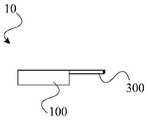
图1所示为光耦合装置10,其中,光波导元件300通过顶侧耦合方案耦合到光波电路100。附接到光波电路100的波导元件300的至少一个末段垂直于或基本上垂直于光波导元件300所附接到的光波电路100的表面区域延伸。Figure 1 shows an
图2所示为光波导元件10的侧耦合方案,其中,波导元件300耦合到光波电路100的一侧。波导元件300从光波电路100横向延伸,因此能够提高光学组件的封装密度,如上所述。FIG. 2 shows a side-coupling scheme of the
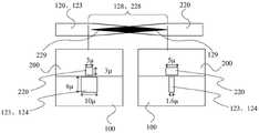
图3所示为一种包括光波电路100、耦合元件200和光波导元件300的光耦合装置10,其中,光波导元件300包括芯层320和包层310。FIG. 3 shows an
耦合元件200可以是具有横向表面区域210、底表面区域230和光路的玻璃块,其中,该光路从横向表面区域210延伸到底表面区域230。第一接合区202设置在横向表面区域210处,并且光波导元件300在第一接合区202处与光路220光耦合。在第一接合区202与底表面区域230之间设置垂直偏移204,使得光波导元件300与光波电路100的第一表面区域110间隔开。The
沿着光波电路100的第一表面区域110,设有光波导120,其中,光波导120包括芯层122、上包层123和下包层124,包层123、124包围或包裹芯层122。Along the
第一凹槽130设置在第一表面区域110中,并且第一凹槽130填充有第一填充材料135。调整上下包层以及第一填充材料的RI,使得在耦合区域20中实现从芯层122到光路220的光耦合。特别地,该布置能够实现光波导120的末段128与光路220的末段228之间的光耦合。末段128和228可以沿着第一表面区域110重叠,即在图3中从左到右重叠,例如,如图4所示,或者可以不重叠,如图3所示。The
在本实施例中,可以在晶圆制造期间在高或中等折射率对比波导120上实现绝热锥形。当光传输到由下包层和外包层氧化物123、124形成的二氧化硅波导时,这种锥形能够在同时处理TM和TE极化时实现低损耗宽带操作。In this embodiment, adiabatic tapers can be implemented on high or medium
将衬底从波导120(波导120可以是,例如,二氧化硅波导,并且衬底可以是硅衬底)下面移除,并且用低折射率材料,即第一填充材料135(例如聚合物),回填衬底。在玻璃块220与二氧化硅波导100之间需要相同或相似的低折射率材料。如图3所示,光波导120不是沿着耦合元件200的整个底表面区域延伸。第一填充材料至少部分地接触耦合元件200的底表面。The substrate is removed from under the waveguide 120 (the
可选地,可以添加另一个薄中等折射率对比波导,以促进到玻璃块的绝热转换(取决于玻璃块以及写入其中的波导的折射率)。这种另一个薄中等折射率对比波导可以位于上包层123的顶部并且紧接在耦合元件200的下方,特别地布置在耦合区域20中。Optionally, another thin medium index contrast waveguide can be added to facilitate adiabatic conversion to the glass block (depending on the refractive index of the glass block and the waveguide written into it). Such another thin medium index contrast waveguide may be located on top of the
这种可选的薄波导层可以添加在氧化物上包层的上方。一个示例可以是70至100nm的SiN层。在这种情况下,光通过上下包层从芯层波导向由二氧化硅形成的波导转换,然后转换到薄波导层。最后,光从该薄波导层转换到玻璃块。This optional thin waveguide layer can be added over the oxide upper cladding. An example could be a 70 to 100 nm SiN layer. In this case, light is converted from the core waveguide to the waveguide formed of silicon dioxide through the upper and lower cladding layers, and then to the thin waveguide layer. Finally, the light is converted from the thin waveguide layer to the glass block.
在玻璃波导220的另一侧,光纤300可以在第一接合区202处轻松粘合或焊接到玻璃块200。由于玻璃波导MFD非常接近光纤MFD,因此损耗可以极低。On the other side of the
图4所示为已经参照图3讨论的光耦合装置10的实施例。FIG. 4 shows an embodiment of the
第二凹槽125可以在光波电路100的第一表面区域110上或顶部的光波导120的上包层123中形成。第二凹槽125可以特别地设置在耦合区域20中。The
在本实施例中,上包层123大部分在高或中等折射率波导120上方被移除。上包层123在足够大的区域上被移除,以使将玻璃块220的放置位置接近薄中等折射率对比波导,即接近光波导120的芯层122。本实施方式可避免硅衬底移除和聚合物的使用,如通过图3中的第一凹槽和第一填充材料所示。In this embodiment, the
图5所示为光耦合装置10,其中,在耦合元件200下方部分地移除上包层123,使得形成第二凹槽(如图4中已经示出的),并且第二凹槽填充有第二填充材料126。Fig. 5 shows the
第二填充材料126的折射率高于上包层123和下包层124的折射率。因此,光信号从光波导120到耦合元件中的光路220的路径的折射率平滑地变化,因此能够在耦合区域20中实现高耦合效率。The refractive index of the
图6所示为光耦合装置10,其中,倏逝波耦合被PIC波导120与玻璃块200之间的对接耦合方法所代替。玻璃块200再次用作模式转换器。玻璃块200的被动对准可能具有低损耗,因为垂直对准可以使用已知参考。在本示例中,使用硅衬底与氧化物包层的交界面。FIG. 6 shows the
SMF 300可以轻松与写入在玻璃块200中的波导220对准。在将波导写入玻璃块的同时,以及使用同一机器的情况下,可以在玻璃块(例如,V形槽)中限定机械特征。这可以通过使用飞秒激光器在玻璃块中诱发“损坏”来实现,这将会非常明显地增加合适化学物质中的蚀刻速率。在激光器写入过程完成之后,可以对晶圆进行化学处理以产生机械对准特征。The
上述过程可以在晶圆级执行,以确保低成本。在形成波导和机械特征之后,可以将晶圆切割成单独的玻璃块。The above process can be performed at the wafer level to ensure low cost. After the waveguides and mechanical features are formed, the wafer can be diced into individual glass blocks.
最好是在芯片仍处于晶圆形式时将玻璃块对准并附接到平面光波电路芯片。在这种情况下,在切割硅光子晶圆并将芯片附接到板或附接在封装中之后,可以使用机械特征将光纤轻松对准并粘合在玻璃上的正确位置。或者,可在将芯片附接到板或封装之后,将光纤附接到玻璃块,并将玻璃块对准。这些选项可以描述为以下步骤。The glass block is preferably aligned and attached to the planar lightwave circuit chip while the chip is still in wafer form. In this case, after dicing the silicon photonics wafer and attaching the chip to a board or in a package, the optical fiber can be easily aligned and glued in the correct position on the glass using mechanical features. Alternatively, after attaching the chip to the board or package, the optical fiber can be attached to the glass block and the glass blocks aligned. These options can be described as the following steps.
定义机械特征;写入波导;抛光以垂直锥化波导;将玻璃块切割成单片;在该步骤之后,完成玻璃块切片并且可以选择以下两个选项:Define the mechanical features; write the waveguide; polish to taper the waveguide vertically; cut the glass block into single pieces; after this step, the glass block slicing is done and two options are available:
在选项1中,在该步骤之后,将具有二氧化硅波导锥形的光子晶圆对准(无源)并键合到玻璃块,切割成单片管芯;将管芯安装到载体/PCB/封装中,引线接合;并对准(有源)和键合SMF光纤。In option 1, after this step, photonic wafer with silicon dioxide waveguide taper is aligned (passive) and bonded to glass block, diced into monolithic die; die mounted to carrier/PCB / package, wire bonding; and aligning (active) and bonding SMF fibers.
在选项2中,先将光纤附接到玻璃块,然后将具有二氧化硅波导锥形的光子晶圆切割成单片管芯;将管芯安装到载体/PCB/封装中/上,引线接合;以及将块与光纤对准(有源)和键合。In option 2, the fiber is attached to the glass block first, then the photonic wafer with the silica waveguide taper is cut into a single die; the die is mounted into/on the carrier/PCB/package, wirebonded ; and aligning (active) and bonding the block to the fiber.
图7A和7B示意性地示出了具有布置在耦合元件200内的光路220的耦合元件200的制备。末段221以角度225相对于耦合元件200的底表面230倾斜。为了在底表面230处提供有效的光信号传输,从底表面230去除材料,直到光路的末段221在底表面230处形成锥形光耦合表面227。FIGS. 7A and 7B schematically illustrate the preparation of a
为了将光从玻璃块绝热耦合到PLC上的波导,玻璃块中的波导可能需要渐缩为点。FLDW技术可以不写入如硅光子学一样的窄尖。该技术的细化是引入垂直锥形以及横向锥形。如果存在垂直锥形,则可以增加沿着锥形的有效折射率变化。提出以与表面成小角度写入波导,然后进行抛光,即从底表面230去除材料。这可以在晶圆级执行。In order to adiabatically couple light from the glass block to the waveguides on the PLC, the waveguides in the glass block may need to taper to points. FLDW technology can avoid writing narrow tips like silicon photonics. A refinement of this technique is the introduction of vertical tapers as well as lateral tapers. If there is a vertical taper, the effective refractive index change along the taper can be increased. It is proposed to write the waveguide at a small angle to the surface and then to polish, ie to remove material from the
图8示意性地示出了图4所示的耦合区域的俯视图。光波导120和上包层123从左向右延伸,并且光波导120的末段128在相同方向上向端129渐缩。光路220从右向左延伸,并且末段228从右向左向端229渐缩。末段128和228在重叠区域中重叠。重叠区域(末段128、228)的长度可以约为2mm。FIG. 8 schematically shows a top view of the coupling region shown in FIG. 4 . The
在重叠波导120和光路220的俯视图下方,示出了两个横截面图,分别指示在重叠区域中的不同位置处的波导120和光路220的轮廓。波导120与光路之间的间隙可以约为1μm。Below the top view of the overlapping
在左下角,示出了玻璃块200内的光路220的末段具有3μm×3μm的横截面,并且示出了在波导120的上包层123和下包层124的横截面的正下方具有6μm×10μm的横截面。这表示在光路220的端229处的横截面。In the lower left corner, the end section of the
在右下角,示出了在波导120的端129处的相反情况。在该端129处,波导120的横截面约为1.6μm×6μm,并且光路220的横截面为5μm×3μm。In the lower right corner, the opposite is shown at the
鉴于波导120和光路220的锥形方向相反,从波导120到光路220的光信号传输效率会增加,反之亦然。Given that the taper directions of the
参考标号列表List of reference signs
10 光耦合装置(optical coupling arrangement)10 Optical coupling arrangement
20 耦合区域(coupling region)20 Coupling region
100 光波电路(lightwave circuit)100 lightwave circuit
110 第一表面区域(first surface area)110 first surface area
120 光波导(optical waveguide)120 Optical waveguide
122 芯层(core)122 core layer (core)
123 上包层(upper cladding)123 Upper cladding
124 下包层(lower cladding)124 Lower cladding
125 第二凹槽(second recess)125 second recess
126 第二填充材料(second filler material)126 Second filler material
128 光波导的末段(end section of the optical waveguide)128 End section of the optical waveguide
129 上下包层的端(end of upper and lower cladding)129 end of upper and lower cladding
130 第一凹槽(first recess)130 first recess
135 第一填充材料(first filler material)135 First filler material
200 耦合元件(coupling element)200 coupling element (coupling element)
202 第一接合区(first junction zone)202 first junction zone
204 垂直偏移(perpendicular offset)204 Perpendicular offset
210 横向表面区域(lateral surface area)210 Lateral surface area
220 光路径(optical path)220 Optical path
221 末段(end section)221 end section
225 倾斜角(inclination angle)225 Inclination angle
227 光耦合表面(optical coupling surface)227 Optical coupling surface
228 光路的末段(end section of optical path)228 End section of optical path
229 光路的端(end of optical path)229 end of optical path
230 底表面区域(bottom surface area)230 bottom surface area
240 第二横向表面区域(second surface area)240 second lateral surface area
300 光波导元件(optical waveguide element)300 Optical waveguide element
310 包层(cladding)310 cladding
320 芯层(core)320 core layer (core)
Claims (13)
Translated fromChineseApplications Claiming Priority (3)
| Application Number | Priority Date | Filing Date | Title |
|---|---|---|---|
| EP15166358.0 | 2015-05-05 | ||
| EP15166358.0AEP3091380B1 (en) | 2015-05-05 | 2015-05-05 | Optical coupling arrangement |
| PCT/CN2015/095117WO2016176982A1 (en) | 2015-05-05 | 2015-11-20 | Optical coupling arrangement |
Publications (2)
| Publication Number | Publication Date |
|---|---|
| CN107003478A CN107003478A (en) | 2017-08-01 |
| CN107003478Btrue CN107003478B (en) | 2020-09-25 |
Family
ID=53040433
Family Applications (1)
| Application Number | Title | Priority Date | Filing Date |
|---|---|---|---|
| CN201580065460.5AActiveCN107003478B (en) | 2015-05-05 | 2015-11-20 | Optical coupling device |
Country Status (4)
| Country | Link |
|---|---|
| US (1) | US10215919B2 (en) |
| EP (1) | EP3091380B1 (en) |
| CN (1) | CN107003478B (en) |
| WO (1) | WO2016176982A1 (en) |
Cited By (1)
| Publication number | Priority date | Publication date | Assignee | Title |
|---|---|---|---|---|
| US11467343B2 (en) | 2019-12-23 | 2022-10-11 | Globalfoundries U.S. Inc. | Optical fiber coupler having hybrid tapered waveguide segments and metamaterial segments |
Families Citing this family (32)
| Publication number | Priority date | Publication date | Assignee | Title |
|---|---|---|---|---|
| US9703038B1 (en) | 2014-07-11 | 2017-07-11 | Acacia Communications, Inc. | Facet optical coupler |
| DE112016000309T5 (en)* | 2015-01-08 | 2017-09-28 | Acacia Communications, Inc. | Horizontal coupling to silicon waveguides |
| WO2018022319A1 (en)* | 2016-07-29 | 2018-02-01 | Corning Optical Communications LLC | Waveguide connector elements and optical assemblies incorporating the same |
| US10571633B1 (en) | 2016-12-23 | 2020-02-25 | Acacia Communications, Inc. | Suspended cantilever waveguide |
| US10416381B1 (en) | 2016-12-23 | 2019-09-17 | Acacia Communications, Inc. | Spot-size-converter design for facet optical coupling |
| US10746935B2 (en)* | 2017-01-30 | 2020-08-18 | The Trustees Of Columbia University In The City Of New York | Fiber-to-waveguide coupling with high alignment tolerance |
| IT201700047081A1 (en)* | 2017-05-02 | 2018-11-02 | St Microelectronics Srl | OPTICAL WAVE GUIDE, MATCHING EQUIPMENT AND CORRESPONDENT PROCEDURE |
| CN109283618A (en)* | 2017-07-21 | 2019-01-29 | 中兴通讯股份有限公司 | A kind of optical wave wire circuit manufacturing method and lightwave circuit, photoelectricity printed circuit board |
| CN107346049A (en)* | 2017-08-08 | 2017-11-14 | 苏州易缆微光电技术有限公司 | A kind of Optical Waveguide Modes spot-size converter and preparation method thereof |
| EP3749996A4 (en)* | 2018-02-05 | 2021-11-24 | Samtec Inc. | Optical interposer |
| GB201803170D0 (en)* | 2018-02-27 | 2018-04-11 | Optoscribe Ltd | Optical apparatus and methods of manufacture thereof |
| US10809456B2 (en)* | 2018-04-04 | 2020-10-20 | Ii-Vi Delaware Inc. | Adiabatically coupled photonic systems with fan-out interposer |
| TWI672480B (en)* | 2018-12-03 | 2019-09-21 | 財團法人工業技術研究院 | Optical measurement apparatus and method |
| CN111352192B (en)* | 2018-12-20 | 2021-08-10 | 青岛海信宽带多媒体技术有限公司 | Optical module |
| WO2020132968A1 (en)* | 2018-12-26 | 2020-07-02 | Huawei Technologies Co., Ltd. | Method and system for testing photonic integration circuit |
| US10989885B2 (en)* | 2019-05-15 | 2021-04-27 | Advanced Semiconductor Engineering, Inc. | Semiconductor package structure and method for manufacturing the same |
| CN112098768B (en)* | 2019-05-30 | 2022-04-29 | 上海新微技术研发中心有限公司 | Method and equipment for testing silicon optical chip |
| US12038608B2 (en)* | 2020-11-09 | 2024-07-16 | Massachusetts Institute Of Technology | Self-aligning photonic interconnections for photonic integrated circuits |
| US11543592B2 (en)* | 2020-11-13 | 2023-01-03 | Ii-Vi Delaware, Inc. | Modular assembly for opto-electronic systems |
| JP2022099500A (en)* | 2020-12-23 | 2022-07-05 | 住友大阪セメント株式会社 | Optical waveguide element and optical modulation device using the same, and optical transmission device |
| US11693169B2 (en)* | 2021-03-08 | 2023-07-04 | Mellanox Technologies, Ltd. | Silicon photonics collimator for wafer level assembly |
| CN113406745A (en)* | 2021-08-19 | 2021-09-17 | 江苏铌奥光电科技有限公司 | Waveguide-to-optical fiber three-dimensional polymer horizontal lens coupler |
| JP7725960B2 (en)* | 2021-09-13 | 2025-08-20 | 古河ファイテルオプティカルコンポーネンツ株式会社 | Optical integrated device, optical integrated circuit wafer, and method for manufacturing optical integrated device |
| CN114137657B (en)* | 2021-12-14 | 2023-08-04 | 武汉光谷信息光电子创新中心有限公司 | Optical coupling structure and silicon-based chip comprising same |
| US20250172760A1 (en)* | 2022-02-28 | 2025-05-29 | Advanced Micro Foundry Pte. Ltd. | Fiber array with side polishing for improved fiber position with wafer substrate or chip |
| WO2023217051A1 (en)* | 2022-05-07 | 2023-11-16 | 上海图灵智算量子科技有限公司 | Waveguide and optical assembly comprising same |
| CN114994833A (en)* | 2022-05-07 | 2022-09-02 | 上海图灵智算量子科技有限公司 | Waveguide and laser comprising same |
| CN114966979B (en)* | 2022-05-07 | 2023-07-18 | 上海图灵智算量子科技有限公司 | Optical component and photoelectric heterogeneous integration method |
| CN115047563B (en)* | 2022-05-22 | 2023-03-17 | 上海图灵智算量子科技有限公司 | Waveguide integrated optical assembly |
| CN115185040B (en)* | 2022-09-09 | 2022-12-13 | 之江实验室 | Passive alignment optical packaging structure of silicon photonic chip and optical switch equipment |
| WO2024252770A1 (en)* | 2023-06-05 | 2024-12-12 | パナソニックIpマネジメント株式会社 | Optical transmission path and method for manufacturing same |
| GB202316378D0 (en) | 2023-10-26 | 2023-12-13 | Univ College Cork National Univ Of Ireland | Photonic integrated circuit micro-optical coupler for cryogenic environments |
Citations (5)
| Publication number | Priority date | Publication date | Assignee | Title |
|---|---|---|---|---|
| US20050123244A1 (en)* | 2003-12-03 | 2005-06-09 | Block Bruce A. | Embedded optical waveguide coupler |
| CN1685256A (en)* | 2001-10-30 | 2005-10-19 | 斯邦恩特光子学公司 | Optical bonding apparatus and method using optical power lateral transfer |
| US7539373B1 (en)* | 2007-11-26 | 2009-05-26 | Onechip Photonics Inc. | Integrated lateral mode converter |
| CN102565955A (en)* | 2012-01-16 | 2012-07-11 | 中国科学院半导体研究所 | Electric tunable grating coupler |
| US8483528B2 (en)* | 2008-02-29 | 2013-07-09 | Google Inc. | Optical mode transformer, in particular for coupling an optical fiber and a high-index contrast waveguide |
Family Cites Families (8)
| Publication number | Priority date | Publication date | Assignee | Title |
|---|---|---|---|---|
| US6937335B2 (en)* | 2002-03-08 | 2005-08-30 | Paul Victor Mukai | Dynamic alignment of optical fibers to optical circuit devices such as planar lightwave circuits |
| US6934427B2 (en)* | 2002-03-12 | 2005-08-23 | Enablence Holdings Llc | High density integrated optical chip with low index difference waveguide functions |
| WO2004068542A2 (en) | 2003-01-24 | 2004-08-12 | Xponent Photonics Inc | Etched-facet semiconductor optical component with integrated end-coupled waveguide and methods of fabrication and use thereof |
| US7289697B2 (en)* | 2005-09-27 | 2007-10-30 | Lucent Technologies Inc. | Optical pulse shaper having hybrid planar lightwave circuit and free-space optics with MEMS piston-motion micromirrors and feedback control |
| DE102006039601A1 (en)* | 2006-08-24 | 2008-04-30 | Erni Electronics Gmbh | Optical coupling element |
| EP2676321B1 (en) | 2011-07-04 | 2018-09-05 | Huawei Technologies Co., Ltd. | Coupling arrangement |
| US8724937B2 (en)* | 2011-12-20 | 2014-05-13 | International Business Machines Corporation | Fiber to wafer interface |
| US9136672B2 (en)* | 2012-11-29 | 2015-09-15 | Agency For Science, Technology And Research | Optical light source |
- 2015
- 2015-05-05EPEP15166358.0Apatent/EP3091380B1/enactiveActive
- 2015-11-20WOPCT/CN2015/095117patent/WO2016176982A1/ennot_activeCeased
- 2015-11-20CNCN201580065460.5Apatent/CN107003478B/enactiveActive
- 2017
- 2017-08-17USUS15/679,875patent/US10215919B2/enactiveActive
Patent Citations (5)
| Publication number | Priority date | Publication date | Assignee | Title |
|---|---|---|---|---|
| CN1685256A (en)* | 2001-10-30 | 2005-10-19 | 斯邦恩特光子学公司 | Optical bonding apparatus and method using optical power lateral transfer |
| US20050123244A1 (en)* | 2003-12-03 | 2005-06-09 | Block Bruce A. | Embedded optical waveguide coupler |
| US7539373B1 (en)* | 2007-11-26 | 2009-05-26 | Onechip Photonics Inc. | Integrated lateral mode converter |
| US8483528B2 (en)* | 2008-02-29 | 2013-07-09 | Google Inc. | Optical mode transformer, in particular for coupling an optical fiber and a high-index contrast waveguide |
| CN102565955A (en)* | 2012-01-16 | 2012-07-11 | 中国科学院半导体研究所 | Electric tunable grating coupler |
Cited By (1)
| Publication number | Priority date | Publication date | Assignee | Title |
|---|---|---|---|---|
| US11467343B2 (en) | 2019-12-23 | 2022-10-11 | Globalfoundries U.S. Inc. | Optical fiber coupler having hybrid tapered waveguide segments and metamaterial segments |
Also Published As
| Publication number | Publication date |
|---|---|
| CN107003478A (en) | 2017-08-01 |
| EP3091380A1 (en) | 2016-11-09 |
| EP3091380B1 (en) | 2021-07-07 |
| US20170343734A1 (en) | 2017-11-30 |
| US10215919B2 (en) | 2019-02-26 |
| WO2016176982A1 (en) | 2016-11-10 |
Similar Documents
| Publication | Publication Date | Title |
|---|---|---|
| CN107003478B (en) | Optical coupling device | |
| KR101866495B1 (en) | Two-stage Adiabatically Coupled Photonic Systems | |
| CN107407778B (en) | Optically coupled waveguide | |
| US10288805B2 (en) | Coupling between optical devices | |
| US10564374B2 (en) | Electro-optical interconnect platform | |
| US8319237B2 (en) | Integrated optical receiver architecture for high speed optical I/O applications | |
| JP6172679B2 (en) | Optical coupling structure, semiconductor device, optical interconnect structure for multi-chip module, and manufacturing method for optical coupling structure | |
| KR101591847B1 (en) | Efficient silicon-on-insulator grating coupler | |
| US20190265415A1 (en) | Optical apparatus and methods of manufacture thereof | |
| KR102313684B1 (en) | Optical coupler | |
| CN113474705A (en) | Edge coupling through unetched surfaces of photonic chips | |
| CN106125195A (en) | Optical coupling mechanism | |
| US11067754B2 (en) | Simultaneous electrical and optical connections for flip chip assembly | |
| EP2932320A1 (en) | Fiber optic coupler array | |
| US10422967B2 (en) | Optical coupling apparatus and method | |
| CN109791251B (en) | Light beam spot size converter | |
| Brusberg et al. | Single-mode glass waveguide platform for DWDM chip-to-chip interconnects | |
| KR20140146661A (en) | Method and apparatus providing a waveguide and an evanescent field coupled photonic detector | |
| KR20120118264A (en) | Optical connecter and optical apparatus having the same | |
| CN114966975A (en) | A Probe Fiber for Silicon Optical Wafer End-Face Coupling Test | |
| CN115047562B (en) | Silicon photon collimator for wafer level assembly | |
| Tekin et al. | Fibre-array optical interconnection for silicon photonics | |
| CN117148493A (en) | Optical chip and method for manufacturing the same | |
| CN118151314A (en) | Package and method of forming the same |
Legal Events
| Date | Code | Title | Description |
|---|---|---|---|
| PB01 | Publication | ||
| PB01 | Publication | ||
| SE01 | Entry into force of request for substantive examination | ||
| SE01 | Entry into force of request for substantive examination | ||
| GR01 | Patent grant | ||
| GR01 | Patent grant |