CN106980403B - Touch control display panel - Google Patents
Touch control display panelDownload PDFInfo
- Publication number
- CN106980403B CN106980403BCN201610033380.8ACN201610033380ACN106980403BCN 106980403 BCN106980403 BCN 106980403BCN 201610033380 ACN201610033380 ACN 201610033380ACN 106980403 BCN106980403 BCN 106980403B
- Authority
- CN
- China
- Prior art keywords
- sensing
- pixel
- voltage
- type transistor
- unit
- Prior art date
- Legal status (The legal status is an assumption and is not a legal conclusion. Google has not performed a legal analysis and makes no representation as to the accuracy of the status listed.)
- Active
Links
Images


Classifications
- G—PHYSICS
- G06—COMPUTING OR CALCULATING; COUNTING
- G06F—ELECTRIC DIGITAL DATA PROCESSING
- G06F3/00—Input arrangements for transferring data to be processed into a form capable of being handled by the computer; Output arrangements for transferring data from processing unit to output unit, e.g. interface arrangements
- G06F3/01—Input arrangements or combined input and output arrangements for interaction between user and computer
- G06F3/03—Arrangements for converting the position or the displacement of a member into a coded form
- G06F3/041—Digitisers, e.g. for touch screens or touch pads, characterised by the transducing means
- G06F3/042—Digitisers, e.g. for touch screens or touch pads, characterised by the transducing means by opto-electronic means
- G—PHYSICS
- G06—COMPUTING OR CALCULATING; COUNTING
- G06F—ELECTRIC DIGITAL DATA PROCESSING
- G06F3/00—Input arrangements for transferring data to be processed into a form capable of being handled by the computer; Output arrangements for transferring data from processing unit to output unit, e.g. interface arrangements
- G06F3/01—Input arrangements or combined input and output arrangements for interaction between user and computer
- G06F3/03—Arrangements for converting the position or the displacement of a member into a coded form
- G06F3/041—Digitisers, e.g. for touch screens or touch pads, characterised by the transducing means
- G06F3/0412—Digitisers structurally integrated in a display
- G—PHYSICS
- G06—COMPUTING OR CALCULATING; COUNTING
- G06F—ELECTRIC DIGITAL DATA PROCESSING
- G06F3/00—Input arrangements for transferring data to be processed into a form capable of being handled by the computer; Output arrangements for transferring data from processing unit to output unit, e.g. interface arrangements
- G06F3/01—Input arrangements or combined input and output arrangements for interaction between user and computer
- G06F3/03—Arrangements for converting the position or the displacement of a member into a coded form
- G06F3/041—Digitisers, e.g. for touch screens or touch pads, characterised by the transducing means
- G06F3/0416—Control or interface arrangements specially adapted for digitisers
- G06F3/04166—Details of scanning methods, e.g. sampling time, grouping of sub areas or time sharing with display driving
Landscapes
- Engineering & Computer Science (AREA)
- General Engineering & Computer Science (AREA)
- Theoretical Computer Science (AREA)
- Human Computer Interaction (AREA)
- Physics & Mathematics (AREA)
- General Physics & Mathematics (AREA)
- Liquid Crystal (AREA)
- Control Of Indicators Other Than Cathode Ray Tubes (AREA)
- Liquid Crystal Display Device Control (AREA)
- Position Input By Displaying (AREA)
Abstract
Translated fromChinese
Description
Translated fromChinese技术领域technical field
本发明涉及一种显示设备,尤其涉及一种触控显示面板。The present invention relates to a display device, in particular to a touch display panel.
背景技术Background technique
一般而言,触控显示面板包括多个显示单元与多个触控单元,其中多个显示单元可以构成显示区域,多个触控单元可内建于触控显示面板中。目前,触控单元依照其感测方式的不同而大致上区分为电阻式触控单元、电容式触控单元、光学式触控单元、声波式触控单元以及电磁式触控单元。当使用者以手指或是触控笔等接触触控显示面板时,在被接触的位置上的触控单元会产生电性上的改变,诸如电容改变、电流改变、电阻改变等。此等电性上的改变会转换为电子信号并经运算处理而输出适当的指令以操作电子装置。Generally speaking, a touch display panel includes a plurality of display units and a plurality of touch units, wherein the plurality of display units may constitute a display area, and the plurality of touch units may be built in the touch display panel. Currently, touch units are roughly classified into resistive touch units, capacitive touch units, optical touch units, acoustic wave touch units, and electromagnetic touch units according to different sensing methods. When a user touches the touch display panel with a finger or a stylus, the touch unit at the touched position will change electrical properties, such as capacitance change, current change, resistance change, and the like. These electrical changes will be converted into electrical signals and processed by operations to output appropriate commands to operate the electronic device.
触控显示面板具有显示区以及周边区,其中显示区除了设置用以显示画面的像素数组外,亦设置触控感测数组以感测触控事件的发生,其中用以驱动像素数组的扫描线与数据传输线以及用以驱动触控感测数组的扫描线以及感测信号传输线为分别设置,因而使触控显示面板无法具有较佳的开口率。此外,为了设置数量众多的信号传输线,触控显示面板的周边区将占据一定的面积。如此一来,将很难满足触控显示面板的窄边框设计需求。The touch display panel has a display area and a peripheral area. In the display area, in addition to a pixel array for displaying a picture, a touch sensing array is also arranged to sense the occurrence of a touch event, and the scan lines used to drive the pixel array are arranged in the display area. The data transmission lines, the scan lines for driving the touch sensing arrays, and the sensing signal transmission lines are arranged separately, so that the touch display panel cannot have a better aperture ratio. In addition, in order to set up a large number of signal transmission lines, the peripheral area of the touch display panel will occupy a certain area. As a result, it will be difficult to meet the narrow border design requirements of the touch display panel.
发明内容SUMMARY OF THE INVENTION
本发明提供一种触控显示面板,可有效地大幅提高触控显示面板的开口率并满足触控显示面板的窄边框设计需求。The present invention provides a touch display panel, which can effectively greatly improve the aperture ratio of the touch display panel and meet the design requirements of the touch display panel for narrow borders.
本发明的触控显示面板,包括扫描线、第一信号传输线、像素单元以及触控感测单元。其中像素单元耦接扫描线与第一信号传输线。触控感测单元耦接扫描线以及像素单元,触控感测单元包括开关单元以及感测像素单元。开关单元的控制端耦接扫描线与像素单元。感测像素单元耦接扫描线与开关单元,感测触控操作而对应产生触控感测信号,其中扫描线于其扫描期间进入显示模式与触控模式,扫描线于显示模式中接收第一电压,以断开开关单元并致能像素单元自第一信号传输线接收像素电压信号,扫描线并于触控模式中接收第二电压,以导通开关单元并禁能像素单元接收像素电压信号,而使感测像素单元通过开关单元输出触控感测信号至第一信号传输线,其中第一电压大于第二电压。The touch display panel of the present invention includes a scan line, a first signal transmission line, a pixel unit and a touch sensing unit. The pixel unit is coupled to the scan line and the first signal transmission line. The touch sensing unit is coupled to the scan line and the pixel unit, and the touch sensing unit includes a switch unit and a sensing pixel unit. The control end of the switch unit is coupled to the scan line and the pixel unit. The sensing pixel unit is coupled to the scan line and the switch unit, and senses the touch operation to generate a touch sensing signal correspondingly, wherein the scan line enters the display mode and the touch mode during its scanning period, and the scan line receives the first touch in the display mode. voltage to turn off the switch unit and enable the pixel unit to receive the pixel voltage signal from the first signal transmission line, the scan line to receive the second voltage in the touch mode to turn on the switch unit and disable the pixel unit to receive the pixel voltage signal, The sensing pixel unit outputs a touch sensing signal to the first signal transmission line through the switch unit, wherein the first voltage is greater than the second voltage.
在本发明的一实施例中,上述的开关单元包括P型晶体管,P型晶体管的栅极耦接扫描线,P型晶体管的源极耦接感测像素单元,P型晶体管的漏极耦接第一信号传输线。In an embodiment of the present invention, the above-mentioned switch unit includes a P-type transistor, the gate of the P-type transistor is coupled to the scan line, the source of the P-type transistor is coupled to the sensing pixel unit, and the drain of the P-type transistor is coupled to the first signal transmission line.
在本发明的一实施例中,上述的感测像素单元包括重置单元以及感测单元。重置单元耦接扫描线。感测单元耦接重置单元与开关单元,感测触控操作而对应产生触控感测信号,重置单元于扫描线接收第一电压时重置感测单元。In an embodiment of the present invention, the above-mentioned sensing pixel unit includes a reset unit and a sensing unit. The reset unit is coupled to the scan line. The sensing unit is coupled to the reset unit and the switch unit, and senses the touch operation to generate a touch sensing signal correspondingly. The reset unit resets the sensing unit when the scan line receives the first voltage.
在本发明的一实施例中,上述的重置单元包括第一感测N型晶体管,其栅极耦接扫描线,第一感测N型晶体管的漏极耦接重置电压,第一感测N型晶体管的源极耦接感测单元,第一感测N型晶体管于扫描线接收第一电压时被导通而输出重置电压重置感测单元。In an embodiment of the present invention, the above-mentioned reset unit includes a first sensing N-type transistor, the gate of which is coupled to the scan line, the drain of the first sensing N-type transistor is coupled to the reset voltage, and the first sensing N-type transistor is coupled to the reset voltage. The source of the sensing N-type transistor is coupled to the sensing unit, and the first sensing N-type transistor is turned on when the scan line receives the first voltage to output a reset voltage to reset the sensing unit.
在本发明的一实施例中,上述的感测单元包括感测电容、光二极管以及第二感测N型晶体管。光二极管与感测电容并联于第一感测N型晶体管的源极与共同电压之间。第二感测N型晶体管的栅极耦接第一感测N型晶体管的源极,第二感测N型晶体管的漏极耦接开关单元,第二感测N型晶体管的源极耦接参考电压。In an embodiment of the present invention, the above-mentioned sensing unit includes a sensing capacitor, a photodiode, and a second sensing N-type transistor. The photodiode and the sensing capacitor are connected in parallel between the source of the first sensing N-type transistor and the common voltage. The gate of the second sensing N-type transistor is coupled to the source of the first sensing N-type transistor, the drain of the second sensing N-type transistor is coupled to the switch unit, and the source of the second sensing N-type transistor is coupled to reference voltage.
在本发明的一实施例中,上述的扫描线在显示模式中更于接收第一电压后接收第三电压,并在触控模式中于接收第二电压后接收第三电压,第三电压用以关闭第一感测N型晶体管、断开开关单元并禁能像素单元接收像素电压信号。In an embodiment of the present invention, the above-mentioned scan line receives a third voltage after receiving the first voltage in the display mode, and receives a third voltage after receiving the second voltage in the touch mode. The first sensing N-type transistor is turned off, the switch unit is turned off, and the pixel unit is disabled to receive the pixel voltage signal.
在本发明的一实施例中,上述的像素单元包括第一子像素单元,第一子像素单元包括第一像素N型晶体管、第一液晶电容以及第一储存电容。第一像素N型晶体管的栅极耦接扫描线,第一像素N型晶体管的漏极耦接第一信号传输线。第一储存电容与第一液晶电容并联于第一像素N型晶体管的源极与共同电压之间。In an embodiment of the present invention, the above-mentioned pixel unit includes a first sub-pixel unit, and the first sub-pixel unit includes a first pixel N-type transistor, a first liquid crystal capacitor, and a first storage capacitor. The gate of the N-type transistor of the first pixel is coupled to the scan line, and the drain of the N-type transistor of the first pixel is coupled to the first signal transmission line. The first storage capacitor and the first liquid crystal capacitor are connected in parallel between the source of the N-type transistor of the first pixel and the common voltage.
在本发明的一实施例中,上述的触控显示面板还包括第二信号传输线以及第三信号传输线,像素单元还包括第二子像素单元以及第三子像素单元。第二子像素单元包括第二像素N型晶体管、第二液晶电容以及第二储存电容。第二像素N型晶体管的栅极耦接扫描线,第二像素N型晶体管的漏极耦接第二信号传输线。第二储存电容与第二液晶电容并联于第二像素N型晶体管的源极与共同电压之间。第三子像素单元包括第三像素N型晶体管、第三液晶电容以及第三储存电容。第三像素N型晶体管的栅极耦接扫描线,第三像素N型晶体管的漏极耦接第三信号传输线。第三储存电容与第三液晶电容并联于第三像素N型晶体管的源极与共同电压之间。In an embodiment of the present invention, the above-mentioned touch display panel further includes a second signal transmission line and a third signal transmission line, and the pixel unit further includes a second sub-pixel unit and a third sub-pixel unit. The second sub-pixel unit includes a second pixel N-type transistor, a second liquid crystal capacitor, and a second storage capacitor. The gate of the N-type transistor of the second pixel is coupled to the scan line, and the drain of the N-type transistor of the second pixel is coupled to the second signal transmission line. The second storage capacitor and the second liquid crystal capacitor are connected in parallel between the source of the N-type transistor of the second pixel and the common voltage. The third sub-pixel unit includes a third pixel N-type transistor, a third liquid crystal capacitor, and a third storage capacitor. The gate of the N-type transistor of the third pixel is coupled to the scan line, and the drain of the N-type transistor of the third pixel is coupled to the third signal transmission line. The third storage capacitor and the third liquid crystal capacitor are connected in parallel between the source of the N-type transistor of the third pixel and the common voltage.
在本发明的一实施例中,上述的感测像素单元、第一子像素单元、第二子像素单元以及第三子像素单元于显示面板上占据相同或不同的面积。In an embodiment of the present invention, the above-mentioned sensing pixel unit, first sub-pixel unit, second sub-pixel unit and third sub-pixel unit occupy the same or different areas on the display panel.
在本发明的一实施例中,上述的第一电压为正电压,第二电压为负电压。In an embodiment of the present invention, the above-mentioned first voltage is a positive voltage, and the second voltage is a negative voltage.
基于上述,本发明实施例的扫描线于其扫描期间进入显示模式与触控模式,其中于显示模式中扫描线接收一第一电压,以断开开关单元并致能像素单元自第一信号传输线接收像素电压信号,于触控模式中扫描线接收第二电压,以导通开关单元并禁能对应的像素单元接收像素电压信号,而使感测像素单元通过开关单元输出触控感测信号至第一信号传输线,其中第一电压大于第二电压。如此藉由共享第一信号传输线来传输像素电压信号以及触控感测信号,可有效地大幅提高触控显示面板的开口率并满足触控显示面板的窄边框设计需求。Based on the above, the scan line of the embodiment of the present invention enters the display mode and the touch mode during the scan period, wherein in the display mode, the scan line receives a first voltage to turn off the switch unit and enable the pixel unit from the first signal transmission line Receive the pixel voltage signal, and in the touch mode, the scan line receives the second voltage to turn on the switch unit and disable the corresponding pixel unit from receiving the pixel voltage signal, so that the sensing pixel unit outputs the touch sensing signal through the switch unit to The first signal transmission line, wherein the first voltage is greater than the second voltage. In this way, by sharing the first signal transmission line to transmit the pixel voltage signal and the touch sensing signal, the aperture ratio of the touch display panel can be effectively improved and the narrow frame design requirements of the touch display panel can be met.
为让本发明的上述特征和优点能更明显易懂,下文特举实施例,并配合附图作详细说明如下。In order to make the above-mentioned features and advantages of the present invention more obvious and easy to understand, the following embodiments are given and described in detail with the accompanying drawings as follows.
附图说明Description of drawings
图1是依照本发明的一实施例的触控显示设备的示意图;FIG. 1 is a schematic diagram of a touch display device according to an embodiment of the present invention;
图2是依照本发明的一实施例的触控显示面板的示意图;FIG. 2 is a schematic diagram of a touch display panel according to an embodiment of the present invention;
图3是依照本发明另一实施例的触控显示面板的示意图;3 is a schematic diagram of a touch display panel according to another embodiment of the present invention;
图4是依照本发明的一实施例的扫描线电压的示意图;4 is a schematic diagram of scan line voltages according to an embodiment of the present invention;
图5~图7是依照本发明实施例的像素单元与感测像素单元的配置示意图。5 to 7 are schematic diagrams illustrating configurations of a pixel unit and a sensing pixel unit according to an embodiment of the present invention.
附图标记:Reference number:
100:触控显示设备100: Touch Display Devices
102:数据驱动器102: Data Drive
104:栅极驱动器104: Gate Drivers
106:触控显示面板106: Touch display panel
108:感测放大器108: Sense Amplifier
202:开关单元202: Switch unit
204:感测像素单元204: Sensing pixel unit
302:重置单元302: Reset unit
304:感测单元304: Sensing unit
SL1:扫描线SL1: scan line
DL1:信号传输线DL1: Signal transmission line
P1:像素单元P1: pixel unit
TC1:触控感测单元TC1: Touch Sensing Unit
Q1:P型晶体管Q1: P-type transistor
M1~M5:N型晶体管M1~M5: N-type transistor
C1:感测电容C1: Sensing Capacitor
PD1:光二极管PD1: Photodiode
Vreset:重置电压Vreset: reset voltage
Vcom:共同电压Vcom: common voltage
Vdd:参考电压Vdd: reference voltage
SP1、SP2、SP3:子像素单元SP1, SP2, SP3: sub-pixel units
CS1、CS2、CS3:储存电容CS1, CS2, CS3: Storage capacitors
CL1、CL2、CL3:液晶电容CL1, CL2, CL3: Liquid crystal capacitors
V1、V2、V3:电压V1, V2, V3: Voltage
具体实施方式Detailed ways
图1是依照本发明的一实施例的触控显示设备的示意图,请参照图1。触控显示设备100包括数据驱动器102、栅极驱动器104、触控显示面板106以及感测放大器108,其中触控显示面板106耦接数据驱动器102、栅极驱动器104以及感测放大器108,触控显示面板106可例如为有机发光二极管(Organic Light Emitting Diode,OLED)显示面板或液晶显示面板,然不以此为限。进一步来说,触控显示面板106可包括多条扫描线SL1、多条信号传输线DL1、多个像素单元P1以及多个触控感测单元TC1,其中多条扫描线SL1以及多条信号传输线DL1交叉地配置于触控显示面板106上,多个像素单元P1以数组的方式排列于触控显示面板106上,并分别耦接对应的扫描线SL1以及信号传输线DL1。另外,多个触控感测单元TC1亦以数组的方式排列于触控显示面板106上,分别耦接对应的扫描线SL1,并与对应的像素单元P1耦接至同一条信号传输线。其中多条扫描线SL1依序地被驱动,以于各扫描线的扫描期间使各扫描线SL1上的像素单元P1自其对应的信号传输线DL1接收来自数据驱动器102的像素电压信号而进行影像画面的显示,并使各扫描线SL1上的触控感测单元TC1将其检测到的触控感测信号通过其对应的信号传输线DL1输出给感测放大器108,以放大触控感测信号并将其输出给后端用以判断触控位置的电路。FIG. 1 is a schematic diagram of a touch display device according to an embodiment of the present invention, please refer to FIG. 1 . The
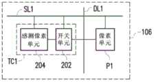
详细来说,触控显示面板106可例如以图2的方式来实施,为便于说明,在图2实施例中仅显示出一个触控感测单元TC1与一个像素单元P1,然实际应用上并不以此为限。在本实施例中触控感测单元TC1可包括开关单元202与感测像素单元204,其中开关单元202耦接扫描线SL1以及信号传输线DL1,感测像素单元204耦接扫描线SL1以及开关单元202。开关单元202的控制端可接收来自扫描线SL1的驱动电压,而改变其导通状态,感测像素单元204则可感测触控操作而对应产生触控感测信号,例如感测手指或触控笔等输入工具的触控操作,并于开关单元202被导通时传输触控感测信号至信号传输线DL1。进一步来说,扫描线SL1于其扫描期间进入显示模式与触控模式,其中扫描线SL1于显示模式中接收第一电压,以断开开关单元202并致能像素单元P1自信号传输线DL1接收像素电压信号。而在触控模式中,扫描线SL1接收第二电压,以导通开关单元204并禁能像素单元P1接收像素电压信号,此时感测像素单元可通过开关单元202输出触控感测信号至信号传输线DL1,以供感测放大器108以及后端的电路进行触控感测信号的处理,与触控位置的判断,其中第一电压大于该第二电压。In detail, the
图3是依照本发明另一实施例的触控显示面板的示意图,请参照图3。详细来说,图2的触控显示面板106可例如以图3的方式来实施。在本实施例中,开关单元202包括P型晶体管Q1,P型晶体管Q1的栅极耦接扫描线SL1,P型晶体管Q1的源极与漏极分别耦接感测像素单元204与信号传输线DL1。另外,感测像素单元204则包括重置单元302以及感测单元304,重置单元耦接扫描线SL1,而感测单元304则耦接重置单元302以及开关单元202。感测单元304可用以感测触控操作,而对应产生触控感测信号至开关单元202,重置单元则可于扫描线SL1接收第一电压时重置感测单元304的感测值,以避免感测单元304于下次进行触控操作的感测时,其所输出的触控感测信号的感测值受到前次感测值的影响,进而造成触控位置的误判。FIG. 3 is a schematic diagram of a touch display panel according to another embodiment of the present invention. Please refer to FIG. 3 . In detail, the
在本实施例中,重置单元302可例如以第一感测N型晶体管M1来实施,而感测单元304则可以第二感测N型晶体管M2、感测电容C1以及光二极管PD1来实施。其中第一感测N型晶体管M1的栅极耦接扫描线SL1,漏极耦接重置电压Vreset,源极则耦接第二感测N型晶体管M2的栅极。感测单元304中的感测电容C1与光二极管并联于第二感测N型晶体管M2的栅极与共同电压Vcom之间,而第二感测N型晶体管M2的源极与漏极分别耦接参考电压Vdd以及开关单元202(P型晶体管Q1的源极)。另一方面,本实施例的像素单元P1可包括子像素单元SP1、SP2以及SP3,其可例如分别用以显示红色、绿色与蓝色,各个子像素单元分别包括一像素N型晶体管(M3、M4、M5)、一储存电容(CS1、CS2、CS3)以及一液晶电容(CL1、CL2、CL3)。在子像素单元SP1中,第一像素N型晶体管M3的栅极耦接扫描线SL1,漏极耦接其对应的信号传输线DL1,源极则耦接储存电容CS1以及液晶电容CL1的一端,而储存电容CS1以及液晶电容CL1的另一端则耦接共同电压Vcom。类似地,子像素单元SP2、子像素单元SP3中晶体管、储存电容以及液晶电容的耦接方式类似于子像素单元SP1,因此在此不再赘述。In this embodiment, the
值得注意的是,像素单元P1所包括的子像素单元的个数并不以图3实施例为限,在其它实施例中,像素单元P1以可包括更多或更少的子像素单元。此外,与触控感测单元TC1共同耦接信号传输线的子像素单元亦可为子像素单元SP2或子像素单元SP3,不以子像素单元SP1为限。It should be noted that the number of sub-pixel units included in the pixel unit P1 is not limited to the embodiment shown in FIG. 3 , and in other embodiments, the pixel unit P1 may include more or less sub-pixel units. In addition, the sub-pixel unit that is commonly coupled to the signal transmission line with the touch sensing unit TC1 can also be the sub-pixel unit SP2 or the sub-pixel unit SP3, which is not limited to the sub-pixel unit SP1.
图4是依照本发明的一实施例的扫描线电压的示意图,请同时参照图3与图4。如图4所示,当扫描线SL1进入扫描期间后先进入显示模式。在显示模式期间,扫描线SL1先接收第一电压V1,其电压值大于0且可导通N型晶体管M1、N型晶体管M3、N型晶体管M4、N型晶体管M5并关闭P型晶体管Q1,此时重置电压Vreset可通过第一感测N型晶体管M1被传送至第二感测N型晶体管M2的栅极,而重置感测电容C1以及光二极管PD1上的跨压。在进行重置的期间,由于P型晶体管Q1处于关闭状态,因此即使第二感测N型晶体管M2被导通,参考电压Vdd亦不会通过P型晶体管Q1被传送至信号传输线DL1,因此不会对信号传输在线的电压产生影响。FIG. 4 is a schematic diagram of scan line voltages according to an embodiment of the present invention. Please refer to FIG. 3 and FIG. 4 at the same time. As shown in FIG. 4 , when the scanning line SL1 enters the scanning period, it first enters the display mode. During the display mode, the scan line SL1 first receives the first voltage V1, which is greater than 0 and can turn on the N-type transistor M1, N-type transistor M3, N-type transistor M4, N-type transistor M5 and turn off the P-type transistor Q1, At this time, the reset voltage Vreset can be transmitted to the gate of the second sensing N-type transistor M2 through the first sensing N-type transistor M1 to reset the cross-voltage on the sensing capacitor C1 and the photodiode PD1 . During the reset period, since the P-type transistor Q1 is in an off state, even if the second sensing N-type transistor M2 is turned on, the reference voltage Vdd will not be transmitted to the signal transmission line DL1 through the P-type transistor Q1, so there is no It will affect the voltage of the signal transmission line.
另一方面,由于像素N型晶体管M3、N型晶体管M4、N型晶体管M5被导通,因此子像素单元SP1、子像素单元SP2以及子像素单元SP3中的储存电容(CS1、CS2、CS3)以及液晶电容(CL1、CL2、CL3)可分别自其对应的信号传输线接收像素电压信号。在接收完像素电压信号后,扫描线SL1接收的电压转为第三电压V3,第三电压V3可使N型晶体管M1、N型晶体管M3、N型晶体管M4、N型晶体管M5以及P型晶体管Q1皆进入关闭的状态。在显示模式中扫描在线的电压转为第三电压V3的期间,像素单元P1中的子像素单元SP1、子像素单元SP2以及子像素单元SP3被禁能而停止接收像素电压信号,并依据接收到的像素电压信号进行影像画面的显示。On the other hand, since the pixel N-type transistor M3, N-type transistor M4, and N-type transistor M5 are turned on, the storage capacitors (CS1, CS2, CS3) in the sub-pixel unit SP1, the sub-pixel unit SP2, and the sub-pixel unit SP3 And the liquid crystal capacitors ( CL1 , CL2 , CL3 ) can respectively receive pixel voltage signals from their corresponding signal transmission lines. After the pixel voltage signal is received, the voltage received by the scan line SL1 is converted into a third voltage V3, and the third voltage V3 can make the N-type transistor M1, N-type transistor M3, N-type transistor M4, N-type transistor M5 and P-type transistor Q1 are all in the off state. During the period when the voltage of the scanning line is changed to the third voltage V3 in the display mode, the sub-pixel unit SP1, the sub-pixel unit SP2 and the sub-pixel unit SP3 in the pixel unit P1 are disabled and stop receiving the pixel voltage signal, and according to the received The pixel voltage signal of the image screen is displayed.
此外,当扫描线SL1进入触控模式后,扫描线SL1先接收第二电压V2,其电压值小于0且可关闭N型晶体管M1、N型晶体管M3、N型晶体管M4、N型晶体管M5并开启P型晶体管Q1。因此,在触控模式中,子像素单元SP1、子像素单元SP2以及子像素单元SP3仍继续执行画面的显示,且其已不需接收像素电压信号,此时,感测像素单元204便可利用闲置的信号传输线DL1来传输触控感测信号。详细来说,当感测像素单元204接收触控操作时,光二极管PD1可接收输入工具反射像素单元P1的光线,并将其转为电信号,进而改变感测电容C1上的跨压,即改变第二感测N型晶体管M2的栅极电压。第二感测N型晶体管M2可依据其栅极电压改变其导通状态,而决定是否将参考电压Vdd输出至信号传输线DL1,如此便可依据信号传输线DL1是否接收到参考电压Vdd来判断对应感测像素单元204的位置是否被触碰。其中在传送完触控感测信号后,扫描线SL1接收的电压再次转为第三电压V3,而使N型晶体管M1、N型晶体管M3、N型晶体管M4、N型晶体管M5以及P型晶体管Q1皆进入关闭的状态,在显示模式中扫描在线的电压转为第三电压V3的期间,可用以进行触控位置的判断。另外,由于感测电容C1上的跨压于显示模式期间已被重置,因此相邻扫描期间感测电容C1上的跨压并不会互相影响,而可确保触控位置判断的正确性。值得注意的是,上述实施例扫描线SL1为先进入显示模式后再进入触控模式,然在部分实施例中,扫描线SL1亦可先进入触控模式再进入显示模式。In addition, after the scan line SL1 enters the touch mode, the scan line SL1 first receives the second voltage V2, the voltage value of which is less than 0, and the N-type transistor M1, N-type transistor M3, N-type transistor M4, and N-type transistor M5 can be turned off and turned off. Turn on the P-type transistor Q1. Therefore, in the touch mode, the sub-pixel unit SP1, the sub-pixel unit SP2, and the sub-pixel unit SP3 still continue to perform screen display, and they no longer need to receive pixel voltage signals. At this time, the
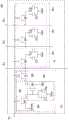
图5~图7是依照本发明实施例的像素单元与感测像素单元204的配置示意图,请参照图5~图7。在图5实施例中,感测像素单元204、子像素单元SP1、子像素单元SP2以及子像素单元SP3在触控显示面板106上的配置方式可例如为并列地配置于触控显示面板106上,其中感测像素单元204、子像素单元SP1、子像素单元SP2以及子像素单元SP3占据相同的面积。其中,感测像素单元204、子像素单元SP1、子像素单元SP2以及子像素单元SP3在触控显示面板106上的配置方式并不以图5实施例为限,如在图6实施例中,感测像素单元204、子像素单元SP1、子像素单元SP2以及子像素单元SP3亦可以以棋盘格的形式配置于触控显示面板106上,其中感测像素单元204、子像素单元SP1、子像素单元SP2以及子像素单元SP3占据相同的面积。又例如在图7实施例中,感测像素单元204配置于子像素单元SP1、子像素单元SP2以及子像素单元SP3上,而分别遮盖子像素单元SP1、子像素单元SP2以及子像素单元SP3的一部分区域,且感测像素单元204于触控显示面板106上占据的面积分别小于子像素单元SP1、子像素单元SP2以及子像素单元SP3于触控显示面板106上占据的面积,如此的配置方式可进一步提高触控显示面板106的开口率。FIGS. 5 to 7 are schematic diagrams illustrating the configuration of the pixel unit and the
综上所述,本发明实施例的的扫描线于其扫描期间进入显示模式与触控模式,其中于显示模式中扫描线接收第一电压,以断开开关单元并致能像素单元自信号传输线接收像素电压信号,于触控模式中扫描线接收第二电压,以导通开关单元并禁能对应的像素单元接收像素电压信号,而使感测像素单元通过开关单元输出触控感测信号至信号传输线。如此藉由共享信号传输线来传输像素电压信号以及触控感测信号,可有效地大幅提高触控显示面板的开口率并满足触控显示面板的窄边框设计需求。To sum up, the scan line of the embodiment of the present invention enters the display mode and the touch mode during the scan period, wherein in the display mode, the scan line receives the first voltage to turn off the switch unit and enable the pixel unit from the signal transmission line Receive the pixel voltage signal, and in the touch mode, the scan line receives the second voltage to turn on the switch unit and disable the corresponding pixel unit from receiving the pixel voltage signal, so that the sensing pixel unit outputs the touch sensing signal through the switch unit to signal transmission line. In this way, the pixel voltage signal and the touch sensing signal are transmitted through the shared signal transmission line, which can effectively increase the aperture ratio of the touch display panel and meet the design requirements of the narrow frame of the touch display panel.
虽然本发明已以实施例揭示如上,然其并非用以限定本发明,任何所属技术领域中普通技术人员,在不脱离本发明的精神和范围内,当可作些许的改动与润饰,故本发明的保护范围当视所附权利要求界定范围为准。Although the present invention has been disclosed above with examples, it is not intended to limit the present invention. Any person of ordinary skill in the technical field can make some changes and modifications without departing from the spirit and scope of the present invention. The protection scope of the invention shall be determined by the scope defined by the appended claims.
Claims (10)
Priority Applications (2)
| Application Number | Priority Date | Filing Date | Title |
|---|---|---|---|
| CN201610033380.8ACN106980403B (en) | 2016-01-18 | 2016-01-18 | Touch control display panel |
| US15/355,028US10067600B2 (en) | 2016-01-18 | 2016-11-17 | Touch display panel |
Applications Claiming Priority (1)
| Application Number | Priority Date | Filing Date | Title |
|---|---|---|---|
| CN201610033380.8ACN106980403B (en) | 2016-01-18 | 2016-01-18 | Touch control display panel |
Publications (2)
| Publication Number | Publication Date |
|---|---|
| CN106980403A CN106980403A (en) | 2017-07-25 |
| CN106980403Btrue CN106980403B (en) | 2020-01-21 |
Family
ID=59315025
Family Applications (1)
| Application Number | Title | Priority Date | Filing Date |
|---|---|---|---|
| CN201610033380.8AActiveCN106980403B (en) | 2016-01-18 | 2016-01-18 | Touch control display panel |
Country Status (2)
| Country | Link |
|---|---|
| US (1) | US10067600B2 (en) |
| CN (1) | CN106980403B (en) |
Families Citing this family (4)
| Publication number | Priority date | Publication date | Assignee | Title |
|---|---|---|---|---|
| CN107092900B (en)* | 2017-06-01 | 2019-06-07 | 京东方科技集团股份有限公司 | Fingerprint recognition circuit and its driving method, display panel |
| TWI673633B (en)* | 2018-03-13 | 2019-10-01 | 友達光電股份有限公司 | Touch display panel |
| CN110110691B (en)* | 2019-05-16 | 2021-04-02 | 京东方科技集团股份有限公司 | Fingerprint identification driving circuit, fingerprint identification driving device, touch screen and driving method |
| CN116825047B (en)* | 2023-07-31 | 2025-08-19 | 惠科股份有限公司 | Touch display device, driving circuit and driving method thereof |
Citations (2)
| Publication number | Priority date | Publication date | Assignee | Title |
|---|---|---|---|---|
| CN102117602A (en)* | 2009-12-31 | 2011-07-06 | 上海天马微电子有限公司 | Driving structure of display panel |
| CN102314248A (en)* | 2010-06-29 | 2012-01-11 | 瀚宇彩晶股份有限公司 | Touch panel and pixel array thereof |
Family Cites Families (6)
| Publication number | Priority date | Publication date | Assignee | Title |
|---|---|---|---|---|
| KR20060108932A (en)* | 2005-04-13 | 2006-10-18 | 삼성전자주식회사 | Display device with a built-in detector and its driving method |
| TWI351633B (en)* | 2007-09-05 | 2011-11-01 | Au Optronics Corp | Pixel unit, method for sensing touch of an object, |
| US8451233B2 (en)* | 2008-02-13 | 2013-05-28 | Himax Technologies Limited | Sensor pixel and touch panel thereof |
| TWI435244B (en)* | 2010-06-30 | 2014-04-21 | Au Optronics Corp | Liquid crystal display having touch sensing functionality and touch sensing method thereof |
| TWI468781B (en)* | 2012-06-22 | 2015-01-11 | Au Optronics Corp | Touch-sensing display panel module and related driving method |
| KR102411075B1 (en)* | 2015-08-24 | 2022-06-21 | 삼성디스플레이 주식회사 | Pixel and organic light emitting display device having the same |
- 2016
- 2016-01-18CNCN201610033380.8Apatent/CN106980403B/enactiveActive
- 2016-11-17USUS15/355,028patent/US10067600B2/enactiveActive
Patent Citations (2)
| Publication number | Priority date | Publication date | Assignee | Title |
|---|---|---|---|---|
| CN102117602A (en)* | 2009-12-31 | 2011-07-06 | 上海天马微电子有限公司 | Driving structure of display panel |
| CN102314248A (en)* | 2010-06-29 | 2012-01-11 | 瀚宇彩晶股份有限公司 | Touch panel and pixel array thereof |
Also Published As
| Publication number | Publication date |
|---|---|
| US20170205941A1 (en) | 2017-07-20 |
| US10067600B2 (en) | 2018-09-04 |
| CN106980403A (en) | 2017-07-25 |
Similar Documents
| Publication | Publication Date | Title |
|---|---|---|
| US10909916B2 (en) | OLED array substrate, OLED display panel, pixel circuit, driving method and method for fingerprint recognition using OLED display panel | |
| CN103871378B (en) | Driving circuit for providing touch function by display structure and touch display | |
| CN103838017B (en) | Display driver circuit with light sensing input | |
| CN202904521U (en) | Integrated touch screen | |
| US9256317B2 (en) | Hybrid sensing touchscreen apparatus capable of light touch sensing and physical touch sensing and method of driving the same | |
| CN102385205B (en) | Pixel structure | |
| US10019101B2 (en) | Touch-sensing display panel module which improves sensing ability using reset unit and readout unit and related driving method | |
| CN104200768A (en) | Array substrate, driving method and display device | |
| JP2011090677A (en) | Touch panel and touch display device using the same | |
| CN106980403B (en) | Touch control display panel | |
| CN102270070B (en) | Light sensing device suitable for optical touch display panel | |
| CN104699322B (en) | Array substrate, touch display panel, touch display device and detection method | |
| CN103984448B (en) | Optical sensing circuit and touch display panel thereof | |
| WO2015032223A1 (en) | Array substrate, touch display panel, display apparatus, and circuit driving method | |
| US20140085267A1 (en) | Hybrid touch panel, hybrid touch screen apparatus, and method of driving the hybrid touch panel | |
| CN103677475A (en) | Embedded touch display panel and touch positioning method and display device thereof | |
| CN103970341B (en) | Touch display driving circuit capable of reflecting CPU command | |
| CN101694551B (en) | Flat panel display, touch device and touch detection method | |
| KR102418579B1 (en) | Touch panel liquid crystal display device and method for driving the same | |
| TWI416390B (en) | Photo detector and display panel having the same | |
| WO2020168491A1 (en) | Shift register circuit, driving circuit, display device and driving method | |
| US8810506B2 (en) | Liquid crystal display device with touch function and touch panel | |
| TWI417860B (en) | Touch panel and touch display device | |
| TWI493392B (en) | Flat display, touch device and touch detecting method | |
| CN203405652U (en) | Array substrate, touch display panel and display device |
Legal Events
| Date | Code | Title | Description |
|---|---|---|---|
| PB01 | Publication | ||
| PB01 | Publication | ||
| SE01 | Entry into force of request for substantive examination | ||
| SE01 | Entry into force of request for substantive examination | ||
| GR01 | Patent grant | ||
| GR01 | Patent grant |